nterface specification - silicon labs · this document is the specification for the usb ... a usb...
TRANSCRIPT

Rev. 0.3 5/14 Copyright © 2014 by Silicon Laboratories AN792
AN792
CP2130 INTERFACE SPECIFICATION
1. Introduction
The Silicon Labs CP2130 USB-to-SPI bridge is a device that communicates over the Universal Serial Bus (USB)using vendor-specific control and bulk transfers to perform Serial Peripheral Interface (SPI) data transfers. TheCP2130 employs USB bulk-mode transfers for high sustained data throughput. The CP2130 also includes flexibleGPIO functions that can be configured and accessed via USB. This document is the specification for the USBtransfers supported by the CP2130 and describes the configurable parameters.
Silicon Labs provides 32-bit and 64-bit dynamic link libraries that adhere to this specification for the followingoperating systems:
Windows XP® (SP2 & SP3), Vista®, 7®, and 8®
This document is intended for the following:
Users on OSX or Linux who want to integrate the device using LibUSB.
Users who are using an operating system that is not supported by the dynamic link libraries and who need to implement their own interface.
Users who want to integrate the device interface into their application.
To use the CP2130 device:
For WindowsThe recommended method of use with Windows is through the DLL, which is installed with the CP2130 Software
Package for Windows and can be found here:C:\Silabs\MCU\CP2130_SDK\Software\Library
If you would like to interface with the device directly, you can use this document as a guide for the packet format the CP2130 expects.
For LinuxRead section 8 of this document for detailed instructions on how to use this interface spec with LibUSB
For OSXInstall LibUSB on OSX using the instructions on the LibUSB websiteRead section 8.1.3, 8.1.4 and 8.1.5 for instructions on how to use this interface spec with LibUSB

AN792
2 Rev. 0.3
Figure 1. System Architecture Diagram
PC
User Application(Implements CP2130
Interface Specification)
Generic USB Driver(Provided by OS / 3rd Party)
USB Host Controller / Root Hub
CP2130 USB-to-SPI Bridge
SPI Slave Device
US
B
AN792
Rev. 0.3 3
1.1. Additional Documentation CP2130 data sheet:
http://www.silabs.com/products/interface/usbtospi
CP2130 USB-to-SPI API Specification for Windows. The API documentation and libraries are included in the CP2130 Software Development Kit (SDK), which is available for download at:http://www.silabs.com/CP2130EK
AN721: CP21xx Device Customization Guide:http://www.silabs.com/interface-appnotes
USB 2.0 Specification:http://www.usb.org/developers/docs/
AN792
4 Rev. 0.3
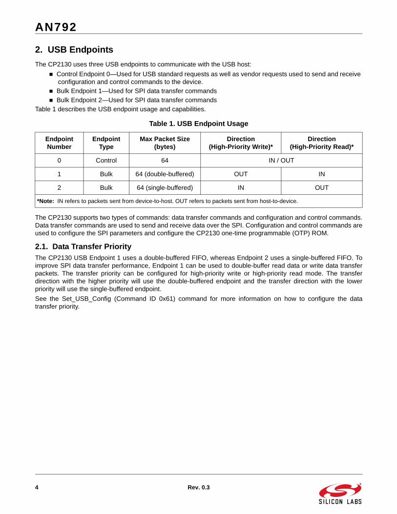
2. USB Endpoints
The CP2130 uses three USB endpoints to communicate with the USB host:
Control Endpoint 0—Used for USB standard requests as well as vendor requests used to send and receive configuration and control commands to the device.
Bulk Endpoint 1—Used for SPI data transfer commands
Bulk Endpoint 2—Used for SPI data transfer commands
Table 1 describes the USB endpoint usage and capabilities.
The CP2130 supports two types of commands: data transfer commands and configuration and control commands.Data transfer commands are used to send and receive data over the SPI. Configuration and control commands areused to configure the SPI parameters and configure the CP2130 one-time programmable (OTP) ROM.
2.1. Data Transfer PriorityThe CP2130 USB Endpoint 1 uses a double-buffered FIFO, whereas Endpoint 2 uses a single-buffered FIFO. Toimprove SPI data transfer performance, Endpoint 1 can be used to double-buffer read data or write data transferpackets. The transfer priority can be configured for high-priority write or high-priority read mode. The transferdirection with the higher priority will use the double-buffered endpoint and the transfer direction with the lowerpriority will use the single-buffered endpoint.
See the Set_USB_Config (Command ID 0x61) command for more information on how to configure the datatransfer priority.
Table 1. USB Endpoint Usage
Endpoint Number
Endpoint Type
Max Packet Size (bytes)
Direction(High-Priority Write)*
Direction(High-Priority Read)*
0 Control 64 IN / OUT
1 Bulk 64 (double-buffered) OUT IN
2 Bulk 64 (single-buffered) IN OUT
*Note: IN refers to packets sent from device-to-host. OUT refers to packets sent from host-to-device.
AN792
Rev. 0.3 5
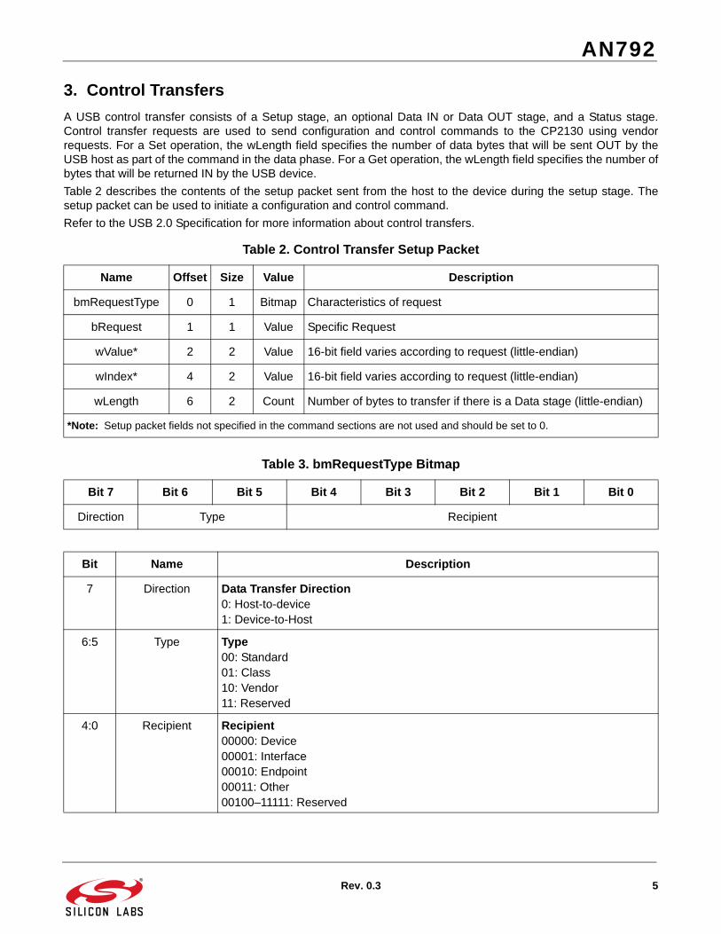
3. Control Transfers
A USB control transfer consists of a Setup stage, an optional Data IN or Data OUT stage, and a Status stage.Control transfer requests are used to send configuration and control commands to the CP2130 using vendorrequests. For a Set operation, the wLength field specifies the number of data bytes that will be sent OUT by theUSB host as part of the command in the data phase. For a Get operation, the wLength field specifies the number ofbytes that will be returned IN by the USB device.
Table 2 describes the contents of the setup packet sent from the host to the device during the setup stage. Thesetup packet can be used to initiate a configuration and control command.
Refer to the USB 2.0 Specification for more information about control transfers.
Table 2. Control Transfer Setup Packet
Name Offset Size Value Description
bmRequestType 0 1 Bitmap Characteristics of request
bRequest 1 1 Value Specific Request
wValue* 2 2 Value 16-bit field varies according to request (little-endian)
wIndex* 4 2 Value 16-bit field varies according to request (little-endian)
wLength 6 2 Count Number of bytes to transfer if there is a Data stage (little-endian)
*Note: Setup packet fields not specified in the command sections are not used and should be set to 0.
Table 3. bmRequestType Bitmap
Bit 7 Bit 6 Bit 5 Bit 4 Bit 3 Bit 2 Bit 1 Bit 0
Direction Type Recipient
Bit Name Description
7 Direction Data Transfer Direction0: Host-to-device1: Device-to-Host
6:5 Type Type00: Standard01: Class10: Vendor11: Reserved
4:0 Recipient Recipient00000: Device00001: Interface00010: Endpoint00011: Other00100–11111: Reserved
AN792
6 Rev. 0.3
4. Multi-Byte Field Endianness
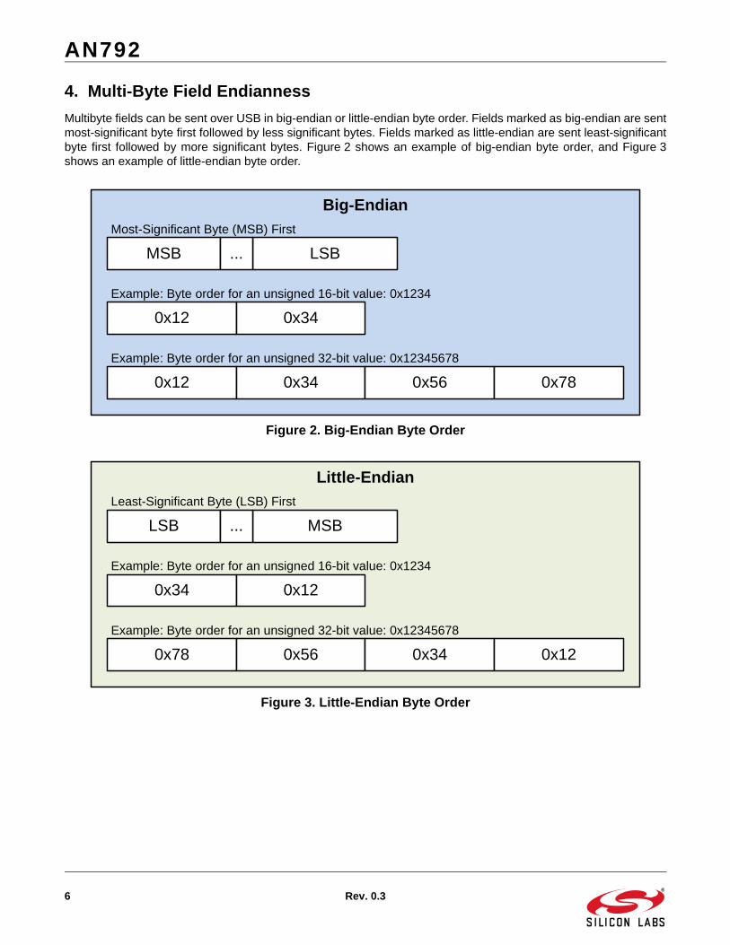
Multibyte fields can be sent over USB in big-endian or little-endian byte order. Fields marked as big-endian are sentmost-significant byte first followed by less significant bytes. Fields marked as little-endian are sent least-significantbyte first followed by more significant bytes. Figure 2 shows an example of big-endian byte order, and Figure 3shows an example of little-endian byte order.
Figure 2. Big-Endian Byte Order
Figure 3. Little-Endian Byte Order
MSB LSB...
Most-Significant Byte (MSB) First
0x12 0x34
Example: Byte order for an unsigned 16-bit value: 0x1234
Big-Endian
0x12
Example: Byte order for an unsigned 32-bit value: 0x12345678
0x34 0x56 0x78
LSB MSB...
Least-Significant Byte (LSB) First
0x34 0x12
Example: Byte order for an unsigned 16-bit value: 0x1234
Little-Endian
0x78
Example: Byte order for an unsigned 32-bit value: 0x12345678
0x56 0x34 0x12

AN792
Rev. 0.3 7
5. Data Transfer Commands (Bulk Transfers)
Data transfer commands from USB to SPI are implemented using USB bulk-mode transfers on USB Endpoints 1and 2. The direction of Endpoint 1 and Endpoint 2 are dependent on the Transfer Priority setting.
Any previous data transfer command must complete before another data transfer command is issued. The hostmay issue control commands (on Endpoint 0) while data transfer commands are in progress.
A summary of these commands is given in Table 4 with detailed descriptions in following sections.
Table 4. Data Transfer Commands
Command Name
Command ID Comment Page
Read 0x00 Reads data from the SPI MISO line to USB 8
Write 0x01 Write data from USB to the SPI MOSI line. 9
WriteRead 0x02 Simultaneous Write/Read from USB to MOSI/MISO 10
ReadWithRTR 0x04 Read data when RTR (ReadyToRead) pin is asserted 11
AN792
8 Rev. 0.3
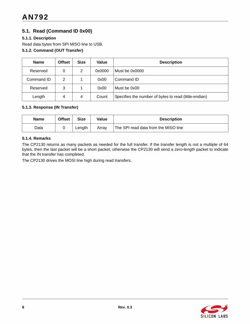
5.1. Read (Command ID 0x00)5.1.1. Description
Read data bytes from SPI MISO line to USB.
5.1.2. Command (OUT Transfer)
5.1.3. Response (IN Transfer)
5.1.4. Remarks
The CP2130 returns as many packets as needed for the full transfer. If the transfer length is not a multiple of 64bytes, then the last packet will be a short packet; otherwise the CP2130 will send a zero-length packet to indicatethat the IN transfer has completed.
The CP2130 drives the MOSI line high during read transfers.
Name Offset Size Value Description
Reserved 0 2 0x0000 Must be 0x0000
Command ID 2 1 0x00 Command ID
Reserved 3 1 0x00 Must be 0x00
Length 4 4 Count Specifies the number of bytes to read (little-endian)
Name Offset Size Value Description
Data 0 Length Array The SPI read data from the MISO line
AN792
Rev. 0.3 9
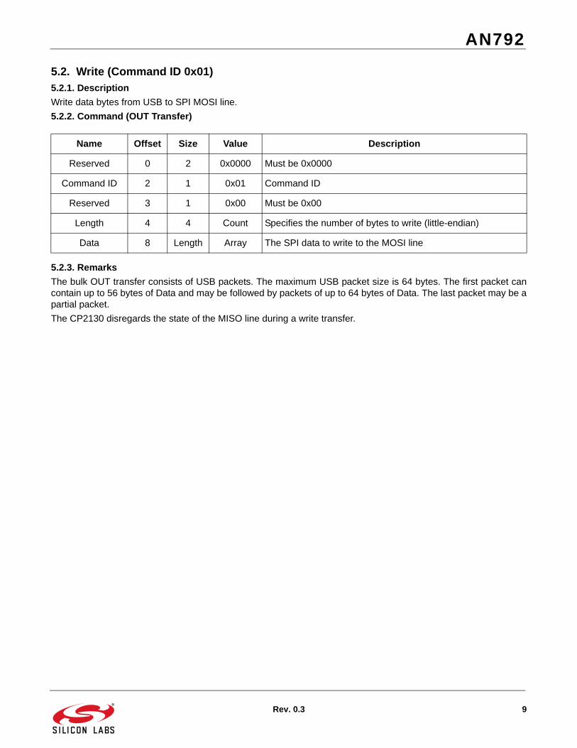
5.2. Write (Command ID 0x01)5.2.1. Description
Write data bytes from USB to SPI MOSI line.
5.2.2. Command (OUT Transfer)
5.2.3. Remarks
The bulk OUT transfer consists of USB packets. The maximum USB packet size is 64 bytes. The first packet cancontain up to 56 bytes of Data and may be followed by packets of up to 64 bytes of Data. The last packet may be apartial packet.
The CP2130 disregards the state of the MISO line during a write transfer.
Name Offset Size Value Description
Reserved 0 2 0x0000 Must be 0x0000
Command ID 2 1 0x01 Command ID
Reserved 3 1 0x00 Must be 0x00
Length 4 4 Count Specifies the number of bytes to write (little-endian)
Data 8 Length Array The SPI data to write to the MOSI line
AN792
10 Rev. 0.3
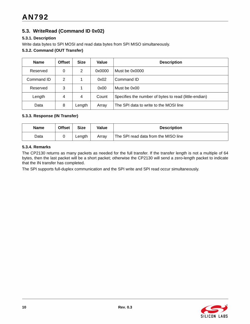
5.3. WriteRead (Command ID 0x02)5.3.1. Description
Write data bytes to SPI MOSI and read data bytes from SPI MISO simultaneously.
5.3.2. Command (OUT Transfer)
5.3.3. Response (IN Transfer)
5.3.4. Remarks
The CP2130 returns as many packets as needed for the full transfer. If the transfer length is not a multiple of 64bytes, then the last packet will be a short packet; otherwise the CP2130 will send a zero-length packet to indicatethat the IN transfer has completed.
The SPI supports full-duplex communication and the SPI write and SPI read occur simultaneously.
Name Offset Size Value Description
Reserved 0 2 0x0000 Must be 0x0000
Command ID 2 1 0x02 Command ID
Reserved 3 1 0x00 Must be 0x00
Length 4 4 Count Specifies the number of bytes to read (little-endian)
Data 8 Length Array The SPI data to write to the MOSI line
Name Offset Size Value Description
Data 0 Length Array The SPI read data from the MISO line

AN792
Rev. 0.3 11
5.4. ReadWithRTR (Command ID 0x04)5.4.1. Description
Read data bytes from SPI MISO to USB as long as the RTR pin (GPIO.3 / CS3 / RTR) is asserted. Pause the readif RTR (ready-to-read) is not asserted.
5.4.2. Command (OUT Transfer)
5.4.3. Response (IN Transfer)
5.4.4. Remarks
The CP2130 returns as many packets as needed for the full transfer. If the transfer length is not a multiple of 64bytes, then the last packet will be a short packet; otherwise the CP2130 will send a zero-length packet to indicatethat the IN transfer has completed.
The CP2130 drives the MOSI line high during read transfers.
The SPI byte transfers will be paused if the RTR pin is not asserted. SPI byte transfers will resume when RTR isasserted.
Name Offset Size Value Description
Reserved 0 2 0x0000 Must be 0x0000
Command ID 2 1 0x04 Command ID
Reserved 3 1 0x00 Must be 0x00
Length 4 4 Count Specifies the number of bytes to read (little-endian)
Name Offset Size Value Description
Data 0 Length Array The SPI read data from the MISO line
AN792
12 Rev. 0.3
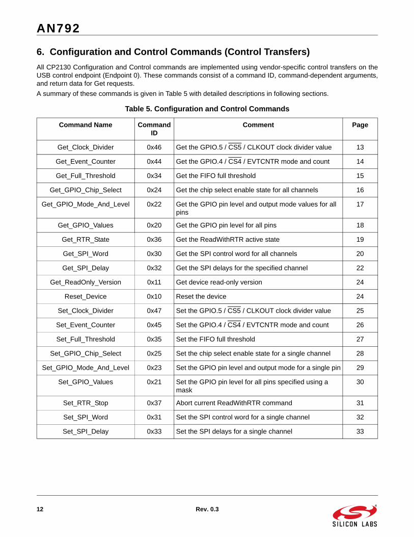
6. Configuration and Control Commands (Control Transfers)
All CP2130 Configuration and Control commands are implemented using vendor-specific control transfers on theUSB control endpoint (Endpoint 0). These commands consist of a command ID, command-dependent arguments,and return data for Get requests.
A summary of these commands is given in Table 5 with detailed descriptions in following sections.
Table 5. Configuration and Control Commands
Command Name Command ID
Comment Page
Get_Clock_Divider 0x46 Get the GPIO.5 / CS5 / CLKOUT clock divider value 13
Get_Event_Counter 0x44 Get the GPIO.4 / CS4 / EVTCNTR mode and count 14
Get_Full_Threshold 0x34 Get the FIFO full threshold 15
Get_GPIO_Chip_Select 0x24 Get the chip select enable state for all channels 16
Get_GPIO_Mode_And_Level 0x22 Get the GPIO pin level and output mode values for all pins
17
Get_GPIO_Values 0x20 Get the GPIO pin level for all pins 18
Get_RTR_State 0x36 Get the ReadWithRTR active state 19
Get_SPI_Word 0x30 Get the SPI control word for all channels 20
Get_SPI_Delay 0x32 Get the SPI delays for the specified channel 22
Get_ReadOnly_Version 0x11 Get device read-only version 24
Reset_Device 0x10 Reset the device 24
Set_Clock_Divider 0x47 Set the GPIO.5 / CS5 / CLKOUT clock divider value 25
Set_Event_Counter 0x45 Set the GPIO.4 / CS4 / EVTCNTR mode and count 26
Set_Full_Threshold 0x35 Set the FIFO full threshold 27
Set_GPIO_Chip_Select 0x25 Set the chip select enable state for a single channel 28
Set_GPIO_Mode_And_Level 0x23 Set the GPIO pin level and output mode for a single pin 29
Set_GPIO_Values 0x21 Set the GPIO pin level for all pins specified using a mask
30
Set_RTR_Stop 0x37 Abort current ReadWithRTR command 31
Set_SPI_Word 0x31 Set the SPI control word for a single channel 32
Set_SPI_Delay 0x33 Set the SPI delays for a single channel 33

AN792
Rev. 0.3 13
6.1. Get_Clock_Divider (Command ID 0x46)6.1.1. Description
Get the GPIO.5 / CS5 / CLKOUT clock divider value.
6.1.2. Setup Stage (OUT Transfer)
6.1.3. Data Stage (IN Transfer)
6.1.4. Remarks and Related Commands
GPIO.5 / CS5 / CLKOUT must be configured in CLKOUT mode in order to generate the clock output.
The output frequency is configurable through the use of the clock divider. When the divider is set to 0, the outputfrequency is 93.75 kHz. For divider values between 1 and 255, the output frequency is determined by the formula:
See also Set_Clock_Divider (Command ID 0x47).
Name Value Description
bmRequestType 0xC0 Device-to-Host vendor request
bRequest 0x46 Command ID
wLength 0x0001 Data stage length in bytes
Name Offset Size Value Description
Divider 0 1 Value The GPIO.5 / CS5 / CLKOUT clock divider value. A value of 0 indicates a divider value of 256.
GPIO.5 Clock Frequency24 MHzDivider---------------------=
AN792
14 Rev. 0.3
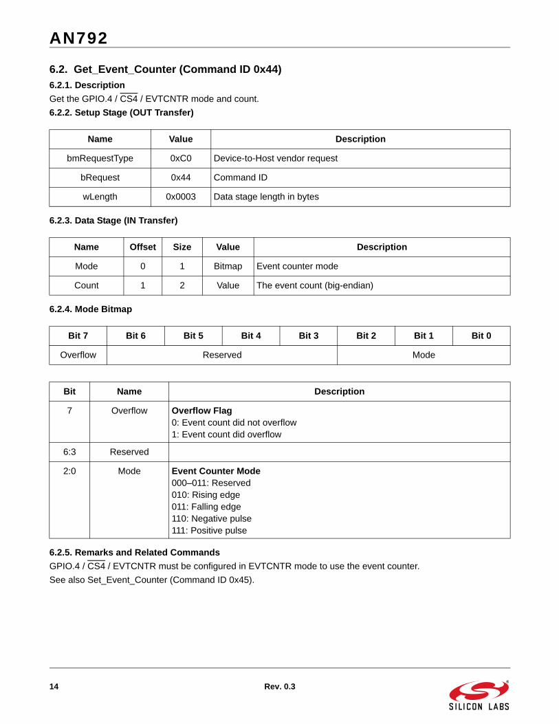
6.2. Get_Event_Counter (Command ID 0x44)6.2.1. Description
Get the GPIO.4 / CS4 / EVTCNTR mode and count.
6.2.2. Setup Stage (OUT Transfer)
6.2.3. Data Stage (IN Transfer)
6.2.4. Mode Bitmap
6.2.5. Remarks and Related Commands
GPIO.4 / CS4 / EVTCNTR must be configured in EVTCNTR mode to use the event counter.
See also Set_Event_Counter (Command ID 0x45).
Name Value Description
bmRequestType 0xC0 Device-to-Host vendor request
bRequest 0x44 Command ID
wLength 0x0003 Data stage length in bytes
Name Offset Size Value Description
Mode 0 1 Bitmap Event counter mode
Count 1 2 Value The event count (big-endian)
Bit 7 Bit 6 Bit 5 Bit 4 Bit 3 Bit 2 Bit 1 Bit 0
Overflow Reserved Mode
Bit Name Description
7 Overflow Overflow Flag0: Event count did not overflow1: Event count did overflow
6:3 Reserved
2:0 Mode Event Counter Mode000–011: Reserved010: Rising edge011: Falling edge110: Negative pulse111: Positive pulse

AN792
Rev. 0.3 15
6.3. Get_Full_Threshold (Command ID 0x34)6.3.1. Description
Get the FIFO full threshold.
6.3.2. Setup Stage (OUT Transfer)
6.3.3. Data Stage (IN Transfer)
6.3.4. Remarks and Related Commands
See also Set_Full_Threshold (Command ID 0x35).
Name Value Description
bmRequestType 0xC0 Device-to-Host vendor request
bRequest 0x34 Command ID
wLength 0x0001 Data stage length in bytes
Name Offset Size Value Description
Threshold 0 1 Value The FIFO full threshold. Default is 128 bytes.
AN792
16 Rev. 0.3
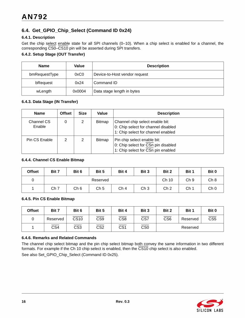
6.4. Get_GPIO_Chip_Select (Command ID 0x24)6.4.1. Description
Get the chip select enable state for all SPI channels (0–10). When a chip select is enabled for a channel, thecorresponding CS0–CS10 pin will be asserted during SPI transfers.
6.4.2. Setup Stage (OUT Transfer)
6.4.3. Data Stage (IN Transfer)
6.4.4. Channel CS Enable Bitmap
6.4.5. Pin CS Enable Bitmap
6.4.6. Remarks and Related Commands
The channel chip select bitmap and the pin chip select bitmap both convey the same information in two differentformats. For example if the Ch 10 chip select is enabled, then the CS10 chip select is also enabled.
See also Set_GPIO_Chip_Select (Command ID 0x25).
Name Value Description
bmRequestType 0xC0 Device-to-Host vendor request
bRequest 0x24 Command ID
wLength 0x0004 Data stage length in bytes
Name Offset Size Value Description
Channel CS Enable
0 2 Bitmap Channel chip select enable bit:0: Chip select for channel disabled1: Chip select for channel enabled
Pin CS Enable 2 2 Bitmap Pin chip select enable bit:0: Chip select for CSn pin disabled1: Chip select for CSn pin enabled
Offset Bit 7 Bit 6 Bit 5 Bit 4 Bit 3 Bit 2 Bit 1 Bit 0
0 Reserved Ch 10 Ch 9 Ch 8
1 Ch 7 Ch 6 Ch 5 Ch 4 Ch 3 Ch 2 Ch 1 Ch 0
Offset Bit 7 Bit 6 Bit 5 Bit 4 Bit 3 Bit 2 Bit 1 Bit 0
0 Reserved CS10 CS9 CS8 CS7 CS6 Reserved CS5
1 CS4 CS3 CS2 CS1 CS0 Reserved
AN792
Rev. 0.3 17
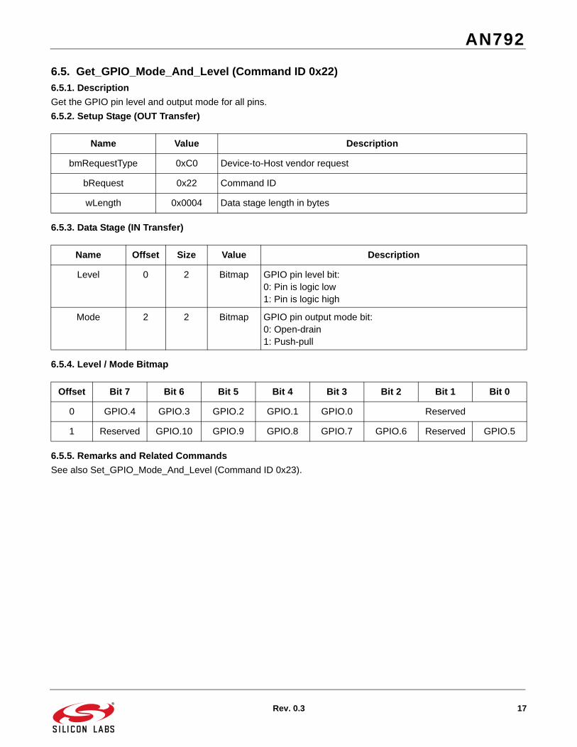
6.5. Get_GPIO_Mode_And_Level (Command ID 0x22)6.5.1. Description
Get the GPIO pin level and output mode for all pins.
6.5.2. Setup Stage (OUT Transfer)
6.5.3. Data Stage (IN Transfer)
6.5.4. Level / Mode Bitmap
6.5.5. Remarks and Related Commands
See also Set_GPIO_Mode_And_Level (Command ID 0x23).
Name Value Description
bmRequestType 0xC0 Device-to-Host vendor request
bRequest 0x22 Command ID
wLength 0x0004 Data stage length in bytes
Name Offset Size Value Description
Level 0 2 Bitmap GPIO pin level bit:0: Pin is logic low1: Pin is logic high
Mode 2 2 Bitmap GPIO pin output mode bit:0: Open-drain1: Push-pull
Offset Bit 7 Bit 6 Bit 5 Bit 4 Bit 3 Bit 2 Bit 1 Bit 0
0 GPIO.4 GPIO.3 GPIO.2 GPIO.1 GPIO.0 Reserved
1 Reserved GPIO.10 GPIO.9 GPIO.8 GPIO.7 GPIO.6 Reserved GPIO.5
AN792
18 Rev. 0.3
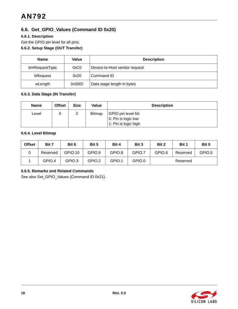
6.6. Get_GPIO_Values (Command ID 0x20)6.6.1. Description
Get the GPIO pin level for all pins.
6.6.2. Setup Stage (OUT Transfer)
6.6.3. Data Stage (IN Transfer)
6.6.4. Level Bitmap
6.6.5. Remarks and Related Commands
See also Set_GPIO_Values (Command ID 0x21).
Name Value Description
bmRequestType 0xC0 Device-to-Host vendor request
bRequest 0x20 Command ID
wLength 0x0002 Data stage length in bytes
Name Offset Size Value Description
Level 0 2 Bitmap GPIO pin level bit:0: Pin is logic low1: Pin is logic high
Offset Bit 7 Bit 6 Bit 5 Bit 4 Bit 3 Bit 2 Bit 1 Bit 0
0 Reserved GPIO.10 GPIO.9 GPIO.8 GPIO.7 GPIO.6 Reserved GPIO.5
1 GPIO.4 GPIO.3 GPIO.2 GPIO.1 GPIO.0 Reserved
AN792
Rev. 0.3 19
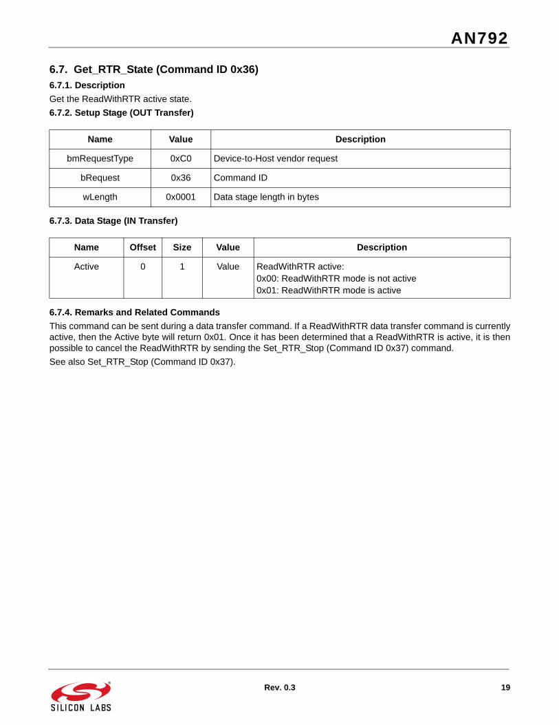
6.7. Get_RTR_State (Command ID 0x36)6.7.1. Description
Get the ReadWithRTR active state.
6.7.2. Setup Stage (OUT Transfer)
6.7.3. Data Stage (IN Transfer)
6.7.4. Remarks and Related Commands
This command can be sent during a data transfer command. If a ReadWithRTR data transfer command is currentlyactive, then the Active byte will return 0x01. Once it has been determined that a ReadWithRTR is active, it is thenpossible to cancel the ReadWithRTR by sending the Set_RTR_Stop (Command ID 0x37) command.
See also Set_RTR_Stop (Command ID 0x37).
Name Value Description
bmRequestType 0xC0 Device-to-Host vendor request
bRequest 0x36 Command ID
wLength 0x0001 Data stage length in bytes
Name Offset Size Value Description
Active 0 1 Value ReadWithRTR active:0x00: ReadWithRTR mode is not active0x01: ReadWithRTR mode is active
AN792
20 Rev. 0.3
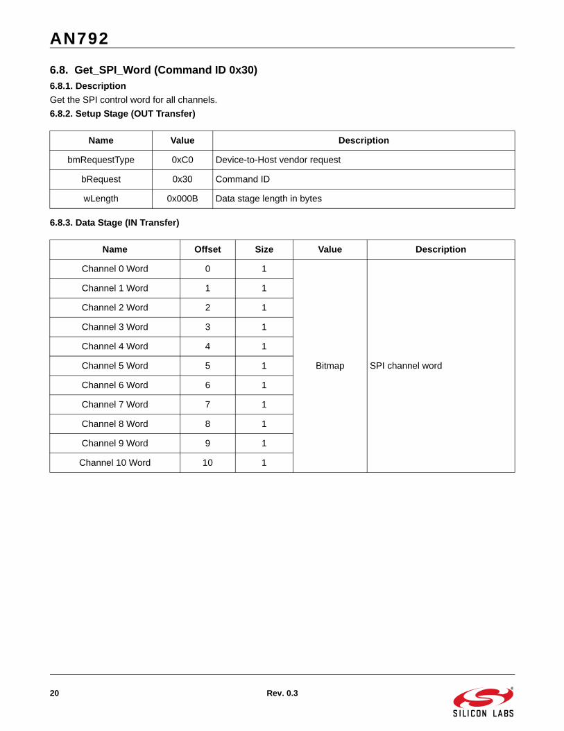
6.8. Get_SPI_Word (Command ID 0x30)6.8.1. Description
Get the SPI control word for all channels.
6.8.2. Setup Stage (OUT Transfer)
6.8.3. Data Stage (IN Transfer)
Name Value Description
bmRequestType 0xC0 Device-to-Host vendor request
bRequest 0x30 Command ID
wLength 0x000B Data stage length in bytes
Name Offset Size Value Description
Channel 0 Word 0 1
Bitmap SPI channel word
Channel 1 Word 1 1
Channel 2 Word 2 1
Channel 3 Word 3 1
Channel 4 Word 4 1
Channel 5 Word 5 1
Channel 6 Word 6 1
Channel 7 Word 7 1
Channel 8 Word 8 1
Channel 9 Word 9 1
Channel 10 Word 10 1
AN792
Rev. 0.3 21
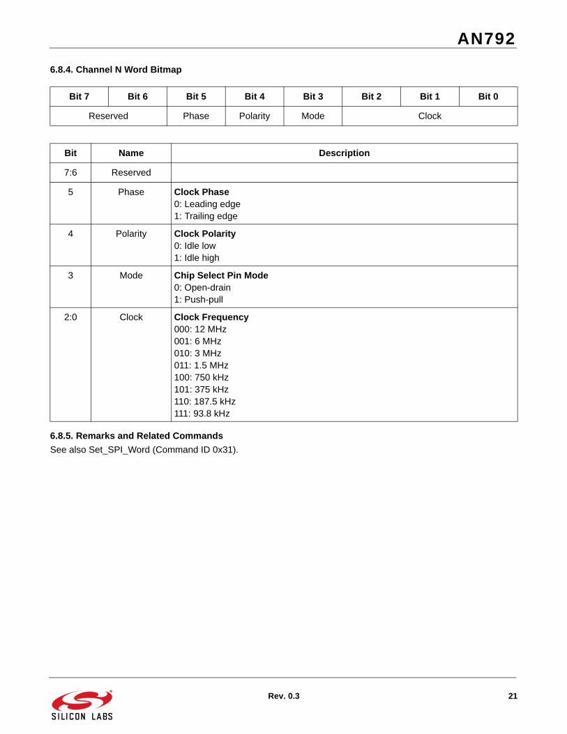
6.8.4. Channel N Word Bitmap
6.8.5. Remarks and Related Commands
See also Set_SPI_Word (Command ID 0x31).
Bit 7 Bit 6 Bit 5 Bit 4 Bit 3 Bit 2 Bit 1 Bit 0
Reserved Phase Polarity Mode Clock
Bit Name Description
7:6 Reserved
5 Phase Clock Phase0: Leading edge1: Trailing edge
4 Polarity Clock Polarity0: Idle low1: Idle high
3 Mode Chip Select Pin Mode0: Open-drain1: Push-pull
2:0 Clock Clock Frequency000: 12 MHz001: 6 MHz010: 3 MHz011: 1.5 MHz100: 750 kHz101: 375 kHz110: 187.5 kHz111: 93.8 kHz
AN792
22 Rev. 0.3
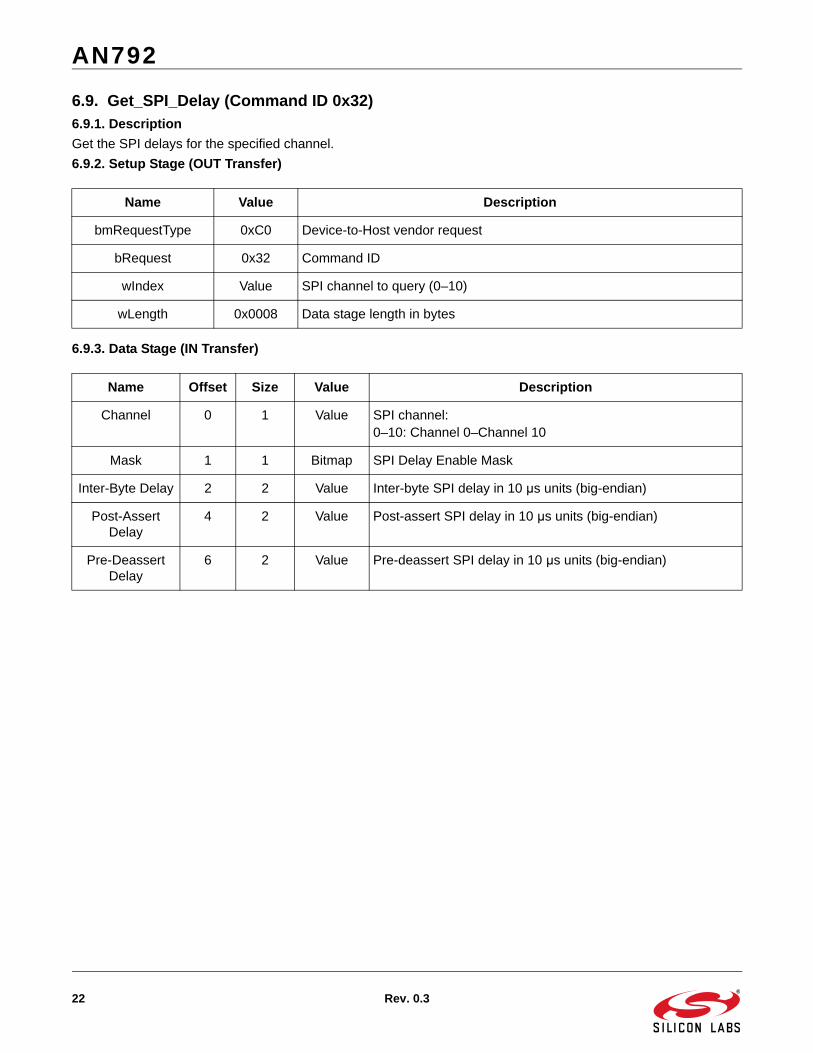
6.9. Get_SPI_Delay (Command ID 0x32)6.9.1. Description
Get the SPI delays for the specified channel.
6.9.2. Setup Stage (OUT Transfer)
6.9.3. Data Stage (IN Transfer)
Name Value Description
bmRequestType 0xC0 Device-to-Host vendor request
bRequest 0x32 Command ID
wIndex Value SPI channel to query (0–10)
wLength 0x0008 Data stage length in bytes
Name Offset Size Value Description
Channel 0 1 Value SPI channel:0–10: Channel 0–Channel 10
Mask 1 1 Bitmap SPI Delay Enable Mask
Inter-Byte Delay 2 2 Value Inter-byte SPI delay in 10 μs units (big-endian)
Post-Assert Delay
4 2 Value Post-assert SPI delay in 10 μs units (big-endian)
Pre-Deassert Delay
6 2 Value Pre-deassert SPI delay in 10 μs units (big-endian)
AN792
Rev. 0.3 23
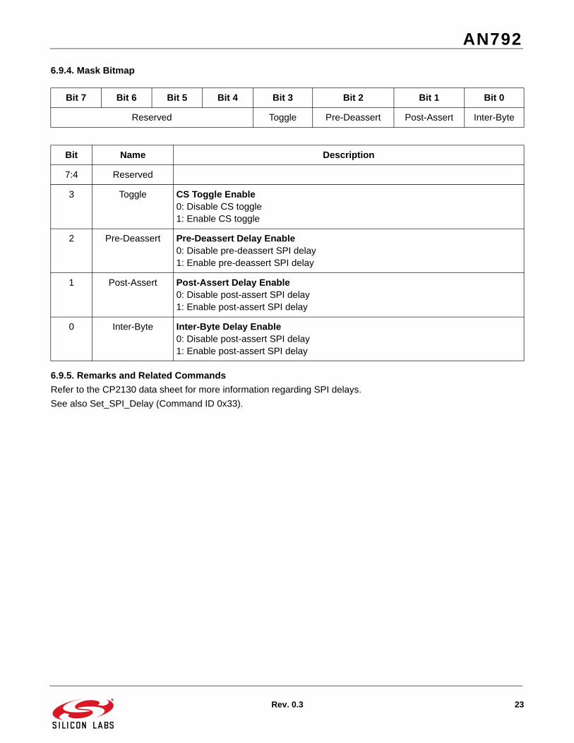
6.9.4. Mask Bitmap
6.9.5. Remarks and Related Commands
Refer to the CP2130 data sheet for more information regarding SPI delays.
See also Set_SPI_Delay (Command ID 0x33).
Bit 7 Bit 6 Bit 5 Bit 4 Bit 3 Bit 2 Bit 1 Bit 0
Reserved Toggle Pre-Deassert Post-Assert Inter-Byte
Bit Name Description
7:4 Reserved
3 Toggle CS Toggle Enable0: Disable CS toggle1: Enable CS toggle
2 Pre-Deassert Pre-Deassert Delay Enable0: Disable pre-deassert SPI delay1: Enable pre-deassert SPI delay
1 Post-Assert Post-Assert Delay Enable0: Disable post-assert SPI delay1: Enable post-assert SPI delay
0 Inter-Byte Inter-Byte Delay Enable0: Disable post-assert SPI delay1: Enable post-assert SPI delay
AN792
24 Rev. 0.3
6.10. Get_ReadOnly_Version (Command ID 0x11)6.10.1. Description
Get the device read-only version.
6.10.2. Setup Stage (OUT Transfer)
6.10.3. Data Stage (IN Transfer)
6.10.4. Remarks
The device read-only version number reports the CP2130 hardware version number. This version cannot bemodified by the user. This document is compatible with version 1.0.
6.11. Reset_Device (Command ID 0x10)6.11.1. Description
Reset the device.
6.11.2. Setup Stage (OUT Transfer)
6.11.3. Remarks
This command is a host-to-device request with no data stage. Approximately one millisecond after receiving thisrequest, the device will reset and re-enumerate on the USB host.
Name Value Description
bmRequestType 0xC0 Device-to-Host vendor request
bRequest 0x11 Command ID
wLength 0x0002 Data stage length in bytes
Name Offset Size Value Description
Major Version 0 1 0x01 Major read-only version number
Minor Version 1 1 0x00 Minor read-only version number
Name Value Description
bmRequestType 0x40 Host-to-Device vendor request
bRequest 0x10 Command ID
wLength 0x0000 Data stage length in bytes
AN792
Rev. 0.3 25
6.12. Set_Clock_Divider (Command ID 0x47)6.12.1. Description
Set the GPIO.5 / CS5 / CLKOUT clock divider value.
6.12.2. Setup Stage (OUT Transfer)
6.12.3. Data Stage (OUT Transfer)
6.12.4. Remarks and Related Commands
GPIO.5 / CS5 / CLKOUT must be configured in CLKOUT mode in order to generate the clock output.
The output frequency is configurable through the use of the clock divider. When the divider is set to 0, the outputfrequency is 93.75 kHz. For divider values between 1 and 255, the output frequency is determined by the formula:
See also Get_Clock_Divider (Command ID 0x46).
Name Value Description
bmRequestType 0x40 Host-to-Device vendor request
bRequest 0x47 Command ID
wLength 0x0001 Data stage length in bytes
Name Offset Size Value Description
Divider 0 1 Value The GPIO.5 / CS5 / CLKOUT clock divider value. A value of 0 indicates a divider value of 256.
GPIO.5 Clock Frequency24 MHzDivider---------------------=
AN792
26 Rev. 0.3
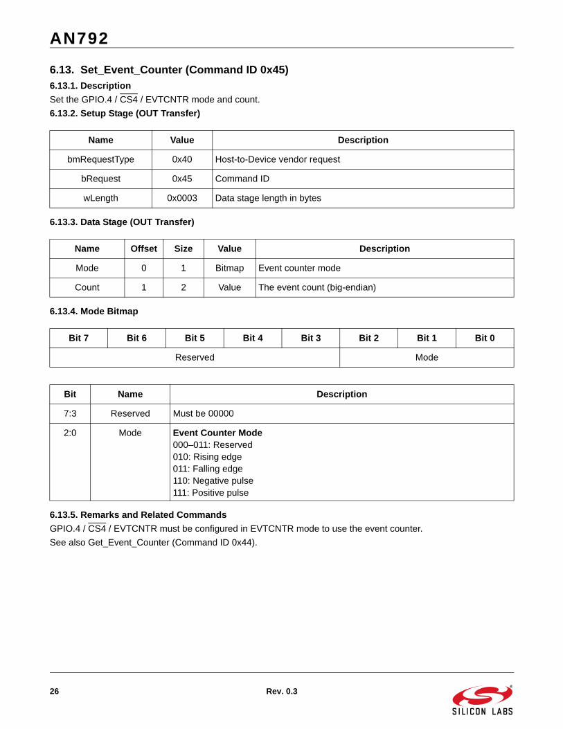
6.13. Set_Event_Counter (Command ID 0x45)6.13.1. Description
Set the GPIO.4 / CS4 / EVTCNTR mode and count.
6.13.2. Setup Stage (OUT Transfer)
6.13.3. Data Stage (OUT Transfer)
6.13.4. Mode Bitmap
6.13.5. Remarks and Related Commands
GPIO.4 / CS4 / EVTCNTR must be configured in EVTCNTR mode to use the event counter.
See also Get_Event_Counter (Command ID 0x44).
Name Value Description
bmRequestType 0x40 Host-to-Device vendor request
bRequest 0x45 Command ID
wLength 0x0003 Data stage length in bytes
Name Offset Size Value Description
Mode 0 1 Bitmap Event counter mode
Count 1 2 Value The event count (big-endian)
Bit 7 Bit 6 Bit 5 Bit 4 Bit 3 Bit 2 Bit 1 Bit 0
Reserved Mode
Bit Name Description
7:3 Reserved Must be 00000
2:0 Mode Event Counter Mode000–011: Reserved010: Rising edge011: Falling edge110: Negative pulse111: Positive pulse
AN792
Rev. 0.3 27
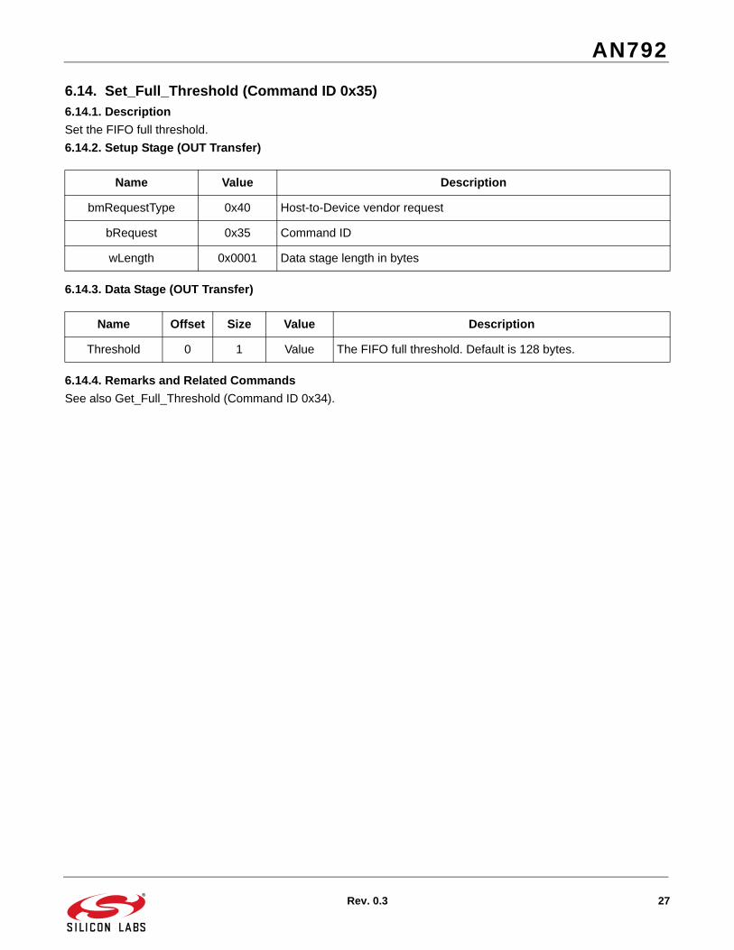
6.14. Set_Full_Threshold (Command ID 0x35)6.14.1. Description
Set the FIFO full threshold.
6.14.2. Setup Stage (OUT Transfer)
6.14.3. Data Stage (OUT Transfer)
6.14.4. Remarks and Related Commands
See also Get_Full_Threshold (Command ID 0x34).
Name Value Description
bmRequestType 0x40 Host-to-Device vendor request
bRequest 0x35 Command ID
wLength 0x0001 Data stage length in bytes
Name Offset Size Value Description
Threshold 0 1 Value The FIFO full threshold. Default is 128 bytes.

AN792
28 Rev. 0.3
6.15. Set_GPIO_Chip_Select (Command ID 0x25)6.15.1. Description
Set the chip select enable state for the specified channel. When a chip select is enabled for a channel, thecorresponding CS0–CS10 pin will be asserted during SPI transfers and the SPI word for the specified channel willbe used to configure the SPI.
6.15.2. Setup Stage (OUT Transfer)
6.15.3. Data Stage (OUT Transfer)
6.15.4. Remarks and Related Commands
Multiple chip selects can be enabled by sending this command with Control set to 0x01. Sending this commandwith Control set to 0x01 or 0x02 also sets the active SPI channel to the channel specified. This means that the lastchip select enabled determines which SPI word setting to use based on channel number.
The Set_SPI_Word (Command ID 0x31) command can be used to specify the SPI configuration for each channel.The Set_GPIO_Chip_Select (Command ID 0x25) command can then be used to select the active channel.
See also Get_GPIO_Chip_Select (Command ID 0x24).
Name Value Description
bmRequestType 0x40 Host-to-Device vendor request
bRequest 0x25 Command ID
wLength 0x0002 Data stage length in bytes
Name Offset Size Value Description
Channel 0 1 Value Chip select channel (0–10)
Control 1 1 Value Chip select channel control:0x00: Specified chip select is disabled0x01: Specified chip select is enabled during SPI transfers0x02: Specified chip select is enabled during SPI transfers; all other chip selects are disabled
AN792
Rev. 0.3 29
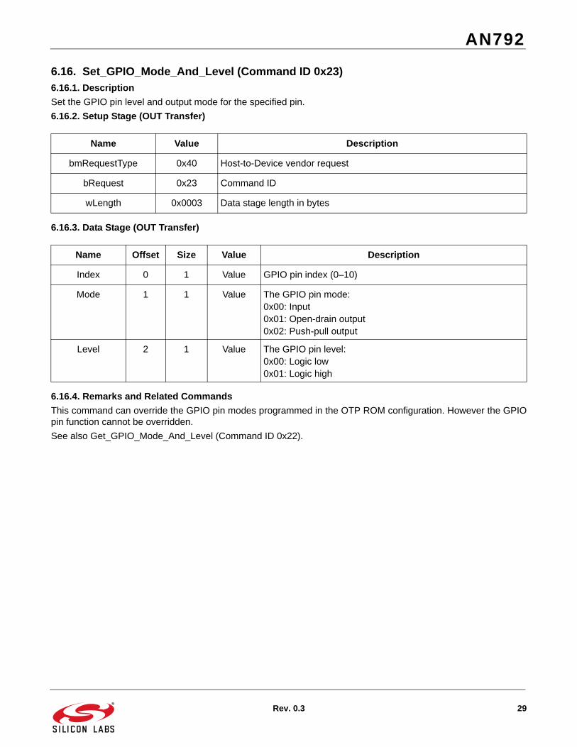
6.16. Set_GPIO_Mode_And_Level (Command ID 0x23)6.16.1. Description
Set the GPIO pin level and output mode for the specified pin.
6.16.2. Setup Stage (OUT Transfer)
6.16.3. Data Stage (OUT Transfer)
6.16.4. Remarks and Related Commands
This command can override the GPIO pin modes programmed in the OTP ROM configuration. However the GPIOpin function cannot be overridden.
See also Get_GPIO_Mode_And_Level (Command ID 0x22).
Name Value Description
bmRequestType 0x40 Host-to-Device vendor request
bRequest 0x23 Command ID
wLength 0x0003 Data stage length in bytes
Name Offset Size Value Description
Index 0 1 Value GPIO pin index (0–10)
Mode 1 1 Value The GPIO pin mode:0x00: Input0x01: Open-drain output0x02: Push-pull output
Level 2 1 Value The GPIO pin level:0x00: Logic low0x01: Logic high
AN792
30 Rev. 0.3
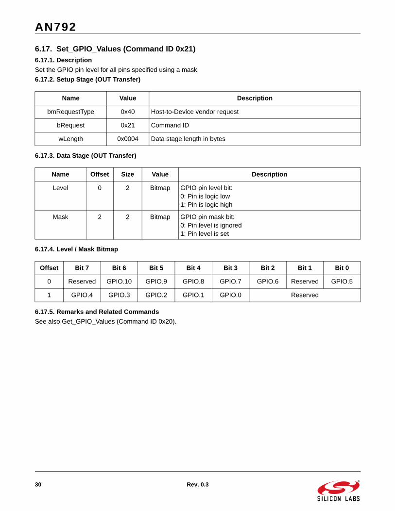
6.17. Set_GPIO_Values (Command ID 0x21)6.17.1. Description
Set the GPIO pin level for all pins specified using a mask
6.17.2. Setup Stage (OUT Transfer)
6.17.3. Data Stage (OUT Transfer)
6.17.4. Level / Mask Bitmap
6.17.5. Remarks and Related Commands
See also Get_GPIO_Values (Command ID 0x20).
Name Value Description
bmRequestType 0x40 Host-to-Device vendor request
bRequest 0x21 Command ID
wLength 0x0004 Data stage length in bytes
Name Offset Size Value Description
Level 0 2 Bitmap GPIO pin level bit:0: Pin is logic low1: Pin is logic high
Mask 2 2 Bitmap GPIO pin mask bit:0: Pin level is ignored1: Pin level is set
Offset Bit 7 Bit 6 Bit 5 Bit 4 Bit 3 Bit 2 Bit 1 Bit 0
0 Reserved GPIO.10 GPIO.9 GPIO.8 GPIO.7 GPIO.6 Reserved GPIO.5
1 GPIO.4 GPIO.3 GPIO.2 GPIO.1 GPIO.0 Reserved

AN792
Rev. 0.3 31
6.18. Set_RTR_Stop (Command ID 0x37)6.18.1. Description
Abort the current ReadWithRTR command.
6.18.2. Setup Stage (OUT Transfer)
6.18.3. Data Stage (OUT Transfer)
6.18.4. Remarks and Related Commands
See also Get_RTR_State (Command ID 0x36).
Name Value Description
bmRequestType 0x40 Host-to-Device vendor request
bRequest 0x37 Command ID
wLength 0x0001 Data stage length in bytes
Name Offset Size Value Description
Abort 0 1 Value Abort ReadWithRTR:0x00: No effect0x01: Abort current ReadWithRTR command

AN792
32 Rev. 0.3
6.19. Set_SPI_Word (Command ID 0x31)6.19.1. Description
Set the SPI control word for a single channel.
6.19.2. Setup Stage (OUT Transfer)
6.19.3. Data Stage (OUT Transfer)
6.19.4. Channel Word Bitmap
6.19.5. Remarks and Related Commands
See also Get_SPI_Word (Command ID 0x30).
Name Value Description
bmRequestType 0x40 Host-to-Device vendor request
bRequest 0x31 Command ID
wLength 0x0002 Data stage length in bytes
Name Offset Size Value Description
Channel 0 1 Value SPI channel:0–10: Channel 0–Channel 10
Channel Word 1 1 Bitmap SPI channel word
Bit 7 Bit 6 Bit 5 Bit 4 Bit 3 Bit 2 Bit 1 Bit 0
Reserved Phase Polarity Mode Clock
Bit Name Description
7:6 Reserved
5 Phase Clock Phase0: Leading edge1: Trailing edge
4 Polarity Clock Polarity0: Idle low1: Idle high
3 Mode Chip Select Pin Mode0: Open-drain1: Push-pull
2:0 Clock Clock Frequency000: 12 MHz001: 6 MHz010: 3 MHz011: 1.5 MHz100: 750 kHz101: 375 kHz110: 187.5 kHz111: 93.8 kHz

AN792
Rev. 0.3 33
6.20. Set_SPI_Delay (Command ID 0x33)6.20.1. Description
Set the SPI delays for the specified channel.
6.20.2. Setup Stage (OUT Transfer)
6.20.3. Data Stage (OUT Transfer)
Name Value Description
bmRequestType 0x40 Host-to-Device vendor request
bRequest 0x33 Command ID
wLength 0x0008 Data stage length in bytes
Name Offset Size Value Description
Channel 0 1 Value SPI channel to configure:0–10: Channel 0–Channel 10
Mask 1 1 Bitmap SPI Delay Enable Mask
Inter-Byte Delay 2 2 Value Inter-byte SPI delay in 10 μs units (big-endian)
Post-Assert Delay
4 2 Value Post-assert SPI delay in 10 μs units (big-endian)
Pre-Deassert Delay
6 2 Value Pre-deassert SPI delay in 10 μs units (big-endian)
AN792
34 Rev. 0.3
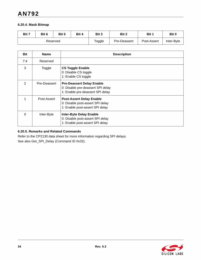
6.20.4. Mask Bitmap
6.20.5. Remarks and Related Commands
Refer to the CP2130 data sheet for more information regarding SPI delays.
See also Get_SPI_Delay (Command ID 0x32).
Bit 7 Bit 6 Bit 5 Bit 4 Bit 3 Bit 2 Bit 1 Bit 0
Reserved Toggle Pre-Deassert Post-Assert Inter-Byte
Bit Name Description
7:4 Reserved
3 Toggle CS Toggle Enable0: Disable CS toggle1: Enable CS toggle
2 Pre-Deassert Pre-Deassert Delay Enable0: Disable pre-deassert SPI delay1: Enable pre-deassert SPI delay
1 Post-Assert Post-Assert Delay Enable0: Disable post-assert SPI delay1: Enable post-assert SPI delay
0 Inter-Byte Inter-Byte Delay Enable0: Disable post-assert SPI delay1: Enable post-assert SPI delay

AN792
Rev. 0.3 35
7. OTP ROM Configuration Commands (Control Transfers)
OTP ROM stores configuration options that are persistent across power-on reset and all other resets. After reset,the CP2130 configures parameters according to values programmed in the OTP ROM. After OTP settings areinitialized, runtime parameters may be then be configured, altering the configuration of the device until the nextreset. OTP ROM configuration options can only be programmed a single time.
All CP2130 OTP ROM Configuration commands are implemented using vendor-specific control transfers on theUSB control endpoint (Endpoint 0). These commands consist of a command ID, command-dependent arguments,and return data for Get requests.
A summary of these commands is given in Table 6 with detailed descriptions in the following sections.
Table 6. OTP ROM Configuration Commands
Command Name Command ID
Comment Page
Get_Lock_Byte 0x6E Get the lock byte, which locks the specified fields to prevent them from being programmed
36
Get_Manufacturing_String_1 0x62 Get the USB manufacturing string descriptor (1 of 2) 37
Get_Manufacturing_String_2 0x64 Get the USB manufacturing string descriptor (2 of 2) 38
Get_Pin_Config 0x6C Get the pin configuration values 39
Get_Product_String_1 0x66 Get the USB product string descriptor (1 of 2) 47
Get_Product_String_2 0x68 Get the USB product string descriptor (2 of 2) 48
Get_PROM_Config 0x70 Get raw OTP ROM configuration information in blocks 49
Get_Serial_String 0x6A Get the USB serial string descriptor 50
Get_USB_Config 0x60 Get the USB configuration values 51
Set_Lock_Byte 0x6F Set the lock byte, which locks the specified fields to prevent them from being programmed
52
Set_Manufacturing_String_1 0x63 Set the USB manufacturing string descriptor (1 of 2) 53
Set_Manufacturing_String_2 0x65 Set the USB manufacturing string descriptor (2 of 2) 54
Set_Pin_Config 0x6D Set the pin configuration values 55
Set_Product_String_1 0x67 Set the USB product string descriptor (1 of 2) 63
Set_Product_String_2 0x69 Set the USB product string descriptor (2 of 2) 64
Set_PROM_Config 0x71 Set raw OTP ROM configuration information in blocks 65
Set_Serial_String 0x6B Set the USB serial string descriptor 66
Set_USB_Config 0x61 Set the USB configuration values 67

AN792
36 Rev. 0.3
7.1. Get_Lock_Byte (Command ID 0x6E)7.1.1. Description
Get the lock byte, which locks the specified fields to prevent them from being programmed.
7.1.2. Setup Stage (OUT Transfer)
7.1.3. Data Stage (IN Transfer)
7.1.4. Lock Bitmap
7.1.5. Remarks and Related Commands
Fields that are unlocked may be programmed by sending the appropriate OTP ROM Configuration command.Once a field has been programmed, the lock bit for the field is set to ‘0’, preventing future programming. Thedefault value for the field may be locked by sending this command and specifying the field as locked.
See also Set_Lock_Byte (Command ID 0x6F).
Name Value Description
bmRequestType 0xC0 Device-to-Host vendor request
bRequest 0x6E Command ID
wLength 0x0002 Data stage length in bytes
Name Offset Size Value Description
Lock 0 2 Bitmap Lock byte bitmap bit:0: Field is locked1: Field is unlocked
Offset Bit 7 Bit 6 Bit 5 Bit 4 Bit 3 Bit 2 Bit 1 Bit 0
0 TransferPriority
ManufacturingString 1
ManufacturingString 2
Release Version
Power Mode
Max Power
PID VID
1 Reserved Pin Config SerialString
Product String 2
Product String 1
AN792
Rev. 0.3 37
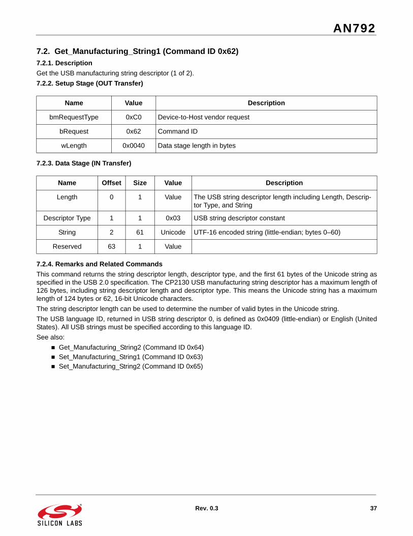
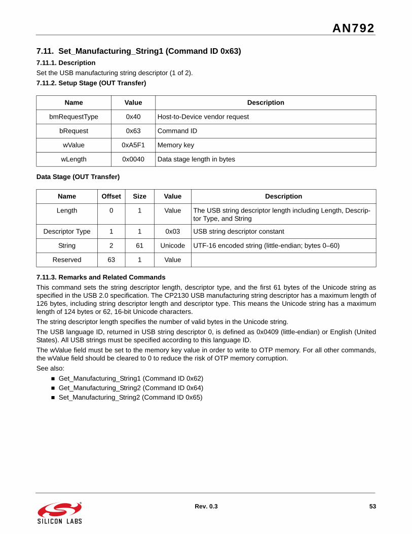
7.2. Get_Manufacturing_String1 (Command ID 0x62)7.2.1. Description
Get the USB manufacturing string descriptor (1 of 2).
7.2.2. Setup Stage (OUT Transfer)
7.2.3. Data Stage (IN Transfer)
7.2.4. Remarks and Related Commands
This command returns the string descriptor length, descriptor type, and the first 61 bytes of the Unicode string asspecified in the USB 2.0 specification. The CP2130 USB manufacturing string descriptor has a maximum length of126 bytes, including string descriptor length and descriptor type. This means the Unicode string has a maximumlength of 124 bytes or 62, 16-bit Unicode characters.
The string descriptor length can be used to determine the number of valid bytes in the Unicode string.
The USB language ID, returned in USB string descriptor 0, is defined as 0x0409 (little-endian) or English (UnitedStates). All USB strings must be specified according to this language ID.
See also:
Get_Manufacturing_String2 (Command ID 0x64)
Set_Manufacturing_String1 (Command ID 0x63)
Set_Manufacturing_String2 (Command ID 0x65)
Name Value Description
bmRequestType 0xC0 Device-to-Host vendor request
bRequest 0x62 Command ID
wLength 0x0040 Data stage length in bytes
Name Offset Size Value Description
Length 0 1 Value The USB string descriptor length including Length, Descrip-tor Type, and String
Descriptor Type 1 1 0x03 USB string descriptor constant
String 2 61 Unicode UTF-16 encoded string (little-endian; bytes 0–60)
Reserved 63 1 Value
AN792
38 Rev. 0.3
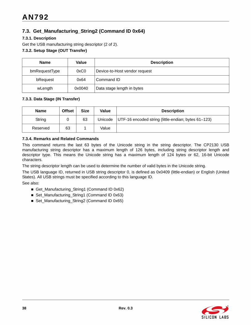
7.3. Get_Manufacturing_String2 (Command ID 0x64)7.3.1. Description
Get the USB manufacturing string descriptor (2 of 2).
7.3.2. Setup Stage (OUT Transfer)
7.3.3. Data Stage (IN Transfer)
7.3.4. Remarks and Related Commands
This command returns the last 63 bytes of the Unicode string in the string descriptor. The CP2130 USBmanufacturing string descriptor has a maximum length of 126 bytes, including string descriptor length anddescriptor type. This means the Unicode string has a maximum length of 124 bytes or 62, 16-bit Unicodecharacters.
The string descriptor length can be used to determine the number of valid bytes in the Unicode string.
The USB language ID, returned in USB string descriptor 0, is defined as 0x0409 (little-endian) or English (UnitedStates). All USB strings must be specified according to this language ID.
See also:
Get_Manufacturing_String1 (Command ID 0x62)
Set_Manufacturing_String1 (Command ID 0x63)
Set_Manufacturing_String2 (Command ID 0x65)
Name Value Description
bmRequestType 0xC0 Device-to-Host vendor request
bRequest 0x64 Command ID
wLength 0x0040 Data stage length in bytes
Name Offset Size Value Description
String 0 63 Unicode UTF-16 encoded string (little-endian; bytes 61–123)
Reserved 63 1 Value
AN792
Rev. 0.3 39
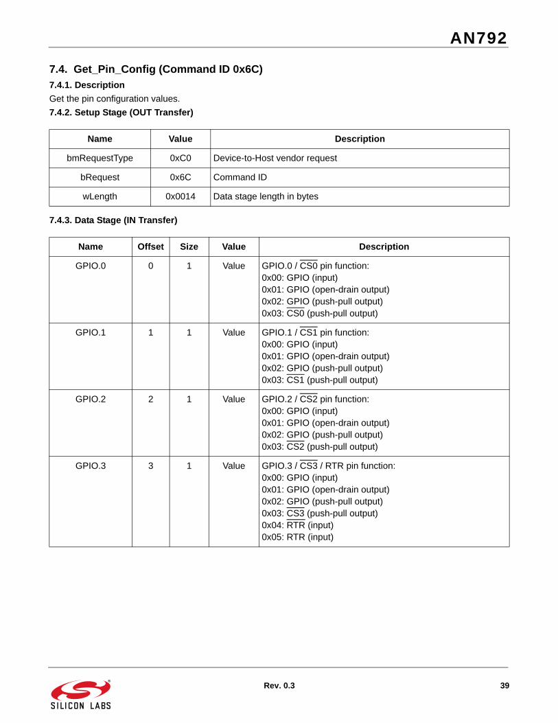
7.4. Get_Pin_Config (Command ID 0x6C)7.4.1. Description
Get the pin configuration values.
7.4.2. Setup Stage (OUT Transfer)
7.4.3. Data Stage (IN Transfer)
Name Value Description
bmRequestType 0xC0 Device-to-Host vendor request
bRequest 0x6C Command ID
wLength 0x0014 Data stage length in bytes
Name Offset Size Value Description
GPIO.0 0 1 Value GPIO.0 / CS0 pin function:0x00: GPIO (input)0x01: GPIO (open-drain output)0x02: GPIO (push-pull output)0x03: CS0 (push-pull output)
GPIO.1 1 1 Value GPIO.1 / CS1 pin function:0x00: GPIO (input)0x01: GPIO (open-drain output)0x02: GPIO (push-pull output)0x03: CS1 (push-pull output)
GPIO.2 2 1 Value GPIO.2 / CS2 pin function:0x00: GPIO (input)0x01: GPIO (open-drain output)0x02: GPIO (push-pull output)0x03: CS2 (push-pull output)
GPIO.3 3 1 Value GPIO.3 / CS3 / RTR pin function:0x00: GPIO (input)0x01: GPIO (open-drain output)0x02: GPIO (push-pull output)0x03: CS3 (push-pull output)0x04: RTR (input)0x05: RTR (input)
AN792
40 Rev. 0.3
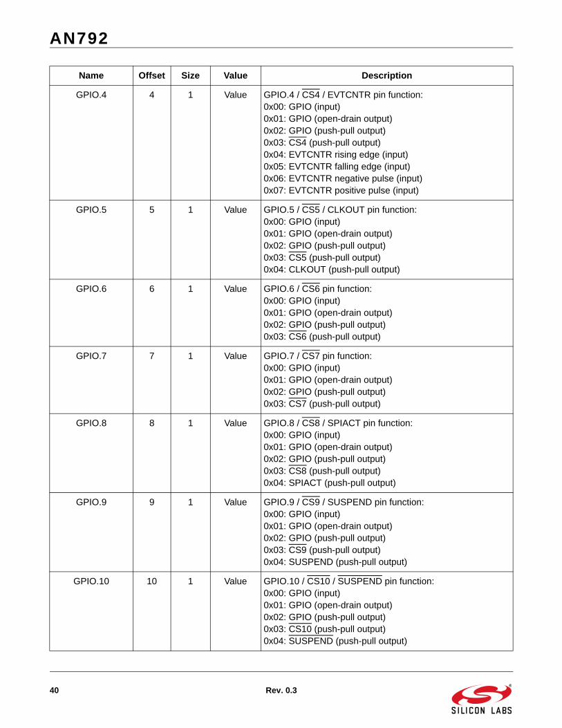
GPIO.4 4 1 Value GPIO.4 / CS4 / EVTCNTR pin function:0x00: GPIO (input)0x01: GPIO (open-drain output)0x02: GPIO (push-pull output)0x03: CS4 (push-pull output)0x04: EVTCNTR rising edge (input)0x05: EVTCNTR falling edge (input)0x06: EVTCNTR negative pulse (input)0x07: EVTCNTR positive pulse (input)
GPIO.5 5 1 Value GPIO.5 / CS5 / CLKOUT pin function:0x00: GPIO (input)0x01: GPIO (open-drain output)0x02: GPIO (push-pull output)0x03: CS5 (push-pull output)0x04: CLKOUT (push-pull output)
GPIO.6 6 1 Value GPIO.6 / CS6 pin function:0x00: GPIO (input)0x01: GPIO (open-drain output)0x02: GPIO (push-pull output)0x03: CS6 (push-pull output)
GPIO.7 7 1 Value GPIO.7 / CS7 pin function:0x00: GPIO (input)0x01: GPIO (open-drain output)0x02: GPIO (push-pull output)0x03: CS7 (push-pull output)
GPIO.8 8 1 Value GPIO.8 / CS8 / SPIACT pin function:0x00: GPIO (input)0x01: GPIO (open-drain output)0x02: GPIO (push-pull output)0x03: CS8 (push-pull output)0x04: SPIACT (push-pull output)
GPIO.9 9 1 Value GPIO.9 / CS9 / SUSPEND pin function:0x00: GPIO (input)0x01: GPIO (open-drain output)0x02: GPIO (push-pull output)0x03: CS9 (push-pull output)0x04: SUSPEND (push-pull output)
GPIO.10 10 1 Value GPIO.10 / CS10 / SUSPEND pin function:0x00: GPIO (input)0x01: GPIO (open-drain output)0x02: GPIO (push-pull output)0x03: CS10 (push-pull output)0x04: SUSPEND (push-pull output)
Name Offset Size Value Description

AN792
Rev. 0.3 41
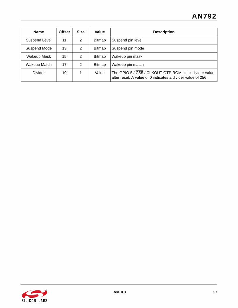
Suspend Level 11 2 Bitmap Suspend pin level
Suspend Mode 13 2 Bitmap Suspend pin mode
Wakeup Mask 15 2 Bitmap Wakeup pin mask
Wakeup Match 17 2 Bitmap Wakeup pin match
Divider 19 1 Value The GPIO.5 / CS5 / CLKOUT OTP ROM clock divider value after reset. A value of 0 indicates a divider value of 256.
Name Offset Size Value Description
AN792
42 Rev. 0.3
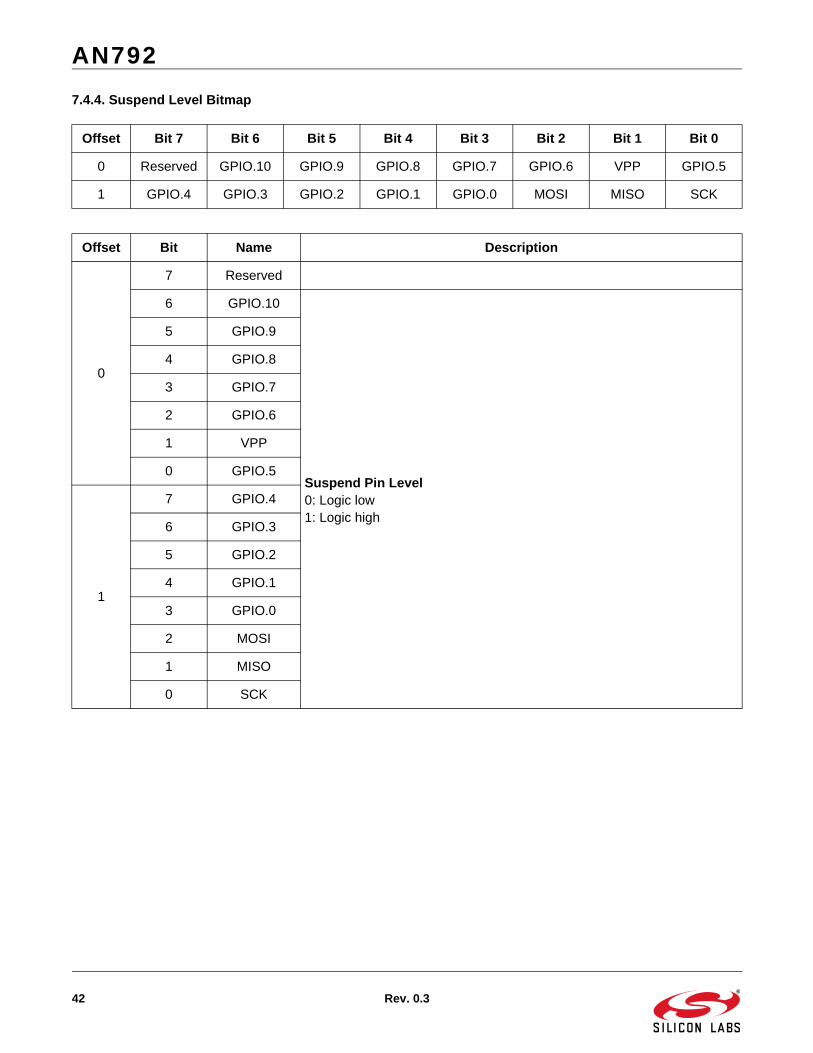
7.4.4. Suspend Level Bitmap
Offset Bit 7 Bit 6 Bit 5 Bit 4 Bit 3 Bit 2 Bit 1 Bit 0
0 Reserved GPIO.10 GPIO.9 GPIO.8 GPIO.7 GPIO.6 VPP GPIO.5
1 GPIO.4 GPIO.3 GPIO.2 GPIO.1 GPIO.0 MOSI MISO SCK
Offset Bit Name Description
0
7 Reserved
6 GPIO.10
Suspend Pin Level0: Logic low1: Logic high
5 GPIO.9
4 GPIO.8
3 GPIO.7
2 GPIO.6
1 VPP
0 GPIO.5
1
7 GPIO.4
6 GPIO.3
5 GPIO.2
4 GPIO.1
3 GPIO.0
2 MOSI
1 MISO
0 SCK

AN792
Rev. 0.3 43
7.4.5. Suspend Mode Bitmap
Offset Bit 7 Bit 6 Bit 5 Bit 4 Bit 3 Bit 2 Bit 1 Bit 0
0 Enable GPIO.10 GPIO.9 GPIO.8 GPIO.7 GPIO.6 VPP GPIO.5
1 GPIO.4 GPIO.3 GPIO.2 GPIO.1 GPIO.0 MOSI MISO SCK
Offset Bit Name Description
0
7 Enabled Suspend Mode and Level Enable0: Don’t use suspend mode and levels1: Use suspend mode and levels
6 GPIO.10
Suspend Pin Mode0: Open-drain1: Push-pull
5 GPIO.9
4 GPIO.8
3 GPIO.7
2 GPIO.6
1 VPP
0 GPIO.5
1
7 GPIO.4
6 GPIO.3
5 GPIO.2
4 GPIO.1
3 GPIO.0
2 MOSI
1 MISO
0 SCK
AN792
44 Rev. 0.3
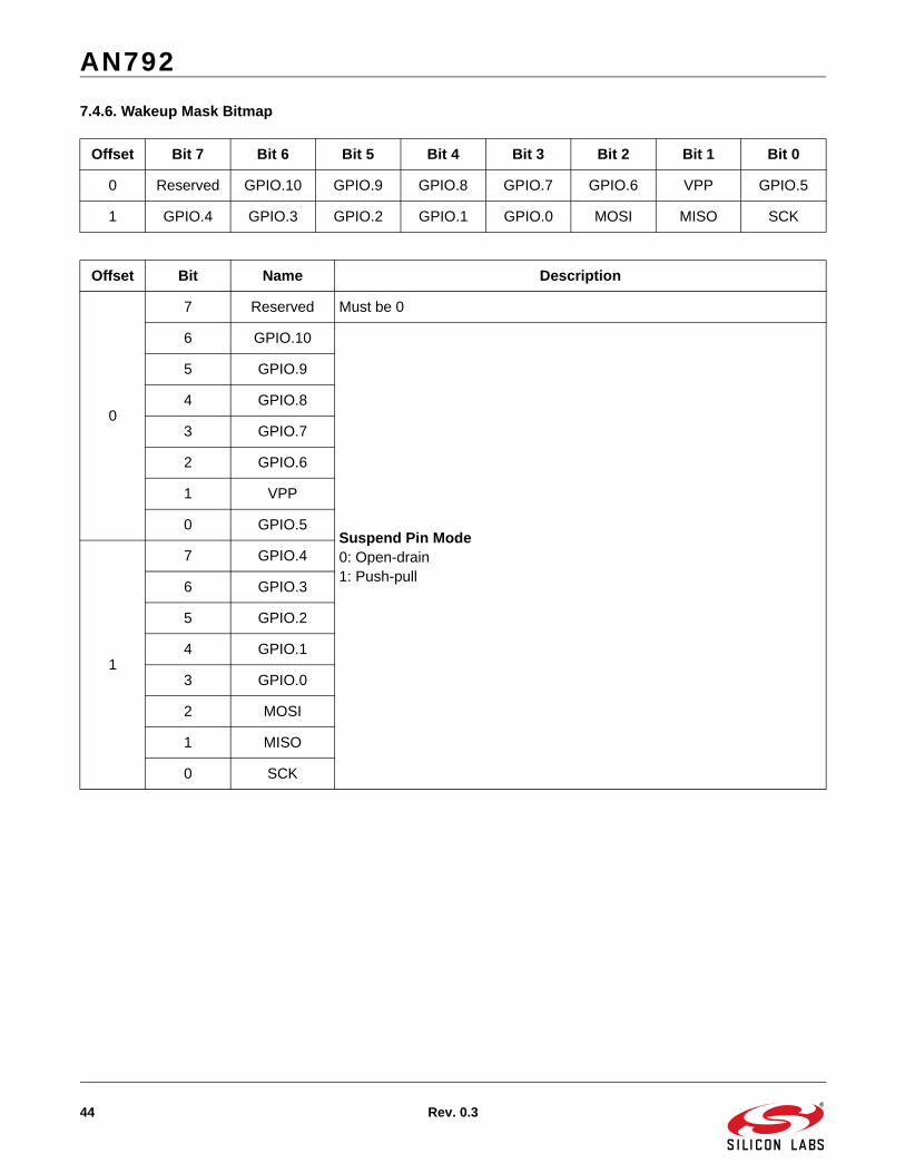
7.4.6. Wakeup Mask Bitmap
Offset Bit 7 Bit 6 Bit 5 Bit 4 Bit 3 Bit 2 Bit 1 Bit 0
0 Reserved GPIO.10 GPIO.9 GPIO.8 GPIO.7 GPIO.6 VPP GPIO.5
1 GPIO.4 GPIO.3 GPIO.2 GPIO.1 GPIO.0 MOSI MISO SCK
Offset Bit Name Description
0
7 Reserved Must be 0
6 GPIO.10
Suspend Pin Mode0: Open-drain1: Push-pull
5 GPIO.9
4 GPIO.8
3 GPIO.7
2 GPIO.6
1 VPP
0 GPIO.5
1
7 GPIO.4
6 GPIO.3
5 GPIO.2
4 GPIO.1
3 GPIO.0
2 MOSI
1 MISO
0 SCK
AN792
Rev. 0.3 45
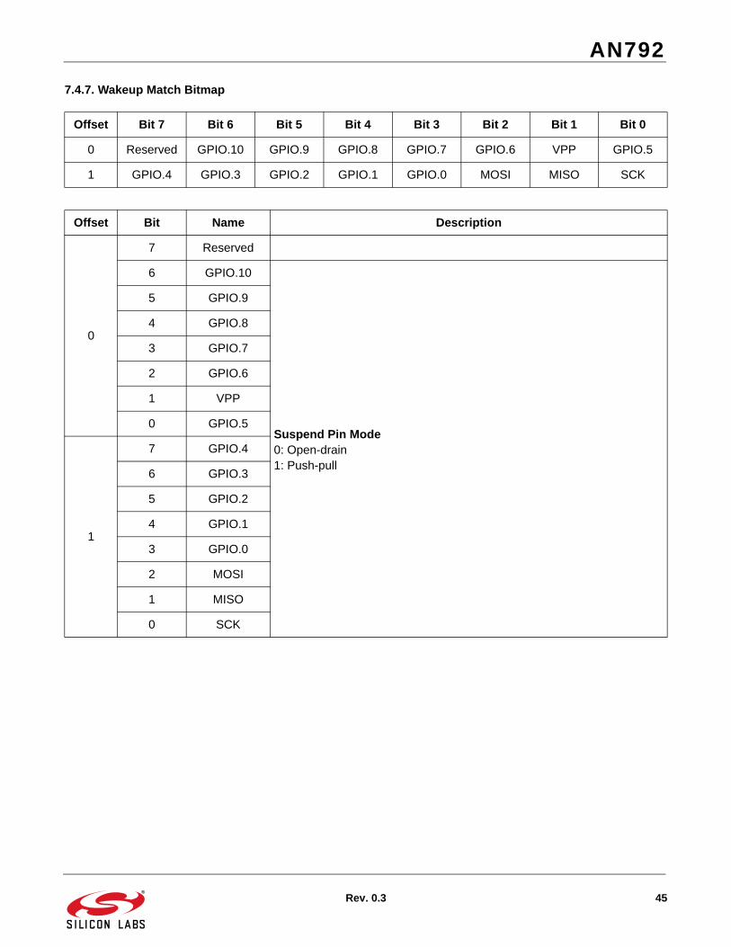
7.4.7. Wakeup Match Bitmap
Offset Bit 7 Bit 6 Bit 5 Bit 4 Bit 3 Bit 2 Bit 1 Bit 0
0 Reserved GPIO.10 GPIO.9 GPIO.8 GPIO.7 GPIO.6 VPP GPIO.5
1 GPIO.4 GPIO.3 GPIO.2 GPIO.1 GPIO.0 MOSI MISO SCK
Offset Bit Name Description
0
7 Reserved
6 GPIO.10
Suspend Pin Mode0: Open-drain1: Push-pull
5 GPIO.9
4 GPIO.8
3 GPIO.7
2 GPIO.6
1 VPP
0 GPIO.5
1
7 GPIO.4
6 GPIO.3
5 GPIO.2
4 GPIO.1
3 GPIO.0
2 MOSI
1 MISO
0 SCK
AN792
46 Rev. 0.3
7.4.8. Remarks and Related Commands
The clock divider value is used during initialization after reset. The Set_Clock_Divider (Command ID 0x47)command can be used to override the value after initialization. This command always returns the divider valuestored in the OTP ROM, not the runtime divider value. Send the Get_Clock_Divider (Command ID 0x46) commandto obtain the runtime divider value.
Any pin (GPIO.0–GPIO.10) may be used to generate a USB remote wakeup event. The wakeup mask specifieswhich pins may be used to generate a wakeup event. The wakeup match value specifies the pin values such that ifany pin selected in the wakeup mask does not match the wakeup match value, the device will generate a USBremote wakeup event when the device is suspended.
Once a GPIO pin function has been set in the OTP ROM, the pin function cannot be changed, but the output mode(push-pull or open-drain) may be overridden at runtime with the Set_GPIO_Chip_Select (Command ID 0x25) andSet_GPIO_Mode_And_Level (Command ID 0x23) commands.
Refer to the CP2130 data sheet for full pin function descriptions.
See also Set_Pin_Config (Command ID 0x6D).
AN792
Rev. 0.3 47
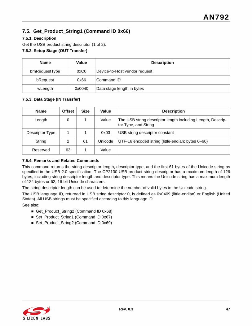
7.5. Get_Product_String1 (Command ID 0x66)7.5.1. Description
Get the USB product string descriptor (1 of 2).
7.5.2. Setup Stage (OUT Transfer)
7.5.3. Data Stage (IN Transfer)
7.5.4. Remarks and Related Commands
This command returns the string descriptor length, descriptor type, and the first 61 bytes of the Unicode string asspecified in the USB 2.0 specification. The CP2130 USB product string descriptor has a maximum length of 126bytes, including string descriptor length and descriptor type. This means the Unicode string has a maximum lengthof 124 bytes or 62, 16-bit Unicode characters.
The string descriptor length can be used to determine the number of valid bytes in the Unicode string.
The USB language ID, returned in USB string descriptor 0, is defined as 0x0409 (little-endian) or English (UnitedStates). All USB strings must be specified according to this language ID.
See also:
Get_Product_String2 (Command ID 0x68)
Set_Product_String1 (Command ID 0x67)
Set_Product_String2 (Command ID 0x69)
Name Value Description
bmRequestType 0xC0 Device-to-Host vendor request
bRequest 0x66 Command ID
wLength 0x0040 Data stage length in bytes
Name Offset Size Value Description
Length 0 1 Value The USB string descriptor length including Length, Descrip-tor Type, and String
Descriptor Type 1 1 0x03 USB string descriptor constant
String 2 61 Unicode UTF-16 encoded string (little-endian; bytes 0–60)
Reserved 63 1 Value

AN792
48 Rev. 0.3
7.6. Get_Product_String2 (Command ID 0x68)7.6.1. Description
Get the USB product string descriptor (2 of 2).
7.6.2. Setup Stage (OUT Transfer)
7.6.3. Data Stage (IN Transfer)
7.6.4. Remarks and Related Commands
This command returns the last 63 bytes of the Unicode string in the string descriptor. The CP2130 USB productstring descriptor has a maximum length of 126 bytes, including string descriptor length and descriptor type. Thismeans the Unicode string has a maximum length of 124 bytes or 62, 16-bit Unicode characters.
The string descriptor length can be used to determine the number of valid bytes in the Unicode string.
The USB language ID, returned in USB string descriptor 0, is defined as 0x0409 (little-endian) or English (UnitedStates). All USB strings must be specified according to this language ID.
See also:
Get_Product_String1 (Command ID 0x66)
Set_Product_String1 (Command ID 0x67)
Set_Product_String2 (Command ID 0x69)
Name Value Description
bmRequestType 0xC0 Device-to-Host vendor request
bRequest 0x68 Command ID
wLength 0x0040 Data stage length in bytes
Name Offset Size Value Description
String 0 63 Unicode UTF-16 encoded string (little-endian; bytes 61–123)
Reserved 63 1 Value
AN792
Rev. 0.3 49
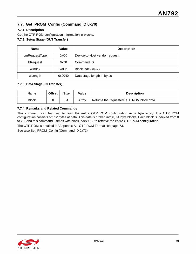
7.7. Get_PROM_Config (Command ID 0x70)7.7.1. Description
Get the OTP ROM configuration information in blocks.
7.7.2. Setup Stage (OUT Transfer)
7.7.3. Data Stage (IN Transfer)
7.7.4. Remarks and Related Commands
This command can be used to read the entire OTP ROM configuration as a byte array. The OTP ROMconfiguration consists of 512 bytes of data. This data is broken into 8, 64-byte blocks. Each block is indexed from 0to 7. Send this command 8 times with block index 0–7 to retrieve the entire OTP ROM configuration.
The OTP ROM is detailed in "Appendix A—OTP ROM Format" on page 73.
See also Set_PROM_Config (Command ID 0x71).
Name Value Description
bmRequestType 0xC0 Device-to-Host vendor request
bRequest 0x70 Command ID
wIndex Value Block index (0–7).
wLength 0x0040 Data stage length in bytes
Name Offset Size Value Description
Block 0 64 Array Returns the requested OTP ROM block data

AN792
50 Rev. 0.3
7.8. Get_Serial_String (Command ID 0x6A)7.8.1. Description
Get the USB serial string descriptor.
7.8.2. Setup Stage (OUT Transfer)
7.8.3. Data Stage (IN Transfer)
7.8.4. Remarks and Related Commands
This command returns the string descriptor length, descriptor type, and 60 bytes of the Unicode string as specifiedin the USB 2.0 specification. The CP2130 USB serial string descriptor has a maximum length of 62 bytes, includingstring descriptor length and descriptor type. This means the Unicode string has a maximum length of 60 bytes or30, 16-bit Unicode characters.
The string descriptor length can be used to determine the number of valid bytes in the Unicode string.
The USB language ID, returned in USB string descriptor 0, is defined as 0x0409 (little-endian) or English (UnitedStates). All USB strings must be specified according to this language ID.
See also Set_Serial_String (Command ID 0x6B).
Name Value Description
bmRequestType 0xC0 Device-to-Host vendor request
bRequest 0x6A Command ID
wLength 0x0040 Data stage length in bytes
Name Offset Size Value Description
Length 0 1 Value The USB string descriptor length including Length, Descrip-tor Type, and String
Descriptor Type 1 1 0x03 USB string descriptor constant
String 2 60 Unicode UTF-16 encoded string (little-endian; bytes 0–59)
Reserved 62 2 Value
AN792
Rev. 0.3 51
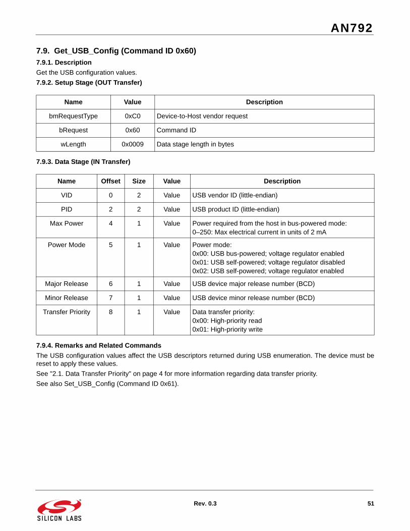
7.9. Get_USB_Config (Command ID 0x60)7.9.1. Description
Get the USB configuration values.
7.9.2. Setup Stage (OUT Transfer)
7.9.3. Data Stage (IN Transfer)
7.9.4. Remarks and Related Commands
The USB configuration values affect the USB descriptors returned during USB enumeration. The device must bereset to apply these values.
See "2.1. Data Transfer Priority" on page 4 for more information regarding data transfer priority.
See also Set_USB_Config (Command ID 0x61).
Name Value Description
bmRequestType 0xC0 Device-to-Host vendor request
bRequest 0x60 Command ID
wLength 0x0009 Data stage length in bytes
Name Offset Size Value Description
VID 0 2 Value USB vendor ID (little-endian)
PID 2 2 Value USB product ID (little-endian)
Max Power 4 1 Value Power required from the host in bus-powered mode:0–250: Max electrical current in units of 2 mA
Power Mode 5 1 Value Power mode:0x00: USB bus-powered; voltage regulator enabled0x01: USB self-powered; voltage regulator disabled0x02: USB self-powered; voltage regulator enabled
Major Release 6 1 Value USB device major release number (BCD)
Minor Release 7 1 Value USB device minor release number (BCD)
Transfer Priority 8 1 Value Data transfer priority:0x00: High-priority read0x01: High-priority write
AN792
52 Rev. 0.3
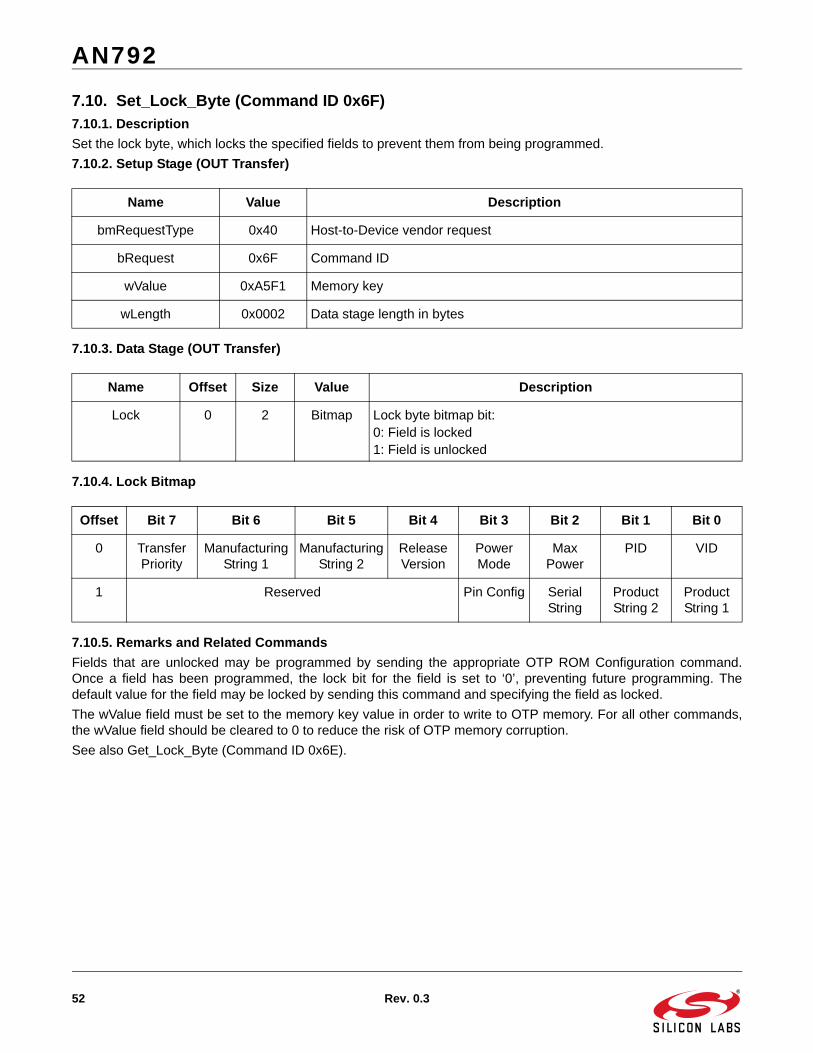
7.10. Set_Lock_Byte (Command ID 0x6F)7.10.1. Description
Set the lock byte, which locks the specified fields to prevent them from being programmed.
7.10.2. Setup Stage (OUT Transfer)
7.10.3. Data Stage (OUT Transfer)
7.10.4. Lock Bitmap
7.10.5. Remarks and Related Commands
Fields that are unlocked may be programmed by sending the appropriate OTP ROM Configuration command.Once a field has been programmed, the lock bit for the field is set to ‘0’, preventing future programming. Thedefault value for the field may be locked by sending this command and specifying the field as locked.
The wValue field must be set to the memory key value in order to write to OTP memory. For all other commands,the wValue field should be cleared to 0 to reduce the risk of OTP memory corruption.
See also Get_Lock_Byte (Command ID 0x6E).
Name Value Description
bmRequestType 0x40 Host-to-Device vendor request
bRequest 0x6F Command ID
wValue 0xA5F1 Memory key
wLength 0x0002 Data stage length in bytes
Name Offset Size Value Description
Lock 0 2 Bitmap Lock byte bitmap bit:0: Field is locked1: Field is unlocked
Offset Bit 7 Bit 6 Bit 5 Bit 4 Bit 3 Bit 2 Bit 1 Bit 0
0 TransferPriority
ManufacturingString 1
ManufacturingString 2
Release Version
Power Mode
Max Power
PID VID
1 Reserved Pin Config SerialString
Product String 2
Product String 1
AN792
Rev. 0.3 53
7.11. Set_Manufacturing_String1 (Command ID 0x63)7.11.1. Description
Set the USB manufacturing string descriptor (1 of 2).
7.11.2. Setup Stage (OUT Transfer)
Data Stage (OUT Transfer)
7.11.3. Remarks and Related Commands
This command sets the string descriptor length, descriptor type, and the first 61 bytes of the Unicode string asspecified in the USB 2.0 specification. The CP2130 USB manufacturing string descriptor has a maximum length of126 bytes, including string descriptor length and descriptor type. This means the Unicode string has a maximumlength of 124 bytes or 62, 16-bit Unicode characters.
The string descriptor length specifies the number of valid bytes in the Unicode string.
The USB language ID, returned in USB string descriptor 0, is defined as 0x0409 (little-endian) or English (UnitedStates). All USB strings must be specified according to this language ID.
The wValue field must be set to the memory key value in order to write to OTP memory. For all other commands,the wValue field should be cleared to 0 to reduce the risk of OTP memory corruption.
See also:
Get_Manufacturing_String1 (Command ID 0x62)
Get_Manufacturing_String2 (Command ID 0x64)
Set_Manufacturing_String2 (Command ID 0x65)
Name Value Description
bmRequestType 0x40 Host-to-Device vendor request
bRequest 0x63 Command ID
wValue 0xA5F1 Memory key
wLength 0x0040 Data stage length in bytes
Name Offset Size Value Description
Length 0 1 Value The USB string descriptor length including Length, Descrip-tor Type, and String
Descriptor Type 1 1 0x03 USB string descriptor constant
String 2 61 Unicode UTF-16 encoded string (little-endian; bytes 0–60)
Reserved 63 1 Value

AN792
54 Rev. 0.3
7.12. Set_Manufacturing_String2 (Command ID 0x65)7.12.1. Description
Set the USB manufacturing string descriptor (2 of 2).
7.12.2. Setup Stage (OUT Transfer)
7.12.3. Data Stage (OUT Transfer)
7.12.4. Remarks and Related Commands
This command sets the last 63 bytes of the Unicode string in the string descriptor. The CP2130 USB manufacturingstring descriptor has a maximum length of 126 bytes, including string descriptor length and descriptor type. Thismeans the Unicode string has a maximum length of 124 bytes or 62, 16-bit Unicode characters.
The string descriptor length specifies the number of valid bytes in the Unicode string.
The USB language ID, returned in USB string descriptor 0, is defined as 0x0409 (little-endian) or English (UnitedStates). All USB strings must be specified according to this language ID.
The wValue field must be set to the memory key value in order to write to OTP memory. For all other commands,the wValue field should be cleared to 0 to reduce the risk of OTP memory corruption.
See also:
Get_Manufacturing_String1 (Command ID 0x62)
Get_Manufacturing_String2 (Command ID 0x64)
Set_Manufacturing_String1 (Command ID 0x63)
Name Value Description
bmRequestType 0x40 Host-to-Device vendor request
bRequest 0x65 Command ID
wValue 0xA5F1 Memory key
wLength 0x0040 Data stage length in bytes
Name Offset Size Value Description
String 0 63 Unicode UTF-16 encoded string (little-endian; bytes 61–123)
Reserved 63 1 Value
AN792
Rev. 0.3 55
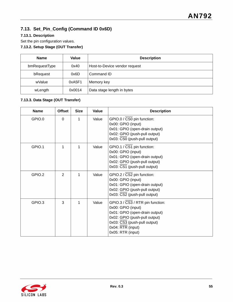
7.13. Set_Pin_Config (Command ID 0x6D)7.13.1. Description
Set the pin configuration values.
7.13.2. Setup Stage (OUT Transfer)
7.13.3. Data Stage (OUT Transfer)
Name Value Description
bmRequestType 0x40 Host-to-Device vendor request
bRequest 0x6D Command ID
wValue 0xA5F1 Memory key
wLength 0x0014 Data stage length in bytes
Name Offset Size Value Description
GPIO.0 0 1 Value GPIO.0 / CS0 pin function:0x00: GPIO (input)0x01: GPIO (open-drain output)0x02: GPIO (push-pull output)0x03: CS0 (push-pull output)
GPIO.1 1 1 Value GPIO.1 / CS1 pin function:0x00: GPIO (input)0x01: GPIO (open-drain output)0x02: GPIO (push-pull output)0x03: CS1 (push-pull output)
GPIO.2 2 1 Value GPIO.2 / CS2 pin function:0x00: GPIO (input)0x01: GPIO (open-drain output)0x02: GPIO (push-pull output)0x03: CS2 (push-pull output)
GPIO.3 3 1 Value GPIO.3 / CS3 / RTR pin function:0x00: GPIO (input)0x01: GPIO (open-drain output)0x02: GPIO (push-pull output)0x03: CS3 (push-pull output)0x04: RTR (input)0x05: RTR (input)

AN792
56 Rev. 0.3
GPIO.4 4 1 Value GPIO.4 / CS4 / EVTCNTR pin function:0x00: GPIO (input)0x01: GPIO (open-drain output)0x02: GPIO (push-pull output)0x03: CS4 (push-pull output)0x04: EVTCNTR rising edge (input)0x05: EVTCNTR falling edge (input)0x06: EVTCNTR negative pulse (input)0x07: EVTCNTR positive pulse (input)
GPIO.5 5 1 Value GPIO.5 / CS5 / CLKOUT pin function:0x00: GPIO (input)0x01: GPIO (open-drain output)0x02: GPIO (push-pull output)0x03: CS5 (push-pull output)0x04: CLKOUT (push-pull output)
GPIO.6 6 1 Value GPIO.6 / CS6 pin function:0x00: GPIO (input)0x01: GPIO (open-drain output)0x02: GPIO (push-pull output)0x03: CS6 (push-pull output)
GPIO.7 7 1 Value GPIO.7 / CS7 pin function:0x00: GPIO (input)0x01: GPIO (open-drain output)0x02: GPIO (push-pull output)0x03: CS7 (push-pull output)
GPIO.8 8 1 Value GPIO.8 / CS8 / SPIACT pin function:0x00: GPIO (input)0x01: GPIO (open-drain output)0x02: GPIO (push-pull output)0x03: CS8 (push-pull output)0x04: SPIACT (push-pull output)
GPIO.9 9 1 Value GPIO.9 / CS9 / SUSPEND pin function:0x00: GPIO (input)0x01: GPIO (open-drain output)0x02: GPIO (push-pull output)0x03: CS9 (push-pull output)0x04: SUSPEND (push-pull output)
GPIO.10 10 1 Value GPIO.10 / CS10 / SUSPEND pin function:0x00: GPIO (input)0x01: GPIO (open-drain output)0x02: GPIO (push-pull output)0x03: CS10 (push-pull output)0x04: SUSPEND (push-pull output)
Name Offset Size Value Description
AN792
Rev. 0.3 57
Suspend Level 11 2 Bitmap Suspend pin level
Suspend Mode 13 2 Bitmap Suspend pin mode
Wakeup Mask 15 2 Bitmap Wakeup pin mask
Wakeup Match 17 2 Bitmap Wakeup pin match
Divider 19 1 Value The GPIO.5 / CS5 / CLKOUT OTP ROM clock divider value after reset. A value of 0 indicates a divider value of 256.
Name Offset Size Value Description

AN792
58 Rev. 0.3
7.13.4. Suspend Level Bitmap
Offset Bit 7 Bit 6 Bit 5 Bit 4 Bit 3 Bit 2 Bit 1 Bit 0
0 Reserved GPIO.10 GPIO.9 GPIO.8 GPIO.7 GPIO.6 VPP GPIO.5
1 GPIO.4 GPIO.3 GPIO.2 GPIO.1 GPIO.0 MOSI MISO SCK
Offset Bit Name Description
0
7 Reserved
6 GPIO.10
Suspend Pin Level0: Logic low1: Logic high
5 GPIO.9
4 GPIO.8
3 GPIO.7
2 GPIO.6
1 VPP
0 GPIO.5
1
7 GPIO.4
6 GPIO.3
5 GPIO.2
4 GPIO.1
3 GPIO.0
2 MOSI
1 MISO
0 SCK
AN792
Rev. 0.3 59
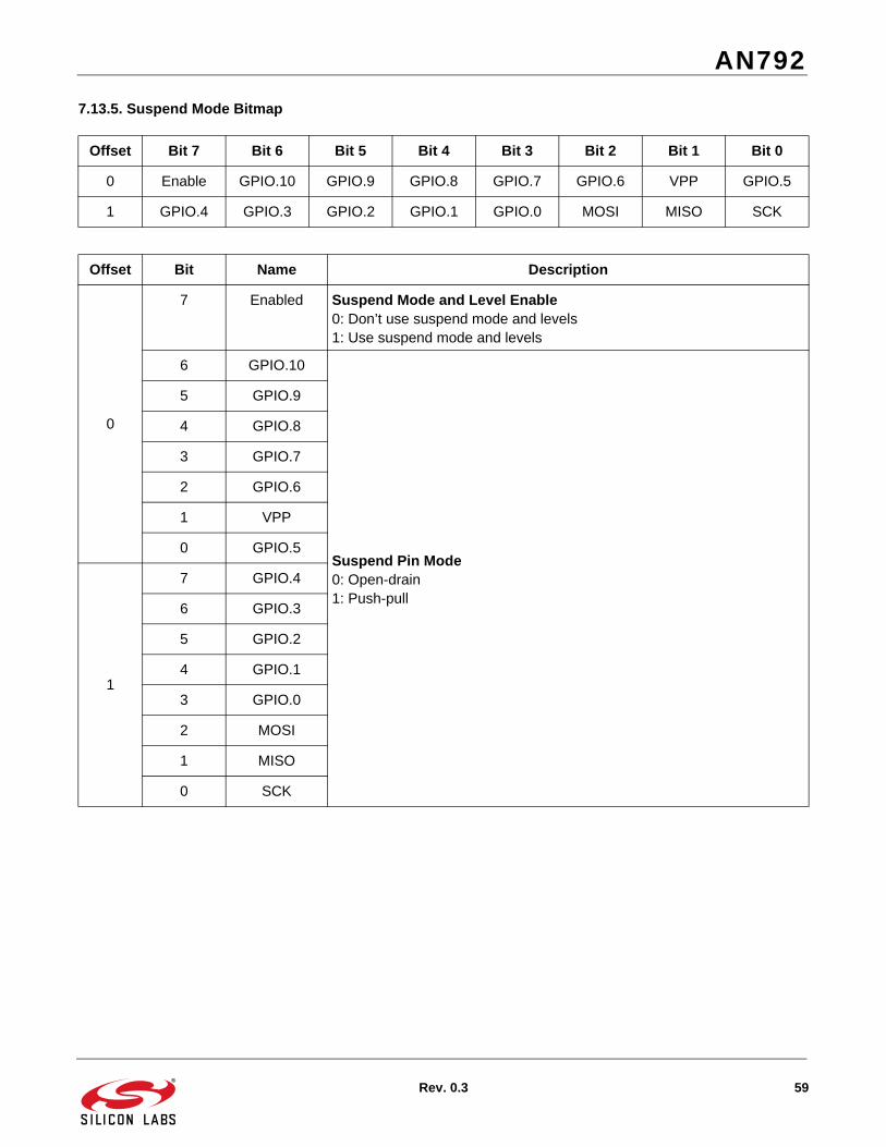
7.13.5. Suspend Mode Bitmap
Offset Bit 7 Bit 6 Bit 5 Bit 4 Bit 3 Bit 2 Bit 1 Bit 0
0 Enable GPIO.10 GPIO.9 GPIO.8 GPIO.7 GPIO.6 VPP GPIO.5
1 GPIO.4 GPIO.3 GPIO.2 GPIO.1 GPIO.0 MOSI MISO SCK
Offset Bit Name Description
0
7 Enabled Suspend Mode and Level Enable0: Don’t use suspend mode and levels1: Use suspend mode and levels
6 GPIO.10
Suspend Pin Mode0: Open-drain1: Push-pull
5 GPIO.9
4 GPIO.8
3 GPIO.7
2 GPIO.6
1 VPP
0 GPIO.5
1
7 GPIO.4
6 GPIO.3
5 GPIO.2
4 GPIO.1
3 GPIO.0
2 MOSI
1 MISO
0 SCK

AN792
60 Rev. 0.3
7.13.6. Wakeup Mask Bitmap
Offset Bit 7 Bit 6 Bit 5 Bit 4 Bit 3 Bit 2 Bit 1 Bit 0
0 Reserved GPIO.10 GPIO.9 GPIO.8 GPIO.7 GPIO.6 VPP GPIO.5
1 GPIO.4 GPIO.3 GPIO.2 GPIO.1 GPIO.0 MOSI MISO SCK
Offset Bit Name Description
0
7 Reserved Must be 0
6 GPIO.10
Suspend Pin Mode0: Open-drain1: Push-pull
5 GPIO.9
4 GPIO.8
3 GPIO.7
2 GPIO.6
1 VPP
0 GPIO.5
1
7 GPIO.4
6 GPIO.3
5 GPIO.2
4 GPIO.1
3 GPIO.0
2 MOSI
1 MISO
0 SCK

AN792
Rev. 0.3 61
7.13.7. Wakeup Match Bitmap
Offset Bit 7 Bit 6 Bit 5 Bit 4 Bit 3 Bit 2 Bit 1 Bit 0
0 Reserved GPIO.10 GPIO.9 GPIO.8 GPIO.7 GPIO.6 VPP GPIO.5
1 GPIO.4 GPIO.3 GPIO.2 GPIO.1 GPIO.0 MOSI MISO SCK
Offset Bit Name Description
0
7 Reserved
6 GPIO.10
Suspend Pin Mode0: Open-drain1: Push-pull
5 GPIO.9
4 GPIO.8
3 GPIO.7
2 GPIO.6
1 VPP
0 GPIO.5
1
7 GPIO.4
6 GPIO.3
5 GPIO.2
4 GPIO.1
3 GPIO.0
2 MOSI
1 MISO
0 SCK

AN792
62 Rev. 0.3
7.13.8. Remarks and Related Commands
The clock divider value is used during initialization after reset. The Set_Clock_Divider (Command ID 0x47)command can be used to override the value after initialization. This command always returns the divider valuestored in the OTP ROM, not the runtime divider value. Send the Get_Clock_Divider (Command ID 0x46) commandto obtain the runtime divider value.
Any pin (GPIO.0–GPIO.10) may be used to generate a USB remote wakeup event. The wakeup mask specifieswhich pins may be used to generate a wakeup event. The wakeup match value specifies the pin values such that ifany pin selected in the wakeup mask does not match the wakeup match value, the device will generate a USBremote wakeup event when the device is suspended.
Once a GPIO pin function has been set in the OTP ROM, the pin function cannot be changed, but the output mode(push-pull or open-drain) may be overridden at runtime with the Set_GPIO_Chip_Select (Command ID 0x25) andSet_GPIO_Mode_And_Level (Command ID 0x23) commands.
Refer to the CP2130 data sheet for full pin function descriptions.
The wValue field must be set to the memory key value in order to write to OTP memory. For all other commands,the wValue field should be cleared to 0 to reduce the risk of OTP memory corruption.
See also Get_Pin_Config (Command ID 0x6C).

AN792
Rev. 0.3 63
7.14. Set_Product_String1 (Command ID 0x67)7.14.1. Description
Set the USB product string descriptor (1 of 2).
7.14.2. Setup Stage (OUT Transfer)
7.14.3. Data Stage (OUT Transfer)
7.14.4. Remarks and Related Commands
This command sets the string descriptor length, descriptor type, and the first 61 bytes of the Unicode string asspecified in the USB 2.0 specification. The CP2130 USB product string descriptor has a maximum length of 126bytes, including string descriptor length and descriptor type. This means the Unicode string has a maximum lengthof 124 bytes or 62, 16-bit Unicode characters.
The string descriptor length specifies the number of valid bytes in the Unicode string.
The USB language ID, returned in USB string descriptor 0, is defined as 0x0409 (little-endian) or English (UnitedStates). All USB strings must be specified according to this language ID.
The wValue field must be set to the memory key value in order to write to OTP memory. For all other commands,the wValue field should be cleared to 0 to reduce the risk of OTP memory corruption.
See also:
Get_Product_String1 (Command ID 0x66)
Get_Product_String2 (Command ID 0x68)
Set_Product_String2 (Command ID 0x69)
Name Value Description
bmRequestType 0x40 Host-to-Device vendor request
bRequest 0x67 Command ID
wValue 0xA5F1 Memory key
wLength 0x0040 Data stage length in bytes
Name Offset Size Value Description
Length 0 1 Value The USB string descriptor length including Length, Descrip-tor Type, and String
Descriptor Type 1 1 0x03 USB string descriptor constant
String 2 61 Unicode UTF-16 encoded string (little-endian; bytes 0–60)
Reserved 63 1 Value
AN792
64 Rev. 0.3
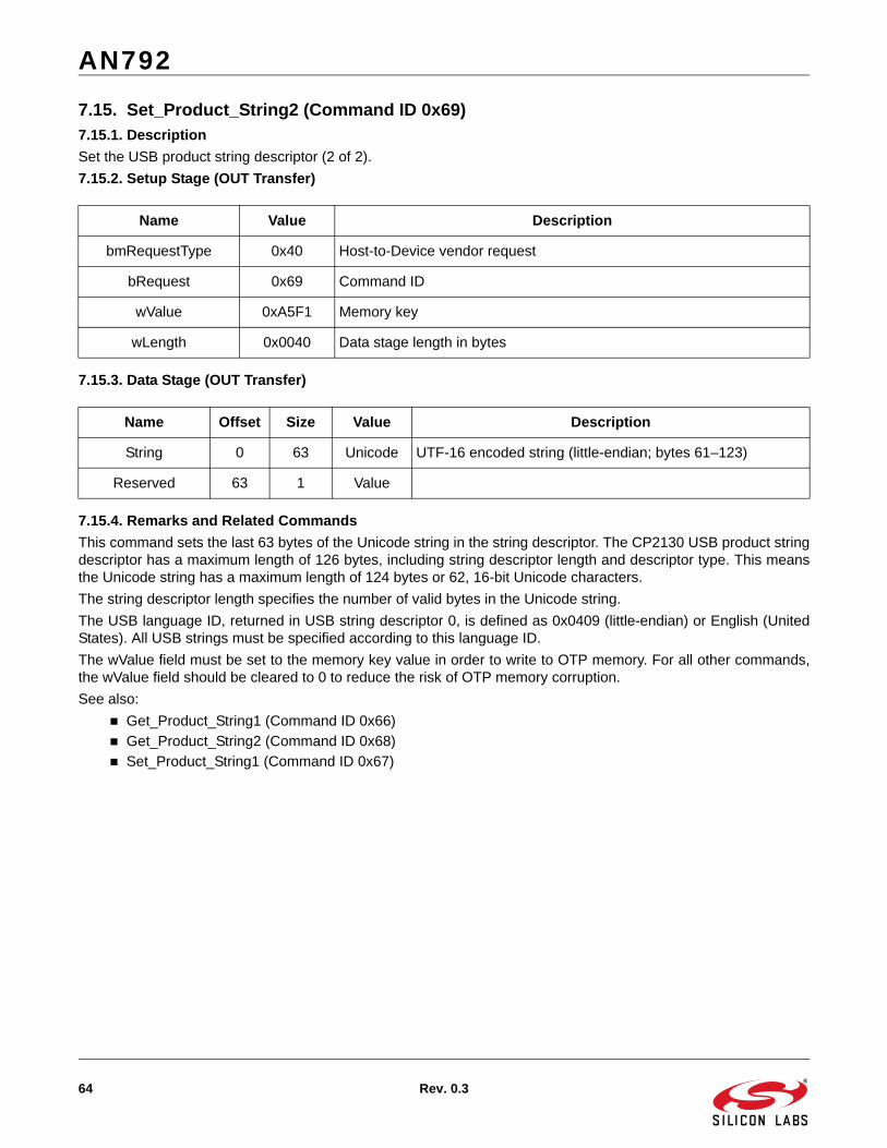
7.15. Set_Product_String2 (Command ID 0x69)7.15.1. Description
Set the USB product string descriptor (2 of 2).
7.15.2. Setup Stage (OUT Transfer)
7.15.3. Data Stage (OUT Transfer)
7.15.4. Remarks and Related Commands
This command sets the last 63 bytes of the Unicode string in the string descriptor. The CP2130 USB product stringdescriptor has a maximum length of 126 bytes, including string descriptor length and descriptor type. This meansthe Unicode string has a maximum length of 124 bytes or 62, 16-bit Unicode characters.
The string descriptor length specifies the number of valid bytes in the Unicode string.
The USB language ID, returned in USB string descriptor 0, is defined as 0x0409 (little-endian) or English (UnitedStates). All USB strings must be specified according to this language ID.
The wValue field must be set to the memory key value in order to write to OTP memory. For all other commands,the wValue field should be cleared to 0 to reduce the risk of OTP memory corruption.
See also:
Get_Product_String1 (Command ID 0x66)
Get_Product_String2 (Command ID 0x68)
Set_Product_String1 (Command ID 0x67)
Name Value Description
bmRequestType 0x40 Host-to-Device vendor request
bRequest 0x69 Command ID
wValue 0xA5F1 Memory key
wLength 0x0040 Data stage length in bytes
Name Offset Size Value Description
String 0 63 Unicode UTF-16 encoded string (little-endian; bytes 61–123)
Reserved 63 1 Value

AN792
Rev. 0.3 65
7.16. Set_PROM_Config (Command ID 0x71)7.16.1. Description
Set the OTP ROM configuration information in blocks.
7.16.2. Setup Stage (OUT Transfer)
7.16.3. Data Stage (OUT Transfer)
7.16.4. Remarks and Related Commands
This command can be used to write the entire OTP ROM configuration as a byte array. The OTP ROMconfiguration consists of 512 bytes of data. This data is broken into 8, 64-byte blocks. Each block is indexed from 0to 7. Send this command 8 times with block index 0–7 to write the entire OTP ROM configuration.
The OTP ROM is detailed in "Appendix A—OTP ROM Format" on page 73.
The wValue field must be set to the memory key value in order to write to OTP memory. For all other commands,the wValue field should be cleared to 0 to reduce the risk of OTP memory corruption.
See also Get_PROM_Config (Command ID 0x70).
Name Value Description
bmRequestType 0x40 Host-to-Device vendor request
bRequest 0x71 Command ID
wValue 0xA5F1 Memory key
wIndex Value Block index (0–7).
wLength 0x0040 Data stage length in bytes
Name Offset Size Value Description
Block 0 64 Array Writes the requested OTP ROM block data
AN792
66 Rev. 0.3
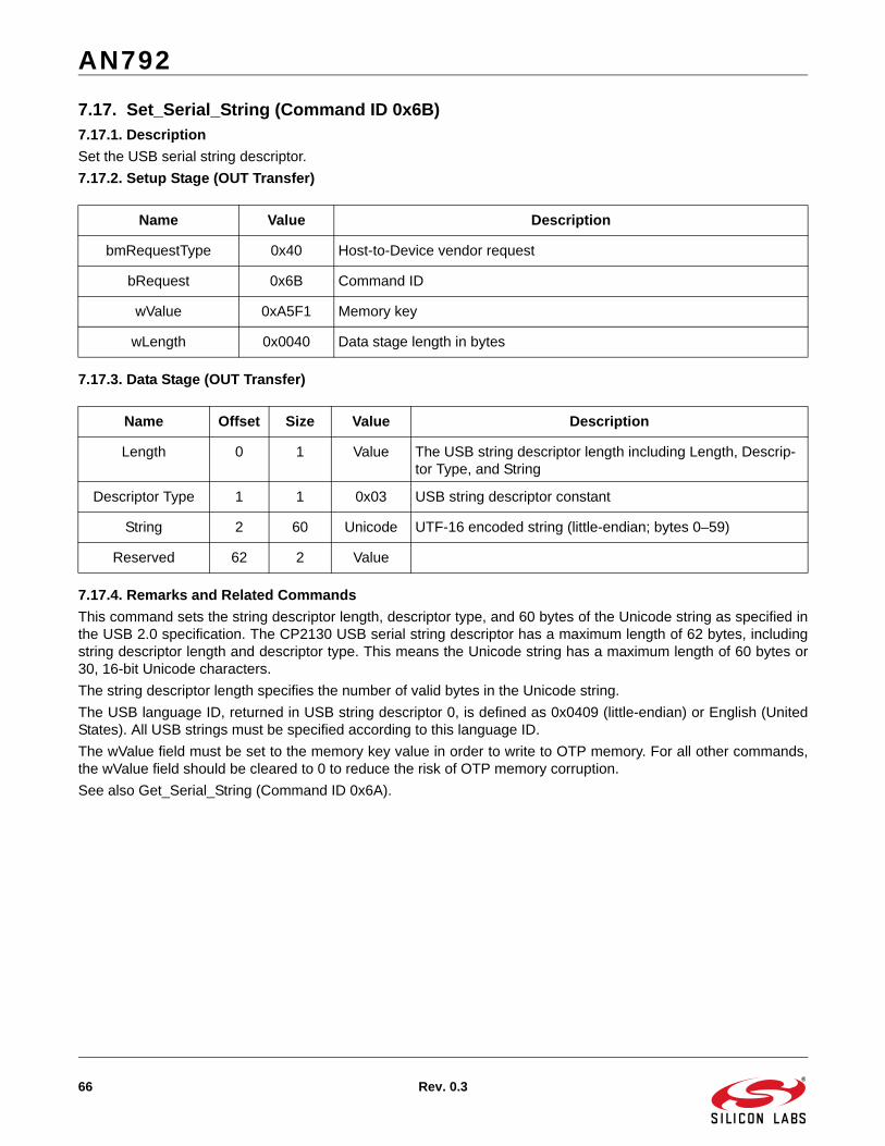
7.17. Set_Serial_String (Command ID 0x6B)7.17.1. Description
Set the USB serial string descriptor.
7.17.2. Setup Stage (OUT Transfer)
7.17.3. Data Stage (OUT Transfer)
7.17.4. Remarks and Related Commands
This command sets the string descriptor length, descriptor type, and 60 bytes of the Unicode string as specified inthe USB 2.0 specification. The CP2130 USB serial string descriptor has a maximum length of 62 bytes, includingstring descriptor length and descriptor type. This means the Unicode string has a maximum length of 60 bytes or30, 16-bit Unicode characters.
The string descriptor length specifies the number of valid bytes in the Unicode string.
The USB language ID, returned in USB string descriptor 0, is defined as 0x0409 (little-endian) or English (UnitedStates). All USB strings must be specified according to this language ID.
The wValue field must be set to the memory key value in order to write to OTP memory. For all other commands,the wValue field should be cleared to 0 to reduce the risk of OTP memory corruption.
See also Get_Serial_String (Command ID 0x6A).
Name Value Description
bmRequestType 0x40 Host-to-Device vendor request
bRequest 0x6B Command ID
wValue 0xA5F1 Memory key
wLength 0x0040 Data stage length in bytes
Name Offset Size Value Description
Length 0 1 Value The USB string descriptor length including Length, Descrip-tor Type, and String
Descriptor Type 1 1 0x03 USB string descriptor constant
String 2 60 Unicode UTF-16 encoded string (little-endian; bytes 0–59)
Reserved 62 2 Value
AN792
Rev. 0.3 67
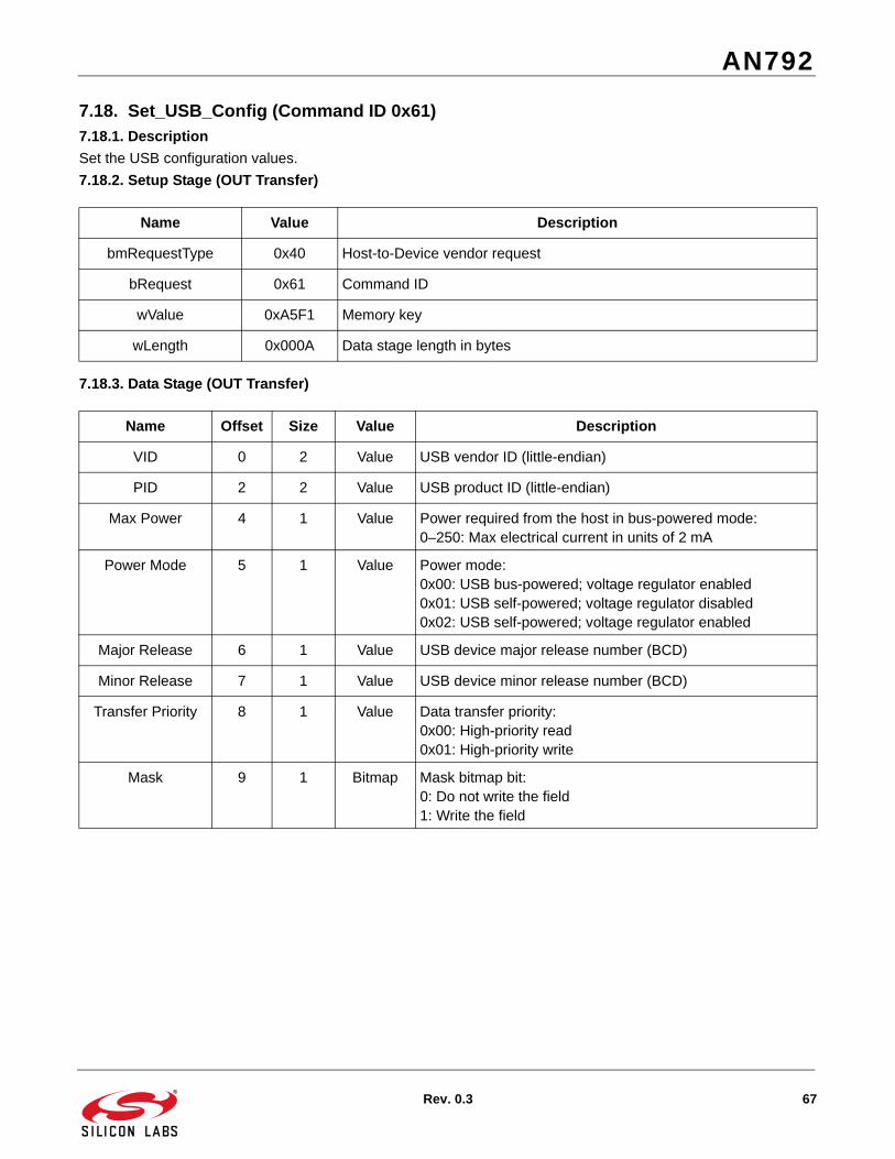
7.18. Set_USB_Config (Command ID 0x61)7.18.1. Description
Set the USB configuration values.
7.18.2. Setup Stage (OUT Transfer)
7.18.3. Data Stage (OUT Transfer)
Name Value Description
bmRequestType 0x40 Host-to-Device vendor request
bRequest 0x61 Command ID
wValue 0xA5F1 Memory key
wLength 0x000A Data stage length in bytes
Name Offset Size Value Description
VID 0 2 Value USB vendor ID (little-endian)
PID 2 2 Value USB product ID (little-endian)
Max Power 4 1 Value Power required from the host in bus-powered mode:0–250: Max electrical current in units of 2 mA
Power Mode 5 1 Value Power mode:0x00: USB bus-powered; voltage regulator enabled0x01: USB self-powered; voltage regulator disabled0x02: USB self-powered; voltage regulator enabled
Major Release 6 1 Value USB device major release number (BCD)
Minor Release 7 1 Value USB device minor release number (BCD)
Transfer Priority 8 1 Value Data transfer priority:0x00: High-priority read0x01: High-priority write
Mask 9 1 Bitmap Mask bitmap bit:0: Do not write the field1: Write the field
AN792
68 Rev. 0.3
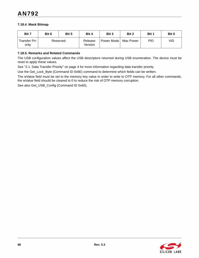
7.18.4. Mask Bitmap
7.18.5. Remarks and Related Commands
The USB configuration values affect the USB descriptors returned during USB enumeration. The device must bereset to apply these values.
See "2.1. Data Transfer Priority" on page 4 for more information regarding data transfer priority.
Use the Get_Lock_Byte (Command ID 0x6E) command to determine which fields can be written.
The wValue field must be set to the memory key value in order to write to OTP memory. For all other commands,the wValue field should be cleared to 0 to reduce the risk of OTP memory corruption.
See also Get_USB_Config (Command ID 0x60).
Bit 7 Bit 6 Bit 5 Bit 4 Bit 3 Bit 2 Bit 1 Bit 0
Transfer Pri-ority
Reserved Release Version
Power Mode Max Power PID VID
AN792
Rev. 0.3 69
8. Interfacing with the CP2130 using LibUSB
For users that are not using a Windows platform, LibUSB will be the easiest way to integrate the CP2130 with amodern host OS such as Linux or OSX. This document is accompanied by a sample C++ application that makesuse of LibUSB to show how to set GPIO values, Write and Read, from the device. This sample code should beused as an example of how to open and close the device in LibUSB and how to issue control requests to endpoint0 and bulk requests to endpoint 1 or 2.
8.1. LibUSB and LinuxThis section will show how to use LibUSB with Ubuntu 12.04. The instructions should be similar across most LinuxOS distributions. For specific installation instructions on installation and usage, visit the LibUSB website atwww.libusb.org.
8.1.1. Installation on Linux
To install the driver in Ubuntu Linux use the Advanced Packaging Tool (apt-get). This will download and place allthe files needed for LibUSB in their proper locations. Type the following command into a terminal:
sudo apt-get install libusb-1.0-0-dev
In order for a device to be accessible by non-root users a udev file needs to be created. This file is included in thesample source files which allows access to any Silicon Labs device. Place the file in /etc/udev/rules.d directory.Here is the functional part of the file:
SUBSYSTEM=="usb", ATTRS{idVendor}=="10c4", MODE="0666"SUBSYSTEM=="usb_device", ATTRS{idVendor}=="10c4", MODE="0666"
The udev file above will allow access to any Silicon Labs device because it is matching off of the VID only. Formore information and guidance on writing or customizing udev files, visit the writing page at www.reactivated.net/writing_udev_rules.html.
After performing these steps, your device can by plugged in and will be accessible via LibUSB.
8.1.2. Usage on Linux
To use LinUSB in your application you’ll need to include the proper header file and link against the LibUSBlibraries. In this C++ example, use the included libusb header file:
#include <libusb-1.0/libusb.h>
For usage in other languages, see the see the Bindings section of the bUSB website at www.libusb.org/#Bindings.
To link with the LinUSB libraries, add this command line switch to the linker:
-lusb-1.0
8.1.3. Initialization and Device Discovery
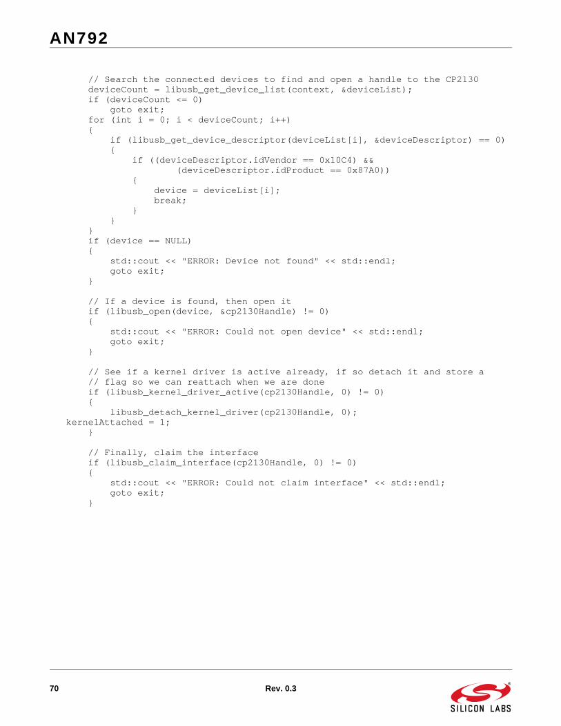
The sample application shows the calls necessary to initialize and discover a device.
The steps that need to be taken to get a handle to the CP2130 device are:
1. Initialize LibUSB using libusb_init().
2. Get the device list using libusb_get_device_list() and find a device to connect to.
3. Open the device with LibUSB using libusb_open().
4. Detach any existing kernel connection by checking libusb_kernel_driver_active() and using libusb_detach_kernel_driver() if it is connected to the kernel.
5. Claim the interface using libusb_claim_interface().
Here is the program listing from the sample application with comments for reference:
// Initialize libusb if (libusb_init(&context) != 0) goto exit;
AN792
70 Rev. 0.3
// Search the connected devices to find and open a handle to the CP2130 deviceCount = libusb_get_device_list(context, &deviceList); if (deviceCount <= 0) goto exit; for (int i = 0; i < deviceCount; i++) { if (libusb_get_device_descriptor(deviceList[i], &deviceDescriptor) == 0) { if ((deviceDescriptor.idVendor == 0x10C4) && (deviceDescriptor.idProduct == 0x87A0)) { device = deviceList[i]; break; } } } if (device == NULL) { std::cout << "ERROR: Device not found" << std::endl; goto exit; } // If a device is found, then open it if (libusb_open(device, &cp2130Handle) != 0) { std::cout << "ERROR: Could not open device" << std::endl; goto exit; } // See if a kernel driver is active already, if so detach it and store a // flag so we can reattach when we are done if (libusb_kernel_driver_active(cp2130Handle, 0) != 0) { libusb_detach_kernel_driver(cp2130Handle, 0); kernelAttached = 1; } // Finally, claim the interface if (libusb_claim_interface(cp2130Handle, 0) != 0) { std::cout << "ERROR: Could not claim interface" << std::endl; goto exit; }

AN792
Rev. 0.3 71
8.1.4. Uninitialization
The sample code also shows the calls necessary to uninitialize a device.
The steps need to be taken to disconnect from the CP2130 device are:
1. Release the interface using libusb_release_interface().
2. Reattach from the kernel using libusb_attach_kernel_driver() (only if the device was connected to the kernel previously).
3. Close the LibUSB handle using libusb_close().
4. Free the device list we obtained originaly using libusb_free_device_list().
5. Uninitialize LibUSB using libusb_exit().
Here is the program listing from the sample application for reference:
// Cleanup and deinitialize libusb if (cp2130Handle) libusb_release_interface(cp2130Handle, 0); if (kernelAttached) libusb_attach_kernel_driver(cp2130Handle, 0); if (cp2130Handle) libusb_close(cp2130Handle); if (deviceList) libusb_free_device_list(deviceList, 1); if (context) libusb_exit(context);
8.1.5. USB Requests
There are three types of USB requests that can be sent to the CP2130: control, bulk in, and bulk out. The controlrequests are used for vendor specific general purpose requests to the control endpoint. The bulk pipes will allow forreading and writing data to the SPI lines, MISO and MOSI. The sample source shows examples of each of these.
8.1.5.1. Control Requests
The example GPIO function will get/set the GPIO values with a control request. Each of the commands defined insection “6. Configuration and Control Commands (Control Transfers)” can be used with the LibUSB controlrequest function. Each of the paramaters will map to the LibUSB function. In this example we will refer to section“6.6. Get_GPIO_Values (Command ID 0x20)” .
In this command there is a bmRequestType, bRequest and wLength. In this case the other paramaters, wValueand wIndex, are set to 0. These parameters are used directly with the libusb_control_transfer_function and it willreturn the number of bytes transferred. Here is the definition:
int libusb_control_transfer(libusb_device_handle* dev_handle, uint8_tbmRequestType, uint8_t bRequest, uint16_t wValue, uint16_t wIndex, unsigned char*data, uint16_t wLength, unsigned int timeout)
After putting the defined values from section “6.6.2. Setup Stage (OUT Transfer)” in the function, this is theresulting call to get the GPIO
unsigned char control_buf_out[2];libusb_control_transfer(cp2130Handle, 0xC0, 0x20, 0x0000, 0x0000,control_buf_out, sizeof(control_buf_out), usbTimeout);
The function will return the data in the control_buf_out buffer and the return value will be 2, the size of that buffer.The GPIO values can be read form the control_buf_out buffer as defined in section “6.6.4. Level Bitmap” .
All the other requests should be formatted in the same way, according to the LibUSB documentation.
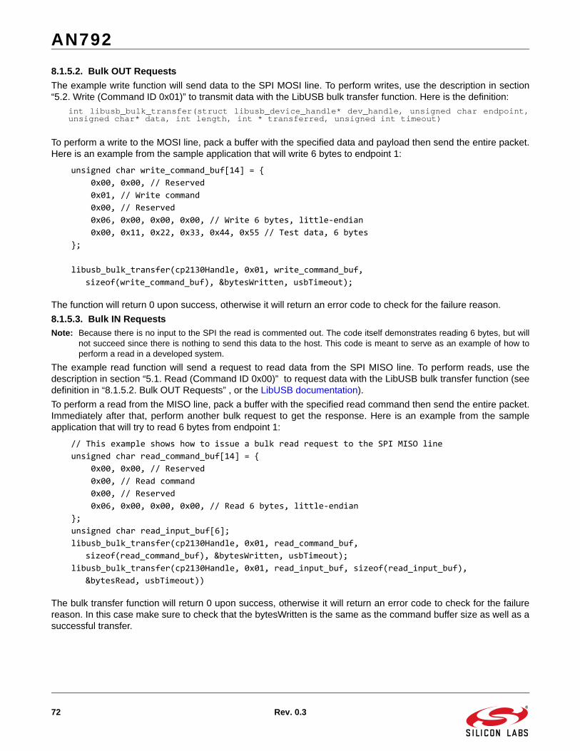
AN792
72 Rev. 0.3
8.1.5.2. Bulk OUT Requests
The example write function will send data to the SPI MOSI line. To perform writes, use the description in section“5.2. Write (Command ID 0x01)” to transmit data with the LibUSB bulk transfer function. Here is the definition:
int libusb_bulk_transfer(struct libusb_device_handle* dev_handle, unsigned char endpoint,unsigned char* data, int length, int * transferred, unsigned int timeout)
To perform a write to the MOSI line, pack a buffer with the specified data and payload then send the entire packet.Here is an example from the sample application that will write 6 bytes to endpoint 1:
unsigned char write_command_buf[14] = {
0x00, 0x00, // Reserved
0x01, // Write command
0x00, // Reserved
0x06, 0x00, 0x00, 0x00, // Write 6 bytes, little‐endian
0x00, 0x11, 0x22, 0x33, 0x44, 0x55 // Test data, 6 bytes
};
libusb_bulk_transfer(cp2130Handle, 0x01, write_command_buf,
sizeof(write_command_buf), &bytesWritten, usbTimeout);
The function will return 0 upon success, otherwise it will return an error code to check for the failure reason.
8.1.5.3. Bulk IN Requests
Note: Because there is no input to the SPI the read is commented out. The code itself demonstrates reading 6 bytes, but willnot succeed since there is nothing to send this data to the host. This code is meant to serve as an example of how toperform a read in a developed system.
The example read function will send a request to read data from the SPI MISO line. To perform reads, use thedescription in section “5.1. Read (Command ID 0x00)” to request data with the LibUSB bulk transfer function (seedefinition in “8.1.5.2. Bulk OUT Requests” , or the LibUSB documentation).
To perform a read from the MISO line, pack a buffer with the specified read command then send the entire packet.Immediately after that, perform another bulk request to get the response. Here is an example from the sampleapplication that will try to read 6 bytes from endpoint 1:
// This example shows how to issue a bulk read request to the SPI MISO line
unsigned char read_command_buf[14] = {
0x00, 0x00, // Reserved
0x00, // Read command
0x00, // Reserved
0x06, 0x00, 0x00, 0x00, // Read 6 bytes, little‐endian
};
unsigned char read_input_buf[6];
libusb_bulk_transfer(cp2130Handle, 0x01, read_command_buf,
sizeof(read_command_buf), &bytesWritten, usbTimeout);
libusb_bulk_transfer(cp2130Handle, 0x01, read_input_buf, sizeof(read_input_buf),
&bytesRead, usbTimeout))
The bulk transfer function will return 0 upon success, otherwise it will return an error code to check for the failurereason. In this case make sure to check that the bytesWritten is the same as the command buffer size as well as asuccessful transfer.
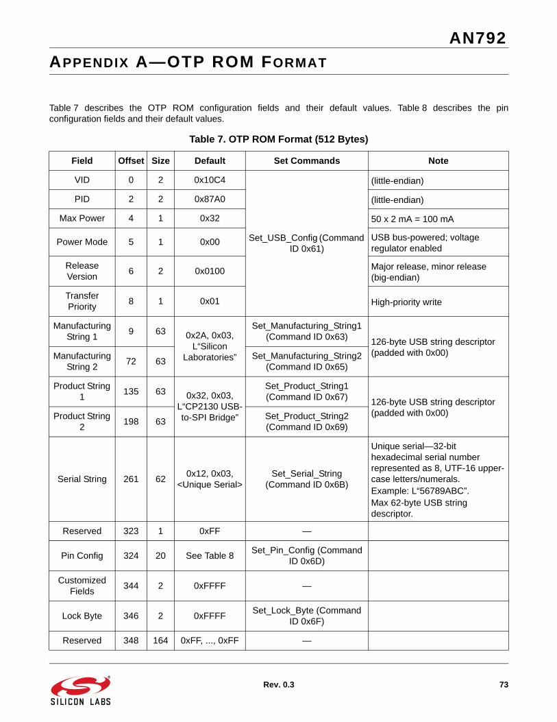
AN792
Rev. 0.3 73
APPENDIX A—OTP ROM FORMAT
Table 7 describes the OTP ROM configuration fields and their default values. Table 8 describes the pinconfiguration fields and their default values.
Table 7. OTP ROM Format (512 Bytes)
Field Offset Size Default Set Commands Note
VID 0 2 0x10C4
Set_USB_Config (Command ID 0x61)
(little-endian)
PID 2 2 0x87A0 (little-endian)
Max Power 4 1 0x32 50 x 2 mA = 100 mA
Power Mode 5 1 0x00 USB bus-powered; voltage regulator enabled
ReleaseVersion
6 2 0x0100 Major release, minor release (big-endian)
TransferPriority
8 1 0x01 High-priority write
Manufacturing String 1
9 63 0x2A, 0x03,L“Silicon
Laboratories”
Set_Manufacturing_String1 (Command ID 0x63) 126-byte USB string descriptor
(padded with 0x00)Manufacturing String 2
72 63Set_Manufacturing_String2
(Command ID 0x65)
Product String 1
135 63 0x32, 0x03, L“CP2130 USB-to-SPI Bridge”
Set_Product_String1 (Command ID 0x67) 126-byte USB string descriptor
(padded with 0x00)Product String 2
198 63Set_Product_String2 (Command ID 0x69)
Serial String 261 620x12, 0x03,
<Unique Serial>Set_Serial_String
(Command ID 0x6B)
Unique serial—32-bit hexadecimal serial number represented as 8, UTF-16 upper-case letters/numerals.Example: L“56789ABC”.Max 62-byte USB string descriptor.
Reserved 323 1 0xFF —
Pin Config 324 20 See Table 8Set_Pin_Config (Command
ID 0x6D)
Customized Fields
344 2 0xFFFF —
Lock Byte 346 2 0xFFFFSet_Lock_Byte (Command
ID 0x6F)
Reserved 348 164 0xFF, ..., 0xFF —

AN792
74 Rev. 0.3
Table 8. Pin Config Default Values (20 Bytes)
Field Default Function
GPIO.0 0x03 CS0 (push-pull output)
GPIO.1 0x03 CS1 (push-pull output)
GPIO.2 0x03 CS2 (push-pull output)
GPIO.3 0x04 RTR (input)
GPIO.4 0x04 EVTCNTR rising edge (input)
GPIO.5 0x04 CLKOUT (push-pull output)
GPIO.6 0x00 GPIO (input)
GPIO.7 0x02 GPIO (push-pull output)
GPIO.8 0x04 SPIACT (push-pull output)
GPIO.9 0x04 SUSPEND (push-pull output)
GPIO.10 0x04 SUSPEND (push-pull output)
Suspend Level 0x0000
Suspend Mode and Levels are not usedSuspend Mode
0x0000
Wakeup Mask 0x0000No pins used for wakeup
Wakeup Match 0x0000
Divider 0x00 CLKOUT = 93.75 kHz
AN792
Rev. 0.3 75
APPENDIX B—PIN CONFIGURATION OPTIONS
Some of the pins of the CP2130 are configurable as inputs, open-drain outputs, or push-pull outputs. Theseoptions are configured when the device has enumerated and is operating in a normal mode. When the CP2130 isin USB suspend, all of the configurable pins are limited to be open-drain or push-pull outputs. The followingdescribes the differences between open-drain and push-pull, and the difference in behavior in Suspend mode. Seethe CP2130 data sheet for the electrical specifications of the GPIO pins.
GPIO InputWhen a pin is configured as a GPIO input, the pin can read a logic high or logic low value. Internally, the GPIO pin is connected to the VIO pin through a resistor. If the pin is not connected externally, it will return a logic high or 1. Any voltages connected to the pin should conform to data sheet specifications.
Open-Drain OutputWhen a pin is configured as a GPIO open-drain output, the pin can output a logic high or logic low value. The default value is logic high, and a logic high value is created by internally connecting the GPIO pin to the VIO pin through a resistor. In this mode, the pin is unable to source much current when driving a logic high. If the Set_GPIO_Mode_And_Level (Command ID 0x23) or Set_GPIO_Values (Command ID 0x21) command is used to change the output to a logic low, the pin is internally connected to GND.
Push-Pull OutputWhen a pin is configured as a GPIO push-pull output, the pin can output a logic high or logic low value. When driving a logic high value, the pin is directly connected to the VIO pin internally and can source current for devices, such as LEDs. When driving a logic low value, the pin is internally connected to GND.
Suspend ModeWhen the device is in Suspend mode, all of the GPIO pins are forced to be open-drain or push-pull outputs. The mode of each GPIO pin (open-drain or push-pull) and output value (logic-high or logic-low) is an OTP ROM configurable value which is set using the Set_Pin_Config (Command ID 0x6D) command. The modes and values of the pins during Suspend can be the same or different as when the device is in Normal mode. To maintain the same electrical characteristics of a GPIO Input Pin during Suspend, configure the pin for open-drain mode with the output latch value set to logic-high or 1.

http://www.silabs.com
Silicon Laboratories Inc.400 West Cesar ChavezAustin, TX 78701USA
Simplicity Studio
One-click access to MCU and wireless tools, documentation, software, source code libraries & more. Available for Windows, Mac and Linux!
IoT Portfoliowww.silabs.com/IoT
SW/HWwww.silabs.com/simplicity
Qualitywww.silabs.com/quality
Support and Communitycommunity.silabs.com
DisclaimerSilicon Labs intends to provide customers with the latest, accurate, and in-depth documentation of all peripherals and modules available for system and software implementers using or intending to use the Silicon Labs products. Characterization data, available modules and peripherals, memory sizes and memory addresses refer to each specific device, and "Typical" parameters provided can and do vary in different applications. Application examples described herein are for illustrative purposes only. Silicon Labs reserves the right to make changes without further notice and limitation to product information, specifications, and descriptions herein, and does not give warranties as to the accuracy or completeness of the included information. Silicon Labs shall have no liability for the consequences of use of the information supplied herein. This document does not imply or express copyright licenses granted hereunder to design or fabricate any integrated circuits. The products are not designed or authorized to be used within any Life Support System without the specific written consent of Silicon Labs. A "Life Support System" is any product or system intended to support or sustain life and/or health, which, if it fails, can be reasonably expected to result in significant personal injury or death. Silicon Labs products are not designed or authorized for military applications. Silicon Labs products shall under no circumstances be used in weapons of mass destruction including (but not limited to) nuclear, biological or chemical weapons, or missiles capable of delivering such weapons.
Trademark InformationSilicon Laboratories Inc.® , Silicon Laboratories®, Silicon Labs®, SiLabs® and the Silicon Labs logo®, Bluegiga®, Bluegiga Logo®, Clockbuilder®, CMEMS®, DSPLL®, EFM®, EFM32®, EFR, Ember®, Energy Micro, Energy Micro logo and combinations thereof, "the world’s most energy friendly microcontrollers", Ember®, EZLink®, EZRadio®, EZRadioPRO®, Gecko®, ISOmodem®, Precision32®, ProSLIC®, Simplicity Studio®, SiPHY®, Telegesis, the Telegesis Logo®, USBXpress® and others are trademarks or registered trademarks of Silicon Labs. ARM, CORTEX, Cortex-M3 and THUMB are trademarks or registered trademarks of ARM Holdings. Keil is a registered trademark of ARM Limited. All other products or brand names mentioned herein are trademarks of their respective holders.