nrf21540 · nrf21540 is an rf front-end module suitable for bluetooth low energy and ieee 802.15.4...
TRANSCRIPT
nRF21540
Objective Product Specificationv0.5.2
4446_008 v0.5.2 / 2019-12-12
Key features
Key features: Applications:
• Supports Bluetooth® Low Energy, 802.15.4, and proprietary applications
• Max output power 22 dBm
• Adjustable output power to ±1 dB from 5 to 21 dBm
• User programmable modes for TX gain
• Support for two antenna interfaces
• Receive gain +13 dB
• Single-ended 50 Ω matched input and output
• 115 mA @ +20 dBm output power
• 42 mA @ +10 dBm output power
• Control interface via IO, SPI, or a combination of both
• Supply voltage 1.7 to 3.6 V, suitable for 1.8+/-5% systems
• Operating temperature -40°C to 105°C
• Package variant QFN16 4 x 4 mm
• Smart Home applications
• Industrial and factory automation
• Asset tracking
• Advanced CE remote controls
• Sports and Fitness
• Toys
• Medical
• Beacons
4446_008 v0.5.2 ii
ContentsKey features. . . . . . . . . . . . . . . . . . . . . . . . . . . . . . . . . . . . ii
1 Revision history. . . . . . . . . . . . . . . . . . . . . . . . . . . . . . . . . 5
2 Product overview. . . . . . . . . . . . . . . . . . . . . . . . . . . . . . . . 6
3 About this document. . . . . . . . . . . . . . . . . . . . . . . . . . . . . . 73.1 Document status . . . . . . . . . . . . . . . . . . . . . . . . . . . . . . . . . 73.2 Peripheral chapters . . . . . . . . . . . . . . . . . . . . . . . . . . . . . . . . 73.3 Register tables . . . . . . . . . . . . . . . . . . . . . . . . . . . . . . . . . . 7
3.3.1 Fields and values . . . . . . . . . . . . . . . . . . . . . . . . . . . . . . . 83.3.2 Permissions . . . . . . . . . . . . . . . . . . . . . . . . . . . . . . . . . 8
3.4 Registers . . . . . . . . . . . . . . . . . . . . . . . . . . . . . . . . . . . . 83.4.1 DUMMY . . . . . . . . . . . . . . . . . . . . . . . . . . . . . . . . . . 8
4 Block diagram. . . . . . . . . . . . . . . . . . . . . . . . . . . . . . . . . 10
5 Device control. . . . . . . . . . . . . . . . . . . . . . . . . . . . . . . . . 115.1 Operational states . . . . . . . . . . . . . . . . . . . . . . . . . . . . . . . . 115.2 State transition timing . . . . . . . . . . . . . . . . . . . . . . . . . . . . . . 125.3 TX power control . . . . . . . . . . . . . . . . . . . . . . . . . . . . . . . . 135.4 UICR program usage . . . . . . . . . . . . . . . . . . . . . . . . . . . . . . . 14
6 SPI interface. . . . . . . . . . . . . . . . . . . . . . . . . . . . . . . . . . 15
7 Electrical specification. . . . . . . . . . . . . . . . . . . . . . . . . . . . . 177.1 Electrical specification . . . . . . . . . . . . . . . . . . . . . . . . . . . . . . 17
7.1.1 Current consumption . . . . . . . . . . . . . . . . . . . . . . . . . . . . 177.1.2 RX . . . . . . . . . . . . . . . . . . . . . . . . . . . . . . . . . . . . 177.1.3 TX . . . . . . . . . . . . . . . . . . . . . . . . . . . . . . . . . . . . 177.1.4 SPI timing specification . . . . . . . . . . . . . . . . . . . . . . . . . . . . 18
8 Register interface. . . . . . . . . . . . . . . . . . . . . . . . . . . . . . . 198.1 Registers . . . . . . . . . . . . . . . . . . . . . . . . . . . . . . . . . . . . 19
8.1.1 CONFREG0 . . . . . . . . . . . . . . . . . . . . . . . . . . . . . . . . . 198.1.2 CONFREG1 . . . . . . . . . . . . . . . . . . . . . . . . . . . . . . . . . 198.1.3 CONFREG2 . . . . . . . . . . . . . . . . . . . . . . . . . . . . . . . . . 208.1.4 CONFREG3 . . . . . . . . . . . . . . . . . . . . . . . . . . . . . . . . . 208.1.5 PARTNUMBER . . . . . . . . . . . . . . . . . . . . . . . . . . . . . . . . 208.1.6 HW_REVISION . . . . . . . . . . . . . . . . . . . . . . . . . . . . . . . 218.1.7 HW_ID0 . . . . . . . . . . . . . . . . . . . . . . . . . . . . . . . . . . 218.1.8 HW_ID1 . . . . . . . . . . . . . . . . . . . . . . . . . . . . . . . . . . 21
9 Hardware and layout. . . . . . . . . . . . . . . . . . . . . . . . . . . . . 229.1 Pin assignments . . . . . . . . . . . . . . . . . . . . . . . . . . . . . . . . 229.2 Reference circuitry . . . . . . . . . . . . . . . . . . . . . . . . . . . . . . . 23
10 Recommended operating conditions. . . . . . . . . . . . . . . . . . . . . 24
4446_008 v0.5.2 iii

11 Absolute maximum ratings. . . . . . . . . . . . . . . . . . . . . . . . . . 25
12 Legal notices. . . . . . . . . . . . . . . . . . . . . . . . . . . . . . . . . . 26
4446_008 v0.5.2 iv

1 Revision history
Date Version Description
Dec 2019 0.5.2 First release
4446_008 v0.5.2 5
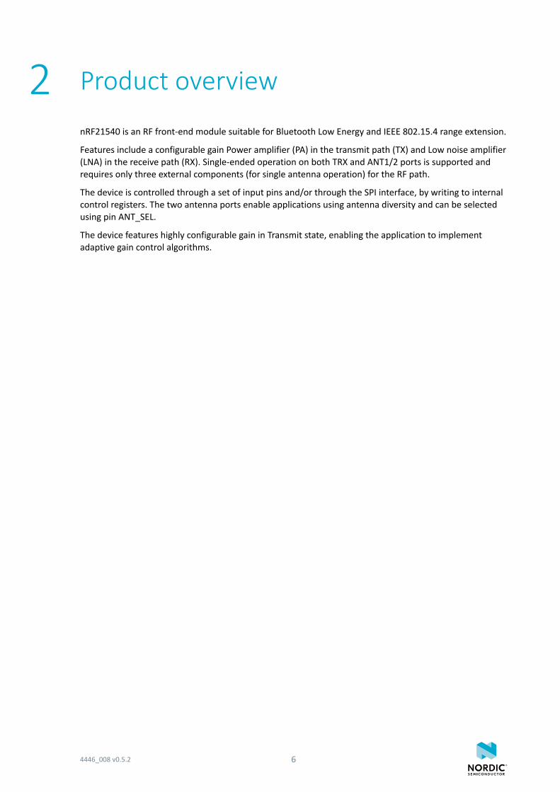
2 Product overview
nRF21540 is an RF front-end module suitable for Bluetooth Low Energy and IEEE 802.15.4 range extension.
Features include a configurable gain Power amplifier (PA) in the transmit path (TX) and Low noise amplifier(LNA) in the receive path (RX). Single-ended operation on both TRX and ANT1/2 ports is supported andrequires only three external components (for single antenna operation) for the RF path.
The device is controlled through a set of input pins and/or through the SPI interface, by writing to internalcontrol registers. The two antenna ports enable applications using antenna diversity and can be selectedusing pin ANT_SEL.
The device features highly configurable gain in Transmit state, enabling the application to implementadaptive gain control algorithms.
4446_008 v0.5.2 6
3 About this document
This document is organized into chapters that are based on the modules and peripherals available in theIC.
3.1 Document statusThe document status reflects the level of maturity of the document.
Document name Description
Objective Product Specification (OPS) Applies to document versions up to 1.0.
This document contains target specifications forproduct development.
Product Specification (PS) Applies to document versions 1.0 and higher.
This document contains final productspecifications. Nordic Semiconductor ASA reservesthe right to make changes at any time withoutnotice in order to improve design and supply thebest possible product.
Table 1: Defined document names
3.2 Peripheral chaptersEvery peripheral has a unique capitalized name or an abbreviation of its name, e.g. TIMER, used foridentification and reference. This name is used in chapter headings and references, and it will appear inthe ARM® Cortex® Microcontroller Software Interface Standard (CMSIS) hardware abstraction layer toidentify the peripheral.
The peripheral instance name, which is different from the peripheral name, is constructed using theperipheral name followed by a numbered postfix, starting with 0, for example, TIMER0. A postfix isnormally only used if a peripheral can be instantiated more than once. The peripheral instance name isalso used in the CMSIS to identify the peripheral instance.
The chapters describing peripherals may include the following information:
• A detailed functional description of the peripheral• Register configuration for the peripheral• Electrical specification tables, containing performance data which apply for the operating conditions
described in Recommended operating conditions on page 24.
3.3 Register tablesIndividual registers are described using register tables. These tables are built up of two sections. The firstthree colored rows describe the position and size of the different fields in the register. The following rowsdescribe the fields in more detail.
4446_008 v0.5.2 7
About this document
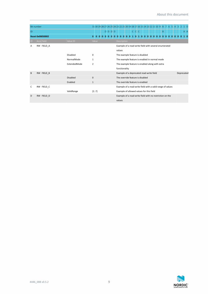
3.3.1 Fields and valuesThe Id (Field Id) row specifies the bits that belong to the different fields in the register. If a field hasenumerated values, then every value will be identified with a unique value id in the Value Id column.
A blank space means that the field is reserved and read as undefined, and it also must be written as 0to secure forward compatibility. If a register is divided into more than one field, a unique field name isspecified for each field in the Field column. The Value Id may be omitted in the single-bit bit fields whenvalues can be substituted with a Boolean type enumerator range, e.g. true/false, disable(d)/enable(d), on/off, and so on.
Values are usually provided as decimal or hexadecimal. Hexadecimal values have a 0x prefix, decimalvalues have no prefix.
The Value column can be populated in the following ways:
• Individual enumerated values, for example 1, 3, 9.• Range of values, e.g. [0..4], indicating all values from and including 0 and 4.• Implicit values. If no values are indicated in the Value column, all bit combinations are supported, or
alternatively the field's translation and limitations are described in the text instead.
If two or more fields are closely related, the Value Id, Value, and Description may be omitted for all butthe first field. Subsequent fields will indicate inheritance with '..'.
A feature marked Deprecated should not be used for new designs.
3.3.2 PermissionsDifferent fields in a register might have different access permissions enforced by hardware.
The access permission for each register field is documented in the Access column in the following ways:
Access Description Hardware behavior
RO Read-only Field can only be read. A write will be ignored.
WO Write-only Field can only be written. A read will return an undefined value.
RW Read-write Field can be read and written multiple times.
W1 Write-once Field can only be written once per reset. Any subsequent write will be ignored. A read will return an undefined value.
RW1 Read-write-once Field can be read multiple times, but only written once per reset. Any subsequent write will be ignored.
Table 2: Register field permission schemes
3.4 Registers
Register Offset Description
DUMMY 0x514 Example of a register controlling a dummy feature
Table 3: Register overview
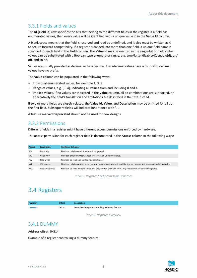
3.4.1 DUMMYAddress offset: 0x514
Example of a register controlling a dummy feature
4446_008 v0.5.2 8
About this document
Bit number 31 30 29 28 27 26 25 24 23 22 21 20 19 18 17 16 15 14 13 12 11 10 9 8 7 6 5 4 3 2 1 0
ID D D D D C C C B A A
Reset 0x00050002 0 0 0 0 0 0 0 0 0 0 0 0 0 1 0 1 0 0 0 0 0 0 0 0 0 0 0 0 0 0 1 0
ID AccessField Value ID Value Description
A RW FIELD_A Example of a read-write field with several enumerated
values
Disabled 0 The example feature is disabled
NormalMode 1 The example feature is enabled in normal mode
ExtendedMode 2 The example feature is enabled along with extra
functionality
B RW FIELD_B Example of a deprecated read-write field Deprecated
Disabled 0 The override feature is disabled
Enabled 1 The override feature is enabled
C RW FIELD_C Example of a read-write field with a valid range of values
ValidRange [2..7] Example of allowed values for this field
D RW FIELD_D Example of a read-write field with no restriction on the
values
4446_008 v0.5.2 9
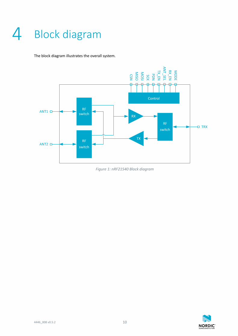
4 Block diagram
The block diagram illustrates the overall system.
RF switch
RF switch
RF switch
RX
TXANT2
ANT1
TRX
TX_ENPDNSCK
MO
DERX_EN
ANT_SEL
MO
SIM
ISOCSN
Control
Figure 1: nRF21540 Block diagram
4446_008 v0.5.2 10
5 Device control
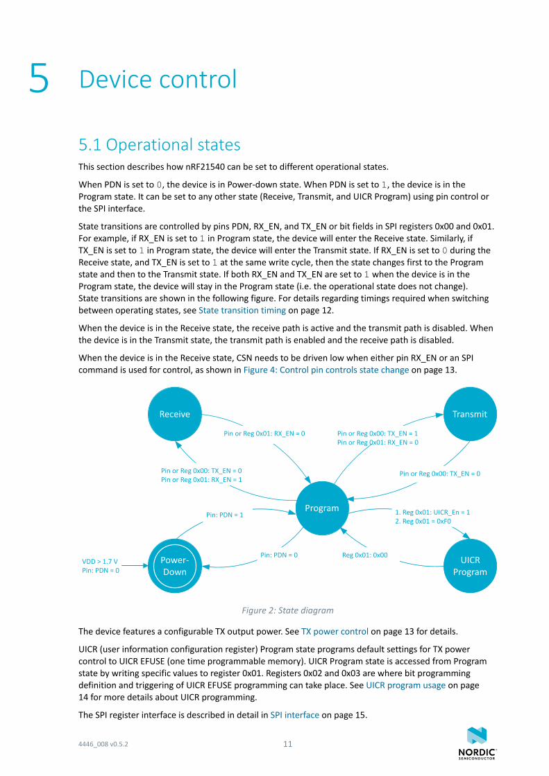
5.1 Operational statesThis section describes how nRF21540 can be set to different operational states.
When PDN is set to 0, the device is in Power-down state. When PDN is set to 1, the device is in theProgram state. It can be set to any other state (Receive, Transmit, and UICR Program) using pin control orthe SPI interface.
State transitions are controlled by pins PDN, RX_EN, and TX_EN or bit fields in SPI registers 0x00 and 0x01.For example, if RX_EN is set to 1 in Program state, the device will enter the Receive state. Similarly, ifTX_EN is set to 1 in Program state, the device will enter the Transmit state. If RX_EN is set to 0 during theReceive state, and TX_EN is set to 1 at the same write cycle, then the state changes first to the Programstate and then to the Transmit state. If both RX_EN and TX_EN are set to 1 when the device is in theProgram state, the device will stay in the Program state (i.e. the operational state does not change).State transitions are shown in the following figure. For details regarding timings required when switchingbetween operating states, see State transition timing on page 12.
When the device is in the Receive state, the receive path is active and the transmit path is disabled. Whenthe device is in the Transmit state, the transmit path is enabled and the receive path is disabled.
When the device is in the Receive state, CSN needs to be driven low when either pin RX_EN or an SPIcommand is used for control, as shown in Figure 4: Control pin controls state change on page 13.
Receive Transmit
Program
UICR Program
Pin or Reg 0x01: RX_EN = 0
Pin or Reg 0x00: TX_EN = 0
1. Reg 0x01: UICR_En = 12. Reg 0x01 = 0xF0
Reg 0x01: 0x00Pin: PDN = 0
Pin: PDN = 1
VDD > 1.7 VPin: PDN = 0
Pin or Reg 0x00: TX_EN = 1Pin or Reg 0x01: RX_EN = 0
Power-Down
Pin or Reg 0x00: TX_EN = 0 Pin or Reg 0x01: RX_EN = 1
Figure 2: State diagram
The device features a configurable TX output power. See TX power control on page 13 for details.
UICR (user information configuration register) Program state programs default settings for TX powercontrol to UICR EFUSE (one time programmable memory). UICR Program state is accessed from Programstate by writing specific values to register 0x01. Registers 0x02 and 0x03 are where bit programmingdefinition and triggering of UICR EFUSE programming can take place. See UICR program usage on page14 for more details about UICR programming.
The SPI register interface is described in detail in SPI interface on page 15.
4446_008 v0.5.2 11
Device control
State Symbol Description
Power-down PD The device is in Power-down state.
Program PG The device can be configured and set to other states.
UICR program UICR User defined initialization values for POUTA_SEL,POUTA_UICR, POUTB_SEL, and POUTB_UICR can beconfigured to UICR.
Receive RX The RX path is enabled.
Transmit TX The TX path is enabled.
Table 4: Operating states description
ANT_SEL selects which of the two antenna interfaces is used during RX or TX. Antenna interface control isspecified in Table 5: Antenna switch control with ANT_SEL in different states on page 12.
State ANT_SEL Description
Power-down X Antenna switches disabled (i.e. isolating)
Program X Antenna switches disabled (i.e. isolating)
UICR program X Antenna switches disabled (i.e. isolating)
0 ANT1 enabled, ANT2 disabledReceive
1 ANT1 disabled, ANT2 enabled
0 ANT1 enabled, ANT2 disabledTransmit
1 ANT1 disabled, ANT2 enabled
Table 5: Antenna switch control with ANT_SEL in different states
5.2 State transition timingThe following equation is used to define TPG→TRX when a slower SPI is used. Here it is assumed thatthere is a half SCK cycle gap between CSN and the first rising edge of SCK and the last falling edge of SCKand CSN.
Note: GPIO control is faster than SPI control.
Figure 3: Defining TPG to TRX with slower SPI
Settling time requirements when switching between operational states are defined in Table 6: Settlingtimes on page 13. An 8 MHz SCK clock must be used with SPI to obtain the timing given in thefollowing table.
4446_008 v0.5.2 12
Device control
Symbol Parameter Note Max. Unit
TPD→PG Settling time from state PD to PG Triggered by PDN 17.5 µs
TPG→TRX Settling time from state PG to TX orRX
Triggered by RX_EN, TX_EN, or SPIregister write
12.5 µs
TTRX→PG Power-off time when changingfrom RX or TX to PG
Triggered by RX_EN, TX_EN, or SPIReg
0x0 write
5 µs
TPG→PD Settling time from state PG to PD Triggered by PDN 10 µs
Table 6: Settling times
When the device is in the Receive state, CSN pin needs to be driven low. An example of RX timing using anRX_EN pin-based configuration is shown in the following figure.
Figure 4: Control pin controls state change
The following figure shows the Transmit state configured using SPI.
Figure 5: SPI controls state change
5.3 TX power controlThe output power for the Transmit state can be configured using either pin control or the SPI interface.
To configure the output power through pins, the MODE pin or register 0x00 can be used to set TX powercontrol to one of two preset values. Preset values are used to update the TX_Gain value when the MODEpin control changes in the Program state. Preset values can be set in UICR and selected. Table 7: TX powercontrol on page 14 presents the TX_Gain initialization functionality.
The SPI interface can also be used to control the output power. Before entering the Transmit state, TXGain is configured by writing the gain value over SPI to register 0x00 TX_Gain field. SPI write will alwaysoverwrite the initialization value. The Gain word can be set in the same write cycle when TX is enabled inthe Program state.
Note: Gain should not be changed while the device is in the Transmit state.
4446_008 v0.5.2 13
Device control
If TX_Gain is modified through SPI, and TX is not enabled (i.e. Reg 0x00: TX_EN = 0), toggling the MODEbit in Reg 0x00 will change register TX_Gain field content to preset values. If SPI write sets TX_Gain at thesame time TX_EN is set to 1, and the MODE bit in Reg 0x0 is not toggled at the same write, it does notmatter if MODE has been toggled before. The SPI written value for TX_Gain will be used in the Transmitstate. If SPI write sets the MODE bit to toggle at the same time TX_EN is set to 1, the preset TX_Gain valuewill be used in the Transmit state.
The following table shows TX power control with MODE control and corresponding preset values ofTX_Gain in program state.
MODE POUTA_SEL POUTB_SEL TX_Gain Description
0 0 X POUTA_PROD Chip production default valueused
1 X 0 POUTB_PROD Chip production default valueused
0 1 X POUTA_UICR End-user default value used
1 X 1 POUTB_UICR End-user default value used
Table 7: TX power control
5.4 UICR program usageThe UICR program state enables the automated programming sequence for UICR EFUSE cell.
The automated programming sequence can be utilized in the following manner:
1. Apply VDD supply voltage using the specifications set in the following table.
Parameter Min. Max.
VDD 3.45 V 3.60 V
TOP 0°C 85°C
Table 8: EFUSE programming conditions2. Set device to UICR Program state by sequentially writing 0x04 (UICR_EN = 1) and 0xF0 to register
CONFREG1.3. Write desired configuration values to register 0x03 for POUT_B_Sel and POUTB_UICR.4. Write desired configuration values for POUTA_Sel and POUTA_UICR to register 0x02. Write a 1 to
WR_UICR in register 0x02.5. Wait for at least 0.5 ms to guarantee successful programming.6. Reset the circuit by setting PDN to 0 and then back to 1.
The programmed values are now set for register 0x02 and 0x03. The device can be set to UICR mode forreading registers 0x02 and 0x03 to verify programmed values.
4446_008 v0.5.2 14
6 SPI interface
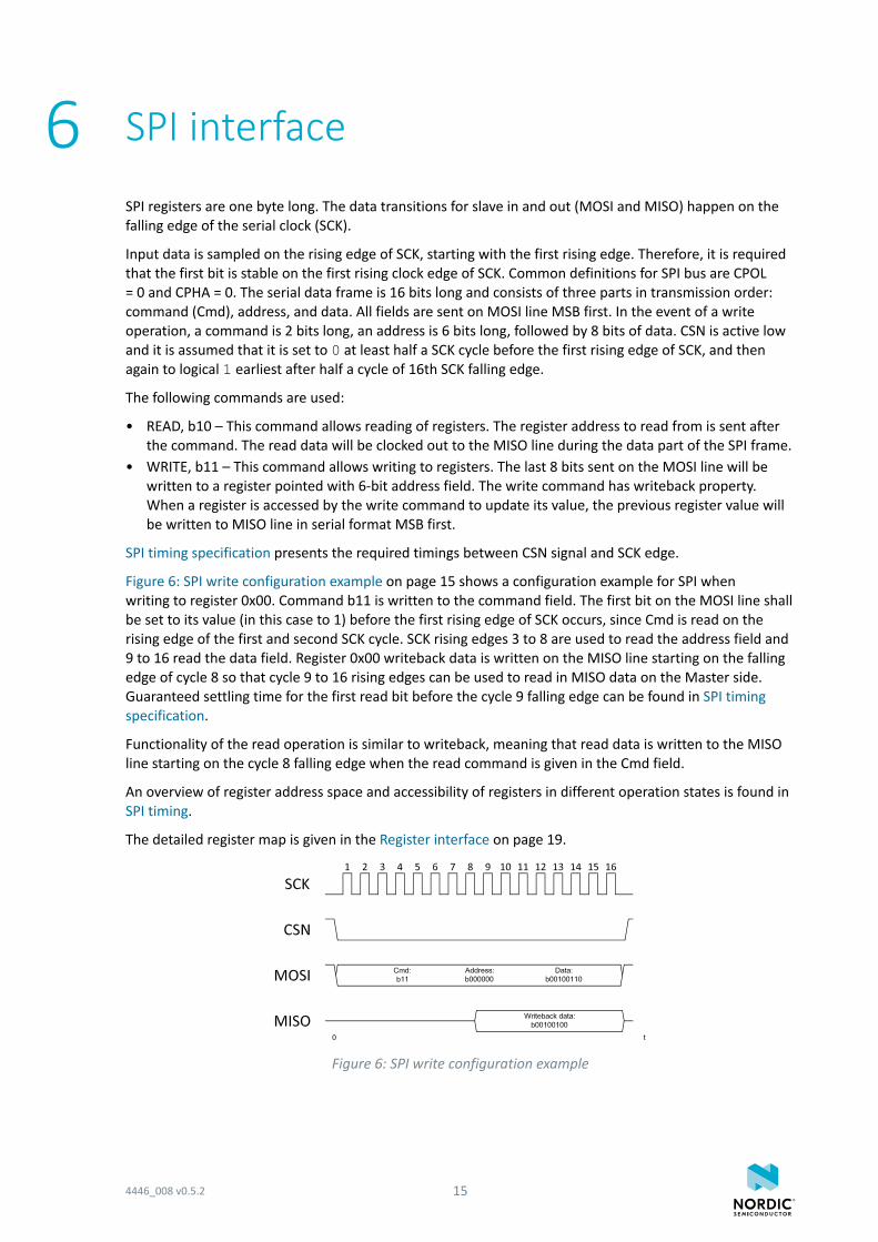
SPI registers are one byte long. The data transitions for slave in and out (MOSI and MISO) happen on thefalling edge of the serial clock (SCK).
Input data is sampled on the rising edge of SCK, starting with the first rising edge. Therefore, it is requiredthat the first bit is stable on the first rising clock edge of SCK. Common definitions for SPI bus are CPOL= 0 and CPHA = 0. The serial data frame is 16 bits long and consists of three parts in transmission order:command (Cmd), address, and data. All fields are sent on MOSI line MSB first. In the event of a writeoperation, a command is 2 bits long, an address is 6 bits long, followed by 8 bits of data. CSN is active lowand it is assumed that it is set to 0 at least half a SCK cycle before the first rising edge of SCK, and thenagain to logical 1 earliest after half a cycle of 16th SCK falling edge.
The following commands are used:
• READ, b10 – This command allows reading of registers. The register address to read from is sent afterthe command. The read data will be clocked out to the MISO line during the data part of the SPI frame.
• WRITE, b11 – This command allows writing to registers. The last 8 bits sent on the MOSI line will bewritten to a register pointed with 6-bit address field. The write command has writeback property.When a register is accessed by the write command to update its value, the previous register value willbe written to MISO line in serial format MSB first.
SPI timing specification presents the required timings between CSN signal and SCK edge.
Figure 6: SPI write configuration example on page 15 shows a configuration example for SPI whenwriting to register 0x00. Command b11 is written to the command field. The first bit on the MOSI line shallbe set to its value (in this case to 1) before the first rising edge of SCK occurs, since Cmd is read on therising edge of the first and second SCK cycle. SCK rising edges 3 to 8 are used to read the address field and9 to 16 read the data field. Register 0x00 writeback data is written on the MISO line starting on the fallingedge of cycle 8 so that cycle 9 to 16 rising edges can be used to read in MISO data on the Master side.Guaranteed settling time for the first read bit before the cycle 9 falling edge can be found in SPI timingspecification.
Functionality of the read operation is similar to writeback, meaning that read data is written to the MISOline starting on the cycle 8 falling edge when the read command is given in the Cmd field.
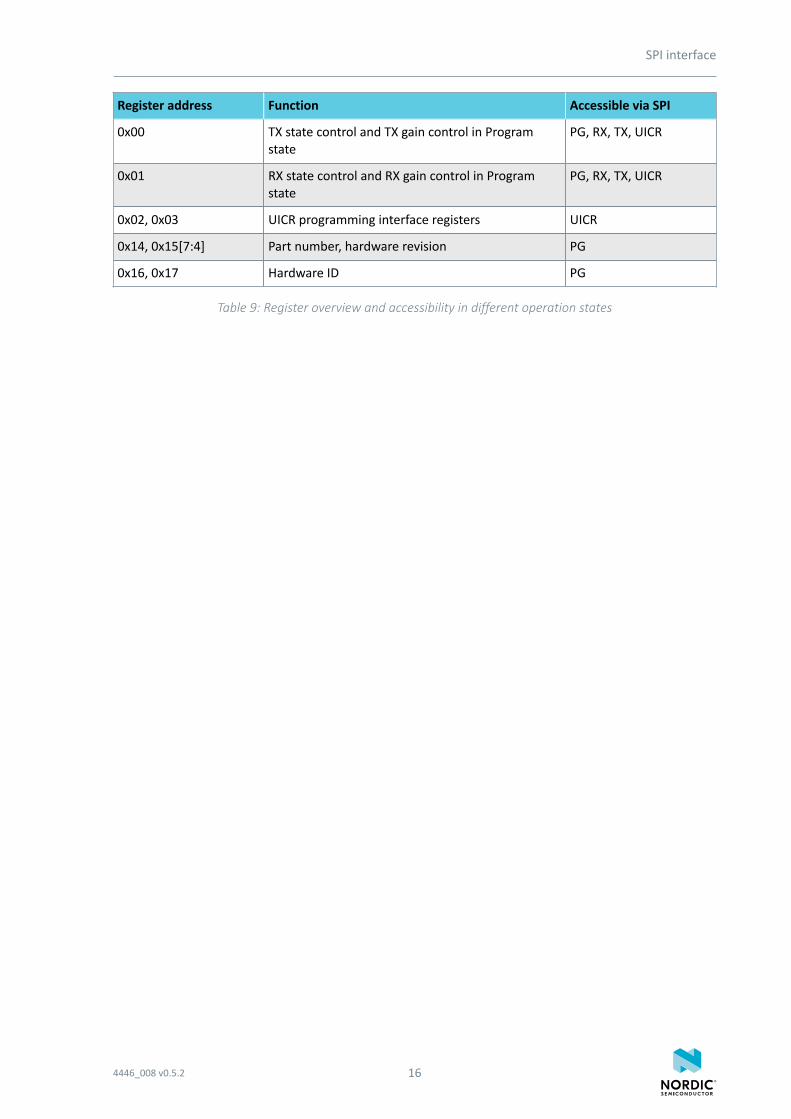
An overview of register address space and accessibility of registers in different operation states is found inSPI timing.
The detailed register map is given in the Register interface on page 19.
Figure 6: SPI write configuration example
4446_008 v0.5.2 15
SPI interface
Register address Function Accessible via SPI
0x00 TX state control and TX gain control in Programstate
PG, RX, TX, UICR
0x01 RX state control and RX gain control in Programstate
PG, RX, TX, UICR
0x02, 0x03 UICR programming interface registers UICR
0x14, 0x15[7:4] Part number, hardware revision PG
0x16, 0x17 Hardware ID PG
Table 9: Register overview and accessibility in different operation states
4446_008 v0.5.2 16
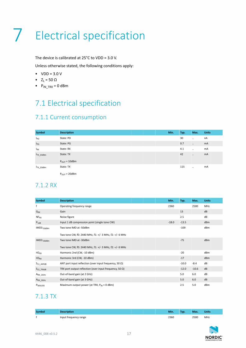
7 Electrical specification
The device is calibrated at 25°C to VDD = 3.0 V.
Unless otherwise stated, the following conditions apply:
• VDD = 3.0 V• ZL = 50 Ω• PIN_TRX = 0 dBm
7.1 Electrical specification
7.1.1 Current consumption
Symbol Description Min. Typ. Max. Units
IPD State: PD 30 .. nA
IPG State: PG 0.7 .. mA
IRX State: RX 4.1 .. mA
ITX_10dBm State: TX
POUT = 10dBm
42 .. mA
ITX_20dBm State: TX
POUT = 20dBm
115 .. mA
7.1.2 RX
Symbol Description Min. Typ. Max. Units
f Operating frequency range 2360 2500 MHz
GRX Gain 13 dB
NFRX Noise figure 2.5 dB
P1dB Input 1 dB compression point (single tone CW) -18.0 -13.5 dBm
IMD3-50dBm Two tone IMD at -50dBm
Two tone CW, f0: 2440 MHz, f1: +/- 3 MHz, f2: +/- 6 MHz
-109 dBm
IMD3-30dBm Two tone IMD at -30dBm
Two tone CW, f0: 2440 MHz, f1: +/- 3 MHz, f2: +/- 6 MHz
-75 dBm
H2RX Harmonic 2nd (CW, -10 dBm) -20 dBm
H3RX Harmonic 3rd (CW, -10 dBm) -17 dBm
S11_ANTdB ANT port input reflection (over input frequency, 50 Ω) -10.0 -8.4 dB
S22_TRXdB TRX port output reflection (over input frequency, 50 Ω) -12.0 -10.6 dB
ARX_2GHz Out-of-band gain (at 2 GHz) 5.0 6.0 dB
ARX_3GHz Out-of-band gain (at 3 GHz) 5.0 6.0 dB
PMAX,RX Maximum output power (at TRX, PIN = 0 dBm) 2.5 5.0 dBm
7.1.3 TX
Symbol Description Min. Typ. Max. Units
f Input frequency range 2360 2500 MHz
4446_008 v0.5.2 17
Electrical specification
Symbol Description Min. Typ. Max. Units
PSAT Saturated output power; GFSK/OQPSK modulation 21.5 dBm
GTX Gain (POUT<PP1dB) 20 dB
PP1dB Output power in 1dB compression; GFSK/OQPSK modulation 21 dBm
AM/AM Compression - positive 6 dB
AM/AM Compression - negative 0 dB
Tcarrier Carrier switching time
POUT from -30 dBm to +20 dBm
1 µs
PSPUR2MHz In-band spurious emissions 2 MHz (GFSK/OQPSK) -26 dBm
PSPUR3MHz In-band spurious emissions 3 MHz (GFSK/OQPSK) -36 dBm
H2, H3 Harmonic, 2nd, 3rd; RBW = 1.0 MHz -42 dBm
H4, H5 Harmonic, 4th, 5th; RBW = 1.0 MHz -36 dBm
S11_TRXdB Input reflection at TRX pin (over input frequency range, 50
Ω)
-10 -7 dB
VSWRSTB Unconditionally stable -
VSWRRGN No permanent damage (load 10:1, all phase angles) -
7.1.4 SPI timing specification
Symbol Description Min. Typ. Max. Units
TSCK SCK clock period (50% duty cycle) 125 ns
TCSN-SCK1 CSN lead time
Time from CSN set to 0 to first rising edge at SCK
62.5 ns
TSCK16-CSN CSN trail time
Time from 16th falling edge at SCK to CSN set to 1
62.5 ns
TCSN CSN idle time
Time required between consecutive transmissions
125 ns
TS_MISO MISO settling time
Guaranteed settling margin for MISO before 9th rising edge
at SCK
30 ns
4446_008 v0.5.2 18
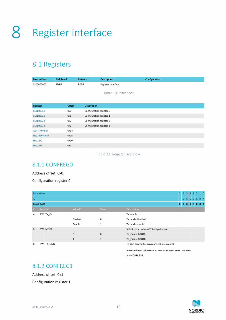
8 Register interface
8.1 Registers
Base address Peripheral Instance Description Configuration
0x00000000 REGIF REGIF Register interface
Table 10: Instances
Register Offset Description
CONFREG0 0x0 Configuration register 0
CONFREG1 0x1 Configuration register 1
CONFREG2 0x2 Configuration register 2
CONFREG3 0x3 Configuration register 3
PARTNUMBER 0x14
HW_REVISION 0x15
HW_ID0 0x16
HW_ID1 0x17
Table 11: Register overview
8.1.1 CONFREG0Address offset: 0x0
Configuration register 0
Bit number 7 6 5 4 3 2 1 0
ID C C C C C B A
Reset 0x00 0 0 0 0 0 0 0 0
ID AccessField Value ID Value Description
A RW TX_EN TX enable
Disable 0 TX mode disabled
Enable 1 TX mode enabled
B RW MODE Select preset value of TX output power.
0 0 TX_Gain = POUTA
1 1 TX_Gain = POUTB
C RW TX_GAIN TX gain control (0: minimum, 31: maximum)
Initialized with value from POUTA or POUTB. See CONFREG2
and CONFREG3.
8.1.2 CONFREG1Address offset: 0x1
Configuration register 1
4446_008 v0.5.2 19
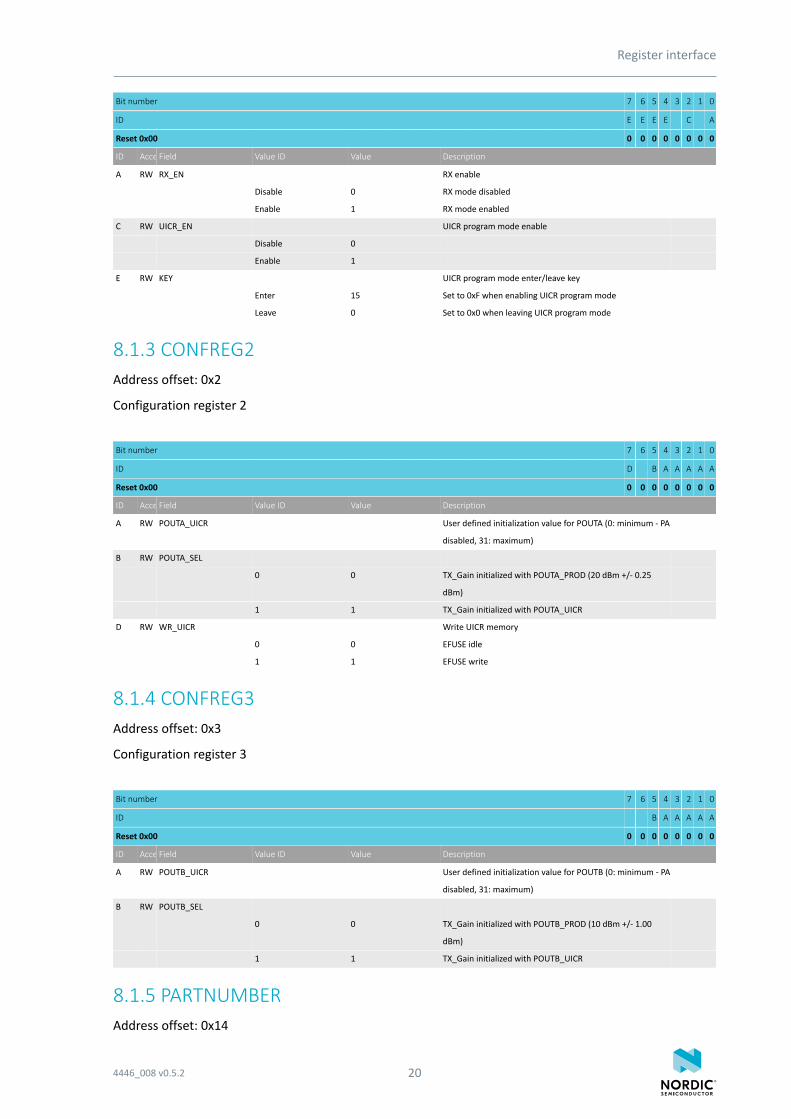
Register interface
Bit number 7 6 5 4 3 2 1 0
ID E E E E C A
Reset 0x00 0 0 0 0 0 0 0 0
ID AccessField Value ID Value Description
A RW RX_EN RX enable
Disable 0 RX mode disabled
Enable 1 RX mode enabled
C RW UICR_EN UICR program mode enable
Disable 0
Enable 1
E RW KEY UICR program mode enter/leave key
Enter 15 Set to 0xF when enabling UICR program mode
Leave 0 Set to 0x0 when leaving UICR program mode
8.1.3 CONFREG2Address offset: 0x2
Configuration register 2
Bit number 7 6 5 4 3 2 1 0
ID D B A A A A A
Reset 0x00 0 0 0 0 0 0 0 0
ID AccessField Value ID Value Description
A RW POUTA_UICR User defined initialization value for POUTA (0: minimum - PA
disabled, 31: maximum)
B RW POUTA_SEL
0 0 TX_Gain initialized with POUTA_PROD (20 dBm +/- 0.25
dBm)
1 1 TX_Gain initialized with POUTA_UICR
D RW WR_UICR Write UICR memory
0 0 EFUSE idle
1 1 EFUSE write
8.1.4 CONFREG3Address offset: 0x3
Configuration register 3
Bit number 7 6 5 4 3 2 1 0
ID B A A A A A
Reset 0x00 0 0 0 0 0 0 0 0
ID AccessField Value ID Value Description
A RW POUTB_UICR User defined initialization value for POUTB (0: minimum - PA
disabled, 31: maximum)
B RW POUTB_SEL
0 0 TX_Gain initialized with POUTB_PROD (10 dBm +/- 1.00
dBm)
1 1 TX_Gain initialized with POUTB_UICR
8.1.5 PARTNUMBERAddress offset: 0x14
4446_008 v0.5.2 20
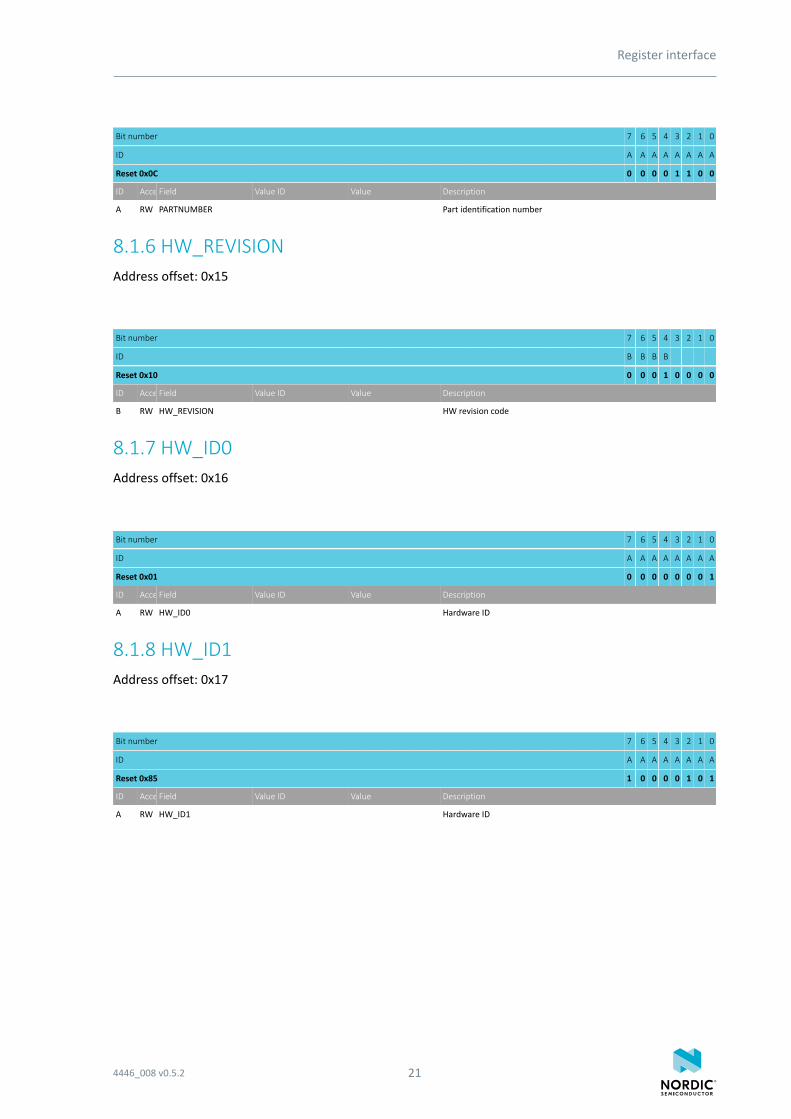
Register interface
Bit number 7 6 5 4 3 2 1 0
ID A A A A A A A A
Reset 0x0C 0 0 0 0 1 1 0 0
ID AccessField Value ID Value Description
A RW PARTNUMBER Part identification number
8.1.6 HW_REVISIONAddress offset: 0x15
Bit number 7 6 5 4 3 2 1 0
ID B B B B
Reset 0x10 0 0 0 1 0 0 0 0
ID AccessField Value ID Value Description
B RW HW_REVISION HW revision code
8.1.7 HW_ID0Address offset: 0x16
Bit number 7 6 5 4 3 2 1 0
ID A A A A A A A A
Reset 0x01 0 0 0 0 0 0 0 1
ID AccessField Value ID Value Description
A RW HW_ID0 Hardware ID
8.1.8 HW_ID1Address offset: 0x17
Bit number 7 6 5 4 3 2 1 0
ID A A A A A A A A
Reset 0x85 1 0 0 0 0 1 0 1
ID AccessField Value ID Value Description
A RW HW_ID1 Hardware ID
4446_008 v0.5.2 21
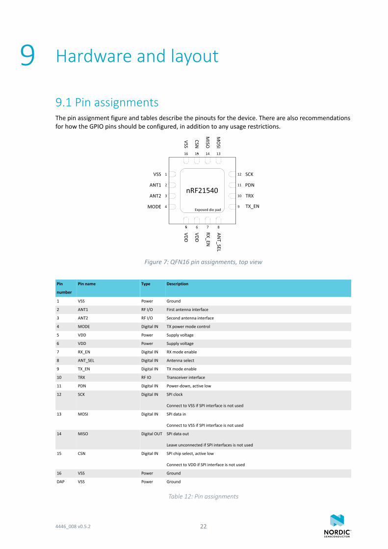
9 Hardware and layout
9.1 Pin assignmentsThe pin assignment figure and tables describe the pinouts for the device. There are also recommendationsfor how the GPIO pins should be configured, in addition to any usage restrictions.
Figure 7: QFN16 pin assignments, top view
Pin
number
Pin name Type Description
1 VSS Power Ground
2 ANT1 RF I/O First antenna interface
3 ANT2 RF I/O Second antenna interface
4 MODE Digital IN TX power mode control
5 VDD Power Supply voltage
6 VDD Power Supply voltage
7 RX_EN Digital IN RX mode enable
8 ANT_SEL Digital IN Antenna select
9 TX_EN Digital IN TX mode enable
10 TRX RF IO Transceiver interface
11 PDN Digital IN Power-down, active low
12 SCK Digital IN SPI clock
Connect to VSS if SPI interface is not used
13 MOSI Digital IN SPI data in
Connect to VSS if SPI interface is not used
14 MISO Digital OUT SPI data out
Leave unconnected if SPI interfaces is not used
15 CSN Digital IN SPI chip select, active low
Connect to VDD if SPI interface is not used
16 VSS Power Ground
DAP VSS Power Ground
Table 12: Pin assignments
4446_008 v0.5.2 22
Hardware and layout
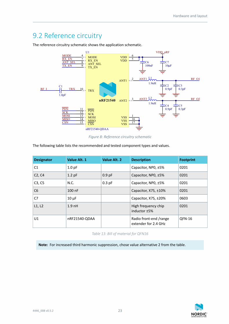
9.2 Reference circuitryThe reference circuitry schematic shows the application schematic.
Figure 8: Reference circuitry schematic
The following table lists the recommended and tested component types and values.
Designator Value Alt. 1 Value Alt. 2 Description Footprint
C1 1.0 pF Capacitor, NP0, ±5% 0201
C2, C4 1.2 pF 0.9 pF Capacitor, NP0, ±5% 0201
C3, C5 N.C. 0.3 pF Capacitor, NP0, ±5% 0201
C6 100 nF Capacitor, X7S, ±10% 0201
C7 10 µF Capacitor, X7S, ±20% 0603
L1, L2 1.9 nH High frequency chipinductor ±5%
0201
U1 nRF21540-QDAA Radio front-end /rangeextender for 2.4 GHz
QFN-16
Table 13: Bill of material for QFN16
Note: For increased third harmonic suppression, chose value alternative 2 from the table.
4446_008 v0.5.2 23
10 Recommended operating conditions
The operating conditions are the physical parameters that the chip can operate within.
Symbol Parameter Notes Min. Nom. Max. Units
VDD Main supply voltage/battery Functional range 1.7 3.0 3.6 V
VIH Digital input high SPI, PDN, ANT_SEL 0.7 VVDD VVDD V
VIL Digital input low SPI, PDN, ANT_SEL VVSS 0.3 VVDD V
FSCK SPI clock frequency Exceeding may cause SPI malfunction 8 MHz
CMISO MISO load capacitance Exceeding may cause SPI read malfunction 50 pF
TOP Operating temperature range Board temperature, 1 mm from the package -40 +25 +105 °C
ZL Load impedance 50 Ω
Table 14: Recommended operating conditions
4446_008 v0.5.2 24
11 Absolute maximum ratings
Maximum ratings are the extreme limits to which the chip can be exposed to for a limited amount of timewithout permanently damaging it. Exposure to absolute maximum ratings for prolonged periods of timemay affect the reliability of the device.
Note Min. Max. Unit
Supply voltage
VDD 0 3.6 V
VSS 0 V
Digital I/O pin voltage
VI/O VDD ≤ 3.6 V -0.3 VDD + 0.3 V
RF I/O pin voltage
VANT TBD TBD V
VTRX TBD TBD V
RF I/O pin input power
PIN_TRX CW, Transmit mode +5 dBm
PIN_ANT CW, Receive/Program mode +15 dBm
Environmental
Storage temperature -40 125 °C
Reflow soldering temperature IPC/JEDEC J-STD-020 260 °C
MSL Moisture sensitivity level
ESD HBM Human Body Model 2 kV
ESD CDM Charged Device Model 1 kV
Table 15: Absolute maximum ratings
4446_008 v0.5.2 25

12 Legal notices
By using this documentation you agree to our terms and conditions of use. Nordic Semiconductor maychange these terms and conditions at any time without notice.
Liability disclaimerNordic Semiconductor ASA reserves the right to make changes without further notice to the product toimprove reliability, function, or design. Nordic Semiconductor ASA does not assume any liability arising outof the application or use of any product or circuits described herein.
Nordic Semiconductor ASA does not give any representations or warranties, expressed or implied, as tothe accuracy or completeness of such information and shall have no liability for the consequences of useof such information. If there are any discrepancies, ambiguities or conflicts in Nordic Semiconductor’sdocumentation, the Product Specification prevails.
Nordic Semiconductor ASA reserves the right to make corrections, enhancements, and other changes tothis document without notice.
Life support applicationsNordic Semiconductor products are not designed for use in life support appliances, devices, or systemswhere malfunction of these products can reasonably be expected to result in personal injury.
Nordic Semiconductor ASA customers using or selling these products for use in such applications do soat their own risk and agree to fully indemnify Nordic Semiconductor ASA for any damages resulting fromsuch improper use or sale.
RoHS and REACH statementRefer to www.nordicsemi.com for complete hazardous substance reports, material composition reports,and latest version of Nordic’s RoHS and REACH statements.
TrademarksAll trademarks, service marks, trade names, product names, and logos appearing in this documentationare the property of their respective owners.
Copyright notice© 2019 Nordic Semiconductor ASA. All rights are reserved. Reproduction in whole or in part is prohibitedwithout the prior written permission of the copyright holder.
4446_008 v0.5.2 26