np-dynamic skybridge: a fine-grained 3d ic … skybridge: a fine-grained 3d ic technology with...
TRANSCRIPT
NP-Dynamic Skybridge: A Fine-Grained 3D ICTechnology with NP-Dynamic Logic
JIAJUN SHI, MINGYU LI, MOSTAFIZUR RAHMAN, SANTOSH KHASANVIS, AND CSABA ANDRAS MORITZJ. Shi, M. Li, and C.A. Moritz are with the Department of Electrical and Computer Engineering, University of Massachusetts, Amherst, MA 01003
M. Rahman is with the School of Computing and Engineering, University of Missouri, Kansas City, MO 65211S. Khasanvis is with BlueRISC Inc., Amherst, MA 01002
CORRESPONDING AUTHOR: J. SHI ([email protected])
ABSTRACT A new 3D IC fabric named NP-Dynamic Skybridge is proposed that provides fine-grainedvertical 3D integration for future technology scaling. Relying on a template of vertical nanowires, it expandsour prior work to incorporate and utilize both n- and p-type transistors in a novel NP-Dynamic circuit-stylecompatible with true 3D integration. This enables a wide range of elementary logics leading to more compactcircuits, simple clocking schemes for cascading logic stages and low buffer requirement. We detail newdesign concepts for larger-scale circuits, and evaluate our approach using a 4-bit nanoprocessor implementedin 16 nm technology node. A new pipelining scheme specifically designed for our 3D NP-Dynamic circuitsis employed in the nanoprocessor. We compare our approach with 2D CMOS as well as state-of-the-art tran-sistor-level monolithic 3D IC (T-MI) approach. Benchmarking results for the 4-bit nanoprocessor show bene-fits of up to 56.7x density, 3.8x power and 1.7x throughput over 2D CMOS. Compared with T-MI, our new3D fabric showed 31x density, 3x power and 1.4x throughput improvement. Additional evaluation of 4-bitand 8-bit CLA designs shows that significantly improved gains can be achieved for our 3D approach over 2DCMOS with increasing circuit bit-width, indicating potential for future scalability.
INDEX TERMS 3D IC fabric, NP-Dynamic circuits, emerging technologies, vertical nanowires, nanoscalecomputing fabrics, nanoprocessor
I. INTRODUCTION
2D CMOS integrated circuit (IC) technology scaling facessevere challenges that result from device scaling limitations[1], [2], interconnect bottleneck that dominates power andperformance [3], etc. 3D ICs with die-die and layer-layerstacking using Through Silicon Vias (TSVs) [4] and Mono-lithic Inter-layer Vias (MIVs) [5] have been explored in recentyears to generate circuits with considerable interconnect sav-ing for continuing technology scaling. However, these 3D ICtechnologies still rely on conventional 2D CMOS’s device,circuit and interconnect mindset showing only incrementalbenefits [8] while adding new challenges such as thermalmanagement, manufacturing and reliability issues [4], [5].In [6], [7], a vertical nanowire based 3D integrated circuit
fabric called Skybridge was proposed showing a pathway fortruly fine-grained 3D integration. In this 3D fabric, core ICfabric aspects from device to circuit-style, connectivity [9],thermal management [10] and manufacturing pathway [11]are co-architected keeping 3D compatibility in mind, and usesthe vertical dimension instead of a multi-layered 2D mindset.
In the Skybridge fabric, uniform n-type transistors are used ina dynamic circuit style [6], and n-type transistor based NANDand AND-of-NAND compound gates are the elementary logicfunctions. Multiple clock signals are used to control the cas-cading of elementary logic stages, and buffers are used in-between stages for signal propagation and restoration in large-scale designs, which introduce limitations.Here, we propose NP-Dynamic Skybridge fabric [12] that
incorporates both n- and p-type transistors to build a newclass of fine-grained 3D integrated circuits. It follows a fab-ric-centric mindset to integrate both n- and p-type circuitcomponents in the physical layer for 3D compatibility. Theuse of both n- and p-type transistors allows a wide range ofelementary logic functions to be supported including NAND,AND-of-NAND, NOR and OR-of-NOR, which provide highflexibility for implementation of logic functions. This resultsin compact circuit designs with short interconnects and lowbuffer requirement. The use of NP-Dynamic circuit style alsoallows a simple clocking scheme (since alternately cascadingn- and p-type logic stages maps intrinsically to the signal
Received 13 June 2016; revised 24 February 2017; accepted 8 March 2017.Date of publication 20 March 2017; date of current version 7 June 2017.
Digital Object Identifier 10.1109/TETC.2017.2684781
286
2168-6750� 2017 IEEE. Translations and content mining are permitted for academic research only.
Personal use is also permitted, but republication/redistribution requires IEEE permission.
See http://www.ieee.org/publications_standards/publications/rights/index.html for more information. VOLUME 5, NO. 2, APRIL-JUNE 2017
monotonicity requirement of dynamic circuits). The achieveddesign with unique 3D components has good connectivity [9]and routability [13] to address high-density interconnects inlarger-scale circuits, which leads to compact circuit designwith significant power efficiency and high performance.In this paper, the NP-Dynamic Skybridge approach is
extensively evaluated at the circuit-level and system-level toinvestigate its benefits in circuit designs with complex andhigh-density interconnects. For circuit-level evaluation, itscore fabric components including fabric structures facilitat-ing both n- and p-type integration and elementary logic gatescombined with TCAD and HSPICE simulations are pre-sented in detail. For system-level evaluation, a 4-bit WireStream Processor (WISP-4) [14] design is used as bench-mark. A new pipelining scheme specifically designed forNP-Dynamic 3D circuit style is used in the WISP-4 design toreduce the operation time of each stage in pipeline forimproved throughput. Device-to-circuit fabric evaluation ispresented for WISP-4 accounting for characteristics ofselected materials, circuit style, placement and routing, and3D layouts, which shows up to 56.7x density benefit, 3.8xpower efficiency and 1.7x benefit in throughput against 2DCMOS with the equivalent technology node. We also com-pare our approach with the state-of-the-art approach of con-ventional 3D IC direction, the transistor-level monolithic 3DIC (T-MI) [15] using equivalent technology node. Our 3Dapproach showed up to 31x density benefit, 3x power effi-ciency and 1.4x benefit in throughput against T-MI 3D IC.Additionally, we used 4-bit and 8-bit CLAs as benchmark toevaluate NP-Dynamic Skybridge’s gain over 2D CMOS asthe bit-width of design grows; NP-Dynamic’s 8-bit CLAdesign has 24 percent increased latency and 16 percentincreased power compared with 4-bit CLA design while 2DCMOS’s 8-bit CLA design has 2x latency and 25 percentincreased power compared with 4-bit CLA design.The rest of the paper is organized as follows: Section II
presents the proposed 3D fabric’s core components. In SectionIII, we show the elementary gates and their fan-in sensitivityanalysis. Section IV shows a device-to-circuit evaluationmethodology for this new fabric. Then, in Section V, we showthe benchmarking of a 4-bit nanoprocessor (WISP-4) with anoptimized pipelining scheme for improved throughput versus2D CMOS and T-MI 3D. Section VI presents a preliminarystudy of gain versus bit-width utilizing carry look-ahead adderdesigns. Section VII concludes the paper.
II. ENABLING 3D INTEGRATION: CORE COMPONENTS
NP-Dynamic Skybridge follows a fabric-centric mindset tocreate a truly fine-grained 3D integration system in the verti-cal dimension. Each core component is designed for 3D com-patibility and overall system efficiency. These componentsare assembled on a 3D uniform template of single crystalnanowires that act as scaffolding for vertical assembly.While extensive device-to-circuit aspects and evaluation are
shown in this work, as well as experimental progress of keyprocess steps involved, its full experimental demonstration
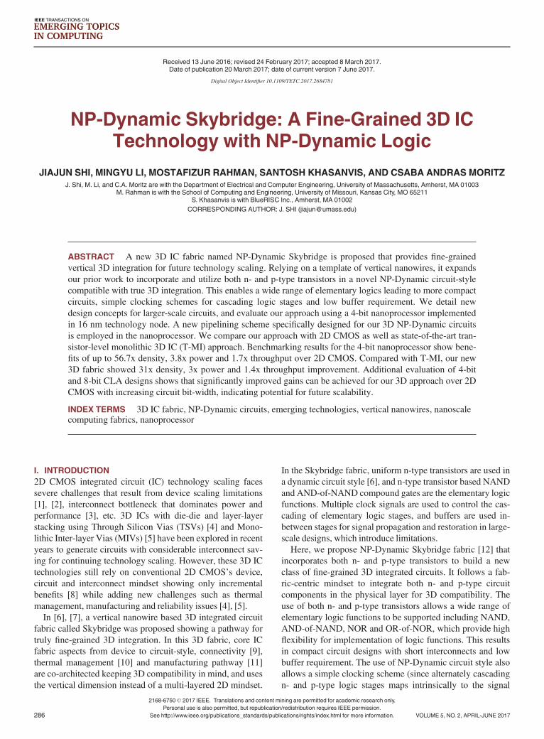
towards a functional circuit is an ongoing long-term effort.Figure 1A shows the envisioned NP-Dynamic Skybridge;Using a similar process flow described in [11], vertical nano-wires, are constructed primarily through masking and highaspect ratio etching on heavily doped silicon bulk (other meth-ods are also possible). Architected fabric components are con-structed on these nanowires by using material depositiontechniques [11]. In this section, we present the core compo-nents that enable fine-grained integration of both n- and p-typenanowires in Skybridge fabric. Detailed explanation of mate-rial selection and working mechanism are presented to illus-trate how these components are used in unison to achievedesired functionality and 3D compatibility with circuits imple-mented across both horizontal and vertical dimensions.
A. VERTICAL NANOWIRES
Vertical nanowires are the fundamental building blocks thatenable vertical stacking of designed core Skybridge compo-nents. The nanowires serve multiple functions – they can actas (i) logic nanowires that have stacked transistors to imple-ment required logic gates, (ii) routing nanowires to carryelectrical signals along the vertical dimension, and (iii) heatdissipating nanowires to extract and sink heat generated dur-ing circuit operation to the bulk substrate [10].The nanowire formation step precedes all manufacturing
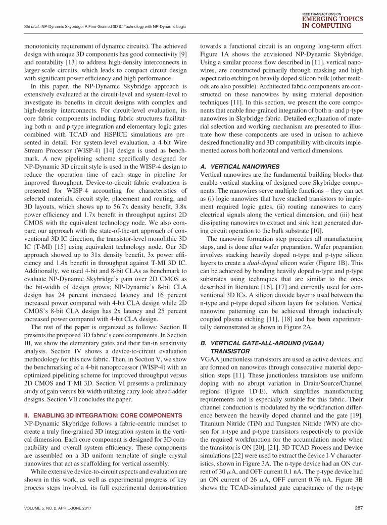
steps, and is done after wafer preparation. Wafer preparationinvolves stacking heavily doped n-type and p-type siliconlayers to create a dual-doped silicon wafer (Figure 1B). Thiscan be achieved by bonding heavily doped n-type and p-typesubstrates using techniques that are similar to the onesdescribed in literature [16], [17] and currently used for con-ventional 3D ICs. A silicon dioxide layer is used between then-type and p-type doped silicon layers for isolation. Verticalnanowire patterning can be achieved through inductivelycoupled plasma etching [11], [18] and has been experimen-tally demonstrated as shown in Figure 2A.
B. VERTICAL GATE-ALL-AROUND (VGAA)
TRANSISTOR
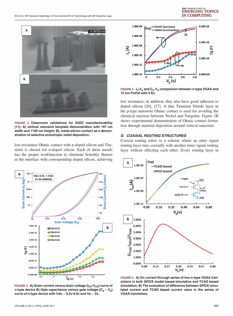
VGAA junctionless transistors are used as active devices, andare formed on nanowires through consecutive material depo-sition steps [11]. These junctionless transistors use uniformdoping with no abrupt variation in Drain/Source/Channelregions (Figure 1D-E), which simplifies manufacturingrequirements and is especially suitable for this fabric. Theirchannel conduction is modulated by the workfunction differ-ence between the heavily doped channel and the gate [19].Titanium Nitride (TiN) and Tungsten Nitride (WN) are cho-sen for n-type and p-type transistors respectively to providethe required workfunction for the accumulation mode whenthe transistor is ON [20], [21]. 3D TCAD Process and Devicesimulations [22] were used to extract the device I-V character-istics, shown in Figure 3A. The n-type device had an ON cur-rent of 30mA, and OFF current 0.1 nA. The p-type device hadan ON current of 26 mA, OFF current 0.76 nA. Figure 3Bshows the TCAD-simulated gate capacitance of the n-type
VOLUME 5, NO. 2, APRIL-JUNE 2017 287
Shi et al.: NP-Dynamic Skybridge: A Fine-Grained 3D IC Technology with NP-Dynamic Logic
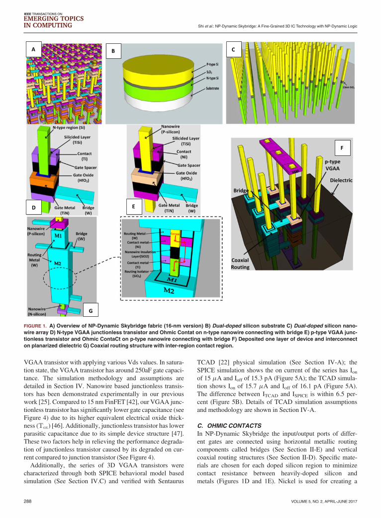
VGAA transistor with applying various Vds values. In satura-tion state, the VGAA transistor has around 250aF gate capaci-tance. The simulation methodology and assumptions aredetailed in Section IV. Nanowire based junctionless transis-tors has been demonstrated experimentally in our previouswork [25]. Compared to 15 nm FinFET [42], our VGAA junc-tionless transistor has significantly lower gate capacitance (seeFigure 4) due to its higher equivalent electrical oxide thick-ness (Tox) [46]. Additionally, junctionless transistor has lowerparasitic capacitance due to its simple device structure [47].These two factors help in relieving the performance degrada-tion of junctionless transistor caused by its degraded on cur-rent compared to junction transistor (See Figure 4).Additionally, the series of 3D VGAA transistors were
characterized through both SPICE behavioral model basedsimulation (See Section IV.C) and verified with Sentaurus
TCAD [22] physical simulation (See Section IV-A); theSPICE simulation shows the on current of the series has Ionof 15 mA and Ioff of 15.3 pA (Figure 5A); the TCAD simula-tion shows Ion of 15.7 mA and Ioff of 16.1 pA (Figure 5A).The difference between ITCAD and ISPICE is within 6.5 per-cent (Figure 5B). Details of TCAD simulation assumptionsand methodology are shown in Section IV-A.
C. OHMIC CONTACTS
In NP-Dynamic Skybridge the input/output ports of differ-ent gates are connected using horizontal metallic routingcomponents called bridges (See Section II-E) and verticalcoaxial routing structures (See Section II-D). Specific mate-rials are chosen for each doped silicon region to minimizecontact resistance between heavily-doped silicon andmetals (Figures 1D and 1E). Nickel is used for creating a
FIGURE 1. A) Overview of NP-Dynamic Skybridge fabric (16-nm version) B) Dual-doped silicon substrate C) Dual-doped silicon nano-
wire array D) N-type VGAA junctionless transistor and Ohmic Contat on n-type nanowire connecting with bridge E) p-type VGAA junc-
tionless transistor and Ohmic ContaCt on p-type nanowire connecting with bridge F) Deposited one layer of device and interconnect
on planarized dielectric G) Coaxial routing structure with inter-region contact region.
288 VOLUME 5, NO. 2, APRIL-JUNE 2017
Shi et al.: NP-Dynamic Skybridge: A Fine-Grained 3D IC Technology with NP-Dynamic Logic
low-resistance Ohmic contact with p-doped silicon and Tita-nium is chosen for n-doped silicon. Each of these metalshas the proper workfunction to eliminate Schottky Barrierin the interface with corresponding doped silicon, achieving
low resistance; in addition, they also have good adhesion todoped silicon [26], [27]. A thin Titanium Nitride layer inthe p-type nanowire Ohmic contact is used for avoiding thechemical reaction between Nickel and Tungsten. Figure 2Bshows experimental demonstration of Ohmic contact forma-tion through material deposition around vertical nanowire.
D. COAXIAL ROUTING STRUCTURES
Coaxial routing refers to a scheme where an outer signalrouting layer runs coaxially with another inner signal routinglayer without affecting each other. Every routing layer in
FIGURE 3. A) Drain current versus drain voltage (IDS-VDS) curve of
n-type device B) Gate capacitance versus gate voltage (Cg – Vg)
curve of n-type device with Vds ¼ 0.2v-0.8v and Vs ¼ 0v.
FIGURE 4. Id-Vg and Cg-Vg comparison between n-type VGAA and
15 nm FinFet with 4 fin.
FIGURE 2. Cleanroom validations for S3DC manufacturability
[11]: A) vertical nanowire template demonstration with 197 nm
width and 1100 nm height; B). metal-silicon contact as a demon-
stration of selective anisotropic metal deposition.
FIGURE 5. A) On current through series of two n-type VGAA tran-
sistors in both SPICE model based simulation and TCAD based
simulation; B) The evaluation of difference between SPICE simu-
lated current and TCAD based current value in the series of
VGAA transistors.
VOLUME 5, NO. 2, APRIL-JUNE 2017 289
Shi et al.: NP-Dynamic Skybridge: A Fine-Grained 3D IC Technology with NP-Dynamic Logic
such a coaxial structure facilitates signal propagation alongthe vertical dimension. This is unique and enabled by the fab-ric’s vertical integration approach, and can be manufacturedsimilar to the process flow used in [11]. A coaxial routingstructure (Figure 1G) consists of two concentric metal layersseparated by dielectric layers around a nanowire. The outer-most metal shell (M2) and the inner nanowire are used forcarrying input/output signals. Electrical coupling noisebetween the inner nanowire and outer metal shell can be miti-gated by pinning the inner metal shell (M1) to a ground(GND) signal for shielding. Figure 1G illustrates this con-cept; the GND signal is applied to the M1 metal shell whichthus acts as a shield layer, and prevents coupling betweensignals in M2 shell and the inner nanowire.Given that a nanowire itself can carry a signal and the
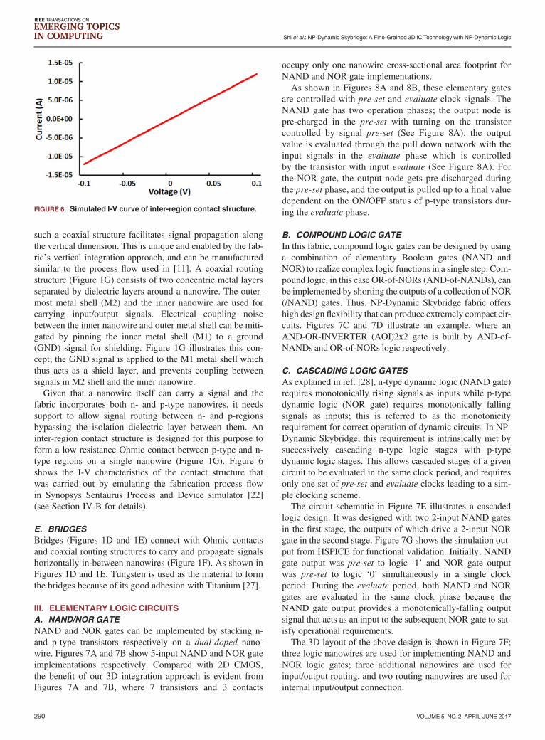
fabric incorporates both n- and p-type nanowires, it needssupport to allow signal routing between n- and p-regionsbypassing the isolation dielectric layer between them. Aninter-region contact structure is designed for this purpose toform a low resistance Ohmic contact between p-type and n-type regions on a single nanowire (Figure 1G). Figure 6shows the I-V characteristics of the contact structure thatwas carried out by emulating the fabrication process flowin Synopsys Sentaurus Process and Device simulator [22](see Section IV-B for details).
E. BRIDGES
Bridges (Figures 1D and 1E) connect with Ohmic contactsand coaxial routing structures to carry and propagate signalshorizontally in-between nanowires (Figure 1F). As shown inFigures 1D and 1E, Tungsten is used as the material to formthe bridges because of its good adhesion with Titanium [27].
III. ELEMENTARY LOGIC CIRCUITS
A. NAND/NOR GATE
NAND and NOR gates can be implemented by stacking n-and p-type transistors respectively on a dual-doped nano-wire. Figures 7A and 7B show 5-input NAND and NOR gateimplementations respectively. Compared with 2D CMOS,the benefit of our 3D integration approach is evident fromFigures 7A and 7B, where 7 transistors and 3 contacts
occupy only one nanowire cross-sectional area footprint forNAND and NOR gate implementations.As shown in Figures 8A and 8B, these elementary gates
are controlled with pre-set and evaluate clock signals. TheNAND gate has two operation phases; the output node ispre-charged in the pre-set with turning on the transistorcontrolled by signal pre-set (See Figure 8A); the outputvalue is evaluated through the pull down network with theinput signals in the evaluate phase which is controlledby the transistor with input evaluate (See Figure 8A). Forthe NOR gate, the output node gets pre-discharged duringthe pre-set phase, and the output is pulled up to a final valuedependent on the ON/OFF status of p-type transistors dur-ing the evaluate phase.
B. COMPOUND LOGIC GATE
In this fabric, compound logic gates can be designed by usinga combination of elementary Boolean gates (NAND andNOR) to realize complex logic functions in a single step. Com-pound logic, in this case OR-of-NORs (AND-of-NANDs), canbe implemented by shorting the outputs of a collection of NOR(/NAND) gates. Thus, NP-Dynamic Skybridge fabric offershigh design flexibility that can produce extremely compact cir-cuits. Figures 7C and 7D illustrate an example, where anAND-OR-INVERTER (AOI)2x2 gate is built by AND-of-NANDs and OR-of-NORs logic respectively.
C. CASCADING LOGIC GATES
As explained in ref. [28], n-type dynamic logic (NAND gate)requires monotonically rising signals as inputs while p-typedynamic logic (NOR gate) requires monotonically fallingsignals as inputs; this is referred to as the monotonicityrequirement for correct operation of dynamic circuits. In NP-Dynamic Skybridge, this requirement is intrinsically met bysuccessively cascading n-type logic stages with p-typedynamic logic stages. This allows cascaded stages of a givencircuit to be evaluated in the same clock period, and requiresonly one set of pre-set and evaluate clocks leading to a sim-ple clocking scheme.The circuit schematic in Figure 7E illustrates a cascaded
logic design. It was designed with two 2-input NAND gatesin the first stage, the outputs of which drive a 2-input NORgate in the second stage. Figure 7G shows the simulation out-put from HSPICE for functional validation. Initially, NANDgate output was pre-set to logic ‘1’ and NOR gate outputwas pre-set to logic ‘0’ simultaneously in a single clockperiod. During the evaluate period, both NAND and NORgates are evaluated in the same clock phase because theNAND gate output provides a monotonically-falling outputsignal that acts as an input to the subsequent NOR gate to sat-isfy operational requirements.The 3D layout of the above design is shown in Figure 7F;
three logic nanowires are used for implementing NAND andNOR logic gates; three additional nanowires are used forinput/output routing, and two routing nanowires are used forinternal input/output connection.
FIGURE 6. Simulated I-V curve of inter-region contact structure.
290 VOLUME 5, NO. 2, APRIL-JUNE 2017
Shi et al.: NP-Dynamic Skybridge: A Fine-Grained 3D IC Technology with NP-Dynamic Logic
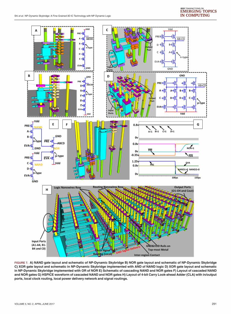
FIGURE 7. A) NAND gate layout and schematic of NP-Dynamic Skybridge B) NOR gate layout and schematic of NP-Dynamic Skybridge
C) XOR gate layout and schematic in NP-Dynamic Skybridge implemented with AND of NAND logic D) XOR gate layout and schematic
in NP-Dynamic Skybridge implemented with OR of NOR E) Schematic of cascading NAND and NOR gates F) Layout of cascaded NAND
and NOR gates G) HSPICE waveform of cascaded NAND and NOR gates H) Layout of 4-bit Carry Look-ahead Adder (CLA) with in/output
ports, local clock routing, local power delivery network and signal routings.
VOLUME 5, NO. 2, APRIL-JUNE 2017 291
Shi et al.: NP-Dynamic Skybridge: A Fine-Grained 3D IC Technology with NP-Dynamic Logic
D. FAN-IN CONSIDERATIONS
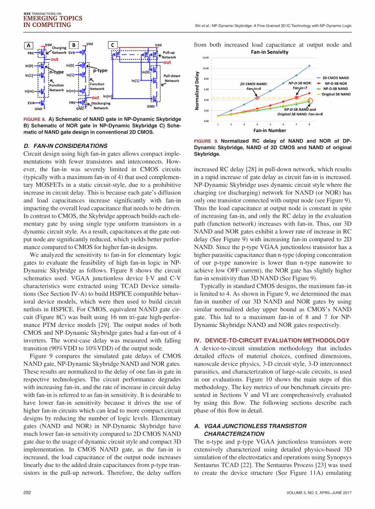
Circuit design using high fan-in gates allows compact imple-mentations with fewer transistors and interconnects. How-ever, the fan-in was severely limited in CMOS circuits(typically with a maximum fan-in of 4) that used complemen-tary MOSFETs in a static circuit-style, due to a prohibitiveincrease in circuit delay. This is because each gate’s diffusionand load capacitances increase significantly with fan-inimpacting the overall load capacitance that needs to be driven.In contrast to CMOS, the Skybridge approach builds each ele-mentary gate by using single type uniform transistors in adynamic circuit style. As a result, capacitances at the gate out-put node are significantly reduced, which yields better perfor-mance compared to CMOS for higher fan-in designs.We analyzed the sensitivity to fan-in for elementary logic
gates to evaluate the feasibility of high fan-in logic in NP-Dynamic Skybridge as follows. Figure 8 shows the circuitschematics used. VGAA junctionless device I-V and C-Vcharacteristics were extracted using TCAD Device simula-tions (See Section IV-A) to build HSPICE compatible behav-ioral device models, which were then used to build circuitnetlists in HSPICE. For CMOS, equivalent NAND gate cir-cuit (Figure 8C) was built using 16 nm tri-gate high-perfor-mance PTM device models [29]. The output nodes of bothCMOS and NP-Dynamic Skybridge gates had a fan-out of 4inverters. The worst-case delay was measured with fallingtransition (90%VDD to 10%VDD) of the output node.Figure 9 compares the simulated gate delays of CMOS
NAND gate, NP-Dynamic Skybridge NAND and NOR gates.These results are normalized to the delay of one fan-in gate inrespective technologies. The circuit performance degradeswith increasing fan-in, and the rate of increase in circuit delaywith fan-in is referred to as fan-in sensitivity. It is desirable tohave lower fan-in sensitivity because it drives the use ofhigher fan-in circuits which can lead to more compact circuitdesigns by reducing the number of logic levels. Elementarygates (NAND and NOR) in NP-Dynamic Skybridge havemuch lower fan-in sensitivity compared to 2D CMOS NANDgate due to the usage of dynamic circuit style and compact 3Dimplementation. In CMOS NAND gate, as the fan-in isincreased, the load capacitance of the output node increaseslinearly due to the added drain capacitances from p-type tran-sistors in the pull-up network. Therefore, the delay suffers
from both increased load capacitance at output node and
increased RC delay [28] in pull-down network, which resultsin a rapid increase of gate delay as circuit fan-in is increased.NP-Dynamic Skybridge uses dynamic circuit style where thecharging (or discharging) network for NAND (or NOR) hasonly one transistor connected with output node (see Figure 9).Thus the load capacitance at output node is constant in spiteof increasing fan-in, and only the RC delay in the evaluationpath (function network) increases with fan-in. Thus, our 3DNAND and NOR gates exhibit a lower rate of increase in RCdelay (See Figure 9) with increasing fan-in compared to 2DNAND. Since the p-type VGAA junctionless transistor has ahigher parasitic capacitance than n-type (doping concentrationof our p-type nanowire is lower than n-type nanowire toachieve low OFF current), the NOR gate has slightly higherfan-in sensitivity than 3D NAND (See Figure 9).Typically in standard CMOS designs, the maximum fan-in
is limited to 4. As shown in Figure 9, we determined the maxfan-in number of our 3D NAND and NOR gates by usingsimilar normalized delay upper bound as CMOS’s NANDgate. This led to a maximum fan-in of 8 and 7 for NP-Dynamic Skybridge NAND and NOR gates respectively.
IV. DEVICE-TO-CIRCUIT EVALUATION METHODOLOGY
A device-to-circuit simulation methodology that includesdetailed effects of material choices, confined dimensions,nanoscale device physics, 3-D circuit style, 3-D interconnectparasitics, and characterization of large-scale circuits, is usedin our evaluations. Figure 10 shows the main steps of thismethodology. The key metrics of our benchmark circuits pre-sented in Sections V and VI are comprehensively evaluatedby using this flow. The following sections describe eachphase of this flow in detail.
A. VGAA JUNCTIONLESS TRANSISTOR
CHARACTERIZATION
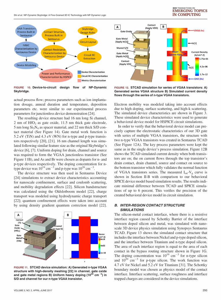
The n-type and p-type VGAA junctionless transistors wereextensively characterized using detailed physics-based 3Dsimulation of the electrostatics and operations using SynopsysSentaurus TCAD [22]. The Sentaurus Process [23] was usedto create the device structure (See Figure 11A) emulating
FIGURE 8. A) Schematic of NAND gate in NP-Dynamic Skybridge
B) Schematic of NOR gate in NP-Dynamic Skybridge C) Sche-
matic of NAND gate design in conventional 2D CMOS.
FIGURE 9. Normalized RC delay of NAND and NOR of DP-
Dynamic Skybridge, NAND of 2D CMOS and NAND of original
Skybridge.
292 VOLUME 5, NO. 2, APRIL-JUNE 2017
Shi et al.: NP-Dynamic Skybridge: A Fine-Grained 3D IC Technology with NP-Dynamic Logic
actual process flow; process parameters such as ion implanta-tion dosage, anneal duration and temperature, depositionparameters etc. were similar to our experimental processparameters for junctionless device demonstration [24].The resulting device structure had 16 nm long Si channel,
2 nm of HfO2 as gate oxide, 11.5 nm thick gate electrode,5 nm long Si3N4 as spacer material, and 22 nm thick S/D con-tact material (See Figure 14). Gate metal work function is5.2 eV (TiN) and 4.3 eV (WN) for n-type and p-type transis-tors respectively [20], [21]. 16 nm channel length was simu-lated following similar feature size as the original Skybridge’sdevice [6], [7]. Uniform doping for drain, channel and sourcewas required to form the VGAA junctionless transistor (SeeFigure 11B), and As and Br were chosen as dopants for n- andp-type devices respectively. The doping concentration for n-type device was 1019 cm�3 and p-type was 1020 cm�3.The device structure was then used in Sentaurus Device
[24] simulations to extract device characteristics accountingfor nanoscale confinement, surface and coulomb scattering,and mobility degradation effects [22]. Silicon bandstructurewas calculated using the Oldslotboom model [22], chargetransport was modeled using hydrodynamic charge transport[22]; quantum confinement effects were taken into accountby using density gradient quantum correction model [22].
Electron mobility was modeled taking into account effectsdue to high doping, surface scattering, and high-k scattering.The simulated device characteristics are shown in Figure 3.These simulated device characteristics were used to generatea behavioral device model for HSPICE circuit simulations.In order to verify that the behavioral device model can pre-
cisely capture the electrostatic characteristics of our 3D gatewith series of multiple VGAA transistors, the structure withtwo n-type VGAA transistors was created in Sentaurus TCAD(See Figure 12A). The key process parameters were kept thesame as in the single device’s process simulation. Figure 12Bshows the TCAD simulated current density when both transis-tors are on; the on current flows through the top transistor’sdrain contact, drain channel, source and contact on source tothe bottom transistor which fully validates the normal functionof VGAA transistors series. The measured Ion-Vg curve isshown in Section II-B with comparison to our behavioralSPICE device model based simulation results. The results indi-cate minimal difference between TCAD and SPICE simula-tions of up to 6 percent. This verifies the precision of thecreated behavioral device model in circuit simulation.
B. INTER-REGION CONTACT STRUCTURE
SIMULATIONS
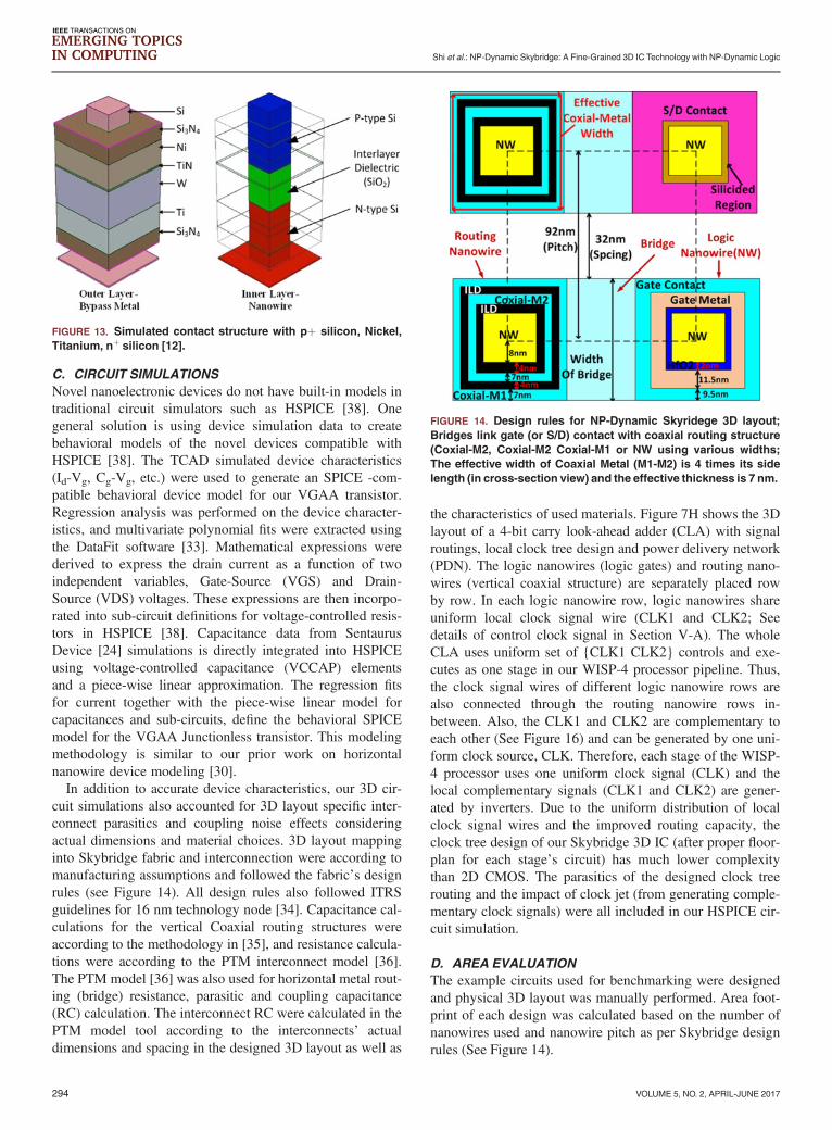
The silicon-metal contact interface, where there is a resistiveinterface region caused by Schottky Barrier of the interfacebetween doped silicon and metal, was simulated with nano-scale 3D device physics simulation using Synopsys SentaurusTCAD. Figure 13 shows the simulated contact structure thatincludes the interface betweenNickel and p-type doped silicon,and the interface between Titanium and n-type doped silicon.The area of each interface region is equal to the area of eachcontact in the bypass routing structure shown in Figure 1G.The doping concentration was 1019 cm�3 for n-type siliconand 1020 cm�3 for p-type silicon. The work function was4.7 eV for Nickel and 5.2 eV for Titanium [31]. The Schottkyboundary model was chosen as physics model of the contactinterface. Interface scattering, surface roughness and interfacetrapped charges are considered in the device simulations.
FIGURE 10. Device-to-circuit design flow of NP-Dynamic
Skybridge.
FIGURE 11. STCAD device simulation: A) Generated n-type VGAA
structure with high-density meshing [22] in channel, gate oxide
and gate metal regions B) Uniform heavy doping (1020 cm�3) in
S/D and channel for our n-type VGAA transistor.
FIGURE 12. STCAD simulation for series of VGAA transistors: A)
Generated series VGAA structure B) Simulated current density
flows through the series of n-type VGAA transistors.
VOLUME 5, NO. 2, APRIL-JUNE 2017 293
Shi et al.: NP-Dynamic Skybridge: A Fine-Grained 3D IC Technology with NP-Dynamic Logic
C. CIRCUIT SIMULATIONS
Novel nanoelectronic devices do not have built-in models intraditional circuit simulators such as HSPICE [38]. Onegeneral solution is using device simulation data to createbehavioral models of the novel devices compatible withHSPICE [38]. The TCAD simulated device characteristics(Id-Vg, Cg-Vg, etc.) were used to generate an SPICE -com-patible behavioral device model for our VGAA transistor.Regression analysis was performed on the device character-istics, and multivariate polynomial fits were extracted usingthe DataFit software [33]. Mathematical expressions werederived to express the drain current as a function of twoindependent variables, Gate-Source (VGS) and Drain-Source (VDS) voltages. These expressions are then incorpo-rated into sub-circuit definitions for voltage-controlled resis-tors in HSPICE [38]. Capacitance data from SentaurusDevice [24] simulations is directly integrated into HSPICEusing voltage-controlled capacitance (VCCAP) elementsand a piece-wise linear approximation. The regression fitsfor current together with the piece-wise linear model forcapacitances and sub-circuits, define the behavioral SPICEmodel for the VGAA Junctionless transistor. This modelingmethodology is similar to our prior work on horizontalnanowire device modeling [30].In addition to accurate device characteristics, our 3D cir-
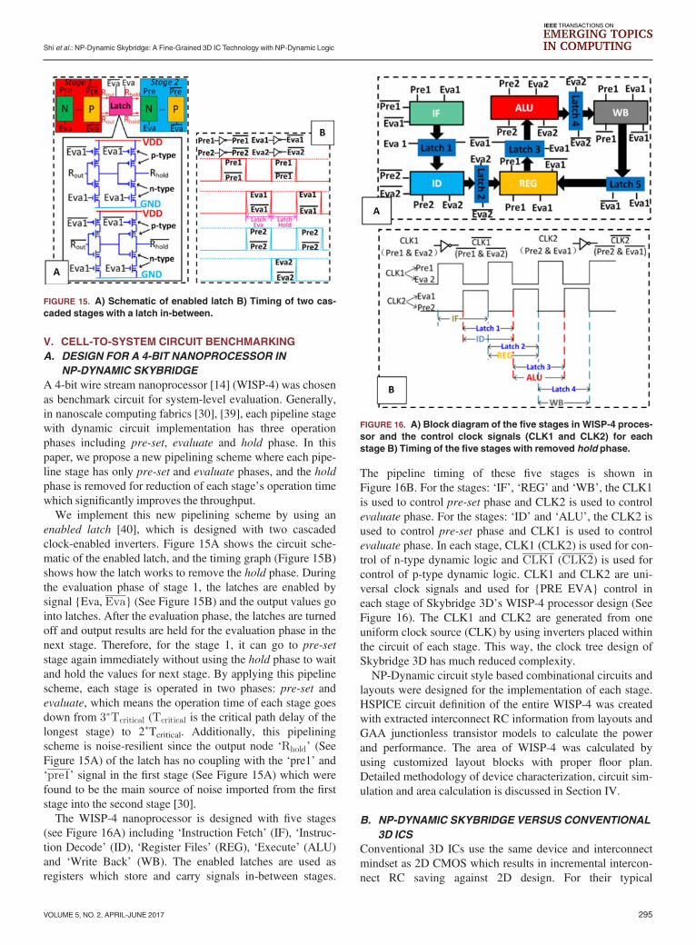
cuit simulations also accounted for 3D layout specific inter-connect parasitics and coupling noise effects consideringactual dimensions and material choices. 3D layout mappinginto Skybridge fabric and interconnection were according tomanufacturing assumptions and followed the fabric’s designrules (see Figure 14). All design rules also followed ITRSguidelines for 16 nm technology node [34]. Capacitance cal-culations for the vertical Coaxial routing structures wereaccording to the methodology in [35], and resistance calcula-tions were according to the PTM interconnect model [36].The PTM model [36] was also used for horizontal metal rout-ing (bridge) resistance, parasitic and coupling capacitance(RC) calculation. The interconnect RC were calculated in thePTM model tool according to the interconnects’ actualdimensions and spacing in the designed 3D layout as well as
the characteristics of used materials. Figure 7H shows the 3Dlayout of a 4-bit carry look-ahead adder (CLA) with signalroutings, local clock tree design and power delivery network(PDN). The logic nanowires (logic gates) and routing nano-wires (vertical coaxial structure) are separately placed rowby row. In each logic nanowire row, logic nanowires shareuniform local clock signal wire (CLK1 and CLK2; Seedetails of control clock signal in Section V-A). The wholeCLA uses uniform set of {CLK1 CLK2} controls and exe-cutes as one stage in our WISP-4 processor pipeline. Thus,the clock signal wires of different logic nanowire rows arealso connected through the routing nanowire rows in-between. Also, the CLK1 and CLK2 are complementary toeach other (See Figure 16) and can be generated by one uni-form clock source, CLK. Therefore, each stage of the WISP-4 processor uses one uniform clock signal (CLK) and thelocal complementary signals (CLK1 and CLK2) are gener-ated by inverters. Due to the uniform distribution of localclock signal wires and the improved routing capacity, theclock tree design of our Skybridge 3D IC (after proper floor-plan for each stage’s circuit) has much lower complexitythan 2D CMOS. The parasitics of the designed clock treerouting and the impact of clock jet (from generating comple-mentary clock signals) were all included in our HSPICE cir-cuit simulation.
D. AREA EVALUATION
The example circuits used for benchmarking were designedand physical 3D layout was manually performed. Area foot-print of each design was calculated based on the number ofnanowires used and nanowire pitch as per Skybridge designrules (See Figure 14).
FIGURE 13. Simulated contact structure with pþ silicon, Nickel,
Titanium, nþ silicon [12].
FIGURE 14. Design rules for NP-Dynamic Skyridege 3D layout;
Bridges link gate (or S/D) contact with coaxial routing structure
(Coxial-M2, Coxial-M2 Coxial-M1 or NW using various widths;
The effective width of Coaxial Metal (M1-M2) is 4 times its side
length (in cross-section view) and the effective thickness is 7 nm.
294 VOLUME 5, NO. 2, APRIL-JUNE 2017
Shi et al.: NP-Dynamic Skybridge: A Fine-Grained 3D IC Technology with NP-Dynamic Logic
V. CELL-TO-SYSTEM CIRCUIT BENCHMARKING
A. DESIGN FOR A 4-BIT NANOPROCESSOR IN
NP-DYNAMIC SKYBRIDGE
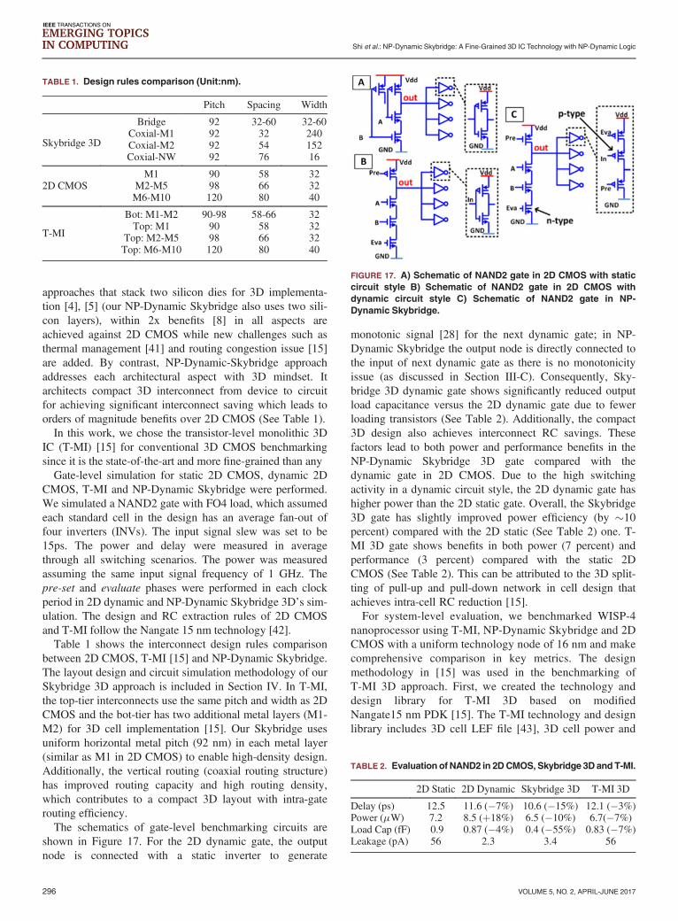
A 4-bit wire stream nanoprocessor [14] (WISP-4) was chosenas benchmark circuit for system-level evaluation. Generally,in nanoscale computing fabrics [30], [39], each pipeline stagewith dynamic circuit implementation has three operationphases including pre-set, evaluate and hold phase. In thispaper, we propose a new pipelining scheme where each pipe-line stage has only pre-set and evaluate phases, and the holdphase is removed for reduction of each stage’s operation timewhich significantly improves the throughput.We implement this new pipelining scheme by using an
enabled latch [40], which is designed with two cascadedclock-enabled inverters. Figure 15A shows the circuit sche-matic of the enabled latch, and the timing graph (Figure 15B)shows how the latch works to remove the hold phase. Duringthe evaluation phase of stage 1, the latches are enabled bysignal {Eva, Eva} (See Figure 15B) and the output values gointo latches. After the evaluation phase, the latches are turnedoff and output results are held for the evaluation phase in thenext stage. Therefore, for the stage 1, it can go to pre-setstage again immediately without using the hold phase to waitand hold the values for next stage. By applying this pipelinescheme, each stage is operated in two phases: pre-set andevaluate, which means the operation time of each stage goesdown from 3�Tcritical (Tcritical is the critical path delay of thelongest stage) to 2�Tcritical. Additionally, this pipeliningscheme is noise-resilient since the output node ‘Rhold’ (SeeFigure 15A) of the latch has no coupling with the ‘pre1’ and‘pre1’ signal in the first stage (See Figure 15A) which werefound to be the main source of noise imported from the firststage into the second stage [30].The WISP-4 nanoprocessor is designed with five stages
(see Figure 16A) including ‘Instruction Fetch’ (IF), ‘Instruc-tion Decode’ (ID), ‘Register Files’ (REG), ‘Execute’ (ALU)and ‘Write Back’ (WB). The enabled latches are used asregisters which store and carry signals in-between stages.
The pipeline timing of these five stages is shown inFigure 16B. For the stages: ‘IF’, ‘REG’ and ‘WB’, the CLK1is used to control pre-set phase and CLK2 is used to controlevaluate phase. For the stages: ‘ID’ and ‘ALU’, the CLK2 isused to control pre-set phase and CLK1 is used to controlevaluate phase. In each stage, CLK1 (CLK2) is used for con-trol of n-type dynamic logic and CLK1 (CLK2) is used forcontrol of p-type dynamic logic. CLK1 and CLK2 are uni-versal clock signals and used for {PRE EVA} control ineach stage of Skybridge 3D’s WISP-4 processor design (SeeFigure 16). The CLK1 and CLK2 are generated from oneuniform clock source (CLK) by using inverters placed withinthe circuit of each stage. This way, the clock tree design ofSkybridge 3D has much reduced complexity.NP-Dynamic circuit style based combinational circuits and
layouts were designed for the implementation of each stage.HSPICE circuit definition of the entire WISP-4 was createdwith extracted interconnect RC information from layouts andGAA junctionless transistor models to calculate the powerand performance. The area of WISP-4 was calculated byusing customized layout blocks with proper floor plan.Detailed methodology of device characterization, circuit sim-ulation and area calculation is discussed in Section IV.
B. NP-DYNAMIC SKYBRIDGE VERSUS CONVENTIONAL
3D ICS
Conventional 3D ICs use the same device and interconnectmindset as 2D CMOS which results in incremental intercon-nect RC saving against 2D design. For their typical
FIGURE 16. A) Block diagram of the five stages in WISP-4 proces-
sor and the control clock signals (CLK1 and CLK2) for each
stage B) Timing of the five stages with removed hold phase.
FIGURE 15. A) Schematic of enabled latch B) Timing of two cas-
caded stages with a latch in-between.
VOLUME 5, NO. 2, APRIL-JUNE 2017 295
Shi et al.: NP-Dynamic Skybridge: A Fine-Grained 3D IC Technology with NP-Dynamic Logic
approaches that stack two silicon dies for 3D implementa-tion [4], [5] (our NP-Dynamic Skybridge also uses two sili-con layers), within 2x benefits [8] in all aspects areachieved against 2D CMOS while new challenges such asthermal management [41] and routing congestion issue [15]are added. By contrast, NP-Dynamic-Skybridge approachaddresses each architectural aspect with 3D mindset. Itarchitects compact 3D interconnect from device to circuitfor achieving significant interconnect saving which leads toorders of magnitude benefits over 2D CMOS (See Table 1).In this work, we chose the transistor-level monolithic 3D
IC (T-MI) [15] for conventional 3D CMOS benchmarkingsince it is the state-of-the-art and more fine-grained than anyGate-level simulation for static 2D CMOS, dynamic 2D
CMOS, T-MI and NP-Dynamic Skybridge were performed.We simulated a NAND2 gate with FO4 load, which assumedeach standard cell in the design has an average fan-out offour inverters (INVs). The input signal slew was set to be15ps. The power and delay were measured in averagethrough all switching scenarios. The power was measuredassuming the same input signal frequency of 1 GHz. Thepre-set and evaluate phases were performed in each clockperiod in 2D dynamic and NP-Dynamic Skybridge 3D’s sim-ulation. The design and RC extraction rules of 2D CMOSand T-MI follow the Nangate 15 nm technology [42].Table 1 shows the interconnect design rules comparison
between 2D CMOS, T-MI [15] and NP-Dynamic Skybridge.The layout design and circuit simulation methodology of ourSkybridge 3D approach is included in Section IV. In T-MI,the top-tier interconnects use the same pitch and width as 2DCMOS and the bot-tier has two additional metal layers (M1-M2) for 3D cell implementation [15]. Our Skybridge usesuniform horizontal metal pitch (92 nm) in each metal layer(similar as M1 in 2D CMOS) to enable high-density design.Additionally, the vertical routing (coaxial routing structure)has improved routing capacity and high routing density,which contributes to a compact 3D layout with intra-gaterouting efficiency.The schematics of gate-level benchmarking circuits are
shown in Figure 17. For the 2D dynamic gate, the outputnode is connected with a static inverter to generate
monotonic signal [28] for the next dynamic gate; in NP-Dynamic Skybridge the output node is directly connected tothe input of next dynamic gate as there is no monotonicityissue (as discussed in Section III-C). Consequently, Sky-bridge 3D dynamic gate shows significantly reduced outputload capacitance versus the 2D dynamic gate due to fewerloading transistors (See Table 2). Additionally, the compact3D design also achieves interconnect RC savings. Thesefactors lead to both power and performance benefits in theNP-Dynamic Skybridge 3D gate compared with thedynamic gate in 2D CMOS. Due to the high switchingactivity in a dynamic circuit style, the 2D dynamic gate hashigher power than the 2D static gate. Overall, the Skybridge3D gate has slightly improved power efficiency (by �10percent) compared with the 2D static (See Table 2) one. T-MI 3D gate shows benefits in both power (7 percent) andperformance (3 percent) compared with the static 2DCMOS (See Table 2). This can be attributed to the 3D split-ting of pull-up and pull-down network in cell design thatachieves intra-cell RC reduction [15].For system-level evaluation, we benchmarked WISP-4
nanoprocessor using T-MI, NP-Dynamic Skybridge and 2DCMOS with a uniform technology node of 16 nm and makecomprehensive comparison in key metrics. The designmethodology in [15] was used in the benchmarking ofT-MI 3D approach. First, we created the technology anddesign library for T-MI 3D based on modifiedNangate15 nm PDK [15]. The T-MI technology and designlibrary includes 3D cell LEF file [43], 3D cell power and
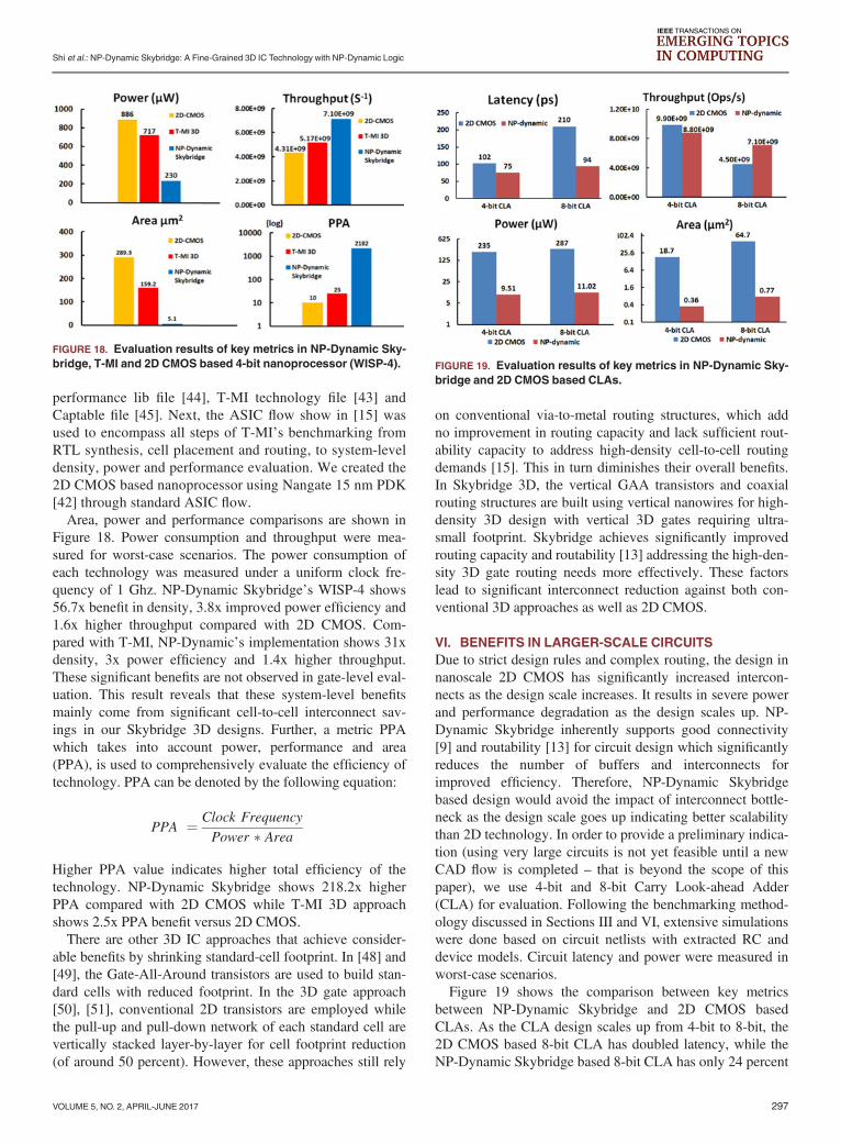
TABLE 1. Design rules comparison (Unit:nm).
Pitch Spacing Width
Skybridge 3D
Bridge 92 32-60 32-60Coxial-M1 92 32 240Coxial-M2 92 54 152Coxial-NW 92 76 16
2D CMOSM1 90 58 32
M2-M5 98 66 32M6-M10 120 80 40
T-MI
Bot: M1-M2 90-98 58-66 32Top: M1 90 58 32
Top: M2-M5 98 66 32Top: M6-M10 120 80 40
FIGURE 17. A) Schematic of NAND2 gate in 2D CMOS with static
circuit style B) Schematic of NAND2 gate in 2D CMOS with
dynamic circuit style C) Schematic of NAND2 gate in NP-
Dynamic Skybridge.
TABLE 2. Evaluation of NAND2 in 2DCMOS,Skybridge 3D andT-MI.
2D Static 2D Dynamic Skybridge 3D T-MI 3D
Delay (ps) 12.5 11.6 (�7%) 10.6 (�15%) 12.1 (�3%)Power (mW) 7.2 8.5 (þ18%) 6.5 (�10%) 6.7(�7%)Load Cap (fF) 0.9 0.87 (�4%) 0.4 (�55%) 0.83 (�7%)Leakage (pA) 56 2.3 3.4 56
296 VOLUME 5, NO. 2, APRIL-JUNE 2017
Shi et al.: NP-Dynamic Skybridge: A Fine-Grained 3D IC Technology with NP-Dynamic Logic
performance lib file [44], T-MI technology file [43] andCaptable file [45]. Next, the ASIC flow show in [15] wasused to encompass all steps of T-MI’s benchmarking fromRTL synthesis, cell placement and routing, to system-leveldensity, power and performance evaluation. We created the2D CMOS based nanoprocessor using Nangate 15 nm PDK[42] through standard ASIC flow.Area, power and performance comparisons are shown in
Figure 18. Power consumption and throughput were mea-sured for worst-case scenarios. The power consumption ofeach technology was measured under a uniform clock fre-quency of 1 Ghz. NP-Dynamic Skybridge’s WISP-4 shows56.7x benefit in density, 3.8x improved power efficiency and1.6x higher throughput compared with 2D CMOS. Com-pared with T-MI, NP-Dynamic’s implementation shows 31xdensity, 3x power efficiency and 1.4x higher throughput.These significant benefits are not observed in gate-level eval-uation. This result reveals that these system-level benefitsmainly come from significant cell-to-cell interconnect sav-ings in our Skybridge 3D designs. Further, a metric PPAwhich takes into account power, performance and area(PPA), is used to comprehensively evaluate the efficiency oftechnology. PPA can be denoted by the following equation:
PPA ¼ Clock Frequency
Power � Area
Higher PPA value indicates higher total efficiency of thetechnology. NP-Dynamic Skybridge shows 218.2x higherPPA compared with 2D CMOS while T-MI 3D approachshows 2.5x PPA benefit versus 2D CMOS.There are other 3D IC approaches that achieve consider-
able benefits by shrinking standard-cell footprint. In [48] and[49], the Gate-All-Around transistors are used to build stan-dard cells with reduced footprint. In the 3D gate approach[50], [51], conventional 2D transistors are employed whilethe pull-up and pull-down network of each standard cell arevertically stacked layer-by-layer for cell footprint reduction(of around 50 percent). However, these approaches still rely
on conventional via-to-metal routing structures, which addno improvement in routing capacity and lack sufficient rout-ability capacity to address high-density cell-to-cell routingdemands [15]. This in turn diminishes their overall benefits.In Skybridge 3D, the vertical GAA transistors and coaxialrouting structures are built using vertical nanowires for high-density 3D design with vertical 3D gates requiring ultra-small footprint. Skybridge achieves significantly improvedrouting capacity and routability [13] addressing the high-den-sity 3D gate routing needs more effectively. These factorslead to significant interconnect reduction against both con-ventional 3D approaches as well as 2D CMOS.
VI. BENEFITS IN LARGER-SCALE CIRCUITS
Due to strict design rules and complex routing, the design innanoscale 2D CMOS has significantly increased intercon-nects as the design scale increases. It results in severe powerand performance degradation as the design scales up. NP-Dynamic Skybridge inherently supports good connectivity[9] and routability [13] for circuit design which significantlyreduces the number of buffers and interconnects forimproved efficiency. Therefore, NP-Dynamic Skybridgebased design would avoid the impact of interconnect bottle-neck as the design scale goes up indicating better scalabilitythan 2D technology. In order to provide a preliminary indica-tion (using very large circuits is not yet feasible until a newCAD flow is completed – that is beyond the scope of thispaper), we use 4-bit and 8-bit Carry Look-ahead Adder(CLA) for evaluation. Following the benchmarking method-ology discussed in Sections III and VI, extensive simulationswere done based on circuit netlists with extracted RC anddevice models. Circuit latency and power were measured inworst-case scenarios.Figure 19 shows the comparison between key metrics
between NP-Dynamic Skybridge and 2D CMOS basedCLAs. As the CLA design scales up from 4-bit to 8-bit, the2D CMOS based 8-bit CLA has doubled latency, while theNP-Dynamic Skybridge based 8-bit CLA has only 24 percent
FIGURE 18. Evaluation results of key metrics in NP-Dynamic Sky-
bridge, T-MI and 2D CMOS based 4-bit nanoprocessor (WISP-4). FIGURE 19. Evaluation results of key metrics in NP-Dynamic Sky-
bridge and 2D CMOS based CLAs.
VOLUME 5, NO. 2, APRIL-JUNE 2017 297
Shi et al.: NP-Dynamic Skybridge: A Fine-Grained 3D IC Technology with NP-Dynamic Logic
increase in latency. In terms of active power, the NP-DynamicSkybridge based 8-bit CLA only has 16 percent increasedpower while the 2D CMOS based version has 25 percentincreased power with respect to corresponding 4-bit CLAimplementation. The throughput of NP-Dynamic Skybridgebased 8-bit CLA decreases by 20 percent while the 2D CMOSversion has 50 percent decreased throughput compared withthe 4-bit CLAs respectively. These results indicate that NP-Dynamic Skybridge is impacted to a lesser degree comparedto 2D CMOS as the circuit design scales up in bit-width, indi-cating that Skybridge can potentially have significant benefitsagainst 2D CMOS for large-scale designs.
VII. CONCLUSION
In this paper, we detailed a new vertical nanowire based3D integrated circuits fabric called NP-Dynamic Sky-bridge. Fabric’s core components and device-to-circuitevaluations were shown. By using both n- and p-type tran-sistors, NP-Dynamic Skybridge offers a wide range of ele-mentary logics for improved implementation efficiency.Additionally, a new pipeline scheme was proposed for sim-plified operation of pipeline stages and improves through-put. Benchmarking of a 4-bit nanoprocessor showed 56.7xbenefit in density, 3.8x improved power efficiency and1.6x increased throughput versus 2D CMOS, and 31x den-sity, 3x power efficiency and 1.4x throughput benefitscompared to transistor-level monolithic CMOS 3D IC. Wealso investigated the impact of increasing bit-width on cir-cuit metrics for CLAs, which showed that NP-DynamicSkybridge was less affected than 2D and 3D CMOS indi-cating its potential for scalability. Further work is ongoingincluding CAD flow, CAD-based designs and experimentalprototyping.
ACKNOWLEDGMENTS
This work was supported in part by the Center for Hierarchi-cal Manufacturing (CHM) at UMass Amherst, and NSFawards (Award Number: 140796).
REFERENCES
[1] H. lwai, “Roadmap for 22 nm and beyond,” Microelectronic Eng., vol. 86,pp. 1520–1528, 2009.
[2] K. Kim, K. K. Das, R. V. Joshi, and C. Chuang, “Nanoscale CMOS circuitleakage power reduction by double-gate device,” in Proc. Int. Symp. LowPower Electron. Des., 2004, pp. 102–107.
[3] J. Warnock, “Circuit design challenges at the 14 nm technology node,” inProc. 48th Des. Autom. Conf., 2011, pp. 464–467.
[4] S. Lim, “3D circuit design with through-silicon-via: Challenges and oppor-tunities,” IEEE EDP, 2010.
[5] S. Panth, S. Samal, Y. S. Yu, and S. K. Lim, “Design challenges and solu-tions for ultra-high-density monolithic 3D ICs,” J. Inf. Commun. Conver-gence Eng., vol. 12, pp. 186–192, 2014.
[6] M. Rahman, et al., “Fine-grained 3-D integrated circuit fabric using verti-cal nanowires,” in Proc. Int. 3D Syst. Integr. Conf., 2015, pp. TS9.3.1–TS9.3.7.
[7] M. Rahman, et al., “Skybridge: 3-D integrated circuit technology alterna-tive to CMOS,” 2014. [Online]. Available: http://arxiv.org/abs/1404.0607
[8] D. K. Nayak, et al., “Power, performance, and cost comparisons of mono-lithic 3D ICs and TSV-based 3D ICs,” in Proc. IEEE SOI-3D-Subthresh-old Microelectronics Technol. Unified Conf., 2015, pp. 1–2.
[9] S. Khasanvis, et al., “Architecting connectivity for fine-grained 3-D verti-cally integrated circuits,” in Proc. IEEE/ACM Int. Symp. NanoscaleArchit., 2015, pp. 175–180.
[10] M. Rahman, et al., “Architecting 3-D integrated circuit fabric with intrinsicthermal management features,” in Proc. IEEE/ACM Int. Symp. NanoscaleArchit., 2015, pp. 186–192.
[11] M. Rahman, et al., “Manufacturing Pathway and Experimental Demonstra-tion for Nanoscale Fine-Grained 3-D Integrated Circuit Fabric,” in Proc.IEEE 15th Int. Conf. Nanotechnology, 2015, pp. 1214–1217.
[12] J. Shi, et al., “Architecting NP-Dynamic Skybridge,” in Proc. IEEE/ACMInt. Symp. Nanoscale Archit., 2015, pp. 169–174.
[13] J. Shi et al., “Routability in 3D IC design: Monolithic 3D versus Skybridge3D CMOS,” in Proc. IEEE/ACM Int. Symp. Nanoscale Archit., 2015,pp. 145–150.
[14] C. A. Moritz and T. Wang, “Towards defect-tolerant nanoscale architec-tures,” in Proc. IEEE 15th Int. Conf. Nanotechnology, 2006, pp. 331–334.
[15] Y. Lee, et al., “Power benefit study for ultra-high density transistor-levelmonolithic 3D ICs,” in Proc. 50th ACM/EDAC/IEEE Des. Autom. Conf.,2013, pp. 1–10.
[16] P. Batude, et al., “Advances in 3D CMOS sequential integration,” in Proc.IEEE Int. Electron Dev. Meet., 2009, pp. 1–4.
[17] P. Batude, et al., “Demonstration of low temperature 3D sequential FDSOIintegration down to 50 nm gate length,” in Proc. Symp. VLSI Technol.,2011, pp. 158–159.
[18] M. M. Mirza, et al., “Nanofabrication of high aspect ratio (�50:1) sub-10nm silicon nanowires using inductively coupled plasma etching,” J. Vac.Sci. Technol., vol. 30, 2012, Art. no. 06FF02.
[19] A. Kranti, et al., “Junctionless nanowire transistor (JNT): Properties anddesign guidelines,” in Proc. Eur. Solid State Device Res. Conf., 2010,pp. 158–159.
[20] K. Choi, et al., “The effect of metal thickness, Overlayer and High-k sur-face treatment on the effective work function of metal electrode,” in Proc.Eur. Solid State Device Res. Conf., 2005, pp. 101–104.
[21] P. Jiang, et al., “Dependence of crystal structure and work function ofWNx films on the nitrogen content,” Appl. Phys. Lett., vol. 89, pp.122107–122107 -3, 2006.
[22] “Synopsys- Sentaurus User Guide,” 2015-1.[23] “Synopsys- Sentaurus Process User Guide,” 2012-SP1.[24] “Synopsys- Sentaurus Device User Guide,” 2012-SP1.[25] M. Rahman, et al., “Experimental prototyping of beyond-CMOS nanowire
computing fabrics,” in Proc. IEEE/ACM Int. Symp. Nanoscale Archit.,2013, pp. 134–139.
[26] W. B. Nowak, R. Keukelaar, W. Wang, and A. R. Nyaiesh, “Diffusion ofNickel through Titanium nitride films,” J. Vacuum Sci. Technol., vol. 3,pp. 2242–2245, 1985.
[27] R. S. Rosler, et al., “Tungsten chemical vapor deposition characteristicsusing SiH4 in a single wafer system,” J. Vacuum Sci. Technol., vol. 6,pp. 1721–1727, 1988.
[28] N. Weste and D. Harris, CMOS VLSI Design: A Circuits and Systems Per-spective, Boston, MA, USA: Addison Wesley, 2011.
[29] Arizona State University, PTM-MG device models for 16nm node,[Online]. Available: www.ptm.asu.edu.
[30] P. Narayanan, J. Kina, P. Panchapakeshan, C. O. Chui, and C. A.Moritz, “Integrated device–fabric explorations and noise mitigation innanoscale fabrics,” IEEE Trans. Nanotech., vol. 11, no. 4, pp. 687–700, Jul. 2012.
[31] CRC Handbook of Chemistry and Physics. Boca Raton, FL, USA: CRCPress, 2008, pp. 12–114.
[32] G. Pei, et al., “FinFET design considerations based on 3-D simulation andanalytical modeling,” IEEE Trans. Elect. Dev., vol. 49, no. 8, pp. 1411–1419, Aug. 2002
[33] Oakdale Engineering, DataFit Software. Version 9.0, 2013. [Online].Available: http://www.oakdaleengr.com/download.htm
[34] ITRS, ITRS Lithography Tables, 2015. [Online]. Available: http://itrs.net/[35] A. Milovanovic and B. Koprivica, “Analysis of square coaxial lines by
using equivalent electrodes method,” in Proc. Joint 3rd Int. WorkshopNonlinear Dynamics Synchronization 16th Int. Symp. Theoretical Electr.Eng., 2011, pp. 1–6.
[36] Arizona State University, PTM R-C Interconnect models, 2012. [Online].Available: http://ptm.asu.edu/
[37] T. Solankia and N. Parmar, “A Review paper: A Comprehensive study ofJunctionless transistor,” in Proc. IEEE Natl. Conf. Recent TrendsEng. Technol., 2012.
[38] “HSPICE simulation and analysis guide” 2009.
298 VOLUME 5, NO. 2, APRIL-JUNE 2017
Shi et al.: NP-Dynamic Skybridge: A Fine-Grained 3D IC Technology with NP-Dynamic Logic
[39] P. Narayanan, et al., “CMOS control enabled single-type FET NASIC,” inProc. IEEE Comput. Soc. Annu. Symp. VLSI, 2008, pp. 191–196.
[40] N. F. Goncalves and H. De Man, “NORA: A racefree dynamic CMOStechnique for pipelined logic structures,” IEEE J. Solid-State Circuits, vol.18, no. 3, pp. 261–266, Jun. 1983.
[41] S. Samal, et al., “Fast and accurate thermal modeling and optimization formonolithic 3D ICs,” in Proc. 51st ACM/EDAC/IEEE Des. Autom. Conf.,2014, pp. 1–6.
[42] Nangate, Nangate 15 nm Open Cell Library.[43] “LEF/DEF Language Reference,” 2011.[44] “Liberty user guides and reference manual suite” 2013.[45] QRC Extraction Users Manual, Cadence, San Jose, CA, USA, 2010.[46] R. Rios, et al., “Comparison of junctionless and conventional trigate tran-
sistors with Lg down to 26 nm,” IEEE Electron Dev. Lett., vol. 32, no. 9,pp. 1170–1172, Sep. 2011.
[47] A. Veloso, “Challenges and opportunities of vertical FET devices using 3Dcircuit design layouts,” in Proc. IEEE SOI-3D-Subthreshold Microelec-tronics Technol. Unified Conf., 2016, pp. 1–3.
[48] W.-C. Wang and P. Gupta, “Efficient layout generation and design evalua-tion of vertical channel devices,” IEEE Trans. Comput.-Aided Des. Integr.Circuits Syst., vol. 35, no. 9, pp. 1449–1460, Sep. 2016.
[49] C. Pan, et al., “Technology/System Codesign and benchmarking for lateraland vertical GAA nanowire FETs at 5-nm technology node,” IEEE Trans.Elect. Dev., vol. 62, no. 10, pp. 3125–3132, Oct. 2015.
[50] A. B. Sachid, et al., “Monolithic 3D CMOS using layered semiconduc-tors,” Adv. Materials, vol. 28, no. 13, pp. 2547–2554, 2016.
[51] G. Roos and B. Hoefflinger, “Complex 3D CMOS circuits based on atriple-decker cell,” IEEE Journal of Solid-State Circuits, vol. 27, no. 7,pp. 1067–1072, 1992.
JIAJUN SHI received the BEng degree from Uni-versity of Electronic Science and Technology ofChina, Chengdu, China, in 2012, and the MSdegree in computer engineering from University ofMassachusetts Amherst, in 2014. He is currently aresearch assistant in Nanoscale Computing Fabricslab in University of Massachusetts, Amherst. He iscurrently working toward the PhD degree in com-puter engineering at UMass Amherst. His researchhas appeared in IEEE/ACM NANOARCH 2015and 2016, ISVLSI 2016 and IEDM 2017. He is a
reviewer for the IEEE Transactions on Nanotechnology. His research inter-ests include nanoscale 3-D integration, beyond CMOS computer architec-tures, emerging devices and nanoscale fabrication.
MINGYU LI received the BS degree in automa-tion engineering from the Shandong University,Jinan, China, and the MSECE degree from Uni-versity of Massachusetts Amherst, in 2012 and2015, respectively. He is currently workingtoward the PhD degree in electrical and computerengineering at University of Massachusetts,Amherst. He is a research assistant in NanoscaleComputing Fabrics lab, UMass. He has publishedhis research in several peer-reviewed IEEE, ACMjournals and conferences, where he also contrib-
utes as a reviewer. His research interests include 3D integration technologyand post-CMOS computing fabrics.
MOSTAFIZUR RAHMAN joined the ComputerScience and Electrical Engineering (CSEE) Depart-ment at University of Missouri Kansas City afterreceiving the PhD degree from University of Mas-sachusetts Amherst in electrical and computer engi-neering. He leads the Nanoscale Integrated Circuits(Nano-IC) lab and is a co-lead for the Center forInterdisciplinary Nanoscale Research (CINTR) atCSEE. His group’s research focus is on transforma-tive approaches for nanoelectronics to surpass thecurrent limitations of today’s integrated circuits. He
is currently serving as publication chair for NANOARCH and guest editorfor special issue of the IEEE Transactions on Nanotechnology. He is also aprogram committee member for NANOARCH and VLSIDESIGN conferen-ces. In addition, he serves as a reviewer for TNANO, JETC, JPDC, NANO-ARCH and other publications.
SANTOSH KHASANVIS received the PhD degree in computer engineer-ing from University of Massachusetts, Amherst, in 2015. He is a seniorresearch scientist with BlueRISC Inc. This work was performed during thePhD degree. His research interests include unconventional computing archi-tectures, nanoscale computing, and cyber-security. He is a member of theIEEE since 2015.
CSABA ANDRAS MORITZ received the PhDdegree in computer systems from the Royal Insti-tute of Technology, Stockholm, Sweden, in 1998.From 1997 to 2000, he was a research scientistwith Laboratory for Computer Science, the Massa-chusetts Institute of Technology (MIT), Cam-bridge. He has consulted for several technologycompanies in Scandinavia and held industrial posi-tions ranging from CEO, to CTO, and to founder.His most recent company, BlueRISC Inc, developssecurity microprocessors and hardware-assisted
security solutions for anti tamper, cyber defense, hardware assisted securityand system assurance. He is currently a professor with the Department ofElectrical and Computer Engineering, University of Massachusetts,Amherst. His current research interests include NANO electronics and nano-scale systems, computer architecture, and security.
VOLUME 5, NO. 2, APRIL-JUNE 2017 299
Shi et al.: NP-Dynamic Skybridge: A Fine-Grained 3D IC Technology with NP-Dynamic Logic