novel zero voltage switching dual-switch forward converter with ripple current cancellation
TRANSCRIPT
Novel zero voltage switching dual-switch forwardconverter with ripple current cancellation
B.R. Lin, C.L. Huang and M.Y. Li
Abstract: A zero voltage switching (ZVS) dual-switch forward converter with ripple current can-cellation is presented. In the proposed converter, active clamp circuit is used to clamp the voltagestresses and to realise ZVS of all switching devices. Active clamp boost converter with powerfactor correction is used in the front stage of the proposed converter to draw a sinusoidal linecurrent from the AC source and to maintain a constant voltage at the DC bus. The second stageof the proposed converter is a dual-switch forward converter with current doubler rectifier toobtain the isolated low output voltage. Active clamp circuit used in the DC/DC converter canrecycle the energy stored in the leakage inductor and magnetising inductor so that the voltage stres-ses on the switches are limited and the ZVS feature is realised. The current doubler rectifier offersthe ripple current cancellation at the output capacitor and reduces the current stress of the transfor-mer secondary winding. The circuit configuration and principle of operation are analysed and dis-cussed in detail. Experimental results with a laboratory prototype based on a 90–260 Vrms inputand 12 V/30 A output were provided to verify the effectiveness of the proposed converter.
1 Introduction
Because of the development of power devices,high-frequency power converters have been used in indus-trial applications and home electronic equipment. To meetthe international standard IEC 1000-3-2, active currentshaping techniques [1–3] have been proposed to improvepower factor and obtain a stable DC-link voltage. Boostconverter is used as the front stage in the switching modepower supplies (SMPS) with the feature of power factorcorrection (PFC). The second stage of the conventionalSMPS is forward or flyback converter with dual-switchtopology. However, the power switches are operated inthe hard switching and the available duty cycle is lessthan 50%. Soft switching dual-switch forward convertershave been proposed in [4–7] to reduce switching losseson power switches. Active clamp technique [8–10] is oneof the most attractive ZVS techniques in the DC/DCconverters. The leakage inductor and output capacitor ofswitching devices are resonant to achieve ZVS turn-on ofpower switches. The current doubler rectifier [11, 12] hasthe advantages of low current rating of the transformersecondary winding and low output voltage ripple at theoutput capacitor.A novel dual-switch forward converter with ripple
current cancellation is presented in Fig. 1. In the proposedconverter, the front stage is an AC/DC converter withactive clamp topology to achieve PFC, regulate DC-linkvoltage and achieve zero voltage switching (ZVS) ofswitching devices. The second stage of the proposedconverter is a dual-switch forward converter with current
# The Institution of Engineering and Technology 2007
doi:10.1049/iet-epa:20060434
Paper first received 27th October 2006 and in revised form 22nd January 2007
The authors are with the Department of Electrical Engineering, PowerElectronics Research Laboratory, National Yunlin University of Science andTechnology, Yunlin 640, Taiwan, Republic of China
E-mail: [email protected]
IET Electr. Power Appl., 2007, 1, (5), pp. 799–807
doubler rectifier to obtain the isolated output voltage andachieve ripple current cancellation. Active clamp circuit isused in the DC/DC converter to absorb the energy storedin the leakage inductor and magnetising inductor so thatthe voltage stresses of switches are limited. First, thecircuit configuration of the proposed converter is discussed.The principle of operation and mathematical analysis of theproposed converter in each operation stages are presented indetail. The design consideration of the converter is alsoprovided. Finally, the experimental results of a laboratoryprototype with 360 W rated power are provided to verifythe effectiveness of the proposed converter.
2 Proposed ZVS AC/DC converter
2.1 Circuit analysis and operation principle
The front stage of the proposed converter shown in Fig. 1 isa boost converter with buck-boost type of active clamp torealise PFC and achieve ZVS turn-on of switchingdevices. The AC/DC converter includes diode rectifier, L,Q1, D and CDC. Cr1 is a resonant capacitor. The resonantinductor Lr1, clamp capacitor C1 and auxiliary switch Q2
are connected in parallel with the boost inductor L tocreate a resonance. The main and auxiliary switches areswitched in a complementary way with a time delay.When switch Q1 is turned off, the positive inductorcurrent iLr1 will flow through clamp capacitor C1 andanti-parallel diode of auxiliary switch Q2. Therefore thedrain voltage of auxiliary switch vQ2,ds
is zero. At thisinstant, auxiliary switch can be turned on to realise ZVS.If switch Q2 is turned on, the inductor voltage acrossresonant inductor Lr1 is negative, then inductor current iLr1decreases from positive to negative value. When switchQ2 is turned off, the negative inductor current iLr1 willflow through resonant capacitor Cr1. Therefore the capacitorvoltage vCr1
is discharged from positive voltage to zero.When the capacitor voltage vCr1
¼ 0 and the inductorcurrent iLr1 , 0, the anti-parallel diode of main switch Q1
799

Fig. 1 Proposed active clamp converter with PFC
is turned on. Then the main switch Q1 can be turned on atthis instant to achieve ZVS.
Before the discussion of the principles of operation, it isassumed that all components of the proposed AC/DCconverter are ideal and the switching frequency fs of switch-ing devices is higher than the line frequency fL of utilityvoltage. The rectified voltage vin can be considered to bea constant voltage during one switching period. Thereforethe AC source and diode rectifier are not considered inthe system analysis. The capacitance CDC and clamp capaci-tance C1 are large enough so that the voltages vDC and vC1
are constant during one switching cycle. The inductanceof inductor L is greater than the inductance of Lr1. Theenergy stored in the resonant inductor Lr1 is greater thanenergy stored in the resonant capacitor Cr1 to realise ZVSturn-on of main switch Q1. The circuit behaviour of theproposed AC/DC converter during one switching cyclecan be divided into six operating stages. Figs. 2 and 3give the equivalent circuits of six operating stages and thetime sequence of key waveforms in the proposed AC/DCconverter, respectively. The duty cycle D is based on themain switch Q1.
Stage 1 (t0 , t , t1): Switch Q1 is turned on and Q2 isturned off during this stage. The input inductor voltage vLand resonant inductor voltage vLr1 equal input voltage vin.
800
Since vDC . vin, diode D is turned off and diode currentiD ¼ 0. The input power is stored in the inductors L andLr1. The inductor currents iLr1 and iL increase linearlyduring this stage. The switch currents iQ1
¼ iLr1 andiQ2
¼ 0. This stage ends at t1 when main switch Q1 isturned off.
Stage 2 (t1 , t , t2): In this stage, main switch Q1 is turnedoff at t1. The positive inductor current iLr1 flows through Cr1
so that capacitor voltage vCr1increases from zero voltage to
vDC � iLr1 ’ vDC. The capacitor voltage vCr1and inductor
current iLr1 can be expressed as
vCr1(t) ’
iLr (t1)(t � t1)
Cr1
iLr1 (t) ’ iLr1 (t1)þvin(t � t1)
Lþ Lr1(1)
In this stage, the capacitor voltage vCr1, vDC and
vC1þ vin so that the diode D and the anti-parallel diode of
auxiliary switch Q2 are in the off state. This stage ends att2 when capacitor voltage vCr1
(t2) ¼ vDC. The time intervalin this stage is given as
Dt12 ¼ t2 � t1’Cr1vDCiLr1 (t1)
(2)
Stage 3 (t2 , t , t3): This stage starts at t2 when vCr1¼ vDC
and the diode D is turned on. This stage ends at t3 when
Fig. 2 Operation stages of proposed AC/DC converter
a Stage 1b Stage 2c Stage 3d Stage 4e Stage 5f Stage 6
IET Electr. Power Appl., Vol. 1, No. 5, September 2007

vCr1¼ vC1
þ vin. The input inductor current iL ¼ iLr1 þ iD.The diode current iD increases and the resonant inductorcurrent iLr1 decreases. The resonant tank in this stageincludes the inductor Lr1 and the capacitor Cr1. The capaci-tor voltage vCr1
and inductor current iLr1 are expressed as
vCr1(t) ¼ iLr1 (t2)
ffiffiffiffiffiffiffiLr1Cr1
ssin
t � t2ffiffiffiffiffiffiffiffiffiffiffiffiLr1Cr1
p þ vDC
iLr1 (t) ¼ iLr1 (t2) cost � t2ffiffiffiffiffiffiffiffiffiffiffiffiLr1Cr1
p (3)
The input inductor current iL is given as
iL(t) ¼ iL(t2)þvin � vDC
L(t � t2) (4)
At t3, the capacitor voltage vCr1¼ vC1
þ vin and the anti-parallel diode of Q2 is turned on. The time duration in thisstage is given as
Dt23 ¼ t3 � t2 ¼ffiffiffiffiffiffiffiffiffiffiffiffiCr1Lr1
psin�1 vin þ vC1 � vDC
iLr (t2)ffiffiffiffiffiffiffiffiffiffiffiffiffiffiffiLr1=Cr1
p !
(5)
Stage 4 (t3 , t , t4): This stage starts at t4 when capacitorvoltage vCr1
¼ vin þ vC1and the anti-parallel diode of auxili-
ary switch Q2 is turned on. This stage ends at t5 when auxili-ary switch Q2 is turned off. The inductor current iLr1 flowsthrough clamp capacitor C1. The capacitance of C1 islarge enough to be a constant voltage in this stage. Sincevin � vDC , 0, the inductor current iL decreases in thisstage. During this stage, the inductor current iLr1 decreasesfrom positive to negative value because vDC � vin�vC1 , 0. Before the inductor current iLr1 is negative, theauxiliary switch Q2 should be turned on to achieve ZVS.
Stage 5 (t4 , t , t5): This stage starts at t4 when auxiliaryswitch Q2 is turned off and ends at t5 when capacitor voltagevCr1
¼ 0. The output diode D is still conducting. Since theauxiliary switch Q2 is turned off at t4, the capacitor Cr1 isdischarged by the negative inductor current iLr1 . The capaci-tor voltage vCr1
decreases from vin þ vC1to zero. In this
stage, the resonant tank includes the components of Lr1and Cr1. The capacitor voltage vCr1
and inductor current
Fig. 3 Key waveforms of proposed AC/DC converter
IET Electr. Power Appl., Vol. 1, No. 5, September 2007
iLr1 are given as
vCr1(t) ¼ (vin þ vC1
� vDC) cost � t4ffiffiffiffiffiffiffiffiffiffiffiffiLr1Cr1
pþ iLr1 (t4)
ffiffiffiffiffiffiffiLr1Cr1
ssin
t � t4ffiffiffiffiffiffiffiffiffiffiffiffiLr1Cr1
p þ vDC
iLr1 (t) ¼ iLr1 (t4) cost � t4ffiffiffiffiffiffiffiffiffiffiffiffiLr1Cr1
pþvDC � vin � vC1ffiffiffiffiffiffiffiffiffiffiffiffiffiffiffi
Lr1=Cr1
p sint � t4ffiffiffiffiffiffiffiffiffiffiffiffiLr1Cr1
p (6)
The input inductor current iL decreases in this stage.The capacitor voltage vCr1
should reach zero before theend of this stage to ensure ZVS operation of Q1. Toachieve this condition, the energy stored in the resonantinductor Lr1 must be greater than the energy stored in theresonant capacitor Cr1. This stage ends at t5 when capacitorvoltage vCr1
¼ 0. The anti-parallel diode of main switch Q1
starts conducting.
Stage 6 (t5 , t , t0): This stage begins at t5 when capacitorvoltage vCr1
¼ 0 and the anti-parallel diode of Q1 is turnedon. During this stage, the diode D is in the on-state. Theinductor current iLr1 and main switch current iQ1
increasefrom negative value to positive value. Before the switchcurrent iQ1
is positive, switch Q1 should be turned on toachieve ZVS. The diode current iD decreases in this stage.This stage ends at t0 when diode current iD ¼ 0. The conver-ter operation over one switching cycle is completed.
2.2 Steady state analysis and designconsideration
In the analysis of steady state, the delay time at stages 2,3 and 5 during the transition interval is neglected. In stage1, vLr1 ¼ Lr1Vin=(Lr1 þ L) and vL ¼ LVin=(Lr1 þ L). Instage 4, vLr1 ¼ VDC � (Vin þ Vc1 ) and vL ¼ Vin2 VDC.In stage 6, vLr1 ¼ VDC and vL ¼ Vin � VDC. Based on thevoltage-second balance of the resonant inductor Lr and theinput inductor Lin stages 1, 4 and 6, one can obtain the fol-lowing equations
VinLr1Lþ Lr1
(D� Dloss)Ts þ (VDC � Vin � VC1)
� (1� D)Ts þ VDCDlossTs ¼ 0,
VinL
Lþ Lr1(D� Dloss)Ts þ (Vin � VDC)(1� Dþ Dloss)Ts ¼ 0
(7)
where D is the duty cycle of main switch Q1, Ts is theswitching period, Vin, VC1
and VDC are average values ofinput voltage, clamp capacitor voltage and DC-linkvoltage during one switching cycle, respectively, and Dloss
is the duty cycle loss of the AC/DC converter at stage 6.From (7), one can obtain the DC-link voltage VDC
VDC ¼Vin
1� Dþ Dloss
(1�Lr1
Lþ Lr1(D� Dloss)) (8)
If Lr1 ¼ L and Dloss ¼ D, we can obtain VDC ¼ Vin/(12D).This equation meets the theoretical equation in the conven-tional boost converter. Based on (7) and (8), the clamp
801

capacitor voltage VC1can be expressed as
VC1 ¼DVin
1� D(9)
If D , 0.5, then VC1, Vin. If D . 0.5, then VC1
. Vin.Therefore the adopted active clamp circuit is abuck-boost topology. If the power factor of theproposed AC/DC converter shown in Fig. 2 is unity,the maximum input root mean square (rms) current equalsIAC,rms = Po,max=hVAC,min, where h is the converterefficiency. Since Dloss � D, we can neglect the dutycycle loss Dloss at stage 6 in the circuit design. Themaximum duty cycle of main switch Q1 isDmax ’ 1� VAC, min=VDC. The peak inductor currentIL,peak can be expressed as
IL,peak ’ iL(t3) ¼ iL(t2)þVAC,min
Lþ Lr1
Cr1VDC
iL(t1)(10)
where iL(t1) ’ IAC,peak þ VAC,min=ðLþ Lr1ÞDTs. If theripple current DIL on the input inductor L is given, theinput inductor can be expressed as
L �D(1� D)VDC
DIL fs(11)
where fs is the switching frequency. When D ¼ 0.5, we canobtain the maximum inductance value in (11). Therefore theminimum input inductance can be given as
L � Lmin ¼VDC
4DIL fs(12)
In the design of DC bus capacitance, the output double linefrequency ripple and holdup time are considered. The DCbus capacitance can be expressed as
Co � maxIDC,max
pfLDVDC
,Po,maxtholdup
V 2DC � V 2
DC,min
!(13)
where IDC,max is the rated DC bus current, fL is the AC linefrequency, and DVDC is the DC-link voltage ripple, tholdup isthe holdup time and VDC,min is the allowed minimumDC-link voltage. The voltage stresses of switches Q1 andQ2 are expressed as
VQ1,stress¼ VQ2,stress
¼ Vin þ VC1¼
VAC,min
1� Dmax
(14)
The maximum current stresses of switches Q1 and Q2 aregiven as
IQ1, max ’ IQ2, stress’ max (iL(t2), jiLr1 (t3)
þvDC � vin � vC1
Lr1(1� D)Tsj)
(15)
The maximum diode current ID,max and the average diodecurrent ID are expressed as
ID,max ¼2IDC,max
(1� Dþ Dloss)’
2IDC,max
(1� D),
ID ¼ IDC,max
(16)
In stage 1, the diode D is off. Since the inductance L � Lr1,the voltage stress of diode is approximately given as
VD,stress ’ VDC (17)
In stage 5, the energy stored in the resonant inductor Lr1must be greater than the energy stored in the capacitor Cr1
to create the ZVS condition for main switch Q1, that is,Lr1 � Cr1(vin þ vC1
)2=iLr1 (t4)2. The delay time td at stages
802
2 and 3, and stage 5 equals p Lr1Cr1
p=2. If the resonant
capacitance Cr1 is given, then the resonant inductanceLr1 ¼ 4t2d=(Cr1p
2). The DC-link voltage controller basedon proportional-integral voltage compensator and the linecurrent controller based on average current controlscheme are used in the proposed converter to keep the DCbus voltage constant and to draw a clean sinusoidal linecurrent with low current distortion and high power factorfrom AC source.
3 Proposed ZVS dual-switch forward converter
3.1 Circuit analysis and principles of operation
The second stage of the proposed converter shown in Fig. 1 isa ZVS dual-switch forward converter with ripple current can-cellation. The basic dual-switch forward converter includesswitches S1 and S2 and an isolated transformer. Activeclamp circuit including auxiliary switch S3 and clamp capaci-tor C2 is used to realise transformer flux reset and to recyclethe energy stored in transformer leakage inductor Lr2 andmagnetising inductor Lm so that the voltage stresses ofswitches are limited. The ZVS turn-on of switches S1 andS2 can be achieved during the resonance based on the capaci-tors Coss and Cr2 and resonant inductor Lr2. In the secondaryside of transformer, the current doubler rectifier is adopted toreduce the current rating of the transformer secondarywinding. The ripple current on the output capacitor is alsoreduced because the ripple currents of the output inductorsiL1 and iL2 are partially cancelled each other.Some assumptions of the proposed ZVS forward conver-
ter are made before the discussion of operating principle.We assume that capacitance C2 � Cr2 . Closs, and theclamp voltage vC2
is constant when dual switches S1 andS2 are on. The leakage inductance Lr2 is much less thanthe magnetising inductance Lm. The turn ratio of transfor-mer n ¼ ns/np. The energy stored in the resonant inductorLr2 is greater than energy stored in the resonant capacitorCr2 to achieve ZVS turn-on. There are eight operatingstages in the proposed ZVS forward converter during oneswitching period. Fig. 4 shows the equivalent circuits ofeight operating stages. Fig. 5 gives the theoretical wave-forms of the proposed forward converter during one switch-ing period. Switches S1 and S3 are operated in acomplementary way to realise ZVS operation. In Fig. 5,the duty cycle D is based on switch S1.
Stage 1 (t0 , t , t1): In this stage, switches S1 and S2 are inthe on-state and switch S3 is in the off-state. The primaryside voltage vp equals the DC-link voltage vDC. The induc-tor current iLr2 increases linearly. The secondary sidevoltage vs is positive, diode D1 is off and diode D2 is on.The output inductor current iL1 increases and output induc-tor current iL2 decreases. The main voltages and currents inthe proposed forward converter are given as
vLm(t) ¼Lm
Lm þ Lr2vDC ’ vDC, iD1
¼ 0, iD2¼ iL1
þ iL2
¼ io, iLr2 (t) ¼ iS1 (t) ¼ iS2 (t)
¼ iLm(t)þ niL1 (t), iS3 (t) ¼ 0,
iL1 (t) ’ IL1, min þ1
L1(nvLm � vo)(t � t0), iL2 (t)
¼ iL2 (t0)�voL2
(t � t0), iLm(t) ’ ILm,min þvDCLm
(t � t0)
(18)
IET Electr. Power Appl., Vol. 1, No. 5, September 2007

Fig. 4 Operating stages of the proposed DC/DC converter
a Stage 1b Stage 2c Stage 3d Stage 4e Stage 5f Stage 6g Stage 7h Stage 8
where IL1,min and ILm,min are the minimum values of outputinductor current iL1 (t) and magnetising current iLm(t),
respectively, at steady state. This stage ends at t1 whenswitches S1 and S2 are turned off
Stage 2 (t1 , t , t2): This stage starts at t1 when switchesS1 and S2 are turned off. Capacitors Cr2 and Coss arecharged linearly by inductor current iLr2 . In this stage, theinductor current iLr2 is almost constant. The capacitor vol-tages vCoss
and vCr2are expressed as
vCoss’
iLr2 (t1)
Coss
(t � t1), vCr2’
iLr2 (t1)
Cr2
(t � t1) (19)
During this stage, vCossþ vCr2
, vDC. The transformerprimary and secondary voltages are positive. The outputinductor current iL1 increases and inductor current iL2decreases. The rectifier diode D1 is off and diode D2 ison. This stage ends at t2 when vCoss
þ vCr2¼ vDC. At t2,
IET Electr. Power Appl., Vol. 1, No. 5, September 2007
the transformer magnetising voltage vLm ¼ 0 and the recti-
fier diodes D1 and D2 are turned on.
Stage 3 (t2 , t , t3): This stage starts at t2 whenvCoss
þ vCr2¼ vDC and ends at t3 when vCoss
¼ vDC þ vC2.
When capacitor voltages vCossþ vCr2
¼ vDC, the voltagesvLm ¼ 0 and vs ¼ 0. The rectifier diodes D1 and D2 atthe secondary side are on. The energy stored in theoutput inductors L1 and L2 is discharged since the outputinductor voltages vL1 ¼ vL2 ¼ �vo. The output inductorcurrents decrease linearly. The inductor current iLr2 isalmost constant. The capacitor voltages vCoss
and vCr2are
expressed as
vCoss(t) ’ vCoss
(t2)þiLr2 (t2)
Coss
(t � t2),
vCr2(t) ’ vCr2
(t2)þiLr2 (t2)
Cr2
(t � t2)
(20)
803

Since Coss ¼ Cr2, capacitor Coss is charged quickly. At t3,the capacitor voltage vCoss
¼ vDC þ vC2> VCr2
. At this
instant, the anti-parallel diode of switch S3 is turned on.
Stage 4 (t3 , t , t4): This stage starts at t3 when the capaci-tor voltage vCoss
¼ vDC þ vC2. After t3, the positive inductor
current iLr2 flows through the anti-parallel diode of switchS3, clamp capacitor C2 and capacitor Cr2. The switch S3can be turned on at this instant to achieve ZVS operation.The diodes D1 and D2 at the secondary side are still on.The output inductor currents iLr1 and iL2 decrease sincevL1 ¼ vL2 ¼ �vo. The inductor Lr2, capacitor Cr2 andclamp capacitance C2 are resonant in this stage. The capaci-tor voltages vCr2
and vC2and inductor current iLr2 are
expressed as
vC2(t) ¼
iLr2 (t3)
C2v1
sin [v1(t � t3)]
þ[vC2
(t3)þ vCr2(t3)]Cr2
Cr2 þ C2
cos [v1(t � t3)]
þC2vC2
(t3)� vCr2(t3)Cr2
Cr2 þ C2
vCr2(t) ¼
iLr2 (t3)
Cr2v1
sin [v1(t � t3)]
þ[vC2
(t3)þ vCr2(t3)]C2
C2 þ Cr2
cos [v1(t � t3)]
þCr2vC2
(t3)� vC2(t3)C2
Cr2 þ C2
iLr2 (t) ¼ iLr2 (t3) cos [v1(t � t3)]
�vC2
(t3)þ vCr2(t3)
Z1sin [v1(t � t3)] (21)
Fig. 5 Key waveforms of the proposed DC/DC converter
804
where v1 ¼ 1= C2Cr2Lr2=(C2 þ Cr2)p
and Z1 ¼ Lr2(C2
p
þCr2)=C2Cr2. To realise ZVS turn-on of S3, switch S3should be turned on before the primary current iLr2becomes negative value. This stage ends at t4 when rectifierdiode D2 is turned off.
Stage 5 (t4 , t , t5): In this stage, switch S3 and rectifierdiode D1 are on. The rectifier diode currents iD2
¼ 0and iD1
¼ i0. The primary side voltage vp ¼ �vC1� vCr2
.The inductor Lr2, magnetising inductor Lm, capacitorCr2 and clamp capacitor C2 are resonant. The capacitorvoltages vCr2
and vC2and inductor current iLr2 are
expressed as
vC2(t) ¼
iLr2 (t4)
C2v2
sin [v2(t � t4)]
þ[vC2
(t4)þ vCr2(t4)]Cr2
Cr2 þ C2
cos [v2(t � t4)]
þC2vC2
(t4)� vCr2(t4)Cr2
Cr2 þ C2
vCr2(t) ¼
iLr2 (t4)
Cr2v2
sin [v2(t � t3)]
þ[vC2
(t4)þ vCr2(t4)]C2
C2 þ Cr2
cos [v2(t � t4)]
þCr2vC2
(t4)� vC2(t4)C2
Cr2 þ C2
iLr2 (t) ¼ iLr2 (t4) cos [v2(t � t4)]
�vC2
(t4)þ vCr2(t4)
Z2sin [v2(t � t4)] (22)
where v2 ¼ 1= C2Cr2(Lr2 þ Lm)=(C2 þ Cr2)p
and Z2¼ (Lr2 þ Lm)(C2 þ Cr2)=C2Cr2
p. The inductor current iL1
decreases and the inductor current iL2 increases. Thestage ends at t5 when switch S3 is turned off.
Stage 6 (t5 , t , t6): This stage starts at t5 when switch S3is turned off. The primary side voltage vp ¼ vDC�vCoss
� vCr2. Since inductor current iLr2 is negative, the
capacitors Cr2 and Coss discharge in this stage. The capacitorvoltages vCr2
and vCossare expressed as
vCr2’ vCr2
(t5)þiLr2 (t5)
Cr2
(t � t5),
vCoss’ vDC þ vC2
(t5)þiLr2 (t5)
Coss
(t � t5)
(23)
where iLr2 (t5) is negative. The output inductor current iL1decreases and the inductor current iL2 increases. The recti-fier diode currents iD2
¼ 0 and iD1¼ io. At t6, the capacitor
voltage vCr2þ vCoss
¼ vDC, vp ¼ 0 and vLm ¼ 0. The second-
ary side diodes D1 and D2 are all turned on.
Stage 7 (t6 , t , t7): This stage starts at t7 when magnetis-ing inductor voltage vLm ¼ 0 and secondary side voltagevs ¼ 0. The rectifier diodes D1 and D2 are turned. Thediode current iD1
decreases and the diode current iD2
increases. The output inductor currents iL1 and iL2 decreasesince vL1 ¼ vL2 ¼ �vo. The inductor current iLr2 is almostconstant in this stage. The capacitor voltages vCr2
and vCoss
IET Electr. Power Appl., Vol. 1, No. 5, September 2007

decrease in this stage
vCr2’ vCr2
(t6)þiLr2 (t6)
Cr2
(t � t6),
vCoss’ vCoss
(t6)þiLr2 (t6)
Coss
(t � t6)
(24)
At t7, the capacitor voltages vCossand vCr2
equal zero andthe anti-parallel diodes of switches S1 and S2 are turned on.
Stage 8 (t7 , t , t0): At t7, the anti-parallel diodes ofswitches S1 and S2 are all turned on. The rectifier diodesD1 and D2 are still on. The diode current iD2
increases andthe diode current iD1
decreases. The output inductor currentsiL1 and iL2 decrease in this stage. The inductor voltage vLr2equals DC bus voltage vDC and the inductor current iLr2increases from negative value to positive value. Beforethe primary current iLr2 becomes positive, switches S1 and
IET Electr. Power Appl., Vol. 1, No. 5, September 2007
S2 should be turned on to achieve ZVS. This stage ends att0 when iD1
¼ 0 and iD2¼ io.
3.2 Steady state analysis and designconsideration
In the steady state analysis, we neglect duty cycle lossbecause of time delay between switches S1 and S3 atstages 2, 3, 6 and 7. In stage 1, the primary side voltagevp ¼ vDC and the output inductor voltages vL1 ’ nvDC � voand vL2 ¼ �vo. In stage 4, the primary side voltagevp ¼ �vCr2
� vC2and the output inductor voltages
vL1 ¼ vL2 ¼ �vo. In stage 5, the primary sidevoltage vp ¼ �vCr2
� vC2and the output inductor voltages
vL1 ¼ �vo and vL2’ n(vCr2þ vC2
)� vo. In stage 8, theprimary side voltage vp ¼ vDC and the output inductor vol-tages vL1 ¼ vL2 ¼ �vo. Based on the voltage-secondbalance across the primary side inductors and output
Fig. 6 Measured results of the proposed AC/DC converter at rated output power
805
inductor L1, one can obtain the following equation
(vC2þ vCr2
)av,S3on ¼ DVDC=(1� D),
Vo ¼ n(D� Dloss)VDC
(25)
where D is the duty cycle of switches S1 and S2,(vC2
þ vCr2)av,S3on is the average voltage vCr2
þ vC2when
switch S3 is on, Dloss is duty cycle loss at stage 8, and Voand VDC are the average output and DC bus voltagesduring one switching cycle. If Dloss� D, then averageoutput voltage in (25) can be rewritten as Vo ’ nDVDC.When switch S1 is on, the current ripple on the magnetising
Fig. 7 Experimental results of the proposed DC/DC converter atrated output power
806
inductor is
DiLm’VDC(D� Dloss)T
Lm¼
VoT
nLm(26)
where T is the switching period of pulse-width modulationsignal. If the allowed ripple currents on the output inductorsL1 and L2 are given, then the output inductances can beobtained as
L1 ¼(1� Dþ Dloss)TVo
DiL1, L2 ¼
(Dþ Dloss)TVo
DiL2(27)
The average currents on the output inductors areIL1’ (D� Dloss)Io and IL2’ (1� Dþ Dloss)Io. The rmscurrents on the output inductors are
IL1, rms ’ IL1
ffiffiffiffiffiffiffiffiffiffiffiffiffiffiffiffiffiffiffiffiffiffiffiffiffiffiffiffiffiffiffiffi1þ
1
12
�DiL1IL1
�2s
,
IL2, rms ’ IL2
ffiffiffiffiffiffiffiffiffiffiffiffiffiffiffiffiffiffiffiffiffiffiffiffiffiffiffiffiffiffiffiffi1þ
1
12
�DiL2IL2
�2s (28)
The average and rms current of the rectifier diodes D1 andD2 are expressed as
ID1, av¼ (1� D)Io, ID2, av
¼ DIo,
ID1, rms ¼ Ioffiffiffiffiffiffiffiffiffiffiffiffi1� D
p, ID2, rms ¼ Io
ffiffiffiffiD
p (29)
The voltage stresses of rectifier diodes are given as
VD1, stress’ vo=(D� Dloss),
VD2, stress’ vo=(1� Dþ Dloss)
(30)
4 Experimental results
The performance of the proposed ZVS dual-switch forwardconverter was verified by the experimental results based ona laboratory prototype with 360 W rated power. Theproposed AC/DC converter was implemented with thefollowing specifications: vAC ¼ 110 Vrms; diode rectifier:KBU8K; vDC ¼ 400 V; fs ¼ 65 kHz; Q1 and Q2:FS14SM16A; D: MRU860; Lr1 ¼ 40mH; L ¼ 1.24 mH;Cr1 ¼ 470 pF/630 V; C1 ¼ 0.47 mF/630 V; CDC ¼ 330 mF/450 V; Cin ¼ 0.94 mF. The proposed forward converter wasimplemented with the following specifications: vo ¼ 12 V;fs ¼ 150 kHz; Lm ¼ 280 mH; Lr2 ¼ 57 mH; L1, L2 ¼ 25 mH;Cr2 ¼ 2 nF; C2 ¼ 66 nF; n ¼ 2:26; Co ¼ 3600 mF; S1, S2,S3: FS14SM16A; D1, D2: S30D60C. Figs. 6–8 show themeasured results of the proposed converter at the rated
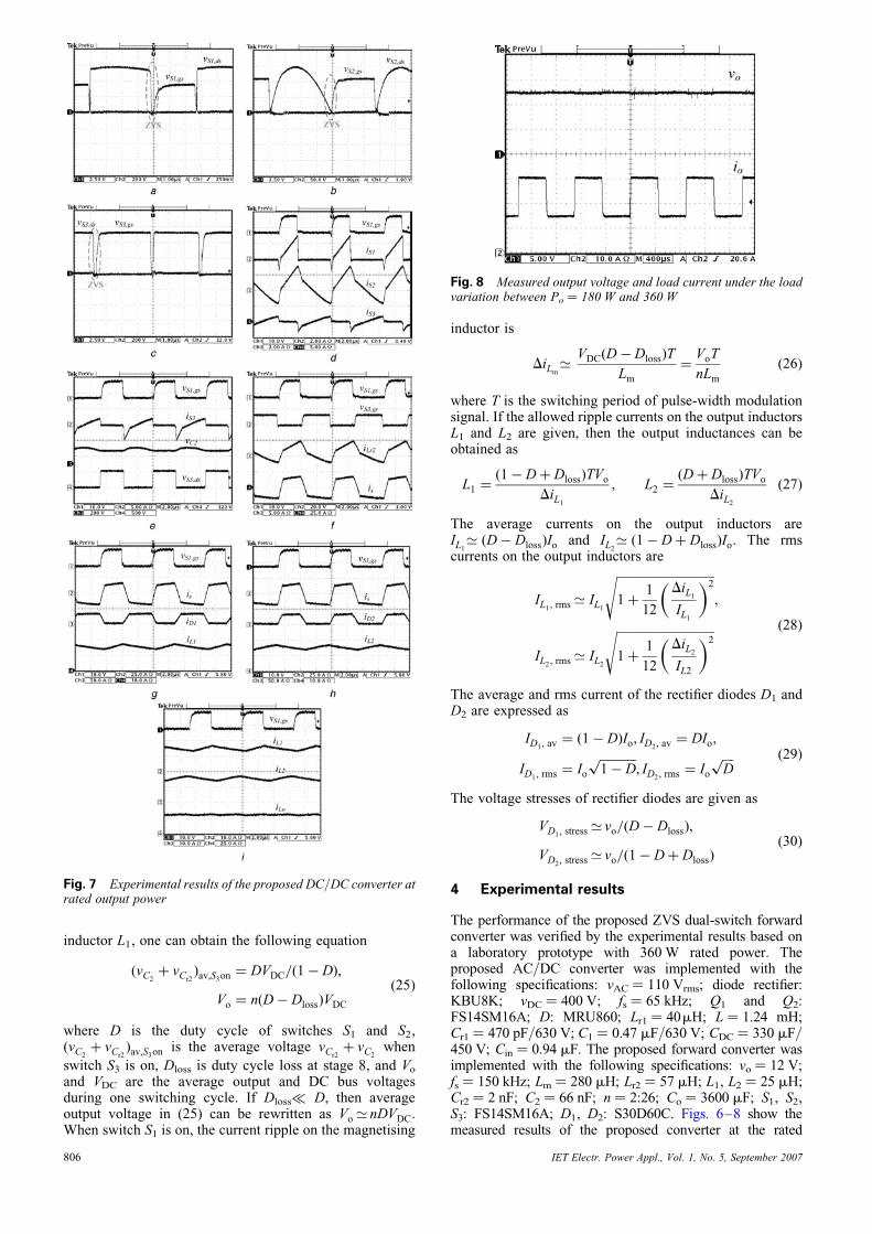
Fig. 8 Measured output voltage and load current under the loadvariation between Po ¼ 180 W and 360 W
IET Electr. Power Appl., Vol. 1, No. 5, September 2007

power. The measured waveforms of the proposed AC/DCconverter are given in Fig. 6. Fig. 6a illustrates the measuredAC source voltage and line current. The line current iAC is asinusoidal waveform in phase with line voltage vAC. Themeasured power factor is 0.99 and the measured total harmo-nic distortion of line current is 6.38%. The measured gate anddrain voltages of switches Q1 and Q2 are shown in Fig. 6b.From the measured results, it is clear that the drain voltagesvQ1,ds and vQ2,ds have been decreased to zero before switchesQ1 and Q2 are turned on. Therefore both switches are turnedon at ZVS. Fig. 6c shows the measured gate voltages vQ1,gs
and vQ2,gs and switch currents iQ1and iQ2
. Both switches areturned on when switch currents are negative. It means thatthe anti-parallel diode of switch is on before the switch isturned on. Therefore the ZVS conditions for both switchesare achieved. The measured gate voltage vQ1,gs, input inductorcurrent iL, resonant inductor current iLr1 and diode current iDare given in Fig. 6d. When switchQ1 is turned on, the diodeDis turned off and the input inductor current iL equals theresonant inductor current iLr1 . When switch Q1 is turned off,the diode D is turned on and the input inductor currentiL ¼ iLr1 þ iD. Fig. 6e gives the measured gate voltagevQ1,gs, resonant inductor current iLr1 and switch currents iQ1
and iQ2. When Q1 is turned on and Q2 is turned off, the
switch current iQ2¼ 0 and the resonant inductor current
iLr1 ¼ iQ1. When Q1 is turned off and Q2 is turned on, the
switch current iQ1¼ 0 and the resonant inductor current
iLr1 ¼ �iQ2.
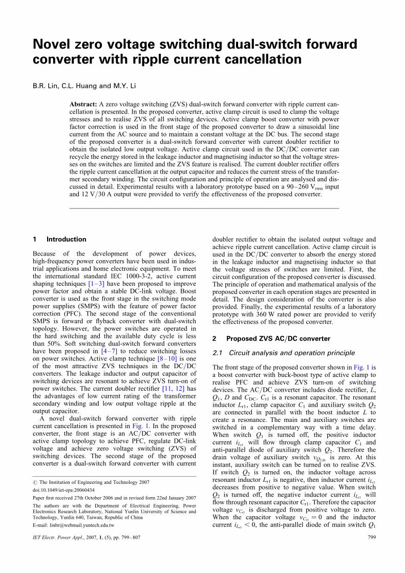
The measured results of the proposed forward converter atthe rated output power are shown in Fig. 7. Fig. 7a illustratesthe measured gate and drain voltages of switch S1. Beforeswitch S1 is turned on, the drain voltage vS1,ds has beendecreased to zero. Therefore the ZVS condition of switchS1 is achieved. Figs. 7b and 7c show the gate and drain vol-tages of switches S2 and S3. When switch S2 is turned off, thecapacitor Cr2 connected in parallel with switch S2 is resonantwith the inductor Lr2. The drain voltages vS2,ds and vS3,ds aredecreasing to zero before the gate voltages vS2,gs and vS3,gs arepositive. Therefore the ZVS conditions for switches S2 and S3are achieved. Fig. 7d illustrates the measured gate voltagevS1,gs and switch currents iS1 , iS2 and iS3 . When S1 is tunedon and S3 is turned off, the switch current iS3 ¼ 0 andiS1 ¼ iS2 ¼ iLr2 . When S1 is turned off and S3 is turnedon, the primary current iLr2 ¼ iS2 ¼ �iS3 and iS1 ¼ 0.Fig. 7e shows the measured gate voltage vS1,gs, switchcurrent iS3 , clamp voltage vC2
and drain voltage vS3, ds.When S1 is tuned on and S3 is tuned off, the switch currentiS3 ¼ 0 and vS3, ds ¼ vDC þ vC2
. When S1 is turned off andS3 is tuned on, the drain voltage vS3, ds ¼ 0. The clampcapacitor vC2
, resonant capacitor vCr2, magnetising inductor
Lm and resonant inductor Lr2 are resonant. Fig. 7f gives themeasured gate voltages vS1,gs and vS3, gs, primary current iLr2and secondary current is. The primary current iLr2 and second-ary current is increase when S1 is tuned on and S3 is tuned off.The primary current iLr2 and secondary current is decreasewhen S1 is tuned off and S3 is tuned on. Fig. 7g shows themeasured gate voltage vS1, gs, secondary current is, diodecurrent iD1
and output inductor current iL1 . When S1 is on,the secondary current is increases, diode current iD1
equalszero, and output inductor current iL1 increases. When S1 isoff, the secondary current is decreases, diode current iD1
equals load current and output inductor current iL1 decreases.Fig. 7h illustrates the measured gate voltage vS1,gs, the sec-ondary current is, diode current iD
2and output inductor
current iL2. When S1 is on, the secondary current is increases,
diode current iD2equals load current and output inductor
current iL2decreases. When S1 is off, the secondary current
is decreases, diode current iD2equals zero and output inductor
IET Electr. Power Appl., Vol. 1, No. 5, September 2007
current iL2 increases. Fig. 7i gives the measured gate voltagevS1,gs, output inductor currents iL1 and iL1 , and output currentiLo . The output current iLo ¼ iL1 þ iL2 . It is clear that theripple currents on the output inductors L1 and L2 are partiallycancelled each other in the output current iLO . The measuredoutput voltage and load current under the load variationbetween Po ¼ 180 W and 360 W are shown in Fig. 8. It isclear that the output voltage of the proposed converter isless sensitive to the load variation. The measured efficiencyof the proposed converter at the rated output power is 88.3%.
5 Conclusion
This paper presents a ZVS dual-switch forward converterwith current ripple cancellation. In the front stage of theproposed converter, active clamp boost converter withPFC is proposed to draw a sinusoidal line current fromthe AC source and to regulate the DC-link voltage. In theproposed DC/DC converter, active clamp circuit is usedin the dual-switch forward converter to realise transformerflux reset and achieve ZVS operation of all switchingdevices. The current doubler rectifier is used in the outputside to achieve ripple current cancellation on the outputcapacitor. The advantages of the proposed converter areallowed wide input voltage range, low voltage stress ofswitching devices and low current rating of the secondarywinding of transformer. Finally, the performance of the pro-posed converter is verified from the experimental resultsbased on a laboratory prototype. The experimental wave-forms agree with those predicted theoretically.
6 References
1 Duarte, C.M.C., and Barbi, I.: ‘A new ZVS-PWM active-clampinghigh power factor rectifier analysis, design, and experimentation’.Proc. of IEEE APEC,1998, pp. 230–236
2 Duarte, C.M.C., and Barbi, I.: ‘New family of ZVS-PWMactive-clamping DC-to-DC boost converters: analysis, design, andexperimentation’, IEEE Trans. Power Electron., 1997, 12, (5),pp. 824–831
3 Martinez, R., and Enjeti, P.N.: ‘A high-performance single-phaserectifier with input power factor correction’, IEEE Trans. PowerElectron., 1996, 11, (4), pp. 311–317
4 Moisseev, S., Hamada, S., and Nakaoka, M.: ‘Double two-switchforward transformer linked soft-switching PWM DC-DC powerconverter using IGBTs’, IEE Proc. Electr. Power Appl., 2003, 150,(1), pp. 31–38
5 Jang, Y., Dillman, D.L., and Jovanovic, M.M.: ‘Soft-switched PFCboost rectifier with integrated ZVS two-switch forward converter’.IEEE Conf. Rec. of IEEE Applied Power Electronics Conf. andExposition, APEC, 2005, vol. 2, pp. 1139–1144
6 Tofoli, F.L., Gallo, C.A., Coelho, E.A.A., de Freitas, L.C., Farias,V.J., and Vieira, J.B. Jr.: ‘A switched-mode power supplyemploying a quadratic boost converter and a soft-switchedtwo-switch forward converter’. IEEE Conf. Rec. of PowerElectronics Specialists Conf., PESC, 2004, vol. 4, pp. 2611–2614
7 Hamada, S., Moisseev, S., and Nakaoka, M.: ‘Two-switch forwardsoft-switching PWM DC-DC power converter’, IEE Electron. Lett.,2000, 36, (5), pp. 2055–2056
8 Li, Q.M., and Lee, F.C.: ‘Design consideration of the active-clampforward converter with current mode control during large-signaltransient’, IEEE Trans. Power Electron., 2003, 18, (4), pp. 958–965
9 Torrico-Bascop,R., andBarbi, I.: ‘A doubleZVS-PWMactive-clampingforward converter: analysis, design, and experimentation’, IEEE Trans.Power Electron., 2001, 16, (6), pp. 745–751
10 Lin, B.-R., Huang, C.E., and Wang, D.: ‘Analysis and implementationof a zero-voltage switching forward converter with a synchronousrectifier’, IEE Proc. Electr. Power Appl., 2005, 152, (5),pp. 1085–1092
11 Panov, Y., and Jovanovic, M.M.: ‘Design and performance evaluationof low-voltage/high-current dc/dc on-board modules’, IEEE Trans.Power Electron., 2001, 16, (1), pp. 26–33
12 Jian, S., Webb, K.F., and Mehrotra, V.: ‘Integrated magnetics forcurrent-doubler rectifiers’, IEEE Trans. Power Electron., 2004, 19,(3), pp. 582–590
807