novel materials and integration technologies for …
TRANSCRIPT

NOVEL MATERIALS AND INTEGRATION
TECHNOLOGIES FOR SILICON PHOTONICS
Dries Van Thourhout / September 2020

PHOTONICS RESEARCH GROUP
Research Group of Ghent University
— Faculty of Engineering and Architecture
— Department of Information Technology (INTEC)
— Associated laboratory of IMEC
— Member of the Center for Nano- & Biophotonics (NB photonics)
Technology Research
— Photonic Integration: Systems on a chip
— On silicon: “Silicon Photonics”
— Enhanced with new materials:III-V, ferro-electrics, graphene, …
Applications
— High-speed telecom and datacom
— Sensing for life sciences: visible and Mid-IR
— Optical information processing
9 Professors
16 postdocs
50 PhD students
10 support staff
20+ nationalities
6 ERC grants
6 spin-off companies
50 journal papers/year
Class 100 clean rooms
M.Sc. Photonics program

PROFESSORS
GROUP
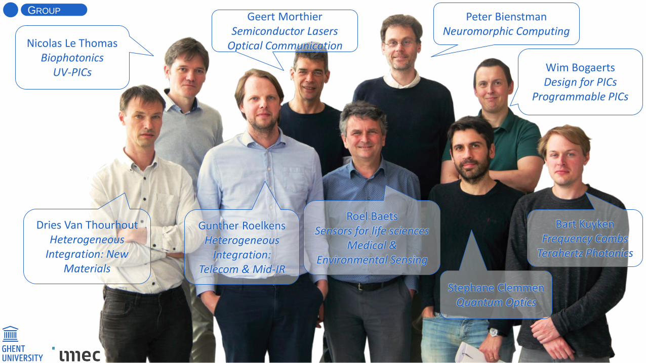
Nicolas Le ThomasBiophotonics
UV-PICs
Dries Van ThourhoutHeterogeneous
Integration: New Materials
Geert MorthierSemiconductor Lasers
Optical Communication
Peter BienstmanNeuromorphic Computing
Wim BogaertsDesign for PICs
Programmable PICs
Roel BaetsSensors for life sciences
Medical & Environmental Sensing
Gunther RoelkensHeterogeneous
Integration: Telecom & Mid-IR
Stephane ClemmenQuantum Optics
Bart KuykenFrequency Combs
Terahertz Photonics
GROUP

COMMON THEME: SILICON PHOTONICS?
The implementation of high density photonic integrated circuits by
means of CMOS process technology in a CMOS fab
Enabling complex optical functionality on a compact chip at low costPictures, courtesy of imec

SILICON PHOTONICS: OUR WAVEGUIDE(S)
… without leaving the CMOS fab
Si
SiO2
[2um box]
1.0 3.0 10.0 λ[um]
Ge
Si
Si3N4
SiO2
0.3
Al2O3
SiO2

IMEC SILICON-ON-INSULATOR PLATFORM
Co-integration of the various building blocks in a single platform
Today available on 200mm wafer size, coming soon on 300mm
95% compatible with CMOS130 in commercial foundries
Fully Integrated 8x56G DWDM Si Photonics Technology
56G Ge Electro-Absorption Modulator
56Gb/s eye diagram
56G Silicon Ring Modulator
56Gb/s eye diagram
8+1-channel DWDM (De-)Multiplexing Filter In-Plane Coupler
Surface-Normal Coupler
50G Ge Photodetector 50Gb/s eye diagram
56G Silicon Mach-Zehnder Modulator

NEED FOR NOVEL MATERIALS
Silicon is great but:
—Indirect bandgap: no efficient light emission
—Cubic lattice: no second order non-linearities, no electro-optic effect
Hence need for integration with new materials:
—Ferroelectrics (PZT, BTO) for phase modulators and SHG
—Graphene and other 2D-materials for intensity and phase modulators
—Colloidal quantum dots for light sources and single photon emitters
—Direct bandgap III-V semiconductors for efficient light emission

FERRO-ELECTRIC MATERIALS ON SILICON
More information: George, J. P., et al. ACS applied materials & interfaces (2015)
Lanthanide buffer layer
(10-20 nm)
PZT sol-gel deposition
(@ 500-600°C)
Developed new process to deposit BTO, LN, PZT on any substrate
PZT
SiN waveguide

ELECTRO-OPTIC MATERIALS ON SILICON
RESEARCH
PZT by spin coating
K. Alexander, Nature Communciations 2018
Collaboration J. Beeckman (LCP, UGent)

2D MATERIALS ON SILICON
Demonstrated high-speed graphene EA-modulators
Demonstrated single-photon emission from WSe2 coupled to SiN-WG
Exploration of novel 2D-materials for phase modulation
RESEARCH
C. Allessandri e.a. , Applied Optics 2019 F. Peyskens e.a. , Nature Comm. 2019

COLLOIDAL QUANTUM DOTS
Alternative gain material (mostly in visible)
Also: explored single photon emission properties, integration with SNPD
RESEARCH
Y. Zhu, ACS Photonics, 2017L. Elsinger, Nanoletters 2019
DFB-laser from SiN/QD/SiN stack PbS QD in plasmon antenna, PCG, SNPD
Collaboration Z. Hens, P. Geiregat (PCN, UGent)

III-V LASERS
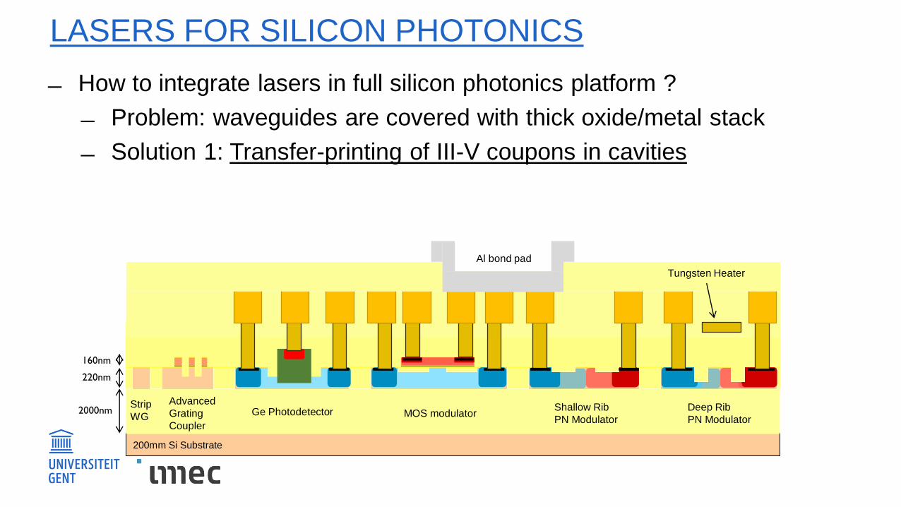
LASERS FOR SILICON PHOTONICS
How to integrate lasers in full silicon photonics platform ?
Problem: waveguides are covered with thick oxide/metal stack
Solution 1: Transfer-printing of III-V coupons in cavities
200mm Si Substrate
Advanced
Grating
Coupler
Ge Photodetector MOS modulatorShallow Rib
PN Modulator
Strip
WGDeep Rib
PN Modulator
Tungsten Heater
Al bond pad
220nm
160nm
2000nm

LASERS FOR SILICON PHOTONICS
200mm Si Substrate
Advanced
Grating
Coupler
MOS modulatorShallow Rib
PN Modulator
Strip
WGDeep Rib
PN Modulator
Tungsten Heater
Al bond pad
220nm
160nm
2000nm
< 100mm
How to integrate lasers in full silicon photonics platform ?
Problem: waveguides are covered with thick oxide/metal stack
Solution 1: Transfer-printing of III-V coupons in cavities

WHAT IS TRANSFER PRINTING ?PDMS Stamp
Source Substrate
Fast (>10 cm/s)
Devices picked Target substrate
Slow (<1 mm/s)
Devices attach
[M.Meitl et al., Nat. Mat 2005]
Approach:
III-V dies partly processed on source
wafer
Transfer on target SPh-wafer using
PDMS-stamp
Transfer printing promises:
Collective postprocessing on target wafer
Possibility for parallel transfer of multiple dies
and area magnification
No substrate removal needed (recycling of
wafers, less waste)

TRANSFER PRINTING
Enabling technology for heterogeneous integration on silicon photonics
Transfer of micro-scale III-V coupons/devices to a Si target wafer
InP, GaAs, GaSb, SOI, thin films,2D materials, 0D materials
RESEARCH

MICRO-TRANSFER-PRINTING (mTP)
Alignment accuracy promised by vendor: < 1 mm – 3 s
20
PROCESS CARRIED OUT USING COMMERCIAL TOOL FROM X-CELEPRINT
Lab-scale tool at Photonics Research Group (Ghent) Scalable to 300mm and panels

III-V-ON-SI WIDELY TUNABLE LASER WITH mTP
[J. Zhang et al., IEEE ECOC, 2019]
Prof. G. Roelkens & team

22
INTEGRATION OF AMPLIFIERS AND LASERS ON SILICON NITRIDE— Why: low loss, broader wavelength range
— Non-trivial given large index mismatch between InP and SiN
— Solution: intermediate amorphous silicon layer layer
Prof. B. Kuyken & team

23
INTEGRATION OF AMPLIFIERS AND LASERS ON SILICON NITRIDE
C. Op de Beeck, Optica 2020
On-chip Gain
Ring-Laser

24
500 um
250 umPRINTING ARRAYS OF PDS
Source pitchX = 100 um.Y = 125 um.
Stamp pitch (2x2)X = 500 umY = 250 um.
Target pitch: X = 500 umY = 250 um.Source wafer : After printing
Source wafer : before printing
Red – bad devices (2x2 printing skipped)
(4 devices failed)
Blue – devices printed 1x1 stamp.
500 um
250 um
Target wafer : After printing

LASERS FOR SILICON PHOTONICS
200mm Si Substrate
Advanced
Grating
Coupler
MOS modulatorShallow Rib
PN Modulator
Strip
WGDeep Rib
PN Modulator
Tungsten Heater
Al bond pad
220nm
160nm
2000nm
How to integrate lasers in full silicon photonics platform ?
Problem: waveguides are covered with thick oxide/metal stack
Solution 2: Direct epitaxial growth (III-V on silicon)

HETEROEPITAXY- CHALLENGES
III-V
SI
Lattice mismatch
MISFIT
Threading dislocation
LATTICE MISMATCH RESULTS IN UNWANTED DEFECTS

PROPOSED PROCESS: ASPECT RATIO TRAPPING
27
a) Etching ridges in silicon
Si
b) Planarization
SiO2
c) KOH-etch silicon
d) Nucleation and growth in trenches
e) Further growth out of trenches
Developed by B. Kunert e.a., imec
Reference sample

ASPECT RATIO TRAPPING (ART)
High-AR SiO2 trenches enable trapping of threading dislocations
SiO2
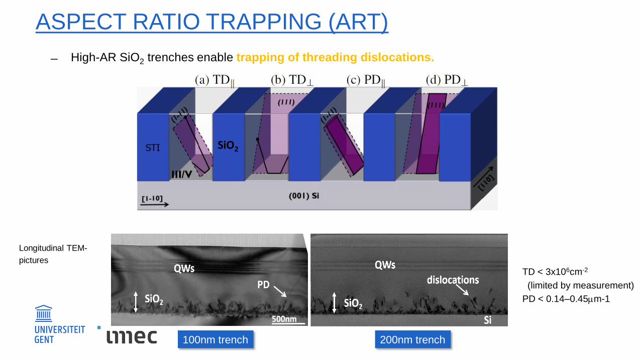
ASPECT RATIO TRAPPING (ART)
High-AR SiO2 trenches enable trapping of threading dislocations.
100nm trench 200nm trench
SiO2
Longitudinal TEM-
pictures
TD < 3x106cm-2
(limited by measurement)
PD < 0.14–0.45mm-1

NANO-RIDGE ENGINEERING (NRE)
Control growth rate on different crystal planes to obtain well-defined nano-ridge profileHigher growth rate facets disappear, whereas facets with lower growth rates define the nano-ridge profile

31
TRANSVERSAL OPTICAL MODES IN NANO-RIDGE WITH 100NM-TRENCH WIDTH
1mM-WAVELENGTH NANO-RIDGE LASER
TE-LIKE GROUND MODES IN NANO-RIDGES
Y. Shi, OPTICA, 4(12), p.1468-1473 (2017)

MEASURED SPECTRUM LIGHT-IN LIGHT OUT
SPECTRA FOR NANO-RIDGES
WITH DIFFERENT TRENCH WAVELENGTH TUNING
l/4-SHIFT INDEX COUPLED DFB LASER
Y. Shi, Optica, 4(12), p.1468-1473 (2017)
Etched Grating

EBH
EBL
n
Bloch modes: EBH (high overlap) ELH (low overlap)
Loss: 𝛼EBH≈ 10 × 𝛼EBL
Continuous Au-contact: 𝛼𝑇𝐸 = 74 𝑐𝑚-1
Grating with 40% duty cycle: 𝛼EBL= 7𝑐𝑚-1
METAL GRATING ON NANO-RIDGE
DFB-LASER WITH METAL GRATING

DFB-LASER WITH METAL GRATING
MEASURED SPECTRUM LIGHT-IN LIGHT OUT THRESHOLD/POWER VS DUTY CYCLE
Trade-off between coupling factor and loss results in optimal duty cycle of 40%

35
COUPLING LIGHT TO SILICON WAVEGUIDE
PROPOSED CONFIGURATION PHASE MATCH CONDITIONCROSS SECTION
POWER EXCHANGE COUPLING IN O-BAND

36
IMPROVED VERSION
PROPOSED CONFIGURATION TOP VIEW
POWER EXCHANGE POWER EXCHANGE
L=310mm
Standalone WG mode Supermode

37
FURTHER IMPROVED VERSION
Hsien-kai Hsiao, et al. Midinfrared broadband achromatic astronomical beam combiner for nulling interferometry. Applied optics, 49(35):6675–6688, 2010.
PROPOSED CONFIGURATION TOP VIEW
POWER EXCHANGE
BLACKMAN FUNCTION
Y. Shi, Optics Express 27(26), p.37781-37794 (2019)

OUTLOOK (EPITAXY)
Electrical injection ?
Micro-lasers ?
Single Photon Emission ?NARIOS
current in
current out

SUMMARY

SUMMARY & CONCLUSIONS
Novel materials clearly show prospects for performance beyond what is
currently available in existing platforms
LN, BTO, PZT high-speed modulators demonstrated by several
groups and now in ”spin-off” phase
Graphene devices heavily investigated in Graphene Flagship
III-V integration through transfer printing and EPI rapidly evolving
But still a lot of room (and need) for further improvement and research
On fundamental building blocks and even materials
Towards new applications enabled by these building blocks

ACKNOWLEDGEMENTS
UGent Photonics Research Group
IMEC OIO & EPI teams (J. Van Campenhout, M. Pantouvaki, B. Kunert)
UGent PCN (Z. Hens, P. Geiregat)
UGent LCP (J. Beeckman)
Funding
BOF UGent, FWO, EU Commission (ERC, Graphene Flagship,
Teraboard, Caladan…)
41

Ghent University
@DThourhout
Ghent University
Prof. Dries Van ThourhoutPHOTONICS RESEARCH GROUP
T +32 9 264 34 38
www.photonics.intec.ugent.be