novel iii-nitride semiconductors for solar hydrogen productionetheses.whiterose.ac.uk/7644/1/j...
TRANSCRIPT

Novel III-Nitride Semiconductors for Solar
Hydrogen Production
Jonathan Benton
The University of Sheffield
Department of Electronic and Electrical Engineering
Department of Chemistry
III-V Nitrides Group
Supervisors: Professor Tao Wang and Dr Julia Weinstein
A Thesis submitted for the degree of Doctor of Philosophy


i
Abstract
III-nitride materials are crucially becoming the most important and
promising class of semiconductors for future optoelectronic devices
including solid state lighting and solar energy applications. Presently, there
are still many challenges in regards to the wide scale uptake of these devices,
including low efficiencies and short lifetimes. Despite the ideal properties of
InGaN for water splitting, there are still very few reports utilising these
semiconductors.
This thesis investigates GaN and InGaN based structures for water
splitting. Initially focussing on the fabrication of nanorods via the use of a self-
organised nickel mask, where diameter and height of the structures have
been optimised. As a result, the surface area of the device increases
dramatically leading to an enhancement in photocurrent compared to as-
grown planar devices. Alongside this, the fabricated nanostructures allow for
an enhancement in electron-hole separation and an increase in the hydrogen
generation rate.
The lifetime of the fabricated devices is also discussed. Prolonged
exposure of the nanostructured devices results in the degradation and
etching of the InGaN material. The addition of a secondary semiconductor
material, NiO, acts as a reaction site for photogenerated holes preventing the
oxidation and dissolution of InGaN devices in the experimental electrolytes,
increasing the device lifetime.
Furthermore, a photoelectrochemical etch technique is implemented
to create a porous device structure. The nanoporous network in the
structure shortens the required diffusion length of the photogenerated
carriers to values close to that of InGaN. An enhancement in photocurrent
and hydrogen production has been observed due to the nanoporous
structure.

ii

iii
Acknowledgements
I am grateful to a number of people who have provided their support
and wisdom throughout the course of this thesis. Firstly my supervisor
Professor Tao Wang has been invaluable in his guidance and his expertise.
The faith he has had in me personally and the opportunities that I have
obtained while under his supervision has helped to shape me into the person
I have become. My thanks are also extended to my second supervisor Doctor
Julia Weinstein for her interest and encouragement in the progress of my
research.
The members of the Sheffield Nitride group both past and present
have provided me both with their insights and friendship. My initial thanks go
to Doctor Qi Wang and Doctor Jie Bai who trained me in device
characterisation and fabrication, effectively allowing this thesis to be possible.
Doctor Yipin Gong, Kun Xing, Xiang Yu and Benbo Xu grew samples for this
work and performed growth characterisation. Doctor Paul Renwick, Doctor
Rick Smith and Modestos Athanasiou have been invaluable office companions
providing discussion across a range of subjects, aiding in the development of
this work as well as creating an enjoyable working environment. The
technical support of Paul Haines and the other members of the technical
team have allowed a minimum level of disruption through their skill in the
maintenance of equipment.
My friends and family have been a great support over the past 4 years,
keeping me motivated and focused. A particular mention goes to my partner
Matt without whom life would be a very boring place.
Thank you all for sticking with me in my pursuits.

iv

v
Publication List
(1) J. Benton, J. Bai & T. Wang
"Utilisation of GaN and InGaN/GaN with Nanoporous Structures for Water
Splitting”
Applied Physics Letters, 105, 223902 (2014)
(2) J. Benton, J. Bai & T. Wang
"Nanoporous GaN for enhanced solar hydrogen production"
Solar Hydrogen and Nanotechnology IX, SPIE Proceedings, 91760K, (2014)
(3) J. Benton, J. Bai & T. Wang
"Significantly enhanced performance of an InGaN/GaN nanostructure based
photo-electrode for solar power hydrogen generation"
Applied Physics Letters, 103, 133904 (2013)
(4) J. Benton, J. Bai & T. Wang
"Enhancement in hydrogen generation efficiency using a GaN nanostructure"
Applied Physics Letters, 102, 173905, (2013)
(5) J. Benton, J. Bai & T. Wang
"Nanoporous GaN for enhanced solar hydrogen production"
Solar Hydrogen and Nanotechnology IX, SPIE Optics & Photonics 2014, San
Diego, United States, 17th – 21st August 2014 – Oral presentation
(6) J. Benton, J. Bai & T. Wang
"Porous GaN for solar hydrogen production"
UKNC Bristol 2014, Bristol, United Kingdom, 7-8th January 2014 – Oral
presentation

vi
(7) J. Benton, J. Bai & T. Wang
"Reduced photoelectrochemical etching of GaN/InGaN structure for solar
hydrogen production"
UKNC Sheffield 2013, Sheffield, United Kingdom, 4th July 2013 – Oral
presentation
(8) J. Benton, J. Bai & T. Wang
"Enhancement in hydrogen generation efficiency using GaN nanostructure",
7th International Workshop on Nitride Semi-Conductors, Sapporo, Japan, 14-
19th October 2012 – Oral presentation
(9) J. Benton, J. Bai & T. Wang
"Photoelectrochemical reaction & hydrogen production of n-type GaN"
UKNC Sheffield 2012, Sheffield, United Kingdom, 5th July 2012 – Oral
presentation

vii
Contents
NOVEL III-NITRIDE SEMICONDUCTORS FOR SOLAR HYDROGEN
PRODUCTION 1
ABSTRACT I
ACKNOWLEDGEMENTS III
PUBLICATION LIST V
CONTENTS VII
LIST OF FIGURES XI
LIST OF TABLES XVII
INTRODUCTION - 1 -
1.1 A HISTORICAL PERSPECTIVE - 1 -
1.2 CLIMATE CHANGE & HYDROGEN - 2 -
1.2.1 Solar Hydrogen - 6 -
Photoelectrochemical Hydrogen - 7 -
1.3 ISSUES & LIMITATIONS - 8 -
1.4 III-NITRIDES - 9 -
BIBLIOGRAPHY - 13 -
BACKGROUND - 19 -
2.1 SEMICONDUCTORS - 19 -
2.1.1 Conduction, Mobility and Recombination - 22 -
2.1.3 Optical Properties - 24 -
2.1.4 Semiconductor-Metal Interface - 25 -
2.2 III-NITRIDE SEMICONDUCTORS - 26 -
2.2.1 Structural Properties - 27 -
2.2.2 Band Gaps - 28 -
2.2.3 Growth - 28 -
Doping - 30 -
2.2.4 III-nitride Devices - 31 -
Quantum Wells - 31 -
Ohmic Contacts - 34 -
2.3 ELECTROCHEMISTRY - 34 -
2.3.2 Mass & Charge Transport - 37 -
Electric Double Layer - 39 -
2.3.3 Semiconductor-Electrolyte Interface - 41 -
Electron-Transfer Reactions - 43 -
2.4 PHOTOELECTROLYSIS - 44 -
2.4.1 Efficiencies - 48 -
2.4.2 Current Approaches - 49 -
Photocorrosion - 51 -
viii
2.4.4 III-Nitrides in Water Splitting - 52 -
BIBLIOGRAPHY - 55 -
EXPERIMENTAL TECHNIQUES - 63 -
3.1 GROWTH - 63 -
3.2 FABRICATION - 64 -
3.2.1 Dry Etch Techniques - 64 -
Reactive-Ion Etching - 65 -
Inductively Coupled Plasma RIE - 66 -
3.2.2 Photolithography - 66 -
3.2.3 Thin Film Deposition - 67 -
Plasma Enhanced Chemical Vapour Deposition - 67 -
Thermal Evaporation - 68 -
E-beam Evaporation - 69 -
Sputter Deposition - 69 -
3.2.5 Rapid Thermal Annealing - 69 -
3.3 CHARACTERISATION - 70 -
3.3.1 Photoluminescence - 70 -
3.3.2 Scanning Electron Microscopy - 71 -
3.3.3 Atomic Force Microscopy - 71 -
3.4 PHOTOELECTROCHEMICAL TECHNIQUES - 72 -
3.4.1 PEC Cell - 72 -
3.4.2 Step Voltage Testing - 73 -
3.4.3 Reliability Testing - 74 -
Hydrogen Monitoring - 74 -
3.4.4 Incident Photon Conversion Efficiency - 74 -
3.4.5 Accuracy and Error - 75 -
BIBLIOGRAPHY - 76 -
GAN NANOSTRUCTURES FOR ENHANCED SOLAR HYDROGEN
PRODUCTION - 77 -
4.1 BACKGROUND - 77 -
4.1.1 Nanostructures for Solar Hydrogen - 77 -
4.1.2 GaN Nanorods - 79 -
GaN Nanostructures in Water Splitting - 80 -
4.2 AS-GROWN GAN DEVICES - 80 -
4.2.1 Fabrication - 80 -
4.2.2 Device Characterisation - 81 -
Atomic Force Microscopy (AFM) - 82 -
Hall Measurements - 83 -
4.2.3 Solar Hydrogen Performance - 84 -
Preliminary Measurements - 84 -
Electrolytes - 87 -
4.2.4 Summary - 89 -
4.3 GAN NANOSTRUCTURED DEVICES - 89 -

ix
4.3.1 Fabrication - 89 -
4.3.2 Characterisation of Nanostructures - 91 -
Nanorod Diameter - 92 -
Nanorod Height - 95 -
4.3.3 Solar Hydrogen Performance - 95 -
Nanorod Diameter - 96 -
Height Optimisation - 97 -
4.3.4 Summary - 99 -
4.4 INGAN/GAN IN WATER SPLITTING - 99 -
4.4.1 Fabrication of InGaN/GaN MQW Devices - 99 -
4.4.2 Characterisation - 100 -
4.4.3 Solar Hydrogen Performance - 101 -
4.4.4 Summary - 104 -
4.5 CONCLUSIONS - 104 -
BIBLIOGRAPHY - 105 -
NIO NANOPARTICLES ON GAN NANORODS FOR REDUCED ETCHING - 109 -
5.1 COCATALYSTS IN WATER SPLITTING - 109 -
5.1.1 Cocatalysts on GaN - 112 -
5.2 GAN/INGAN DEVICES - 112 -
5.2.1 Fabrication - 113 -
5.2.2 Characterisation - 115 -
5.2.3 Step Photocurrent Measurements - 117 -
5.2.4 Steady State Measurements - 119 -
5.3 CONCLUSIONS - 126 -
BIBLIOGRAPHY - 127 -
NANOPOROUS GAN FOR ENHANCED PHOTOELECTROCHEMICAL
ACTIVITY - 129 -
6.1 POROUS SEMICONDUCTORS IN WATER SPLITTING - 129 -
6.2 HISTORY OF POROUS GAN & INGAN - 130 -
6.2.1 Etching Process - 132 -
6.2.2 Etched GaN/InGaN in Water Splitting - 133 -
6.3 NANOPOROUS GAN - 134 -
6.3.1 Fabrication - 134 -
Planar Porous GaN - 134 -
Porous Nanostructure GaN - 135 -
6.3.2 Characterisation - 136 -
Photoluminescence - 136 -
SEM Measurements - 139 -
6.3.3 Solar Hydrogen Performance - 143 -
Hydrogen Generation - 146 -
Incident Photon Conversion Efficiency - 147 -
6.3.4 Summary - 148 -
6.4 NIO NANOPARTICLES ON NANOPOROUS GAN - 149 -
x
6.4.1 Fabrication - 149 -
6.4.2 Characterisation - 150 -
6.4.3 Solar Hydrogen Performance - 150 -
6.4.4 Summary - 151 -
6.5 NANOPOROUS INGAN/GAN MQW - 152 -
6.5.1 Fabrication - 152 -
6.5.2 Characterisation - 153 -
6.5.3 Solar Hydrogen Performance - 155 -
Hydrogen Measurements - 155 -
Incident Photon Conversion Efficiency - 156 -
6.5.4 Summary - 157 -
6.6 CONCLUSIONS - 157 -
BIBLIOGRAPHY - 159 -
CONCLUSION - 163 -
7.1 OVERVIEW - 163 -
7.2 FUTURE RESEARCH - 166 -
7.2.1 InGaN bulk films - 167 -
7.2.2 Intermediate Bands - 167 -
7.2.3 Device Properties - 168 -
7.2.4 Summary - 168 -
BIBLIOGRAPHY - 169 -

xi
List of Figures
FIGURE 1-1 – CHANGES IN GLOBAL POPULATION AND OIL PRODUCTION 1950-2010. POPULATION
DATA FROM WORLD POPULATION PROSPECTS, UNITED NATIONS DEPARTMENT OF
ECONOMIC AND SOCIAL AFFAIRS, 2011.8 OIL DATA FROM WORLD OIL PRODUCTION 1950-
2009, EARTH POLICY INSTITUTE, 2011. - 2 - FIGURE 1-2 – CHANGES IN WORLD PRIMARY ENERGY SUPPLY 1971-2010 IN KILO TONS OF OIL
EQUIVALENT. DATA SOURCE INTERNATIONAL ENERGY AGENCY (IEA) VIA UK DATA SERVICE
- 3 - FIGURE 1-3 – CHANGES IN TRANSPORT CO2 EMISSIONS FROM 1971 TO 2011 AS A PROPORTION OF
TOTAL GLOBAL CO2. DATA SOURCE INTERNATIONAL ENERGY AGENCY (IEA) VIA UK DATA
SERVICE - 4 - FIGURE 1-4 - BASIC SCHEMATIC OF PHOTOELECTROCHEMICAL CELL UNDER OPERATION - 7 - FIGURE 1-5 – NUMBER OF PUBLICATIONS (WEB OF KNOWLEDGE) AND DEVELOPMENT OF GAN
SINCE 1969 - 10 - FIGURE 1-6 - PLOT OF BAND GAP OF INXGA1-XN AT VARIOUS INDIUM COMPOSITIONS
74 ALONGSIDE
INTENSITY OF SOLAR ENERGY - 11 - FIGURE 2-1 – ILLUSTRATION OF METAL, SEMICONDUCTOR AND INSULATOR BAND STRUCTURES
- 20 - FIGURE 2-2 – REPRESENTATION OF DIRECT AND INDIRECT BAND STRUCTURES ON ENERGY-
MOMENTUM DIAGRAMS - 21 - FIGURE 2-4 – RADIATIVE RECOMBINATION MECHANISMS IN SEMICONDUCTORS
7 - 24 - FIGURE 2-5 – SCHEMATIC REPRESENTATION OF METAL-SEMICONDUCTOR (N-TYPE) BAND
STRUCTURES WHEN SEPARATED AND IN INTIMATE OHMIC CONTACT - 26 - FIGURE 2-6 – ATOMIC STRUCTURES OF DIFFERENT CRYSTAL STRUCTURES (A) ZINC BLENDE (B)
WURTZITE (C) ROCK SALT - 27 - FIGURE 2-7 – (A) SIMPLE MODEL OF OPTICAL ABSORPTION IN QUANTUM WELLS (B) DENSITY OF
STATES FOR A BULK (DASHED) AND QUANTUM WELL SEMICONDUCTOR - 32 - FIGURE 2-8 – EFFECT OF POLARIZATION ON QUANTUM WELL BAND DIAGRAMS (A) POLAR C-PLANE
GAN (B) NONPOLAR M-PLANE GAN44 - 33 - FIGURE 2-9 – ILLUSTRATION OF OXIDATION AND REDUCTION REACTIONS OCCURRING AT
ELECTRODE-ELECTROLYTE INTERFACE - 36 - FIGURE 2-10 – GENERAL REACTION PATHWAY AND MASS TRANSPORT BETWEEN BULK SOLUTION
AND SURFACE REGION OF ELECTRODE. ADAPTED FROM BARD & FAULKNER, 2001.55 - 38 - FIGURE 2-11 – REPRESENTATION OF DIFFERENT DOUBLE LAYER MODELS PLUS ELECTROSTATIC
POTENTIAL (Φ) DIAGRAMS VERSUS DISTANCE FROM ELECTRODE (X) OF EACH MODEL (A)
HELMHOLTZ (B) GOUY-CHAPMAN (C) STERN MODELS - 40 - FIGURE 2-12 – BAND STRUCTURES OF N-TYPE SEMICONDUCTORS IN ELECTROLYTE SOLUTION (A)
EQUIVALENT FERMI LEVEL AND REDOX POTENTIALS (B) SEMICONDUCTOR FERMI LEVEL <
REDOX POTENTIAL (C) SEMICONDUCTOR FERMI LEVEL > REDOX POTENTIAL (D)
SEMICONDUCTOR FERMI LEVEL >> REDOX POTENTIAL - 42 - FIGURE 2-13 – ELECTRON-TRANSFER REACTIONS FOR N-TYPE SEMICONDUCTOR WITH REDOX
ELECTROLYTE (A) OVERLAP AT CONDUCTION BAND (B) VALENCE BAND OVERLAP (C)
CONJUGATION OF SURFACE STATES & REDOX LEVEL - 44 -

xii
FIGURE 2-14 – ENERGY DIAGRAMS OF WATER SPLITTING BASED ON (I) TYPE I SYSTEM USING A
SINGLE SEMICONDUCTOR AND EXCITATION AND (II) TYPE II IN WHICH A TWO-STEP
EXCITATION OF TWO SEMICONDUCTORS (Z-SCHEME) - 46 - FIGURE 2-15 – SCHEMATIC OF N-TYPE PHOTOANODE UNDER OPERATION FROM IRRADIATION
SOURCE - 47 - FIGURE 2-16 – BAND POSITIONS OF VARIOUS SEMICONDUCTORS UTILISED FOR SOLAR HYDROGEN
PRODUCTION - 50 - FIGURE 2-17 – TIMELINE OF DEVELOPMENTS IN III-NITRIDES FOR WATER SPLITTING. ONLY FIRST OR
SIGNIFICANT REPORTS MENTIONED AND LISTED IN PUBLICATION ORDER - 52 - FIGURE 3-1 – SCHEMATIC ILLUSTRATION OF REACTION PROCESS IN A METAL ORGANIC CHEMICAL
VAPOUR DEPOSITION (MOCVD) REACTOR FOR THE GROWTH OF GAN - 64 - FIGURE 3-2 – SCHEMATIC OF PHOTOLUMINESCENCE EXPERIMENTAL SET-UP - 70 - FIGURE 3-3 - PHOTOGRAPH OF PHOTOELECTROCHEMICAL CELL UTILISED IN MAJORITY OF TESTING
- 72 - FIGURE 3-4 - SCHEMATIC OF EXPERIMENTAL SET-UP - 73 - FIGURE 4-1 – VARIATION IN CHARGE COLLECTION IN DIFFERENT SEMICONDUCTOR STRUCTURES. LH:
HOLE DIFFUSION LENGTH; LE: ELECTRON DIFFUSION LENGTH. ADAPTED FROM OSTERLOH
(2013)2 - 78 - FIGURE 4-2 – ROOM TEMPERATURE PHOTOLUMINESCENCE OF SILICON DOPED GAN (INSET)
SCHEMATIC OF DONOR-ACCEPTOR RECOMBINATION MODEL IN N-GAN - 82 - FIGURE 4-3 – AFM SCAN OF N-TYPE GAN WAFER (A) 100 µM
2 SURFACE PROFILE (B) 3D
TOPOGRAPHY OF 4 µM2 SCAN - 83 -
FIGURE 4-4 - VARIATION IN CURRENT DENSITY WITH CARRIER CONCENTRATION OF DIFFERENT
SAMPLES AT 0 V BIAS IN 1 M HCL UNDER 150 W XE LAMP ILLUMINATION, BLACK SQUARES
INDICATE SAMPLES FROM SAME TEST RUN, RED CIRCLES ARE LITERATURE VALUES OF VARIOUS
TESTS. SHADED AREA INDICATES CARRIER CONCENTRATION OF DEVICES USED IN THIS WORK.
ADAPTED FROM ONO ET AL.. 200736 - 84 - FIGURE 4-5 – DARK AND LIGHT PHOTOCURRENT MEASUREMENTS OF AS-GROWN N- AND P-TYPE
GAN DEVICES IN A 1 M HCL ELECTROLYTE SOLUTION. ILLUMINATION INTENSTIY WAS 100
MW CM-2. - 85 - FIGURE 4-6 – PHOTOELECTROCHEMICAL WATER SPLITTING OF 0.5 M HCL WITH N-GAN
ELECTRODE UNDER ~500 MW CM-2
AND 0.8 V APPLIED BIAS (A) PHOTOCURRENT DENSITY
(B) THEORETICAL AND ACTUAL HYDROGEN PRODUCTION - 86 - FIGURE 4-7 – PHOTOCURRENT DENSITIES OF N-GAN WITH DIFFERENT ELECTROLYTES UNDER 100
MW CM-2
AM1.5 XE LAMP ILLUMINATION - 87 - FIGURE 4-8 – SCHEMATIC OF NANOROD FABRICATION VIA USE OF SELF-ORGANISED NICKEL
NANOPARTICLES - 90 - FIGURE 4-9 – SEM IMAGES OF NANOROD FABRICATION (A) NICKEL NANOISLAND MASK (B)
ETCHED SILICON DIOXIDE MASK (C) PLAN VIEW OF FABRICATED NANORODS (D) TILTED IMAGE
OF FINISHED NANORODS - 91 - FIGURE 4-10 – RELATIONSHIP BETWEEN NICKEL THICKNESS AND NANOROD DIAMETER (INSET)
VARIATION IN NANOROD DENSITY PER CM2 - 92 -
FIGURE 4-11 - DEVIATION OF NANOROD DIAMETERS WITH DIFFERENT NICKEL FILM THICKNESSES
- 93 - FIGURE 4-12 - SEM INDICATING NANOROD SIZE AND DENSITY OF VARIOUS NICKEL MASK
THICKNESSES (A) 4 NM (B) 6 NM (C) 8 NM (D) 10 NM (E) 15 NM (F) 20 NM - 94 -
xiii
FIGURE 4-13 - NORMALIZED ROOM TEMPERATURE PL OF DIFFERENT DIAMETER NANORODS - 95 - FIGURE 4-14 – (A) VARIATION OF NANOROD HEIGHT WITH ETCH TIME (B) SEM OF 1.5 MINUTE ICP
ETCH (C) SEM OF 10 MINUTE ICP ETCH - 95 - FIGURE 4-15 - PHOTOCURRENT VALUES FOR DIFFERENT NANOROD DIAMETERS CAUSED BY VARYING
NICKEL THICKNESS - 96 - FIGURE 4-16 – VARIATION IN ETCH DEPTH OF GAN NANORODS - 98 - FIGURE 4-17 – CHANGES IN ABSORBED FLUX OF DIFFERENT NANORODS (A) 150 NM NANORODS (B)
1000 NM NANORODS - 99 - FIGURE 4-18 – STRUCTURE OF INGAN/GAN MQW WAFER - 100 - FIGURE 4-19 – CHARACTERISATION OF INGAN/GAN MQW SAMPLES (A) NORMALISED ROOM
TEMPERATURE PL MEASUREMENTS OF AS-GROWN AND NANOROD DEVICES (B) SEM IMAGE
OF FABRICATED NANORODS - 101 - FIGURE 4-20 – PHOTOCURRENT OF AS-GROWN AND NANOROD PHOTOELECTRODES AS A
FUNCTION OF BIAS UNDER 100 MW CM-2
ILLUMINATION AND "DARK" CONDITIONS - 102 - FIGURE 4-21 – PHOTOELECTROCHEMICAL MEASUREMENTS UNDER 400 MW CM
-2 ILLUMINATION
AND 0.8 V BIAS (A) PHOTOCURRENTS OF THE AS-GROWN AND NANOROD SAMPLE AS A
FUNCTION OF TIME (B) OBTAINED AND THEORETICAL HYDROGEN MEASUREMENTS AS A
FUNCTION OF TIME - 103 - FIGURE 5-1 – ILLUSTRATION OF HYDROGEN AND OXYGEN EVOLUTION ON A CORE/SHELL
STRUCTURE ON A BULK PHOTOELECTRODE MATERIAL. ADAPTED FROM MAEDA, 2010.2 - 110 - FIGURE 5-2 - BAND STRUCTURES OF WIDE BAND GAP SEMICONDUCTOR (I) AND COCATALYST (II)
- 111 - FIGURE 5-3 – RELATIVE CONDUCTION AND VALENCE BAND POSITIONS OF NIO AND GAN BASED
SEMICONDUCTORS - 113 - FIGURE 5-4 – EXAMPLES OF NIO FABRICATION (A) AFTER NICKEL DEPOSITION (B) AFTER
ANNEALING - 114 - FIGURE 5-5 – SEM IMAGES OF INGAN/GAN MQW WITH AND WITHOUT NIO. INSETS DISPLAY
PLAN VIEW OF NANORODS. (A) FROM WAFER A (B) FROM WAFER A W/NIO (C) FROM WAFER
B (D) FROM WAFER B W/NIO (E) FROM WAFER C (F) FROM AFER C W/NIO - 115 - FIGURE 5-6 – ROOM TEMPERATURE PHOTOLUMINESCENCE OF INGAN/GAN MQW WAFERS WITH
AND WITHOUT NIO - 116 - FIGURE 5-7 – PHOTOCURRENT MEASUREMENTS AT 100 MW CM-2 IRRADIATION IN A 1 M NAOH
ELECTROLYTE AT BIASES FROM -1 TO 2 V (A) PLANAR N-TYPE GAN (B) INGAN/GAN NANO
STRUCTURE FROM WAFER A (C) INGAN/GAN NANOSTRUCTURE FROM WAFER B (D)
INGAN/GAN NANOSTRUCTURE FROM WAFER C - 118 - FIGURE 5-8 – SCHEMATIC OF THE BAND DIAGRAMS AND ILLUMINATION MECHANISM OCCURRING IN
GAN/NIO STRUCTURE WHEN NIO NANOARTICLES OR GAN ARE ILLUMINATED - 119 - FIGURE 5-9 – STEADY STATE PHOTOCURRENT MEASUREMENTS OF THE DEVICE FABRICATED FROM
WAFER B WITH AND WITHOUT NIO. PERFORMANCE ENHANCEMENT OVER THE DEVICE
WITHOUT NIO NANOPARTICLES AS A REFERENCE SAMPLE OVER TIME ALSO ILLUSTRATED.
- 120 - FIGURE 5-10 – SEM IMAGES OF NANORODS OVER TIME AFTER PHOTOCURRENT MEASUREMENTS.
LEFT HAND SIDE: REFERENCE NANORODS, RIGHT HAND SIDE: NANORODS WITH NIO (A)-(D)
DEVICES FROM WAFER B AT 15 MINUTES, 50 MINUTES, 105 MINUTES AND 180 MINUTES (E)
DEVICES FROM WAFER A AT 180 MINUTES (F) DEVICES FROM WAFER C AT 180 MINUTES
- 121 -

xiv
FIGURE 5-11 – ANALYSIS PROCESS WHEN USING IMAGEJ (A) INITIAL LOADING OF THE IMAGE (B)
BINARY CONVERSION OF THE IMAGE (C) DETAILED ANALYSIS OF EACH PARTICLE - 123 - FIGURE 5-12 – NANOROD COVERAGE OF ALL SIX DEVICES WITH AND WITHOUT NIO BASED ON
IMAGEJ ANALYSIS OF TOP-DOWN SEMS, REPRESENTATIVE ERRORS ARE ILLUSTRATED FOR
DEVICES FROM WAFER B - 124 - FIGURE 5-13 – DISTRIBUTION OF NANOROD SIZES FOR (A) WAFER B AND (B) WAFER B W/NIO
- 125 - FIGURE 6-1 - AFM IMAGE OF EARLY POROUS GAN LAYER, INSET IMAGE DISPLAYS AN ENLARGED
SINGLE PIT, GREYSCALE OF IMAGE CORRESPONDS TO HEIGHT VARIATION OF 150 NM. ADAPTED
FROM (MYNBAEVA, 2000)21 AND PERMISSION OBTAINED FROM COPYRIGHT HOLDER © AIP
PUBLISHING - 131 - FIGURE 6-2 – NORMALISED ROOM TEMPERATURE PL SPECTRA OF NANO POROUS STRUCTURES
FABRICATED FROM A PLANAR AS-GROWN WAFER - 137 - FIGURE 6-3 – ROOM TEMPERATURE PL FOR NANOPOROUS NANOROD SAMPLES H-M. THE AS-
GROWN SAMPLE A HAS BEEN INCLUDED AS A REFERENCE. - 138 - FIGURE 6-4 – SEM IMAGES OF POROUS GAN SAMPLES. (A) TYPICAL CROSS SECTION OF POROUS
SAMPLES OBTAINED FROM SAMPLE C. (B)-(G) TOP DOWN SEM IMAGES OF SAMPLES B-G
RESPECTIVELY - 140 - FIGURE 6-5 – SEM IMAGES OF POROUS NANOROD SAMPLES. (A) REFERENCE NANOROD SAMPLE
(B)-(E) POROUS NANOROD SAMPLES I-L - 142 - FIGURE 6-6 – PHOTOCURRENT AS A FUNCTION OF BIAS UNDER DARK AND ILLUMINATED
CONDITIONS FOR (A) THE SAMPLES FABRICATED UNDER DIFFERENCE KOH CONCENTRATIONS;
AND (B) THE SAMPLES FABRICATED UNDER DIFFERENT VOLTAGES SUPPLIED - 144 - FIGURE 6-7 – PHOTOCURRENT AS A FUNCTION OF BIAS FOR THE REFERENCE AS GROWN DEVICE
(SAMPLE A), REFERENCE NANOROD DEVICE(SAMPLE H) AND POROUS NANOROD DEVICES
(SAMPLES I-L) - 145 - FIGURE 6-8 – MEASURED (POINTS) AND THEORETICAL (SOLID LINE) HYDROGEN VALUES FOR
POROUS SAMPLES AT 0.8 V BIAS IN HCL UNDER 500 MW CM-2
ILLUMINATION FOR AS-GROWN
GAN (A), POROUS GAN (D), NANOROD GAN (H) POROUS NANOROD GAN (K) - 147 - FIGURE 6-9 – INCIDENT PHOTON CONVERSION EFFICIENCY (IPCE) AS A FUNCTION OF
WAVELENGTH FOR (A) GAN BASED NANOPOROUS STRUCTURES AND (B) THE POROUS
NANOROD STRUCTURES - 148 - FIGURE 6-10 – SEM IMAGES OF (A) NANOPOROUS SAMPLE (B) NANOPOROUS SAMPLE WITH NIO
NANOPARTICLES - 150 - FIGURE 6-11 – PHOTOCURRENT MEASUREMENTS UNDER ONE SUN ILLUMINATION IN 1 M HCL (A)
PHOTOCURRENT AS A FUNCTION OF VOLTAGE FOR POROUS AND POROUS W/ NIO (B)
PHOTOCURRENT VERSUS TIME FOR THE POROUS NIO SAMPLE AT 0.8 V BIAS - 151 - FIGURE 6-12 – ROOM TEMPERATURE PL MEASUREMENTS OF INGAN/GAN MQW DEVICES. A =
PLANAR REFERENCE B = POROUS PLANAR C = NANOROD REFERENCE D = POROUS NANOROD
- 153 - FIGURE 6-13 – SEM IMAGES OF POROUS INGAN/GAN MQW STRUCTURES (A) & (B) POROUS
INGAN/GAN, SAMPLE B (C) REFERENCE INGAN/GAN NANORODS, SAMPLE C (D) & (E)
POROUS INGAN/GAN NANORODS, SAMPLE D - 154 - FIGURE 6-14 – PHOTOCURRENT MEASUREMENTS AS A FUNCTION OF BIAS FOR INGAN/GAN MQW
SAMPLES IN 1M HCL AND 1 SUN ILLUMINATION - 155 -

xv
FIGURE 6-15 – HYDROGEN GENERATION MEASUREMENTS OF REFERENCE INGAN/GAN SAMPLE (A)
AND POROUS INGAN/GAN SAMPLE (B) IN 1 M HCL AT 0.8 V AND 500 MW CM-2
XE LAMP
ILLUMINATION. LINES INDICATE THEORETICAL MAXIMUM - 156 - FIGURE 6-16 – INCIDENT PHOTON CONVERSION EFFICIENCY OF INGAN/GAN REFERENCE
SAMPLES A AND C AND POROUS INGAN/GAN DEVICES SAMPLES B AND D - 157 -

xvi

xvii
List of Tables
TABLE 4-1 - REDUCTION HALF REACTIONS AND POTENTIALS OF 1 MOL DM-3
SOLUTION UNDER 1 ATM
PRESSURE .................................................................................................................................... - 88 - TABLE 6-1 – FABRICATION CONDITIONS OF PLANAR POROUS STRUCTURES ................................ - 135 - TABLE 6-2 – FABRICATION CONDITIONS OF NANOROD POROUS STRUCTURES ........................... - 135 - TABLE 6-3 – FABRICATION CONDITIONS AND PORE SIZES OF INGAN/GAN MQW SAMPLES. A IS
PLANAR SAMPLE, B IS POROUS PLANAR SAMPLE, C REFERENCE NANOROD SAMPLE AND D
POROUS NANOROD SAMPLE. ..................................................................................................... - 153 -

xviii

Chapter 1 - Introduction
- 1 -
Chapter 1
Introduction
limate change is becoming an increasingly significant area of
interest for global Governments and scientists. Research into
new energy technologies is prevalent. Solar energy is naturally abundant and
III-nitride materials have the capability to harness the majority of visible
energy in both solar cells and solar hydrogen technologies.
1.1 A Historical Perspective
Undoubtedly humanity has shaped the environment we live in, just as
the natural environment has shaped the development of humanity.1 Over the
course of our history, the impact we have had on the surrounding landscape
has changed significantly. This has evolved from first harnessing fire, through
to the modern age where we are now capable of a tapping oil reserves in
some of the harshest conditions in the world, the Arctic.2 Since the advent of
industrialisation in 1760 our potential to effect change has risen dramatically.3
Humanity has flourished, the environment however has suffered.
Deforestation, biodiversity and climatic changes are just a few of the issues
currently being faced.4 These are not issues for Earth’s survival, they are
however important factors in determining the future of humanity.5
C

Chapter 1 - Introduction
- 2 -
Societal changes and increases in the availability of energy have
resulted in significant increases in the global population (Figure 1-1).6 Along
with the rising numbers of people, global oil production has also increased at
a similar rate (Figure 1-1). As a result of the increased population and the
expanding global economy, humanity has never had a more significant role in
shaping the future of Earth’s ecosystems. Land use, biodiversity and animal
populations are all to some extent under mankind’s dominion.7 With
dominion comes a responsibility to manage and presently, humanity has been
an underperforming caretaker. Sustainable development and green
technology are essential aspects for the future of humanity while restoring
aspects of the natural environment to preindustrial standards.
1950 1960 1970 1980 1990 2000 20102.0x10
6
4.0x10⁶
6.0x10⁶
8.0x10⁶
Global Population
World Oil Production
Year
Glo
bal P
op
ula
tio
n
10
20
30
40
50
60
70
80
90
Wo
rld
Oil P
rod
ucti
on
(m
illio
ns b
arr
els
)
Figure 1-1 – Changes in global population and oil production 1950-2010. Population data from World Population Prospects, United Nations Department of Economic and
Social Affairs, 2011.8 Oil data from World Oil Production 1950-2009, Earth Policy Institute, 2011.
1.2 Climate Change & Hydrogen
It is now widely accepted that human actions have played a role in
climate change.9 The natural greenhouse cycle that increases the surface
temperature of the Earth has been significantly affected by anthropogenic
emissions of greenhouse gases (GHG – carbon dioxide, water vapour,
methane, nitrous oxide, ozone, CFCs), resulting in temperature rises of

Chapter 1 - Introduction
- 3 -
between 0.3 and 0.6 °C over the past 100 years. Sea levels have also been
altered, leading to changes in land masses and climatic conditions. It is
predicted that under current business as usual practices, by the end of the
21st century, sea levels could be 0.59 m higher than their current level.9 With
10 % of the global population living at an elevation level of 10 m or less there is
potential for devastating effects to society. Coastal areas in Africa and South
East Asia are particularly vulnerable as well as the island nations in the Pacific
and Indian Ocean.10 Anthropogenic emissions of carbon dioxide have
contributed to the 40 % increase in atmospheric levels compared to 1750,
leading to the warmer climate and sea level changes.11 Without intervention,
global temperatures are expected to increase by at least 2 °C, the defined
tolerable level,12 by the end of the 21st century. Achieving this target requires
a unified multi-faceted approach, one aspect of which is the current global
energy mix.13
Figure 1-2 – Changes in world primary energy supply 1971-2010 in kilo tons of oil equivalent. Data source International Energy Agency (IEA) via UK Data service
Since the industrial revolution and the refining of oil in the 19th century
there has continued to be a significant increase in energy production. This
Chapter 1 - Introduction
- 4 -
has risen from ~94 million tons of oil equivalent (Mtoe) in 186014 to ~13,113
Mtoe in 2011. Despite reductions in energy intensity15 global supply continues
to increase (Figure 1-2). Accounting for 99 % of global carbon emissions, as
well as being major contributors for other GHGs, there is a requirement to
move away from conventional fossil based fuels. Presently, global uptake of
renewable energy is estimated to account for 19 % of final energy
consumption, in which traditional biofuel and biomass products account for
10 %.16 Despite over a six fold increase in renewable power capacity since
2004 and a tripling of countries setting policy targets, fossil fuel usage
continues to increase (Figure 1-2).
The global effort to reduce GHG emissions is improving with
renewable fuel accounting for a greater proportion of new capacity in China
and the EU-27 in 2013.16 Efficiency improvements,17 policy changes18 and new
technology19 are helping to reduce carbon intensity across a variety of sectors.
Despite these changes, global emissions continue to increase, specifically in
upper middle income economic countries, which overtook high income
countries for the first time in 2010.20 A significant change is therefore
required in order to prevent the continual increase in carbon emissions. An
area of considerable interest is the transport sector. Accounting for over
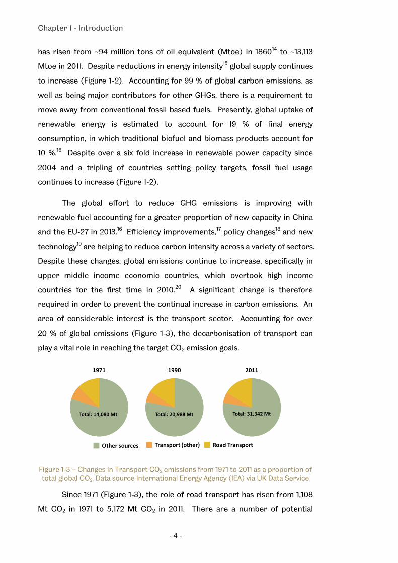
20 % of global emissions (Figure 1-3), the decarbonisation of transport can
play a vital role in reaching the target CO2 emission goals.
Figure 1-3 – Changes in Transport CO2 emissions from 1971 to 2011 as a proportion of total global CO2. Data source International Energy Agency (IEA) via UK Data Service
Since 1971 (Figure 1-3), the role of road transport has risen from 1,108
Mt CO2 in 1971 to 5,172 Mt CO2 in 2011. There are a number of potential

Chapter 1 - Introduction
- 5 -
options to achieve transport decarbonisation. In road vehicles, biofuels,
electrification and the use of hydrogen are all being considered.21 There is
much discussion regarding the viability and potential of each fuel to replace
conventional sources in vehicles22,23 however electric and hydrogen based
fuels have the benefit of zero emission at use, unlike biofuels. Electric
vehicles (EV) are significantly further progressed than their hydrogen
counterparts with a number of vehicles available for consumer purchase.
However, EV still face many challenges.24 The current carbon intensity of the
electricity market, the driving range of the vehicles themselves and consumer
attitudes towards the vehicles can be a limit to their widespread uptake.25
The energy density of hydrogen is such that the range of hydrogen
vehicles can be closer to conventional vehicles, with new vehicles from
Toyota and Hondo offering a 300 mile range, close to the 320 miles required
for US drivers.26 It has been postulated that climate change in its entirety is
the greatest pressure on mankind to adapt and alter societal behaviours27
and therefore hydrogen vehicles offer a clean alternative that reduces the
requirement for mass social change. This is not to say hydrogen vehicles are
issue free. Production costs and safety requirements28 in regards to the
infrastructure are still required to be overcome to ensure the uptake,
however pilot projects and commercial interest are pushing the technology
forward to become cost competitive.26,29,30
A major component of any secondary energy carrier, such as
electricity and hydrogen, is the source.31 Hydrogen is a commercially
produced commodity and with that, the knowledge surrounding production
techniques, efficiencies and handling is mature. This is a beneficial aspect of
a future hydrogen based transport system. However, current production
methods of hydrogen are energy and carbon intensive.32 Along with current
techniques, if hydrogen is to become a major fuel source for road
transportation, global production is required to significantly increase in order
to continue to meet the demands of current business requirements.
Renewable production of hydrogen arises in a few forms as a potential
alternative to meet the increased demand while ensuring the cycle remains

Chapter 1 - Introduction
- 6 -
carbon free. Clean hydrogen production can come from the use of
renewable electricity generation (wind/solar/wave) combined with a
conventional electrolyser or various solar techniques.33 As enough solar
energy reaches the Earth in 1 hour to meet global yearly power requirements,
solar hydrogen is an area of significant potential.34
1.2.1 Solar Hydrogen
Solar technologies have developed considerably with solar
photovoltaics achieving efficiencies greater than 38 % under standard
terrestrial conditions.35 There is also a great deal of potential for the wide
scale application of solar energy to provide more than current global
electricity requirements.36 In regards to implementing solar energy for
hydrogen production there a few pathways available, (i) solar photovoltaic
and electrolyser (ii) concentrated solar thermal and electrolyser (iii) thermo-
chemical (iv) biological processes and (v) photoelectrochemical (PEC).
Systems that combine an energy generation step with an electrolyser
such as (i) and (ii) rely on the efficiency of the initial generation step and that
of the electrolyser. With typical commercial electrolysers performing at
efficiencies of 73 %,37 even with the optimum solar cell a performance of
around 27 % is achievable, whereas for typical commercial silicon-PV it is
approximately 10 %. As it is technologically viable, it is definitely a promising
option. Currently there are issues surrounding land requirements and the
total cost of systems. Concentrated solar arrays can be utilised across all
solar devices leading to potential performance enhancements.38 However
direct photolysis is not a viable option, with temperatures of 4000 °C
required, higher than those typically achieved with concentrated systems.33
Due to the high temperatures required for direct photolysis, multi-
step thermo-chemical cycles have been investigated to reduce the required
temperature. These offer a promising route with potential efficiencies of
70 % achievable. The main focus has been via the use of metal oxide cycles, in
which ZnO is favourable due to a completion temperature of ~2000 °C.38 The
process operates via the decomposition of the metal oxide before the

Chapter 1 - Introduction
- 7 -
formation of ZnO via the introduction of H2O into the system, generating
hydrogen. The technological challenges facing the redox couples during the
process are of concern in order to produce a commercially viable system.33
Biological processes have received a considerable degree of interest39
and can work via photosynthesis or photo-fermentation. Photolytic
production with green algae or cyanobacteria is a direct process in which the
algae convert water molecules into hydrogen and oxygen during
photosynthesis. Although theoretical efficiencies of 80 % have been
postulated,40,41 this is unlikely due to the nature of the algae to self-assemble
and current values are less than 1 %. Photo-fermentation produces hydrogen
using light energy and organic acids. Algal based processes currently suffer
from low efficiencies and the requirements of specialised bioreactors to
achieve improved production rates.32
The above technologies all suffer from a range of issues including cost,
area requirements, feasibility and overall efficiencies.42 An alternative
technology that offers long term promise is photoelectrochemical production
of hydrogen in which an efficiency of over 12 % has been achieved.43
Figure 1-4 - Basic schematic of photoelectrochemical cell under operation
Photoelectrochemical Hydrogen
Photoelectrochemical production of hydrogen is a form of direct
photolysis in which water is split into the hydrogen and oxygen constituents
via the use of a semiconductor material and sunlight. At room temperature,
water splitting requires 1.23 V to form oxygen and hydrogen to overcome the

Chapter 1 - Introduction
- 8 -
reaction potentials. Due to surface interactions and losses within the system
this typically increases to between 1.6 and 1.8 V. Solar energy can be
sufficiently utilised for this process, as by converting the required energy into
a wavelength results in a value of ~690 nm, meaning almost the entire visible
spectra has sufficient energy to split water.
The process was first reported in 1972 by Fujishima and Honda,44 using
a TiO2 electrode. Typically semiconductor materials similar to those used in
photovoltaic applications have been investigated.43 The process can occur via
the use of a single semiconductor and metal electrode or two semiconductor
electrodes. The basic principle occurs when sunlight is absorbed via the
semiconductor material and unlike generating electricity as in photovoltaic
cells, splits the electrolyte solution into hydrogen and oxygen (Figure 1-4).
This process will be thoroughly described in Chapter 2.
In comparison to other production methods described, PEC has the
potential for wide-scale application due to the use of ambient temperatures,
relatively simple infrastructure and large energy resource. With an efficiency
of just 10 %, it is thought that around 0.1 % of US land mass would be required
to power the entire US fleet.43 Alongside these benefits, unlike algal systems,
there is the potential for compact systems, allowing small scale production
for domestic use as a vehicle fuel or energy store.45 Furthermore, the
potential of PEC systems is not limited solely to hydrogen production, with
developments of pollutant and CO2 treatment systems also being
investigated.46,47
1.3 Issues & Limitations
In order for photoelectrochemical hydrogen to succeed there are a
number of requirements that have to be satisfied. First, the semiconductor
material in use is required to have the correct band alignment to effectively
split water. Additionally the overall absorption efficiency is required to be at
least 80 % and it has to be able to withstand the chemical solutions
implemented over an adequate working timescale.42 Although over 40 years
since the initial discovery the progress is still far from ideal. Due to the total
Chapter 1 - Introduction
- 9 -
available materials numbering over 2 million,43 progress in search of the ideal
candidates has been limited. Advances in material design techniques have
allowed a greater variety of materials to be screened, increasing the rate at
which advances are made.48,49
Aside from process specific issues, the practicality of the material also
has to be considered. Requirements with regards to commercialisation are a
necessary issue in order to obtain a cost efficient device.50 If hydrogen is to
be widely utilised, production capacity is required to significantly increase.51,52
Any material implemented within a solar production route is required to have
sufficient capacity for wide-scale device production. III-nitride materials have
the potential to satisfy a number of these concerns.
1.4 III-Nitrides
The history of III-nitride based semiconductor materials originates
from the early 20th century with the discovery of both AlN and InN within the
space of three years.53,54 GaN was not reported until 1932,55 however it was
not until the 1990s, with the fabrication of a blue GaN light-emitting diode
(LED), that their potential began to be realised.56 Despite discovery in 1932,
single crystal GaN proved difficult to obtain and it was not until 1969 that it
was successfully grown via hydride vapour phase epitaxy (HVPE).57 The
challenge of growing high quality GaN resulted in a limited research focus,
demonstrated by the research plateau between the 70 and 80’s (Figure 1-5).
Invention of the low-temperature buffer techniques in 198658 resulted
in a significant increase the quality of the material being grown. The
technique works via the insertion of a thin nucleation layer of
aluminium/gallium nitride grown at a low temperature (LT). Grown directly
on foreign substrates (sapphire), GaN grows via three-dimensional islands
which all have slight misalignments with each other resulting in poor quality
films observed prior to the LT technique. At low temperature, two-
dimensional growth dominates resulting in improved optical, electrical and
structural characteristics.59 Shortly after, the technique allowed the growth
of p-type GaN, previously unobtainable.60,61 P-type GaN is grown via the

Chapter 1 - Introduction
- 10 -
addition of magnesium as a dopant, but is required to be activated in order to
achieve the necessary properties to be identified as a p-type
semiconductor.62
1970 1980 1990 2000 20101
10
100
1000
10000
solar cell
laser diode
commercial LED
p-type GaN
Blue LED
HVPE GaN
LT buffer
Pu
bli
ca
tio
ns
Lis
ted
Year
stimulated emission RT
Figure 1-5 – Number of publications (Web Of Knowledge) and development of GaN since 1969
A property of III-nitride materials is their miscible nature. Despite the
different material properties, aluminium, indium and gallium nitrides have the
ability to form binary and ternary alloys in any composition.63 As with GaN,
early alloys were of low quality64 and it was not until the incorporation of the
LT growth technique that band-to-band emission was observed.65
Development of both p- and n- type nitride materials and III-nitride alloys
resulted in the first p-n junction LED to be developed,62 leading to the
fabrication of high brightness double heterostructure blue LEDs in 1994.66
The interest in GaN materials has continued to increase with publications
increasing in significant numbers over the past two decades (Figure 1-5). This
has resulted in III-nitride materials taking a role in the development of Blu-ray
technology67 and in the fabrication of high efficiency LEDs.68 The contribution
of GaN to high brightness white LEDs places them at the forefront of solid-
state lighting and energy efficient displays.69 The constant development has
led to an increased understanding of the material properties and reduced
costs.
Chapter 1 - Introduction
- 11 -
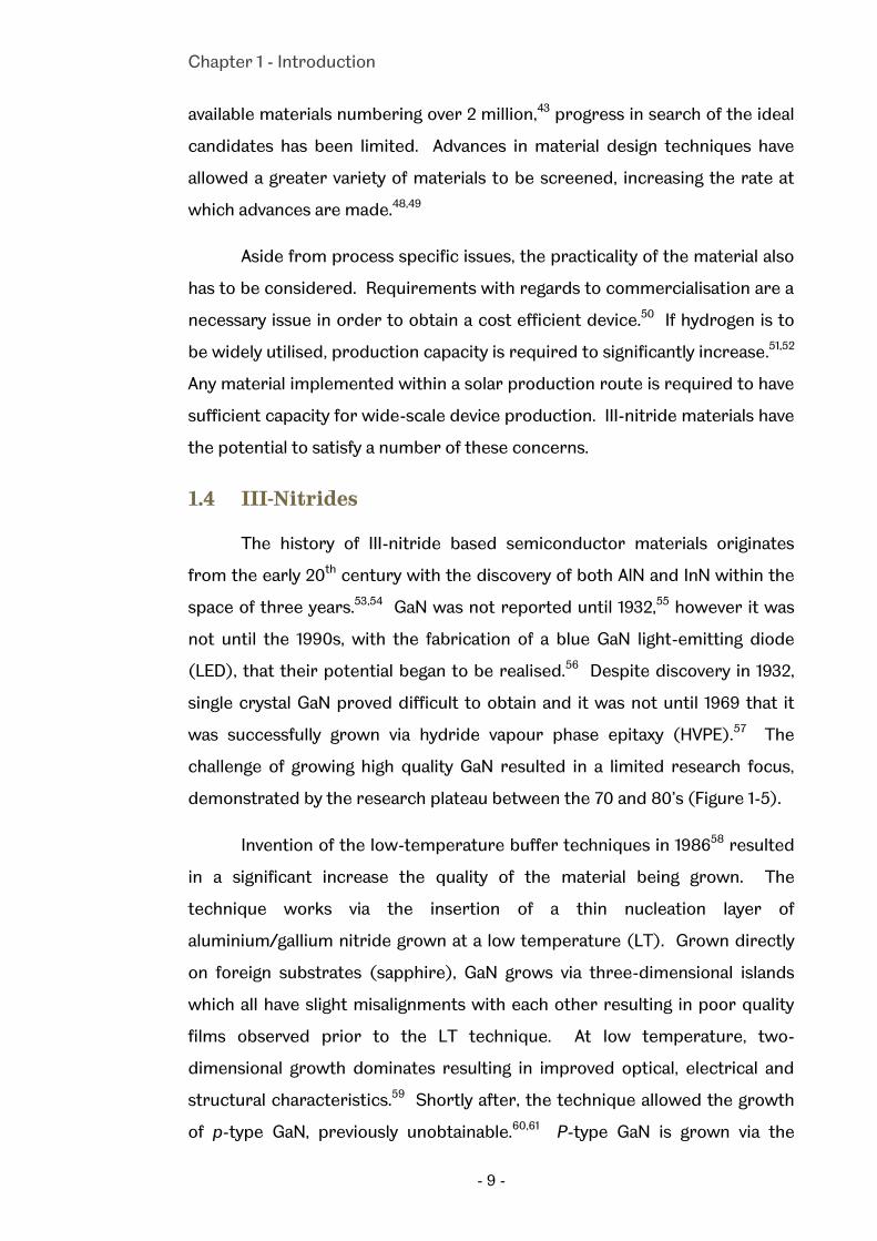
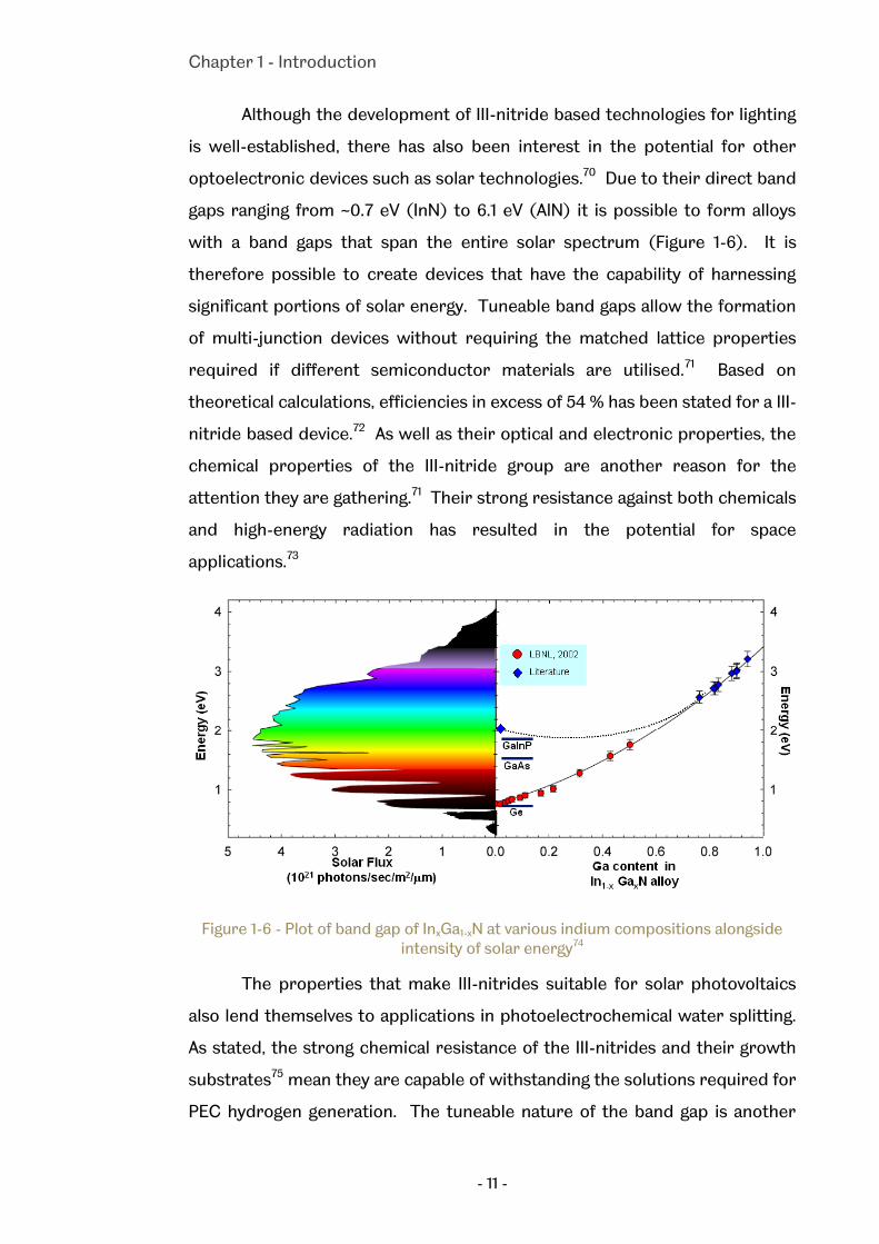
Although the development of III-nitride based technologies for lighting
is well-established, there has also been interest in the potential for other
optoelectronic devices such as solar technologies.70 Due to their direct band
gaps ranging from ~0.7 eV (InN) to 6.1 eV (AlN) it is possible to form alloys
with a band gaps that span the entire solar spectrum (Figure 1-6). It is
therefore possible to create devices that have the capability of harnessing
significant portions of solar energy. Tuneable band gaps allow the formation
of multi-junction devices without requiring the matched lattice properties
required if different semiconductor materials are utilised.71 Based on
theoretical calculations, efficiencies in excess of 54 % has been stated for a III-
nitride based device.72 As well as their optical and electronic properties, the
chemical properties of the III-nitride group are another reason for the
attention they are gathering.71 Their strong resistance against both chemicals
and high-energy radiation has resulted in the potential for space
applications.73
Figure 1-6 - Plot of band gap of InxGa1-xN at various indium compositions alongside intensity of solar energy74
The properties that make III-nitrides suitable for solar photovoltaics
also lend themselves to applications in photoelectrochemical water splitting.
As stated, the strong chemical resistance of the III-nitrides and their growth
substrates75 mean they are capable of withstanding the solutions required for
PEC hydrogen generation. The tuneable nature of the band gap is another

Chapter 1 - Introduction
- 12 -
benefit, but not the complete picture. To be discussed further in Chapter 2,
water splitting requires specific band positions in order to achieve the overall
reaction.76 GaN has these required band positions,77,78 as does InGaN alloys
up to a indium content of 50 %,79 allowing a significant portion of sunlight to
be absorbed, while effectively transferring energy into the water splitting
reaction.
Despite being identified as a potential material for water splitting in
2005,80 there has only been a limited number of groups investigating III-
nitrides for water splitting. Difficulties in the growth of high quality indium
gallium nitride71 mean alternative methods are required to achieve high
efficiency devices. The commercial outlook of III-nitrides for a wide variety of
applications, mean that economic prospects and quality is continuously
progressing. The ideal band positions and tuneable band gaps indicate the
strong potential for solar applications. There is therefore a great opportunity
to exploit this material for renewable technologies to reduce global carbon
emissions.

Chapter 1 - Introduction
- 13 -
Bibliography
1 A.S. Goudie, The Human Impact on the Natural Environment: Past, Present, and Future, Seventh (Wiley, Chichester, 2013).
2 A. Mikkelsen and O. Langhelle, Arctic Oil and Gas Sustainability At Risk? (Routledge, Abingdon, 2008).
3 M. Landon, Environment, Health And Sustainable Development, Illustrate (McGraw-Hill Education, New York, 2006).
4 F. Harris, Global Environmental Issues, Second (Wiley, Chichester, 2012).
5 K.C. Kim and R.D. Weaver, Biodiversity and Landscapes: A Paradox of Humanity, Illustrate (Cambridge University Press, Cambridge, 1994).
6 R. Lee, S. The, E. Perspectives, and N. Autumn, J. Econ. Perspect. 17, 167 (2003).
7 P.M. Vitousek, H.A. Mooney, J. Lubchenco, and J.M. Melillo, Science 277, 494 (1997).
8 D. of E. and S.A. United Nations, World Population Prospects The 2010 Revision (New York, 2011).
9 U. Cubasch, D. Wuebbles, D. Chen, M.C. Facchini, D. Frame, N. Mahowald, and J.-G. Winther, in Clim. Chang. 2013 Phys. Sci. Basis. Contrib. Work. Gr. I to Fifth Assess. Rep. Intergov. Panel Clim. Chang., edited by T.F. Stocker, D. Qin, G.-K. Plattner, M. Tignor, S.K. Allen, J. Boschung, A. Nauels, Y. Xia, V. Bex, and P.M. Midgley (Cambridge University Press, Cambridge, 2013), pp. 119–158.
10 R.J. Nicholls and A. Cazenave, Science 328, 1517 (2010).
11 D.L. Hartmann, A.M.G.K. Tank, M. Rusticucci, L.V. Alexander, S. Brönnimann, Y. Charabi, F.J. Dentener, E.J. Dlugokencky, D.R. Easterling, A. Kaplan, B.J. Soden, P.W. Thorne, M. Wild, and P.M. Zhai, in Clim. Chang. 2013 Phys. Sci. Basis. Contrib. Work. Gr. I to Fifth Assess. Rep. Intergov. Panel Clim. Chang., edited by T.F. Stocker, D. Qin, G.-K. Plattner, M. Tignor, S.K. Allen, J. Boschung, A. Nauels, Y. Xia, V. Bex, and P.M. Midgley (Cambridge University Press, Cambridge, 2013), pp. 159–254.
12 M.G.J. den Elzen. and M. Meinshausen, Meeting the EU 2°C Climate Target: Global and Regional Emission Implications (AH Bilthoven, 2005), pp. 1–44.
13 G. Resch, A. Held, T. Faber, C. Panzer, F. Toro, and R. Haas, Energy Policy 36, 4048 (2008).

Chapter 1 - Introduction
- 14 -
14 H.-D. Haustein and E. Neuwirth, Technol. Forecast. Soc. Change 22, 53 (1982).
15 T.C. Bond, E. Bhardwaj, R. Dong, R. Jogani, S. Jung, C. Roden, D.G. Streets, and N.M. Trautmann, Global Biogeochem. Cycles 21, 1 (2007).
16 REN21, Renewables 2014 Global Status Report (Paris, 2014).
17 E. Worrell, L. Bernstein, J. Roy, L. Price, and J. Harnisch, Energy Effic. 2, 109 (2008).
18 H. Bulkeley and K. Kern, Urban Stud. 43, 2237 (2006).
19 J.D. Figueroa, T. Fout, S. Plasynski, H. McIlvried, and R.D. Srivastava, Int. J. Greenh. Gas Control 2, 9 (2008).
20 D. Victor, D. Zhou, E.H.M. Ahmed, P.K. Dadhich, J. Olivier, H.-H. Rogner, K. Sheikho, M. Yamaguchi, G. Baiocchi, Y. Mulugetta, and L. Wong, in Clim. Chang. 2014 Mitig. Clim. Chang. Contrib. Work. Gr. III to Fifth Assess. Rep. Intergov. Panel Clim. Chang., edited by A. Grubler and A. Muvundika (Cambridge University Press, Cambridge, 2014), pp. 1–63.
21 S. Kobayashi, S. Plotkin, and S.K. Ribeiro, Energy Effic. 2, 125 (2009).
22 C. Winter, Int. J. Hydrogen Energy 30, 1371 (2005).
23 F.H. Sobrino, C.R. Monroy, and J.L.H. Pérez, Renew. Sustain. Energy Rev. 14, 772 (2010).
24 S. Steinhilber, P. Wells, and S. Thankappan, Energy Policy 60, 531 (2013).
25 S. Carley, R.M. Krause, B.W. Lane, and J.D. Graham, Transp. Res. Part D Transp. Environ. 18, 39 (2013).
26 R.K. Ahluwalia, X. Wang, a Rousseau, and R. Kumar, J. Power Sources 130, 192 (2004).
27 C. Vlek and L. Steg, J. Soc. Issues 63, 1 (2007).
28 R. Shinnar, Technol. Soc. 25, 455 (2003).
29 C. Winter, Int. J. Hydrogen Energy 30, 681 (2005).
30 M.H. Maack and J.B. Skulason, J. Clean. Prod. 14, 52 (2006).
31 M. Ball and M. Wietschel, Int. J. Hydrogen Energy 34, 615 (2009).
32 R. Chaubey, S. Sahu, O.O. James, and S. Maity, Renew. Sustain. Energy Rev. 23, 443 (2013).

Chapter 1 - Introduction
- 15 -
33 T. Abbasi and S. a. Abbasi, Renew. Sustain. Energy Rev. 15, 3034 (2011).
34 N.S. Lewis and D.G. Nocera, Proc. Natl. Acad. Sci. U. S. A. 103, 15729 (2006).
35 M.A. Green, K. Emery, Y. Hishikawa, W. Warta, and E.D. Dunlop, Prog. Photovoltaics Res. Appl. 22, 1 (2014).
36 G.R. Timilsina, L. Kurdgelashvili, and P. a. Narbel, Renew. Sustain. Energy Rev. 16, 449 (2012).
37 S.K. Mazloomi and N. Sulaiman, Renew. Sustain. Energy Rev. 16, 4257 (2012).
38 E. Bozoglan, A. Midilli, and A. Hepbasli, Energy 46, 85 (2012).
39 A. Bahadar and M. Bilal Khan, Renew. Sustain. Energy Rev. 27, 128 (2013).
40 A. Ley and D. Mauzerall, Biochim. Biophys. Acta (BBA)-Bioenergetics 680, 95 (1982).
41 V. Shah, N. Garg, and D. Madamwar, FEMS Microbiol. Lett. 194, 71 (2001).
42 J.D. Holladay, J. Hu, D.L. King, and Y. Wang, Catal. Today 139, 244 (2009).
43 J. Turner, G. Sverdrup, M.K. Mann, P. Maness, B. Kroposki, M. Ghirardi, R.J. Evans, and D. Blake, Int. J. Energy Res. 32, 379 (2008).
44 A. Fujishima and K. Honda, Nature 238, 37 (1972).
45 T. Bak, J. Nowotny, M. Rekas, and C. Sorrell, Int. J. Hydrogen Energy 27, 991 (2002).
46 Y. Du, Y. Feng, Y. Qu, J. Liu, N. Ren, and H. Liu, Environ. Sci. Technol. (2014).
47 B. Kumar, M. Llorente, J. Froehlich, T. Dang, A. Sathrum, and C.P. Kubiak, Annu. Rev. Phys. Chem. 63, 541 (2012).
48 K. Kim, P. A. Graf, and W.B. Jones, J. Comput. Phys. 208, 735 (2005).
49 Z. Chen, T.F. Jaramillo, T.G. Deutsch, A. Kleiman-Shwarsctein, A.J. Forman, N. Gaillard, R. Garland, K. Takanabe, C. Heske, M. Sunkara, E.W. McFarland, K. Domen, E.L. Miller, J. a. Turner, and H.N. Dinh, J. Mater. Res. 25, 3 (2011).
50 G. Marbán and T. Valdés-Solís, Int. J. Hydrogen Energy 32, 1625 (2007).
51 S. Blanchette, Energy Policy 36, 522 (2008).
52 J. Hetland and G. Mulder, Int. J. Hydrogen Energy 32, 736 (2007).
53 F. Fichter, Zeitschrift Für Anorg. Chemie 54, 322 (1907).

Chapter 1 - Introduction
- 16 -
54 F. Fischer and F. Schröter, Berichte Der Dtsch. Chem. Gesellschaft 43, 1465 (1910).
55 W.C. Johnson, J.B. Parson, and M.C. Crew, J. Phys. Chem. 36, 2651 (1932).
56 O. Ambacher, J. Phys. D. Appl. Phys. 31, 2653 (1998).
57 H.P. Maruska, Appl. Phys. Lett. 15, 327 (1969).
58 H. Amano, N. Sawaki, I. Akasaki, and Y. Toyoda, Appl. Phys. Lett. 48, 353 (1986).
59 I. Akasaki, J. Cryst. Growth 195, 248 (1998).
60 H. Amano, I. Akasaki, T. Kozawa, K. Hiramatsu, N. Sawaki, K. Ikeda, and Y. Ishii, J. Lumin. 40-41, 121 (1988).
61 H. Amano, J. Electrochem. Soc. 137, 1639 (1990).
62 H. Amano, M. Kito, K. Hiramatsu, and I. Akasaki, Jpn. J. Appl. Phys. 28, L2112 (1989).
63 J.I. Pankove, Mater. Sci. Eng. B 61-62, 305 (1999).
64 N. Yoshimoto, T. Matsuoka, T. Sasaki, and a. Katsui, Appl. Phys. Lett. 59, 2251 (1991).
65 S. Nakamura and T. Mukai, Jpn. J. Appl. Phys. 31, L1457 (1992).
66 S. Nakamura, T. Mukai, and M. Senoh, Appl. Phys. Lett. 64, 1687 (1994).
67 H. Amano, Jpn. J. Appl. Phys. 52, 050001 (2013).
68 S. Nakamura and M.R. Krames, Proc. IEEE 101, 2211 (2013).
69 S.P. DenBaars, D. Feezell, K. Kelchner, S. Pimputkar, C.-C. Pan, C.-C. Yen, S. Tanaka, Y. Zhao, N. Pfaff, R. Farrell, M. Iza, S. Keller, U. Mishra, J.S. Speck, and S. Nakamura, Acta Mater. 61, 945 (2013).
70 K. Tanabe, Energies 2, 504 (2009).
71 J. Wu, J. Appl. Phys. 106, 011101 (2009).
72 A. D. Vos, "Endoreversible Thermodynamics of Solar Energy Conversion" (Oxford University Press, 1992), p. 90.
73 J. Wu, W. Walukiewicz, K.M. Yu, W. Shan, J.W. Ager, E.E. Haller, H. Lu, W.J. Schaff, W.K. Metzger, and S. Kurtz, J. Appl. Phys. 94, 6477 (2003).

Chapter 1 - Introduction
- 17 -
74 W. Walukiewicz, Future Prospects of Semiconductor Materials for Solar and Photoelectrochemical Cells, LBNL Workshop, March 28-29, Berkeley, California, USA (2005).
75 S. Strite and H. Morkoc ̧̌, J. Vac. Sci. Technol. B Microelectron. Nanom. Struct. 10, 1237 (1992).
76 T. Hisatomi, J. Kubota, and K. Domen, Chem. Soc. Rev. (2014).
77 J.W. Ager III, J. Wu, K.M. Yu, R.E. Jones, S.X. Li, W. Walukiewicz, E.E. Haller, H. Lu, and W.J. Schaff, in Fourth Int. Conf. Solid State Light., edited by I.T. Ferguson, N. Narendran, S.P. DenBaars, and J.C. Carrano (2004), pp. 308–315.
78 I.M. Huygens, K. Strubbe, and W.P. Gomes, J. Electrochem. Soc. 147, 1797 (2000).
79 P.G. Moses and C.G. Van de Walle, Appl. Phys. Lett. 96, 021908 (2010).
80 K. Fujii, T. Karasawa, and K. Ohkawa, Jpn. J. Appl. Phys. 44, L543 (2005).

Chapter 1 - Introduction
- 18 -

Chapter 2 - Background
- 19 -
Chapter 2
Background
general theory of the various areas of science are presented from
basic semiconductor physics through to a focus of
photoelectrochemical water splitting. It serves as an introduction into each
research topic with more specific information provided in the subsequent
result chapters.
2.1 Semiconductors
Semiconductors are a class of materials whose electrical conductivity
is between metals and insulators and can be composed of atomic elements,
inorganic compounds, such as GaAs, or organic materials. The resistivity of
semiconductors is at a value between 104 and 10-10 Ωcm1. Inorganic
semiconductors are typically bonded via covalent bonds. The covalent nature
arises due to a sharing of electrons, either between heterogeneous (GaN,
Fe2O3) or homogeneous (Si, Ge, C) species. Elements are comprised of
electrons, neutrons and protons. While the protons and neutrons reside in
the nucleus, the electrons form discrete energy bands around the nucleus,
known as orbitals. Each orbital can hold a maximum number of degenerate
electrons specific to the orbital type. In increasing energy the orbitals are the
s (2), p (6), d (10), f (14), g (18) and h (22) with the number of electrons
identified in parenthesis. No currently discovered element has ground state
A

Chapter 2 - Background
- 20 -
electrons in the g or h orbitals. For the majority of semiconductor materials,
it is the s, p and d orbitals that are of concern. The energetically favourable
state for atoms is to have a completely filled outer orbital. Taking silicon as
an example, there are a total of 14 electrons within atomic silicon. These
electrons sit in the 1s (2), 2s (2), 2p (6), 3s (2) and 3p (2) orbitals. From this it
is clear that the 3p orbital contains only 2 of the required 6 electrons. In
order to satisfy a filled orbital, 4 further electrons are required. This occurs
via the formation of covalent bonds in which atomic silicon shares electrons
with other silicon atoms, in order to have a total of 8 electrons in the outer
orbital. The nature of the bonding across the semiconductor material class
varies to some degree. The extent of covalent (shared electrons) and ionic
(donor/acceptor electrons) bonding changes across the group which
ultimately alters the material properties.2
Figure 2-1 – Illustration of metal, semiconductor and insulator band structures
Due to the Pauli Exclusion Principle, it is only possible to have a
maximum of two electrons (of opposite spin) with the same discrete energy
level in a system. Therefore, when n atoms are brought together, n energy
bands are formed. The formed energy states are allowed positions for the
electrons to exist. Between these positions lie forbidden regions in which
electrons are not allowed to occupy. The conduction of semiconductors is
derived from the formation of these energy bands. At 0 K, electrons are in
the first allowed energy band, the valence band, while no electrons are
present in the conduction band, similar to that of an insulator (Figure 2-1). In
Chapter 2 - Background
- 21 -
contrast, in a metal, the empty conduction band overlaps the valence band
and therefore in a sense, there is one partially filled band (Figure 2-1). In
order for conduction to occur, a band can neither be completely filled or
empty. Therefore, generally speaking, metals have the ability to conduct at
any temperature as a result of the available allowed energy states. Unlike
insulators, in which the gap between the bands is sufficiently large to prevent
promotion, an input of energy to a semiconductor will excite electrons from
the valence band to the conduction band. The difference between the
valence and conduction band is known as the band gap, which is a
fundamental parameter to describe semiconductors.
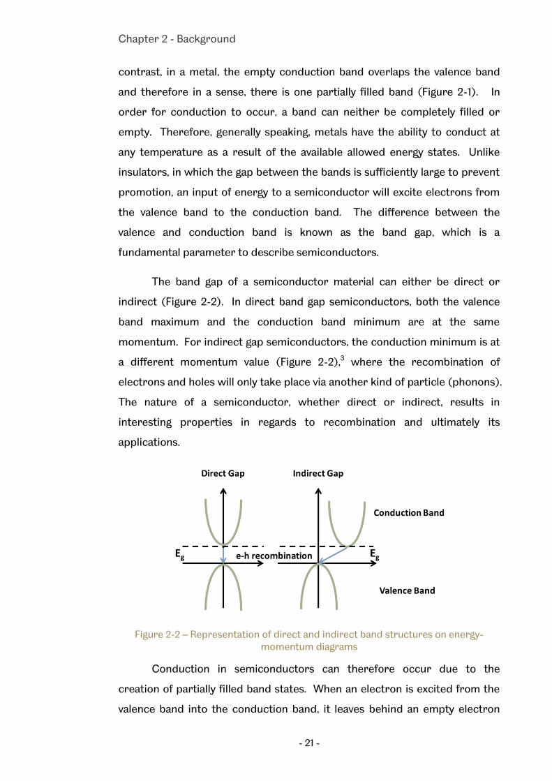
The band gap of a semiconductor material can either be direct or
indirect (Figure 2-2). In direct band gap semiconductors, both the valence
band maximum and the conduction band minimum are at the same
momentum. For indirect gap semiconductors, the conduction minimum is at
a different momentum value (Figure 2-2),3 where the recombination of
electrons and holes will only take place via another kind of particle (phonons).
The nature of a semiconductor, whether direct or indirect, results in
interesting properties in regards to recombination and ultimately its
applications.
Figure 2-2 – Representation of direct and indirect band structures on energy-momentum diagrams
Conduction in semiconductors can therefore occur due to the
creation of partially filled band states. When an electron is excited from the
valence band into the conduction band, it leaves behind an empty electron

Chapter 2 - Background
- 22 -
state known as a hole. In intrinsic semiconductors (undoped) there exist a
similar number of electrons in the conduction band as there are holes in the
valence band due to thermal excitation at room temperature. Another
property of semiconductors is their ability to be doped by additional
materials. Doped semiconductors can have an excess of electrons or holes
depending on the dopant. Replacing one atom in the crystal structure with
one of higher or lower outer orbital electron, results in an almost free
electron or hole in the device respectively. Doping materials will create an n-
type or p-type semiconductor depending on whether there are additional
electrons (n-type) or holes in the crystal structure (p-type). In order to
describe semiconductors fully, another important concept needs to be
introduced, namely the Fermi level (EF). In an intrinsic semiconductor, the
Fermi level is in about the centre of the forbidden region. Deviation from this
point within the forbidden region depends on the effective mass of electrons
and holes. Generally speaking, for n-doped semiconductors, the Fermi level
rises to a level close to the conduction band while for p-type it falls to a level
close to the valence band.
2.1.1 Conduction, Mobility and Recombination
As stated, electrons and holes are responsible for the conduction in
semiconductor materials. There are two mechanisms behind this process,
drift and diffusion. Drift is the result of an electric field acting on the carriers,
while diffusion is caused by a concentration gradient. The influence of drift is
controlled via the strength of the electric field exerted on the electrons and
holes. The drift velocity of a semiconductor is a product of the electric field
(E) and the mobility (µ), in which mobility is the measure of carriers’ ability to
move.4 There are a number of scattering mechanisms, which will limit a
further increase in velocity with an increase in the applied electric field. This
is potentially through defects and collective vibrations of lattice atoms, due to
thermal energy, which can be described in the form of phonons. As a result
of these limits, a saturation level is reached, which is called the saturation
velocity and is dependent on the material.5

Chapter 2 - Background
- 23 -
In a typical semiconductor device under operation, an electric field
and concentration gradient will exist. The total current is therefore
determined by both drift and diffusion. A change in carriers away from
equilibrium is ultimately only temporary. In regards to semiconductors, the
relaxation back to equilibrium conditions occurs via a process known as
recombination. The generated electron and hole pairs recombine, returning
back to the undisturbed state. Recombination is controlled in part by the
diffusion length of the carriers. Upon injection, in doped semiconductors, the
majority carrier concentration changes by an insignificant amount but there
is a drastic change in minority carriers. Therefore the minority carriers
dominate and the recombination rate is proportional to the population and
lifetime of these carriers.6 As discussed, carriers after injection will move via
diffusion principles, combination with a lifetime, results in the carriers having
a specific diffusion length. This property plays a crucial role in
semiconductor device efficiencies.
There are a number of mechanisms that affect recombination and
these can be material dependent.5 Recombination via the emission of a
photon is known as radiative recombination which can occur via various
mechanisms (Figure 2-4). As illustrated in Figure 2-4, process i-ii indicates
the excitation of an electron into the conduction band, rapid thermalisation
and then recombination. In process iii, a free exciton or impurity bound
exciton decays into the valence band. Processes iv-vi indicate the presence of
neutral states within the material, either acceptor or donor states, in which
transitions can occur.7 These donor states may be present due to doping
within the semiconductor. Not all recombination processes proceed via
photon emission and nonradiative processes occur via three dominant
mechanisms, transformation into heat, creation of defects and
photochemical changes of the material.8 The presence of nonradiative
pathways can result in a decreased efficiency of a semiconductor device.
Nonradiative recombination can occur via the presence of trap states
between the conduction and valence bands due to defects or impurities
(Shockley-Read-Hall) or via an Auger process.9 Auger processes involve the

Chapter 2 - Background
- 24 -
transmission in the recombination energy to another electron or hole,
resulting in a change to the kinetic energy of the system. It is a particularly
important aspect in regards to light emitting diodes due to high carrier
densities.
Figure 2-4 – Radiative recombination mechanisms in semiconductors7
2.1.3 Optical Properties
Electromagnetic radiation in the form of light is both an interesting
feature of semiconductors as well as a useful diagnostic tool.10 Spectroscopic
techniques can provide information regarding the band gap of the
semiconductor due to the radiative recombination processes occurring
within the material. When a semiconductor is illuminated, a number of
processes occur at the interface. Some of the incident radiation will be
reflected and the rest transmitted through the sample. Unlike metals, the
reduced number of free energy carriers in semiconductors means that until
the incident wavelength is larger than the semiconductor band gap, no
significant absorption occurs.5 Therefore, via the use of absorption
spectroscopy, information can be inferred regarding the band gap of the
material due to the absorption or transmission level of each defined
wavelengths.
During optical injection, when carriers recombine, the emitted
radiation as photons is known as photoluminescence. Photoluminescence
can occur via two mechanisms, fluorescence and phosphorescence and is a
significant process in semiconductors. Fluorescence is a direct energy

Chapter 2 - Background
- 25 -
transfer from singlet states, while phosphorescence involves an intermediary
step in which the energy is transferred into a forbidden energy state. As a
result of the differences in energy transfer routes, fluorescence is typically a
very fast process dependent on band structure and whether it is stimulated
or spontaneous emission, while phosphorescence can last for significantly
longer periods after the initial injection.5 Photoluminescence spectroscopy
(PL) is the study of the radiative recombination processes (Figure 2-4) via the
excitation of carriers using light and is a common diagnostic tool for
semiconductors.
Alternative methods of injection involve the use of high energy electron
beams or electric currents. The processes in which the energy causes light
emission are known as cathodoluminescence and electroluminescence
respectively.5 Each spectroscopic technique provides an insight into the
described recombination processes and through advanced techniques, such
as time resolved photoluminescence, information regarding rates of decay
can be investigated. The specific techniques implemented in this thesis will
be described in further detail in the experimental section to provide relevant
and useful information pertaining to the theory and method.
2.1.4 Semiconductor-Metal Interface
As discussed, it is possible to inject carriers into a semiconductor via a
metal. When a metal and semiconductor are brought into contact, there are
a number of material properties that are required to be considered. The
work function (Ø) of the material is a critical property in determining
whether the metal-semiconductor interface will be ohmic or Schottky.11 The
work function, as depicted in Figure 2-5 is the minimum amount of energy
required to take an electron from a solid into the vacuum. If ØM>ØS a
potential barrier is created when the metal and semiconductor are brought
into contact. This occurs as the Fermi levels are required to be in
coincidence forcing the semiconductor valence and conduction bands to
bend upwards. When the work function of the semiconductor is larger than
that of the metal, the conduction bands bend downwards (Figure 2-5),

Chapter 2 - Background
- 26 -
removing the barrier, allowing current flow in either direction, thus creating
an ohmic contact.12
Figure 2-5 – Schematic representation of metal-semiconductor (n-type) band structures when separated and in intimate ohmic contact
2.2 III-Nitride Semiconductors
The III-nitride semiconductor family is comprised of Ga, In and AlN
with ternary and quaternary structures also available.13 These are all of a
direct band gap structure, with their band gaps covering a wide spectral
region from deep UV (~200 nm) through to infrared (1770nm), including the
complete visible part of solar spectrum. III-nitrides could therefore
potentially be the best candidates for the fabrication of high performance
optoelectronics for future energy saving applications. This can include solar
energy applications, use in solid state lighting to replace general illumination
lighting sources and solar hydrogen generation. The pioneering work of
Akasaki and Nakamura the in late 1980s14,15 and early 1990s16 has resulted in
GaN and its alloys to become established as the industry’s preferred
semiconductor materials for short-wavelength emitters over the last two
decades.17,18 The major achievements are however limited to violet/blue
emitters. Furthermore, there still exist a number of scientific and
technological challenges, limiting their potentially overwhelming advantages,
to be explored. Typical examples of this are within solar applications where
the energy efficiency of III-nitride devices is far behind the theoretical
predictions.

Chapter 2 - Background
- 27 -
2.2.1 Structural Properties
The III-nitrides can form a wurtzite, zinc blende or rock salt crystal
structure (Figure 2-6), with wurtzite the thermodynamically stable structure
under ambient conditions. The cubic zinc blende structure has been grown
with the aid of cubic substrates to overcome the thermodynamic tendency to
form the hexagonal wurtzite structure.13 The stability of the wurtzite
structure is thought to arise from the electrostatic interactions between the
anions and cations (dashed lines Figure 2-6 (b)) as a result of the ionicity of
the III-nitrides.19 As discussed previously, the bonding within semiconductors
is typically covalent in nature. However, if the electronegativity of the two
bonding species is significantly different, a degree of ionicity in the bonding
can arise. In this case, a dipole moment may form resulting in a more
donation-acceptance nature of the bond. This is true for the III-nitrides in
which the electrons are typically found around the nitrogen atoms.20 Due to
these properties, under high pressures, the ionic nature wins out and results
in the phase transition to the rock salt structure (Figure 2-6 (c)).13
Figure 2-6 – Atomic structures of different crystal structures (a) zinc blende (b) wurtzite (c) rock salt
The structural properties of the III-nitrides such as the lattice constant
and thermal requirements for growth have resulted in difficulty in finding
suitable growth substrates. The high temperature required for epitaxial
growth has resulted in the wide spread use of sapphire as the growth
substrate, however due to the differences in thermal expansion coefficients
and the lattice mismatch of the materials, typical films of III-nitrides are liable

Chapter 2 - Background
- 28 -
to a level of strain.21 Recently, silicon as a substrate for epitaxial growth of
GaN is developing due to the complimentary applications, however the issue
of strain is an even more severe issue than for growth on sapphire, which is
leading to massive cracking of the epitaxial layers.22
2.2.2 Band Gaps
The III-nitride semiconductors have direct band gaps that range from
0.7 eV up to 6.2 eV making them applicable to a wide range of applications.
The initial belief was that InN had a band gap of 1.9 eV, instead of the actual
0.7 eV, due to the difficulty in growing high quality samples and this resulted
in confusion over the band structures of the alloys of indium as well.23 The
band gap of GaN was found to be 3.5 eV for the wurtzite structure however
this changes slightly for zinc blende GaN as a result of symmetry
differences.23 For AlN the room temperature obtained band gap for a high
quality sample has a value of 6.2 eV.21 With any mix of III-nitride materials
possible, semiconductors with direct band gaps of 0.7 eV through to 6.2 eV
are feasible. Detailed band structures have been investigated for each of the
nitrides exploring the specific nature of the electronic transitions that arise.23
The band gaps of the III-nitrides all show a degree of temperature
dependence which can be expressed by the Varshni formula (Equation 2-1).19
𝐸𝑔(𝑇) = 𝐸𝑔(0) −𝛼𝑇2
𝑇 + 𝛽
Equation 2-1 – Varshni formula for band gap variation with temperature where α and β are material specific parameters
2.2.3 Growth
As stated in the introduction, there were a number of breakthroughs
in growth technology that has allowed the commercial use of III-nitrides. Due
to lack of native substrates, III-nitrides are generally epitaxially grown on
foreign substrates, predominantly on sapphire.24 Due to the extremely large
lattice-mismatch between GaN and sapphire (up to 16%), III-nitride growth
remains a significant challenge. Despite this there have been developments in
regards to growth techniques on alternative substrates, such as Si, SiC, AlN
and GaN.

Chapter 2 - Background
- 29 -
The typical growth technique of the III-nitrides is via metal organic
chemical vapour deposition (MOCVD). This is a technique that allows the
deposition of controlled films onto a growth substrate resulting in the
formation of the semiconductor crystal. MOCVD uses chemical feedstock as
the source of the semiconductor molecules. High quality reactants are
vaporised and injected into the reactor where the specific growth conditions
have been set. This includes the growth temperature, flow rates of reactants
and reactor pressure. The injected reactants are elevated to decomposition
temperatures by the susceptor which results in the formation of thin films of
the desired compound semiconductor.25
For growth of III-nitrides, the traditional reactant gases or precursors
are trimethyl- variants ((CH3)3M where M=In, Al, Ga) and ammonia (NH3).26
The deposition process can then proceed via the elimination of alkane
radicals upon heating. The growth temperature of each III-nitride varies and
is one reason for the difficulty in growing high quality InN. For InGaN, a value
in excess of 600 °C is commonly utilised while GaN and AlN require
temperatures of at least 1000 °C.26 The ratio of the III/V elements is also a
crucial factor in controlling the growth with high ratios used in the growth of
GaN. The initial problems in growing GaN were overcome via the
implementation of a low temperature AlN (and later GaN) buffer layer with a
typical thickness of 25 nm,14 on the sapphire substrate prior to the GaN
growth. The growth layer has to be accurately controlled in order to result in
the observed improvements in surface roughness which paved the way for
the growth of p-type GaN. This resulted from the generation of nucleation
sites of the thin AlN which aided the directionally controlled growth of the
subsequent GaN layer. Our group has developed a technique using a high
temperature AlN buffer,27 which can further improve the crystal quality of
GaN and also eliminate the strict requirements for the thickness of the
nucleation layer in the two-step approach.
Further improvement in crystal quality of GaN can be obtained by
means of epitaxial lateral overgrowth (ELOG) and the techniques evolved
from ELOG overgrowth techniques,26 where a complicated ex-situ mask

Chapter 2 - Background
- 30 -
patterning process is involved.28 Overgrowth techniques are based on
selective area growth, and require the use of a dielectric mask such as SiO2
or Si3N4 via ex-situ processes, which is patterned into stripes on a micro
meter scale using a standard photolithography.29 The dislocations under the
mask stripes, caused by the large lattice-mismatch are effectively blocked.
However, it potentially causes non-uniformity issues and an atomically flat
surface cannot be obtained till the overgrown layer is 10-20 µm thick. As a
result there are still issues to be addressed for wide scale application of this
technique. The advances that have been made in the growth of III-nitrides
have resulted in the ability to grow larger higher quality wafers for various
applications improving their commercial applications.30
Doping
Presently, nominally undoped GaN exhibits n-type characteristics with
a typical background carrier concentration in the region of 1016 cm-3. As a
result of the existence of a large number of defects such as Ga or N vacancies,
dislocations arise with a typical of density of 108-109 cm-3. For the generation
of n-type GaN, an additional electron is required, either via the replacement
of a nitrogen or gallium site in the lattice. Silicon is the dopant of choice due
to the level of control it provides over the final carrier concentration.31 The
silicon replaces Ga sites in the lattice, adding the required electron for n-type
materials making it possible to dope the ternary nitride alloys of AlGaN and
InGaN. Doping of the material is controlled by altering the flow of silane
(SiH4) during MOCVD growth.
Unlike n-type GaN, the growth of p-type GaN proved difficult as the
majority of potential acceptor materials were all deep level acceptors
preventing the growth of a conducting p-type material.32 Substitution of
gallium sites with divalent magnesium, via biscyclopentadienyl magnesium
(CP2Mg), provides good control over the dopant level. However, the
magnesium is typically required to be activated due to the presence of H2 in
the reactor, which forms Mg-H complexes leading to passivation of the
material. Activation was initially found via the use of an electron beam33 and
later in the early 1990s Nakamura developed an annealing process in a high

Chapter 2 - Background
- 31 -
temperature N2 atmosphere. 34 The high energy process causes the Mg-H
complex to break and removes the H+ preventing further formation of the
complex. The breakthrough based on the simple but cost-effective
technology represents a milestone in the fields of III-nitrides, which laid a
solid foundation for the current III-nitride industry.
2.2.4 III-nitride Devices
Semiconductor based optoelectronics,30,32,35,36 in particular, LEDs or
LDs, generally consist of n-type regions, an active emitting region and p-type
regions. Low dimension structures, such as quantum well or quantum dots,
are generally used as the emitting region. Furthermore, correct metals need
to be selected in order to form good ohmic contacts on the devices.
Quantum Wells
For III-nitride devices, quantum well (QW) structures are commonly
utilised.21,37–40 A two-dimensional dimensional quantum well structure, are a
typical double heterostructure which consists of a thin layer with a low band
gap material as a quantum well sandwiched between two layers of larger
band gap material that serve as barriers.41 The quantum well thickness needs
to be smaller than the de Broglie wavelength of the material, leading to the
generation of a two-dimensional quantum confinement effect along the
growth direction, for simplicity, denoted as Z direction.
The quantum confinement effect leads to the generation of a number
of extra discontinuous energy levels in both valence and conduction bands as
shown in Figure 2-7 (a). This is dependent on the discontinuity of the band
gaps of quantum well and barrier which is denoted as the band-offset.
Accordingly, these extra energies are quantization energies, which can be
tuned by modifying the quantum well thickness. The optical transitions
between the sub bands in the conduction and valence band must follow a
selection rule, namely, n=0, 2, 4, ...., where n is the difference of the sub
band indices. In bulk material, vertical transitions conserve the momentum
but can have different energies. This results in the optical absorption being
related to the density of states, following a rise with the square root of

Chapter 2 - Background
- 32 -
energy.36 For quantum wells the density of states for in-plane motion is
constant with energy, resulting in the formation of steps, therefore the
optical absorption in keeping with the density of states, occurs stepwise for
each quantum number (Figure 2-7(b)).10
Figure 2-7 – (a) Simple model of optical absorption in quantum wells (b) density of states for a bulk (dashed) and quantum well semiconductor
InGaN quantum wells have been widely used as an emitting region in
the growth and fabrication of visible emitters. Although a number of major
achievements have been made within the last two decades, there are still a
number of challenges in regards to both the science and technology of the
devices. It is currently difficult to incorporate high levels indium into GaN in
order to form InGaN with emission towards green, yellow, or even longer
wavelengths.42 Currently, reducing the growth temperature for InGaN has
been widely used in order to enhance indium incorporation, but it leads to a
severe degradation in crystal quality of InGaN layer. As a result of the large
lattice-mismatch between InGaN and GaN when forming InGaN/GaN
quantum well structures on the widely used c-plane sapphire substrates,
piezoelectric fields are generated across the quantum wells, leading to the
modification of band diagram as shown Figure 2-8 (a). As a result, the devices
using InGaN/GaN MQW as an emitting region, suffer from reduced overlap
between the electron and hole wave functions and thus a long radiative
recombination time. This results in a low quantum efficiency, a concept
known as the quantum confined Stark effect (QCSE). This becomes a severe
issue when the emitters move towards the green spectral region, as a much
higher InN fraction is required and the internal electric fields become

Chapter 2 - Background
- 33 -
extremely high. Growth on non-polar or semi-polar substrates are being
utilised to combat this issue. In nonpolar material, there is no deformation of
the bands or wave function (Figure 2-8 (b)). The great challenge arises with
the crystal quality of non-polar or semi-polar GaN which is currently far
behind that of c-plane GaN.
For the fabrication of devices for solar energy related applications, a
thick InGaN layer with high indium contents as an absorption region would be
ideal. However, the critical thickness for the formation of misfit dislocations
in InGaN on GaN surfaces is very limited and dependent on indium content.43
The reports on the critical thickness of InGaN thickness are under debate
due to the lack of high quality samples. It has been generally accepted that it
would be less than 10 nm for InGaN with a 30-40% indium, corresponding to
the major part of the solar spectrum. However, it is worth highlighting that
the spatial separation of the electrons and holes is beneficial in solar
application, as a long recombination time is requested for the solar device in
order to enhance photocurrent. Therefore, traditional c-plane GaN with high
indium content layers would be ideal for the fabrication of solar devices with
improved efficiency due to the QCSE described in Figure 2-8 (a).
Figure 2-8 – Effect of polarization on quantum well band diagrams (a) polar c-plane GaN (b) nonpolar m-plane GaN44

Chapter 2 - Background
- 34 -
Ohmic Contacts
As discussed, in order to achieve an ohmic contact to a semiconductor
the work function of the metal has to be smaller than that of the
semiconductor. The work function of GaN has been measured at 4.1 eV,
therefore a metal is required to have a value lower than this in order to form
an ohmic contact to n-type GaN.45 Low-resistance ohmic contacts for both n-
and p-type GaN took a considerable degree of time to identify, however since
the beginning of the century a consensus seems to have been reached. For n-
type GaN, contacts are typically comprised of a base layer of titanium which
leads to a formation of a thin TiN layer.46 The nature of the ohmic contact
forms as a result of the increase in nitrogen vacancies at the interface
increasing the localised dopant level of the GaN.47 Good ohmic contacts have
been demonstrated via the use of either Ti/Al/Ti/Au48,49 or simply Ti/Au
layers.48,50,51 As discussed, p-type GaN proved difficult to grow due to the
background doping of the material and the required activation of the dopants.
Formation of a low resistance contact to p-type GaN also proved
troublesome as a result of high activation energy above 150 meV (while that of
n-GaN is less than 20 meV). A good ohmic contact can be achieved via the
use of thin annealed Ni/Au films.52 Annealing of the film results in the
oxidation of the nickel to p-type NiO at the interface of the GaN allowing for
better charge-transfer as a result of band alignment.53
2.3 Electrochemistry
In order to understand the principles that underpin solar hydrogen
production it is important to have an understanding of electrochemistry.
Electrochemistry itself is an area of science that focuses on the relationship
of electrical and chemical reactions. Electrochemistry has been utilised
widely in industry for many years in the creation of battery technologies and
by laboratory scientists trying to gather thermodynamic information about
their solutions.54 Today, however it is a modern branch of chemistry in which
the potential for the different applications as well as the understanding of
processes has evolved significantly. The focus here will be to introduce key

Chapter 2 - Background
- 35 -
principles, focusing towards photoelectrochemistry and the role that
semiconductors have to play.
2.3.1 Electrochemical Reactions & Potentials
Reactions of an electrochemical nature involve the use of electrodes
(electronic conductors) and an electrolyte (ionic conductor).55 The
interaction of the electrode and electrolyte at the interface is of significant
importance. While for electrodes, electrons and holes are the charge
carriers, between the electrodes, charge is transferred via ions in the
electrolyte solution. The processes occurring within the electrode and
electrolyte vary and therefore the interface between the two systems is
relatively complex. The nature of the reactions that occur at each electrode
is different and therefore it is important to look at the individual processes
occurring in order to build the full picture of the reactions in the whole
system.
A typical cell arrangement is of two electrodes and a single electrolyte
solution. The reaction in the cell is comprised of half reactions. Each
reaction occurs as a result of the potential differences at the interface of the
electrode-electrolyte interface. The combination of the two reactions
described the overall process in the cell.56 In order to determine the
potential required for the half reactions to occur, a standardised reference is
utilised. The standard hydrogen electrode (SHE) is the base reaction in
which all other electrochemical processes can be measured and is a
theoretical process with a potential value of 0. Occasionally, reference
electrodes which have a constant electrode-electrolyte interface are utilised,
such as a saturated calomel electrode (SCE), which is comprised of a
mercury, mercury chloride and potassium chloride solution. For ease of
comparison, standard potentials (Eo) versus the SHE will be utilised
throughout this work.
The two half reactions involved in the reaction involve an oxidation and
reduction process. If the electrode is only acting as an intermediary in the
system, it will act as either a sink or source of electrons. Thus a reaction

Chapter 2 - Background
- 36 -
proceeds via the electrolyte, in which species in the solution become either
oxidised (electron loss) or reduced (electron gain). This is represented in
Figure 2-9 in which the individual oxidation and reduction reactions are
described. As illustrated, there is no net change in the charge of the system.
Alternatively to the aforementioned process, the electrodes themselves may
be involved in the reaction as a result of dissolution or corrosion. For
hydrogen production this is a less than desirable effect.57 At the interface of
the electrode and electrolyte two distinct types of processes occur. These
include the illustrated charge transfer mechanisms (Faradaic) and are
proportional to the amount of current in the system as well as nonfaradaic
processes.55 Unlike their counterparts, no charge transfer is exhibited,
however adsorption and desorption processes can occur ultimately changing
the composition of the interface and the electroylte.58 The nature of the
interface between the electrode and electrolyte will be discussed in further
detail later.
Figure 2-9 – Illustration of oxidation and reduction reactions occurring at electrode-electrolyte interface
The natures of the half reactions are dependent on the potential of the
oxidation and reduction processes. The total potential of the cell is
calculated from both reactions.59 Considering an electrochemical cell with
two electrodes of zinc and copper and an electrolyte containing both zinc and
copper ions. The cell reaction is identified below (Equation 2-2).59
Overall: 𝑍𝑛 + 𝐶𝑢2+ → 𝑍𝑛2+ + 𝐶𝑢 Eo = +0.34 – (-0.76) = 1.10 V
Right: 𝐶𝑢2+ + 2𝑒− → 𝐶𝑢 Eo = +0.34 V

Chapter 2 - Background
- 37 -
Left: 𝑍𝑛2+ + 2𝑒− → 𝑍𝑛 Eo = -0.76 V
Equation 2-2 – Illustration of simple electrochemical cell reaction with potentials
The total cell potential is derived from the difference in potential
between the reduction potentials of the two species involved in the reaction.
Two further equations are important in determining the potential of
electrochemical reactions. The first relates the Gibbs free energy of the
reaction to the cell potential,
∆𝐺 = −𝑛𝐹𝐸𝑐𝑒𝑙𝑙
Equation 2-3 – Gibbs free energy of electrochemical cell reactions
where n is the molar number of electrons required, F, the Faraday
constant and Ecell the potential value of the reaction. Understanding the
thermodynamic relationship of the cell reaction means that details of
particular reactions can be derived from thermodynamic data.60 The second
equation is the Nernst equation (Equation 2-4), first derived in 1889,61 which
relates the potential of a cell to the activities of the species. A system that
follows the Nernst equation is stated as being either electrochemically or
thermodynamically reversible.60 Once the principles behind the Nernst
equation have been satisfied in relation to chemical potentials, satisfactory
values for the energy of a cell can be obtained.59
𝐸 = 𝐸o +𝑅𝑇
𝑛𝐹𝑙𝑛𝑎𝑂𝑣𝑖
𝑎𝑅𝑣𝑖
Equation 2-4 – Nernst equation for relating electrode potential and concentration of reaction species60
2.3.2 Mass & Charge Transport
In order for the discussed electrochemical reactions to occur, a
transfer of mass is required. Due to the properties of an electrochemical
reaction and the components involved, the nature of the molecules within the
reaction vessel varies. In a similar manner to the properties of charge
transport in semiconductors, ions in electrolyte solutions are affected by
concentration gradients and electric fields.59 The velocity at which solvated
ions move through the solution is dependent on both the charge and size of

Chapter 2 - Background
- 38 -
the ion. Diffusion related transfer will occur for all species, while migration
caused by an electric field will only affect particles of a charged nature. Small
effects on particles with dipole moments are observed.
Diffusion of species will occur as a result of the concentration gradient
present in the solution. During an electrochemical reaction, the nature of the
species at the electrode-electrolyte interface will change. The concentration
of the oxidised and reduced species will therefore alter creating a
concentration gradient in the solution. As illustrated in Figure 2-10, species
will transfer from the bulk solution towards the surface of the electrolyte.
Further chemical reactions may occur prior to, or following, the electron
transfer as well as the potential for surface effects.55 As a result of the
chemical reactions occurring at the electrode surface, the concentration of
the starting material, O, will dominate at the bulk; migrate towards the
electrode before being reduced into species R. Subsequently the
concentration of the reduced species at the surface of the electrode will be
relatively high and diffuse towards the bulk solution.58 The rate of diffusion is
dependent on the flux of the species and the concentration gradient, as
described by Fick’s law.59
Figure 2-10 – General reaction pathway and mass transport between bulk solution and surface region of electrode. Adapted from Bard & Faulkner, 2001.55

Chapter 2 - Background
- 39 -
The migration of charged particles as a result of a potential gradient
accounts for carrying the majority of current in an electrochemical cell, as
away from the electrode interface, concentration gradients are minimal.62
However, migration is not essential for the transport of the electroactive
species (species involved in reaction) as the charge can be carried by any
ionic species. If a large excess of reaction independent electrolyte is added
to the solution, this will carry the majority of the charge and therefore the
only some of the electroactive species are transported by migration.58 There
are also three forces opposing the action of the electric charge. Due to
solvation of ions a frictional force dependent on the ion size will retard the
migration. Asymmetric and electrophoretic effects also act as a result in the
distortion of the ionic atmosphere and contrary movement of solvent
molecules respectively.59 The conductivity of the system is therefore
dependent on the ion concentration in the solution. Convection effects can
also affect the movement of species in solution if stirrers are used in solution,
thereby disrupting the natural balance of the system.58
Electric Double Layer
The interaction between the electrode and electrolyte is complex in
nature and took over 50 years for the interface to be described to a
reasonable level. Stern modified the initial theories by Gouy, Chapman and
Helmholtz in 1924.63 Further modifications have been made over the years to
improve the understanding of the various different scenarios that occur at
the interface.64 Due to the properties of charged electrodes and the
formation of a region of charge at the surface, a layer of opposite charge in
the electrolyte is expected to surround the electrode. Therefore there would
essentially be two layers of opposite charges at the interface between the
electrode and electrolyte, noted by Helmoltz as an electric double layer
(Figure 2-11 (a)).65 Helmholtz only took into account a rigid balance of charge
in which the interactions between the electrode and electrolyte balance at
the surface without extending further into the solution.64 The electrostatic
potential therefore drops rapidly to the value of the bulk solution, at a
distance of 𝑥𝐻 , forming a compact layer of charge.

Chapter 2 - Background
- 40 -
This simplistic model didn’t take into account the ability of the charges
to move in an electrolyte solution or the effect of electrolyte concentration.64
Gouy and Chapman, independently identified that both the potential and
electrolyte solution would have an effect on the capacity of the double layer.
Rather than being compact, the counteracting charges in the electrolyte
would extend throughout the electrolyte forming a diffuse double layer
(Figure 2-11 (b)). The effect of thermal motion and the coulombic
interactions of the electrolyte with the electrode result in an increased
concentration at the interface, before steadily declining towards the bulk
potential at 𝑥𝐷.66 The model also took into account that although the charge
at the electrode is fixed at the surface, it may require a reasonable degree of
electrolyte thickness to accommodate the full charge potential of the
electrode.65 In reality, the interface is a combination of both models.
Figure 2-11 – Representation of different double layer models plus electrostatic potential (φ) diagrams versus distance from electrode (x) of each model (a)
Helmholtz (b) Gouy-Chapman (c) Stern models
The Stern model (Figure 2-11 (c)) accounts for the size of the ions and
allows for the formation of a compact layer at the surface of the electrode
(𝑥𝐻), at a distance determined by the ion size. A diffuse layer (𝑥𝐷) then forms
following the compact layer. Within the compact layer, there are two distinct

Chapter 2 - Background
- 41 -
layers known as the inner and outer Helmholtz layers. The inner layer is
comprised of specifically adsorbed species to the electrode. Due to the
adsorption, the ions are at the closest possible approach.65 Within the
solution, particles will solvate increasing in radius due to the addition of
water molecules. Due to their size, the solvated particles reside within the
outer Helmholtz layer and are not specifically adsorbed. The size of the
diffuse layer is dependent on the total ionic concentration of solution and
therefore related to the electrolyte concentration.55 The nature of the
interface of the layer and the adsorbed species can affect the rate of reaction
and therefore it is important to understand these base principles. However,
unlike metal electrodes, semiconductors have significantly fewer accessible
energy levels. This results in differences between the interface of a metal and
electrolyte and that of a semiconductor and electrolyte.
2.3.3 Semiconductor-Electrolyte Interface
The interactions of a semiconductor and electrolyte are somewhat
similar to those of a semiconductor-metal interface and the metal-electrolyte
interfaces that have been discussed. However there are notable differences
as a result of the specific properties of semiconductors. The conduction of
semiconductors is typically lower than their metal counterparts as it is when
compared to electrolyte solutions. Therefore, when a semiconductor and
electrolyte are bought into contact there will be a potential drop in the
system across the boundary to accommodate this disparity.67 The variation
in potential at the surface is known as the space charge region of the
semiconductor and results in the conduction and valence bands bending, as
with semiconductor-metal interfaces (Figure 2-5). Typically, doped
semiconductors are utilised in electrochemical work and therefore the band
bending is dependent on whether the semiconductor is n- or p-doped.
The change in the surface potential of the system is dependent on
both the properties of the semiconductor and that of the electrolyte system.
The redox potential of the electrolyte ultimately determines the extent to
which the space charge regions changes. Figure 2-12 illustrates the different
scenarios possible for an n-type semiconductor. The reverse is true for a p-

Chapter 2 - Background
- 42 -
type semiconductor.68 If the redox potential and Fermi level of the
semiconductor are equivalent, no band bending occurs as there is no net
transfer of charge. This stage, Figure 2-12 (a), is known as the flatband
potential, Efb. An accumulation region forms if the potential is below that of
the flatband as a result of electron injection, forcing the bands to bend
downwards (Figure 2-12 (b)).64 In an accumulation layer, there is an excess of
majority carriers at the interface giving rise to metallic like behaviour. The
alternative situation is the formation of a depletion region (Figure 2-12 (c)).
Figure 2-12 – Band structures of n-type semiconductors in electrolyte solution (a) equivalent Fermi level and redox potentials (b) semiconductor Fermi level < redox
potential (c) semiconductor Fermi level > redox potential (d) semiconductor Fermi level >> redox potential
When the Fermi level of the semiconductor is greater than that of the
electrolyte redox potential, there is a net flow of electrons into the
electrolyte. This results in a depletion of electrons in the semiconductor
surface and an upward shift in the bands of an n-type semiconductor. If a
depletion region forms, electron-transfer processes are slow due to the lack
of charge carriers. If a significant force is exerted on the system to extract

Chapter 2 - Background
- 43 -
electrons from both the conduction and valence band of the electrode, an
inversion layer will form (Figure 2-12 (d)). The excessive removal of electrons
at the surface of the semiconductor causes an inversion of the
semiconductor type in the space charge region. Therefore n-type
semiconductors will become p-type at the interface.64 In order for effective
charge-transfer processes to occur, there has to be the presence of carriers.
An accumulation of electrons in an n-type electrode accommodate reduction
reactions while the accumulation of holes in p-type facilitates oxidation
reactions.
Electron-Transfer Reactions
The reactions occurring at the surface of the semiconductor vary quite
significantly from those on metals.67 In order to fully understand the
processes, knowledge of the relative positions of the semiconductor
conduction and valence bands are required. Typically, semiconductor
scientists regard band positions with reference to the vacuum energy level,
while electrochemists, as stated, typically refer back to the standard
hydrogen electrode (SHE).69 The zero potential of the SHE is approximately -
4.5 eV on the vacuum scale. In order for effective electron transfer reactions
to occur there has to be sufficient overlap of the redox potentials and those
of the semiconductor. However, the reactions are not limited solely to the
conduction band and can occur due to overlap of the redox reaction with the
valence band or semiconductor surface states.69
Figure 2-13 illustrates three potential scenarios in which electron-
transfer reactions can occur in an n-type semiconductor. Overlap of the
redox couple with the conduction band (Figure 2-13 (a)) would result in a
relatively simple transfer of electrons from the redox couple into the
conduction band resulting in a reduction of the electrolyte.67 Alternatively,
the redox couple could be positioned over the valence band (Figure 2-13 (b)),
in which a transfer of holes into the redox couple result in the oxidation of
species. The unique feature of semiconductors is the presence of adsorbates
on the surface.64 Adsorbates have distinct energy levels that differ from the
bulk semiconductor and are known as surface states. Dependent upon the

Chapter 2 - Background
- 44 -
energy position, the surface states can facilitate redox reactions between the
semiconductor and electrolyte. Figure 2-13 (c) illustrates the presence of a
surface state that conjugates with the conduction band.69 Through the
conjugation, despite the lack of conduction band overlap, there is still
potential for a redox couple to interact via the intermediary of the surface
state.
Figure 2-13 – Electron-transfer reactions for n-type semiconductor with redox electrolyte (a) overlap at conduction band (b) valence band overlap (c) conjugation
of surface states & redox level
Surface states, band alignment and redox potentials are all essential
pieces of required information in order to achieve desired reaction pathways.
However, as a result of the properties of semiconductors, it is possible to
enhance the electron transfer rate.67 Photoexcitation of carriers in a
semiconductor-electrolyte system can lead to reactions at the conduction
and valence band sites. This process is known as photoelectrochemistry and
is the basis of hydrogen production from sunlight.70
2.4 Photoelectrolysis
The introduction to semiconductor electrochemistry provides a basis
for understanding the principals involved in the conversion of solar energy
into hydrogen. However, it is necessary to discuss the process of
photoelectrolysis before delving into the use of semiconductors to drive the
process. Conversion of water (H2O) into the constituent elements, H2 and ½
O2 results in a net energy change of 237.2 kJ mol-1. From Equation 2-3, this
equates to a ∆Eo of 1.23 V. Therefore, in order to effectively split water a
semiconductor is required to have a band gap of at 1.23 eV. In regards to the

Chapter 2 - Background
- 45 -
available solar energy, 1.23 eV corresponds to wavelengths of <1000 nm, and
therefore the majority of the visible spectrum has the available energy to split
water.71 This is the minimum theoretical value based on a perfect system. In
reality there are losses associated with the electron-transfer process which
results in typical energies of at least 1.6 eV being required to account for the
over potentials occurring at the reaction sites.72
Although the amount of energy available is adequate, as discussed
previously, in order for reactions to occur, there has to be suitable band
overlaps of the redox potentials. Equation 2-5 (i) and (ii) represent the half
reactions undergone when water is electrolysed as well as the potentials
relative to the standard hydrogen electrode (SHE).73 Since, the SHE is based
on hydrogen, conversion of hydrogen ions has a reduction potential of 0 eV
and requires the generation of two electrons. The oxidation half reaction
requires 1.23 eV and the generation of 4 holes. The overall reaction for the
production of one mole of oxygen and two moles of hydrogen requires the
generation of four electron-hole pairs.
2𝐻+ + 2𝑒− → 𝐻2 𝐸𝑟𝑒𝑑∅ = 0 𝑒𝑉 (i)
2𝐻2𝑂 + 4ℎ+ → 𝑂2 + 4𝐻
+ 𝐸𝑜𝑥∅ = 1.23 𝑒𝑉 (ii)
2𝐻2𝑂 → 𝑂2 + 2𝐻2 𝐸∅ = −1.23 𝑒𝑉 (iii)
Equation 2-5 – Redox potentials for photoelectrolysis of water (i) reduction of hydrogen (ii) oxidation of water (iii) overall reaction and potential vs. SHE
In order to drive the reaction, the semiconductor has to straddle the
redox potentials. This system can either be completed with a single
semiconductor material or via the use of multiple semiconductors to drive
the individual reactions. Figure 2-14 illustrates the possible energy diagram
for single step excitation and a two-step or z-scheme system.74 In a type I
system, a single semiconductor photocatalyst has the required band gap
(>1.23 eV) and conduction and valence band positions to drive the reaction.
When irradiated at energies above the band gap, an electron will be
promoted from the valence band to the conduction band. The promoted

Chapter 2 - Background
- 46 -
electron will drive the reduction of the H+ ions while the generated hole will
oxidise the water to O2. For a single band gap device (Eg = 1.6 eV) the
maximum theoretical efficiency under standard one sun illumination
conditions is 30 %.71 The type II system, also known as a Z-scheme, uses two
semiconductors and a redox mediator. The reduction and oxidation of water
occur at each separate semiconductor and the electrons are transferred via
the use of a redox mediator. As each semiconductor is only required to have
one overlapping band position, narrow gap semiconductors can be utilised in
this system.75
Figure 2-14 – Energy diagrams of water splitting based on (i) Type I system using a single semiconductor and excitation and (ii) Type II in which a two-step excitation of
two semiconductors (Z-scheme)
The two systems described above are just potential variations on the
process of water splitting. Typically semiconductors are either n- or p-type
and therefore they will act as either a photoanode or photocathode
respectively. In a type I system, the semiconductor acts as the working
electrode however a counter electrode, typically platinum, is required to
complete the circuit. If a photoanode is being employed, upon generation of
the electron-hole pairs, the electrons will migrate out of the semiconductor
to the counter electrode (Figure 2-15). The reduction of hydrogen will
therefore happen at the counter electrode while the holes migrate to the
surface of the semiconductor and oxidise the water. It is possible to have two

Chapter 2 - Background
- 47 -
semiconductors acting in the system with both having the correct band
positions for water splitting. The use of two electrodes can produce a higher
voltage to overcome the over potentials as well as harnessing a greater
portion of the solar spectrum effectively increasing the efficiency of the
device.76
Figure 2-15 – Schematic of n-type photoanode under operation from irradiation source
Independent of system type, the processes occurring within the
semiconductors is the same. Initially the semiconductor will absorb the
incident radiation resulting in the promotion of an electron the conduction
band (Figure 2-15). The generation of charges happens simultaneously, at this
point, the charges can then migrate or recombine. The ideal situation is the
separation of the electrons and holes, with migration to their respective
reaction sites. However, as previously discussed (Figure 2-4), it is possible
for the generated charges to recombine. Recombination can happen at the
surface or in the bulk of the semiconductor.77 In either situation, it is
undesired, as it prevents the necessary charge-transfer reactions from
occurring, limiting the overall efficiency of the device. Techniques can be
employed to help reduce the recombination by encouraging the separation of
the generated charges. This can include the addition of secondary particles
to the semiconductor or alterations of device structure. Ultimately, the aim
is to try and increase the efficiency of the device.

Chapter 2 - Background
- 48 -
2.4.1 Efficiencies
In order to assess the performance of the device the generated
photocurrent has to be compared to the amount of energy that has been
input into the device. There are a number of different methods in which the
efficiency can be represented however a recent review tried to standardise
the methods in which it is reported.78 Due to the nature of the water splitting
reaction, the efficiency can be based on the generated photocurrent or the
rate of the hydrogen production. The solar to hydrogen efficiency (STH) can
be calculated based on the generated hydrogen versus the input energy
(Equation 2-6).
𝑆𝑇𝐻 =𝑂𝑢𝑡𝑝𝑢𝑡 𝑜𝑓 𝐻2
𝐸𝑛𝑒𝑟𝑔𝑦 𝑜𝑓 𝑖𝑛𝑐𝑖𝑑𝑒𝑛𝑡 𝑙𝑖𝑔ℎ𝑡=𝑟𝐻2 × ∆𝐺
𝑃𝑠𝑢𝑛 × 𝑆
Equation 2-6 – Solar-to-hydrogen efficiency calculation
where 𝑟𝐻2 is the rate of hydrogen production and ∆𝐺 the gain in Gibbs
energy of 237.2 kJ mol-1. 𝑃𝑠𝑢𝑛 is the incident solar energy and S the area of
the reactor.74 Measurement of hydrogen during practical experiments is not
always feasible and is dependent on the reactor.79 If photocurrent is
measured under the influence of an applied external bias this has to be
accounted for in determining the efficiency (Equation 2-7). The efficiency is
determined by the total current density of the system (𝑗𝑝) multiplied by the
difference between the required and applied voltage divided through by the
incident power density (𝐼0).
𝜂 = 𝑗𝑝(1.23 𝑉 − 𝑉𝑒𝑥𝑡)/𝐼0
Equation 2-7 – Photon to current efficiency equation of a photoelectrochemical cell under applied external bias
From the photocurrent it is possible to determine the theoretical
hydrogen expected through the use of Faraday’s law of electrolysis relating
current (𝒊) to the production of reactant species (𝑵𝑯𝟐).80

Chapter 2 - Background
- 49 -
𝒅𝑵𝑯𝟐𝒅𝒕
=𝒊
𝒏𝑭
Equation 2-8 – Faraday's law of electrolysis relating current to molar production of hydrogen
When working with specific material types, the band gap of the
semiconductor relates to a set wavelength. It is often useful to relate the
efficiency of the device over a set range of wavelengths. This is known as the
incident-photon conversion efficiency (IPCE)81 and provides accurate
wavelength dependent performance indicators. As the spectra of incident
solar radiation is well known, understanding the operating performance at
specific wavelengths provides an indication on device quality.
𝐼𝑃𝐶𝐸(%) = 1240 ×𝐽(𝑚𝐴𝑐𝑚−2)
𝜆(𝑛𝑚) × 𝐼(𝑚𝑊𝑐𝑚−2)× 100%
Equation 2-9 – Incident-photon conversion efficiency calculation
2.4.2 Current Approaches
Since the seminal work on titanium dioxide of Honda and Fujishima in
1972,82 there are and have been a wide array of semiconductors investigated
for solar water splitting (Figure 2-16) with a number of reviews on the
topic.74,77,83,84 Oxide semiconductors are still the forefront in regards to
research concentration however the variety of oxides studied has expanded
significantly from the traditional titanium dioxide that led for many years.85
The use of transition metal oxides, such as NaTaO3, have shown reasonable
levels of photocatalytic activity however the band gaps of these materials are
typically large, resulting in the absorption of UV light only.71 It is now common
that co-catalysts are added to the semiconductor materials such as NiO or
Rh2-yCryO3 to improve the efficiency of hydrogen evolution.74 These catalysts
aid the efficiency of the devices though improved electron-hole separation,
reducing recombination effects as well as improving the charge-transfer
reactions to the water molecules.84
Independent on base semiconductor material, the desire is to push the
absorption further into the visible portion of the solar spectrum. In order to
achieve this, semiconductors are being sensitised via the addition of organic

Chapter 2 - Background
- 50 -
dyes or additional narrow gap semiconductors. Various dyes have been
investigated to push the absorption of oxide semiconductors into the visible
range.86 The dyes work by absorbing light in the visible region and
transferring electrons into the conduction band of the semiconductor. In
order for the charge-transfer to occur effectively, the molecular orbitals of
the dye have to be sufficiently overlapping with the conduction band of the
semiconductor.86 This is also true when coupling with narrow gap
semiconductors is concerned. The ideal situation occurs if the partnered
semiconductor absorbs a complimentary portion of the solar spectrum (i.e.
visible), has sufficient band overlaps with the wide gap semiconductor and
fast electron transfer is possible.84 As an example, CdS could be added to
TiO2 as a composite structure based on the band alignments (Figure 2-16).
Figure 2-16 – Band positions of various semiconductors utilised for solar hydrogen production
Alongside material considerations, structural advances have also been
a major area of development in recent years.84 As the reaction between the
semiconductor and electrolyte is dependent on charge-transfer, alterations
to the device architecture can lead to efficiency improvements. The
transport and recombination of the electrons and holes is dependent on the

Chapter 2 - Background
- 51 -
crystal quality and structure of the semiconductor as well as the property of
the semiconductor surface.71 Different preparation techniques74 have been
implemented to create nanowires, nanotubes and nanorods.57 The use of
these one dimensional nanostructures has significant advantages over their
planar counterparts because of the high surface area ratio of the devices.
Alternative structures include porous and branched devices in which high
levels of control are implemented to create the desired structures.74
The efficiency of these devices is steadily improving with current z-
scheme systems achieving greater than 10 % efficiency.87 However, the long
term stability required for these devices has not yet been achieved.
Currently, the devices cannot withstand the conditions exhibited in long term
water splitting and undergo photocorrosion.
Photocorrosion
Ideally, the generated holes will migrate to the surface of the electrode
(n-type) and oxidise the water on the surface. However, it is possible that the
generated holes react with the semiconductor itself, oxidising and potentially
corroding the device. This process is known as anodic photocorrosion.
Cathodic photocorrosion is also possible for p-type electrodes in which the
generated electrons cause the corrosion. The general decomposition
reactions are illustrated in Equation 2-10.
𝑀𝑥𝑂𝑦 +2𝑦
𝑥ℎ+
𝑒𝑙𝑒𝑐𝑡𝑟𝑜𝑙𝑦𝑡𝑒⇔ 𝑥𝑀2𝑦/𝑥
++𝑦
2𝑂2 (i)
𝑀𝑥𝑂𝑦 + 2𝑦𝑒−𝑒𝑙𝑒𝑐𝑡𝑟𝑜𝑙𝑦𝑡𝑒⇔ 𝑥𝑀 + 𝑦𝐻2𝑂 (ii)
Equation 2-10 – Typical photocorrosion reactions (i) anodic corrosion (ii) cathodic corrosion
This is a significant problem for many narrow gap semiconductors that
have the required band positions for water splitting.81 Photocorrosion can
occur if the energy levels of anodic and cathodic decomposition are above
the valence band minimum and below the conduction band minimum
respectively.88 The decomposition is influenced by both the pH of the
solution and of the reactant product concentration. It is therefore possible

Chapter 2 - Background
- 52 -
that the degree of corrosion can be controlled, either via an alteration of the
reaction conditions or through the promotion of water splitting by using
cocatalysts.81
2.4.4 III-Nitrides in Water Splitting
Figure 2-17 – Timeline of developments in III-nitrides for water splitting. Only first or significant reports mentioned and listed in publication order
As stated, it is possible to alloy any quantity of indium into gallium,
harnessing significant portions of the solar spectrum (Figure 1-6). However,
this is only beneficial if the band positions of GaN and the subsequent InGaN
alloys are correctly aligned for water splitting. Theoretical and experimental
work on the materials indicates that p- and n-type GaN89 as well as InGaN
alloys with indium contents up to 50 % have suitable band positions.90 These
properties, combined with the strong chemical resistance21 of the nitrides
make them suitable candidates for water splitting. Despite these properties,
until recently there were relatively few reports on III-nitrides for water
splitting, potentially due to the difficulties in understanding the band gap of
InN as well as the growth of high quality materials. Figure 2-17 illustrates the
progress in the field over the past two decades.
Early photoelectrochemical work was carried on GaN in 199591 and
indicated that the band-edge potential of the material was suitably positioned

Chapter 2 - Background
- 53 -
for water splitting. Despite this, further developments of the III-nitrides
didn’t arise until 2001. Beach examined the potential of InGaN materials for
water splitting, characterising the flat band potentials and stability of the
material in his thesis.92 A decade after the initial investigation two groups
began investigating planar n- and p-type GaN.93–95 Typically n-type GaN has
demonstrated significantly higher photocurrent than p-type, attributed to
fast recombination processes of the magnesium (p-type) doped sample.94
Since 2005 work on planar n- and p-type GaN continued in a range of
mediums.96–99 A reduction in photocurrent was observed for both types of
electrode with prolonged use. For n-type GaN, photocorrosion has been
observed100 due to the oxidation of the GaN surface via the photogenerated
holes, as in Equation 2-10, specifically for GaN,
2𝐺𝑎𝑁 (𝑠) + 6ℎ+ = 2𝐺𝑎3+ + 𝑁2(𝑔)
Equation 2-11 – Oxidation of n-type GaN with photogenerated holes
The oxidation ultimately results in the dissolution and alteration of the
surface resulting in a reduction of the generated photocurrent. A pH range of
2.5-11.7 offers the most stable region for Ga3+ and therefore the most
appropriate region for preventing corrosion in the system.101 In a p-GaN
system, there is the potential to withstand a greater degree of corrosion in
comparison to n-GaN due to the accumulation of electrons at the surface,
forming a barrier preventing photocorrosion and anodic oxidation.94
However the degradation experienced in p-type is thought to arise from the
passivation of the magnesium carriers, reducing the total number of charge
carriers available and increasing resistance.102 Optimisation of the carrier
concentration in n-type GaN resulted in a value in the region of 1017 cm-3
indicating that only minimum doping levels are required for the highest
photocurrents.103 However, control over the depletion region and resistivity
of n-GaN has been achieved through an n-n+ structure in which the top layer
has a different doping level to the bulk n+ layer, resulting in an improved
photocurrent.97

Chapter 2 - Background
- 54 -
Surface modifications have also resulted in changes to the
performance of the GaN devices. This has been achieved via a number of
methods,104–109 which either help to remove recombination centres, increases
the active surface area or a combination of both. Further discussion on this
area will be presented in Chapters 4 and 6. Additions to the GaN surface
have also proved effective. Nobel metals including ruthenium and platinum
have been shown to be beneficial co-catalysts in the production of hydrogen.
Typically core-shell nanoparticles have been utilised to promote the forward
reaction while limiting the reverse reaction via the creation of a preventative
barrier between the oxygen and the noble catalyst.110–112 Due to the
unreactive nature of gold, particles were found to increase the photocurrent
in p-type GaN due to a positive effect in band bending.113 While the addition
of NiO has shown improved photocurrents and device stability due to the
overlapping band structure promoting reactions at the NiO surface.114–116 This
topic will be explored further in Chapter 5.
For InGaN photoelectodes, a greater deal of success has been
achieved with p-type material compared to p-GaN with a direct relationship
between hole mobility and photocurrent observed.117 The majority of work
has been conducted with bulk InGaN films118–120 with some on MQW
devices108,115,121 Unfortunately for the bulk devices, the quality of the indium
films has degenerated with increased composition which has resulted in
varied results.117 The improvements achieved over bulk GaN material has
been attributed to the increased absorption of solar radiation. There has
been some recent work conducted on MBE grown nanowires which have
shown reasonable performance in visible light.122,123 The use of core/shell
structures has allowed the formation of multi-band gap materials which
potentially have the ability to harness narrow gap semiconductors while
protecting them from degradation with a nitride shell.
The work to date on III-nitride materials has shown a reasonable
degree of progress with device and material considerations being
investigated. The following chapters will explore the contribution I have made
over the course of my PhD.
Chapter 2 - Background
- 55 -
Bibliography
1 K. Seeger, Semiconductor Physics: An Introduction, 9th ed. (Springer-Verlag, Berlin, 2004), pp. 1–9.
2 G. Parker, Introductory Semiconductor Device Physics (Prentice Hall Europe, Trowbridge, 1994), pp. 1–7.
3 G. Parker, Introductory Semiconductor Device Physics (Prentice Hall Europe, Trowbridge, 1994), pp. 8–25.
4 G. Parker, Introductory Semiconductor Device Physics (Prentice Hall Europe, Trowbridge, 1994), pp. 45–69.
5 D.K. Roy, Physics Of Semiconductor Devices (Rev.), 2nd ed. (Orient BlackSwan, Hyderabad, 2004), pp. 1–45.
6 K. Seeger, Semiconductor Physics: An Introduction, 9th ed. (Springer-Verlag, Berlin, 2004), pp. 118–158.
7 Baldassare Di Bartolo and J. Collins, in Handb. Lumin. Semicond. Mater., edited by L. Bergman and J.L. McHale (Taylor & Francis, Boca Raton, 2011), pp. 1–20.
8 I. Pelant and J. Valenta, Luminescence Spectroscopy of Semiconductors, Illustrate (Oxford University Press, Oxford, 2012), pp. 148–160.
9 A.M. Stoneham, Reports Prog. Phys. 44, 1251 (1981).
10 P. YU and M. Cardona, Fundamentals of Semiconductors: Physics and Materials Properties, 4th ed. (Springer, London, 2010), pp. 244–333.
11 D.K. Roy, Physics of Semiconductor Devices (Rev.), 2nd ed. (Orient BlackSwan, Hyderabad, 2004), pp. 306–354.
12 E.H. Rhoderick and R.H. Williams, Metal-Semiconductor Contacts, 2nd ed. (Clarendon Press, Oxford, 1988), pp. 1–35.
13 H. Morkoç, Handbook of Nitride Semiconductors and Devices, Materials Properties, Physics and Growth (Wiley-VCH Verlag GmbH & Co. KGaA, Weinheim, 2009), pp. 1–110.
14 H. Amano, N. Sawaki, I. Akasaki, and Y. Toyoda, Appl. Phys. Lett. 48, 353 (1986).
15 H. Amano, I. Akasaki, T. Kozawa, K. Hiramatsu, N. Sawaki, K. Ikeda, and Y. Ishii, J. Lumin. 40-41, 121 (1988).

Chapter 2 - Background
- 56 -
16 S. Nakamura and T. Mukai, Jpn. J. Appl. Phys. 31, L1457 (1992).
17 H. Amano, Jpn. J. Appl. Phys. 52, 050001 (2013).
18 S. Nakamura and M.R. Krames, Proc. IEEE 101, 2211 (2013).
19 T. Hanada, in Oxide Nitride Semicond. Process. Prop. Appl., edited by T. Yao and S.-K. Hong (Springer Berlin Heidelberg, Berlin, 2009), pp. 1–19.
20 S. Adachi, Properties of Group-IV, III-V and II-VI Semiconductors (John Wiley & Sons, Chichester, 2005), pp. 1–22.
21 S. Strite and H. Morkoc ̧̌, J. Vac. Sci. Technol. B Microelectron. Nanom. Struct. 10, 1237 (1992).
22 D.K. Kim and C.B. Park, 47, 1006 (2005).
23 H. Morkoç, Handbook of Nitride Semiconductors and Devices, Materials Properties, Physics and Growth (Wiley-VCH Verlag GmbH & Co. KGaA, Weinheim, 2009), pp. 131–321.
24 H. Morkoç, Handbook of Nitride Semiconductors and Devices, Materials Properties, Physics and Growth (Wiley-VCH Verlag GmbH & Co. KGaA, Weinheim, 2009), pp. 323–400.
25 J.L. Zilko, in Handb. Thin Film Depos. Process. Technol., edited by K. Seshan, 2nd ed. (Noyes Publications, Norwich, NY, 2002), pp. 151–203.
26 O. Ambacher, J. Phys. D. Appl. Phys. 31, 2653 (1998).
27 J. Bai, T. Wang, P. Comming, P.J. Parbrook, J.P.R. David, and a. G. Cullis, J. Appl. Phys. 99, 023513 (2006).
28 J. Wang, M. Nozaki, Y. Ishikawa, M.S. Hao, Y. Morishima, T. Wang, Y. Naoi, and S. Sakai, 197, 48 (1999).
29 H. Wang, C. Chen, Z. Gong, J. Zhang, M. Gaevski, M. Su, J. Yang, and M.A. Khan, Appl. Phys. Lett. 84, 499 (2004).
30 H. Amano, and S.P. Izabella Grzegory, Michal Bockowski, Piotr Perlin, Czeslaw Skierbiszewski, Tadeusz Suski, Marcin Sarzynski, Stanislaw Krukowski, A.D. and A. Krost, R.K. and Z. Sitar, A. Strittmatter, and N.G. Raphaël Butté, Gatien Cosendey, Lorenzo Lugani, Marlene Glauser, Antonino Castiglia, Guillaume Perillat-Merceroz, Jean-François Carlin, H. Miyake, M.K. and T. Wernicke, R.S. and E. Monroy, J.Y. Duboz, and T.P. Yvon Cordier, Tatsuya Fujishima, Bin Lu, Elison Matioli, M.T. and F. Julien, and B.G. Tatiana V. Shubina, Mikhail M. Glazov, Nikolay A. Gippius, C. Gergely, W.R.L.L. and A. Punya, and O.K. and I.A. Shelykh, III-Nitride Semiconductors and Their Modern Devices, 1st ed. (Oxford University Press, New York, 2013).

Chapter 2 - Background
- 57 -
31 I. Akasaki, Mater. Sci. Eng. B 74, 101 (2000).
32 J.I. Pankove, Mater. Sci. Eng. B 61-62, 305 (1999).
33 H. Amano, M. Kito, K. Hiramatsu, and I. Akasaki, Jpn. J. Appl. Phys. 28, L2112 (1989).
34 S. Nakamura, T. Mukai, M. Senoh, and N. Iwasa, Jpn. J. Appl. Phys. 31, L139 (1992).
35 M. Asif Khan, M. Shatalov, H.P. Maruska, H.M. Wang, and E. Kuokstis, Jpn. J. Appl. Phys. 44, 7191 (2005).
36 D. Mui, Z. Wang, and H. Morkoç, Thin Solid Films 231, 107 (1993).
37 R.M. Farrell, C.J. Neufeld, S.C. Cruz, J.R. Lang, M. Iza, S. Keller, S. Nakamura, S.P. DenBaars, U.K. Mishra, and J.S. Speck, Appl. Phys. Lett. 98, 201107 (2011).
38 D.-M. Yeh, C.-F. Huang, C.-Y. Chen, Y.-C. Lu, and C.C. Yang, Appl. Phys. Lett. 91, 171103 (2007).
39 C. Lee, S. Kim, and K. Lim, 35, 280 (1999).
40 R. Horng, S. Lin, Y. Tsai, M. Chu, W. Liao, M. Wu, R. Lin, and Y. Lu, IEEE Electron Device Lett. 30, 724 (2009).
41 B.R. Nag, Physics of Quantum Well Devices (Kluwer Academic Publishers, Dordrecht, 2001), pp. 1–6.
42 Z.L. Li, P.T. Lai, S. Member, and H.W. Choi, IEEE Photonics Technol. Lett. 21, 1429 (2009).
43 F.K. Yam and Z. Hassan, Superlattices Microstruct. 43, 1 (2008).
44 S.P. DenBaars, D. Feezell, K. Kelchner, S. Pimputkar, C.-C. Pan, C.-C. Yen, S. Tanaka, Y. Zhao, N. Pfaff, R. Farrell, M. Iza, S. Keller, U. Mishra, J.S. Speck, and S. Nakamura, Acta Mater. 61, 945 (2013).
45 J.I. Pankove, Appl. Phys. Lett. 25, 53 (1974).
46 S. Ruvimov, Z. Liliental-Weber, J. Washburn, K.J. Duxstad, E.E. Haller, Z.-F. Fan, S.N. Mohammad, W. Kim, a. E. Botchkarev, and H. Morkoc ̧, Appl. Phys. Lett. 69, 1556 (1996).
47 B.P. Luther, S.E. Mohney, T.N. Jackson, M. Asif Khan, Q. Chen, and J.W. Yang, Appl. Phys. Lett. 70, 57 (1997).
48 D.-F. Wang, F. Shiwei, C. Lu, A. Motayed, M. Jah, S.N. Mohammad, K. a. Jones, and L. Salamanca-Riba, J. Appl. Phys. 89, 6214 (2001).

Chapter 2 - Background
- 58 -
49 Z.X. Qin, Z.Z. Chen, Y.Z. Tong, X.M. Ding, X.D. Hu, T.J. Yu, and G.Y. Zhang, Appl. Phys. A Mater. Sci. Process. 78, 729 (2004).
50 C.-L. Tsai, Y.-K. Fu, H.-T. Chen, C.-H. Chou, and R. Xuan, Phys. Stat. Sol (C) 11, 957 (2014).
51 Y.-I. Nam and B.-T. Lee, Semicond. Sci. Technol. 26, 085014 (2011).
52 J.-K. Ho, C.-S. Jong, C.C. Chiu, C.-N. Huang, C.-Y. Chen, and K.-K. Shih, Appl. Phys. Lett. 74, 1275 (1999).
53 J.-K. Ho, C.-S. Jong, C.C. Chiu, C.-N. Huang, K.-K. Shih, L.-C. Chen, F.-R. Chen, and J.-J. Kai, J. Appl. Phys. 86, 4491 (1999).
54 C.M.A. Brett and A.M.O. Brett, Electrochemistry Principles, Methods and Applications (Oxford University Press, Oxford, 1993), pp. vii–viii.
55 A.J. Bard and L.R. Faulkner, Electrochemical Methods: Fundamentals and Applications, 2nd ed. (John Wiley & Sons, New York, 2001), pp. 1–39.
56 C.M.A. Brett and A.M.O. Brett, Electrochemistry Principles, Methods and Applications (Oxford University Press, Oxford, 1993), pp. 1–7.
57 Y. Lin, G. Yuan, R. Liu, S. Zhou, S.W. Sheehan, and D. Wang, Chem. Phys. Lett. 507, 209 (2011).
58 D. Pletcher, R. Greff, R. Peat, L.M. Peter, and J. Robinson, Instrumental Methods in Electrochemistry, Reprint (Woodhead Publishing Ltd., Cambridge, 2011), pp. 15–41.
59 C.M.A. Brett and A.M.O. Brett, Electrochemistry Principles, Methods and Applications (Oxford University Press, Oxford, 1993), pp. 13–38.
60 A. Bard and L. Faulkner, Electrochemical Methods: Fundamentals and Applications, 2nd ed. (John Wiley & Sons, New York, 2001), pp. 44–82.
61 P.H. Rieger, Electrochemistry, 2nd ed. (Chapman & Hall Inc., New York, 1994), pp. 1–54.
62 A. Bard and L. Faulkner, Electrochemical Methods: Fundamentals and Applications, 2nd ed. (John Wiley & Sons, New York, 2001), pp. 137–154.
63 P.H. Rieger, Electrochemistry, 2nd ed. (Chapman & Hall Inc., New York, 1994), pp. 59–68.
64 C.M.A. Brett and A.M.O. Brett, Electrochemistry Principles, Methods and Applications (Oxford University Press, Oxford, 1993), pp. 39–69.
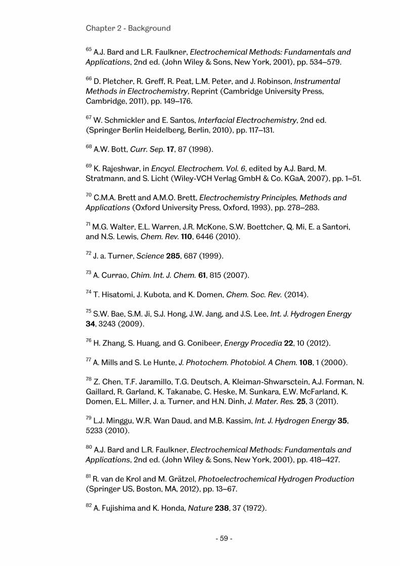
Chapter 2 - Background
- 59 -
65 A.J. Bard and L.R. Faulkner, Electrochemical Methods: Fundamentals and Applications, 2nd ed. (John Wiley & Sons, New York, 2001), pp. 534–579.
66 D. Pletcher, R. Greff, R. Peat, L.M. Peter, and J. Robinson, Instrumental Methods in Electrochemistry, Reprint (Cambridge University Press, Cambridge, 2011), pp. 149–176.
67 W. Schmickler and E. Santos, Interfacial Electrochemistry, 2nd ed. (Springer Berlin Heidelberg, Berlin, 2010), pp. 117–131.
68 A.W. Bott, Curr. Sep. 17, 87 (1998).
69 K. Rajeshwar, in Encycl. Electrochem. Vol. 6, edited by A.J. Bard, M. Stratmann, and S. Licht (Wiley-VCH Verlag GmbH & Co. KGaA, 2007), pp. 1–51.
70 C.M.A. Brett and A.M.O. Brett, Electrochemistry Principles, Methods and Applications (Oxford University Press, Oxford, 1993), pp. 278–283.
71 M.G. Walter, E.L. Warren, J.R. McKone, S.W. Boettcher, Q. Mi, E. a Santori, and N.S. Lewis, Chem. Rev. 110, 6446 (2010).
72 J. a. Turner, Science 285, 687 (1999).
73 A. Currao, Chim. Int. J. Chem. 61, 815 (2007).
74 T. Hisatomi, J. Kubota, and K. Domen, Chem. Soc. Rev. (2014).
75 S.W. Bae, S.M. Ji, S.J. Hong, J.W. Jang, and J.S. Lee, Int. J. Hydrogen Energy 34, 3243 (2009).
76 H. Zhang, S. Huang, and G. Conibeer, Energy Procedia 22, 10 (2012).
77 A. Mills and S. Le Hunte, J. Photochem. Photobiol. A Chem. 108, 1 (2000).
78 Z. Chen, T.F. Jaramillo, T.G. Deutsch, A. Kleiman-Shwarsctein, A.J. Forman, N. Gaillard, R. Garland, K. Takanabe, C. Heske, M. Sunkara, E.W. McFarland, K. Domen, E.L. Miller, J. a. Turner, and H.N. Dinh, J. Mater. Res. 25, 3 (2011).
79 L.J. Minggu, W.R. Wan Daud, and M.B. Kassim, Int. J. Hydrogen Energy 35, 5233 (2010).
80 A.J. Bard and L.R. Faulkner, Electrochemical Methods: Fundamentals and Applications, 2nd ed. (John Wiley & Sons, New York, 2001), pp. 418–427.
81 R. van de Krol and M. Grätzel, Photoelectrochemical Hydrogen Production (Springer US, Boston, MA, 2012), pp. 13–67.
82 A. Fujishima and K. Honda, Nature 238, 37 (1972).

Chapter 2 - Background
- 60 -
83 P.N. Ciesielski, F.M. Hijazi, A.M. Scott, C.J. Faulkner, L. Beard, K. Emmett, S.J. Rosenthal, D. Cliffel, and G. Kane Jennings, Bioresour. Technol. 101, 3047 (2010).
84 R.M. Navarro Yerga, M.C. Alvarez Galván, F. del Valle, J. a Villoria de la Mano, and J.L.G. Fierro, ChemSusChem 2, 471 (2009).
85 M. Woodhouse and B. a Parkinson, Chem. Soc. Rev. 38, 197 (2009).
86 M. Ni, M.K.H. Leung, D.Y.C. Leung, and K. Sumathy, Renew. Sustain. Energy Rev. 11, 401 (2007).
87 F.E. Osterloh, Chem. Soc. Rev. 42, 2294 (2013).
88 S.R. Morrison, Electrochemistry of Semiconductor and Oxidized Metal Electrodes, Illustrate (Plenum Press, New York, 1980).
89 J.D. Beach, R.T. Collins, and J. a. Turner, J. Electrochem. Soc. 150, A899 (2003).
90 P.G. Moses and C.G. Van de Walle, Appl. Phys. Lett. 96, 021908 (2010).
91 S.S. Kocha, J. Electrochem. Soc. 142, L238 (1995).
92 J.D. Beach, InxGa1-xN For Potoelectrochemical Water Splitting, Colorado School of Mines, 2001.
93 N. Kobayashi, T. Narumi, and R. Morita, Jpn. J. Appl. Phys. 44, L784 (2005).
94 K. Fujii and K. Ohkawa, Jpn. J. Appl. Phys. 44, L909 LP (2005).
95 K. Fujii, T. Karasawa, and K. Ohkawa, Jpn. J. Appl. Phys. 44, L543 (2005).
96 K. Fujii and K. Ohkawa, J. Electrochem. Soc. 153, A468 (2006).
97 Y. Iwaki, M. Ono, K. Yamaguchi, K. Kusakabe, K. Fujii, and K. Ohkawa, Phys. Stat. Sol (C) 5, 2349 (2008).
98 S.-Y. Liu, J.K. Sheu, M.L. Lee, Y.-C. Lin, S.J. Tu, F.W. Huang, and W.C. Lai, Opt. Express 20 Suppl 2, A190 (2012).
99 K. Fujii, H. Nakayama, K. Sato, T. Kato, M.-W. Cho, and T. Yao, Phys. Stat. Sol (C) 5, 2333 (2008).
100 K. Fujii, T. Ito, M. Ono, Y. Iwaki, T. Yao, and K. Ohkawa, Phys. Stat. Sol (C) 4, 2650 (2007).
101 M. Pourbaix, Atlas of Electrochemical Equilibria in Aqueous Solutions (National Association of Corrosion Engineers, 1974).

Chapter 2 - Background
- 61 -
102 D. Takagi, T. Narumi, N. Kobayashi, J. Yamamoto, Y. Ban, and K. Wakao, Jpn. J. Appl. Phys. 46, 572 (2007).
103 M. Ono, K. Fujii, T. Ito, Y. Iwaki, A. Hirako, T. Yao, and K. Ohkawa, J. Chem. Phys. 126, 054708 (2007).
104 I. Waki, D. Cohen, R. Lal, U. Mishra, S.P. DenBaars, and S. Nakamura, Appl. Phys. Lett. 91, 093519 (2007).
105 H. Jung, Y. Hong, Y. Li, J. Cho, Y. Kim, and G. Yi, ACS Nano 2, 637 (2008).
106 J.-S. Hwang, T.-Y. Liu, S. Chattopadhyay, G.-M. Hsu, A.M. Basilio, H.-W. Chen, Y.-K. Hsu, W.-H. Tu, Y.-G. Lin, K.-H. Chen, C.-C. Li, S.-B. Wang, H.-Y. Chen, and L.-C. Chen, Nanotechnology 24, 055401 (2013).
107 K. Fujii, T. Kato, K. Sato, I. Im, J. Chang, and T. Yao, Phys. Stat. Sol (C) 7, 2218 (2010).
108 J. Benton, J. Bai, and T. Wang, Appl. Phys. Lett. 102, 173905 (2013).
109 B. AlOtaibi, M. Harati, S. Fan, S. Zhao, H.P.T. Nguyen, M.G. Kibria, and Z. Mi, Nanotechnology 24, 175401 (2013).
110 B.S. Kwak, J. Kim, and M. Kang, Int. J. Hydrogen Energy 35, 11829 (2010).
111 N.V. Long, M. Ohtaki, T.D. Hien, J. Randy, and M. Nogami, Electrochim. Acta 56, 9133 (2011).
112 X. Wang, G. Liu, G.Q. Lu, and H.-M. Cheng, Int. J. Hydrogen Energy 35, 8199 (2010).
113 W.-H. Tu, Y.-K. Hsu, C.-H. Yen, C.-I. Wu, J.-S. Hwang, L.-C. Chen, and K.-H. Chen, Electrochem. Commun. 13, 530 (2011).
114 K. Ohkawa, W. Ohara, D. Uchida, and M. Deura, Jpn. J. Appl. Phys. 52, 08JH04 (2013).
115 J. Benton, J. Bai, and T. Wang, Appl. Phys. Lett. 103, 133904 (2013).
116 S.H. Kim, M. Ebaid, J.-H. Kang, and S.-W. Ryu, Appl. Surf. Sci. 305, 638 (2014).
117 K. Aryal, B.N. Pantha, J. Li, J.Y. Lin, and H.X. Jiang, Appl. Phys. Lett. 96, 052110 (2010).
118 J. Li, J.Y. Lin, and H.X. Jiang, Appl. Phys. Lett. 93, 162107 (2008).
119 M. Li, W. Luo, B. Liu, X. Zhao, Z. Li, D. Chen, T. Yu, Z. Xie, R. Zhang, and Z. Zou, Appl. Phys. Lett. 99, 112108 (2011).

Chapter 2 - Background
- 62 -
120 W. Luo, B. Liu, Z. Li, Z. Xie, D. Chen, Z. Zou, and R. Zhang, Appl. Phys. Lett. 92, 262110 (2008).
121 K. Fujii, S. Nakamura, S. Yokojima, T. Goto, T. Yao, M. Sugiyama, and Y. Nakano, J. Phys. Chem. C 115, 25165 (2011).
122 Y.J. Hwang, C.H. Wu, C. Hahn, H.E. Jeong, and P. Yang, Nano Lett. 12, 1678 (2012).
123 B. AlOtaibi, H.P.T. Nguyen, S. Zhao, M.G. Kibria, S. Fan, and Z. Mi, Nano Lett. 13, 4356 (2013).

Chapter 3 – Experimental Techniques
- 63 -
Chapter 3
Experimental Techniques
arious techniques are required to achieve the targets for the
project, including device fabrication, structural characterisation
and performance assessment. The principles behind each technique are
introduced in detail in order to provide a coherent overview of all methods
utilised.
3.1 Growth
All wafers were grown in a single chamber 3x2” showerhead metal
organic chemical vapour deposition (MOCVD) reactor. A schematic of the
reaction process is illustrated in Figure 3-1. As discussed in Chapter 2,
trimethyl-metals (Al, Ga or In) and ammonia are used as reagents with
nitrogen gas the carrier gas. A growth substrate (2” sapphire wafer) is placed
onto a susceptor, which then enters into the reaction chamber. The flow
rates of the reagents are controlled depending on reaction requirements and
the susceptor heats the substrate to the specified growth temperatures. As
the reagents (trimethy gallium and ammonia) enter the chamber, the
decomposition process initiates at the surface of the substrate, due to the
elevated temperature, and epitaxial layers begin to form. As a result of the
reaction, chemical by-products in the form of methane (CH4) are formed and
removed from the chamber by the carrier gases. The deposition process
V

Chapter 3 – Experimental Techniques
- 64 -
continues until the desired epitaxial later thicknesses are achieved and the
reaction terminated.
Figure 3-1 – Schematic illustration of reaction process in a metal organic chemical vapour deposition (MOCVD) reactor for the growth of GaN
3.2 Fabrication
A number of methods for semiconductor device fabrication have been
developed in order to fabricate novel nanostructures with an enhanced
performance within this thesis. The majority of device fabrication has been
performed in the high class cleanroom at Sheffield University, where the
EPSRC III-V National centre is partially involved. All the material
characterization and device testing has been carried out within our III-nitride
research group. All the epi-wafers utilised are also grown within our III-nitride
research group.
3.2.1 Dry Etch Techniques
Etching technologies are typical approaches for the fabrication of
semiconductor devices. There are two major approaches, dry etching and
chemical wet etching.1 The former provides a quick and isotropic etching
process however it will generally generate damage which can be avoided in
chemical etching. Depending on the materials utilised, the wet etching rate
and final surface effect can vary significantly. Alongside this, wet etching also

Chapter 3 – Experimental Techniques
- 65 -
depends on crystallographic orientation of the material. In practical
applications within the semiconductor industry, dry etching is the dominant
approach. Both dry and wet etch methods, including photoelectrochemical
wet etching are utilised to achieve the desired nanostructures.
Reactive-Ion Etching
Reactive-ion etching (RIE) utilises chemically reactive plasma to etch
semiconductors, where the plasma is generated under low pressure
(vacuum) through a radio frequency (RF) generator. It can provide a greater
degree of control over etch conditions and profiles. An RIE consists of a
process chamber in which two parallel electrodes are positioned at the top
and base of the chamber. The side walls and upper electrode are electrically
grounded, isolating the lower electrode where the sample is located. The
chamber allows for a controlled flow of etchant gases into the chamber
during the etch process.
As mentioned above, it is necessary to pump down the pressure of the
chamber prior to etching. Etchant gases are then injected into the chamber
and the pressure stabilised. Typical etchant gases include Ar, CHF3, O2, SF6
and the flow rates controlled depending on the required etch,2 usually at low
pressures of a few millitorr. CHF3, O2 and SF6 are the main gases used in this
work for the etching of SiO2.3–5 Once stabilised, a radio frequency (RF)
generator with a typical frequency of 13.56 megahertz is switched on, with a
power around 100 W, to the lower electrode creating an electric field
between the parallel electrodes. The RF electric field ionises the gas
molecules, losing electrons from their outer orbitals becoming positive ions.
This forms a high density plasma within the chamber. As a result of the
electric isolation of the lower electrode, bombardment of electrons to the
sample platter causes an electron charge to build-up. The disproportionate
charge between the upper and lower electrodes causes the positive etchant
gas ions to migrate towards the sample. These ions interact with the sample
surface where they either react or remove some of the sample material.
Hence it is the reactive-ions within the chamber that result in the etching of
the material.

Chapter 3 – Experimental Techniques
- 66 -
Inductively Coupled Plasma RIE
Inductively coupled plasma etching (ICP) is another advanced dry
etching technique which includes the RIE function. ICP has an additional
plasma generator in the form of an inductively coupled generator. The
resultant enhanced plasma density allows for a greater degree of control
over the etch conditions and results in faster etch rates. In normal RIE
systems, etch rates are limited as increasing the RF power will cause the bias
voltage across the cathode to increase, reducing the selectivity of the etch.
ICP allows for greater selectivity due to the separation of the RF generator
and etch chamber, with the RF coupled into the chamber with an inductive
couple. A second RF generator is connected to the sample stage increasing
the plasma density. The combination of the two generators gives a greater
degree of control over the self-biasing of the sample platter. ICP has been
widely used for the etching of III-nitride materials, typically with a Cl2/Ar gas
mixture.6,7 The etchant gas flow and RF power can be controlled depending
of the required etch. An Oxford Instruments Plasma Technology ICP 380 is
utilised within this thesis.
3.2.2 Photolithography
Photolithography is a standard technique in semiconductor device
processing, allowing the transfer of a pattern from prepared masks to the
material for further device fabrication process. A light sensitive material,
known as a photoresist is utilised as the medium to transfer the pattern to
the sample. As a result of the light sensitivity, device processing is performed
in a yellow room in which filters have been implemented to prevent the
premature change in the photoresists chemical makeup. The typical
conditions utilised to obtain the best uniformity are described. Prior to
deposition of the photoresist, the sample is dehydrated at 100 °C to remove
any adsorbed moisture from the surface and prevent proper adhesion of the
photoresist. The sample is then spun at 4000 rpm for 30 seconds to remove
any further dust particles. A few drops of resist are then placed upon the
sample and left to spread before spinning again at 4000 rpm to create a thin

Chapter 3 – Experimental Techniques
- 67 -
even film. It is finally soft-baked at 100 °C for a minute to remove excess
resist solvent to prevent the sample sticking to the photomask.
A photomask is a quartz plate in which a designed pattern is deposited
onto one side, commonly in chrome. The photomask is inserted into a mask
aligner with the metal side down and secured in position. The photoresist
covered sample is positioned under the photomask, aligned and moved into
contact with the metal side. An exposure time is set and the sample exposed
to UV light through the photomask, transferring the pattern onto the sample
by altering the bonds within the photoresist in the exposed areas. The
exposed sample is then developed in the resists counterpart developer,
finalising the transfer of the pattern. With a positive resist the developer
removes the exposed resist while with a negative resist the developer
removes any unexposed resist. Exposure and development times are
dependent on the resist, UV source and developer. As a final step the sample
is rinsed in deionised water to prevent any further development once the
sample is taken out of the yellow room. Multiple stages of lithography are
possible with sequential masks aligned via the use of alignment marks on the
photomask. A Karl Suss MJB3 aligner is utilised in this work.
3.2.3 Thin Film Deposition
The deposition of thin films upon semiconductors is a vital aspect of
semiconductor processing in which a variety of materials are utilised. These
materials can be either dielectric material such as SiO2 or metal contacts.
There are a variety of different techniques available to achieve the desired
result, which will be used for the project and thus be introduced below
Plasma Enhanced Chemical Vapour Deposition
A plasma enhanced chemical vapour deposition (PECVD) is based on a
technique with a mechanism which is similar to that of a reactive ion etcher in
regards to the utilisation of plasma. Within a device chamber there are two
parallel electrodes, gas inlet/outlet pipes and an RF generator.8 In
comparison to chemical vapour deposition (CVD) the introduction of the
plasma allows a reduction of the growth temperatures of the thin films.

Chapter 3 – Experimental Techniques
- 68 -
PEVCD is commonly used for the growth of dielectric materials, typically,
SiO2 or Si3N4.9 Reactant gases (SiH4, N2, N2O ) are injected into a chamber
resting at an elevated temperature (~300 °C). An RF generator is used to
create the plasma within the chamber generating a bias between the upper
and lower electrodes. The reactive gas mixture, containing radicals, ions,
atoms and molecules will then interact with the substrate surface. The
diffusion of the reactive species to the sample surface then results in a
surface reaction forming the required film.8 Specification of the conditions
within the chamber – flow rate, temperature, RF power – allows the
deposition rate to be controlled and precise growth rates can be achieved
allowing the growth of high quality thin films.10 Within this work, PECVD has
been typically utilised for the growth of silicon dioxide layers.
Thermal Evaporation
Thermal evaporation is a physical vapour deposition method widely
utilised for the deposition of a variety of metals. The material to be deposited
is fitted within the deposition chamber, typically a piece of metal wire
inserted into a tungsten filament, and the sample is located at the base of the
chamber.11 A high vacuum (~3x10⁻⁶ torr) is required for deposition in order to
significantly reduce or eliminate disruption as a result of the residual gas in
the chamber. The solid material is then heated via passing a current (~20-40
A) through the tungsten coil, melting the solid material and thus creating an
atomic vapour within the deposition chamber. Due to the directionality of
the deposition, the vapour cloud condenses on the surface of semiconductor
samples, forming a thin film on the sample.12
A crystal thickness monitor is located beneath the filament, and
employed to monitor the deposition thickness throughout the process. Films
range from a few nanometres through to micrometres and multiple materials
can be deposited in a single deposition. An Edwards E306a deposition system
is implemented in this work.

Chapter 3 – Experimental Techniques
- 69 -
E-beam Evaporation
An E-beam evaporator is another physical vapour deposition technique
operating in a similar manner to a thermal evaporator, with a highly energised
electron beam implemented instead of a resistive coil in order to generate
atomic vapour. In contrast to the thermal evaporator, the material source is
located at the base of the chamber and the samples located above the source.
Deposition material is placed into a crucible which is then inserted into the
chamber. A high vacuum is also required in this deposition process. An
electron gun, operating at about 10 kV, is fired at the crucible atomising the
deposition material.11 A crystal thickness monitor is again utilised to monitor
the deposition rate and film thickness. .
Sputter Deposition
Another physical vapour deposition technique, this involves the use of
a sputter target and deposition substrate. A high vacuum is achieved prior to
deposition and then an inert gas is fed into the system at a specified flow rate.
A current is applied between the target (cathode) and sample platter
(anode) which ionises the inert gas creating a plasma.11 The plasma impacts
the sputter target ejecting atoms into the chamber. The ejected atoms
deposit on top of the sample surface forming a thin even material layer.
Various materials are available to sputter, however it is metal films of Ti, Au
and Ni that are fabricated in this work.
3.2.5 Rapid Thermal Annealing
It is often necessary to quickly heat or cool samples during processing,
either as a fabrication step or alloy metallisation in the formation of ohmic
contacts. One method is via rapid thermal annealing (RTA) in which higher
temperatures (300-900 °C) are achieved in a matter of minutes evenly
heating the sample. The RTA operates with the use of two silicon susceptor
wafers, separated by a small air gap with the sample residing on the lower
wafer. Once entered into the chamber, the banks of infra-red bulbs are
initiated, radiatively heating the silicon wafers. The chosen gas, N2, N2/O2 mix,
is passed through the chamber. The lower wafer passes heat into the sample
while the upper wafer will radiatively heat the area above the sample. The
Chapter 3 – Experimental Techniques
- 70 -
temperature is controlled by the use of a pyrometer. Following the rapid
heating, the sample is cooled with high flowing nitrogen.
3.3 Characterisation
Assessment of the fabricated devices is an essential requirement in
semiconductor processing. There are a number of characterisation
techniques to completely assess the full performance of the device. Optical
techniques provide non-destructive feedback on the material properties,
such as information regarding the band gap or stresses in a system. Solar
hydrogen naturally involves the use of light and therefore optical
characterisation results in knowledge on the performance of a device.
3.3.1 Photoluminescence
Photoluminescence (PL) is a very powerful technique to study optical
properties of semiconductors. A PL system consists of an excitation source,
typically a laser whose energy should be high enough to excite the material
under study, a monochromator which can disperse the emission and a
proper detector which can detect the emission. For GaN whose band edge is
around 3.4 eV (or 362 nm), a 325 nm laser or any laser whose wavelength is
shorter than 362nm is utilised to allow electrons from the valence band to be
promoted into the conduction band. The schematic of a typical system is
illustrated in Figure 3-2.
Figure 3-2 – Schematic of Photoluminescence experimental set-up

Chapter 3 – Experimental Techniques
- 71 -
In quantum well samples due to the structure of the semiconductor,
excitation with a laser suitable for GaN emission will result in reduced
absorption of the InGaN quantum wells due to absorption by the GaN capping
layers. Therefore a 375 nm (or any laser >362 nm) laser is utilised, passing
through the GaN resulting in excitation of the carriers in the quantum well
only allowing the properties of these structures to be investigated.
3.3.2 Scanning Electron Microscopy
High resolution images are required in order to assess semiconductor
nanostructures. Scanning electron microscopy (SEM) works by focusing a
beam of electrons onto a sample surface producing resolutions on
nanometre scales.13 Operating within a vacuum, a steady stream of electrons
is required. A field emission gun (FEG) is utilised in this research which
operates via the formation of a strong electrical field to remove electrons
from their associated atoms. A series of magnetic lenses focuses the
electrons into an electron beam which is then centred onto the sample. The
interaction of the electron beam with the sample surface ejects secondary
electrons which are then sensed with the secondary electron detector and
the intensity is monitored. The signal is amplified and processed to produce
an image depicting the surface of the sample. The difference in contrast
ratios is dependent on the number of secondary electrons detected.
3.3.3 Atomic Force Microscopy
Atomic force microscopy (AFM) is a beneficial tool in non-destructively
assessing the sample surface, providing topographic information difficult to
obtain in other microscopy techniques. The initial AFM utilised a scanning
tunnelling microscope in tandem with a surface profiler14 and the basic
principle is still utilized in which a cantilever and feedback mechanism is used
to assess physical properties of a sample, including atomic growth steps. On
the cantilever is a minute tip, typically made from silicon. As GaN is a very
hard material, standard silicon tips can be easily damaged. Therefore, to
assess the surface of nitrides a silicon tip with a SiN coating is implemented.
As the probe scans the surface of the sample, interactions between the probe
and the sample cause deflections of the cantilever. A laser is utilised to

Chapter 3 – Experimental Techniques
- 72 -
evaluate and monitor the deflection during a scan. This happens by reflecting
the laser spot on the back of the cantilever, providing feedback during the
scan to maintain the minimum distance between the sample and surface.
Operation of the AFM can occur via contact or non-contact techniques in
which the probe tip is either above or directly on the sample.
3.4 Photoelectrochemical Techniques
Accurate characterisation of the device performance is essential to
determine areas for improvement. Within this work, a number of different
photoelectrochemical (PEC) measurement techniques were implemented in
order to obtain a variety of information regarding the working potential of the
fabricated devices.
3.4.1 PEC Cell
Figure 3-3 - Photograph of photoelectrochemical cell utilised in majority of testing
With the vast quantity of research in the area of photoelectrochemical
procedures there is an array of different PEC cells implemented in this
research.15 Initial work was conducted on a single windowed Perspex reactor
in which the working electrode (the fabricated sample) and the counter
electrode (Pt rod) were located in the same compartment. This simple
design provided a basic analysis approach for the materials.
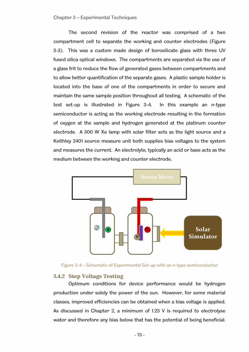
Chapter 3 – Experimental Techniques
- 73 -
The second revision of the reactor was comprised of a two
compartment cell to separate the working and counter electrodes (Figure
3-3). This was a custom made design of borosilicate glass with three UV
fused silica optical windows. The compartments are separated via the use of
a glass frit to reduce the flow of generated gases between compartments and
to allow better quantification of the separate gases. A plastic sample holder is
located into the base of one of the compartments in order to secure and
maintain the same sample position throughout all testing. A schematic of the
test set-up is illustrated in Figure 3-4. In this example an n-type
semiconductor is acting as the working electrode resulting in the formation
of oxygen at the sample and hydrogen generated at the platinum counter
electrode. A 300 W Xe lamp with solar filter acts as the light source and a
Keithley 2401 source measure unit both supplies bias voltages to the system
and measures the current. An electrolyte, typically an acid or base acts as the
medium between the working and counter electrode.
Figure 3-4 – Schematic of Experimental Set-up with an n-type semiconductor
3.4.2 Step Voltage Testing
Optimum conditions for device performance would be hydrogen
production under solely the power of the sun. However, for some material
classes, improved efficiencies can be obtained when a bias voltage is applied.
As discussed in Chapter 2, a minimum of 1.23 V is required to electrolyse
water and therefore any bias below that has the potential of being beneficial.

Chapter 3 – Experimental Techniques
- 74 -
To investigate this, with the experimental set-up described above and
demonstrated in Figure 3-4, a stepwise measurement of photocurrent under
different applied biases is tested. Biases of -1 V to 2 V in linear step
increments are supplied by the Keithley and the photocurrent measured at
each step. An illumination intensity of 100 mW cm-2 with a solar filter acts as
the light source and demonstrates the potential of the device under normal
operating conditions. The overall efficiency of the device can be calculated
via Equation 2-7.
3.4.3 Reliability Testing
Typical operating times required for these devices will be hundreds of
hours and therefore assessing the long term stability and their potential for
hydrogen production over time is essential. The test is conducted in a similar
manner to the step voltage testing however a single bias voltage is chosen and
applied for the duration of the test. The photocurrent is measured over a
prolonged period of time, taking measurements at regular intervals. Rapid
assessment of device stability is conducted with the use of increased
illumination intensity, representing an increased number of PEC cycles.
Hydrogen Monitoring
In tests in which hydrogen generation is assessed, a long term test is
conducted however the volume of hydrogen is collected. Prior to testing, the
electrolyte is purged with nitrogen to reduce any dissolved oxygen. The
platinum counter electrode is located in an upturned burette in order to
collect any gas produced. The gas (hydrogen) collects within the burette and
displaces the solution into the main cell compartment to allow monitoring
over the course of the reaction.
3.4.4 Incident Photon Conversion Efficiency
The efficiency of a device at specific wavelengths is a useful indicator
as to the operating potential of the device. The incident photon conversion
efficiency (IPCE) assesses the performance of the device under single
wavelength illumination (Equation 2-9). A 75 W Xe lamp is utilised as the light
source and a SPEX .55 monochromator allows the selection of single

Chapter 3 – Experimental Techniques
- 75 -
wavelengths. A calibrated photodiode quantifies the power density of
incident radiation. The photoelectrochemical current is measured with a
Keithley 2401. The PEC measurements were taken using the same
experimental set-up implemented for all performance testing.
3.4.5 Accuracy and Error
In order to ensure accurate results and consistent data, a number of
procedures were included to ensure a minimum degree of error. This was
achieved by keeping all test conditions identical in a set of experiments. Any
potential areas for variation were monitored and controlled to reduce error.
Within an experiment, multiple measurements were conducted and the
variation in data assessed to ensure it was within a defined tolerance level.
Consistency checks were also carried out during measurements to ensure
that all the reporting was similar to allow a comparison between
measurements. Reference samples were utilised to provide a baseline value
in which any exhibited change could effectively be assessed.

Chapter 3 – Experimental Techniques
- 76 -
Bibliography
1 B. El-Kareh, Fundamentals of Semiconductor Processing Technology, illustrate (Kluwer Academic Publishers, Massachusetts, 1994), p. 599.
2 H. Jansen, H. Gardeniers, M. De Boer, M. Elwenspoek, and J. Fluitman, J. Micromechanics Microengineering 6, 14 (1996).
3 R. Legtenberg, H. Jansen, M. De Boer, and M. Elwenspoek, 142, (1995).
4 R.F. Figueroa, S. Spiesshoefer, S.L. Burkett, and L. Schaper, J. Vac. Sci. Technol. B Microelectron. Nanom. Struct. 23, 2226 (2005).
5 S. Grigoropoulos, J. Vac. Sci. Technol. B Microelectron. Nanom. Struct. 15, 640 (1997).
6 R.J. Shul, G.B. McClellan, S. a. Casalnuovo, D.J. Rieger, S.J. Pearton, C. Constantine, C. Barratt, R.F. Karlicek, C. Tran, and M. Schurman, Appl. Phys. Lett. 69, 1119 (1996).
7 S.A. Smith, C.A. Wolden, M.D. Bremser, A.D. Hanser, R.F. Davis, and W. V Lampert, Appl. Phys. Lett. 71, 3631 (1997).
8 P.K. Chu, X. Tian, and L. Li, in Handb. Metall. Process Des., edited by G.E. Totten, K. Funatani, and L. Xie, 1st ed. (Marcel Dekker, New York, 2004), pp. 805–809.
9 S. Arulkumaran, T. Egawa, H. Ishikawa, T. Jimbo, and M. Umeno, Appl. Phys. Lett. 73, 809 (1998).
10(2003).
11 M.J. Madou, Fundamentals of Microfabrication: The Science of Miniaturization, 2nd ed. (CRC Press, Boca Raton, 2002), pp. 134–140.
12 Z. Guo and L. Tan, Fundamentals and Applications of Nanomaterials, 1st ed. (Artech House, Norwood, 2009), pp. 99–106.
13 L. Reimer, Scanning Electron Microscopy: Physics of Image Formation and Microanalysis, 2nd ed. (Springer-Verlag, New York, 1998), pp. 1–12.
14 G. Binnig, C.F. Quate, and C. Gerber, Phys. Rev. Lett. 56, 930 (1986).
15 L.J. Minggu, W.R. Wan Daud, and M.B. Kassim, Int. J. Hydrogen Energy 35, 5233 (2010).

Chapter 4 – GaN Nanostructures for Enhanced Solar Hydrogen Production
- 77 -
Chapter 4
GaN Nanostructures for Enhanced Solar
Hydrogen Production
n this chapter, a self-organised nickel mask approach developed
within the group has been used to fabricate GaN nanorod arrays for
use as photoelectrodes. A significant enhancement in solar hydrogen
generation has been achieved as a result of using a GaN-based nanorod array
in comparison with a planar one fabricated from the same parent wafer.
Under identical illumination conditions in hydrochloric acid solution, the
photoelectrode with the nanorod array structure has demonstrated a
photocurrent enhancement with a factor of 6 and an enhancement in the rate
of hydrogen generation with a factor of 7. The enhancement in solar
hydrogen generation is attributed to a massive improvement in light
absorption area, reduced travelling distance for the migration of the
photogenerated carriers to the semiconductor/electrolyte interface and
surface band bending effects.
4.1 Background
4.1.1 Nanostructures for Solar Hydrogen
The advancement of techniques for the growth and fabrication of
nanostructured semiconductors has resulted in a significant increase in the
design and implementation of these devices for water splitting.1 As discussed,
I

Chapter 4 – GaN Nanostructures for Enhanced Solar Hydrogen Production
- 78 -
water splitting is a surface reaction that requires the generation and transfer
of charge-carriers to the electrolyte. The use of nanostructures in this
process can result in improved device performance. Recombination of
photogenerated carriers is undesirable in water splitting and therefore
controlling the number of recombination centres is essential if high
efficiencies are to be achieved. The properties of the semiconductor such as
the grain size, surface morphology and number of defects all influence the
recombination pathways. As discussed, the diffusion length of the minority
carriers is a critical value if low recombination is to be obtained. Variations in
the structure of the semiconductor surface can therefore strongly influence
the recombination kinetics. As illustrated in Figure 4-1, for an identical
semiconductor material, the electrons and holes will have a specific diffusion
length, Le and Lh respectively. In a flat surface, the number of generated
carriers that will migrate to the surface is limited by the diffusion length,
reducing the active region of the device to the top layer only. If a rough
surface is employed, it is easier for the carriers to migrate to the
semiconductor-electrolyte interface due to the increase in available sites.
This increases the opportunity for reactions to occur, effectively increasing
the performance of the device.2
Figure 4-1 – Variation in charge collection in different semiconductor structures. Lh: hole diffusion length; Le: electron diffusion length. Adapted from Osterloh (2013)2
Furthermore, the use of nanostructures can increase the light
adsorption and distribution compared to flat devices.1 Light absorption is
related to the materials ability to absorb light at specific wavelengths (α) and
the Beer Lambert law. The penetration of light in a material is related to α-1

Chapter 4 – GaN Nanostructures for Enhanced Solar Hydrogen Production
- 79 -
and a film thickness of 2.3 times this coefficient is required to absorb more
than 90 % of incident light.2 Altering the structure of the semiconductor
surface can increase light absorption through scattering, reducing the loss of
light that occurs due to reflection in flat surfaces. If the total amount of light
absorbed increases, this will increase the number of carriers generated
which will improve the device performance. The increased surface area
results in a larger junction area between the semiconductor and electrolyte.
This can lead to an increase in recombination due to pathways created at
defects and trap sites, therefore careful control is required to optimise the
nanostructured design.3
Despite the underlying challenges with the use of nanostructures, their
potential is significant. Various device structures have been investigated for
water splitting including colloidal suspensions,4 nanorods,5,6 nanotubes7–9 and
branched rods.10 Varying the fabrication conditions and ultimately the
morphology of the device can and has resulted in improved device
performance.
4.1.2 GaN Nanorods
There are increasing activities on research into GaN nanostructures
for a number of applications.11,12 There are a number of approaches to the
fabrication of GaN nanostructures, mainly based on direct synthesis and
post-growth fabrication. For the former, early structures of GaN were grown
with the use of a catalyst (Au,13 Ni14 and Ta15) via the vapour-liquid-solid
growth mechanism. Horizontal growth of the nanorods occurs within a
chemical vapour deposition (CVD) system in which the catalyst particles are
dispersed on the substrate. After growth, the metal particles are found at the
tops of the nanorods. Although successful devices have been fabricated by
this technique,16 the growth can result in twisting and bunching of the
nanorods, undesirable for effective surface reactions. Alternate methods for
GaN nanostructures include catalyst free methods in which they can be
grown either via molecular beam epitaxy (MBE) or metal organic chemical
vapour deposition (MOCVD).

Chapter 4 – GaN Nanostructures for Enhanced Solar Hydrogen Production
- 80 -
Self-assembled growth techniques initially required stringent growth
conditions if nanorods were to be grown, with the III/V ratio and AlN
interlayer thickness playing crucial roles.17,18 A nitrogen rich atmosphere
produces GaN nanorods while Ga rich growth leads to thin film growth.
Nanorod density and diameter could be controlled via this technique
however the uniformity across a sample was poor. Selective area growth
(SAG) methods were investigated with the use of patterned substrates via
both MBE19 and MOCVD20 methods. Due to the control exhibited over the
patterned substrate, a high degree of uniformity was achieved via the SAG
technique and is a becoming a prevalent technology as a result of this
control.11
Post-growth fabrication techniques exhibit a number of major
advantages as MOCVD growth of standard GaN epi-wafers has been well
established. Wet and dry etch processes have been employed as post-
growth techniques for the fabrication of the nanorods.21,22 One such method
utilises nickel as an etch mask before ICP etching of the GaN occurs. This
technique creates a relatively uniform pattern on the GaN wafer.
Modifications and adaptions to this process were made to this method to
improve uniformity and quality of the etched nanorods by the nitride group at
Sheffield.23,24
GaN Nanostructures in Water Splitting
As discussed in Chapter 2, the initial focus of GaN devices were planar
structures. However there has been some limited attempts at utilising
nanorods or nanodots in this application.25,26 In both cases, the growth of the
nanostructures were via intensive processes such as e-beam lithography and
MBE growth limiting their potential for commercial III-nitride applications.
4.2 As-Grown GaN Devices
4.2.1 Fabrication
All as-grown GaN samples were grown using an MOCVD reactor. The
technique implemented has been designed by the Sheffield research group
and provides superior crystal quality compared to standard two step growth

Chapter 4 – GaN Nanostructures for Enhanced Solar Hydrogen Production
- 81 -
techniques.27,28 A high temperature (1200 °C) AlN buffer layer is grown on a
(0001) sapphire substrate under low pressure conditions after thermal
substrate cleaning in flowing hydrogen. The V/III ratio during this step is 40.
The high temperature AlN buffer layer produces an atomically flat surface as
a result of two dimensional growth dominating over the standard three
dimensional growth observed in standard techniques. This technique results
in a significant reduction in structural defects.29 An un-doped GaN layer is
then grown upon the flat AlN layer in high then low pressure conditions. The
upper active layer then follows these two procedures. For n-type GaN, silicon
is introduced as the dopant with the silane flow rate controlled to alter the
overall doping level. Magnesium is utilised as the dopant in p-type epi-wafers.
Following epi-wafer growth, the sample undergoes a number of
characterisation steps including optical microscopy and x-ray diffraction
(XRD) to assess the quality of the wafer. Samples are cleaved from the wafer
using a diamond scribing pen into regular square samples of between 0.2 cm2
and 1 cm2. Photolithographic techniques mask off a contact area of
approximately 20 % of the sample size. The ohmic contact is deposited using
either a thermal evaporator or sputterer. The contact is comprised of a
mixture of Ti/Au or Ti/Al/Ti/Au and is either 120 nm or 200 nm thick
respectively for n-type wafers. A Ni/Au contact, of approximately 60 nm, acts
as the ohmic contact to the p-type wafers. Finally an insulated copper wire is
bonded to the sample with conducting epoxy before being fully insulated with
a layer of insulating resin.
4.2.2 Device Characterisation
Assessment of the device properties were carried out with a number
of characterisation techniques including photoluminescence (PL), atomic
force microscopy (AFM) and Hall measurements.
Photoluminescence (PL)
PL measurements were conducted using a 325 nm He-Cd laser at
room temperature. The light was dispersed by a .75 M monochromator and
detected by a Jobin Yvon CCD. The observed spectrum is comprised of two

Chapter 4 – GaN Nanostructures for Enhanced Solar Hydrogen Production
- 82 -
main peaks (Figure 4-2), the near band-edge emission and a broad yellow
band emission. The near band-edge emission is centred at 361 nm, close to
the expected band gap of GaN at 300 K of 3.437 eV (360.73 nm).30 This
luminescence has been attributed to a free exciton transitions and donor-
bound excitons.31
400 600 800 1000
0.0
0.5
1.0
No
rma
lis
ed
In
ten
sit
y (
au
)
Wavelength (nm)
Yellow2.4 eV
1.08 eVAd
30 meVSi
0 eV
3.51 eVCB
VB
Figure 4-2 – Room temperature photoluminescence of silicon doped GaN (inset) schematic of donor-acceptor recombination model in n-GaN
The yellow band emission is broadly centred at 550 nm, which can be
typically observed in silicon doped GaN as a result of silicon-induced deep
levels.32,33 The emission is due to a donor-acceptor mechanism creating a
shallow and corresponding deep centre, demonstrated on inset of Figure
4-2.34 The recombination between these two donor states causes the broad
yellow band visible in silicon doped GaN and was initially identified in 1980.35
Atomic Force Microscopy (AFM)
AFM provides detailed topographic information regarding the quality
of the material surface as well as distinguishing any features such as defects,
growth steps and surface roughness. A typical surface of n-type GaN is
illustrated in Figure 4-3. In Figure 4-3 (b) the growth steps are clearly visible
despite little variation in actual height. The average surface roughness for the
as-grown wafers used in this work is typically 0.2 nm. This illustrates a good

Chapter 4 – GaN Nanostructures for Enhanced Solar Hydrogen Production
- 83 -
quality GaN sample and is attributed to the growth technique utilised,27
minimising defects within the crystal lattice.
Figure 4-3 – AFM scan of n-type GaN wafer (a) 100 µm2 surface profile (b) 3D topography of 4 µm2 scan
Hall Measurements
To assess the level of doping of the as-grown material Hall
measurements were conducted. The dopant level of n-type GaN has been
shown to have a significant effect on photocurrent36 and therefore it is a
necessary step to clarify potential device performance. Carrier
concentrations of the MOCVD grown GaN were determined via the Van der
Pauw method. This technique involves the deposition of four contacts in the
corners of a uniform piece of wafer. 5 x 5mm pieces of GaN wafer were
thoroughly cleaned by the three solvent methodology described previously,
before small pieces of indium were physically contacted to the corners of the
GaN. Vertical and horizontal voltage measurements were taken under 0.2 mA
of applied current across the different contact positions of the sample.
Measurements between the corners of the sample were also taken under the
effect of a positive and negative magnetic field. For all measurements, a 0.556
T magnet acted as the source of the field.
As a result of increased resistance at lower carrier concentrations and
increased recombination rates at higher concentrations, there is a tipping
point in which the optimum value can be attained. Figure 4-4 illustrates the
variation between carrier concentration and current density in non-biased
conditions. There is a clear trend between carrier concentration and current
even across data sets, with a potential shift around a median for different

Chapter 4 – GaN Nanostructures for Enhanced Solar Hydrogen Production
- 84 -
growth conditions. The optimum value however is approximately 2x1017 cm-3.
The shaded area illustrates the region in which the n-type GaN samples
utilised in this work fall, with carrier concentrations around 2x1018 cm-3, a
factor of 10 above the optimum value. Based on these values, the current
densities will be approximately half that under potential optimum doping
conditions.
1E16 1E17 1E18 1E190.0
0.2
0.4
0.6
0.8
Identical Conditions
Various Literature Values
Cu
rre
nt
De
nsit
y (
mA
cm
-2)
Carrier Concentraion (cm-3)
Figure 4-4 – Variation in current density with carrier concentration of different samples at 0 V bias in 1 M HCl under 150 W Xe lamp illumination, black squares
indicate samples from same test run, red circles are literature values of various tests. Shaded area indicates carrier concentration of devices used in this work. Adapted
from Ono et al.. 200736
4.2.3 Solar Hydrogen Performance
Electrochemical measurements of as-grown devices were performed
in the experimental set-up described in Chapter 3.
Preliminary Measurements
Stepwise measurements of as-grown n- and p-type GaN were
conducted in a 1 M HCl electrolyte solution under illumination and dark
conditions. Photocurrent measurements from -1 V through to 2 V were
measured in 0.2 V steps. In dark current measurements, all sources of
illumination were minimised and an equilibrium condition obtained. Multiple
measurements were taken at each step to ensure accuracy within test data.
Nominally low dark current measurements were recorded for both the n-
and p-type GaN devices (Figure 4-5). Increases in dark currents are observed
above the required potential to split the HCl electrolyte solution of 1.4 V,
consistent with expected results.

Chapter 4 – GaN Nanostructures for Enhanced Solar Hydrogen Production
- 85 -
-1 0 1 2
0.0
0.1
0.2
0.3
Cu
rre
nt
De
ns
ity
(m
A c
m-2)
Voltage (V vs VCE
)
p-GaN
n-GaN
p-GaN Dark
n-GaN Dark
Figure 4-5 – Dark and light photocurrent measurements of as-grown n- and p-type GaN devices in a 1 M HCl electrolyte solution. Illumination intenstiy was 100 mW cm-
2.
Illumination tests were conducted with a 300 W Xe lamp with a solar
filter applied. The use of a solar filter matches the output of the light source
to that of global irradiance observed at the Earth’s surface. Under these
conditions less than 2 % of the incident radiation is at wavelengths applicable
to GaN. A power density of 100 mW cm-2, corresponds to the output of one
sun and relates to approximately 2 mW cm-2 of useable radiation. Under
illumination, the turn on voltage of the n-GaN is -0.6 V and -0.4 V for p-GaN.
The difference in turn on voltage is a result of the shifted conduction and
valence band positions of the two doped materials. Under zero bias there is a
considerable difference in the obtained photocurrent of the two devices. The
n-type sample demonstrates a photocurrent 8 times higher than p-type GaN.
This result is comparative to other literature values in which the performance
of p-type GaN is significantly lower than that of n-type GaN.37 This has been
widely accepted to be a result of the higher carrier density of n-type GaN
resulting in a reduced resistance compared to the p-type GaN.
As a result of the surface reactions occurring at the interface between
the p-type GaN and electrolyte, the build-up of electrons at the surface forms
a protective barrier and prevents anodic etching of the GaN.38 This suggests
that p-type GaN could be the ideal electrode but due to material constraints
and the demonstrated photocurrent, the focus of this thesis has been on n-
type GaN and InGaN/GaN multi-quantum well (MQW) devices. As discussed
the efficiency of the device can be calculated using the following equation,

Chapter 4 – GaN Nanostructures for Enhanced Solar Hydrogen Production
- 86 -
𝜂 = 𝑗𝑝(1.23 − 𝑉𝑒𝑥𝑡)/𝐼0
Equation 4-1 – Photon to current efficiency equation of a photoelectrochemical cell under applied external bias
The calculated maximum efficiency for the devices using Equation 4-1
is 0.17 and 0.03 % for the n- and p-type devices respectively.
In order to determine the activity of the device for hydrogen
production a typical n-GaN sample is utilised. Measurements were
conducted at elevated light intensities (700 mW cm-2) and an applied bias of
0.8 V to achieve a significant volume of hydrogen in a shortened time. The
volume of hydrogen was measured via the previously discussed method. The
sample underwent 50 minutes of testing in a 0.5 M HCl solution and hydrogen
measurements were taken at periodic intervals through this time. The
theoretical value of hydrogen is obtained using the current produced during
the test (Figure 4-6(a)) and Equation 2-8). As presented in Figure 4-6(b) the
volume of hydrogen collected is very similar to the theoretical value and the
final volume is almost identical to the total possible volume. This suggests an
almost 100 % conversion rate of the photocurrent to hydrogen indicating the
potential of our n-GaN sample and device processing technique as a
photoelectrode for hydrogen production.
Figure 4-6 – Photoelectrochemical water splitting of 0.5 M HCl with n-GaN electrode under ~500 mW cm-2 and 0.8 V applied bias (a) photocurrent density (b)
Theoretical and actual hydrogen production

Chapter 4 – GaN Nanostructures for Enhanced Solar Hydrogen Production
- 87 -
Electrolytes
The role of the electrolyte is crucial in delivering high energy
conversion efficiencies as well as reducing the dissolution of the material.
The concentration and type of electrolyte plays a significant role in terms of
material viability and therefore it is important to choose a suitable electrolyte.
Ideally sea water and other water sources would be utilised due to their low
cost, abundance and chemical neutrality however due to low ion
concentration, high conversion efficiencies are required to make this a viable
option. Sea water has a typical salinity of 3.5 % equivalent to 0.6 M. The
majority of the ions are sodium and chloride however there is a variety of
other materials that make up the total. Various electrolytes are currently in
use across literature and range in pH from acidic to basic solutions.
-1 0 1 2
0.0
0.2
0.4
0.6
Cu
rre
nt
De
nsit
y (
mA
cm
-2)
Voltage (V vs VCE
)
D.I. Water
Tap Water
Sea Water
0.5 M HCl
0.5 M HNO3
0.5 M H2SO
4
0.5 M NaOH
Figure 4-7 – Photocurrent densities of n-GaN with different electrolytes under 100 mW cm-2 AM1.5 Xe lamp illumination
Photoelectrochemical measurements were conducted using a series
of n-GaN samples fabricated from the same epi-wafer. Various acidic and
basic electrolytes were tested at concentrations of 0.5 M, approximately the
level of sea water, against three water samples. De-ionised water was used as
a standard with tap water and a sample of sea water also tested. Each sample
was tested at step measurements from -1 V to 2 V under 100 mWcm-2 of
filtered illumination (Figure 4-7). As expected the deionised water
demonstrated a nominal photocurrent due to the lack of ions in the solution.
This was mirrored with the tap water in which system resistances meant the
production of photocurrent was not observed until 0.6 V vs VCE. A sample of

Chapter 4 – GaN Nanostructures for Enhanced Solar Hydrogen Production
- 88 -
sea water taken from off Sagami Bay, Japan was utilised. Due to the
increased salinity and therefore ion concentration of this sample compared
to the standard D.I. water (around 0.02 M) there is at least a 200 % increase
in photocurrent densities. Despite the increased ion concentration, the
photocurrent of sea water is still comparatively low compared to other
electrolytes. The performance in sea water does however does reach around
60 % the performance of HCl indicating the potential opportunity to utilise
sea water as the electrolyte in the future for high efficiency devices.
Table 4-1 - Reduction half reactions and potentials of 1 mol dm-3 solution under 1 atm pressure
Electrolyte Reduction Half Reaction 𝑬𝒓𝒆𝒅° (V)
Water 2𝐻2𝑂 + 4ℎ+ → 𝑂2 + 4𝐻
+ 1.23
HCl 2𝐶𝑙− + 2ℎ+ → 𝐶𝑙2 1.36
HNO3 [𝑁𝑂3]
− + 4𝐻+ + 2𝑒− → 𝐻𝑁𝑂2 +𝐻2𝑂
𝐻𝑁𝑂2 +𝐻+ + 𝑒− → 𝑁𝑂 + 𝐻2𝑂
0.93
0.98
H2SO4 2[𝑆𝑂4]2− + 2ℎ+ → [𝑆2𝑂8]
2− 2.01
NaOH 4[𝑂𝐻]− + 4ℎ+ → 𝑂2 + 2𝐻2𝑂 0.40
The choice of electrolyte can play a major role in the lifetime and
performance of the device as it can affect the products produced in the
reaction. The half reactions and reduction potentials of common electrolytes
are presented in Table 4-1. Water, hydrochloric acid, sulphuric acid and
sodium hydroxide are all potential electrolytes for the stoichiometric
production of hydrogen and oxygen. Nitric acid however, has a lower
reduction potential than water and therefore could not effectively be
identified as “water” splitting as it is not water being split. The decreased
reduction potential of the device explains the higher photocurrent obtained
in Figure 4-7. Although hydroxyl radicals have a lower reduction potential
than oxygen, the products are identical. The paired half reaction involving the
conversion of sodium ions to sodium metals requires a significantly larger
potential thereby maintaining the reaction at stoichiometric levels.
Hydrochloric acid poses a latent issue due to the similar reduction potential

Chapter 4 – GaN Nanostructures for Enhanced Solar Hydrogen Production
- 89 -
of water. In practice, losses and conversion potentials at the electrode in the
formation of oxygen result in a highly competitive reaction, resulting in the
production of both oxygen and chlorine when hydrochloric acid is
implemented as the electrolyte.
Despite the potential issues in the production of both oxygen and
chlorine, hydrochloric acid is utilised as the electrolyte for many of the
reactions reported due to the similarity to the “ideal” solution sea water.
Although sodium hydroxide or sulphuric acid appear ideal, there is evidence
to support the etching of gallium nitride or indium gallium nitride in these
solutions reducing the lifetime of the device.39 When no bias is applied, the
values for the three best electrolytes are similar indicating only minor
differences in performance can be achieved under non biased direct solar
illumination conditions.
4.2.4 Summary
The preliminary measurements indicate the potential of the material
with device efficiencies of around 0.2 % for the n-type GaN. Visible
production of hydrogen has also been demonstrated with a low level of
conversion loss between photocurrent and hydrogen generation. Therefore
modifications to the structure of the device could help to increase the overall
device performance.
4.3 GaN Nanostructured Devices
4.3.1 Fabrication
The GaN nanostructures were fabricated via the use of a self-
organised nickel nanomask that was developed in our group by Bai et al.24,40
on a typical MOCVD grown GaN wafer discussed previously. A schematic of
the fabrication process is illustrated in Figure 4-8. Initially the n-GaN wafer is
cleaned of contaminants with the described three stage solvent cleaning
process. Photolithography was utilised to mask off a contact area which is
then etched by inductively coupled plasma reactive ion etching (ICP-RIE).
The etchant gas is a mixture of Cl2 and Ar at 50 W RF power and 450 W ICP
power. The contact depth and etch time is related to the required nanorod

Chapter 4 – GaN Nanostructures for Enhanced Solar Hydrogen Production
- 90 -
size in order to allow efficient current flow from nanorod to ohmic contact.
The sample is cleaned again to remove any photoresist and 200 nm of SiO2 is
deposited via plasma enhanced chemical vapour deposition (PECVD). The
silicon dioxide is formed from SiH4 and N2O in a nitrogen atmosphere at an RF
power of 25 W and acts as an etch mask.
Figure 4-8 – Schematic of nanorod fabrication via use of self-organised nickel nanoparticles
The formation of the nickel nanoparticles follows via the deposition of
a thin nanometre thick layer of nickel on the silicon dioxide. Thermal
evaporation is the technique of choice as it provides an even layer across the
intended nanorod area. Self-organisation of the nickel occurs via a thermal
heat treatment in a rapid thermal annealer (RTA). Temperatures between
820 – 850 °C for 1 minute in a nitrogen atmosphere create a reasonably
uniform spread of nanoparticles (Figure 4-9 (a)). The thickness of nickel and
annealing conditions allow control over the nanoparticles and ultimately the
nanorod size. The nickel acts as a primary etch mask to etch through the
silicon dioxide. A reactive ion etch (RIE) using either a CHF3/SF6 or CHF3/O2
as the etchant gases produces the secondary etch mask (Figure 4-9 (b)). The
flow rates are 30:10 sccm or 35:5 sccm respectively in a 35 mbar atmosphere.

Chapter 4 – GaN Nanostructures for Enhanced Solar Hydrogen Production
- 91 -
The RF power is set at 75 W and the etch rate monitored via a laser feedback
system.
Figure 4-9 – SEM images of nanorod fabrication (a) Nickel nanoisland mask (b) Etched silicon dioxide mask (c) plan view of fabricated nanorods (d) tilted image of
finished nanorods
Prior to the second ICP etch the nickel nano-islands are removed with
a simple nitric acid treatment. The sample then undergoes the secondary ICP
etch under identical conditions to the initial etch. A hydrofluoric acid
treatment removes the silicon dioxide layer leaving the cleaned nanorods
(Figure 4-9 (c & d)). An ohmic contact of Ti/Au or Ti/Al/Ti/Au is thermally
deposited onto the contact area etched during the initial fabrication stages.
Optical investigation during the fabrication process is carried out with a
scanning electron microscope (SEM).
4.3.2 Characterisation of Nanostructures
Due to the fabrication method, a degree of control over the diameter
and height of the nanorods can be obtained. Assessing the optimum
performance of each condition can result in improved photocurrents for
solar hydrogen production. In order to determine the positive and negative
effects of the conditions, optical characterisation via SEM and PL can provide
an indication behind the effects.

Chapter 4 – GaN Nanostructures for Enhanced Solar Hydrogen Production
- 92 -
Nanorod Diameter
A degree of control over the diameter of the nanorods can be achieved
by varying the thickness of the nickel layer thermally evaporated onto the
silicon dioxide surface. As the nickel acts as the primary etch mask for the
formation of the nanorods any change in this process will result in changes to
the final etched GaN structure. The initial deposition creates a uniform layer
across the silicon dioxide surface, annealing of the nickel follows an Ostwald
ripening effect in which a decrease in the total surface energy results in the
growth of larger particles.41 As a result of the Ostwald ripening, altering the
film thickness or annealing conditions leads to a change in the size of the
formed nanoparticles.42
5 10 15 200
100
200
300
400
500
Dia
mete
r (n
m)
Nickel Thickness (nm)
Diameter
Coverage
14
16
18
20
22
24
26
28
Co
vera
ge (
%)
5 10 15 2010
8
109
NR
De
nsit
y
(NR
cm
-2)
Figure 4-10 – Relationship between nickel thickness and nanorod diameter (inset) variation in nanorod density per cm2
The original fabrication technique employed a 10 nm thick layer of
nickel resulting in diameters of approximately 200 nm.24 Varying the nickel
thickness from 2 nm to 20 nm results in a significant variation in both the
coverage of the final fabricated nanorods across the surface and the
diameter of the nanorods. Figure 4-10 illustrates the linear relationship
observed between the initial thickness and the final diameter of the nanorod.
Alongside this, the total surface coverage is also displayed. As expected, as
thickness increases the overall diameter of the nanorod increases. The
density of nanorods across the surface indicates a negative relationship
between nickel thickness and density (Figure 4-10 (inset)). With the increase

Chapter 4 – GaN Nanostructures for Enhanced Solar Hydrogen Production
- 93 -
in nickel thickness, larger nickel islands form, however the distance between
each particle is larger. These larger islands are formed by the coagulation of
the smaller islands formed initially. This process of formation is thought to be
responsible for the spread of the particle sizes (Figure 4-11).
0 200 400 600 800 1000
0.0
0.5
1.0
No
rma
lis
ed
Ab
un
da
nc
e
Nanorod Diameter (nm)
4 nm Ni
6 nm Ni
8 nm Ni
10 nm Ni
15 nm Ni
20 nm Ni
Figure 4-11 – Deviation of nanorod diameters with different nickel film thicknesses
As the size of the nickel thickness and ultimately the average size of
the particles increases, there is a general trend in which the overall spread of
the diameters increases. There is a clear broadening of the curves visible in
Figure 4-11 with particles ranging from 50 nm through to <1000 nm when a 20
nm layer of nickel is utilized as the etch mask. The non-uniformity of the
nanorods will result in various surface effects across the devices where the
bend banding and depletion region associated with the semiconductor-
electrolyte interface changes depending on diameter. Scanning electron
microscopy of the various nanorods illustrates the variation in size caused by
the deposition of different nickel thicknesses (Figure 4-12). Alongside the size
dependence, the obvious reduction in density can be noted, as described in
Figure 4-10 (inset), where the density decreases from a maximum of 2x10⁹
down to 1.2x10⁸ for the 6 nm and 20 nm nickel films respectively. As discussed,
this is a result of the coagulation of the nickel particles, resulting in a
decrease in overall nanorod numbers due to the increase in nickel thickness.

Chapter 4 – GaN Nanostructures for Enhanced Solar Hydrogen Production
- 94 -
Figure 4-12 - SEM indicating nanorod size and density of various nickel mask thicknesses (a) 4 nm (b) 6 nm (c) 8 nm (d) 10 nm (e) 15 nm (f) 20 nm
Further to this, a change in the total strain in the nanorods can be
observed via the room temperature photoluminescence (PL) of the different
nanorod diameters. The normalised PL spectrum of each device is presented
in Figure 4-13 where there is a clear increasing red shift occurring as nanorod
diameter increases. This is due to the fabrication of nanorods reducing the
compressive strain caused by the lattice mismatch that occurs between the
GaN/AlGaN and sapphire substrate.43,44 An estimation of the change in strain
can be calculated from the shift in the PL and a proportionality factor (K),
where K=21.2±3.2 meV/GPa for GaN.45 From Figure 4-13 as the size of
nanorod increases the degree of redshift and therefore reduction in
compressive strain changes. For the 4 nm–20 nm nickel masks the shift
ranges from 10 meV to 29.9 meV which relates to a change in strain of
0.47±0.08 GPa to 1.4±0.22 GPa respectively. The compressive strain present
within a GaN substrate grown on an AlN buffer layer on sapphire is
approximately 0.2 GPa for the GaN and 1.77 GPa for the AlN.45 Therefore, the
formation of the widest nanorods fabricated results in an almost complete
relaxation of the strain in the sample. It is known that the compressive strain
caused by the lattice mismatch causes the band gap of GaN to increase. This
is a result of variations in the exciton transitions caused by the differences in
the bulk material and sapphire substrate.46,47

Chapter 4 – GaN Nanostructures for Enhanced Solar Hydrogen Production
- 95 -
340 350 360 370 3800.0
0.2
0.4
0.6
0.8
1.0
No
rma
lis
ed
In
ten
sit
y (
a.u
.)Wavelength (nm)
As Grown
4 nm Ni Mask
6 nm Ni Mask
8 nm Ni Mask
10 nm Ni Mask
15 nm Ni Mask
20 nm Ni Mask
Figure 4-13 - Normalized room temperature PL of different diameter nanorods
Nanorod Height
Variation in the height of the nanorods was achieved by changing the
ICP etch time. Over time, variations in conditions within the ICP chamber
result in a degree of drifting in regards to etch rate. All samples fabricated
during the investigation on the nanorod height were conducted sequentially
allowing for direct comparison. Figure 4-14 illustrates how the etch rate
affects the nanorod height with examples of the shortest (Figure 4-14 (a))
and longest (Figure 4-14 (b)) nanorods illustrated. There is a clear trend
between etch time and nanorod height with an etch rate around 90 nm min-1.
Photoluminescence measurements of these samples were not investigated.
Figure 4-14 – (a) Variation of nanorod height with etch time (b) SEM of 1.5 minute ICP etch (c) SEM of 10 minute ICP etch
4.3.3 Solar Hydrogen Performance
An investigation into the effects of the nanorod diameter and height on
solar hydrogen performance was investigated via the standard measurement
technique described in Chapter 3.

Chapter 4 – GaN Nanostructures for Enhanced Solar Hydrogen Production
- 96 -
Nanorod Diameter
As observed, a significant degree of control over the nanorod diameter
can be achieved via the alteration of the nickel mask thickness. Utilising this
method, an optimised size for the nanorods can therefore be assessed for
solar hydrogen performance. Under the standard stepped voltage
measurement technique, with a bias from -1 V to 2 V versus the platinum
counter electrode applied, the difference in performance can be observed in
Figure 4-15. The nanorod devices all have a delayed turn-on voltage when
compared to the as-grown sample at -0.6 V compared to -0.8 V. This is
caused by surface effects of the nanorods creating an additional potential
barrier for the photogenerated electron-hole pairs to overcome and interact
with the electrolyte. As for the variation in diameter, all nanorod device
structures result in an increase in photocurrent over the reference as-grown
sample due to the increase in surface area as a result of device fabrication.48
-1 0 1 2-0.1
0.0
0.1
0.2
0.3
0.4
0.5
Cu
rren
t D
en
sit
y (
mA
cm
-2)
Voltage (V vs VCE
)
As-Grown
4 nm
8 nm
10 nm
15 nm
20 nm
Figure 4-15 - Photocurrent values for different nanorod diameters caused by varying nickel thickness
If the increase in photocurrent was purely dependent on surface area
effects then the smaller nanorods should exhibit the highest photocurrent
due the largest change in surface area. The change is surface area based on
nanorod density and average diameter is +3.47 cm2, +6.6cm2, + 2.7cm2,
+2.7cm2, +1.6cm2 and +1.7cm2 for the 4-20 nm nickel films respectively.
Therefore additional affects ultimately result in the wider (15 nm nickel film)
nanorods generating the largest photocurrent. This is in part due to the
number of effects discussed previously including the change in flux of the

Chapter 4 – GaN Nanostructures for Enhanced Solar Hydrogen Production
- 97 -
system, the light distribution and the charge transfer properties. The
minority carrier diffusion length for n-type GaN has been calculated around
250 nm.49,50 As the nanorod diameter increases so does the distance that
holes generated in the centre of the rod have to migrate. For the largest
sample, the average diameter was equivalent to twice the diffusion length. As
a result, carriers generated deep within the nanorod have a significantly
higher chance of recombination than those at the edge. Similarly, nanorods
that are smaller in diameter have decreased pathways for the holes to
migrate, decreasing recombination. From the results, the nanorods
approximately 1.5x the minority diffusion length prevent bulk like
recombination that is observed at higher diameters.
Alongside the surface area and diffusion length, the absorption
properties of the material have to be considered. A sufficient thickness of
material is required to absorb the majority of incident radiation. The light
penetration depth of GaN in which the intensity drops to 1/e of the original
value is 0.1 µm.51 In order to ensure >90 % absorbance, the film is required to
be around 0.23 µm.2 Based on these values, it is clear that until the nickel
mask thickness increases to ~10 nm, the rods are smaller than the ideal film
thickness. The combination of the light absorption, surface area and diffusion
effects provides an explanation for the variation in photocurrent observed in
Figure 4-15.
Height Optimisation
As with the diameter, control over the height is easily achievable.
Variation in the nanorod height will again alter the total surface area of the
device as well as the distances the generated carriers are expected to
migrate. Standard step-voltage measurements were conducted on the
fabricated samples (Figure 4-16). The turn-on voltage for all the nanorods are
similar as expected due to the identical diameter resulting in similar
depletion and surface effects. As with the changes to the nanorod diameter,
variation in the height will not only alter the surface area of the sample but
the recombination and light absorption effects. The optimum height for the
GaN device is between 500-800 nm with a similar performance observed for

Chapter 4 – GaN Nanostructures for Enhanced Solar Hydrogen Production
- 98 -
the three samples fabricated in this range. This is attributed to the increase
in light scattering resulting in a greater number of charge carriers being
generated.
-1 0 1
0.0
0.2
0.4
0.6
0.8
1.0
Cu
rren
t D
en
sit
y
(mA
cm
-2)
Voltage (V vs VCE
)
150 nm
300 nm
520 nm
660 nm
850 nm
1000 nm
Figure 4-16 – Variation in etch depth of GaN nanorods
As the size of the nanorod increases, the contribution of the bulk
material to the photocurrent decreases due to the variations in flux. Figure 4-
17 illustrates how flux changes as the nanorod height increases. For the
larger sample, the penetration of the light, omitting scattering effects, is only
at the tops of the nanorods and the flux of the sample is lower per unit area.
Changes in flux leads to variations in the open circuit voltage of a cell which
will ultimately impact on the thermodynamic driving force of water splitting.2
This partially explains the decrease observed in the larger nanorods. Other
factors include recombination effects. As the size of the nanorod increases
total surface area increases which can also result in an increase in the
number of defects at the surface. As the etch depth increases, there is a
greater chance for crystal defects to permeate the surface creating
recombination centres. The increased recombination will ultimately reduce
the available carriers for surface reactions decreasing the photocurrent. The
optimum conditions balance all effects, combining a high active surface area
with lower defect densities and adequate flux to provide a maximum value. It
is postulated that the low photocurrent observed for the 300 nm device is
due to the dominance of recombination effects over the positive benefits
observed from changes to the device structure.

Chapter 4 – GaN Nanostructures for Enhanced Solar Hydrogen Production
- 99 -
Figure 4-17 – Changes in absorbed flux of different nanorods (a) 150 nm nanorods (b) 1000 nm nanorods
4.3.4 Summary
The fabrication of a nanorod device structure has demonstrated
significant benefits in terms of photocurrent compared to the as-grown
device. The method of fabrication is relatively simple and includes an easy
process to control both the diameter and height of the nanorods. Optimising
these conditions has resulted in an increase in device efficiencies from 0.2 %
up to 0.46 % illustrating the potential of GaN nanorods.
4.4 InGaN/GaN in Water Splitting
The work on InGaN/GaN devices is limited with only a small number of
research groups utilising this material. The initial work by Beach52 identified
the potential of the material and following that, the majority of work has been
completed on bulk InGaN/GaN films. The performance of these films has
generally been relatively poor.53–55 Recently the use of InGaN nanodots and
MBE grown InGaN nanowires have shown some promise56,57 however as
previously discussed the commercial viability of this technique is not ideal.
Previous work on InGaN/GaN quantum wells demonstrated a slight
enhancement over bulk GaN with some variation between samples of
different quantum well barrier heights.58 Investigations into MQW
nanostructures have not previously been investigated.
4.4.1 Fabrication of InGaN/GaN MQW Devices
The epi-wafer used was grown on c-plane sapphire substrates via a
standard metal organic chemical vapour deposition (MOCVD) technique. The
wafer has a typical optical device structure (Figure 4-18), which consists of 1.4

Chapter 4 – GaN Nanostructures for Enhanced Solar Hydrogen Production
- 100 -
µm undoped GaN buffer, followed by 2.8 µm silicon doped GaN (n-GaN), a
thin In0.05Ga0.95N strain released layer and 10 periods of InGaN/GaN (2.5
nm/13.4 nm) multiple quantum wells (MQWs). A typical AlGaN layer of ~20nm
was used as an electron blocking layer (EBL). The sample was finally capped
with 200nm of magnesium doped GaN (p-GaN). This is a typical LED device
structure and therefore the fabrication described is applicable to a large
array of commercially available wafers. As-grown and nanorod devices were
fabricated via the method described in Figure 4-8 resulting in two distinct
samples.
Figure 4-18 – Structure of InGaN/GaN MQW wafer
4.4.2 Characterisation
Optical characterisation of the samples was conducted via PL and SEM
analysis (Figure 4-19). Photoluminescence measurements were carried out
at room temperature with the use of a 375 nm diode laser. From Figure 4-19
(a) a clear peak at 467 nm is observable for the as-grown device which
corresponds to a band gap of 2.66 eV, which is approximately a 16% indium
composition. This shift in wavelength increases the amount of available
energy by a factor of 4 compared to the GaN band gap. Typically, the
fabrication of nanorods results in an enhancement in the PL emission40 due
to the increase in internal quantum efficiency, surface area and a reduction in
total internal reflection. Furthermore, as observed in the GaN nanorods, the
nanorod structure provides strain relief to the wafer. As previously
discussed, a piezoelectric field exists within the InGaN/GaN quantum well

Chapter 4 – GaN Nanostructures for Enhanced Solar Hydrogen Production
- 101 -
structures due to strain, creating a red shift of the emission peak. The
observed blue shift of the nanorod structure illustrates that strain within the
device has been relaxed.24 SEM investigation (Figure 4-19 (b)) illustrates the
uniformity and structure of the fabricated nanorods. The nanorods had a
height of 700 nm, a diameter of 200 nm and a density of 6x108 cm2. This
provides an additional 2.75 cm2 per cm2 of active surface compared to the as-
grown structure.
Figure 4-19 – Characterisation of InGaN/GaN MQW samples (a) normalised room temperature PL measurements of as-grown and nanorod devices (b) SEM image of
fabricated nanorods
4.4.3 Solar Hydrogen Performance
Photocurrent and hydrogen measurements were conducted on the
planar as-grown structure and nanorod devices. Step-voltage measurements
were conducted at 100 mW cm-2 of solar illumination in a 0.5 M HCl
electrolyte solution. The obtained photocurrents for the two devices are
demonstrated in Figure 4-20. Dark photocurrent measurements were
conducted with the absence of illumination in a darkened room. Both of the
fabricated devices demonstrate low dark current measurements indicating
good insulation of the contact and minimum leakage measurements. The
obtained photocurrent of the planar as-grown device is comparable to the
literature value obtained for a MQW sample operating in similar, but
unfiltered illumination conditions.58 The device performs relatively poorly
due to the high resistance exhibited in the sample and the localisation of the
carriers. Due to the quantum well structure and the GaN barriers, the
photogenerated carriers in the quantum wells face a potential barrier to

Chapter 4 – GaN Nanostructures for Enhanced Solar Hydrogen Production
- 102 -
escape the well resulting in recombination of the carriers and hence low
conduction values.
-1 0 1 2-0.1
0.0
0.1
0.2
0.3
0.4
0.5
Ph
oto
cu
rre
nt
(mA
cm
-2)
Voltage (V vs VCE
)
As-Grown Dark
Nanorods Dark
As-Grown Illuminated
Nanorods Illuminated
Figure 4-20 – Photocurrent of as-grown and nanorod photoelectrodes as a function of bias under 100 mW cm-2 illumination and "dark" conditions
The fabrication of the nanorod structure has demonstrated a
significant enhancement over the as-grown device after turn on at -0.6 V. At
zero bias the enhancement is proportional to the increase in surface area
with an enhancement factor >3. As the applied voltage increases the
improved photocurrent exhibited from the nanorod device increases further
to a maximum enhancement of 6x at 1.0 V. The photocurrent of the nanorods
decreases at voltages around the redox potential of water (1.23 V) which has
been attributed to the decomposition of the nanorods due to
photocorrosion.26 An enhancement of 6x cannot solely be attributed to the
increase in surface area (3.75 x). The fabrication of the nanorod increases
the contact area of the device with the electrolyte which results in exposure
of the quantum wells. The diffusion length of InGaN has been reported to be
as short as 50 nm,49,59 therefore with nanorods of 200 nm in diameter this
allows for an increase in the extraction of carriers compared to the planar
device. Additionally, surface band bending as a result of the nanorod
fabrication60 enhances the separation of the photogenerated electron-hole
pairs increasing the recombination lifetime. These factors contribute to the
increased current density. The efficiency of the devices at the maximum
photocurrent value of 0.8 V are 0.042 % and 0.26 % for the as-grown and
nanorod device respectively.

Chapter 4 – GaN Nanostructures for Enhanced Solar Hydrogen Production
- 103 -
0 15 30 450.0
0.4
0.8
1.2
1.6
2.0
(b)
As-Grown
Nanorod
Cu
rre
nt
De
nsit
y (
mA
cm
-2)
Time (minutes)
(a)
0 15 30 45
0.0
0.1
0.2
0.3
0.4 As-Grown
Nanorods
As-Grown Theoretical
Nanorod Theoretical
Hy
dro
ge
n V
olu
me
(m
l)
Time (minutes)
Figure 4-21 – Photoelectrochemical measurements under 400 mW cm-2 illumination and 0.8 V bias (a) photocurrents of the as-grown and nanorod sample as a function of time (b) obtained and theoretical hydrogen measurements as a function of time
The stability and potential of the nanorod devices for hydrogen
generation were evaluated at elevated powers of 400 mW cm-2 illumination
intensity and 0.8 V (Figure 4-21). Photocurrent was measured for a 50 minute
period and hydrogen collected via the use of an upturned burette over the
platinum electrode. A reduction in photocurrent is observed in both the as-
grown and nanorod structures over the course of the 50 minute test duration
of 3.5 and 9.5 % decrease respectively. This is a reasonable performance
compared to other InGaN photoelectrodes.61,62 Despite the increased loss of
the nanorod structure, this is comparatively less than the planar structure
based on total exposed surface area in which a reduction of 13 % would be
expected. Evaluation of the hydrogen evolution potential (Figure 4-21 (b))
demonstrates a good agreement with the disparities in photocurrent of the
two devices with the nanorod structure performing significantly better than
the as-grown.
Hydrogen generation rates of 0.73 ml h-1cm-2 and 0.1 ml h-1cm-2 were
obtained for the nanorod and as-grown devices respectively. The nanorod
structure demonstrates a very good faradaic efficiency with the experimental
values similar to the theoretical values obtained from the photocurrent. This
is attributed to an increase in the surface area of the nanorod device which
allows for an increase in reactions. As discussed the nanorod structure can
also increase the number of defects at the surface creating hole traps which
can help to facilitate the reaction with the electrolyte. Comparatively, the as-

Chapter 4 – GaN Nanostructures for Enhanced Solar Hydrogen Production
- 104 -
grown device has a relatively poor efficiency. This is likely due to the
structure of the device (Figure 4-18) which is inhibiting surface reactions.
4.4.4 Summary
In this work I have demonstrated that InGaN/GaN MQW wafers can be
utilised as photoelectrodes for water splitting. Through the simple
fabrication of a nanorod array structure the photocurrent of the device has
been increased by a factor of 6 over the planar device. The enhancement is
attributed in part to the additional surface area obtained from the nanorods
increasing the number of surface reactions and light absorption area.
Furthermore, the distance required for carrier extraction has been reduced
increasing the number of electron-hole pairs contributing to the
photocurrent due to reduced recombination rates. Finally, the band bending
occurring within the nanorod aids the separation of the electrons and holes.
The efficiency of the device has been increased from 0.04 % to 0.26 % and
the rate of hydrogen generation increased by a factor of 7 while the relative
stability of the device has increased.
4.5 Conclusions
In this chapter the fabrication of a nanorod array structure via the use
of a self-organised nickel mask has demonstrated a remarkable enhancement
in the performance of GaN and InGaN photoelectrodes. A high level of
control over the structure has been demonstrated illustrating the ease in
which structural characteristics can be varied leading to optimised
performances. The enhancement exhibited by the nanorod structure is the
result of a number of factors including surface area, light absorption and
carrier diffusion. Furthermore, the use of this technique on a MQW structure
illustrates the potential to extend the absorption range of the devices to
increase the total available energy available for water splitting. A reasonable
level of stability has been demonstrated however with the increased reaction
area, anodic corrosion of the nanorod structure is an area for consideration.

Chapter 4 – GaN Nanostructures for Enhanced Solar Hydrogen Production
- 105 -
Bibliography
1 J. Zhu and M. Zäch, Curr. Opin. Colloid Interface Sci. 14, 260 (2009).
2 F.E. Osterloh, Chem. Soc. Rev. 42, 2294 (2013).
3 R.M. Navarro Yerga, M.C. Alvarez Galván, F. del Valle, J. a Villoria de la Mano, and J.L.G. Fierro, ChemSusChem 2, 471 (2009).
4 J.P. Best and D.E. Dunstan, Int. J. Hydrogen Energy 34, 7562 (2009).
5 X. Wang, G. Liu, Z.-G. Chen, F. Li, G.Q. (Max) Lu, and H.-M. Cheng, Electrochem. Commun. 11, 1174 (2009).
6 X. Wang, G. Liu, G.Q. Lu, and H.-M. Cheng, Int. J. Hydrogen Energy 35, 8199 (2010).
7 G.K. Mor, K. Shankar, M. Paulose, O.K. Varghese, and C. a Grimes, Nano Lett. 6, 215 (2006).
8 J.H. Park, S. Kim, and A.J. Bard, Nano Lett. 6, 24 (2006).
9 Z. Liu, B. Pesic, K.S. Raja, R.R. Rangaraju, and M. Misra, Int. J. Hydrogen Energy 34, 3250 (2009).
10 K. Sun, Y. Jing, C. Li, X. Zhang, R. Aguinaldo, A. Kargar, K. Madsen, K. Banu, Y. Zhou, Y. Bando, Z. Liu, and D. Wang, Nanoscale 4, 1515 (2012).
11 S. Li and A. Waag, J. Appl. Phys. 111, 071101 (2012).
12 Y.B. Tang, Z.H. Chen, H.S. Song, C.S. Lee, H.T. Cong, H.M. Cheng, W.J. Zhang, I. Bello, and S.T. Lee, Nano Lett. 8, 4191 (2008).
13 Y.-B. Tang, X.-H. Bo, C.-S. Lee, H.-T. Cong, H.-M. Cheng, Z.-H. Chen, W.-J. Zhang, I. Bello, and S.-T. Lee, Adv. Funct. Mater. 18, 3515 (2008).
14 Q. Li and G.T. Wang, Appl. Phys. Lett. 93, 043119 (2008).
15 F. Shi, H. Li, and C. Xue, J. Mater. Sci. Mater. Electron. 21, 1249 (2010).
16 F. Qian, Y. Li, S. Gradec, and C.M. Lieber, 20 (2004).
17 R. Calarco, R.J. Meijers, R.K. Debnath, T. Stoica, E. Sutter, and H. Lüth, Nano Lett. 7, 2248 (2007).
18 K.A. Bertness, A. Roshko, L.M. Mansfield, T.E. Harvey, and N.A. Sanford, J. Cryst. Growth 300, 94 (2007).

Chapter 4 – GaN Nanostructures for Enhanced Solar Hydrogen Production
- 106 -
19 E. Calleja, J. Ristić, S. Fernández-Garrido, L. Cerutti, M.A. Sánchez-García, J. Grandal, A. Trampert, U. Jahn, G. Sánchez, A. Griol, and B. Sánchez, Phys. Stat. Sol (B) 244, 2816 (2007).
20 S. Li, S. Fündling, Ü. Sökmen, R. Neumann, S. Merzsch, P. Hinze, T. Weimann, U. Jahn, A. Trampert, H. Riechert, E. Peiner, H.-H. Wehmann, and A. Waag, Phys. Stat. Sol (C) 7, 2224 (2010).
21 C.H. Chiu, T.C. Lu, H.W. Huang, C.F. Lai, C.C. Kao, J.T. Chu, C.C. Yu, H.C. Kuo, S.C. Wang, C.F. Lin, and T.H. Hsueh, Nanotechnology 18, 445201 (2007).
22 Y. Wu, C. Chiu, C. Chang, S. Member, and A. In, IEEE J. Sel. Top. Quantum Electron. 15, 1226 (2009).
23 T. Wang, GB2487917 (2011).
24 Q. Wang, J. Bai, Y.P. Gong, and T. Wang, J. Phys. D. Appl. Phys. 44, 395102 (2011).
25 H. Jung, Y. Hong, Y. Li, J. Cho, Y. Kim, and G. Yi, ACS Nano 2, 637 (2008).
26 K. Fujii, T. Kato, K. Sato, I. Im, J. Chang, and T. Yao, Phys. Stat. Sol (C) 7, 2218 (2010).
27 J. Bai, T. Wang, P. Comming, P.J. Parbrook, J.P.R. David, and a. G. Cullis, J. Appl. Phys. 99, 023513 (2006).
28 J. Bai, T. Wang, P.J. Parbrook, K.B. Lee, and a. G. Cullis, J. Cryst. Growth 282, 290 (2005).
29 J. Bai, T. Wang, P.J. Parbrook, I.M. Ross, and a. G. Cullis, J. Cryst. Growth 289, 63 (2006).
30 B. Monemar, Phys. Rev. B 10, 676 (1974).
31 D. Miller, Gallium Nitride Epitaxy by a Novel Hybrid VPE Technique, Stanford University, 2011.
32 W. Grieshaber, E.F. Schubert, I.D. Goepfert, R.F. Karlicek, M.J. Schurman, and C. Tran, J. Appl. Phys. 80, 4615 (1996).
33 E.F. Schubert, I.D. Goepfert, W. Grieshaber, and J.M. Redwing, Appl. Phys. Lett. 71, 921 (1997).
34 U. Kaufmann, M. Kunzer, H. Obloh, M. Maier, C. Manz, a. Ramakrishnan, and B. Santic, Phys. Rev. B 59, 5561 (1999).
35 T. Ogino and M. Aoki, Jpn. J. Appl. Phys. 19, 2395 (1980).

Chapter 4 – GaN Nanostructures for Enhanced Solar Hydrogen Production
- 107 -
36 M. Ono, K. Fujii, T. Ito, Y. Iwaki, A. Hirako, T. Yao, and K. Ohkawa, J. Chem. Phys. 126, 054708 (2007).
37 K. Fujii and K. Ohkawa, J. Electrochem. Soc. 153, A468 (2006).
38 K. Fujii and K. Ohkawa, Jpn. J. Appl. Phys. 44, L909 LP (2005).
39 K. Fujii, T. Karasawa, and K. Ohkawa, Jpn. J. Appl. Phys. 44, L543 (2005).
40 J. Bai, Q. Wang, and T. Wang, Phys. Stat. Sol (A) 209, 477 (2012).
41 A. Baldan, 7, 2171 (2002).
42 J.D. Carey, L.L. Ong, and S.R.P. Silva, Nanotechnology 14, 1223 (2003).
43 F. Demangeot, J. Gleize, J. Frandon, M. a. Renucci, M. Kuball, D. Peyrade, L. Manin-Ferlazzo, Y. Chen, and N. Grandjean, J. Appl. Phys. 91, 2866 (2002).
44 Y.D. Wang, S.J. Chua, S. Tripathy, M.S. Sander, P. Chen, and C.G. Fonstad, Appl. Phys. Lett. 86, 071917 (2005).
45 D.G. Zhao, S.J. Xu, M.H. Xie, S.Y. Tong, and H. Yang, Appl. Phys. Lett. 83, 677 (2003).
46 C.P. Kuo, S.K. Vong, R.M. Cohen, and G.B. Stringfellow, J. Appl. Phys. 57, 5428 (1985).
47 W. Shan, R. Hauenstein, A. Fischer, J. Song, W. Perry, M. Bremser, R. Davis, and B. Goldenberg, Phys. Rev. B. Condens. Matter 54, 13460 (1996).
48 I. Waki, D. Cohen, R. Lal, U. Mishra, S.P. DenBaars, and S. Nakamura, Appl. Phys. Lett. 91, 093519 (2007).
49 M. Godlewski, E. Łusakowska, E.. Goldys, M.. Phillips, T. Böttcher, S. Figge, D. Hommel, P. Prystawko, M. Leszczynski, I. Grzegory, and S. Porowski, Appl. Surf. Sci. 223, 294 (2004).
50 P.M. Bridger, E.C. Piquette, T.C. Mcgill, and Z.Z. Bandic, Solid State Commun. 44, 221 (2000).
51 X. Zhang, P. Kung, D. Walker, J. Piotrowski, a. Rogalski, a. Saxler, and M. Razeghi, Appl. Phys. Lett. 67, 2028 (1995).
52 J.D. Beach, InxGa1-xN For Potoelectrochemical Water Splitting, Colorado School of Mines, 2001.
53 C. Mauder, Ö. Tuna, B. Gutrath, V. Balmes, H. Behmenburg, M. V. Rzheutskii, E. V. Lutsenko, G.P. Yablonskii, M. Noyong, U. Simon, M. Heuken, H. Kalisch, and a. Vescan, Phys. Stat. Sol (C) 9, 964 (2012).

Chapter 4 – GaN Nanostructures for Enhanced Solar Hydrogen Production
- 108 -
54 J. Li, J.Y. Lin, and H.X. Jiang, Appl. Phys. Lett. 93, 162107 (2008).
55 C. Pendyala, J.B. Jasinski, J.H. Kim, V.K. Vendra, S. Lisenkov, M. Menon, and M.K. Sunkara, Nanoscale 4, 6269 (2012).
56 L. Wang, W. Zhao, Z.-B. Hao, and Y. Luo, Chinese Phys. Lett. 28, 057301 (2011).
57 B. AlOtaibi, H.P.T. Nguyen, S. Zhao, M.G. Kibria, S. Fan, and Z. Mi, Nano Lett. 13, 4356 (2013).
58 K. Fujii, S. Nakamura, S. Yokojima, T. Goto, T. Yao, M. Sugiyama, and Y. Nakano, J. Phys. Chem. C 115, 25165 (2011).
59 L. a. Vilbois, a. Cheknane, a. Bensaoula, C. Boney, and T. Benouaz, Energy Procedia 18, 795 (2012).
60 R.-S. Chen, H.-Y. Chen, C.-Y. Lu, K.-H. Chen, C.-P. Chen, L.-C. Chen, and Y.-J. Yang, Appl. Phys. Lett. 91, 223106 (2007).
61 M. Li, W. Luo, B. Liu, X. Zhao, Z. Li, D. Chen, T. Yu, Z. Xie, R. Zhang, and Z. Zou, Appl. Phys. Lett. 99, 112108 (2011).
62 K. Aryal, B.N. Pantha, J. Li, J.Y. Lin, and H.X. Jiang, Appl. Phys. Lett. 96, 052110 (2010).

Chapter 5 – NiO Nanoparticles on GaN Nanorods for Reduced Etching
- 109 -
Chapter 5
NiO Nanoparticles on GaN Nanorods for
Reduced Etching
omplementary materials have been added to various material
systems for solar hydrogen production with the aim being to
either increase photocurrent or hydrogen evolution rate. In this chapter, by
means of depositing transparent nickel oxide nano-particles on the nanorod
array structure, a significant reduction in photo-electrochemical etching
effects has been achieved on an InGaN/GaN nanorod array structure used as
a photoelectrode in a NaOH electrolyte. In the meantime, the addition of the
nickel oxide nano-particles has also led to an increase in photocurrent, thus
enhancing the energy conversion efficiency. The mechanisms for the
enhanced photocurrent and minimising the photochemical etching effect of
GaN in NaOH have been systematically investigated.
5.1 Cocatalysts in Water Splitting
In order to improve the efficiency of photocatalysis the addition of
cocatalysts has become a relatively common practice.1 Due to noble metals
(Pt, Pd) demonstrating a high level of activity for hydrogen reduction, the
inclusion on the surface of other photocatalysts (TiO2, Fe2O3) can increase
the overall hydrogen generation rate. Cocatalysts provide reaction sites and
decrease the activation energy for gas generation.2 Traditionally noble metals
C

Chapter 5 – NiO Nanoparticles on GaN Nanorods for Reduced Etching
- 110 -
(Pt, Rh) are utilised due to their high reaction rates in promoting the H2
evolution reaction.3 These cocatalysts are typically added to metal oxide
photocatalysts as a result of their insufficient conduction band position.
Noble metals also catalyse the reverse reaction, forming water from the
generated hydrogen and oxygen. As a result of this there is a limit as to their
potential in water splitting. In order to prevent this competitive reaction
occurring a core/shell structure is commonly utilised (Figure 5-1). The design
of the structure allows the promotion of the hydrogen reaction at the
noble/metal core with an effective transfer of electrons. The shell prevents
the penetration of oxygen to the core, effectively minimising the formation of
water. As with the standard formation of hydrogen, the reaction proceeds via
a number of steps. Initially hydrogen ions permeate the shell and adsorb
onto the core. A transfer of electrons between the photoelectrode material
and core metal occurs prior to the reduction of the hydrogen ions at the
metal core surface. Due to the close proximity of multiple individual
hydrogen ions on the core surface, adhered molecular hydrogen is formed.
Finally desorption occurs releasing gaseous molecular hydrogen as
demonstrated in Figure 5-1.
Figure 5-1 – Illustration of hydrogen and oxygen evolution on a core/shell structure on a bulk photoelectrode material. Adapted from Maeda, 2010.2
Detailed studies have been confirmed that without the core/shell
structure the evolution of gases is prevented due to the effective backward
reaction caused by the noble metal cocatalysts.4 The cocatalyst used is

Chapter 5 – NiO Nanoparticles on GaN Nanorods for Reduced Etching
- 111 -
dependent on the bulk photocatalyst with Pt showing a good performance in
sulphide based devices.5 For oxide photocatalysis, common materials include
Rh or NiOx materials. A recent review by Kuda illustrates the various
cocatalysts used on different photocatalysts.3 The NiOx cocatalyst is formed
from a nickel core with a nickel oxide shell and is utilised for the promotion of
the hydrogen reaction as illustrated in Figure 5-1.6,7
Another function of cocatalysts is to engineer band structures in order
to enhance carrier transfer (Figure 5-2). Wide band gap semiconductors, for
example GaN, have the correct band structures to straddle the two redox
levels of water. Loading the material with a complementary cocatalyst can
enhance the electron transfer from the wide band gap semiconductor
conduction band into the conduction band of the cocatalyst promoting the
hydrogen reaction at this site. This has been demonstrated in various
tanatalate systems.3,8
Figure 5-2 - Band structures of wide band gap semiconductor (i) and cocatalyst (ii)
Control over the deposition procedure and method is required in
order to achieve the desired enhancement. The approaches to the
deposition of cocatalysts include photodeposition (PD) and impregnation
techniques. Photodeposition involves the use of selective chemical solutions
and an irradiation source. As a result of the use of an irradiation source there
is some selectivity regarding the position of the deposited cocatalysts.9,10
Impregnation involves the chemical deposition of a solution onto the

Chapter 5 – NiO Nanoparticles on GaN Nanorods for Reduced Etching
- 112 -
photocatalyst followed by calcination of the cocatalyst. As a result the
particles are more randomly dispersed over the surface over the main
photoelectrode. Changing the loading of the catalyst can alter the overall
effectiveness of the device.11 It is therefore important to obtain proper
deposition techniques in order to effectively enhance device performance.
5.1.1 Cocatalysts on GaN
Despite the widely accepted requirement of cocatalysts for effective
water splitting the research into materials complementary to GaN is limited.
Wang et al. photodeposited a ruthenium and chromium oxide core/shell
structure onto MBE grown GaN nanowires.12 The core/shell structure aided
the overall photocatalytic reaction on the GaN nanowires in pure water
increasing the activity of the device. Stable evolution of stoichiometric
amounts of hydrogen and oxygen for 18 hours has been achieved. In addition
to Rh/Cr2O3 structure, the deposition of NiO on GaN has increased the
stability of the device.13 Ohkawa et.al proposed that NiO could lead to the
oxidation reaction occurring at the interface between NiO and electrolyte
instead of the GaN/electrolyte interface. This resulted in a stable
photocurrent for 500 hours indicating the significant reduction in the
corrosion of GaN in hydroxide solutions. However, further study into the
mechanism is necessary. In this chapter, a significant improvement in the
performance of GaN based devices is observed with the utilisation of NiO
nanoparticles deposited on GaN in terms of efficiency and minimising
corrosion. After our report on the utilisation of NiO nanoparticles on GaN
nanostructures, another group has also employed NiO nanoparticles on
planar GaN and achieved excellent results, further supporting the current
findings of this thesis.14
5.2 GaN/InGaN Devices
In order to effectively assess the optimum technique for the
fabrication of NiO nanoparticles on GaN based devices initial tests were
conducted on planar and nanorod n-type GaN. As illustrated in Figure 2-16,
there are many semiconductors that have the proper band structure, which

Chapter 5 – NiO Nanoparticles on GaN Nanorods for Reduced Etching
- 113 -
can straddle the two redox levels for water splitting. Ideally for a multi
semiconductor device the second semiconductor would be of a smaller band
gap to increase the amount of visible light available. If this is the case, then
the conduction and valence band positions of the semiconductors have to be
in a suitable position to allow effective charge transfer. As discussed,
cocatalysts can aid the hydrogen evolution reaction promoting electron
transfer to the cocatalyst. Alternatively the cocatalyst can aid the separation
of the photogenerated carriers. The use of NiO promotes the latter function
due to the positions of the conduction and valence bands compared to GaN
(Figure 5-3). As the band gap of NiO is larger than that of GaN, it doesn’t
provide any sensitization however is transparent to the wavelengths required
to promote carriers in GaN. This allows both semiconductors to become
active upon irradiation.
Figure 5-3 – Relative conduction and valence band positions of NiO and GaN based semiconductors
5.2.1 Fabrication
A typical n-type GaN wafer described in Chapter 4 and three
InGaN/GaN MQW wafers of different indium contents were utilised. For the
n-type GaN a high temperature (1200 °C) AlN buffer layer is grown on a
(0001) sapphire substrate under low pressure conditions after thermal
substrate cleaning in flowing hydrogen. An un-doped GaN layer is then grown

Chapter 5 – NiO Nanoparticles on GaN Nanorods for Reduced Etching
- 114 -
upon the flat AlN layer. Following this an n-type GaN layer of ~1.5 µm is grown
via the introduction of di-silane to the MOCVD reactor. GaN nanorods were
also fabricated via the same method identified in Chapter 4 in which a two
stage etch mask is utilised to fabricate controlled nanorods via inductively
coupled plasma etching. For the InGaN/GaN MQW wafers the structure is
similar to that used in the initial nanorod study described in Chapter 4.
Essentially a 1.4 µm undoped GaN buffer, followed by 2.8 µm silicon doped
GaN (n-GaN) is grown on a c-plane sapphire substrate. Following this a thin
In0.05Ga0.95N strain release layer and 10 periods of InGaN/GaN (2.5 nm/13.4
nm) multiple quantum wells (MQWs) are grown. A typical AlGaN layer of
~20nm was used as an electron blocking layer (EBL) before being finally
capped with 200nm of magnesium doped GaN (p-GaN). Nanorods were
fabricated by the method previously described in Chapter 4.
Figure 5-4 – Examples of NiO fabrication (a) after nickel deposition (b) after annealing
The preparation of the NiO nano-particle films on the samples is then
performed. Initially the contact area of the sample is masked off via standard
photolithographic techniques. Following this a thin layer of nickel (2-8 nm) is
deposited onto the surface of the sample via a standard thermal evaporation
approach. The samples then undergo an annealing process at 850 °C for 1
minute in a nitrogen atmosphere in order to form self-organised Ni
nanoparticles. This technique is similar to that used in the formation of the
nickel nanomasks developed by our group for the nanorod fabrication. The
major difference between them is the thickness of nickel film, which
determines the final diameter of the nanoparticles as discussed in Chapter 4.
The final preparation of the cocatalyst proceeds via a secondary annealing

Chapter 5 – NiO Nanoparticles on GaN Nanorods for Reduced Etching
- 115 -
process in an oxygen and nitrogen atmosphere (20:80 ratio) at a temperature
of 520 °C for approximately 25 minutes until the film becomes completely
transparent as shown in Figure 5-4, indicating the formation of NiO
nanoparticles.
5.2.2 Characterisation
Figure 5-5 – SEM images of InGaN/GaN MQW with and without NiO. Insets display plan view of nanorods. (a) from wafer A (b) from wafer A w/NiO (c) from wafer B
(d) from wafer B w/NiO (e) from wafer C (f) from wafer C w/NiO
Photoluminescence and scanning electron microscopy (SEM)
measurements were conducted on the GaN and InGaN/GaN samples. SEM

Chapter 5 – NiO Nanoparticles on GaN Nanorods for Reduced Etching
- 116 -
images of the samples were taken after initial fabrication of the nanorods
with and without the nickel oxide as shown in Figure 5-5. It is clear that the
fabricated nanorods have similar structures and uniformities across the
three InGaN/GaN wafers utilised. Plan view images shown in the inset of
Figure 5-5 illustrate the adhesion of the nickel oxide nanoparticles to the tops
of the nanorods. As a result of the fabrication technique, the majority of the
as deposited nickel is distributed on the tops of the nanorods and the gaps
between nanorods rather than the side walls. However, we believe that there
is still a high chance for the partial coverage of nickel on the sidewall of
nanorods. The nanorods were formed with an 8 nm nickel mask which has
resulted in a density of ~108 cm-2 and a diameter of ~240 nm. For the NiO
particles, unlike the Ni nanoislands used as the etch mask as described in
Chapter 4, the cocatalyst nanoparticles form after nanorod fabrication can
only coalesce from a smaller area. As a result, the NiO cocatalyst
nanoparticles are approximately 50 nm in diameter, but vary based on the
nanorod in which it formed.
400 450 500 550
x3Inte
nsit
y (
a.u
.)
Wavelength (nm)
A
A w/NiO
x5
425 450 475 500
Inte
nsit
y (
a.u
.)
B
B w/ NiO
Inte
nsit
y (
a.u
.)
Wavelength (nm)
400 450 500
C
C w/ NiO
Wavelength (nm)
Figure 5-6 – Room temperature photoluminescence of InGaN/GaN MQW wafers with and without NiO
Room temperature PL using a 375 nm diode laser of the fabricated
nanorods with and without the NiO indicates a clear change as a result of
formation (Figure 5-6). Due to differences in the indium content of the
quantum wells the peak emission is different across the three wafers. Wafer
A demonstrates two peaks at 449 and 503 nm, wafer B has emission at 456
nm and wafer C at 447 nm. The different indium contents will result in
slightly different conduction and valence bands which could ultimately

Chapter 5 – NiO Nanoparticles on GaN Nanorods for Reduced Etching
- 117 -
change the effect the NiO has on the photocurrent. In all cases, the
photoluminescence of the wafers with the NiO nanoparticles has been
severely reduced. With a band gap of 3.6 eV, the nanoparticles are
transparent to the 375 nm laser. As the reference devices and devices with
the NiO cocatalyst underwent identical annealing conditions this suggests the
reduction in PL is attributed to a change in the recombination kinetics of the
system. It is possible that upon carrier generation, the addition of the NiO
promotes carrier separation and prevents recombination within the quantum
wells, quenching the emission.
5.2.3 Step Photocurrent Measurements
Standard photocurrent measurements were conducted at 0.2 V
intervals from -1 to 2 V in a 1 M NaOH solution. As previously discussed,
despite the wide scale use of HCl as an electrolyte, the reaction can result in
the formation of both chlorine and oxygen. As an alternative, NaOH can be
utilised, however previous work has demonstrated the poor stability of planar
GaN in NaOH through the discussed photocorrosion mechanism.15 Due to the
issue experienced with as-grown GaN, the effect on InGaN/GaN nanorods is
likely to be more pronounced. Figure 5-7 demonstrates the photocurrent
measurements of the three InGaN/GaN nanostructures coated with and
without NiO under one sun illumination. As a reference, planar n-type GaN
has also been measured. The formation of a planar film on the surface had no
significant effect on photocurrent. Despite the larger band gap of the NiO
allowing penetration of light into the GaN there is an increase in the required
diffusion to the surface resulting in the potential for increased recombination
within the bulk GaN film with the NiO coating. However, the use of
nanoparticles enhances photocurrent as it still allows for the interaction of
the GaN with the electrolyte. There is also a notable change in the turn on
voltage of the NiO nanoparticle coated GaN device, at -0.9 V compared to -0.6
V observed. This is due to the change in device structure and band
alignments due to the interface between the NiO and the GaN.

Chapter 5 – NiO Nanoparticles on GaN Nanorods for Reduced Etching
- 118 -
-1 0 1 2-0.1
0.0
0.1
0.2
0.3
0.4
(d)(c)
(b)
n-GaN
n-GaN w/NiO Film
n-GaN w/NiO NP
Cu
rren
t D
en
sit
y (
mA
cm
-2)
Voltage (V vs VCE
)
(a)
-1 0 1 2
0.0
0.4
0.8
1.2
1.6 Wafer A
Wafer A w/NiO
Cu
rren
t D
en
isty
(m
A c
m-2)
Voltage (V vs VCE
)
-1 0 1 2
0.0
0.2
0.4 Wafer B
Wafer B w/NiO
Cu
rren
t D
en
isty
(m
A c
m-2)
Voltage (V vs VCE
)
-1 0 1 2
0.0
0.5
1.0 Wafer C
Wafer C w/NiO
Cu
rren
t D
en
sit
y (
mA
cm
-2)
Voltage (V vs VCE
)
Figure 5-7 – Photocurrent measurements at 100 mW cm-2 irradiation in a 1 M NaOH electrolyte at biases from -1 to 2 V (a) planar n-type GaN (b) InGaN/GaN nano
structure from wafer A (c) InGaN/GaN nanostructure from wafer B (d) InGaN/GaN nanostructure from wafer C
From Figure 5-7 there are clear differences between the
performances of the three InGaN/GaN wafers. Unlike the n-GaN, devices
from wafer A, which exhibited two emission peaks at both 450 nm and 503
nm (typical for high indium content InGaN as a result of indium segregation
due to large miscibility between InN and GaN, which is more severe for high
indium content), don’t demonstrate significant change in the photocurrent
compared to the device without NiO. However, the samples with low indium
contents from wafer B and C, with a single 450 nm emission peak, exhibit an
improved photocurrent response. As illustrated previously (Figure 5-3), the
band positions of NiO are shifted slightly compared to those of GaN. It is as a
result of the differences in conduction and valence bands which results in the
increased photocurrent. The discontinuity between the conduction bands of
NiO and GaN result in the migration of the photogenerated electrons away
from the surface and prevent any transfer of electrons to the NiO (Figure 5-
8). In addition to this, the variation of the valence band promotes the

Chapter 5 – NiO Nanoparticles on GaN Nanorods for Reduced Etching
- 119 -
migration of holes into the NiO. As a result of this there is an increase in the
spatial separation of charges in the device which leads to a reduction in
recombination of the carriers. With a decreased recombination there is an
increase in carriers participating in the generation of photocurrent.
Figure 5-8 – Schematic of the band diagrams and illumination mechanism occurring in GaN/NiO structure when NiO nanoarticles (left) or GaN (right) is illuminated
The difference in the photocurrent of the InGaN/GaN MQW wafers is
attributed to the differences in indium content of the quantum wells. This
variation will lead to changes in the band structure and electron-hole
recombination properties within each system. Alongside this, there is
variation in the quality of the material due to defects and strain caused by
higher indium contents. Generally, high indium InGaN needs to be grown at
fairly low temperatures in order to enhance indium incorporation into GaN.
This leads to a severe degradation in crystal quality, such as for wafer A, in
which no distinguished enhancement is observed. As the indium content
decreases, as in the devices from wafers B and C, an enhancement is
observed with the NiO addition. Furthermore, due to the nature of the NiO
deposition process, the variation in nanoparticle size may also contribute to
the overall effectiveness.
5.2.4 Steady State Measurements
Ideally devices will operate for a significant period of time, preferably
in excess of 20 years.16 Steady state tests have been conducted on the six
InGaN/GaN based nanorod devices, measured at a voltage of 0.8 under 100

Chapter 5 – NiO Nanoparticles on GaN Nanorods for Reduced Etching
- 120 -
mWcm-2 of AM 1.5 filtered illumination for a period of 180 minutes. Periodic
intervals (15, 45, 105 and 180 minutes) were taken during the test to assess
the extent of corrosion on the device via SEM analysis. Figure 5-9 shows the
photocurrent as a function of testing time for the device fabricated from
wafer B. In order to clearly demonstrate the enhancement in device
performance in terms of photocurrent, a performance index has been
introduced, defined as the ratio of photocurrent from the device with the NiO
nanoparticles to that from the device without the NiO nanoparticles. The
enhanced performance has been observed throughout the length of the test.
In detail, the enhancement factor of the photocurrent, namely, the
performance index increases from 136 % to 152 % with an increase in testing
time, as shown in Figure 5-9.
0 50 100 150 2000.0
0.2
0.4
0.6
Cu
rren
t D
en
sit
y (
mA
cm
-2)
Time (min)
B
B w/NiO
Index
0
40
80
120
160
200
Perf
orm
an
ce In
dex
Figure 5-9 – Steady state photocurrent measurements of the device fabricated from wafer B with and without NiO. Performance enhancement over the device without
NiO nanoparticles as a reference sample over time also illustrated.
Careful examination of Figure 5-9 indicates that a reduction in
photocurrent with increasing time has been observed on both the samples
with and without the NiO which suggests that anodic etching is still occurring.
However, the reduction of the photocurrent from the device coated with NiO
nanoparticles is less severe than that of the device without NiO nanoparticles.
For example, a decrease of 30 % and 15 % in photocurrent has been observed
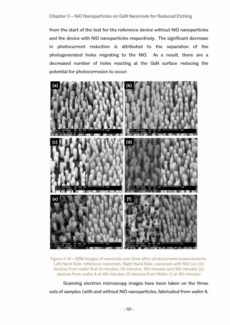
Chapter 5 – NiO Nanoparticles on GaN Nanorods for Reduced Etching
- 121 -
from the start of the test for the reference device without NiO nanoparticles
and the device with NiO nanoparticles respectively. The significant decrease
in photocurrent reduction is attributed to the separation of the
photogenerated holes migrating to the NiO. As a result, there are a
decreased number of holes reacting at the GaN surface reducing the
potential for photocorrosion to occur.
Figure 5-10 – SEM images of nanorods over time after photocurrent measurements. Left Hand Side: reference nanorods, Right Hand Side: nanorods with NiO (a)-(d) devices from wafer B at 15 minutes, 50 minutes, 105 minutes and 180 minutes (e)
devices from wafer A at 180 minutes (f) devices from Wafer C at 180 minutes
Scanning electron microscopy images have been taken on the three
sets of samples (with and without NiO nanoparticles, fabricated from wafer A,

Chapter 5 – NiO Nanoparticles on GaN Nanorods for Reduced Etching
- 122 -
B, and C, respectively) throughout the three hour test period to study the
corrosion issue, illustrated in Figure 5-10. As demonstrated, all three devices
with the NiO nanoparticles show an improved resistance to corrosion
compared to their individual references. Severe corrosion has been
observed by the NaOH solution on all the devices fabricated without NiO
cocatalyst, independent of indium content. It is very interesting to highlight
the stability of the upper p-type GaN on the nanorods. As previously
discussed the migration of electrons in p-type GaN to the surface prevents
oxidation due to the requirement of holes,17 leading to a reduction or
elimination of corrosion on p-GaN.18
Below the p-type layers are InGaN/GaN MQWs and n-GaN. Figure 5-
10(b) shows a clear etching of the parts below the p-type layers after 50
minutes testing, in particular, the InGaN/GaN MQWs, which is just below the
p-type layers. This is potentially due to increased reactions occurring in the
indium rich reasons, agreeing with the previous results based on PL
measurements on bulk InGaN films.19 After the total test time of 180 minutes,
the reference devices without NiO show severe corrosion, leading to
significantly thinned nanorods. The mechanism of the photochemical etching
of GaN in NaOH under UV illumination has been discussed in Chapter 2, which
can be described by the equations below in more detail,
2𝐺𝑎𝑁 + 6ℎ+ → 2𝐺𝑎3+ + 𝑁2 ↑ (1)
2𝐺𝑎3+ + 6𝑂𝐻− → 2𝐺𝑎2𝑂3 + 6𝐻+ (2)
𝐺𝑎2𝑂3 + 6𝑂𝐻− → 2𝐺𝑎𝑂3
3− + 3𝐻2𝑂 (3)
Incident photons, with energy above the band gap of GaN generate
electrons and holes. The migration of the holes to the surface of the GaN can
result in the formation of Ga ions (Equation 1). The resulting ions can then
react with the hydroxide ions in the solution forming an oxide layer on the
surface of nitride and the generation of hydrogen ions in solution (Equation
2). The formed oxide is then soluble in the presence of hydroxide ions
resulting in dissolution (Equation 3). This is the mechanism for the
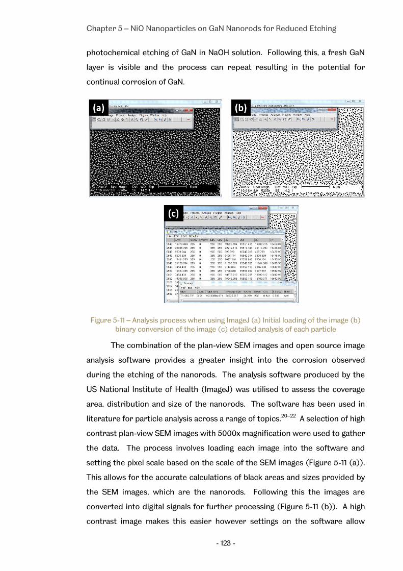
Chapter 5 – NiO Nanoparticles on GaN Nanorods for Reduced Etching
- 123 -
photochemical etching of GaN in NaOH solution. Following this, a fresh GaN
layer is visible and the process can repeat resulting in the potential for
continual corrosion of GaN.
Figure 5-11 – Analysis process when using ImageJ (a) Initial loading of the image (b) binary conversion of the image (c) detailed analysis of each particle
The combination of the plan-view SEM images and open source image
analysis software provides a greater insight into the corrosion observed
during the etching of the nanorods. The analysis software produced by the
US National Institute of Health (ImageJ) was utilised to assess the coverage
area, distribution and size of the nanorods. The software has been used in
literature for particle analysis across a range of topics.20–22 A selection of high
contrast plan-view SEM images with 5000x magnification were used to gather
the data. The process involves loading each image into the software and
setting the pixel scale based on the scale of the SEM images (Figure 5-11 (a)).
This allows for the accurate calculations of black areas and sizes provided by
the SEM images, which are the nanorods. Following this the images are
converted into digital signals for further processing (Figure 5-11 (b)). A high
contrast image makes this easier however settings on the software allow

Chapter 5 – NiO Nanoparticles on GaN Nanorods for Reduced Etching
- 124 -
control over the contrast in order to accurately calculate the sizes. Half
particles are removed prior to processing to increase the accuracy of the
results for which analysis of each particle is presented in a tabulated format
as illustrated in Figure 5-11 (c).
Comparison of the overall nanorod coverages from the SEM images
obtained with different testing time provides accurate information of the
corrosion as a result of photochemical etching. Figure 5-12 illustrates the
overall nanorod coverages as a function of testing time for the three sets of
devices. A clear downward trend in nanorod coverage is observable for the
samples without NiO, reducing by a value of 15 %, 15.7 % and 15.6 % for the
devices fabricated from wafers A, B and C respectively. In a remarkable
contrast, the counterparts coated with NiO cocatalyst demonstrate a
decrease of 0 %, 4.9 % and 3.1 % in nanorod coverage. Based on the SEM
images, the tops of the nanorods remain relatively intact throughout the
etching suggesting that the 15 % decrease in coverage observed for the
devices without NiO is a conservative estimate for the degradation suggesting
an even greater performance of the devices with NiO cocatalysts.
0 50 100 150 2000
10
20
30
40
50
Na
no
rod
Co
vera
ge
(%
)
Time (minutes)
A A w/NiO
B B w/NiO
C C w/NiO
Figure 5-12 – Nanorod coverage of all six devices with and without NiO based on ImageJ analysis of top-down SEMS, representative errors are illustrated for devices
from wafer B
Further to the analysis of the nanorod coverage, an investigation into
the change in nanorod radius has also been carried out. The radius was
calculated assuming circular nanorods by the equation πr2. Thousands of

Chapter 5 – NiO Nanoparticles on GaN Nanorods for Reduced Etching
- 125 -
data points were analysed for each step providing good reliability in regards
to results. Based on the analysis of each image a histogram of the data was
collected to group the data into proper categories, based on distribution in
terms of nanorod sizes. These were, <20 nm, 20>x<50 nm, 50>x<70 nm,
70>x<90 nm, 90>x<110 nm, 110>x<130 nm, 130>x<150 nm, 150>x<170 nm,
170>x<200 nm and 200>x<250 nm. Figure 5-13 illustrates the difference
between the devices with and without coated NiO nanoparticles, fabricated
from wafer B as an example. The initial maximum abundance peak is
exhibited at 130/150 nm for both wafers indicating a reasonable level of
uniformity in the samples prior to photoelectrochemical reactions. Figure 5-
13 indicates that the distribution of the nanorod radii remains largely
unchanged for the sample with NiO nanoparticles, while a clear shift to a
smaller size in terms of maximum radius has been demonstrated for the
reference device without NiO. In detail, the maximum radius decreases from
140 nm to 110 nm after the 3 hour photoelectrochemical tests.
100 150 200
0.0
0.5
1.0
Rela
tive A
bu
nd
an
ce
Fresh
15 Min
50 Min
110 Min
180 MinRela
tive A
bu
nd
an
ce
Nanorod Radius (nm)
Decreasing
100 150 200
0.0
0.5
1.0
(a) Wafer B
Fresh
15 Min
50 Min
110 Min
180 Min
(b) B w/NiO
Figure 5-13 – Distribution of nanorod sizes for (a) Wafer B and (b) Wafer B w/NiO
The addition of NiO has effectively protected the nanorods from
etching. The coverage of the nanorods for the samples with NiO remains
largely unchanged compared to the reference device without NiO in which a
40 % reduction from the initial coverage is observed, as shown in Figure 5-12.
Furthermore for the device with NiO nanoparticles, the radii remains similar
Chapter 5 – NiO Nanoparticles on GaN Nanorods for Reduced Etching
- 126 -
during the three hour test It is worth highlighting that the InGaN/GaN is
significantly protected from anodic corrosion as a result of the movement of
the oxidation reaction to the NiO nanoparticles
5.3 Conclusions
In summary, a considerable reduction in photoelectrochemical etching
and a significant enhancement in photocurrent have been achieved as a result
of the addition of the NiO nanoparticles to InGaN/GaN nanorod based
photoelectrodes for solar power water splitting in a NaOH electrolyte. The
increase in photocurrent is attributed to the band gap overlap of the NiO
nanoparticles with the device resulting in an increase in electron-hole
separation, aiding migration and then reducing recombination. Due to the
promotion of the oxidation reaction on the NiO surface as opposed to the
device surface, a reduction in the oxidative etching caused by the
photogenerated holes accumulated at the GaN/electrolyte interface has been
achieved. Thus the photoelectrochemical etching on the device is reduced.
Currently, the deposition technique results in the majority of NiO forming on
the tops of the nanorods. Altering the deposition method to either a
photodeposition technique or a calcination of solution deposited nickel could
lead to greater coverage on the nanorod sidewalls. As visible in the SEM
images, the sidewalls are etched faster than the tops of the nanorods,
therefore improving the coverage could potentially result in further
improvements in device lifetimes.

Chapter 5 – NiO Nanoparticles on GaN Nanorods for Reduced Etching
- 127 -
Bibliography
1 F.E. Osterloh, Chem. Soc. Rev. 42, 2294 (2013).
2 K. Maeda and K. Domen, J. Phys. Chem. Lett. 1, 2655 (2010).
3 A. Kudo and Y. Miseki, Chem. Soc. Rev. 38, 253 (2009).
4 K. Maeda, K. Teramura, D. Lu, N. Saito, Y. Inoue, and K. Domen, Angew. Chem. Int. Ed. Engl. 45, 7806 (2006).
5 X. Wang, G. Liu, L. Wang, Z.-G. Chen, G.Q.M. Lu, and H.-M. Cheng, Adv. Energy Mater. 2, 42 (2012).
6 T. Hisatomi, J. Kubota, and K. Domen, Chem. Soc. Rev. (2014).
7 K. Maeda and K. Domen, J. Phys. Chem. C 111, 7851 (2007).
8 H. Kato, K. Asakura, and A. Kudo, J. Am. Chem. Soc. 125, 3082 (2003).
9 R. Li, F. Zhang, D. Wang, J. Yang, M. Li, J. Zhu, X. Zhou, H. Han, and C. Li, Nat. Commun. 4, 1432 (2013).
10 K. Maeda, A. Xiong, T. Yoshinaga, T. Ikeda, N. Sakamoto, T. Hisatomi, M. Takashima, D. Lu, M. Kanehara, T. Setoyama, T. Teranishi, and K. Domen, Angew. Chemie 122, 4190 (2010).
11 X. Zong, H. Yan, G. Wu, G. Ma, F. Wen, L. Wang, and C. Li, J. Am. Chem. Soc. 130, 7176 (2008).
12 D. Wang, A. Pierre, M.G. Kibria, K. Cui, X. Han, K.H. Bevan, H. Guo, S. Paradis, A.-R. Hakima, and Z. Mi, Nano Lett. 11, 2353 (2011).
13 K. Ohkawa, W. Ohara, D. Uchida, and M. Deura, Jpn. J. Appl. Phys. 52, 08JH04 (2013).
14 S.H. Kim, M. Ebaid, J.-H. Kang, and S.-W. Ryu, Appl. Surf. Sci. 305, 638 (2014).
15 M. Ono, K. Fujii, T. Ito, Y. Iwaki, A. Hirako, T. Yao, and K. Ohkawa, J. Chem. Phys. 126, 054708 (2007).
16 M. Grätzel, Nature 414, 338 (2001).
17 K. Fujii and K. Ohkawa, Jpn. J. Appl. Phys. 44, L909 LP (2005).
18 K. Aryal, B.N. Pantha, J. Li, J.Y. Lin, and H.X. Jiang, Appl. Phys. Lett. 96, 052110 (2010).

Chapter 5 – NiO Nanoparticles on GaN Nanorods for Reduced Etching
- 128 -
19 M. Li, W. Luo, B. Liu, X. Zhao, Z. Li, D. Chen, T. Yu, Z. Xie, R. Zhang, and Z. Zou, Appl. Phys. Lett. 99, 112108 (2011).
20 Z. Cai, K.A. Vallis, and R.M. Reilly, Int. J. Radiat. Biol. 85, 262 (2009).
21 T. Collins, Biotechniques 43, S25 (2007).
22 C. a Schneider, W.S. Rasband, and K.W. Eliceiri, Nat. Methods 9, 671 (2012).

Chapter 6 – Nanoporous GaN for Enhanced Photoelectrochemical Activity
- 129 -
Chapter 6
Nanoporous GaN for Enhanced
Photoelectrochemical Activity
orous semiconductor materials have been widely investigated for
a variety of applications.1 The history of porous semiconductors is
a long one with their properties investigated as early as 1952.2 The
opportunity they offer is still far from being realised however the potential of
porous materials is vast.1,3 By means of a simple photoelectrochemical etching
approach in a KOH solution GaN nanoporous structures with controllable
pore sizes have been successfully fabricated. An enhancement in both
photocurrent and hydrogen generation has been achieved across all samples
with the nanoporous structure compared to their reference un-etched
counterparts. A significant enhancement in incident photon conversion
efficiency (IPCE) at the GaN band edge, 355 nm, has been achieved.
6.1 Porous Semiconductors in Water Splitting
A variety of porous semiconductors have been studied in water
splitting,4–7 including TiO2,8 WO39 and Fe2O3.10 The method of fabrication has
been shown to have a significant effect on photocurrent with a factor of 10x
change in efficiency for two porous TiO2 samples fabricated by different
techniques.8 The use of porous materials have been widely explored11–13 due
to their nano structure. As discussed in Chapter 4, the use of nanostructures
P

Chapter 6 – Nanoporous GaN for Enhanced Photoelectrochemical Activity
- 130 -
can lead to increases in device efficiency as a result of a variety of
mechanisms. A porous structure is expected to lead to an increase in surface
area of the semiconductor, increased light absorption and the potential for
reduced electron-hole recombination. Additionally the porous structures are
also expected to enhance the adsorption and desorption of reactants and
products.12 As a result, the turnover of reactions on the surface of a porous
device can be significantly higher than those observed in planar structures.
It is worth highlighting another advantage of a nanoporous structure
compared to the nanorod structures discussed in Chapter 4. With a porous
film, the pore size of the system can be engineering to a size complimentary
to that of the minority carrier diffusion length of the semiconductor.9 In
addition, porous structures have been shown to be more effective at
absorption of longer wavelengths by controlling the pore size of the
structure.10 It is therefore important to exhibit control over the fabrication
technique to produce porous devices with suitable pore sizes and networks.
For oxide semiconductors common methods include sol-gel synthesis in
which a mixture of precursors is prepared before deposition and heat
treatments results in the formation of the porous structure. Alternatively,
chemical etching or templating techniques have been utilised.3 The
fabrication technique varies across different material groups with etching
and anodization methods utilised in III-V semiconductors.14,15
6.2 History of Porous GaN & InGaN
In principle, GaN exhibits remarkable resistance to standard wet
chemical solutions,16 similar to that of diamond and sapphire. Recently,
photoelectrochemical (PEC) etching under ultraviolet (UV) illumination,
where the photon energy is above the GaN band gap, could be implemented
on GaN.17–19 In 1996, it was found that porous GaN could be fabricated via an
photochemical etching technique.20 The initial method proceeded via the
anodization of a hydride vapour phase epitaxial grown GaN wafer in
hydrofluoric acid under UV illumination. The pores were found to permeate
through the wafer close to the [0001] direction and formed by corrosion of

Chapter 6 – Nanoporous GaN for Enhanced Photoelectrochemical Activity
- 131 -
the n-type material. It was suggested that the etching occurs at irregularities
in the surface of the material such as defects leading to the reaction of the
electrolyte at these areas, resulting in the formation of the pores.21 Further
investigation revealed a reduction in residual stress of the porous layer due
to the pore formation at the boundaries of the GaN crystallites. Figure 6-1
illustrates an AFM image of the early porous structures, with pores in the
region of 150 nm.
Figure 6-1 - AFM image of early porous GaN layer, inset image displays an enlarged single pit, greyscale of image corresponds to height variation of 150 nm. Adapted from (Mynbaeva, 2000)21 and permission obtained from copyright holder © AIP
Publishing
Alternate methods in the fabrication of porous GaN have been via
electrochemical and photoelectrochemical etching and metal assisted
electroless etching. The solutions used in each case are varied, but are
typically acids or bases.22 In each case control over the pore size and
properties can be controlled by altering the fabrication conditions. Li et al.
utilised a metal assisted approach in an ethanol, HF and hydrogen peroxide
solution and a UV illumination source.23 Control over the structure was
exhibited with respect to etching time and position of the deposited metal. In
electrochemical and photoelectrochemical etching, all variables have an
effect on the fabrication of the porous structure.24–27 Youtsey has
investigated the effects of PEC etching with potassium hydroxide in which a
great degree of control has been exhibited.17,28–31 The variation in illumination
intensity and electrolyte concentration can result in diffusion or carrier
limitations. High illumination intensity creates a surplus of carriers leading to

Chapter 6 – Nanoporous GaN for Enhanced Photoelectrochemical Activity
- 132 -
the diffusion of carriers to the electrolyte limiting the reaction. Alternatively,
if illumination intensity is low the number of carriers limits the overall rate of
reaction. Porous InGaN has been formed by etching in HF and more recently
via UV assisted electrochemical (PEC) etching.32 Relatively small pores were
formed in the InGaN with the KOH solution due to the short etching time.
Currently, there are no published reports on porous GaN nanorod structures
however porous nanowires have been grown by thermal chemical vapour
deposition with pore sizes in the range of 5-20 nm on 10-80 nm nanowires.33
Nanoporous GaN has wide applications. Porous structures have been
utilised as growth templates,26,34,35 upper layers on LED devices36–38 and in gas
sensing applications.39–41 In the case of porous GaN for use as growth
templates, lateral overgrowth techniques on the porous templates has
resulted in strain relaxation of the bulk material leading to improved chemical
and optical properties.21,42–44 For LED devices, roughening of the structure
and partial strain relaxation have been identified as reasons behind the
improved device performances.37
6.2.1 Etching Process
Photoelectrochemical etching of GaN is essentially the same process
as anodic etching which was described in Chapter 2 and 5. PEC etching in a
basic medium proceeds via the following reactions.
2𝐺𝑎𝑁 + 6ℎ+ → 2𝐺𝑎3+ + 𝑁2 ↑ (i)
2GaN + 6OH− + 6h+ → 2Ga2O3 + 3H2O + N2 ↑ (ii)
Ga2O3 + 6OH− → 2GaO3
3− + H2O (ii)
Equation 6-1 – Photoelectrochemical etching mechanism of GaN
It is therefore possible to control the reaction through the hydroxide
ion concentration and the number of photogenerated holes under
illumination. Variation in either of these can therefore alter the nature of the
reaction. There is also a dependence on crystal orientation in regards to GaN,
with the N and Ga terminated faces behaving differently in different

Chapter 6 – Nanoporous GaN for Enhanced Photoelectrochemical Activity
- 133 -
conditions.22 The etching proceeds via the formation of an oxide layer on the
GaN surface which is dissolvable in a hydroxide solution. As a result, the
formed oxide is continually formed and then dissolved throughout the
duration of the reaction. Without the presence of photogenerated holes at
the surface the reaction cannot proceed. Therefore without a source of
illumination or if p-GaN is utilised no etching will be observed.17 As alluded to
previously, the etching proceeds via recombination centres. Defects within
the GaN surface can serve as traps for electrons and holes leading to the
recombination of the carriers preventing etching. As a result, typically the
centre of the GaN crystal structures are attacked as opposed to the
threading dislocations in the epitaxial layer.26,45 After the initial layers are
etched, successive growth layers beneath the surface layer can be attacked
resulting in the formation in a network of pores in the structure.
6.2.2 Etched GaN/InGaN in Water Splitting
PEC etching has been utilised for the formation of highly smooth
surfaces,30 defect idetification46 and enhanced LED light output.47 However,
despite the long history in the fabrication of porous GaN it has been hardly
implemented in its application in water splitting. Guo et al. prepared porous
GaN via a platinum assisted electroless etch which resulted in an enhanced
UV photocurrent response.48 The increased response was attributed to the
change in conductive area. This report demonstrated the potential for an
increase in photocurrent of porous GaN however did not investigate the
potential in water splitting. Ryu et al. reported both electrochemical etching
and photoelectrochemical etching of GaN for water splitting.49 In their report,
the nanoporous GaN was fabricated in a 0.3 M oxalic acid solution with a
supplied voltage of 15 V for 10 minutes. The pores were approximately 30 nm
in diameter with a density of 2.9 x1010 cm-2. The response of the
electrochemically etched device was higher than the planar sample which
was attributed to an increase in surface area and enhanced hole transport.
Interesting to note in their report is due to the enhanced formation of
defects as a result of their photoelectrochemical etching, a detrimental effect
on photocurrent is observed.50

Chapter 6 – Nanoporous GaN for Enhanced Photoelectrochemical Activity
- 134 -
There are other etching techniques reported, where improvements in
photocurrent have been achieved. In these cases, the etching has been
utilised as a surface treatment to remove defects as opposed to the
fabrication of nanoporous GaN.51,52 Basilio et al. utilised a PEC etch in KOH
and a hot H3PO4 treatment. After the initial PEC process the photocurrent of
the system had reduced significantly with a delayed turn-on compared to the
pristine sample.51 This was attributed to an increase in localised carrier
concentrations at the surface of the semiconductor and the formation of non
c-plane facets causing the delayed turn-on. Li et al. have reported the only
use of an etch treatment on an InGaN based device.52 An electrochemical
treatment was conducted in 1 M HCl leading to an enhanced photocurrent
and incident photon conversion efficiency. Due to the growth of bulk InGaN,
indium rich regions were present at the surface leading to recombination
centres. It was posed that the etch process removes these allowing for
better separation of the electron and holes resulting in an increase in the
photocurrent of the device.52
6.3 Nanoporous GaN
The benefits observed in oxide semiconductors due to the fabrication
of porous structures have not yet been fully explored in III-nitride based
devices. Current reports indicate the potential for electrochemical etching
of GaN however this has not gone further than simple porous structures.
Alongside this, porous InGaN devices have not yet been investigated for water
splitting.
6.3.1 Fabrication
Planar Porous GaN
A typical as-grown wafer is prepared via MOCVD growth technique as
previously described in Chapter 4. Following this a photoelectrochemical
etch is utilized as the process to form the nanoporous devices. The
photoelectrochemical etch follows a similar procedure to typical
photoelectrochemical device assessment. GaN samples with an insulated
Ti/Au ohmic contact acts as the working electrode in a photoelectrochemical
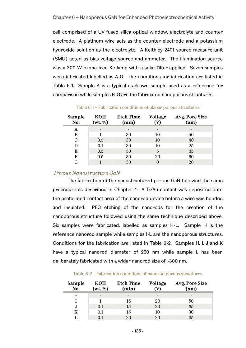
Chapter 6 – Nanoporous GaN for Enhanced Photoelectrochemical Activity
- 135 -
cell comprised of a UV fused silica optical window, electrolyte and counter
electrode. A platinum wire acts as the counter electrode and a potassium
hydroxide solution as the electrolyte. A Keithley 2401 source measure unit
(SMU) acted as bias voltage source and ammeter. The illumination source
was a 300 W ozone free Xe lamp with a solar filter applied. Seven samples
were fabricated labelled as A-G. The conditions for fabrication are listed in
Table 6-1. Sample A is a typical as-grown sample used as a reference for
comparison while samples B-G are the fabricated nanoporous structures.
Table 6-1 – Fabrication conditions of planar porous structures
Sample No.
KOH (wt. %)
Etch Time (min)
Voltage (V)
Avg. Pore Size (nm)
A - - - - B 1 30 10 50 C 0.5 30 10 40 D 0.1 30 10 25 E 0.5 30 5 35 F 0.5 30 20 60 G 1 30 0 20
Porous Nanostructure GaN
The fabrication of the nanostructured porous GaN followed the same
procedure as described in Chapter 4. A Ti/Au contact was deposited onto
the preformed contact area of the nanorod device before a wire was bonded
and insulated. PEC etching of the nanorods for the creation of the
nanoporous structure followed using the same technique described above.
Six samples were fabricated, labelled as samples H-L. Sample H is the
reference nanorod sample while samples I-L are the nanoporous structures.
Conditions for the fabrication are listed in Table 6-2. Samples H, I, J and K
have a typical nanorod diameter of 220 nm while sample L has been
deliberately fabricated with a wider nanorod size of ~300 nm.
Table 6-2 – Fabrication conditions of nanorod porous structures
Sample No.
KOH (wt. %)
Etch Time (min)
Voltage (V)
Avg. Pore Size (nm)
H - - - - I 1 15 20 50 J 0.1 15 20 35 K 0.1 15 10 30 L 0.1 20 20 35
Chapter 6 – Nanoporous GaN for Enhanced Photoelectrochemical Activity
- 136 -
6.3.2 Characterisation
As discussed the fabrication conditions are vitally important in the
fabrication of a nanoporous structure in GaN. It is however very easy to alter
the concentration and voltage supplied during PEC etching to obtain the
necessary control. A set of as-grown and nanorod samples were fabricated
from a set of GaN wafers that were grown in the same growth run. Hall
measurements were conducted on the sample indicating a doping level of 1.3
x1018 cm-3. The doping level plays a role within the etching of the material due
to its conductivty.28 The n-type layer has a thickness of 1.8 µm. For the
fabrication of nanoporous structure, the influence of the applied voltage and
etchant concentrations have been systematically studied. Two sets of
nanoporous structures have been fabricated, (1) nanostructures fabricated
from the planar as-grown wafer; (2) nanostructure fabricated from the
prepared nanorod arrays (the detailed fabrication of nanorod array
structures can be found in Chapter 4). Table 6-1 and Table 6-2 provide
fabrication summaries of the nanostructures fabricated from the planar as-
grown structures and nanorod structures respectively. A concentration
gradient of 0.1-1 wt % was utilised as well as voltages ranging from 0 to 20 V
for the planar structures. Etch times were set at a maximum of 30 minutes
and the measured illumination intensity ~200 mA cm-2. The conditions were
similar for the nanorods however the etch time was reduced to take into
account the considerably larger active surface area of the fabricated
nanorods.
Photoluminescence
Photoluminescence (PL) was performed using a 325 nm He-Cd laser
dispersed by a 0.75 m monochromator and detected by an ultraviolet
enhanced CCD detector for all samples. The normalised spectrum for the
planar porous samples is presented in Figure 6-2. For all the samples, a red
shift in emission wavelength has been observed. In detail, a red shift of 1.2 nm
for samples B, C and D has been observed, and 1.7 nm for sample E, 1.9 nm for
sample F and 1 nm for sample G, respectively. In agreement with Yam53 there
is no clear correlation between shift in emission wavelength and pore size.

Chapter 6 – Nanoporous GaN for Enhanced Photoelectrochemical Activity
- 137 -
However, interesting to note is a potential relationship between peak shift
and etch voltage. Looking at samples G, E and F with etch voltages of 0, 5 and
20 V respectively, the peak shift increases from 1 to 1.9 nm. This is likely
related to the degree of etching that has occurred relating to the level of
relaxation in the bulk GaN.
350 355 360 365 370 375 380 3850.0
0.5
1.0N
orm
ali
se
d I
nte
ns
ity
(a
u)
Wavelength (nm)
Sample A (ref.)
Sample B
Sample C
Sample D
Sample E
Sample F
Sample G
Figure 6-2 – Normalised room temperature PL spectra of nano porous structures fabricated from a planar as-grown wafer
Due to a large lattice-mismatch of ~16% between GaN and sapphire
substrate, GaN epitaxial layers on sapphire suffer from a great compressive
strain. Under fully strained conditions the compressive strain present within
a GaN substrate grown on an AlN buffer layer on sapphire is approximately
0.2 GPa for the GaN and 1.77 GPa for the AlN.54 As a result of the formation of
the nanoporous structures the strain can be largely relaxed, leading to the
red shift observed in PL emission peak. The extent of red-shift depends on
the degree of relaxation. From the data, the level of strain relief can be
estimated using the proportionality factor (K), where K=21.2±3.2 meV/GPa for
GaN.54 From the least to most severe peak shift, total strain relief is from 0.43
meV to 0.85 meV which indicates a significant reduction in total compressive
strain. The data shown in Figure 6-2 is comparable to the previous reports on
porous GaN where the relaxation has been confirmed by Raman
spectroscopy.24,44

Chapter 6 – Nanoporous GaN for Enhanced Photoelectrochemical Activity
- 138 -
350 360 370 380
PL
In
ten
sit
y (
a.u
.)
Wavelength (nm)
Sample A (ref.)
Sample H
I
J
K
L
Figure 6-3 – Room temperature PL for nanoporous nanorod samples H-M. The as-grown sample A has been included as a reference.
Room temperature PL of the nanoporous structures fabricated from
the prepared nanorod samples was also conducted. As previously discussed,
the formation of a nanorod array causes a reduction in strain compared to
the as-grown sample. This leads to a red shift as observed in Figure 6-3. For
the fabricated nanorods the shift observed is 2.4 nm or a strain relief of ~1
GPa, which indicates an almost complete release in compressive strain. The
peak shifts of the porous samples vary from 1-2.4 nm with samples etched
under a lower concentration (K and L) exhibiting the largest peak shift
compared to the as-grown sample. The difference in peak shift of the porous
samples is attributed to the changing etching conditions resulting in varied
porous structures.
Full width half maximum measurements of the room temperature PL
reveal values of 5.75 nm for the as-grown reference sample (A) and 8, 6.1, 6.2,
6.3 and 8.3 nm for samples H-L respectively. This suggests that the relative
contribution of the nanorods and porous structure towards the strain relief
changes dependent on the level of etching. The change in intensity observed
for each sample also varies depending on the etch conditions. The
enhancement in PL emission for the porous nanorod samples can be
attributed to an enhancement in extraction and also in absorption due to
scattering between and within the nanopores of the nanorods and an

Chapter 6 – Nanoporous GaN for Enhanced Photoelectrochemical Activity
- 139 -
increase in surface area resulting in an increase in greater number of excited
carriers.24,25,55
SEM Measurements
The morphology of the nanoporous samples was investigated by
scanning electron microscopy. Figure 6-4 illustrates a typical cross sectional
image and plan view images of each etched sample. In Figure 6-4(a) two
layers are clearly visible. One is a nominally doped GaN layer and an AlN
buffer with a total thickness of 0.8 m for the lower part (see sample
preparation section), and another is an n-doped GaN with a thickness of 1 m
for the upper part. It is clear that the nanopores are formed in the n-doped
GaN layer only, confirmed by observing a visible termination of the pores at
the boundary between the doped and undoped layer. Compared to the initial
n-GaN layer thickness a decrease of over 500 nm is observed. The pores also
follow a linear structure through the wafer indicating that the etching occurs
at the grain centres as previously discussed. The termination of the etching is
attributed to the significant difference in carrier concentration between the
intrinsic and doped GaN. As a result, the resistivity of the intrinsic GaN is
considerably higher than n-doped GaN preventing effective carrier flow,
thereby preventing the etching of the lower wafers. This indicates that a level
of control by varying dopant concentration could be achieved.28
The sizes of nanopores has been examined through measuring the top-
down SEM images, which are given in Figure 6-4b, c, d, e, f and g,
corresponding to sample B, C, D, E, F and G respectively. Sample B, C and D
form one group, where the samples were fabricated as a function of KOH
concentration under an identical voltage. Another group of samples,
consisting of sample E, C and F, were fabricated as a function of a supplied
voltage from 5 to 20 V but using the same KOH concentration. Sample G is
comparable to sample B due to identical etchant concentrations however the
applied voltage has been reduced to 0 V to assess the etchant rate due solely
to illumination. As a result of hydroxide ion consumption in both the
formation and dissolution reactions (refer to Equations 2 and 3), the
concentration of the KOH etchant is essential in controlling whether the

Chapter 6 – Nanoporous GaN for Enhanced Photoelectrochemical Activity
- 140 -
reaction is carried out under a mechanism due to diffusion (low
concentration, high illumination) or carrier (high concentration, low
illumination) limitations.
Figure 6-4 – SEM images of porous GaN samples. (a) typical cross section of porous samples obtained from sample C. (b)-(g) top down SEM images of samples B-G
respectively

Chapter 6 – Nanoporous GaN for Enhanced Photoelectrochemical Activity
- 141 -
With an increase in KOH solution an increase in pore size has been
obtained (Samples B, C and D) as altering the KOH concentration ultimately
changes the concentration of the total ions in the reaction, increasing the
availability of hydroxyl ions and therefore generating a greater number of
etch sites across the GaN surface as the hydroxyl ions permeate through the
solution. At low ion concentrations (0.1 wt %, Sample D), there is a limit to the
number of interactions at the semiconductor-KOH interface and therefore
under diffusion controlled scenarios a reduced degree of etching is observed.
Altering the bias conditions of the etching also leads to a change in the
number of ions in solution, as above the reduction-oxidation potential of
water (1.23eV) there is an increase in the dissociation of the electrolyte and
therefore an increase in the OH- concentration. Alongside this, when under
bias, the separation of the photogenerated electron-hole pairs is more
efficient as a result of the increased conductivity, further increasing the
number of potential reactions. Therefore, as observed an increase in the
degree of etching occurs at higher biases (Sample F). In agreement with this,
the etching of sample G occurs purely from the photogenerated carriers
which results in a lesser etch.
Similar observations have been observed in the fabrication of
nanoporous structures prepared from the nanorod structures with the more
enhanced etch conditions (such as higher concentration of KOH) resulting in
a greater degree of etching, which can be observed in Figure 6-5. Comparing
samples I, J and K in Figure 6-5(b), (c) and (d) Sample I exhibits a significant
degradation as a result of the higher concentration of the KOH etchant used
compared to that for samples J and K, leading to a significant reduction in the
nanorod structure while samples J and K retain the nanorod structure.
FWHM measurements of the room temperature PL provide supporting
evidence towards these results. For the reference as-grown and nanorod
structures a value of 5.7 nm and 8 nm is obtained. As the etch severity
decreases the FWHM of samples I, J and K, increases to values more similar to
that of the un-etched nanorod from values of 6.1, 6.2 and 6.3 nm respectively.
Furthermore, the nanoporous nanorod sample with a wider diameter
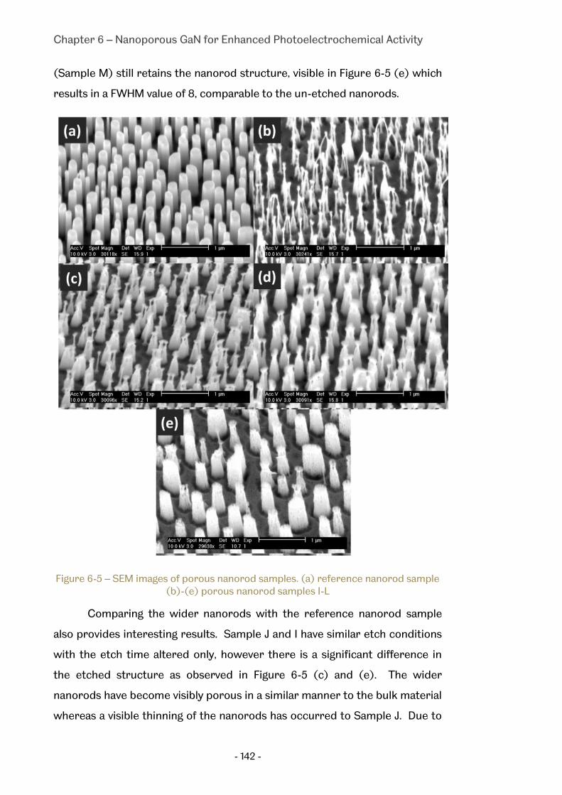
Chapter 6 – Nanoporous GaN for Enhanced Photoelectrochemical Activity
- 142 -
(Sample M) still retains the nanorod structure, visible in Figure 6-5 (e) which
results in a FWHM value of 8, comparable to the un-etched nanorods.
Figure 6-5 – SEM images of porous nanorod samples. (a) reference nanorod sample (b)-(e) porous nanorod samples I-L
Comparing the wider nanorods with the reference nanorod sample
also provides interesting results. Sample J and I have similar etch conditions
with the etch time altered only, however there is a significant difference in
the etched structure as observed in Figure 6-5 (c) and (e). The wider
nanorods have become visibly porous in a similar manner to the bulk material
whereas a visible thinning of the nanorods has occurred to Sample J. Due to

Chapter 6 – Nanoporous GaN for Enhanced Photoelectrochemical Activity
- 143 -
the differences in surface area, the recombination dynamics of the two
samples will be different resulting in the appearance change. This also
indicates that a wider structure is required to create similar pores to those
observed in the bulk material which may offer performance benefits over the
reference sample.
6.3.3 Solar Hydrogen Performance
Hydrogen generation potential has been assessed by measuring the
photocurrent of the devices. These tests were conducted in HCl, a standard
electrolyte for water splitting, where GaN exhibits high chemical resistance.
The measurements have been conducted in a 1 M solution under solar filtered
Xe lamp illumination at 100 mW cm-2. Figure 6-6 (a) shows the typical
photocurrent as a function of bias for the different GaN nanoporous
structures under both illumination and dark conditions, where the set of GaN
nanoporous structures (fabricated from a planar as-grown GaN layer) were
fabricated based on the utilisation of KOH with different concentrations, i.e.,
sample B, C and D, respectively. As a reference, the data for the as-grown
GaN structure (labelled as sample A) is included. As demonstrated in the
SEM shown in Figure 6-4, an increase in the concentration of the fabrication
solution (i.e., KOH) results in larger pores, and as observed from the
photocurrent measurements (Figure 6-6 (a)) an enhancement in
performance. In fact, nearly all the photoelectrodes fabricated based on the
nanoporous structure exhibit an increase in photocurrent compared to the
as-grown device. This is thought to be attributed to the increase in surface
area gained from the creation of a nanoporous structure. This provides a
greater number of active areas for the solution to react with the surface, thus
allowing greater current flow between the semiconductor and electrolyte.
Not only this, the nanoporous structure will also create cavities in which the
incident light can propagate through the sample, leading to significant
enhancement in the total amount of radiation absorbed. Without a significant
level of etching, as observed in Sample G, an increase in photocurrent is not
observed.

Chapter 6 – Nanoporous GaN for Enhanced Photoelectrochemical Activity
- 144 -
-1 0 1 2
0.0
0.1
0.2
0.3
0.4
Dark
A
B
C
D
G
Cu
rren
t D
en
sit
y (
mA
cm
-2)
Voltage (V vs VCE
)
(a)
Dark
-1 0 1 2
0.0
0.1
0.2
0.3
0.4
(b)
Cu
rren
t D
en
sit
y (
mA
cm
-2)
A
E
C
F
Figure 6-6 – Photocurrent as a function of bias under dark and illuminated conditions for (a) the samples fabricated under difference KOH concentrations; and
(b) the samples fabricated under different voltages supplied
Figure 6-6 (b) shows the typical photocurrent as a function of bias
under both illumination and dark conditions for the nanoporous structures
fabricated using the different supplied voltages but identical KOH
concentrations, i.e., sample E, C and F, respectively. As shown in Figure 6-4, an
increase in voltage supplied results in a rise in pore size. Consequently, it
leads to significant enhancement in photocurrent for assessing the solar
hydrogen performance, which is similar to Figure 6-6 In comparison to the
un-etched as-grown sample across the potential working voltages (0-1V) the
increase in photocurrent for samples B, C and D are 308 %, 253 % and 222 %
respectively, where the pore sizes of sample D, C and B are in an increasing
order. This suggests that the fabrication of nanoporous GaN used as a
photoelectrode is a very efficient and cost-effective approach to achieving
significant improvement in energy conversion efficiency. Comparison of the
two GaN sets of samples suggests that it is more efficient to fabricate the
nanoporous structures with larger pore size through increasing the supplied
voltage. For instance, Sample F, which was fabricated using 20 V, the highest
voltage used in the present study, demonstrates the highest enhancement in
photocurrent, which is 390 % higher over the aforementioned working
voltages than that for the as-grown sample (i.e., sample A). Comparing the

Chapter 6 – Nanoporous GaN for Enhanced Photoelectrochemical Activity
- 145 -
efficiency of the as-grown device and sample F, the performances increases
from 0.1 % to 0.43 % when no bias is applied, a factor of 4 improvement.
-1 0 1 2
0.0
0.1
0.2
0.3
0.4
Cu
rren
t D
en
sit
y (
mA
cm
-2)
Voltage (V vs VCE
)
Sample A
Sample H
Sample I
Sample J
Sample K
Sample L
Figure 6-7 – Photocurrent as a function of bias for the reference as grown device (Sample A), reference nanorod device(Sample H) and porous nanorod devices
(Samples I-L)
Similar results have also been observed in the nanoporous structures
fabricated from nanorod templates. As discussed in Chapter 4, the
fabrication of a nanorod structure can increase the performance of a device
significantly over an as-grown device. The reference nanorod device (Sample
H) fabricated in this sample set results in a two-fold increase compared to
the as-grown device (Sample A). Photocurrent measurements at biases from
-1 V to 2 V are illustrated in Figure 6-7. In contrast to the planar porous
structures, a reverse relationship between etch severity and photocurrent is
observed with Sample K demonstrating the greatest improvement in
photocurrent compared to the reference nanorod device. Compared to non-
porous reference nanorod device the averaged change in photocurrent over
0 – 1 V is 102 %, 142 %, 168 % and 110 % for samples I-L, respectively. Sample I
has a similar response to the reference nanorod device. Based on the severe
etching of the nanorods visible in Figure 6-5 a decrease in photocurrent
would’ve been expected due to the enhanced damage of the device. However,
the photocurrent remains unchanged which is attributed to the fabrication of
the porous bulk GaN layer beneath the fabricated nanorods which has been
shown to increase photocurrent. With a decrease in etch severity, the

Chapter 6 – Nanoporous GaN for Enhanced Photoelectrochemical Activity
- 146 -
combined benefits of a nanorod and porous structure can be obtained, as
demonstrated in samples J-L. Despite this, Sample L, with obvious pores
within the nanorods does not generate the greatest change in photocurrent.
Based on the room temperature PL FWHM measurement, Sample L indicates
a value closest to the reference nanorod structure (Sample H); this suggests
that the bulk layer is not as severely etched as samples I-K which indicates
that the total surface area may not have increased to the same extent as
Samples J and K.
Hydrogen Generation
Assessment of the hydrogen generation performance was conducted
for selected comparative samples and is detailed in Figure 6-8. The volume of
hydrogen was collected via the use of an upturned burette over the platinum
electrode allowing bubbles to displace a small volume of water. Theoretical
volumes of hydrogen were calculated from the obtained photocurrent values
using Equation 4,
𝑑𝑁𝐻2
𝑑𝑡=
𝑖
𝑛𝐹 (4)
where i is the number of current, n is the number of electrons
required, F is the Faraday constant and 2HN is the moles of hydrogen
produced. This can be converted into millilitres assuming a volume of 22.4
dm3 mol-1 for hydrogen gas under standard temperature and pressure. All
samples show a good agreement with the theoretical values, with slight
discrepancies attributed to the visual inspection of the burette. The
nanoporous GaN samples in Figure 6-8 all had a planar area prior to porous
fabrication within 0.02 cm-2 of each other based on detailed measurements
on the sample surface and are therefore comparable. In good agreement
with the previous photocurrent results, the ability of the porous samples for
hydrogen generation is increased with Sample D demonstrating a two fold
increase and Sample K a threefold increase over the reference as-grown
sample (Sample A). As discussed, this is attributed to the increase in surface

Chapter 6 – Nanoporous GaN for Enhanced Photoelectrochemical Activity
- 147 -
area of the samples allowing for improved charge-transfer and the better
adsorption and desorption properties of the nanoporous structure.
0 10 20 30 40 50 600.0
0.1
0.2
0.3
0.4
0.5
0.6
0.7
0.8
Measured
Sample A
Sample B
Sample H
Sample K
Hyd
rog
en
Vo
lum
e (
ml)
Time (minutes)
Theoretical
Figure 6-8 – Measured (points) and theoretical (solid lines) hydrogen values for porous samples at 0.8 V bias in HCl under 500 mW cm-2 illumination for as-grown
GaN (A), porous GaN (D), nanorod GaN (H) porous nanorod GaN (K)
Incident Photon Conversion Efficiency
The wavelength dependent performance, namely, incident photon
conversion efficiency (IPCE), an important performance indicator, can be
calculated using Equation 4 below,
𝐼𝑃𝐶𝐸(%) = 1240 ×𝐽(𝑚𝐴𝑐𝑚−2)
𝜆(𝑛𝑚)×𝐼(𝑚𝑊𝑐𝑚−2)× 100% (5)
where J is the photocurrent density, λ the wavelength of incident light
and I the incident power density. The IPCE of all samples except G and L have
been measured using a 75 W xenon lamp over a wavelength range of 320-600
nm, which are shown in Figure 6-9. All the GaN nanoporous samples, as
expected, demonstrate a significant increase in IPCE compared with the
reference as-grown sample (Sample A).
The response from the GaN samples extends from the deep UV until a
sharp decline after the band edge emission at 355 nm. This is as a result of
the band gap of GaN at 3.6 eV, therefore due to the low availability of solar
energy it is vital to increase the efficiency at the available wavelengths. The
porous planar samples shown in Figure 6-9(a) indicate a similar trend to

Chapter 6 – Nanoporous GaN for Enhanced Photoelectrochemical Activity
- 148 -
those observed from the photocurrents with Sample F performing better
than all other samples. Comparatively, the performance of the reference as-
grown sample at the GaN band edge of 355 nm is 20.7 % comparable with
other reports for GaN56,57 while the efficiency of Sample F is 43.4 % over
twice that of the reference as-grown structure indicating that the porous
structure has significantly enhanced the utilisation of the photo generated
carriers. Alongside this the efficiency of the reference nanorod structure is
49 % while the porous nanorod, Sample K, has a peak efficiency of 69.3 % at
355 nm. The decrease in distance for the minority carriers to diffuse, along
with the reduction in recombination centres due to the creation of the
porous structures causes the enhancement in IPCE observed in the
nanoporous planar and nanoporous nanorod samples.
320 360 560 6000
20
40
60
80
100(b)
Sample A
Sample B
Sample C
Sample D
Sample E
Sample F
IPC
E (
%)
Wavelength (nm)
(a)
350 560 6000
20
40
60
80
100
IPC
E (
%)
Sample H
Sample I
Sample J
Sample K
Figure 6-9 – Incident Photon Conversion Efficiency (IPCE) as a function of wavelength for (a) GaN based nanoporous structures and (b) the porous nanorod
structures
6.3.4 Summary
The fabrication of porous structures via photoelectrochemical etching
in a potassium hydroxide solution has resulted in an improvement in the
performance of planar and nanorod devices. Control over the severity of the
etch has been obtained through altering the concentration, voltage and etch
time. This has resulted in a specific control in pore size in which larger pores
have resulted in the greatest enhancement in the planar devices.

Chapter 6 – Nanoporous GaN for Enhanced Photoelectrochemical Activity
- 149 -
Comparatively, the nanorod structure requires milder etch conditions to
prevent the complete degradation of the nanorod structure and generate a
porous structure. Altering the diameter of the nanorod leads to a decrease in
total etch of the bulk GaN indicating further etching is required to achieve the
optimum increase with larger nanorods. Photocurrent measurements
increase by a factor of four for the planar porous device compared to the
reference as-grown device while the porous nanorods demonstrate a two
fold increase over the reference nanorod device.
The nanoporous structure increases the surface area of the device as
well as providing benefits for hydrogen generation due to improving the
adsorption and desorption properties of the GaN. Alongside this, the porous
structure decreases the distance required for the photo generated carriers
to migrate to the semiconductor-electrolyte interface. The work conducted
is also one of the only reports on porous nanostructured GaN and
demonstrates the potential of a KOH etch for enhanced photocurrents.
6.4 NiO Nanoparticles on Nanoporous GaN
Due to the potential issue of corrosion arising with the creation of a
nanostructure, as observed in Chapter 5, methods to quell this reaction are
required. As observed with the nanorod structures, the addition of NiO
resulted in a marked improvement in both photocurrent and corrosion
prevention.
6.4.1 Fabrication
A reference as grown n-GaN wafer with a doping density of 1.7 x 10¹⁸
cm-3 was utilised for the fabrication of a nanoporous device. A typical Ti/Au
ohmic contact was thermally deposited onto the sample prior to the bonding
of a copper wire with conductive epoxy. The contact was then insulated
before testing occurred. As with the samples previously fabricated, a PEC
etch method was implemented using a 1 wt % KOH etchant solution, 20 V bias
and an etch time of 30 minutes. The GaN acted as the working electrode
while a platinum rod acted as the counter electrode. Following porous
fabrication, the contact was lifted off from the device leaving an un-etched

Chapter 6 – Nanoporous GaN for Enhanced Photoelectrochemical Activity
- 150 -
contact area and a nanoporous area on the device. The NiO formation
followed the same method discussed in Chapter 5. Namely, the deposition of
an 8 nm nickel film, annealing at 820 °C in a nitrogen atmosphere to form
nickel nanoislands and finally an oxidation stage at 520 °C for 30 minutes
leading to the formation of NiO nanoparticles on the surface of the device. An
ohmic contact was then re-deposited and insulated for device
characterisation.
6.4.2 Characterisation
Figure 6-10 – SEM images of (a) nanoporous sample (b) nanoporous sample with NiO nanoparticles
SEM images of the device were taken before and after the NiO
deposition. As visible in Figure 6-10 the nanoporous sample has a network of
pores averaging 70 nm in diameter. The pores have formed within the grain
centres as observed in previous samples with an almost circular shape. After
the deposition and formation of the NiO, the NiO particles are observable
across the sample with a relatively uniform diameter of 200 nm.
6.4.3 Solar Hydrogen Performance
Photocurrent measurements for the two samples were taken under
one sun illumination in a 1 M HCl solution. Measurements were conducted as
a function of voltage and versus a prolonged time period to assess the effect
of the NiO on the porous GaN. As demonstrated in Figure 6-11, the addition of
the NiO causes a delayed turn-on voltage when compared to the porous
structure due to the difference in band alignments of the device due to the
NiO addition. Despite the delayed turn-on, at applied biases, as observed

Chapter 6 – Nanoporous GaN for Enhanced Photoelectrochemical Activity
- 151 -
previously, the NiO nanoparticles provide an enhancement in the
photocurrent of the device due to the enhanced separation of the electrons
and holes due to the discontinuity in the conduction and valence bands of the
GaN and NiO. Assessment of the stability of the device was conducted over a
three hour period (Figure 6-11(b)). The photocurrent of the device is
relatively stable indicating that no etching of the device is occurring.
-1 0 1 2
0.0
0.1
0.2
0.3
Cu
rren
t D
en
sit
y (
mA
cm
-2)
Voltage (V vs VCE
)
Porous
Porous w/ NiO
0 100 2000.0
0.2
0.4(b) Porous w/ NiO
Cu
rren
t D
en
sit
y (
mA
cm
-2)
Time (minutes)
(a)
Figure 6-11 – Photocurrent measurements under one sun illumination in 1 M HCl (a) photocurrent as a function of voltage for porous and porous w/ NiO (b)
photocurrent versus time for the porous NiO sample at 0.8 V bias
6.4.4 Summary
Addition of NiO nanoparticles onto porous GaN has been
demonstrated as feasible resulting in the same enhancements and benefits
observed in the nanorod samples. As previously seen in the nanorod samples,
the enhanced activity of a device can result in an increase in the anodic
corrosion of the nitride material. It is therefore essential that this is
prevented in order to realise the potential benefits the fabricated
nanostructure can offer. Therefore, the combination of a porous structure
with NiO nanoparticles has the benefits of an increased surface area,
enhanced migration of carriers to the surface of the electrode due to the
porous structure while further etching is prevented due to the preference
for holes to migrate to the NiO particles. Optimisation of the fabrication
conditions to complement both techniques has the potential to create a
uniform heterostructure with performances above and beyond those
currently achieved.

Chapter 6 – Nanoporous GaN for Enhanced Photoelectrochemical Activity
- 152 -
6.5 Nanoporous InGaN/GaN MQW
There are very few reports on porous InGaN samples32,58,59 and
therefore they have not yet been investigated for water splitting. As with
other nanostructures, if the fabrication of a porous InGaN sample can be
fabricated there is the potential for significant improvements in photocurrent.
With the short diffusion length of InGaN60 compared to GaN a network of
pores with controlled sizes has the potential to allow for improved carrier
separation and reduced recombination.
6.5.1 Fabrication
A InGaN/GaN multi-quantum well (MQW) wafer was utilised in the
fabrication of the porous devices. The wafer consisted is grown on c-plane
sapphire with a 1.4 µm undoped GaN buffer, followed by 2.8 µm silicon doped
GaN (n-GaN), a thin In0.05Ga0.95N strain release layer, and 10 periods
(In0.15Ga0.85N: 2.5nm/GaN: 13.4 nm) multiple quantum wells (MQWs). A typical
AlGaN layer with ~20 nm is used as an electron blocking layer (EBL). Finally,
the sample is capped with 230 nm p-doped GaN. Four samples were
fabricated. These consisted of two nanorod samples fabricated by the same
method described previously with a diameter of 220 nm and a density of 108
cm-2 and two planar samples. One sample of each set was utilised in the
creation of a porous structure. As with the GaN devices, the porous samples
were fabricated via the use of a KOH solution under illumination from a 300
W Xe lamp. The concentration and applied biases were 1 wt% and 20 V for
both planar and nanorod samples. The etch time was set at 15 and 10 minutes
for each device respectively (Table 6-3).
Table 6-3 – Fabrication conditions and pore sizes of InGaN/GaN MQW samples. A is planar sample, B is porous planar sample, C reference nanorod sample and D porous
nanorod sample.
Sample No.
KOH (wt. %)
Etch Time (min)
Voltage (V)
Avg. Pore Size (nm)
A - - - - B 1 15 20 30-120 C - - - - D 1 10 20 25
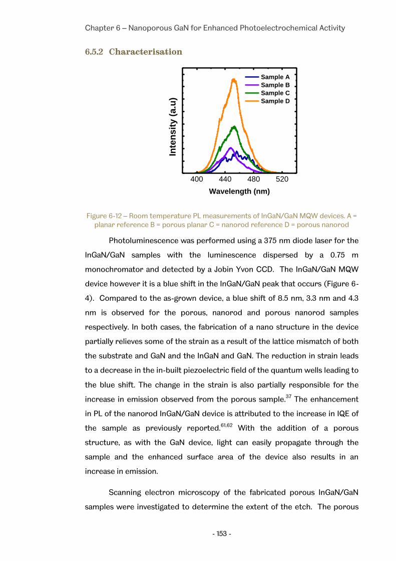
Chapter 6 – Nanoporous GaN for Enhanced Photoelectrochemical Activity
- 153 -
6.5.2 Characterisation
400 440 480 520
Wavelength (nm)
Sample A
Sample B
Sample C
Sample D
Inte
nsit
y (
a.u
)
Figure 6-12 – Room temperature PL measurements of InGaN/GaN MQW devices. A = planar reference B = porous planar C = nanorod reference D = porous nanorod
Photoluminescence was performed using a 375 nm diode laser for the
InGaN/GaN samples with the luminescence dispersed by a 0.75 m
monochromator and detected by a Jobin Yvon CCD. The InGaN/GaN MQW
device however it is a blue shift in the InGaN/GaN peak that occurs (Figure 6-
4). Compared to the as-grown device, a blue shift of 8.5 nm, 3.3 nm and 4.3
nm is observed for the porous, nanorod and porous nanorod samples
respectively. In both cases, the fabrication of a nano structure in the device
partially relieves some of the strain as a result of the lattice mismatch of both
the substrate and GaN and the InGaN and GaN. The reduction in strain leads
to a decrease in the in-built piezoelectric field of the quantum wells leading to
the blue shift. The change in the strain is also partially responsible for the
increase in emission observed from the porous sample.37 The enhancement
in PL of the nanorod InGaN/GaN device is attributed to the increase in IQE of
the sample as previously reported.61,62 With the addition of a porous
structure, as with the GaN device, light can easily propagate through the
sample and the enhanced surface area of the device also results in an
increase in emission.
Scanning electron microscopy of the fabricated porous InGaN/GaN
samples were investigated to determine the extent of the etch. The porous

Chapter 6 – Nanoporous GaN for Enhanced Photoelectrochemical Activity
- 154 -
InGaN/GaN MQW sample shown in Figure 6-11 (a) & (b) clearly shows some
variation in the extent of etching across the surface. Due to the structure of
the wafer, with an upper p-GaN layer, the etching across the surface takes
longer to occur than with n-GaN. This causes considerably smaller pores in
the upper layer compared to planar n-GaN as observed in Figure 6-4 despite
similar etch conditions. However, once an area is etched, the underlying
layers comprised of the InGaN/GaN MQW layers are etched at a faster rate,
resulting in the larger pores visible in Figure 6-11 (b). The distribution of the
more severe etching is sporadic, resulting in partial exposure of the quantum
wells. Despite this, the porous structure observed will still result in increased
contact of the quantum wells with the electrolyte solution decreasing the
required carrier diffusion length.
Figure 6-13 – SEM images of porous InGaN/GaN MQW structures (a) & (b) porous InGaN/GaN, Sample B (c) Reference InGaN/GaN nanorods, Sample C (d) & (e)
porous InGaN/GaN nanorods, Sample D
The nanorod samples are shown in Figure 6-11 (c)-(e). The nanorods
have a diameter of 200 nm and a density of 108 cm-2. After the nanorods are
PEC etched, the SEM only indicates a partial etching of the nanorods,
however the base of the sample is quite severely etched. As with the planar
device and observed in the nanorods in Chapter 5, the quantum wells in the
nanorods are partially etched. The variation in etch is due to the migration of

Chapter 6 – Nanoporous GaN for Enhanced Photoelectrochemical Activity
- 155 -
the carriers within the nanorod and planar structure resulting in the
oxidation occurring at the QW and n-GaN.
6.5.3 Solar Hydrogen Performance
-1 0 1 2
0.0
0.1
0.2
0.3
0.4
0.5
0.6
Cu
rren
t D
en
sit
y (
mA
cm
-2)
Voltage (V vs VCE
)
Sample A
Sample B
Sample C
Sample D
Figure 6-14 – Photocurrent measurements as a function of bias for InGaN/GaN MQW samples in 1M HCl and 1 sun illumination
The performances of the InGaN/GaN devices were investigated in a 1 M
HCl solution and 1 sun illumination (Figure 6-12). As observed with previous
devices, the fabrication of the nanorod structure leads to an increase in the
photocurrent of the device in comparison to the as-grown device. The
nanorod structure results in a photocurrent increase of 22 % after a bias is
applied. The porous structure however causes a significantly greater change
in photocurrent in both the planar and nanorod porous devices. As visible
from the SEM (Figure 6-11) the porous device exposes a significantly larger
area to the electrolyte resulting in the remarkable increase in photocurrent
observed from Sample B and Sample D. Device performance increases from
0.18 % for the as-grown to 0.26 % and 0.48 % for Sample B and D respectively.
Hydrogen Measurements
Assessment of the Sample A and B for hydrogen performance was
conducted under standard conditions (Figure 6-13). Theoretical and
measured values for the planar and porous sample illustrate a high faradic
efficiency with a strong agreement between the measurements. As expected
based on the photocurrent measurements the porous sample produces a

Chapter 6 – Nanoporous GaN for Enhanced Photoelectrochemical Activity
- 156 -
significantly higher volume of hydrogen than the planar device. Hydrogen
volumes for each sample are 0.25 ml hour-1 and 0.7 ml hour-1 for the
reference and nanoporous samples respectively, over a two fold increase in
production. This increase is due to the improved device efficiency and the
better adsorption and desorption properties of the porous structure.
0 10 20 30 40 50 600.0
0.1
0.2
0.3
0.4
0.5
0.6
0.7
0.8
Sample A
Sample B
Hyd
rog
en
Vo
lum
e (
ml)
Time (minutes)
Theoretical
Figure 6-15 – Hydrogen generation measurements of reference InGaN/GaN sample (A) and porous InGaN/GaN sample (B) in 1 M HCl at 0.8 V and 500 mW cm-2 Xe lamp
illumination. Lines indicate theorectical maximum.
Incident Photon Conversion Efficiency
IPCE measurements under standard conditions for the four samples
are presented in Figure 6-14. Compared to the n-GaN data in Figure 6-9, as a
result of the quantum wells the absorption of the device is extended to 440
nm with the peak efficiency of 11.9 % around the GaN band edge of 358 nm.
Fabrication of the nanorod structure enhances the emission across all
wavelengths with a peak of 42 % at 356 nm. The nanorod structure allows for
a better absorption of light within the quantum wells and enhances the
extraction of carriers due to the improved contact with the electrolyte.
Comparatively, the porous devices, B and D, have a better efficiency within
the GaN, with peak performance at the band edge of 46.6 % and 56.5 %
respectively. However, due to the etching of the InGaN quantum wells, the
efficiency at extended wavelengths is reduced when compared to the
unetched counterparts. This is as a result of the removal of areas with high
indium contents observed in other samples.52

Chapter 6 – Nanoporous GaN for Enhanced Photoelectrochemical Activity
- 157 -
350 400 580 6000
20
40
60
80
100
Wavelength (nm)
Sample A
Sample B
Sample C
Sample D
IPC
E (
%)
Figure 6-16 – Incident Photon Conversion Efficiency of InGaN/GaN reference Samples A and C and porous InGaN/GaN devices Samples B and D
6.5.4 Summary
As with the GaN samples, porous structures have been fabricated via a
PEC etch on InGaN/GaN wafers. As a result of the increased separation of the
charge carriers and greater surface area the photocurrent of the device is
enhanced. The novel structure also increases the hydrogen generation rate
of the device. Optimisation of the fabrication conditions could lead to further
improvements in the performance of the device. The minority carrier
diffusion length of indium gallium nitride can be as small as 30 nm. If the pore
structure of the MQW device can be optimised to allow for maximum
diffusion of carriers, recombination can be reduced enhancing the
performance of the device. Furthermore, specific control of the etch needs
to be conducted to minimise the loss of the indium in the quantum wells and
the reduction in IPCE at longer wavelengths visible in these samples.
6.6 Conclusions
Utilising a simple photoelectrochemical etch, porous devices have
been fabricated on III-nitride devices. Control over the etch can be achieved
by altering the concentration and voltage during the etch. Porous
nanostructures of GaN based devices have also been fabricated for the first
time resulting to an increase in the solar hydrogen performance of the
devices. IPCE measurements also show increases in the fabricated porous

Chapter 6 – Nanoporous GaN for Enhanced Photoelectrochemical Activity
- 158 -
structures with quantum well structures extending the optical absorption
compared to GaN. The use of nanostructures enhances the absorption of the
quantum wells increasing the potential performance of devices with higher
indium content quantum wells. Furthermore, the addition of NiO on the
porous samples has also been demonstrated as a potential solution for
further enhancements in photocurrent and as a preventative measure to
prolong the life of the device.

Chapter 6 – Nanoporous GaN for Enhanced Photoelectrochemical Activity
- 159 -
Bibliography
1 V. Kochergin and H. Foll, Porous Semiconductors: Optical Properties and Applications, Illustrate (Springer-Verlag, London, UK, 2009), p. 216.
2 E.B. Hensley, J. Appl. Phys. 23, 1122 (1952).
3 H. Föll, J. Carstensen, and S. Frey, J. Nanomater. 2006, 1 (2006).
4 K. Sayama, A. Nomura, T. Arai, T. Sugita, R. Abe, M. Yanagida, T. Oi, Y. Iwasaki, Y. Abe, and H. Sugihara, J. Phys. Chem. B 110, 11352 (2006).
5 Y. Ling, G. Wang, D. a Wheeler, J.Z. Zhang, and Y. Li, Nano Lett. 11, 2119 (2011).
6 M. Sathish, B. Viswanathan, and R. Viswanath, Int. J. Hydrogen Energy 31, 891 (2006).
7 Y.H. Ng, A. Iwase, A. Kudo, and R. Amal, J. Phys. Chem. Lett. 1, 2607 (2010).
8 P. Hartmann, D.-K. Lee, B.M. Smarsly, and J. Janek, ACS Nano 4, 3147 (2010).
9 B.D. Alexander, P.J. Kulesza, I. Rutkowska, R. Solarska, and J. Augustynski, J. Mater. Chem. 18, 2298 (2008).
10 J. Brillet, M. Grätzel, and K. Sivula, Nano Lett. 10, 4155 (2010).
11 H.M. Chen, C.K. Chen, R.-S. Liu, L. Zhang, J. Zhang, and D.P. Wilkinson, Chem. Soc. Rev. 41, 5654 (2012).
12 J. Zhu and M. Zäch, Curr. Opin. Colloid Interface Sci. 14, 260 (2009).
13 Y. Lin, G. Yuan, R. Liu, S. Zhou, S.W. Sheehan, and D. Wang, Chem. Phys. Lett. 507, 209 (2011).
14 H. Föll, S. Langa, J. Carstensen, M. Christophersen, and I.M. Tiginyanu, Adv. Mater. 15, 183 (2003).
15 S. Chattopadhyay, A. Ganguly, K.-H. Chen, and L.-C. Chen, Crit. Rev. Solid State Mater. Sci. 34, 224 (2009).
16 D. Zhuang and J.H. Edgar, Mater. Sci. Eng. R Reports 48, 1 (2005).
17 C. Youtsey, I. Adesida, and G. Bulman, Electron. Lett. 33, 245 (1997).
18 J.E. Borton, C. Cai, M.I. Nathan, P. Chow, J.M. Van Hove, A. Wowchak, and H. Morkoç, Appl. Phys. Lett. 77, 1227 (2000).

Chapter 6 – Nanoporous GaN for Enhanced Photoelectrochemical Activity
- 160 -
19 P. Visconti, K.M. Jones, M. a. Reshchikov, R. Cingolani, H. Morkoc ̧, and R.J. Molnar, Appl. Phys. Lett. 77, 3532 (2000).
20 M. Mynbaeva and D. V. Tsvetkov, Institue Phys. Conf. Ser. 155, 365 (1997).
21 M. Mynbaeva, a. Titkov, a. Kryganovskii, V. Ratnikov, K. Mynbaev, H. Huhtinen, R. Laiho, and V. Dmitriev, Appl. Phys. Lett. 76, 1113 (2000).
22 I.M. Huygens, K. Strubbe, and W.P. Gomes, J. Electrochem. Soc. 147, 1797 (2000).
23 X. Li, Y.-W. Kim, P.W. Bohn, and I. Adesida, Appl. Phys. Lett. 80, 980 (2002).
24 F.K. Yam, Z. Hassan, L.S. Chuah, and Y.P. Ali, Appl. Surf. Sci. 253, 7429 (2007).
25 K. Al-Heuseen, M.R. Hashim, and N.K. Ali, Appl. Surf. Sci. 257, 6197 (2011).
26 H. Hartono, C.B. Soh, S.J. Chua, and E. a. Fitzgerald, Phys. Stat. Sol (B) 244, 1793 (2007).
27 S.F. Cheah, S.C. Lee, S.S. Ng, F.K. Yam, H. Abu Hassan, and Z. Hassan, Appl. Phys. Lett. 102, 101601 (2013).
28 C. Youtsey, G. Bulman, and I. Adesida, J. Electron. Mater. 27, 282 (1998).
29 C. Youtsey, I. Adesida, and G. Bulman, Appl. Phys. Lett. 71, 2151 (1997).
30 C. Youtsey, I. Adesida, L.T. Romano, and G. Bulman, Appl. Phys. Lett. 72, 560 (1998).
31 C. Youtsey, L.T. Romano, and I. Adesida, Appl. Phys. Lett. 73, 797 (1998).
32 R. Radzali, N. Zainal, F.K. Yam, and Z. Hassan, Mater. Sci. Semicond. Process. 16, 2051 (2013).
33 S.Y. Bae, H.W. Seo, J. Park, H. Yang, and B. Kim, Chem. Phys. Lett. 376, 445 (2003).
34 C.B. Soh, C.B. Tay, R.J.N. Tan, A.P. Vajpeyi, I.P. Seetoh, K.K. Ansah-Antwi, and S.J. Chua, J. Phys. D. Appl. Phys. 46, 365102 (2013).
35 M. Ali, O. Svensk, L. Riuttanen, M. Kruse, S. Suihkonen, A.E. Romanov, P.T. Törmä, M. Sopanen, H. Lipsanen, M.A. Odnoblyudov, and V.E. Bougrov, Semicond. Sci. Technol. 27, 082002 (2012).
36 H.-W. Huang, J.T. Chu, C.C. Kao, T.H. Hseuh, T.C. Lu, H.C. Kuo, S.C. Wang, and C.C. Yu, Nanotechnology 16, 1844 (2005).

Chapter 6 – Nanoporous GaN for Enhanced Photoelectrochemical Activity
- 161 -
37 C.-F. Lin, J.-H. Zheng, Z.-J. Yang, J.-J. Dai, D.-Y. Lin, C.-Y. Chang, Z.-X. Lai, and C.S. Hong, Appl. Phys. Lett. 88, 083121 (2006).
38 K. Kim, J. Choi, T.S. Bae, M. Jung, and D.H. Woo, Jpn. J. Appl. Phys. 46, 6682 (2007).
39 A. Ramizy, Z. Hassan, and K. Omar, Sensors Actuators B Chem. 155, 699 (2011).
40 F.K. Yam, Z. Hassan, and A.Y. Hudeish, Thin Solid Films 515, 7337 (2007).
41 K. Al-Heuseen and M.R. Hashim, Sensors Actuators B Chem. 163, 159 (2012).
42 C.K. Inoki, T.S. Kuan, C.D. Lee, A. Sagar, R.M. Feenstra, D.D. Koleske, D.J. Díaz, P.W. Bohn, and I. Adesida, J. Electron. Mater. 32, 855 (2003).
43 R.S.Q. Fareed, V. Adivarahan, C.Q. Chen, S. Rai, E. Kuokstis, J.W. Yang, M.A. Khan, J. Caissie, and R.J. Molnar, Appl. Phys. Lett. 84, 696 (2004).
44 A.P. Vajpeyi, S. Tripathy, S.J. Chua, and E. a. Fitzgerald, Phys. E Low-Dimensional Syst. Nanostructures 28, 141 (2005).
45 J. a. Bardwell, J.B. Webb, H. Tang, J. Fraser, and S. Moisa, J. Appl. Phys. 89, 4142 (2001).
46 J.L. Weyher, L. Macht, F.D. Tichelaar, H.W. Zandbergen, P.R. Hageman, and P.K. Larsen, Mater. Sci. Eng. B 91-92, 280 (2002).
47 H.-Y. Lee, X.-Y. Huang, and C.-T. Lee, J. Electrochem. Soc. 155, H707 (2008).
48 X.Y. Guo, T.L. Williamson, and P.W. Bohn, Solid State Commun. 140, 159 (2006).
49 S.-W. Ryu, Y. Zhang, B. Leung, C. Yerino, and J. Han, Semicond. Sci. Technol. 27, 015014 (2012).
50 J.L. Weyher, F.D. Tichelaar, H.W. Zandbergen, L. Macht, and P.R. Hageman, J. Appl. Phys. 90, 6105 (2001).
51 A.M. Basilio, Y.-K. Hsu, W.-H. Tu, C.-H. Yen, G.-M. Hsu, O. Chyan, Y. Chyan, J.-S. Hwang, Y.-T. Chen, L.-C. Chen, and K.-H. Chen, J. Mater. Chem. 20, 8118 (2010).
52 M. Li, W. Luo, B. Liu, X. Zhao, Z. Li, D. Chen, T. Yu, Z. Xie, R. Zhang, and Z. Zou, Appl. Phys. Lett. 99, 112108 (2011).
53 F.K. Yam, Z. Hassan, and S.S. Ng, Thin Solid Films 515, 3469 (2007).

Chapter 6 – Nanoporous GaN for Enhanced Photoelectrochemical Activity
- 162 -
54 D.G. Zhao, S.J. Xu, M.H. Xie, S.Y. Tong, and H. Yang, Appl. Phys. Lett. 83, 677 (2003).
55 K. Al-heuseen, M.R. Hashim, and N.K. Ali, Phys. B Condens. Matter 405, 3176 (2010).
56 W.-H. Tu, Y.-K. Hsu, C.-H. Yen, C.-I. Wu, J.-S. Hwang, L.-C. Chen, and K.-H. Chen, Electrochem. Commun. 13, 530 (2011).
57 B. AlOtaibi, M. Harati, S. Fan, S. Zhao, H.P.T. Nguyen, M.G. Kibria, and Z. Mi, Nanotechnology 24, 175401 (2013).
58 S.H. Abud, Z. Hassan, and F.K. Yam, Int. J. Electrochem. Sci. 7, 10038 (2012).
59 S.H. Abud, Z. Hassan, and F.K. Yam, Mater. Lett. 107, 367 (2013).
60 M. Godlewski, E. Łusakowska, E.. Goldys, M.. Phillips, T. Böttcher, S. Figge, D. Hommel, P. Prystawko, M. Leszczynski, I. Grzegory, and S. Porowski, Appl. Surf. Sci. 223, 294 (2004).
61 Q. Wang, J. Bai, Y.P. Gong, and T. Wang, J. Phys. D. Appl. Phys. 44, 395102 (2011).
62 J. Bai, Q. Wang, and T. Wang, Phys. Stat. Sol (A) 209, 477 (2012).
Chapter 7 – Conclusion
- 163 -
Chapter 7
Conclusion
he fabrication of III-nitrides for solar hydrogen production is an
area of growing interest. In the previous chapters I have
undertaken a progressive approach to create novel nanostructures of GaN
and InGaN/GaN wafers to further enhance and improve upon the research
surrounding this topic.
7.1 Overview
The effects of climate change are being felt globally and the
restrictions on governments and industries to curb carbon emissions means
that green technologies are required. The use of hydrogen as a fuel source
and fuel store is not new, however current production methods are
unsatisfactory if the positive benefits of hydrogen as a clean fuel is to be
realised. Solar production of hydrogen is a viable technology to produce the
vast quantities of hydrogen that will be required if wide scale change is to
occur.1 Current material systems do not achieve the required lifetime or
efficiency required to achieve commercialisation. For effective water
splitting, the material is required to have specific properties, including the
band gap, band positions and stability under operating conditions. III-nitride
materials have the potential to achieve all three due to the tuneable band gap
of the alloys, the correct conduction and valence band positions and a strong
T
Chapter 7 – Conclusion
- 164 -
resistance to corrosion in chemical solutions. Despite this, prior to the start
of this research, the number of studies on III-nitride materials for
photoelectrochemical water splitting were limited.
The focus of previous research was mainly on as-grown planar
materials or intensively grown nanostructures limiting their practical
applicability. Over the course of this research, there has been an increased
focus on the possibility of using III-nitrides for water splitting and other
photoelectrochemical reactions. The aim of this thesis was to develop novel
approaches to the fabrication of III-nitride devices for solar hydrogen
production to increase the efficiency and overall performance of the material.
Throughout the previous chapters, examples on how this can be achieved
have been demonstrated though novel techniques previously unused within
the III-nitride material class for water splitting applications.
Chapter 4 demonstrated the fabrication of nanorods via the use of a
simple post growth fabrication technique which resulted in a significant
enhancement in photocurrent and hydrogen production. This was the first
time a nanorod structure had been fabricated from an MOCVD grown wafer
and investigated for its potential in water splitting. The method was
demonstrated to work with GaN and InGaN materials with enhancement
factors up to 6 achieved. This is due to the increased surface area obtained
through the creation of a nanorod array as well as reduced carrier
recombination due to the decrease in required path lengths. Optimisation of
the fabrication method has resulted in a high level of control over the
nanorods, creating structures that allow for the diffusion lengths of the
electrons and holes within the material. Due to the differences in diffusion
lengths of the III-nitride materials, the ability to control the nanorod size
effectively is important to achieve the optimum results for each alloy utilised.
Measurements of hydrogen evolution of the nanorod array also validated the
improved device performance with a strong faradaic performance and
significant increase over the reference planar device.

Chapter 7 – Conclusion
- 165 -
Realisation into the potential for increased corrosion of the nanorod
device due to the device structure prompted the research discussed in
Chapter 5. Device longevity is essential for it to be cost effective and
commercial viable. The use of cocatalysts is widespread in the desire to
achieve high rates of hydrogen evolution however the work on GaN was
limited. NiO nanoparticles had been utilised on planar devices, however the
mechanism and understanding behind their positive effect was not well
understood. Through the deposition of NiO nanoparticles onto the nanorod
array structures that had been developed in Chapter 4 a significant
enhancement in their lifetime and photocurrent has been achieved. Further
to this, the investigation into the understanding of process in regards to
reaction sites and band positions has added to the previous research and
knowledge of the community. The enhancement in photocurrent is
attributed to the conduction and valence band positions of the NiO. Due to
their complementary position compared to GaN and III-nitride materials the
separation of photogenerated carriers is enhanced. The higher conduction
band of NiO prevents electron flow to the surface while the valence band
position promotes hole flow. As a result, recombination within the bulk
material is reduced increasing photocurrent. The improvement in device
lifetime is a result of the hole migration. Due to the corrosion of GaN through
the reaction of holes at the surface reducing the number of surface reactions
prevents the rate of corrosion of the electrode. The NiO acts as the reaction
site for oxygen evolution preventing photocorrosion.
Identification of photocorrosion of GaN resulted in the work
conducted in Chapter 6. Nanostructures had already been identified as a
positive technique to enhance the performance of a device and therefore the
creation of a porous structure could further improve this. Previous research
had identified the use of etching techniques and surface treatments to
improve photocurrents however photoelectrochemical etching of GaN had
only yielded detrimental effects. The use of a potassium hydroxide solution,
voltage and illumination source have been shown to create a porous
structure in the GaN and InGaN/GaN materials. By varying the conditions of
Chapter 7 – Conclusion
- 166 -
the technique a level of control in regards to pore size and etch depth has
been achieved. An enhancement in photocurrent was observed for all porous
devices which contradicted previous research. The chemical treatment
created a network of pores that increased the total surface area of the device
as well as reducing the distances required for minority diffusion. The use of
the porous structure demonstrated similar benefits to that of the nanorod
array due to the properties of nanostructured semiconductors. Optimum
fabrication conditions for porous GaN were achieved and investigated
through SEM and photocurrent measurements. Alongside the development
of porous GaN, porous InGaN/GaN quantum well devices were fabricated and
studied. Prior to this work, the use of porous InGaN/GaN had not been
identified as a potential option for water splitting.
Further to this, the individual techniques developed during this thesis
were combined to create a highly ordered nanorod array with porous cavities
and porous devices with NiO nanoparticles. Control over both techniques
resulted in further enhancements to the photocurrent and hydrogen
evolution. The addition of NiO nanoparticles to the porous devices also
resulted in a similar enhancement and improvement in corrosion prevention
demonstrated with the nanorod array. By combining each of the techniques
developed in this research an enhancement in photocurrent, hydrogen
production and device lifetime has been achieved. These three areas are
significant requirements for the development of high quality electrodes for
water splitting.
7.2 Future Research
The focus of this thesis has been on GaN and InGaN/GaN quantum well
devices. Enhancements in performance through the fabrication of novel
nanostructures has been achieved however there is the potential for further
work to be conducted to attain the high photocurrents required for
commercial application. Due to the nature of GaN and InGaN, the techniques
utilised in this work can potentially be applied to the entire alloy range of the
III-nitride materials.

Chapter 7 – Conclusion
- 167 -
7.2.1 InGaN bulk films
The incorporation of indium into gallium nitride is essential if the band
gap is to be reduced to the required level of 1.8 eV.2 Although the use of
quantum wells allows the growth of high indium content films there are
potential issues. In order to achieve sufficient absorption of visible radiation
a film thickness of at least 100 nm is required. Typical quantum wells are <10
nm and therefore the majority of input energy will be lost. The use of bulk
InGaN wafers can increase the amount of solar radiation available significantly
from the 2 % of GaN. Bulk InGaN films and MBE grown InGaN nanostructures
have been investigated,3,4 however there are currently no studies in which the
fabrication techniques developed in this thesis are utilised to create InGaN
nanostructures from MOCVD grown material. Due to the extensive
development of the technique on GaN, implementation into a bulk InGaN
should be easily obtainable which could potentially result in device
efficiencies higher than currently reported.
7.2.2 Intermediate Bands
Another potential opportunity to expand the absorption of GaN based
devices is through the incorporation of intermediate bands.5 Some
preliminary work on manganese doped GaN on top of n-type GaN have
identified the potential of intermediate bands in III-nitrides for water
splitting.6 The principle behind intermediate bands is the addition of a band
within the main band of the bulk material. The addition of this band allows for
absorption of sub band gap photons resulting in the potential for two photon
absorption. This could be specifically useful for GaN in which the absorption
of visible light is the main factor contributing to the lower performance. Due
to ability to create semiconductors with band gaps varying from 0.7 eV
through to 3.4 eV by alloying different types of indium with GaN, it is possible
to create a complementary system with of the same material type. This
means that the requirements of crystal matching to prevent low quality
growth is minimised. If multiple intermediate bands are located within the
GaN band it is possible that the absorption can be shifted significantly from
the UV through to the infrared. Combining intermediate bands with the

Chapter 7 – Conclusion
- 168 -
nanostructures could significantly enhance the efficiency of the
photoelectrode.
7.2.3 Device Properties
The fabrication of the device is only one aspect that plays a role in the
overall performance. The extraction of carriers from the device is essential if
high photocurrents are to be achieved. One method in which this could be
achieved is through the optimisation of the ohmic contact on the device.
Through the use of multiple finger contacts as opposed to a single contact
improvements in photocurrents have been observed for both n- & p-type
GaN.7,8 The fabrication of these structures is relatively straight forward for
planar devices however, due to the use of nanostructured GaN and InGaN,
increasing the complexity of the contact can cause additional problems.
Therefore, optimisation of the fabrication of more complex contacts for
increased majority carrier extraction is required for the nanostructured
devices fabricated in this thesis.
7.2.4 Summary
The potential for the furthering of this research is relatively vast. Due
to the early nature of the research on III-nitrides for water splitting there is
the opportunity to develop the variety of approaches discussed. Each
technique could potentially increase the efficiency of the device and through
the implementation of the fabrication techniques to create nanostructures.
Due to the nature of the fabrication methods, the main requirement for
improvement in GaN based devices is through the optimisation of the growth
techniques to achieve high quality wafers. If this is achieved, the
implementation of the techniques developed in this research can be easily
applied leading to substantial gains in device efficiencies for implementation
in green technology.

Chapter 7 – Conclusion
- 169 -
Bibliography
1 M. Grätzel, Nature 414, 338 (2001).
2 P.G. Moses and C.G. Van de Walle, Appl. Phys. Lett. 96, 021908 (2010).
3 K. Aryal, B.N. Pantha, J. Li, J.Y. Lin, and H.X. Jiang, Appl. Phys. Lett. 96, 052110 (2010).
4 W. Luo, B. Liu, Z. Li, Z. Xie, D. Chen, Z. Zou, and R. Zhang, Appl. Phys. Lett. 92, 262110 (2008).
5 L. Cuadra, a Martı ́, and a Luque, Thin Solid Films 451-452, 593 (2004).
6 S.-Y. Liu, J.K. Sheu, Y.-C. Lin, S.J. Tu, F.W. Huang, M.L. Lee, and W.C. Lai, Opt. Express 20 Suppl 5, A678 (2012).
7 S.-Y. Liu, J.K. Sheu, M.L. Lee, Y.-C. Lin, S.J. Tu, F.W. Huang, and W.C. Lai, Opt. Express 20 Suppl 2, A190 (2012).
8 S.-Y. Liu, J.K. Sheu, C.-K. Tseng, J.-C. Ye, K.H. Chang, M.L. Lee, and W.C. Lai, J. Electrochem. Soc. 157, B266 (2010).