novel enhancement techniques for ultra-high-performance...
TRANSCRIPT

Novel Enhancement Techniques for Ultra-High-Performance Conformal Wireless Sensors and "Smart Skins" Utilizing Inkjet-Printed Graphene
Taoran Le, Ziyin Lin, C. P. Wong, and M. M. Tentzeris
Georgia Institute of Technology, Atlanta, GA [email protected]
Abstract We introduce various novel techniques for the performance
enhancement of nanotechnology-enabled wireless platforms utilizing inkjet-printed graphene thin films, especially for gas sensing applications in this paper. Compared to previously reported results (6% sensitivity after exposure to 500 ppm NH3), we have improved the performance by nearly a factor of 10, increasing the sensitivity to 4.8% at 60 ppm. Key advancements to the reduced graphene oxide (rGO) thin film include: (i) drastically reduced (micron to nm) film thickness via surface modification techniques, specifically enhancing charge transport properties, and (ii) increased porosity obtained via a unique in-house developed nano-patterning process. The proposed graphene-based thin film approach could set the foundation for a plethora of novel wireless sensing and gas-reconfigurable communication platforms. Introduction Currently, sensing and wireless technologies are becoming more pervasive and inter-tangled with continuous breakthroughs, especially after the introduction of nanostructures, such as carbon nanotubes (CNTs) and graphene. One of the major topics of substantial interest is the development of techniques to produce low-cost, scalable, robust wireless sensors and reconfigurable communication modules. The integration techniques using nano-materials becomes one of the critical pieces during the fabrication process. Recently, material science advances have led to some extremely novel and interesting possibilities [1-3]. Meanwhile, the use of inkjet printing techniques for the development of graphene thin films as a sensing medium, and their integration into wireless sensor nodes has been reported [4,5]. Based on our previous efforts, we have identified several key areas of exploration for enhancement of the performance of the wireless platforms utilizing inkjet-printed graphene oxide (GO) thin films. In particular, this research focuses on improving the performance of novel gas sensors, with emphasis on film thickness, porosity, and uniformity. At the same time, a low-cost inkjet-printing fabrication process is utilized. Namely, the contributions of this paper include: 1) Surface Modification of the Substrate: Via proprietary
in-house developed processes, we enhance the substrate so that the graphene platelets bind to the surface in an even manner, approximately one molecule thick. This also greatly reduces the film thickness and increases the uniformity.
2) Ink Modification: The graphene oxide (GO) ink is modified corresponding to the surface preparation so that the individual graphene sheets bind strongly to the substrate medium, enhancing film strength and uniformity.
3) Nano-sphere Patterning of the Thin Film: Via nano-engineering of the thin film during processing, we are able to increase and control precisely the porosity of the thin film. We expect that the increased porosity will enhance the response to gas.
Overview of Surface Modification Based on our previous sensor work, we discovered that in
order to enhance the weak binding between the GO ink and substrate, the first improvement involves the enhancement of uniformity and reduction of the film thickness. For the purpose of producing the most uniform and ultra-thin carbon films, the in-house developed surface engineering process, which had been previously used to enhance the wettability of Si wafers, was utilized to prepare the flexible substrate (in this case – PET and Kapton) prior to GO ink deposition. After the surface modification, the wettability and printability of the GO ink on the substrate was dramatically improved. As a result, agglomerations and islanding effects can be avoided. And it became possible to inkjet print conformal, continuous, and ultra-thin (< 50 nm thickness) GO films on numerous substrates spanning from conventional Si wafer and glass to flexible substrates such as Kapton and PET.
The surface modification process consists of: (1) first applying a polymer coating with positively charged chemical groups (such as amine groups) to the surface of the substrate. (2) Then, through a well-established in-house process of layer-by-layer dendritic amplification, these groups are then amplified to the desired density (Fig. 1). The resulting substrate surfaces become densely positively charged and hydrophilic, and ready for conformal inkjet printing of the negatively charged and hydrophilic carbon-based nanomaterials.
Figure 1. Surface modification process to thin substrate.
978-1-4799-0232-3/13/$31.00 ©2013 IEEE 1640 2013 Electronic Components & Technology Conference

The opposite charges allow for a strong electrostatic force which attracts and bonds the graphene platelets in exactly the desired pattern. Combining this process with lithographic techniques, the resolution of the printing process can be down to several um (<5 um) for the purpose of inkjet printing graphene traces for electrical circuits on virtually any surface ranging from organics to glass and silicon wafers. Figure 2 demonstrates the effect of surface treatment and GO ink on Kapton.
Figure 2. Inkjet printing of highly porous carbon-based nanomaterials on a surface modified Kapton
Graphene Oxide Ink "Match" After we modify the substrate, we also tune the ink to
“match” the substrate. This process involves surface modifying the nanomaterial (in this case GO) to be terminated with dense negative charges so that they can readily bind to the positively charged substrate patterning via electrostatic interaction during inkjet printing. This can be easily achieved by the introduction of surface carboxyl groups on the carbon nanomaterials with well-developed carbon chemistry.
In addition to tuning the nanoparticles, we must also balance the surface energy between the substrate and the ink in order to minimize the surface energy difference, so that the ink particles can be uniformly dispersed on the substrate and allow binding to occur uniformly. This can be accomplished by selecting appropriate solvents, tuning the viscosity and density of the inks, etc.
Nano Patterning Technique The surface areas of the carbon-based nanomaterials are
critical to their sensitivity to chemical and biological agents. In order to develop highly porous thin films of carbon nanomaterials, we utilized a novel technique that creates nanoscale pores in the thin films via the introduction and selective dissolution of commercially available, low-cost polymer nanospheres made of poly(methyl methacrylate) (PMMA) or polysterene.
Briefly, the GO and polymer nanospheres were surface modified separately to bear dense opposite charges - for example, GO was positively charged (terminated with amine groups) and polymer nanospheres were negatively charged (terminated with carboxyl groups) - and then mixed to let the polymer nanospheres bind to the carbon nanomaterials via electrostatic interaction. Water-based inks were then created
from the nanosphere-bound GO and the viscosity of the resulting suspension was adjusted to optimize their printability on a Dimatix DMP-2800 inkjet printer. After drying, the printed thin films were sequentially incubated first with acetone and then with toluene to selectively remove the polymer nanospheres, leaving the GO thin film and substrate unaffected (see Figure 3). to these analytes.
Figure 3. Inkjet printing of highly porous carbon-based nanomaterials on a surface modified flexible substrate.
Figure 4. A). SEM image of a graphene oxide-polystyrene thin film printed on surface modified PET substrate (5 passes) after the
selective removal of polymer nanospheres; B). SEM image of a GO thin film printed with the absence of nanospheres in the ink.
After the reduction process, the resulting highly porous rGO thin films can be further engineered for enhanced sensitivity and/or selectivity. Figure 4 shows the morphological difference between inkjet printed graphene oxide thin films on PET substrate. Figure 4A shows a SEM image of the film utilizing the nanosphere patterning technique; 4B shows the standard film without nano-engineering. As illustrated, the GO thin film, which has been patterned, is substantially more porous compared to the standard (non-patterned) film.
In this experiment, ~50 nm polystyrene nanospheres were utilized and highly porous GO thin films were obtained upon selective removal of the nanospheres. It is possible to choose and optimize the nanosphere size. We note that high porosity of a thin film typically deteriorates its conductivity. We are currently making rapid progress in optimizing our ink formulation and printing conditions (changing the size of the polymer nanospheres and the thickness of the thin film, and tuning the ratio of GO to nanosphere nanoparticles) to obtain the best compromise between the conductivity and porosity of the printed rGO thin films. Soon, it will be possible to determine the exact process parameters to optimize the thin film impedance and sensitivity for a given application.
A B
1641

Raman Spectrum The Raman spectrum of graphitic structure can provide
important insights into its structure and stacking. Figure 5 shows the representative Raman spectra of thermally reduced GO, which were printed by 1 layer (Figure 5a) and 4 layers (Figure 5b).
Figure 5. Raman spectra of thermally reduced GO: (A) 1 layer (B) 4 layers.
Characteristic peaks for graphene are observed. The peak at ~ 1330 cm-1 is D peak which is defect-related, and the peak at ~1565 cm-1 is G peak which results from the graphitic structure. The intensity ratio of D peak and G peak (ID/IG) ratio can be used to study the structure of carbon-based materials. It is found that ID/IG ratio varies from 0.9 to 1.1 at different locations of sample and is not dependent on the number of printed layers. The peak at ~ 2700 cm-1 is called 2D peak, and can be used to study of the number of graphene layers. The strong 2D peak for thermally reduced 4-layer GO indicates a graphite-like stacking, whereas the weak 2D peak for thermally reduce 1-layer GO suggests a smaller thickness of printed layers.
Battery-less Wireless Sensing and Communication Platform
As in the previous work,we used the same WISP sensing and communication platform to test the improvement of the wireless sensor sensitivity [4]. The WISP is a battery-free, fully passive, and programmable RFID Tag [6], which can be powered, and read by off-the-shelf EPC Gen2 UHF RFID
Readers and has an on-board microcontroller for sensing and computing functions.
WISP is a flexible platform offering the reliability of wireless digital transmission. Our developed prototype WISP-GS (Gas Sensor) platform is shown in Fig. 6. The WISP-GS is solely powered by the RF energy illuminated by a very popular commercial RFID Reader. This 915MHz RF energy is rectified with its charge pump to charge the on-board capacitor. As soon as sufficient energy is accumulated and the voltage across the capacitor monitored by a supervisor exceeds the turn-on voltage of the MCU by an overhead margin, a regulated voltage of 1.805V is used to power both the MCU and our prototype external gas sensing board.
The external WISP-GS board consists of the inkjet-printed rGO sensor, presented in the previous section, as well as the analog interface of this sensor.
The analog interface is essentially a voltage divider, in which the voltage drop across the gas sensor module is directly tied to the resistance change of the sensor’s grapheme film pad and can easily be captured with the WISP’s integrated analog-to-digital converter (ADC) (pin 2.3). The resolution achieved can be defined by dividing the maximum resistance value by the 1024 discrete levels of the integrated 10-bit ADC, which gives approximately ± 1 mV accuracy.
Our modified WISP graphical user interface can report in real time the resistance of the rGO film that can be easily mapped to the real gas concentration with the extracted fitting equation, the sensor’s serial number and type, the total number of readings, the time it was last seen as well the full EPC Gen2 message transmitted. The report rate is only a few milliseconds, allowing for immediate reaction to health-threatening gas concentrations.
Results
A. Experimental Setup:
To test and validate the thin film enhancements, we examine the samples under gas test. The measurement setup and procedures used here are identical to the timing test given in [4,5]. We use a KIN-TEK FlexStream™ Gas Standards Generator gas generator to provide a stable gas source with accurate concentrations. The rGO thin film is placed in a
Figure 6. The WISP-GS (Gas Sensor) prototype platform
ADC Input
Graphene-based Inkjet-printed Gas Sensor
Regulated 1.8 V
A
B
1642
custom designed gas chamber under the gas test. The process consists of: 1) Placing samples in a custom enclosure and flowing pure
Nitrogen on the sample for 5 minutes to cleanse it. 2) Introducing the test gas (NH3 in this case) at the desired
concentration and beginning measurements every minute until near saturation condition is achieved.
B. Thin film Profile Reduction:
By use of the substrate modification, we were able to substantially reduce the thin film thickness. Table 1 below provides the results of the thickness measurements taken with a DekTak® profilometer for thin films consisting of 1-5 layers of reduced graphene oxide.
TABLE I
PROFILE MEASUREMENTS OF RGO THIN FILMS Layers 1 2 3 4 5
Thickness [nm]
54.0 93.3 144.8 202.0 245.1
Avg. Thickness per Layer
[nm]
54.0 46.7 48.3 50.5 49.0
Note that the average thickness per layer on the treated
substrate is only 49.67 nm. In previous efforts, at least 15-20 layers were required to achieve a conductive medium. Using the methods given here, we can obtain a conductive medium with just 1 layer. Therefore, we can print films as thin as 50 nm.
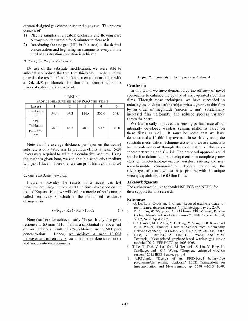
C. Gas Test Measurements:
Figure 7 provides the results of a recent gas test measurement using the new rGO thin films developed on the treated Kapton. Here, we will define a metric of performance called sensitivity S, which is the normalized resistance change as in
S=(Rgas - Rair) / Rair ×100%
Note that here we achieve nearly 5% sensitivity change in response to 60 ppm NH3. This is a substantial improvement on our previous result of 6%, obtained using 500 ppm concentration. Hence, we achieve a near 10-fold improvement in sensitivity via thin film thickness reduction and uniformity enhancements.
Figure 7. Sensitivity of the improved rGO thin film.
Conclusion In this work, we have demonstrated the efficacy of novel
approaches to enhance the quality of inkjet-printed rGO thin films. Through these techniques, we have succeeded in reducing the thickness of the inkjet-printed graphene thin film by an order of magnitude (micron to nm), substantially increased film uniformity, and reduced process variance across the board.
We dramatically improved the sensing performance of our internally developed wireless sensing platforms based on these films as well. It must be noted that we have demonstrated a 10-fold improvement in sensitivity using the substrate modification technique alone, and we are expecting further enhancement through the modification of the nano-sphere patterning and GO ink. The proposed approach could set the foundation for the development of a completely new class of nanotechnology-enabled wireless sensing and gas-reconfigurable communication devices combining the advantages of ultra low cost inkjet printing with the unique sensing capabilities of rGO thin films.
Acknowledgments The authors would like to thank NSF-ECS and NEDO for their support for this research. References 1. G. Lu, L. E. Ocola and J. Chen, “Reduced graphene oxide for
room-temperature gas sensors,” – Nanotechnology 20, 2009. 2. K. G. Ong, K. Zeng and C. A. Grimes, “A Wireless, Passive
Carbon Nanotube-Based Gas Sensor,” IEEE Sensors Jounal, Vol.2, No.2, April 2002.
3. J. D. Fowler, M. J. Allen, V. C. Tung, Y. Yang, R. B. Kaner and B. H. Weller, “Practical Chemical Sensors from Chemically Derived Graphene,” Acs Nano, Vol.3, No.2, pp.301-306. 2009.
4. T. Le, V. Lakafosi, Z. Lin, C.P. Wong, and M.M. Tentzeris, “Inkjet-printed graphene-based wireless gas sensor modules”2012 IEEE ECTC, pp.1003-1008.
5. T. Le, T, Thai, V. Lakafosi, M. Tentzeris, Z. Lin, Y. Fang, K. Sandhage, and C.P. Wong, “Graphene enhanced wireless sensors” 2012 IEEE Sensor, pp. 1-4.
6. A.P.Sample, “Design of an RFID-based battery-free programmable sensing platform,” IEEE Transactions on Instrumentation and Measurement, pp. 2608 ─2615, 2008.
1643