noninterleaved metasurface for (26‑1) spin- and wavelength ... · will be used to design...
TRANSCRIPT
Noninterleaved Metasurface for (26‑1) Spin- and Wavelength-Encoded HologramsLei Jin,† Zhaogang Dong,‡ Shengtao Mei,† Ye Feng Yu,§ Zhun Wei,† Zhenying Pan,‡,§
Soroosh Daqiqeh Rezaei,∥,‡ Xiangping Li,⊥ Arseniy I. Kuznetsov,‡,§ Yuri S. Kivshar,#
Joel K. W. Yang,*,∇,‡ and Cheng-Wei Qiu*,†
†Department of Electrical and Computer Engineering, National University of Singapore, 4 Engineering Drive 3, Singapore 117583,Singapore‡Institute of Materials Research and Engineering, A*STAR (Agency for Science, Technology and Research), 2 Fusionopolis Way,#08-03 Innovis, 138634 Singapore§Data Storage Institute, A*STAR (Agency for Science, Technology and Research), 2 Fusionopolis Way, #08-01 Innovis, 138634Singapore∥Department of Mechanical Engineering, Faculty of Engineering, National University of Singapore, 9 Engineering Drive 1, 117575,Singapore⊥Guangdong Provincial Key Laboratory of Optical Fiber Sensing and Communications, Institute of Photonics Technology, JinanUniversity, Guangzhou, 510632 China#Nonlinear Physics Centre, Australian National University, Canberra ACT 2601, Australia∇Singapore University of Technology and Design, 8 Somapah Road, 487372 Singapore
*S Supporting Information
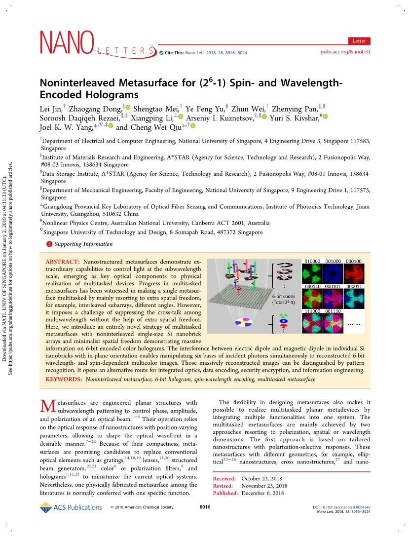
ABSTRACT: Nanostructured metasurfaces demonstrate ex-traordinary capabilities to control light at the subwavelengthscale, emerging as key optical components to physicalrealization of multitasked devices. Progress in multitaskedmetasurfaces has been witnessed in making a single metasur-face multitasked by mainly resorting to extra spatial freedom,for example, interleaved subarrays, different angles. However,it imposes a challenge of suppressing the cross-talk amongmultiwavelength without the help of extra spatial freedom.Here, we introduce an entirely novel strategy of multitaskedmetasurfaces with noninterleaved single-size Si nanobrickarrays and minimalist spatial freedom demonstrating massiveinformation on 6-bit encoded color holograms. The interference between electric dipole and magnetic dipole in individual Sinanobricks with in-plane orientation enables manipulating six bases of incident photons simultaneously to reconstructed 6-bitwavelength- and spin-dependent multicolor images. Those massively reconstructed images can be distinguished by patternrecognition. It opens an alternative route for integrated optics, data encoding, security encryption, and information engineering.
KEYWORDS: Noninterleaved metasurface, 6-bit hologram, spin-wavelength encoding, multitasked metasurface
Metasurfaces are engineered planar structures withsubwavelength patterning to control phase, amplitude,
and polarization of an optical beam.1−6 Their operation relieson the optical response of nanostructures with position-varyingparameters, allowing to shape the optical wavefront in adesirable manner.7−22 Because of their compactness, meta-surfaces are promising candidates to replace conventionaloptical elements such as gratings,14,18,19 lenses,11,20 structuredbeam generators,19,21 color6 or polarization filters,8 andholograms7,12,22 to miniaturize the current optical systems.Nevertheless, one physically fabricated metasurface among theliteratures is normally conferred with one specific function.
The flexibility in designing metasurfaces also makes itpossible to realize multitasked planar metadevices byintegrating multiple functionalities into one system. Themultitasked metasurfaces are mainly achieved by twoapproaches resorting to polarization, spatial or wavelengthdimensions. The first approach is based on tailorednanostructures with polarization-selective responses. Thesemetasurfaces with different geometries, for example, ellip-tical23−26 nanostructures, cross nanostructures,27 and nano-
Received: October 22, 2018Revised: November 25, 2018Published: December 6, 2018
Letter
pubs.acs.org/NanoLettCite This: Nano Lett. 2018, 18, 8016−8024
© 2018 American Chemical Society 8016 DOI: 10.1021/acs.nanolett.8b04246Nano Lett. 2018, 18, 8016−8024
Dow
nloa
ded
via
NA
TL
UN
IV O
F SI
NG
APO
RE
on
Janu
ary
2, 2
019
at 0
4:11
:33
(UT
C).
Se
e ht
tps:
//pub
s.ac
s.or
g/sh
arin
ggui
delin
es f
or o
ptio
ns o
n ho
w to
legi
timat
ely
shar
e pu
blis
hed
artic
les.

rods,28−31 can achieve dual functions depending on the inputpolarization, such as polarization beamsplitters,23 three-dimen-sional stereoscopic prints,24 double-wavelength meta-lens,26
and polarization-switchable holgorams.23,27,29,31 However,capabilities of these metasurfaces are limited by polarizationstates. To increase the capabilities, the extra spatial freedomswere exploited. The extra spatial freedoms included multiple
positions,32−34 multiple angles,34,35 and interleaved subarrays.For multiple positions or angles, metasurfaces controlled theincident beams to exhibits multifunctionality at differentpositions or angles, while interleaved was achieved either byvertical stacking36,37 or in-plane interleaving37−49 the subarraysspecifically designed for each functionality. On the basis of theextra spatial freedoms, metasurfaces are able to generate
Figure 1. Schematic diagram of the mechanism and unit cell structure. (a) The transmission-type 6-bit metasurface consists of silicon nanobricksarrays with spatially varying orientations on a quartz substrate. By manipulating six fundamental bases of the input beams, the designed meta-hologram is able to reconstruct 26-1 different color variations of an image. The 6-bit code of the incident beam is in the transmission 1 or blocking 0of the 3 × 2 (wavelength × spin) bases of the input light. The transmitted beams carry the embedded information on metasurface and reconstructthe corresponding images at the observation plane. The six fundamental bases (RRCP, GRCP, BRCP, RLCP, GLCP, and BLCP) of incident light areencoded by 100000, 010000, 001000, 000100, 000010, and 000001, respectively. The series si represent the varying states of incident beams andcorresponding states of reconstructed image. (b) Part of experimental reconstructions of 6-bit metasurface by each fundamental bases (C6
1), two outof six fundamental bases (C6
2), and three out of six fundamental bases (C63). (c) Geometry of the designed unit cell structure representing one pixel
in the meta-hologram with periodicity P = 350 nm. The silicon nanobrick is 50 nm wide, 300 nm long, and 150 nm high, which rotates in planewith an orientation angle θ. The silicon nanobricks with a rotating angle will introduce the geometric phase of ±2θ for opposite spins. (d) Scanningelectron microscopy (SEM) image of a partial region of the fabricated Si metasurface. Each Si nanobrick (300 nm × 50 nm) represents a phasepixel as defined in the metasurface (scale bar: 1 μm). The equivalent pixel size is 350 × 350 nm2. (e,f) Multipolar decomposition calculations of thescattering cross sections, σsca
L (e) and σscaS (f) with the superscripts denoting the polarization of the incident beam along long-axis (L) and short-axis
(S) of the nanobrick, respectively. Inset: Gray rectangles are the nanobricks and double arrows are the polarizations of incident beam. (g)Simulated and measured conversion efficiency. The conversion efficiency is defined as the ratio between the optical power of the transmitted lightwith opposite handedness and the incident optical power. The blue and black curves represent the simulated and experimentally measuredefficiency for amorphous Si nanobricks, respectively.
Nano Letters Letter
DOI: 10.1021/acs.nanolett.8b04246Nano Lett. 2018, 18, 8016−8024
8017

multimeta-hologram,32−34,42 full-color holograms,35,43,44,49 op-tical angular momentum (OAM) generators,38,39 OAMspectropolarimeter,40,41 optical recording,37 and achromaticlenses.36,46 Moreover, although wavelength dimension hasbeen exploited for multitasked metasurfaces, the cross-talksamong different wavelengths are mainly eliminated by specifictailored nanostructures,50 multiple angles,35 or interleavedsubarrays.43 −46 ,49 There is a lack of a convenient way tosuppress the cross-talk among multiwavelength without thehelp of extra spatial freedom.In this paper, we introduce a novel type of multitasked
metasurface with spin-wavelength encoding that allows 6-bit
control of incident beam based on minimalist spatial freedom(noninterleaved amorphous silicon nanobricks in an on-axissystem), which is capable of 6-bit encoding color holograms.Here we employ the concept of “bit” to describe thefundamental bases that reconstruct a multicolor image. Eachfundamental basis represents a monochromatic beam withpolarization. For a mixing beam formed by N fundamentalbases, each fundamental basis can be a unit vector in N-dimensional space being expressed by an N-bit digital code.Each fundamental basis has binary states, “extinction” and“existence”, corresponding to “0” and “1”, respectively. Toachieve the 6-bit for normal incidence, the red R, green G, and
Figure 2. Creation of wavelength- and spin-dependent meta-hologram. Two sets of hologram phase profiles, φRCP(x0,y0) and φLCP(x0,y0), are
designed to operate incident beams with opposite spins and merged together by the function Ae e ei x y i x y i x y( , ) ( , ) ( , )0 0 LCP 0 0 RCP 0 0= +φ φ φ . (a) Under theillumination of right-circularly polarized (RCP) light, the phase profile φRCP(x0,y0) reconstructs the holographic images R, G and B at theobservation Z0 plane by red, green, and blue beams, respectively. (b) Under the illumination of left-circularly polarized (LCP) light, the phaseprofile φLCP(x0,y0) reconstructs the holographic images flower, leaf, and snowflake at the observation Z0 plane by red, green, and blue beams,respectively. (c) The designed metasurface with merged phase profile φ(x0,y0) manipulates six fundamental bases to reconstruct six wavelength-and spin-dependent images at the observation Z0 plane. The six fundamental bases are in the transmission 1 or blocking 0 state.
Nano Letters Letter
DOI: 10.1021/acs.nanolett.8b04246Nano Lett. 2018, 18, 8016−8024
8018

blue B wavelengths with two different spins are used torepresent six fundamental bases (RRCP, GRCP, BRCP, RLCP, GLCP,and BLCP). The interference between electric dipole andmagnetic dipole in single-sized Si nanobricks with in-planerotation, that is, the Pancharatnam-Berry (PB) phase, enablescomplete 6-bit control of incident beams, which provides thedispersionless phase profile and spin-dependent tunability. Onthe basis of the dispersion relationship of propagation,46 themultiwavelength Gerchberg-Saxton (MWGS) algorithm wasused to retrieve two phase profiles: one phase profileφRCP(x0,y0) is designed to control RRCP, GRCP, BRCP toreconstruct independent images at a given z-plane; anotherone φLCP(x0,y0) is designed to control RLCP, GLCP, and BLCP toreconstruct independent images at the same plane. These twophase profiles are then combined together by the function
Ae e ei x y i x y i x y( , ) ( , ) ( , )0 0 LCP 0 0 RCP 0 0= +φ φ φ and encoded into a singlemetasurface according to PB phase. As a result, by controllingthe states of 6-bit coding incident beams, the designed 6-bitmetasurface is able to reconstruct 63 spin-and wavelength-dependent holographic images (as shown in Figure 1a,b). Thereconstructed images and corresponding incident beams canbe distinguished by employing pattern recognition. Thisapproach can be extended to design versatile wavelength-multiplexed planar optical devices for color display, opticalimaging, optical encryption, and data encoding.The phase-modulated 6-bit metasurface is constructed by a
set of amorphous Si subwavelength elements arranged insquare repeat units, that is, pixels. The local phase change ofthe metasurface φ is controlled by the relative orientation angleof amorphous Si nanobrick on top of the quartz substrate with
the in-plane orientation θ (named PB phase), which is used tomodulate the transmitted light as illustrated in Figure 1c,d.These local phase changes φ(x0,y0) = ±2θ(x0,y0) arewavelength-independent and carried by transmitted beamswith opposite spins (Supporting Information Section 2). Theratio between the optical power of the transmitted light withopposite spins and the incident optical power is defined asconversion efficiency.To achieve the total maximum conversion efficiencies at
three working wavelengths (488, 532, and 633 nm), weoptimize the lengths and widths of nanobricks by simulationsat a fixed height of 150 nm. The width and length of siliconnanobricks are 50 and 300 nm, respectively, which arearranged on 350 nm pitch grid. Such nanobricks with highlength-to-width ratio exhibit broadband localized electricdipole (ED) and magnetic dipole (MD) resonances (Figure1e,f). The ED and MD induced by the incident beam withlinear polarization along long-axis of Si nanobrick mainlycontribute to the conversion efficiency (Supporting Informa-tion Section 2). As shown in Figure 1g, the measuredmaximum conversion efficiency is 49% at the wavelength of633 nm. It can also be seen from Figure 1g that thesenanobricks provide an acceptable conversion efficiency at thewhole visible region, which broadens the working bandwidthfor Si nanobricks.The signs of these PB phase changes φ(x0,y0) = ±2θ(x0,y0)
are defined by the spins of incident beams.14 In the Fresnelregion, the signs ± of the phase-only hologram φ(x0,y0) lead tothe real and virtual switchable holographic images withconvergent and divergent wave fronts, respectively.33 More-
Figure 3. Demonstration of six fundamental bases for Si meta-hologram. (a) Retrieved phase profile occupying an area of 297.5 × 297.5 μm2
consisting of an 850 × 850 pixel array. (b) Optical microscope image of the fabricated Si metasurface carrying the phase profile shown in (a).Simulated (c) and experimental (d) reconstruction of six different holograms from the designed metasurface in (b) (scale bar: 10 μm). Thewavelengths of the incident light are 633, 532, and 488 nm.
Nano Letters Letter
DOI: 10.1021/acs.nanolett.8b04246Nano Lett. 2018, 18, 8016−8024
8019
over, for different working wavelengths λ these dispersionlesslocal phase changes φ(x0,y0) will reconstruct the same E-fielddistributions without any scaling when the product wavelength
multiplying propagation distance (i.e., λz) is equal to aconstant (Supporting Information Section 3). The aforemen-tioned spin-switchable functionality and dispersion relationship
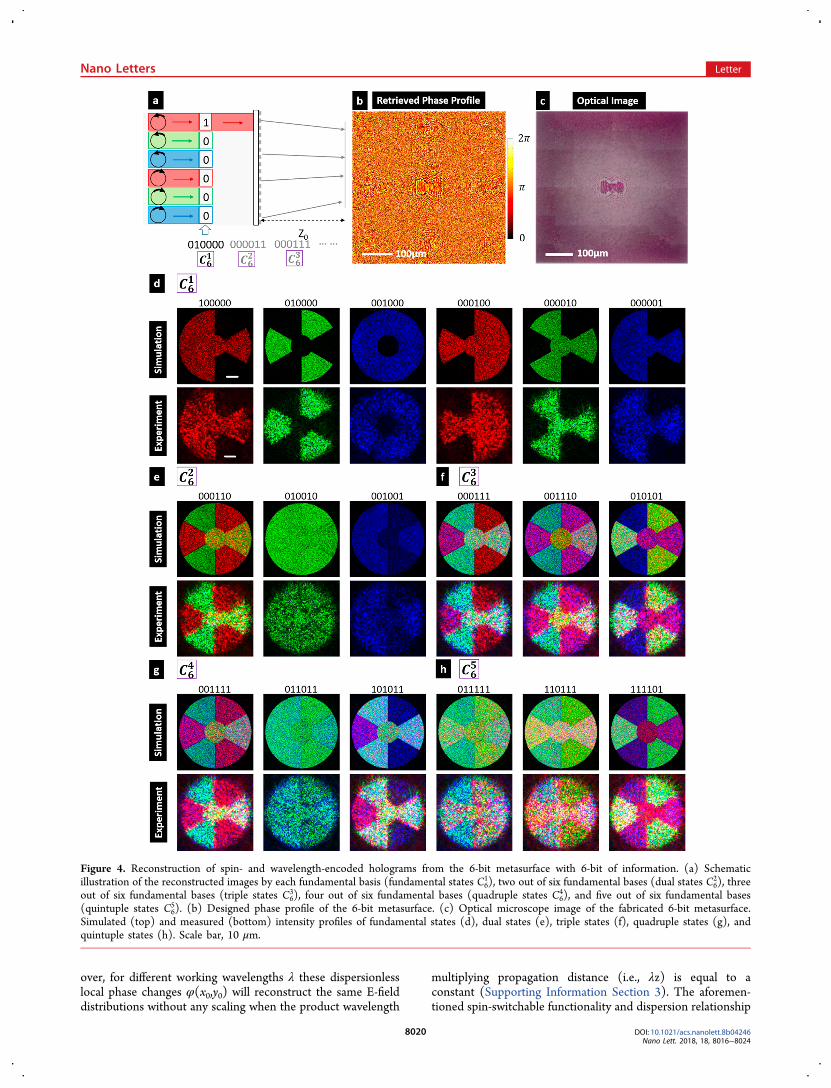
Figure 4. Reconstruction of spin- and wavelength-encoded holograms from the 6-bit metasurface with 6-bit of information. (a) Schematicillustration of the reconstructed images by each fundamental basis (fundamental states C6
1), two out of six fundamental bases (dual states C62), three
out of six fundamental bases (triple states C63), four out of six fundamental bases (quadruple states C6
4), and five out of six fundamental bases(quintuple states C6
5). (b) Designed phase profile of the 6-bit metasurface. (c) Optical microscope image of the fabricated 6-bit metasurface.Simulated (top) and measured (bottom) intensity profiles of fundamental states (d), dual states (e), triple states (f), quadruple states (g), andquintuple states (h). Scale bar, 10 μm.
Nano Letters Letter
DOI: 10.1021/acs.nanolett.8b04246Nano Lett. 2018, 18, 8016−8024
8020

will be used to design wavelength- and spin-dependent meta-hologram.As shown in Figure 2, to realize the wavelength- and spin-
dependent meta-hologram, the key idea is to design and mergetwo-phase profiles, which are operating with the opposite spinsof the three different monochromatic beams to reconstructthree independent images on the same plane, respectively.First, the MWGS algorithm (see detailed description inSupporting Information Section 4) is used to optimize eachphase profile, which can be used to reconstruct three differentindependent images at the given z-plane for the threemonochromatic beams (red, green, and blue). On the basisof the MWGS algorithm, we retrieve two phase profiles,φRCP(x0,y0) (Figure 2a) and φLCP(x0,y0) (Figure 2b), whichrespectively operates for three monochromatic beams withopposite spins to reconstruct three independent images at thesame z-plane (details are shown in Supporting InformationS e c t i o n 5 ) . S e c o n d , t h e f u n c t i o n
e e eA i x y i x y i x y( , ) ( , ) ( , )0 0 RCP 0 0 LCP 0 0= +φ φ φ is used to merge these twophase profiles together, where the angle of this function is themerged phase profile. The final phase profile φ(x0,y0) isencoded onto the metasurface, where the nth phase pixel φn ofthe hologram is represented by a nanobrick with theorientation angle φn/2 as defined in the metasurface. As aresult, (as shown in Figure, 2c) the six independent images onthe same position are switchable, depending on the spins andwavelengths of the incident light. The three differentmonochromatic incident lights with spins can be representedas six fundamental bases (RRCP, GRCP, BRCP, RLCP, GLCP, andBLCP). Therefore, by arbitrarily combining the six fundamentalbases of the input lights, the 6-bit metasurface with (26-1) spin-wavelength-encoded holograms can be realized.Figure 3a presents the calculated phase profile for wave-
length- and spin-dependent meta-hologram. In this design, atotal of 722 500 nanobricks were fabricated occupying a totalarea of 297.5 × 297.5 μm2. Figure 3b shows the opticalmicroscope image of the fabricated Si metasurface. Theschematic diagram of the experimental setup for the holo-graphic reconstruction is shown in Supporting InformationSection 6. The designed meta-hologram reconstructs the “R”,“G”, and “B” letters or the “flower”, “leaf”, and “snowflake”patterns at exactly the same Z position (Z0 = 213.4 μm) fordifferent incident wavelengths by switching the circularpolarization state of the incident beam. As shown in Figure3c, R, G, and B letters are reconstructed by red, green, and bluelasers with RCP (RRCP ,GRCP, and BRCP), while flower, leaf, andsnowflake patterns are reconstructed by red, green, and bluelasers with LCP (RLCP ,GLCP, and BLCP). R, G, B, flower, leaf,and snowflake patterns correspond to the six fundamentalbases, which are encoded by “100000”, “010000”, “001000”,“000100”, “000010”, and “000001”, respectively. Experimentalresults in Figure 3d restore the features of the designed imagesnicely with the image details. According to the image-switchable functionality, the cross-talks induced by oppositespins is switched to Z0 = −213.4 μm. On the basis of thedispersion relationship, the similar holographic imagesreconstructed at different wavelengths are located in differentZ planes (shown in Figures S6 and S7). Because the separationbetween these planes (over 14 μm) is larger than the depth offocus (DOF) of the objective used in this work (DOF is 0.91μm), the cross-talk among different channels is eliminated at
the captured plane of the charge-coupled device (CCD)camera.The 6-bit metasurface with the massive information on (26-
1) bits encoded in color holograms has been realized. Here, wechoose a “ball” pattern as a target image, which is separated tosix different images for six fundamental bases. All images areparts of the ball pattern and are reconstructed in the sameplane. By arbitrarily combining the 6 fundamental bases of theinput beams, the designed 6-bit metasurface can reconstruct 63different spin- and wavelength-dependent holographic images(as shown in Figure 4a). Figure 4b,c presents the calculatedphase profile and optical microscope image of the fabricated 6-bit metasurface, respectively. To characterize the 6-bitmetasurface we modified the experiment setup as shown inSupporting Information Section 7. Compared to the previoussetup (shown in Supporting Information Section 6), abroadband QWP is used and the circular polarization analyzerbefore the CCD camera is removed, which introducesadditional noise to the holographic projections.Figure 4d demonstrates the simulated and measured results
of the reconstructed images of the fundamental states. Asexpected, the holograms generate images with the identical sizeand position for the given wavelength. By selecting thefundamental bases, the fundamental states of the reconstructedimages can be switched. Thanks to the identical position of thereconstructed images, the designed 6-bit metasurface canprovide the compound states of the reconstructed images bycontrolling the combination of the six fundamental bases of theinput light. By choosing two out of three monochromaticincident beams with circular polarizations, the dual statesenable not only the primary colors (RGB) but also theirsecondary colors (cyan, magenta and yellow), as shown inFigure, 4e. When one monochromatic beam with a linearpolarization (i.e., RCP + LCP) illuminates the designed 6-bitmetasurface, the reconstructed image ball with primary colors(i.e., RGB) can be achieved at the observation plane. Inaddition, Figure 4f presents a part of the intensity profiles ofthe triple states. When the metasurface is illuminated by threebeams with different wavelengths and spins simultaneously, thecorresponding triple state shows a full-color (including white)reconstructed image at the observation plane.The designed metasurface also could support quadruple
states and quintuple states, which are shown in Figure 4g,h,respectively. By arbitrarily combining the 6 fundamental basesof the input light, massive information on 63 spin- andwavelength-dependent holographic images can be achieved asshown in Supporting Information Section 8. The measuredintensity profiles of each state show great fidelity with thecolors, shapes, and sizes of the simulated intensity profiles. The6-bit digital code of each intensity profile can be distinguishedby employing correlation functions (Supporting InformationSection 9), and the information on incident beam canconsequently be uniquely determined from the code.The diffraction efficiency is a critical issue related to the
multitasked meta-holograms with massive information. Weprovide a comparison between our noninterleaved method andspatial multiplexed method (Supporting Information Section10) concerning the diffraction efficiency. The diffractionefficiency is defined as the ratio between the power of thereconstructed monochromatic image and the power of theconverted transmitted light.51 Here, the reconstructed imagesof different bits are located at the different areas in the sameplane. Figure S12 shows the average diffraction efficiency of
Nano Letters Letter
DOI: 10.1021/acs.nanolett.8b04246Nano Lett. 2018, 18, 8016−8024
8021

spatial multiplexed method decreases according to 1/N2,41
where N is the number of bit. Compared with spatialmultiplexed method, the higher average diffraction efficienciesof noninterleaved method are achieved, because noninter-leaved method is based on harmonic response.41 Moreover, ifthe reconstructed images move to the same area, non-interleaved metasurface will control the composite wavefrontnear the optical axis without separation, which is able to furtherimprove the energy utilization.In this work, the designed multitasked metasurface is used to
control six fundamental bases of incidences. To estimate thecapacity of a multitasked noninterleaved metasurface, addi-tional fundamental bases of beams at different wavelengths areinvolved in the metasuraface design and the signal-to-noiseratio (SNR) is used to evaluate the quality of reconstructedimages (Supporting Information Section 10). The SNR isdefined by the ratio the between the peak intensity in thereconstructed image and the standard deviation of thebackground noise.51 Figure S13 shows that as the number ofbit increases to 14, even though the average SNR reduces toabout 40, the reconstructions by each fundamental bases arestill recognizable. This introduction of additional fundamentalbases will remarkably increase the information states carried bya single metasurface.In summary, we present a unique approach for achieving the
6-bit metasurface capable of encoding (26-1) color hologramsbased on an array of noninterleaved amorphous Si nanobricks.These massive reconstructed holograms are arisen fromsuperposition and permutation of six fundamental independentimages. This approach not only overcome the cross-talklimitation by single size elements for on-axis illumination butalso realizes a high-capability metasurface with great imagequality. It provides a way for future practical devices withmultiwavelength functionalities that may lead to advances in awide range of fields such as color display, informationencryption, and beam characterization.Sample Fabrication. The sample was fabricated by a
conventional electron beam lithography (EBL). Amorphoussilicon thin films were deposited on fused silica substrates byusing chemical vapor deposition (Oxford PECVD). Thesamples were then spin coated a layer of hydrogensilsesquioxane (HSQ, Dow Corning(R) XR-1541-006) and acharge-dissipation layer (Espacer 300Z) for EBL(Elionix ELS-7000) patterning (acceleration voltage of 100 keV, e-beamcurrent of 200 pA, and exposure dose of 12 mC cm−252). Afterthe exposure, the samples were first rinsed in DI water toremove the Espacer and then developed in the salty developersolution52 for 1 min, followed by DI water, acetone/IPArinsing, and blow dry. The samples were finally etched byreactive-ion-etching in inductively coupled plasma system(Oxford Plasmalab 100) with the following recipe: Cl2 witha flow rate of 22 sccm, ICP power of 400 W, RIE power of 100W, and temperature of 6 °C.Numerical Simulations. Lumerical FDTD Solution (a
commercial software) was used to simulate and optimize theelements of the metasurface. In this simulation, periodicboundary conditions were employed along x- and y-directions,while perfect matched layer was used along z-direction. Thecircular polarized light is formed by two sources polarizedalong x-and y-axes with a phase shift of ±90°, and the circularlypolarized beam is normally incident onto the nanobricks fromthe substrate side. Experimentally measured refraction index ofamorphous Si is used in the simulations (Supporting
Information Section 1). The multipole decomposition iscalculated by the Cartesian multipole analysis based on theelectric field within the Si nanobricks.17,53,54
■ ASSOCIATED CONTENT*S Supporting InformationThe Supporting Information is available free of charge on theACS Publications website at DOI: 10.1021/acs.nano-lett.8b04246.
Material properties used for the simulation, PB phaseintroduced by nanobrick, dispersion relationship, multi-wavelength Gerchberg-Saxton algorithm, detailed illus-tration of phase profiles, experimental setup forcharacterization of the spin and wavelength multiplexedSi hologram, experimental setup for characterization ofthe 6-bit metasurface, reconstruction of 63 spin- andwavelength-dependent holographic images from the 6-bit metasurface, pattern recognition, diffraction effi-ciency and signal-to-noise ratio (PDF)
■ AUTHOR INFORMATIONCorresponding Authors*(C.-W.Q.) E-mail: [email protected]. Telephone: +6565162559.*(J.K.W.Y.) E-mail: [email protected]. Telephone: +6564994767.ORCIDZhaogang Dong: 0000-0002-0929-7723Xiangping Li: 0000-0003-0955-2613Arseniy I. Kuznetsov: 0000-0002-7622-8939Yuri S. Kivshar: 0000-0002-3410-812XJoel K. W. Yang: 0000-0003-3301-1040Cheng-Wei Qiu: 0000-0002-6605-500XAuthor ContributionsL.J. and Z.D. contributed equally to this work. L.J., Z.D., S.M.,J.K.W.Y. and C.W.Q. conceived the idea. L.J. and C.W.Q.designed the hologram nanostructures and did the opticalcharacterization of the hologram. Z.D. and J.K.W.Y did thenanofabrication of the silicon nanostructures. Y.F.Y. did thegrowth of amorphous silicon by using PECVD method. Z.W.provides the expertise knowledge on the Gerchberg-Saxtonalgorithm and pattern recognition. Z.D. and Z.P. did the dryetching of silicon by using the inductively coupled plasma.S.D.R. did the multipole decomposition. X.L., A.I.K. and Y.K.participated in the discussions and contributed with valuablesuggestions for silicon metasurface holograms. The paper wasdrafted by L.J. with inputs from Z.D., J.K.W.Y. and C.W.Q. Allauthors analyzed the data, read and corrected the manuscriptbefore the manuscript submission. C.W.Q. and J.K.W.Y.supervised the project.NotesThe authors declare no competing financial interest.
■ ACKNOWLEDGMENTSC.-W.Q. acknowledges the financial support from the NationalResearch Foundation, Prime Minister’s Office, Singaporeunder its Competitive Research Program (CRP award NRF-CRP15-2015-03). Z.D., Y.F.Y., Z.P., A.I.K., and J.K.W.Y. wouldlike to acknowledge the funding support from Agency forScience, Technology and Research (A*STAR) SERC Pharosproject (Grant 1527300025). In addition, Z.D. and J.K.W.Y.
Nano Letters Letter
DOI: 10.1021/acs.nanolett.8b04246Nano Lett. 2018, 18, 8016−8024
8022

also acknowledge the funding support from A*STAR YoungInvestigatorship (Grant 0926030138), SERC (Grant092154099), National Research Foundation Grant AwardNo. NRF-CRP001-021, NRF-CRP 8-2011-07, and A*STAR-JCO under project number 1437C00135. X.L. acknowledgesNational Natural Science Foundation of China (NSFC)(Grant 61522504) and Guangdong Provincial Innovationand Entrepreneurship Project (Grant 2016ZT06D081).
■ ABBREVIATIONS
PB phase, Pancharatnam-Berry phase; MWGS, algorithmmulti-wavelength Gerchberg-Saxton algorithm; ED, electricdipole; MD, magnetic dipole; RCP, right-circularly polarized;LCP, left-circularly polarized SNR signal-to-noise ratio.
■ REFERENCES(1) Yu, N.; Genevet, P.; Kats, M. A.; Aieta, F.; Tetienne, J. P.;Capasso, F.; Gaburro, Z. Science 2011, 334, 333−337.(2) Yu, N.; Capasso, F. Nat. Mater. 2014, 13, 139−150.(3) Kildishev, A. V.; Boltasseva, A.; Shalaev, V. M. Science 2013, 339,1232009.(4) Levy, U.; Abashin, M.; Ikeda, K.; Krishnamoorthy, A.;Cunningham, J.; Fainman, Y. Phys. Rev. Lett. 2007, 98, 243901.(5) Zhu, A. Y.; Kuznetsov, A. I.; Luk’yanchuk, B.; Engheta, N.;Genevet, P. Nanophotonics 2017, 6, 452.(6) Kristensen, A.; Yang, J. K.; Bozhevolnyi, S. I.; Link, S.;Nordlander, P.; Halas, N. J.; Mortensen, N. A. Nat. Rev. Mater. 2017,2, 16088.(7) Zheng, G.; Muhlenbernd, H.; Kenney, M.; Li, G.; Zentgraf, T.;Zhang, S. Nat. Nanotechnol. 2015, 10, 308−312.(8) Wu, P. C.; Tsai, W. Y.; Chen, W. T.; Huang, Y. W.; Chen, T. Y.;Chen, J. W.; Liao, C. Y.; Chu, C. H.; Sun, G.; Tsai, D. P. Nano Lett.2017, 17, 445−452.(9) Gu, Y.; Zhang, L.; Yang, J. K.; Yeo, S. P.; Qiu, C. W. Nanoscale2015, 7, 6409−6419.(10) Zhou, Z.; Li, J.; Su, R.; Yao, B.; Fang, H.; Li, K.; Zhou, L.; Liu,J.; Stellinga, D.; Reardon, C. P.; Krauss, T. F.; Wang, X. ACS Photonics2017, 4, 544−551.(11) Paniagua-Dominguez, R.; Yu, Y. F.; Khaidarov, E.; Choi, S.;Leong, V.; Bakker, R. M.; Liang, X.; Fu, Y. H.; Valuckas, V.; Krivitsky,L. A.; Kuznetsov, A. I. Nano Lett. 2018, 18, 2124−2132.(12) Huang, K.; Liu, H.; Garcia-Vidal, F. J.; Hong, M.; Luk’yanchuk,B.; Teng, J.; Qiu, C. W. Nat. Commun. 2015, 6, 7059.(13) Zhang, X.; Tian, Z.; Yue, W.; Gu, J.; Zhang, S.; Han, J.; Zhang,W. Adv. Mater. 2013, 25, 4567−4572.(14) Huang, L.; Chen, X.; Muhlenbernd, H.; Li, G.; Bai, B.; Tan, Q.;Jin, G.; Zentgraf, T.; Zhang, S. Nano Lett. 2012, 12, 5750−5755.(15) Paniagua-Domínguez, R.; Yu, Y. F.; Miroshnichenko, A. E.;Krivitsky, L. A.; Fu, Y. H.; Valuckas, V.; Gonzaga, L.; Toh, Y. T.; Kay,A. Y. S.; Luk’yanchuk, B.; Kuznetsov, A. I. Nat. Commun. 2016, 7,10362.(16) Ye, W.; Zeuner, F.; Li, X.; Reineke, B.; He, S.; Qiu, C. W.; Liu,J.; Wang, Y.; Zhang, S.; Zentgraf, T. Nat. Commun. 2016, 7, 11930.(17) Dong, Z.; Ho, J.; Yu, Y. F.; Fu, Y. H.; Paniagua-Dominguez, R.;Wang, S.; Kuznetsov, A. I.; Yang, J. K. Nano Lett. 2017, 17 (12),7620−7628.(18) Karagodsky, V.; Chang-Hasnain, C. Opt. Express 2012, 20 (10),10888−10895.(19) Li, K.; Ran, Y.; Chase, C.; Yang, W.; Chang-Hasnain, C. J.Optica 2018, 5, 10−13.(20) Lalanne, P.; Chavel, P. Laser Photon. Rev. 2017, 11, 1600295.(21) Devlin, R. C.; Ambrosio, A.; Wintz, D.; Oscurato, S. L.; Zhu, A.Y.; Khorasaninejad, M.; Oh, J.; Maddalena, P.; Capasso, F. Opt.Express 2017, 25, 377−393.(22) Wang, L.; Kruk, S.; Tang, H.; Li, T.; Kravchenko, I.; Neshev, D.N.; Kivshar, Y. S. Optica 2016, 3, 1504.
(23) Arbabi, A.; Horie, Y.; Bagheri, M.; Faraon, A. Nat. Nanotechnol.2015, 10, 937−943.(24) Goh, X. M.; Zheng, Y.; Tan, S. J.; Zhang, L.; Kumar, K.; Qiu, C.W.; Yang, J. K. Nat. Commun. 2014, 5, 5361.(25) Kruk, S.; Hopkins, B.; Kravchenko, I. I.; Miroshnichenko, A.;Neshev, D. N.; Kivshar, Y. S. APL Photonics 2016, 1, 030801.(26) Arbabi, E.; Arbabi, A.; Kamali, S. M.; Horie, Y.; Faraon, A. Opt.Express 2016, 24, 18468−18477.(27) Chen, W. T.; Yang, K. Y.; Wang, C. M.; Huang, Y. W.; Sun, G.;Chiang, I. D.; Liao, C. Y.; Hsu, W. L.; Lin, H. T.; Sun, S.; Zhou, L.;Liu, A. Q.; Tsai, D. P. Nano Lett. 2014, 14, 225−230.(28) Khorasaninejad, M.; Chen, W. T.; Zhu, A. Y.; Oh, J.; Devlin, R.C.; Rousso, D.; Capasso, F. Nano Lett. 2016, 16, 4595−4600.(29) Montelongo, Y.; Tenorio-Pearl, J. O.; Milne, W. I.; Wilkinson,T. D. Nano Lett. 2014, 14, 294−298.(30) Zhou, J.; Qian, H.; Hu, G.; Luo, H.; Wen, S.; Liu, Z. ACS Nano2018, 12, 82−88.(31) Balthasar Mueller, J. B.; Rubin, N. A.; Devlin, R. C.; Groever,B.; Capasso, F. Phys. Rev. Lett. 2017, 118, 113901.(32) Levy, U.; Marom, E.; Mendlovic, D. Opt. Lett. 2001, 26 (15),1149−1151.(33) Huang, K.; Dong, Z.; Mei, S.; Zhang, L.; Liu, Y.; Liu, H.; Zhu,H.; Teng, J.; Luk’yanchuk, B.; Yang, J. K.; Qiu, C. W. Laser PhotonicsRev. 2016, 10, 500−509.(34) Huang, L.; Muhlenbernd, H.; Li, X.; Song, X.; Bai, B.; Wang, Y.;Zentgraf, T. Adv. Mater. 2015, 27, 6444−6449.(35) Li, X.; Chen, L.; Li, Y.; Zhang, X.; Pu, M.; Zhao, Z.; Ma, X.;Wang, Y.; Hong, M.; Luo, X. Sci. Adv. 2016, 2, No. e1601102.(36) Avayu, O.; Almeida, E.; Prior, Y.; Ellenbogen, T. Nat. Commun.2017, 8, 14992.(37) Zijlstra, P.; Chon, J. W. M.; Gu, M. Nature 2009, 459, 410−413.(38) Mei, S.; Mehmood, M. Q.; Hussain, S.; Huang, K.; Ling, X.;Siew, S. Y.; Liu, H.; Teng, J.; Danner, A.; Qiu, C. W. Adv. Funct.Mater. 2016, 26, 5255.(39) Mehmood, M. Q.; Mei, S.; Hussain, S.; Huang, K.; Siew, S. Y.;Zhang, L.; Zhang, T.; Ling, X.; Liu, H.; Teng, J.; Danner, A.; Zhang,S.; Qiu, C.-W. Adv. Mater. 2016, 28, 2533.(40) Maguid, E.; Yulevich, I.; Yannai, M.; Kleiner, V.; Brongersma,M. L.; Hasman, E. Light: Sci. Appl. 2017, 6, No. e17027.(41) Maguid, E.; Yulevich, I.; Veksler, D.; Kleiner, V.; Brongersma,M. L.; Hasman, E. Science 2016, 352, 1202.(42) Zhang, C.; Yue, F.; Wen, D.; Chen, M.; Zhang, Z.; Wang, W.;Chen, X. ACS Photonics 2017, 4, 1906−1912.(43) Huang, Y. W.; Chen, W. T.; Tsai, W. Y.; Wu, P. C.; Wang, C.M.; Sun, G.; Tsai, D. P. Nano Lett. 2015, 15, 3122−3127.(44) Wang, B.; Dong, F.; Li, Q. T.; Yang, D.; Sun, C.; Chen, J.; Song,Z.; Xu, L.; Chu, W.; Xiao, Y. F.; Gong, Q.; Li, Y. Nano Lett. 2016, 16,5235−5240.(45) Zhao, W.; Liu, B.; Jiang, H.; Song, J.; Pei, Y.; Jiang, Y. Opt. Lett.2016, 41, 147−150.(46) Li, K.; Guo, Y.; Pu, M.; Li, X.; Ma, X.; Zhao, Z.; Luo, X. Opt.Express 2017, 25, 21419.(47) Deng, Z. L.; Deng, J.; Zhuang, X.; Wang, S.; Li, K.; Wang, Y.;Chi, Y.; Ye, X.; Xu, J.; Wang, G. P.; Zhao, R.; Wang, X.; Cao, Y.;Cheng, X.; Li, G.; Li, X. Nano Lett. 2018, 18, 2885−2892.(48) Wang, K.; Titchener, J. G.; Kruk, S. S.; Xu, L.; Chung, H. P.;Parry, M.; Kravchenko, I. I.; Chen, Y. H.; Solntsev, A. S.; Kivshar, Y.S.; Neshev, D. N.; Sukhorukov, A. A. Science 2018, 361, 1104−1108.(49) Dong, F.; Feng, H.; Xu, L.; Wang, B.; Song, Z.; Zhang, X.; Li, L.Y. X.; Sun, L. F.; Li, Y.; Chu, W. arXiv 2018, 1805.11246.(50) Shi, Z.; Khorasaninejad, M.; Huang, Y. W.; Roques-Carmes, C.;Zhu, A. Y.; Chen, W. T.; Sanjeev, V.; Ding, Z. W.; Tamagnone, M.;Chaudhary, K.; Devlin, R. C.; Qiu, C. W.; Capasso, F. Nano Lett.2018, 18 (4), 2420−2427.(51) Ni, X.; Kildishev, A. V.; Shalaev, V. M. Nat. Commun. 2013, 4,2807.
Nano Letters Letter
DOI: 10.1021/acs.nanolett.8b04246Nano Lett. 2018, 18, 8016−8024
8023

(52) Dong, Z.; Asbahi, M.; Lin, J.; Zhu, D.; Wang, Y. M.;Hippalgaonkar, K.; Chu, H. S.; Goh, W. P.; Wang, F.; Huang, Z.;Yang, J. K. Nano Lett. 2015, 15, 5976−5981.(53) Evlyukhin, A. B.; Reinhardt, C.; Evlyukhin, E.; Chichkov, B. N.J. Opt. Soc. Am. B 2013, 30, 2589−2598.(54) Yang, Y.; Miroshnichenko, A. E.; Kostinski, S. V.; Odit, M.;Kapitanova, P.; Qiu, M.; Kivshar, Y. S. Phys. Rev. B: Condens. MatterMater. Phys. 2017, 95, 165426.
Nano Letters Letter
DOI: 10.1021/acs.nanolett.8b04246Nano Lett. 2018, 18, 8016−8024
8024