non-contractual image · mtm-b8i0120f12ixig_i mtm-b8i0120f12ixig mt series preliminary technical...
TRANSCRIPT

MTM-B8I0120F12IXIG_i
MTM-B8I0120F12IXIGMT Series
PRELIMINARY TECHNICAL INFORMATION
ABOUT MTM SERIES
RECTIFICADORES GUASCH S.A. offers a compact and ready-to-use B8I converter power stack for motorcontrol, inverter applications or active filters. This power stack includes the IGBTs (1/2B2I modules) with aforced-air heatsink and optocoupled drivers. The customer can work in a short delivery time with a widerange of power assemblies in a very compact size.
The MTM series takes the medium range of power from our MT Series of IGBTs power stacks. MT series issuitable to realize converters, choppers, half, full or three phase bridge inverters for motor control, welding,renewable energies, UPS, etc.
Reserves the right to change limits, test conditions anddimensions given in this data sheet at any time without previous
notice.
1
HIGHLIGHTS
- B8I topology- Very compact design- IGBT drivers included- DC-Link capacitor bank included- Ready to use
non-contractual image
BRIEFINGTopology Capacitor bank + B8I
Market Industrial / Educational
Cooling system Extruded heatsink with axial fan array
Driver system SCiCoreDrive22
Max Voltage applied to DClink 800 V
Output current per phase 40 Afsw=10 kHz, TJ<150ºC Tenv=40ºC
fO=50 Hz, PF=0.85, m=1, VDCLINK =600 VDC
user controlinterface
ABC
VDC +
DRIVER SYSTEMGALVANIC ISOLATION
VDC -
D
COM
T1
T2
T3
T4 T6
T5 T7
T8
161
116
Re
v.:0
MTM-B8I0120F12IXIG_i
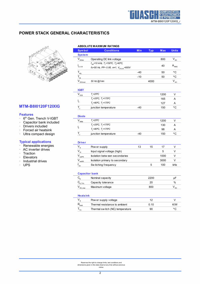
POWER STACK GENERAL CHARACTERISTICS
MTM-B8I0120F12IXIG
Reserves the right to change limits, test conditions anddimensions given in this data sheet at any time without previous
notice.
2
ABSOLUTE MAXIMUM RATINGS
Sym bol Conditions Min Typ Max Units
System
Operating DC link voltage 800
40
-40 50 ºC
-10 50 ºC
50 Hz @1min 4000
IGBT
1200 V
165 A
127 A
junction temperature -40 150 ºC
Diode
1200 V
130 A
98 A
junction temperature -40 150 ºC
Driver
Pow er supply 13 15 17 V
Input signal voltage (high) 5 V
Isolation betw een secondaries 1000 V
Isolation primary to secondary 3000 V
Sw itching frequency 5 100 kHz
Capacitor bank
Nominal capacity 2200
Capacity tolerance 20 %
Maximum voltage 800
Heatsink
Pow er supply voltage 12 V
Thermal resistance to ambient 0.10 K/W
Thermal sw itch (NC) temperature 90 ºC
VDClink
VDC
IU,V,W
fSW
=10 kHz, TJ<150ºC, T
A=40ºC,
ARMSfo=50 Hz, PF= 0.85, m=1, V
DCLink=600V
Tstg
Top
VISOmod
VAC
VCES
TJ=25ºC
IC
TC=25ºC, T
J=175ºC
TC=80ºC, T
J=175ºC
TJ
VRRM
TJ=25ºC
IF
TC=25ºC, T
J=175ºC
TC=80ºC, T
J=175ºC
TJ
VS
ViH
VisolPS
VisolSS
fsw
CN µF
CN_TOL
VDC_max
VDC
VS
RthHA
TTH
Features· 6th Gen. Trench V-IGBT· Capacitor bank included· Drivers included· Forced air heatsink· Ultra compact design
Typical applications· Renewable energies· AC inverter drives· Traction· Elevators· Industrial drives· UPS
MTM-B8I0120F12IXIG_i
POWER MODULE CHARACTERISTICS
Reserves the right to change limits, test conditions anddimensions given in this data sheet at any time without
previous notice.
3
Table 1: IGBT part static characteristics.
IGBT STATIC CHARACTERISTICS
Symbol Parameter Test Conditions Min Typ Max Units
C-E Breakdown Voltage 1200 - - V
C-E Cut-Off Current 3.81 5.08 150G-E Leakage Current 2.17 8.75 200 nA
G-E Threshold Voltage 5.70 6.08 6.45 V
Collector to Emitter 1.75 1.76 1.88 VSaturation Voltage 2.23 2.27 2.40 V
VCES
Tj = 25 °C
ICES
VCE
= VCES
, VGE
= 0 V, Tj = 25 °C µA
IGES
VGE
= VGES
, VCE
= 0 V
VGE(th)
VGE
= VCE
, IC = 4 mA
VCE(sat)
IC = 100 A, V
GE = 15 V, T
j = 25 °C
IC = 100 A, V
GE = 15 V, T
j = 150 °C
Table 2: IGBT part dynamic characteristics.
IGBT DYNAMIC CHARACTERISTICS
Symbol Parameter Test Conditions Min Typ Max Units
Input Capacitance - 9.10 - nF
Output Capacitance - 0.70 - nF
Reverse Transfer Capacitance - 0.80 - nF
Turn-On Delay Time 437 448 495 ns
Rise Time 57.0 59.0 67.0 ns
Turn-Off Delay Time 558 569 630 ns
Fall Time 361 395 465 ns
Turn-On Switching Loss 9.99 10.8 14.0 mJ
Turn-Off Switching Loss 10.8 11.5 15.0 mJ
Total Switching Loss 20.79 22.3 29.0 mJ
Total Gate Charge - 1040 1117 nC
Gate-Emitter Charge - - - μC
Gate-Collector Charge - - - μC
Cies VCE
= 10 V, VGE
= 0 V
f = 1 Mhz, Tj = 25°C
Coes
Cres
td(on) T
j = 150°C, R
G = 1.0 Ω
VDC
= 600 V, IC = 100 A
VGE
= ±15 V
di/dton
= 3230 A/μs
di/dtoff
= 1330 A/μs
du/dtoff = 9350 V/μs
tr
td(off)
tfEon
Eoff
Ets
Qg
VGE
= -8 V...+15 VQge
Qgc
Table 3: Diode part electrical specifications.
DIODE ELECTRICAL CHARACTERISTICS
Symbol Parameter Test Conditions Min Typ Max Units
Diode Forward Voltage1.76 1.79 1.92
V1.86 1.90 1.98
Peak Reverse Recovery Current 107 111 125 A
Diode Reverse Recovery Charge 14.5 15.5 18.0 μC
Diode Reverse Recovery Energy 5.38 6.04 8.00 mJ
VF
IF = 100 A
VGE
= 0 V
Tj = 25 °C
Tj = 150 °C
IRRM
VDC
= 600 V, IC = 100 A
VGE
= ±15 V
di/dtoff
= 3050 A/μs
Tj = 150 °C
Qrr
Tj = 150 °C
Err
Tj = 150 °C
Table 4: IGBT module thermal characteristics.
IGBT MODULE THERMAL CHARACTERISTICS
Symbol Parameter Test Conditions Min Typ Max Units
Thermal Resistance (IGBT Part) Junction-to-Case - 0.197 0.270 °C/WThermal Resistance (Diode Part) Junction-to-Case - 0.434 0.490 °C/W
Thermal Resistance Case-to-Heatsink, per module - 0.02 0.04 °C/W
Rth(J-C)
Rth(J-C)D
Rth(C-H)
MTM-B8I0120F12IXIG_i
COOLING SYSTEM CHARACTERISTICS
The cooling system is formed by a RG14092 extruded heatsink profile assembled with a standard forced airfan rack module SC-C300V40/12 from Semicode.
Note 1:
The thermal resistance values showed are only standard values measured under the following conditions: using 4 modules of 31x91
mm layout footprint with a constant dissipated power equally distributed between modules. The test was perfomed on a power stack
mounted on upright position with fan rack supplied at its nominal supply voltage.
This given data should be taken only as a reference and at any case should replace measurements under real field and on end
application conditions.
Reserves the right to change limits, test conditions anddimensions given in this data sheet at any time without previous
notice.
4
FAN RACK CONFORMALS
Conformal coating MIL-1-46058, Type UR
Security TUV EN60950-1, UL60950-1
Electromagnetic Compatibility CE EN 61000-6-1:2007, EN 61000-6-3:2007
Table 5: Cooling system technical specifications.
Description Symbol Notes / Test conditions Min Typ Max Units
Heatsink thermal resistance Note 1 0.10 K/W
Profile length L 300 mm
Profile section S 5823
Profile perimeter P 2310 mm
Input supply voltage 11.3 12 13.2
Input supply current 1106 1239 mA
Power consumption 13.27 W
Fan rated speed ±10% 8200 rpm
Air Flow Free air 1.93
Static Air Pressure Free air 88.8 Pa
Noise Level per f an 37.5 dBA
Storage Temperature 65% RH -40 70 ºC
Operating Temperature 65% RH -10 70 ºC
Failure Rate 40ºC / 65% RH 70000 h
Thermal switch temperature NC (normally closed) 85.5 90 94.5 ºC
Thermal switch nominal voltage 50/60 Hz 250
Thermal switch nominal current 10 A
Thermal switch threshold histeresis
Rth HA
mm2
VIN DC
VDC
IIN DC
PN
m3/min
Tstg
Top
VN TH VAC
IN TH
30ºC ±10ºCData at T
a = 25 °C, V
IN = 12 V
DC and rated v alues, unless otherwise indicated

MTM-B8I0120F12IXIG_i
CAPACITOR BANK CHARACTERISTICS
Circuit diagram
Warning note:When charged at nominal voltage and then disconnected from DC power source the capacitor bank will be naturally discharged after aproximately 10 min (VC@10min < 2% x VRATED). If a shorter discharge time is needed an external dischargeresistor must be used.
Ripple current
Data given for capacitors is regarding a withstand rms ripple current at 100 Hz and 85ºC. When the hotspotcapacitor bank is operating at a temperature other than 85ºC, the permissible rms current given at 85ºCshould be multiplied by the factors given below:
Reserves the right to change limits, test conditions anddimensions given in this data sheet at any time without
previous notice.
5
Figure 1: Capacitor bank circuit diagram.
VDC +
VDC -
COM
Table 6: Capacitor bank technical specifications.
Description Sym bol Notes / Test conditions Min Typ Max Units
Total bank nominal capacitance ±20% 2200
Maximum voltage 800 V
Surge voltage per capacitor 440 V
Rated working voltage 600 V
Equivalent series resistance ESR per capacitor, 100 Hz 69
Impedance per capacitor, 100 Hz 0.725 mΩ
Ripple current 8.49 A
Leakage current per capacitor 2.64 mA
Mounting position upright or horizontal
20 %
Operating Temperature -40 85 ºC
Useful life 40000 h
CTOT µF
VDC_MAX
VS
VDC
mΩ
ZC
IR per capacitor, 100 Hz, TA=85ºC
ILEAK
CN tolerance
Top
TA=55ºC, at rated I
R
Data at Ta = 25 °C, V
IN = 600 V
DC and rated v alues, unless otherwise indicated
Table 7: Ripple current multiplying factor vs. hotspot temperature.
40ºC 45ºC 50ºC
Multiplying Factor 2.2 2.1 1.9
TC

MTM-B8I0120F12IXIG_i
Where capacitors are required to operate at frequencies other than 100 Hz, the multiplying factors givenbelow may be used to determine the ripple current capacity at that frequency.
e.g.: For an application where the capacitor bank is operating at a 50ºC and ripple current frequency is about 5 kHz the total multiplying factor should be aproximately of 1.9 x 1.35 = 2.5. In that case the total ripple current withstand on DC-Link for the capacitor bank will be of 2 x 8.49 A x 2.5 = 42.45 A.
STACK MOUNTING CONSIDERATIONS
It is necessary a minimum distance of 100 mm with regard to the envelope. The free air circulation should beguaranteed avoiding external nearby heat sources from the assembly.
The power stack must be mounted in upright or horizontal position and tightened to a plane surface using itsmounting fasteners providing a correct heatsink fin air canalization and heatsink thermal performance inorder to accomplish with rated values specified on this datashet, other mounting positions must be avoided.
For real applications it is important to consider a safety margin with regarding the working current, werecommend a margin of the 20%. For critical cases (24 hours work, repetitive overloads, high ambient temperature...), margins of the 30% to50% are used.
Reserves the right to change limits, test conditions anddimensions given in this data sheet at any time without previous
notice.
6
Table 8: Ripple current multiplying factor vs. frequency.
Frequency [Hz] 100 250 1k to 10k >10k
Multiplying Factor 1.0 1.05 1.20 1.35
Table 9: Spacing example with regards the envelope.
100
100

MTM-B8I0120F12IXIG_i
DRIVERS SPECIFICATIONS AND CHARACTERISTICS
MTM-B8I power stacks uses as a driving circuitry the SCiCoreDrive22 2-channel IGBT driver fromSemicode. This is a general purpose 2-channel driver designed to interface IGBTs up to 1200 V. It includes aVCE monitoring for each IGBT which it protects the devices in case of failure by soft turning OFF the IGBTand providing to the user a galvanically isolated fault signal.
The input signaling are Schmidt-trigger, and admits logic levels of 0-5 V or 0-15 V, the MTM-B8I is configuredby default with a 0-5 V input logic but the user can select the best suited configuration. Please see Table 13and Figure 3 to change logic levels configuration.The input signaling also includes a short pulse supressor to avoid undesired triggering glitches andparasites.
For more details and up to date information of the drivers please download the last released SCiCoreDrive22datasheet here.
TECHNICAL DRIVER SYSTEM SPECIFICATIONS
Reserves the right to change limits, test conditions anddimensions given in this data sheet at any time without
previous notice.
7
Figure 2: Input-output chronogram.
Table 10: IGBT drivers power supply technical specifications.
Sym bol Param eter Test Conditions Min Typ Max Units
Supply voltage 13 15 17 VCurrent consumption (full load) 480 mAStand by consumption (no load) 140 mA
VCC
ICC
QG=0.80 μC, f sw=100 kHz ( 2 chan.)
ISTBY
Table 11: IGBT drivers logic inputs and outputs characteristics.
Sym bol Param eter Test Conditions Min Typ Max Units
IN signal high levelSee LOGIC LEVELS
15 VIN signal low level 0 VFAULT output current 8 mA
VIN_H
ICC
ISTBY
Table 12: IGBT drivers timing characteristics.
Symbol Parameter Test Conditions Min Typ Max Units
High output propagation time 2.4 μs
Low output propagation time 2.6 μs
Desat. Detection to FAULT output delay 1.8 5 μs
Blanking time 2.8 μs
Desat. Detection 10% turn off 0.3 0.5 μs
Desat. Detection to 90% turn off 90% 2 3 μs
Reset to fault 3 7 20 μs
Minimum pulse width for RESET 0.1 μs
Max. Switching frequency 100 kHz
DC Duty cycle for IN_x signals 0 100%
td ON
td OFF
td FAULT
tblank
td DES(10)
td DES(90)
td RES_FAULT
PWRES_min
f sw_max

MTM-B8I0120F12IXIG_i
APPLICATION NOTES REGARDING THE DRIVING SYSTEM
LOGIC LEVELS
The inputs of SCiCoreDrive22 (PWMTOP_x, PWMBOT_x and RESET_x) are TTL compatible see its pinout onTable 15. The FAULT_x outputs are open collector outputs, and require an external pull-up resistor.
In addition, the inputs IN_x are schmitt-trigger and admits 2 different voltage levels depending on whetherthe JP1 & JP2 are plugged or not.
Warning note:We recommend to use the 0-15V levels for a better noise immunity on harsh environments. It is not permitted to use different level configuration on each channel. Both channels must work as 0-15 V or 0-5 V. Using 0-15 V input signal when jumpers JP1 & JP2 are plugged can damage the driver. Using 0-5 V or 0-15 V on input signals when drivers are unpowered can also damage the equipment.
SHORT PULSE SUPPRESION (SPS)
Each Input signal (IN_x) of SCiCoreDrive22 includes a SPS to protect the driver and the IGBT fromundesired short duration glitches. A pulse shorter than 1.4 μs will be eliminated with 100% probability. A pulselonger than 1.8 μs will pass the SPS without suffer any change. A pulse with a duration between 1.4 μs and1.8 μs may pass or not.
Reserves the right to change limits, test conditions anddimensions given in this data sheet at any time without previous
notice.
8
Figure 3: Position detail of voltage level input voltage on SCiCoreDrive22.
JUMPERS JP1 & JP2
Table 13: IGBT drivers logic inputs/outputs configurations.
LOGIC INPUTS/OUTPUTS
Symbol Parameter Test Conditions Min Typ Max Units
RST Input signal high level voltage 2 5 VRST Input signal low level voltage 0 0.8 V
IN Input signal high level voltage 3.7 5 V
IN Input signal low level voltage 0 1.3 V
IN Input signal high level voltage 11 15 V
IN Input signal low level voltage 0 3.9 V
VIN_H_RS RESET signal (active when in low-state)VIN_L_RS
VIN5_H_IN IN_x signal
(JP1 & JP2 plugged)VIN5_L_IN
VIN15_H_IN IN_x signal (JP1 & JP2 unplugged)V
IN15_L_IN
MTM-B8I0120F12IXIG_i
FAILURE MANAGEMENT
The power stage of a typical three phase inverter or full bridge is susceptible to several types of failures,most of which are potentially destructive to the power IGBT. Under any of these fault conditions, the currentthrough the IGBT can increase rapidly, causing excessive power dissipation and heating. The IGBT becomedamaged when the current load approaches the saturation current of the device, and the collector to emittervoltage rises above the saturation voltage level. The drastically increased power dissipation overheats veryquickly the power device and destroys it. To prevent damage to the drive, fault protection must beimplemented to reduce or turn-off the over-currents during a fault condition. SCiCoreDrive22 provides fastlocal fault detection and shutdown.
The fault detection method is to monitor the saturation (collector) voltage of the IGBT and to trigger a localfault shutdown sequence if the collector voltage exceeds a predetermined threshold. A small gate dischargedevice slowly reduces the high short circuit IGBT current to prevent damaging voltage spikes. Before thedissipated energy can reach destructive levels, the IGBT is shut off. During the off state of the IGBT, the faultdetect circuitry is simply disabled to prevent false ’fault’ signals.
During normal operation, voltage at RON_x and ROFF_x is controlled by the signal IN_x, with the IGBTcollector to emitter voltage being monitored through VDESAT. The FAULT output is high and the RESETinput must be held high.
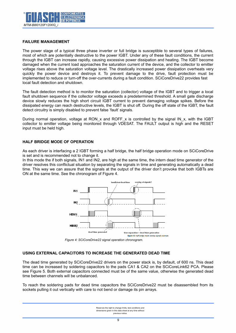
HALF BRIDGE MODE OF OPERATION
As each driver is interfacing a 2 IGBT forming a half bridge, the half bridge operation mode on SCiCoreDriveis set and is recommended not to change it.In this mode the if both signals, IN1 and IN2, are high at the same time, the intern dead time generator of thedriver resolves this conflictual situation by separating the signals in time and generating automatically a deadtime. This way we can assure that the signals at the output of the driver don’t provoke that both IGBTs areON at the same time. See the chronogram of Figure 4.
USING EXTERNAL CAPACITORS TO INCREASE THE GENERATED DEAD TIME
The dead time generated by SCiCoreDrive22 drivers on the power stack is, by default, of 600 ns. This deadtime can be increased by soldering capacitors to the pads CA1 & CA2 on the SCiCoreLink62 PCA. Pleasesee Figure 5. Both external capacitors connected must be of the same value, otherwise the generated deadtime between channels will be unbalanced.
To reach the soldering pads for dead time capacitors the SCiCoreDrive22 must be disassembled from itssockets pulling it out vertically with care to not bend or damage its pin arrays.
Reserves the right to change limits, test conditions anddimensions given in this data sheet at any time without
previous notice.
9
Figure 4: SCiCoreDrive22 signal operation chronogram.

MTM-B8I0120F12IXIG_i
See Table 14 with the relation between the value of the capacitors Cx and the dead time generated.
Warning note:On those applications where one, or more, modules are not in use, e.g.: Three-phase inverter (B6I), the unused module'sdriver must be powered and stuck the both input switching signals to GND to ensure that any spureous signal or noise would not accidentally switch on the IGBT. Never leave any driver unconnected when operating with the power stack.
Reserves the right to change limits, test conditions anddimensions given in this data sheet at any time without previous
notice.
10
Figure 5: Position detail of dead time capacitors pads on SCiCoreLink62.
DM
HB
PWRLED
TOP DEAD TIMECAPACITOR
BOT DEAD TIMECAPACITOR
SCiCoreLink62:
SCiCoreDrive22
SCiCoreLink62
Table 14: Dead time capacitors nominal values.
External capacitor Dead time generated
47 pF 600 ns100 pF 840 ns150 pF 1100 ns220 pF 1350 ns330 pF 1700 ns470 pF 2200 ns680 pF 2900 ns820 pF 4000 ns1000 pF 4600 ns

MTM-B8I0120F12IXIG_i
POWER AND SIGNAL INTERFACES AND CONNECTIONS
DRIVERS I/O INTERFACE AND SUPPLY
Signal connections:
J1 to J4 CONTROL CONNECTORS are the main connectors for each half-bridge driver providing the controlswitching signals for each IGBT, reset signal, and output fault signals. It is also used to supply the drivers+15 VDC. The position of this connectors on the power stack are depicted on Figure 6.
CONNECTOR PINOUT
Connector type:AMP-LATCH series, 5103308-1, TE Connectivity.
Recommeded matched connector socket for PCB-to-PCB connection:AMPMODU series, 5-534206-5, TE Connectivity.
Recommended matched connector socket for PCB to flat cable connection:AMP-LATCH series, 1658621-1, TE Connectivity.
Reserves the right to change limits, test conditions anddimensions given in this data sheet at any time without
previous notice.
11
Figure 6: Position detail of control connectors.
J4 - DRV D
J3 - DRV C
J1 - DRV A
J2 - DRV B
Figure 7: Connector numeration detail.
PIN #10 PIN #1
Table 15: IGBT drivers pinout.
Pin Designator Description
1 Input logic signal for switching TOP IGBT
2 GND Ground terminal for supply and logic signals
3 GND Ground terminal for supply and logic signals
4 RESET Reset input signal (low state)
5 GND Ground terminal for supply and logic signals
6 VCC
7 FAULT Fault output signal
8 VCC
9 VCC
10 Input logic signal for switching BOT IGBT
PWMTOP
+15 VDC
supply voltage
+15 VDC supply voltage
+15 VDC supply voltage
PWMBOT
MTM-B8I0120F12IXIG_i
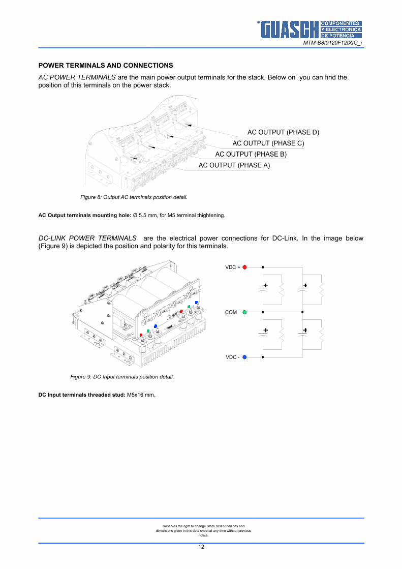
POWER TERMINALS AND CONNECTIONS
AC POWER TERMINALS are the main power output terminals for the stack. Below on you can find the position of this terminals on the power stack.
AC Output terminals mounting hole: Ø 5.5 mm, for M5 terminal thightening.
DC-LINK POWER TERMINALS are the electrical power connections for DC-Link. In the image below(Figure 9) is depicted the position and polarity for this terminals.
DC Input terminals threaded stud: M5x16 mm.
Reserves the right to change limits, test conditions anddimensions given in this data sheet at any time without previous
notice.
12
Figure 8: Output AC terminals position detail.
AC OUTPUT (PHASE D)
AC OUTPUT (PHASE C)
AC OUTPUT (PHASE B)
AC OUTPUT (PHASE A)
Figure 9: DC Input terminals position detail.
VDC +
VDC -
COM

MTM-B8I0120F12IXIG_i
FAN ARRAY SUPPLY AND THERMAL SWITCH SNAP-IN TERMINAL BLOCK
In order to work with the stack user must supply 12 VDC on the snap-in terminal block to power on the fanarray. The equipment should be operated with its fan rack powered on and user must ensure the correctsupply of the fan array.
Please check the power requirements of the fan array and find all thermal switch characteristics stated onTable 5.
Note: Thermal and power performance specifications in this datasheet are given under forced air operation,Rectificadores Guasch do not recommend to use it without power on the fan array or without it. In this case user mustapply a current derating based on custom own power and thermal measurements.
Reserves the right to change limits, test conditions anddimensions given in this data sheet at any time without
previous notice.
13
Figure 10: Snap-in terminal block position detail.
TERMINAL BLOCK
Table 16: Snap-in terminal block pinout.
Pole Designator Description
1 -V GND supply voltage2 +V3 T1 Thermal switch 1
4 T2 Thermal switch 2
+12 VDC
supply voltage
MTM-B8I0120F12IXIG_i
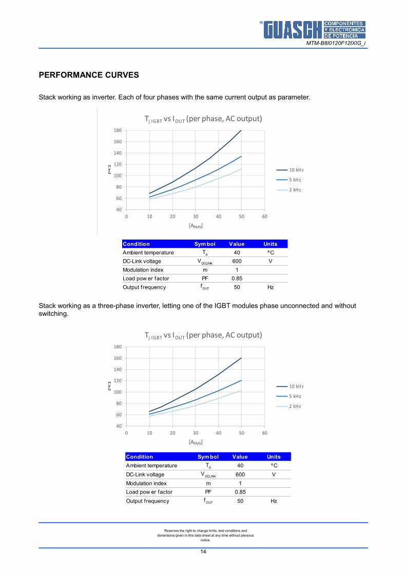
PERFORMANCE CURVES
Stack working as inverter. Each of four phases with the same current output as parameter.
Stack working as a three-phase inverter, letting one of the IGBT modules phase unconnected and without switching.
Reserves the right to change limits, test conditions anddimensions given in this data sheet at any time without previous
notice.
14
40
60
80
100
120
140
160
180
0 10 20 30 40 50 60
[ºC]
[ARMS]
Tj IGBT vs IOUT (per phase, AC output)
10 kHz
5 kHz
2 kHz
Condition Sym bol Value Units
Ambient temperature 40 ºC
DC-Link voltage 600 V
Modulation index m 1
Load pow er factor PF 0.85
Output f requency 50 Hz
TA
VDCLINK
fOUT
40
60
80
100
120
140
160
180
0 10 20 30 40 50 60
[ºC]
[ARMS]
Tj IGBT vs IOUT (per phase, AC output)
10 kHz
5 kHz
2 kHz
Condition Sym bol Value Units
Ambient temperature 40 ºC
DC-Link voltage 600 V
Modulation index m 1
Load pow er factor PF 0.85
Output f requency 50 Hz
TA
VDCLINK
fOUT
MTM-B8I0120F12IXIG_i
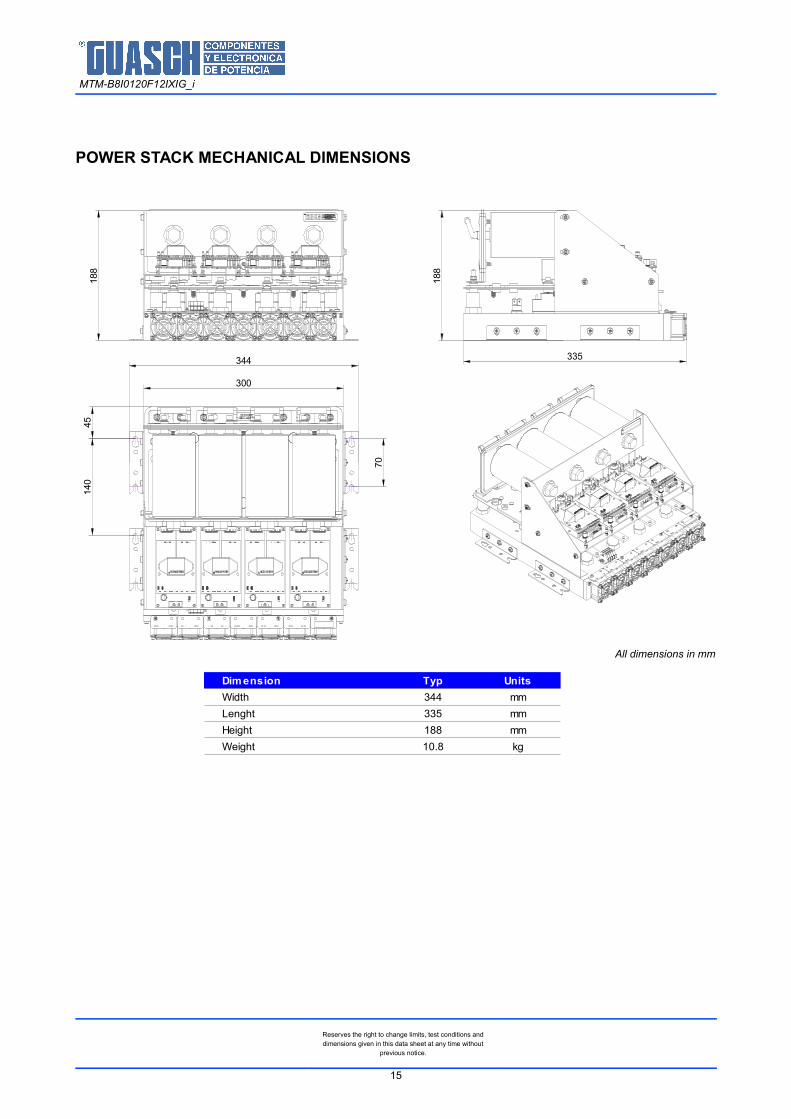
POWER STACK MECHANICAL DIMENSIONS
All dimensions in mm
Reserves the right to change limits, test conditions anddimensions given in this data sheet at any time without
previous notice.
15
188
335
188
344
300
4514
0
70
Dim ension Typ Units
Width 344 mm
Lenght 335 mm
Height 188 mm
Weight 10.8 kg
MTM-B8I0120F12IXIG_i
ANOTACIONES EN LA HOJA DE ESPECIFICACIONES:RECTIFICADORES GUASCH, S.A. utiliza la siguiente anotación para identificar el estado del producto, en el lado izquierdo de laprimera página:
PRELIMINARY TECHNICAL INFORMATION: El producto se encuentra en proceso de diseño y desarrollo. La información presenta losdatos del producto pero algunas características pueden cambiar.ADVANCED TECHNICAL INFORMATION: El producto se encuentra totalmente diseñado y las características se refieren a lafabricación en serie.Sin anotación: Los parámetros del producto están fijados y se suministra de acuerdo con las especificaciones publicadas.
Los datos indicados en esta publicación corresponden a especificaciones de producto, queda exlcuida cualquier garantía expresa o implícita sobre sus propiedades o su aplicación,así como cualquier responsabilidad sobre daños directos o indirectos producidos por los materiales o resultantes de su aplicación. La empresa se reserva el derecho de realizarcambios en las especificaciones de los productos sin previo aviso. La información respecto a métodos de uso y aplicaciones se indica sólo como guía y no constituye garantíaalguna de funcionamiento satisfactorio en un determinado equipo o aplicación. Es responsabilidad del usuario determinar la idoneidad del producto para su aplicación utilizando lainformación disponible y asegurarse de que la misma esta actualizada. Cualquier nombre de producto o marca usada en esta publicación corresponde a marcas depositadas, marcas registradas o nombres protegidos por sus respectivos propietarios.
DATASHEET ANNOTATIONS:RECTIFICADORES GUASCH, S.A. annotate datasheets in the left corner of the front page, to indicate product status:
PRELIMINARY TECHNICAL INFORMATION: The product is in design and development. The datasheet represents the product as it isunderstood but details may change.ADVANCED TECHNICAL INFORMATION: The product design is complete and final characterisation for volume production is well inhand.No Annotation: The product parameters are fixed and the product is available to datasheet specification.
The technical data are to specify components, not to guarantee their properties. No warranty or guarantee expressed or implied is made regarding delivery or performance. TheCompany reserves the right to alter without prior notice the specification of any product. Information concerning possible methods of use is provided as a guide only and does notconstitute any guarantee that such methods of use will be satisfactory in a specific piece of equipment. It is the user’s responsibility to fully determine the performance and suitabilityof any equipment using such information and to ensure that any publication or data used is up to date. All brand names and product names used in this publication are trademarks, registered trademarks or trade names of their respective owners.
© RECTIFICADORES GUASCH, S.A.DOCUMENTACION TECNICA, TECHNICAL DOCUMENTATION
PRODUCIDO EN ESPAÑA, PRODUCED IN SPAINPROHIBIDA SU VENTA, NOT FOR SALE
Your Needs, Our Solutions
Reserves the right to change limits, test conditions anddimensions given in this data sheet at any time without previous
notice.
16