noise margins - ku ittcjstiles/312/handouts/noise margins.pdf · 11/5/2004 noise margins 3/12 jim...
TRANSCRIPT

11/5/2004 Noise Margins 1/12
Jim Stiles The Univ. of Kansas Dept. of EECS
Noise Margins The transfer function of a digital inverter will typically look something like this: Note that there are essentially three regions to this curve:
I. The region where vI is relatively low, so that the output voltage vO is high.
II. The region where vI is relatively high, so that the output voltage vO is low.
III. The transition region, where the input/output voltage is in an indeterminate state (i.e, an ambiguous region between high and low.
vO
vI
V+
V+
1O
I
d vdv
= −
1O
I
d vdv
= −
Transition Region
( )O Iv f v=
I II III

11/5/2004 Noise Margins 2/12
Jim Stiles The Univ. of Kansas Dept. of EECS
Note that the transition region is rather arbitrarily defined by the points on the transfer function where the magnitude of the slope is greater than one (i.e., where 1 0O Id v dv .> ). Although this transfer function looks rather simple, there are actually several parameters that we use to characterize this transfer function—and thus characterize the digital inverter as well! 1. First of all, let’s consider the case when vI=0. The output of the digital inverter in this condition is defined as VOH (i.e., OH “output high”), i.e.:
OHV when 0O Iv v = Thus, VOH is essentially the “ideal” inverter high output, as it is the output voltage when the inverter input is at its ideal low input value vI=0. Typically, VOH is a value just slightly less than supply voltage V+. 2. Now, let’s consider the case when vI =V+. The output of the digital inverter in this condition is defined as VOL (i.e., OL
“output low”), i.e.:
+OLV when VO Iv v =

11/5/2004 Noise Margins 3/12
Jim Stiles The Univ. of Kansas Dept. of EECS
Thus, VOL is essentially the “ideal” inverter low output, as it is the output voltage when the inverter input is at its ideal high input value vI =V+. Typically, VOL is a value just slightly greater than 0. 3. The “boundary” between region I and the transition region of the transfer function is denoted as VIL (i.e., IL “input low”). Specifically, this is the value of the input voltage that corresponds to the first point on the transfer function where the slope is equal to -1.0 (i.e., where 1 0O Id v dv .= − ). Effectively, the value VIL places an upper bound on an acceptably “low” value of input vI—any vI greater than VIL is not considered to be a “low” input value. I.E.:
vO
vI
V+
( )O Iv f v=
VOH
VOL 0

11/5/2004 Noise Margins 4/12
Jim Stiles The Univ. of Kansas Dept. of EECS
IL considered "low" only if VI Iv v <
4. Likewise, the “boundary” between region II and the transition region of the transfer function is denoted as VIH (i.e., IH “input high”). Specifically, this is the value of the input voltage that corresponds to the second point on the transfer function where the slope is equal to -1.0 (i.e., where
1 0O Id v dv .= − ). Effectively, the value VIH places a lower bound on an acceptably “high” value of input vI—any vI lower than VIH is not considered to be a “high” input value. I.E.:
IH considered "high" only if VI Iv v >
vO
vI
V+
V+
1O
I
d vdv
= −
1O
I
d vdv
= −
Transition Region
( )O Iv f v= I II III
VIL VIH

11/5/2004 Noise Margins 5/12
Jim Stiles The Univ. of Kansas Dept. of EECS
Note then that the input voltages of the transition region (i.e., IL IHV VIv< < ) are ambiguous values—we cannot classify them as either a digital “low” value or a digital “high” value. Accordingly, the output voltages in the transition region are both significantly less that VOH and significantly larger then VOL. Thus, the output voltages that occur in the transition region are likewise ambiguous (cannot be assigned a logical state). Lesson learned Stay away from the transition region! In other words, we must ensure that an input voltage representing a logical “low” value is significantly lower than VIL, and an input voltage representing a logical “high” value is significantly higher than VIH. A: Actually, staying out of the transition region is sometimes more difficult than you might first imagine! The reason for this is that in a digital system, the devices are connected together—the input of one device is the output of the other, and vice versa.
Q: Seems simple enough! Why don’t we end this exceedingly dull handout and move on to something more interesting!?

11/5/2004 Noise Margins 6/12
Jim Stiles The Univ. of Kansas Dept. of EECS
For example: Say that the input to the first digital inverter is 1Iv V += . The output of that inverter is therefore 1 OLVOv = . Thus, the input to the second inverter is likewise equal to VOL (i.e.,
2 2 OLVI Ov v= = ).
V+
vI1
V+
vO2 vO1 =vI2
V+
vI1 =V+
V+
vO2 vO1 =vI2 =VOL
Q: So? This doesn’t seem to be a problem—after all, isn’t VOL much lower than VIL??

11/5/2004 Noise Margins 7/12
Jim Stiles The Univ. of Kansas Dept. of EECS
A: True enough! The input vI2=VOL is typically well below the maximum acceptable value VIL. In fact, we have a specific name for the difference between VIL and VOL—we call this value Noise Margin (NM):
L IL OLNM V V Volts= − ⎡ ⎤⎣ ⎦
The noise margin essentially tells us how close we are to the ambiguous transition region for a typical case where I OLv V= . Of course, we do not wish to be close to this transition region at all, so ideally this noise margin is very large! Now, consider the alternate case where vI1 =0.0 V. The output of the first inverter is therefore 1 OHVOv = . Thus, the input to the second inverter is likewise equal to VOH (i.e.,
2 2 OHVI Ov v= = ). V+
vI1 =0.0
V+
vO2 vO1 =vI2 =VOH
Q: This still doesn’t seem to be a problem—after all, isn’t VOH much larger than VIH??

11/5/2004 Noise Margins 8/12
Jim Stiles The Univ. of Kansas Dept. of EECS
A: Again, this is true enough! The input vI2=VOH is typically well above the minimum acceptable value VIH. We can again specify the difference between VIH and VOH as a noise margin (NM):
H OH IHNM V V Volts= − ⎡ ⎤⎣ ⎦
This noise margin essentially tells us how close we are to the ambiguous transition region for a typical case where
0 0 VIv .= . Of course, we do not wish to be close to this transition region at all, so ideally this noise margin is very large! A: Ideally yes. However, in our example we have made one important assumption that in fact may not be true! It turns out that in a real digital circuit, vI2 may not be equal to vO1 !!
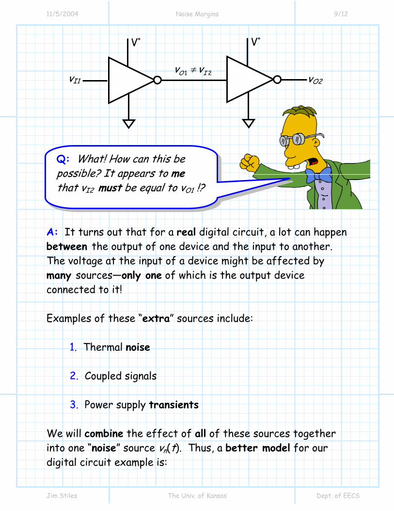
Q: I don’t see why we care about the values of these “noise margins”. Isn’t the simple fact that VOL<VIL and VOH>VIH sufficient?
11/5/2004 Noise Margins 9/12
Jim Stiles The Univ. of Kansas Dept. of EECS
A: It turns out that for a real digital circuit, a lot can happen between the output of one device and the input to another. The voltage at the input of a device might be affected by many sources—only one of which is the output device connected to it! Examples of these “extra” sources include:
1. Thermal noise 2. Coupled signals 3. Power supply transients
We will combine the effect of all of these sources together into one “noise” source vn(t). Thus, a better model for our digital circuit example is:
V+
vI1
V+
vO2 1 2O Iv v≠
Q: What! How can this be possible? It appears to me that vI2 must be equal to vO1 !?

11/5/2004 Noise Margins 10/12
Jim Stiles The Univ. of Kansas Dept. of EECS
Now, let’s reconsider the case where vI1= V+. We find that the input to the second digital inverter is then
( )2 OLVI nv v t= + : Now we see the problem! If the noise voltage is too large, then the input to the second inverter will exceed the maximum low input level of VIL—we will have entered the dreaded transition region!!!! To avoid the transition region, we find that the input to the second inverter must be less than VIL:
V+
vI1
V+
vO2 +
*
vO1
vn(t)
( )2
1
I
O n
vv v t
=
+
V+
vI1 =V+
V+
vO2 +
*
VOL
vn(t)
( )2
OLVI
n
vv t
=
+

11/5/2004 Noise Margins 11/12
Jim Stiles The Univ. of Kansas Dept. of EECS
( )( )( )
OL n IL
n IL OL
n L
V v t Vv t V Vv t NM
+ <
< −
<
Look at what this means! It says to avoid the transition region (i.e., for the input voltage to have an unambiguously “low” digital level), the noise must be less than noise margin NML for all time t! Thus, if the noise margin NML is large, the noise vn(t) can be large without causing any deleterious effect (deleterious effect transition region). Conversely, if the noise margin NML is small, then the noise must be small to avoid ambiguous voltage levels. Lesson learned Large noise margins are very desirable! Considering again the example circuit, only this time with vI=0.0 V, we find that to avoid the transition region (verify this for yourself!):
( )( )( )( )
OH n IH
n IH OH
n H
n H
V v t Vv t V Vv t NMv t NM
+ >
> −
> −
− <
Note that the noise vn(t) is as likely to be positive as negative—it is in fact negative valued noise that will send vI2 to a value less than VIH!

11/5/2004 Noise Margins 12/12
Jim Stiles The Univ. of Kansas Dept. of EECS
Thus, we can make the statement that the magnitude of the noise vn(t) must be less than the noise margins to avoid the ambiguous values of the disturbing transition region! I.E., make sure that:
( ) for all time nv t NM t<