noise and degradation of amorphous silicon devices · noise and degradation of amorphous silicon...
TRANSCRIPT
Noise and degradation ofamorphous silicon devices

Druk: PrintPartners Ipskamp - Enschede

Noise and degradation ofamorphous silicon devices
Ruis en degradatie van amorf silicium structuren
(met een samenvatting in het Nederlands)
PROEFSCHRIFT
TER VERKRIJGING VAN DE GRAAD VAN DOCTOR AAN DE
UNIVERSITEIT UTRECHT OP GEZAG VAN DE RECTOR MAG-NIFICUS, PROF. DR. W.H. GISPEN, INGEVOLGE HET
BESLUIT VAN HET COLLEGE VOOR PROMOTIES IN HET
OPENBAAR TE VERDEDIGEN OP MAANDAG 6 OKTOBER
2003 DES MIDDAGS TE 12.45 UUR
DOOR
JEROEN PIETER ROELOF BAKKER
GEBOREN OP 16 FEBRUARI 1976, TE OSS

PROMOTOR: PROF.DR. J.I. DIJKHUIS
FACULTEIT NATUUR- EN STERRENKUNDE
DEBYE INSTITUUT
UNIVERSITEIT UTRECHT
CIP-GEGEVENS KONINKLIJKE BIBLIOTHEEK, DEN HAAG
BAKKER, JEROEN PIETER ROELOF
NOISE AND DEGRADATION OF AMORPHOUS SILICON DEVICES/JEROEN BAKKER. - UTRECHT: UNIVERSITEIT UTRECHT,FACULTEIT NATUUR- EN STERRENKUNDE, DEBYE INSTITUUT
PROEFSCHRIFT UNIVERSITEIT UTRECHT.MET SAMENVATTING IN HET NEDERLANDS.ISBN 90-393-3303-3TREFW.: HALFGELEIDERS / SILICIUM / AMORF / RUISSPECTROSCOPIE /DEGRADATIE.

Opgedragen aan mijn grootvadersPieter Jacobus Bakker en Roelof Timmerman
Contents
1 Introduction 101.1 Hydrogenated amorphous silicon . . . . . . . . . . . . . . . . . 10
1.1.1 General properties . . . . . . . . . . . . . . . . . . . . . 101.1.2 Electronic properties . . . . . . . . . . . . . . . . . . . . 111.1.3 Degradation of a-Si:H . . . . . . . . . . . . . . . . . . . 14
1.2 Noise spectroscopy . . . . . . . . . . . . . . . . . . . . . . . . . 161.3 Noise measurements on amorphous silicon . . . . . . . . . . . 17
1.3.1 1/f noise in coplanar structures of doped a-Si:H . . . . 181.3.2 1/fα noise in coplanar structures . . . . . . . . . . . . . 191.3.3 1/fα noise in sandwich structures of undoped a-Si:H . 20
1.4 Aim and outline of this thesis . . . . . . . . . . . . . . . . . . . 23
2 Devices, conductivity and setup 252.1 Devices . . . . . . . . . . . . . . . . . . . . . . . . . . . . . . . . 25
2.1.1 Positioning of the device in the setup . . . . . . . . . . 252.1.2 Contact requirements . . . . . . . . . . . . . . . . . . . 252.1.3 Device structure . . . . . . . . . . . . . . . . . . . . . . 262.1.4 Device preparation . . . . . . . . . . . . . . . . . . . . . 262.1.5 Device properties . . . . . . . . . . . . . . . . . . . . . . 28
2.2 Device simulations . . . . . . . . . . . . . . . . . . . . . . . . . 292.2.1 Simulation program . . . . . . . . . . . . . . . . . . . . 292.2.2 Simulation of J-V curves . . . . . . . . . . . . . . . . . 302.2.3 Band bending . . . . . . . . . . . . . . . . . . . . . . . . 322.2.4 Uniform resistivity layer . . . . . . . . . . . . . . . . . . 33
2.3 Setup . . . . . . . . . . . . . . . . . . . . . . . . . . . . . . . . . 35
3 Study of g-r noise 373.1 Introduction . . . . . . . . . . . . . . . . . . . . . . . . . . . . . 37
6

CONTENTS 7
3.2 Ingredients of g-r noise theory . . . . . . . . . . . . . . . . . . . 393.2.1 Relaxation . . . . . . . . . . . . . . . . . . . . . . . . . . 403.2.2 Multi-level model . . . . . . . . . . . . . . . . . . . . . . 413.2.3 Green’s function procedure . . . . . . . . . . . . . . . . 43
3.3 Calculation of g-r noise intensity . . . . . . . . . . . . . . . . . 453.3.1 Computational details . . . . . . . . . . . . . . . . . . . 453.3.2 Rates and spectra . . . . . . . . . . . . . . . . . . . . . . 47
3.4 Discussion of the model assumptions . . . . . . . . . . . . . . 523.5 Conclusion and perspectives . . . . . . . . . . . . . . . . . . . 54
4 Long-range potential fluctuations 554.1 Introduction . . . . . . . . . . . . . . . . . . . . . . . . . . . . . 554.2 Theory . . . . . . . . . . . . . . . . . . . . . . . . . . . . . . . . 58
4.2.1 Autocorrelation function . . . . . . . . . . . . . . . . . . 584.2.2 Single layer approach . . . . . . . . . . . . . . . . . . . 594.2.3 Screening . . . . . . . . . . . . . . . . . . . . . . . . . . 614.2.4 Description of deep defects . . . . . . . . . . . . . . . . 644.2.5 Activation barriers . . . . . . . . . . . . . . . . . . . . . 674.2.6 Rates and rate equations . . . . . . . . . . . . . . . . . . 684.2.7 From potential fluctuations to noise . . . . . . . . . . . 70
4.3 Temperature dependence . . . . . . . . . . . . . . . . . . . . . 734.3.1 Noise spectra . . . . . . . . . . . . . . . . . . . . . . . . 734.3.2 Distribution of potential barriers . . . . . . . . . . . . . 754.3.3 Dutta-Dimon-Horn analysis . . . . . . . . . . . . . . . . 764.3.4 Discussion of Dutta-Dimon-Horn analysis . . . . . . . 78
4.4 General discussion . . . . . . . . . . . . . . . . . . . . . . . . . 784.5 Conclusion . . . . . . . . . . . . . . . . . . . . . . . . . . . . . . 804.6 Appendix: Equilibrium statistical description . . . . . . . . . . 81
5 Further experimental evidence 835.1 Introduction . . . . . . . . . . . . . . . . . . . . . . . . . . . . . 835.2 Devices . . . . . . . . . . . . . . . . . . . . . . . . . . . . . . . . 855.3 Experimental results . . . . . . . . . . . . . . . . . . . . . . . . 865.4 Conclusion . . . . . . . . . . . . . . . . . . . . . . . . . . . . . . 90
6 Noise study of degradation 916.1 Motivation . . . . . . . . . . . . . . . . . . . . . . . . . . . . . . 916.2 Measurements on silver-epoxy contacted devices . . . . . . . . 92
6.2.1 Measurement conditions . . . . . . . . . . . . . . . . . . 92

8 CONTENTS
6.2.2 Effect of degradation . . . . . . . . . . . . . . . . . . . . 926.3 Analysis of noise data of silver-epoxy contacted devices . . . . 93
6.3.1 Parallel resistances . . . . . . . . . . . . . . . . . . . . . 936.3.2 Extraction of the degradation term in the noise . . . . . 946.3.3 Noise data of degraded part . . . . . . . . . . . . . . . . 95
6.4 Measurements in wire-bonded devices . . . . . . . . . . . . . . 956.4.1 Measurement conditions . . . . . . . . . . . . . . . . . . 966.4.2 Device simulations . . . . . . . . . . . . . . . . . . . . . 976.4.3 SCLC analysis . . . . . . . . . . . . . . . . . . . . . . . . 996.4.4 Noise measurements in wire-bonded devices . . . . . . 99
6.5 Conclusion . . . . . . . . . . . . . . . . . . . . . . . . . . . . . . 100
7 Diffusion noise in TFTs 1037.1 Introduction . . . . . . . . . . . . . . . . . . . . . . . . . . . . . 103
7.1.1 Thin-film transistors . . . . . . . . . . . . . . . . . . . . 1037.1.2 1/f noise in the on-state of TFTs . . . . . . . . . . . . . 1047.1.3 Aim . . . . . . . . . . . . . . . . . . . . . . . . . . . . . . 105
7.2 TFT characterization . . . . . . . . . . . . . . . . . . . . . . . . 1057.2.1 TFT fabrication . . . . . . . . . . . . . . . . . . . . . . . 1057.2.2 Linear transfer characteristics . . . . . . . . . . . . . . . 106
7.3 Noise measurements . . . . . . . . . . . . . . . . . . . . . . . . 1087.3.1 Noise in the above-threshold regime . . . . . . . . . . . 1087.3.2 Noise spectra in the sub-threshold regime . . . . . . . . 108
7.4 1D Diffusion noise . . . . . . . . . . . . . . . . . . . . . . . . . 1097.4.1 1D diffusion noise theory . . . . . . . . . . . . . . . . . 1097.4.2 Fits to the spectral kink . . . . . . . . . . . . . . . . . . 1107.4.3 Mobility from noise intensity . . . . . . . . . . . . . . . 1117.4.4 Total number N from noise intensity . . . . . . . . . . . 1127.4.5 Mobility and N directly computed from the conduc-
tion only . . . . . . . . . . . . . . . . . . . . . . . . . . . 1147.5 Discussion . . . . . . . . . . . . . . . . . . . . . . . . . . . . . . 115
7.5.1 Diffusion noise phenomenon . . . . . . . . . . . . . . . 1157.5.2 Mobility values . . . . . . . . . . . . . . . . . . . . . . . 115
7.6 Conclusion and outlook . . . . . . . . . . . . . . . . . . . . . . 116
References 117
Summary 123

CONTENTS 9
Samenvatting voor niet-vakgenoten 127
Dankwoord 131
Curriculum Vitae 135

Chapter 1
Introduction
1.1 Hydrogenated amorphous silicon
1.1.1 General properties
The crystalline form of the material silicon is well known for numerous ap-plications in information technology. The material is used to make struc-tures with a specific purpose, devices. The manufacturing of silicon de-vices relies very much on the advantagous properties of oxides and nitrides,which are insulators, allowing for the fabrication of structures with alternat-ing semiconductor-insulator layers. In that way, charge carriers can be effec-tively confined and/or controlled. The addition of various concentrations ofdopant atoms yields silicon layers with the desired electron concentration.Various combinations of doped, intrinsic, insulator and contact layers haslead to a multitude of devices. A few examples of crystalline silicon (c-Si)devices are the transistor, the optical sensor, and the solar cell.Two types of devices play a role in this work: the solar cell and the thinfilm transistor. A solar cell consists at least of layers of p-type doped and n-type doped material, and sometimes of intrinsic material in between. Lightgenerates mobile electrons and holes, which are separated by an internalelectric field and collected at the contacts. In the field-effect-transistor (FET)a variable electric field at the semiconductor/insulator interface is used tocontrol the concentration of charge carriers in a conducting channel near theinterface. The current through the conducting channel can even be switchedon and off by application of a properly chosen electric field.The invention of the disordered variant of crystalline silicon (c-Si), amor-phous silicon (a-Si) provided a perspective to reduce material costs of solar
10

1.1 HYDROGENATED AMORPHOUS SILICON 11
cells, since it can be deposited as thin layers, on large area’s while c-Si solarcells require wafers, which are relatively thick and expensive. Whereas c-Sihas an indirect bandgap, a-Si can be considered as a direct semiconductor.Further, the amorphous structure exhibits a significant variation of bond an-gles between the atoms, which turns out to lead to dangling bonds with alarge defect density in the band gap, which enhances electron-hole recom-bination, and limits the conductivity of the material. However, defects canbe passivated to a large extent when hydrogen is incorporated in the amor-phous network during growth.Hydrogenated amorphous silicon (a-Si:H) can be formed by dissociation of amixture of silane (SiH4) and hydrogen (H2) in a plasma deposition process.The concentration of deep defects in a-Si:H is reduced by the presence of hy-drogen, but still orders of magnitude higher than in c-Si. Trapping of chargecarriers by the deep defects in a-Si:H limits the efficiency of solar cells andthe mobility of thin film transistors (TFTs). The doped layers which are nec-essary in these devices are created by addition of phosphorus- and boron-containing gases. For a review of a-Si:H see Ref. [1].
1.1.2 Electronic properties
The randomness of the amorphous network leads to the presence of elec-tronic states below the conduction band, which are localized. These statescan capture electrons and are called tail states, which refers to the exponen-tial tail representing their distribution in energy. Optical absorption mea-surements allow for sensing the density of states profile, which rapidly de-creases below the conduction band. In a logarithmic representation of thedensity of states in Fig. 1.1, the exponential distributions of tail states nearthe band edges are straight lines. According to Mott, the transition betweenlocalized states and extended states is sharp and marks the energy abovewhich electrons are mobile [2]. In view of that, the conduction band edgeEC is often called the mobility edge. However, the properties of states nearthe mobility edge are actually more complicated (see Ref. [1]). The theoryof conductivity near the mobility edge in disordered systems has been de-bated for many years and is still not completely agreed on. Nevertheless,for practical purposes, the conduction of a-Si:H films can well be describedin terms of the mobility edge. The conduction appears to be thermally acti-vated with a barrier EC −µ, in case electrons are the majority carriers. Here,µ is the chemical potential, which is defined as the average energy requiredto add a single electron to the system. It is the widespread practice to refer

12 INTRODUCTION
ECE
V
p(E)
p' E')(
Density
ofsta
tes
(logscale
)
Energy
FIGURE 1.1: Schematic presentation of the density of states in the centerof the band gap, including extended states below the valenceband edge EV and above the conduction band edge EC , tailstates within the band gap, and two Gaussian distributions ofdefect states. p(E) is related to transitions involving a singleelectron and p′(E′) involves a second electron, shifted by thecorrelation energy U , i.e. E′ = E + U .

1.1 HYDROGENATED AMORPHOUS SILICON 13
to the chemical potential of a semiconductor as ”the Fermi level”, althoughthere is a subtle difference [3]. The Fermi level namely is the energy levelwhere the electron occupation is one-half. The Fermi level coincides withµ at zero temperature. Also at higher temperatures, where the distributionof electrons is spread thermally, the Fermi level is shifted and effectivelycoincides with µ. Given the continuous distribution of levels in the gap ofan amorphous semiconductor, the Fermi level effectively tracks an existinglevel where the occupation number equals one-half. In the context of amor-phous semiconductors ”Fermi level” and ”chemical potential” are thus syn-omyms. We choose to use the term ”chemical potential” in this thesis. Incase of crystalline semiconductors, which have no or very few discrete (im-purity) levels in the band gap, the difference between the two terms is morepronounced, since the Fermi level in general does not coincide with an ex-isting level in the gap. Therefore the term ”chemical potential” is preferredin case of crystalline semiconductors [3].In intrinsic (undoped) a-Si:H the chemical potential is located in the midgapregion. Dangling silicon bonds constitute the deep defects, which are closeto midgap and may contain up to two electrons. The dangling bonds canbe singly occupied (D0), doubly occupied (D−) or empty (D+). To put asecond electron on a singly occupied defect requires an extra energy U , thecorrelation energy. All existing defect models assume a Gaussian energydistribution of deep defects. The simplest defect model uses two Gaussiandistributions; one of these is related to transitions to and from the doublyoccupied defect states and is therefore shifted in energy by U (see Fig. 1.1).Above the conduction band edge the density of states deviates from thesquare-root dependence on the energy in crystalline materials [1].An important phenomenon observed in some disordered structures is perco-lation. Due to the random position of the atoms in the network, the potentiallandscape depends strongly on the local configuration of the atoms. Elec-trons, when injected in the structure, tend to follow a current path throughthe lower (localized) energy states. At a specific energy, the percolationthreshold, excitation over the saddle points of the potential landscape is pos-sible and various parts of the film get connected, resulting in a conductiveflow. A percolation description, however, turns out not to fully describe thephysics around the mobility edge of a-Si:H.The existence of a random distribution of charged deep defects in undopeda-Si:H results in long-range potential fluctuations of the conduction and va-lence band edges. The amplitude and spatial frequencies of the potentialfluctuations are different for undoped, doped and compensated amorphous

14 INTRODUCTION
silicon.The electronic properties of hydrogenated amorphous silicon are usuallystudied below the annealing temperature (∼ 420 K), where the amorphousstructure is ’frozen in’. At temperatures below 200 K variable-range hop-ping in tail states limits the conduction of this material [4]. In the cases ofa-Si and silicon suboxides, which have defect densities larger than the typi-cal defect density of a-Si:H , variable-range hopping is observed up to roomtemperature [5].
1.1.3 Degradation of a-Si:H
A serious drawback for commercial application of a-Si:H in devices is degra-dation of the electronic properties over time due to defect creation. In case ofsolar-cell devices, prolonged exposure to light leads to breaking of weak Si-Si bonds via electron-hole recombination. As a concequence, newly createddefects can lead to either rotation or breaking of Si-H bonds. In a degradedsolar cell the defect density is thus increased, which enhances total recom-bination and reduces the efficiency. Degradation in a-Si:H is a reversible pro-cess and called the Staebler-Wronski effect [6]. By thermal annealing thematerial can reach a state equivalent to the original state.In case of thin-film transistors (TFTs), where electrons are injected in thechannel region of a transistor due to a high applied voltage at the gate con-tact, trapping is enhanced, Si dangling bonds are created, which leads toa shift of the threshold voltage. The threshold voltage corresponds to thegate voltage, at which all deep defects are filled. Gate stressing createsa higher defect density and a threshold-voltage shift. It is believed that thedefect-creation reactions in solar cells and TFTs have a common origin [7].A large number of experimental studies on defect creation kinetics of a-Si:H resulted in an empirical law: the defect density depends sub- linearlyon both the illumination time and power and saturates after a sufficientlylong period of illumination. Branz formulated microscopic kinetic equa-tions with a corresponding exact solution [8]. Deane et al. have introducedthe thermalization energy concept for defect creation, and measured the ac-tivation energy and attempt-to-escape frequency of this process [9]. Com-pared to defect creation, thermal annealing has a much higher energy bar-rier and a higher attempt-to-escape frequency [10]. That suggests that defectcreation and annealing are caused by a different mechanism. Progress in thedescription of defect creation kinetics has been made by recognizing that thereverse reaction by thermal annealing is not negligible at finite temperature

1.1 HYDROGENATED AMORPHOUS SILICON 15
(see Refs. [10, 11]).More than ten microscopic models have been proposed for the microscopicmechanism that would explain the Staebler-Wronski effect [7] and still, thereare ongoing discussions in literature about the microscopic description ofdefects and the degradation mechanism. An important issue is the distancetraveled by hydrogen atoms after defect creation. Electron spin resonance(ESR) measurements are instrumental in discriminating between the mod-els. When hydrogen atoms would remain at the bond- centered position,the separation between the dangling bond and hydrogen atom would beabout 0.2 nm, which would lead to a measurable hyperfine broadening ofthe ESR signal, but which has never been observed [12]. This experimentalfact seems to favor mechanisms involving long-range hydrogen motion. Inthe hydrogen collision model, mobile H travels through the network until it“collides” with another mobile H, thus accounting in a natural way for thewide separation between the dangling bond and hydrogen as indicated byESR experiments. As mentioned before, Branz’ model also explains the ob-served defect creation kinetics [8].Recently, Powell et al. proposed a solution for the inconsistency of their lo-cal defect-pool model [13] with ESR data. They suggested that the hydrogenatom is located in the tetrahedral-like site instead of the bond centered site inthe amorphous network [7]. The microscopic mechanism for defect creationproposed by Powell et al. is as follows [7]: light or gate bias (in case of TFTs)causes accumulation of electron- hole pairs and electrons, respectively, onshort, weak Si-Si bonds, which then break due to released energy from re-combinations. A hydrogen atom from another, neighboring weak Si-Si bondthen moves to the tetrahedral-like site of the broken Si-Si bond. The improveddefect-pool model takes the chemical equilibrium description of the defects inthe three different charge states (+,0,-) into account [13]. The related hydro-gen density of states is described in Ref. [14]. Defect formation leads to anenergy shift of the peak of formed defects, consistent with a minimum freeenergy. In other words, the ratios between the three kinds of newly createddefects depend on the location of the chemical potential. In doped layers,the chemical potential is located close to the band edge, resulting in a sur-plus of defect states at energies near the opposite band edge. Without thedefect-pool model that observation would have remained a mystery.

16 INTRODUCTION
1.2 Noise spectroscopy
The main experimental technique used in this thesis is electrical noise spec-troscopy, which turns out to complement standard conductivity measure-ments. Electrical noise measurements analyze the amplitude and the spe-cific time constants of spontaneous electrical fluctuations. The coherence ofa noise signal V (t) is revealed by transforming it into the frequency domain.Experimentally, V (t) is measured an its autocorrelation function 〈V (t)V (0)〉computed, which is subsequently Fourier transformed to obtain the noisespectrum SV (f). The mathematical connection is the so-called Wiener-Khin-tchine theorem [15], which reads
SV (f) = 4∫ ∞
0〈V (t)V (0)〉 cos(2πft) dt. (1.1)
Electrical noise can be classified in equilibrium and non-equilibrium noise,corresponding to noise in absence or presence of current. In zero currentconditions, thermal velocity fluctuations of charge carriers lead to thermalnoise, which has a noise level proportional to temperature and film resis-tance. Since the spectra have equal intensity in the full frequency range, itis called ’white noise’ or Johnson-Nyquist noise. Thermal noise is usuallysubtracted from the total noise intensity to study the excess noise.In the presence of current, several types of non-equilibrium noise can exist,either induced by current, or originating from resistance fluctuations. Shotnoise is a fundamental type of noise which corresponds to current fluctua-tions of uncorrelated charged particles, and depends linearly on current. Itleads to a white current noise spectrum and is commonly found in e.g. semi-conductor diodes. Two examples of resistance fluctuations with compara-ble noise spectra are random telegraph signal noise (RTSN) and generation-recombination (g-r) noise. These two classes of noise signals can only bedistinguished because of their different behavior in the time-domain. Incase of RTSN, the device resistance fluctuates as a result of an individualrandom fluctuator which can occupy two different states. The measuredtime-trace of the voltage over the device will show random switching be-tween two levels. The average time the system spends in each of the twostates are denoted τup and τdown, corresponding to the voltage level, whichswitches between up or down. The effective time τeff which appears as acut-off frequency in the noise spectrum is given by [16]
1τeff
=1
τup+
1τdown
. (1.2)

1.3 NOISE MEASUREMENTS ON AMORPHOUS SILICON 17
The effective frequency 1/(2πτeff ) separates two parts of the Lorentzian spec-trum: a part at lower frequencies, which is white, and a part with spectraldependence 1/f2 at higher frequencies.In contrast, the voltage signal of generation-recombination noise is in generaluncorrelated due to the presence of more than two (uncorrelated) levels.Here, the fundamental processes are capture and emission transitions ofcharge carriers between trap and/or band levels [17]. When a fluctuationcauses an excess in the number of majority carriers, the time it takes to re-store that fluctuation, and reach the average number, is characterized by thisexponential relaxation time τ . The relaxation time τ in g-r noise has the samerole in the noise spectrum as the effective time in RTSN. For a process char-acterized by a single relaxation time, the spectrum is Lorentzian. In case ofthermally activated processes and a broad distribution of energy levels thespectrum will be 1/f [18]. However, in many cases Fermi statistics imply anarrow effective distribution of relaxation times, i.e. over a range of ∼ 4kBT[19], and the spectrum is Lorentzian again.Generally, the transport of charge carriers in a semiconductor with traps canbe described by taking generation-recombination, drift, and diffusion intoaccount [17]. In the special case where diffusion is the only relevant term,the spectrum will show different branches with a distinct slope. The devicegeometry determines the occurrence of 1-, 2- or 3-dimensional diffusion noise.Irrespective of geometry, a spectral dependence ∝ 1/f3/2 is observed in thebranch at the highest frequencies.Another noise source which is found in virtually all physical systems is 1/fα
noise, where α is close to unity and may depend on temperature and/orfrequency. When the 1/f noise is inversely proportional to the number ofcarriers, Hooge’s law is satisfied [20]. The analysis is then limited to the de-termination of the empirical, so-called Hooge parameter. Occasionally, thenoise can be attributed to a superposition of Lorentzian noise sources thathave a sufficiently broad range of characteristic time constants [18]. This ap-proach was shown to work for a number of metal-oxide films [18, 21], butthe model inherently fails to predict the absolute noise intensity.
1.3 Noise measurements on amorphous silicon
In the following, low-frequency noise measurements on hydrogenated amor-phous silicon performed up to now are reviewed. The low-frequency rangeof the measurements refers to a typical range from 1 Hz to 10 kHz. The

18 INTRODUCTION
measurements are classified according to the device geometry and doping.Finally, some attention is paid to degradation studies.
1.3.1 1/f noise in coplanar structures of doped a-Si:H
Many contributions to the examination of 1/f noise in amorphous siliconare from Kakalios’ group (University of Minnesota, USA). In a number ofpublications a connection between correlated or non-Gaussian 1/f noiseand long-range disorder was established [22], but recent experiments haveraised some doubt about that interpretation [23, 24], and are discussed laterin this section. Noise measurements in n-type doped a-Si:H devices in copla-nar geometry reveal 1/f noise and ’noise in the noise’ close to 1/f . Themeasured correlation between noise in different parts of the spectrum wasattributed to the spontaneous fluctuations of current filaments which in turnaffect the conduction of neighboring filaments. The choice for a coplanargeometry forces the current through a relatively long path, connecting localminima of the potential landscape. Random resistor lattice simulations pre-dict the presence of current filaments near the percolation threshold [22, 25].The activation energies measured from thermopower and conduction aredifferent [22, 23], which was ascribed to the influence of long-range disor-der on the electronic transport states (see also Ref. [26]).In several studies the material composition was varied or alternatively thematerial was degraded by illumination, and the effect on the noise spectraexamined. Fan and Kakalios measured an increase in the Gaussian behaviorof the 1/f noise upon light soaking of an n-type a-Si:H film [27]. Accord-ing to the authors, that could point to weaker correlation between filamentsin the presence of a higher defect density. In contrast, Quicker, West, andKakalios found no change in the non-Gaussian statistics after degradation oftwo n-type films, a compensated film and a sulfur-doped film [28]. Later,this was confirmed by measurements of Belich and Kakalios on (degraded)n-type devices prepared under various deposition conditions [23]. In ad-dition, those devices exhibited no change in activation energy EQ, whichwas independently determined from thermopower and conduction mea-surements and was proposed as a measure for the long-range potential land-scape.In an ultimate attempt to probe the correlation of the noise a recent experi-ment was performed on an a-Si:H film with ’crystalline’ silicon small parti-cles of ∼ 150 nm in diameter [24]. The size of these particles was so smallthat they contained just one filament on average (the estimated filament-

1.3 NOISE MEASUREMENTS ON AMORPHOUS SILICON 19
diameter was 1 µm). If interactions between filaments would be the pri-mary cause of the noise statistics then one would expect the statistics inthe nano-particles to be Gaussian. Therefore, a mixture of Gaussian andnon-Gaussian components was expected in the film. However, the noisestatistics of coplanar devices with or without nano-particles turned out tobe identical! That, together with the absence of an increase in the Gaussianstatistics after degradation [23, 24], puts the original explanation of Fan andKakalios in serious doubt. Belich and Kakalios conclude that the noise stud-ied in Kakalios’ group might have been not as universal as was previouslyclaimed [23, 24]. Belich and Kakalios suggest that very few noisy filamentsor other fluctuators may dominate the noise and mask contributions from(changes in) the bulk material. That might also explain why the noise in-tensity diverges at the percolation threshold. In a comparable situation foran system with uncorrelated noise, the noise would vanish at zero bias cur-rent. Instead, the observed noise varies from device to device, due to thestrong sensitivity to local filaments. The conclusion applies also to the earlywork of Parman and Kakalios [29], reviewed by Verleg [30], and further toParman’s later work [31].
1.3.2 1/fα noise in coplanar structures
A Canadian research group, consisting of Gunes, Johanson and Kasap, hasstudied noise in undoped and doped thin films of a-Si:H and of a-SiGe:Halloys in coplanar geometry [32, 33, 34, 35, 36]. The films exhibit Gaus-sian statistics, in contrast to the non-Gaussian statistics found in the filmsof Kakalios’ group. In order to reach a sufficiently low film resistance, noisemeasurements were performed mainly in the temperature range 450 K to500 K. Unintensionally, significant structural changes must have been in-duced since the temperature was above the thermal annealing of a-Si:H (420K) [4]. Hydrogen movement plays a crucial role in that process. It is verylikely that mobile hydrogen diffuses through the network at the tempera-tures of the experiment. Even out-diffusion of hydrogen is known to occur[37].The observed 1/f noise exhibits a quadratic dependence on bias current.The noise spectra show two branches each fitting to a 1/fα power law butwith different slopes α and different temperature dependences. In the low-frequency range and for undoped films, α ≈ 1.2. Further, the noise intensityis independent of temperature, but α increases slightly with temperature.In the high-frequency range, α ≈ 0.6 and temperature independent, but the

20 INTRODUCTION
noise intensity decreases rapidly with temperature. Gunes et al. distinguishtwo different noise mechanisms based on the difference in temperature de-pendence of the two branches [32]. However, they do not propose a mi-croscopic mechanism to explain the observations in the two regions. Theirmeasurements were followed by the investigation of the influence of the Gecontent in a-SiGe:H on the noise spectra [35, 36]. Further, in p-type a-Si:Hfilms, the slope parameter α increases with temperature from near unity toover 1.4, for temperatures from 295 K to 473 K [33], while marked deviationsfrom a strict power law are observed. A degradation study of n-type a-Si:Hfilms revealed a decrease of the parameter α from 1.1 to 0.8 upon degra-dation. The exact mechanisms underlying this multitude of effects are notclarified so far.
1.3.3 1/fα noise in sandwich structures of undoped a-Si:H
The first paper on noise measurements on non-hydrogenated undoped a-Sidates back from 1985 [38], was performed in a sandwich configuration, andreports on 1/fα noise with α ≈ 1.16 at room temperature. A second paper,by Baciocchi et al., describes measurements on hydrogenated amorphoussilicon [39]. Both thin films (0.2 - 0.5 µm) were sandwiched between Cr con-tacts. The 1/fα excess noise spectra exhibit a frequency dependent slope α.The noise intensity level and its quadratic dependence on the voltage overthe device points to resistance fluctuations. These features and the spectralshape turn out to be similar to the observations in sandwich structures car-ried out later in our group.The first publication on nin (sometimes denoted n-i-n, referring to electrondoped-intrinsic-electron doped layers) a-Si:H devices with a 2-µm-thick in-trinsic layer and Cr contacts appeared in 1987 from the hands of Bathaei andAnderson [40]. The noise was found to exhibit a 1/fα dependence with 0.7< α < 1.1. The authors explicitly reported an increasing spectral slope withfrequency. The slope in the high-frequency range (∼1 kHz) increases withtemperature. From the temperature dependence of the conductivity and thenoise intensity at 1 kHz, the activation energies were found to be 0.91 eVand 1.10-1.17 eV, respectively.The work of Verleg and Dijkhuis on 1.5-µm-thick 1 nin a-Si:H films con-firmed the frequency dependence of the slope of 1/fα noise spectra: 0.6< α < 1.4 [41, 42], measured in a broader frequency domain, from 1 Hz to
1We re-determined the device thickness using a DekTak step profiler.

1.3 NOISE MEASUREMENTS ON AMORPHOUS SILICON 21
100 kHz. An example of a noise spectrum, measured in comparable con-ditions and reproducing the result of Verleg, is presented in Fig. 1.2. The
100
101
102
103
104
10-15
10-14
10-13
10-12
10-11
Frequency (Hz)
SV
/V
2 (
Hz-1
)
0.6 0.8 1.00.0
1.0x10⁻⁴
2.0x10⁻⁴
3.0x10⁻⁴
Energy (eV)
DA
E (ar
b. u
nit
s)
FIGURE 1.2: Relative voltage noise intensity of a 1-µm-thick nin a-Si:H de-vice, B1, measured at 50-mV bias voltage (in Ohmic condi-tions), at 402 K. The inset shows the effective distribution ofactivation energies (DAE) responsible for the (curvature of)noise spectra at various temperatures, calculated from Dutta-Dimon-Horn analysis [18]. The energy scale was derivedfrom the temperature dependence of the characteristic fre-quency, while the analysis was carried out using data at 10Hz () and at 100 Hz (). For details of device B1, refer toTable 2.1.
measured noise exhibits Gaussian statistics, indicative of uncorrelated noiseand a V 2-dependence on the bias voltage in the Ohmic regime. In addition,the slope at a fixed frequency (10 Hz) was found to decrease with temper-ature. The activation energies of the conduction and the apparent charac-teristic noise frequency were found to be 0.73 eV and 0.83 eV, respectively[41]. The corner frequency f1 in the noise is defined as the frequency wherethe spectral shape is exactly 1/f . What it measures can unfortunately not becompared directly with the temperature dependence of the noise intensityat fixed frequency found by Bathaei and Anderson. Nevertheless, the generalobservation of a larger activation energy of noise compared to conduction islikely to be the clue to the explanation for the noise in sandwich structuresof a-Si:H.The noise spectra could be successfully analyzed using the phenomeno-

22 INTRODUCTION
logical Dutta-Dimon-Horn approach [18, 21], owing to the the thermallyactivated behavior of the noise in sandwich a-Si:H devices [41]. The ap-proach assumes the presence of a distribution of energy barriers, and con-siders thermally activated transitions between various two-level systems.The effective distribution of activation energies D(Ea) takes the occupationnumbers of all energy levels into account. For a proper analysis, D(Ea) isrequired to vary slowly on the scale of kBT . Then, the effective distributionfollows from the noise spectrum, using
SV (ω, T ) ∝ kBT
ωD(Ea), (1.3)
where Ea = −kBT ln(ω/ω0), and ω0 is to be determined from the temper-ature dependence of the characteristic frequency f1. Clearly, an exact 1/fspectrum corresponds to a constant D(Ea). However, in case of a slowlyvarying effective distribution, the resulting noise spectrum will be 1/fα,with α close to unity. Finally, we note that the proportionality sign in Eq.(1.3) indicates that the DDH-approach does not quantitatively predict thenoise intensity level.Verleg and Dijkhuis concluded that the frequency and temperature depen-dence of the voltage noise spectra can be traced back to originate from asingle distribution of the barriers governing the thermally activated pro-cesses [41]. We carried out the analysis on a new device and qualitativelyreproduced the distribution of activation energies (see inset of Fig. 1.2).The original explanation for the observed noise spectra and barrier distribu-tion was given in terms of generation-recombination noise processes takingplace at deep traps. The experimental and analytical work of Reynolds [43]and Main [44] also considers generation-recombination noise as the expla-nation for the observations.Importantly, two other groups have experimentally studied 1/f noise in un-doped nin a-Si:H devices inspired by the publication of Verleg’s work. Re-cent results were reported by Kasap et al., who found a slope parameterα = 0.96 in a sandwich device at T = 375 K. In a small frequency range, theydo not observe a significant change of the spectral slope, despite the signifi-cant degree of band bending in the studied device [45]. The measured noiseintensity, however, is of the same order of magnitude as for our devices.Again, inspired by the work at Utrecht University, Goennenwein et al. com-bined noise spectroscopy and electron paramagnetic resonance (EPR) to studynin a-Si:H devices. For a continuously illuminated device, application ofa magnetic field leads to resonant changes in the electronic noise of semi-

1.4 AIM AND OUTLINE OF THIS THESIS 23
conductors, predominantly at the central time constant 1/f1. That allowsfor the direct identification of a defect state dominating noise under non-equilibrium conditions. Hole hopping in the valence band tail is identifiedas the dominant spin-dependent step governing the noise under illumina-tion conditions, when the number of holes is comparable to the number ofelectrons.
1.4 Aim and outline of this thesis
The aim of this thesis is to obtain a quantitative description of observed1/f noise in a-Si:H films and of noise in a-Si:H thin-film transistors. Wewill show that noise spectroscopy is a new tool to obtain information onthe structural electronic changes in the material. To reach our goals, a thor-ough analysis of the conductivity data is needed and performed in Chapter2, from which all relevant device parameters are deduced. The value forthe device parameters are used as input for a the quantitative analysis of thenoise measurements. Our goal is to predict both the intensity and the shapeof the noise spectrum.In Chapter 3, a quantitative generation-recombination theory for one-dimensional devices is applied to our device using the material- and deviceparameters. The existing theory is extended to a system with a large num-ber of defect states within the band gap. Our research contributes to theunresolved question whether g-r noise can produce 1/f noise.In Chapter 4, a first-principle approach is presented to describe long-rangepotential fluctuations in nin a-Si:H devices. Local fluctuations of theCoulomb potential due to charged defects lead to voltage fluctuations viathe screening by surrounding defects and by the contacts. The theory iscapable to quantitatively predict both the noise intensity and the spectralshape, measured at different temperatures, and provides new insight in thedistribution of barriers above the conduction band edge due to the randomlocation of charged defects. Experimental data obtained from p-type dopedsandwich structures is presented and analyzed in Chapter 5, yielding infor-mation about the potential landscape below the valence band edge. Further,the distribution of barriers from a deuterated film is compared to the resultfrom a hydrogenated film.In Chapter 6 we report on the effect of prolonged illumination on the noiseintensity of a-Si:H. Previous work left us with an apparent contradiction:while a slight increase of the noise intensity is to be expected, an increase

24 INTRODUCTION
by a factor of 10 was observed [30]. A proper analysis turns out to explainthat increase in rather trivial terms. New measurements show only a slightincrease of the noise intensity, which turns out to be consistent with the the-ory presented in Chapter 4.Finally, Chapter 7 deals with thin-film transistors (TFTs), which have the in-teresting feature that the concentration of charge carriers in the conductingchannel is controllable via the gate voltage. The noise measurements arefocused to the near-threshold regime, in which diffusion noise in the one-dimensional conducting channel turns out to dominate. A quantitative anal-ysis of the noise yields the effective diffusion coefficient and the mobility inthe near-threshold regime, consistent with conductivity measurements.

Chapter 2
Devices, conductivity and setup
2.1 Devices
2.1.1 Positioning of the device in the setup
The device holder is located in a vacuum chamber, which is electrically Con-nected to other parts of the setup. The copper holder, which is in thermalcontact with a heater, has room for a removable copper block. The substratewhich is glued on top of the copper block provides good thermal contactbetween the device and the heater. The copper holder contains a Pt100thermocouple, allowing for temperature monitoring and stabilization bya Lakeshore temperature controller between room temperature and 450 K.Our thin-film a-Si:H devices have typical dimensions 7×8 mm and are gluedonto the central gold-square of a special ceramic substrate (of 27 mm2) us-ing a conducting silver epoxy, EPOTEK P1011. A hardening step is requiredof 1 hour, during which the entire substrate is kept at 150 C. A copper oraluminum wire is electrically connected between the top contact and a goldpad on the substrate (see Fig. 2.1).
2.1.2 Contact requirements
Low-ohmic electrical contacts with top- and bottom layers are required forour electrical measurements. To reduce oxidation, we need noble metal ascontact material. Unfortunately, sputter deposition of gold is impossible.We decided to use copper instead, and to insert titanium as a barrier to pre-vent copper ions from diffusing into the material at high temperatures andcausing contamination of the semiconductor. In some cases, a metal oxide
25

26 DEVICES, CONDUCTIVITY AND SETUP
GoldGold
Back
FIGURE 2.1: Ceramic device substrate and its golden contact pads plottedto scale. Back contact pad is indicated. Top-contact of thedevice, is glued on the central pad, and connected to a goldpad via a copper wire or an aluminum bond.
forms between the contact and the semiconductor film, signified by a strong1/f noise and a relatively large device resistance in the high (400 K) temper-ature range, preventing usefull noise measurements.
2.1.3 Device structure
For our noise measurements, we use amorphous silicon devices with a doped-intrinsic-doped sandwich structure, either nin or pip. To avoid direct contactbetween the back metal layers and amorphous silicon layers, we did not usea glass substrate but a low-resistivity (1-3 Ωcm) n++ doped c-Si wafer (seeFig. 2.2). In case of the pip devices a p++ wafer was used, instead. The cur-rent runs through the sandwich structure to the wafer, metal layers, silverepoxy, and the central gold-pad (see Fig. 2.2). The contact materials weresputtered in the same run using a mask, which leaves a square of 5×6 mmuncovered for metal deposition (the lightly shaded part in Fig 2.1). Sputter-ing was performed under UHV conditions in a clean-room environment.The native oxide between the wafer and the amorphous silicon film is roughlyone monolayer thick [46], thin enough to ensure that electrons can tunneleasily through it and do not contribute to the noise. The estimated resis-tance of the 500 µm n++ c-Si wafer is 1 mΩ.
2.1.4 Device preparation
Prior to deposition the wafer was cleaned in a 66% HNO3 solution for 10minutes, followed by a HF dip during 2 minutes, and finally a water dip.

2.1 DEVICES 27
Ag epoxy
30 nm Cu
30 nm Ti
30 nm Cu
50 nm doped a-Si:H
doped a-Si:H50 nm
Au
200 nm Ti
Ceramic substrate
500 µm c-Si wafer(highly doped)
1 µm i-type a-Si:H
FIGURE 2.2: Cross section of the layered device (not to scale). Indicatedthicknesses are standard values, from which actual deposi-tion data might deviate (see Table 2.1).
Hydrogenated amorphous silicon is deposited in the Utrecht Solar EnergyLab. (USEL) on a wafer by dissociation of silane gas (SiH4). All devices re-ported in this study where grown by Plasma Enhanced Chemical Vapor De-position (PECVD). This deposition technique is based on the enhancementof gas dissociation into various radical species by electrons in a plasma. Theapplied RF field was set to a frequency of 13.56 MHz, while the substratetemperature was stabilized at 468 K. Under these conditions the growth rateis 0.20 nm/s. Additional gases can be admitted in the reactor to passivateand to grow doped layers: hydrogen (H2) for passivation, phosphine (PH3)for n-type, and tri-methylborane (TMB) for p-type layers. Application ofa relatively high RF power (10 W instead of 3 W for amorphous n-layers)made the p-type layers microcrystalline, which gives the best possible lay-ers. The energy barrier height between the p-type layer and the metal con-tact is estimated to be as small as 0.06 eV [47], approximately 2kBT at roomtemperature. The intrinsic layer of deuterated amorphous silicon deviceswas deposited using SiD4. Each intrinsic layer was exposed to air beforeand after deposition of the intrinsic layer. Another air exposure was neededprior to sputter deposition of the metal layers. Despite some unavoidableoxidation of the surfaces we could detect no signs of contact noise.The devices used in this thesis are specified in Tab. 2.1. To each batch is

28 DEVICES, CONDUCTIVITY AND SETUP
assigned a character, while numbers indicate different samples of the samebatch. The nin devices were made in batch A, B and batch D, the latter withdeuterium (D) in the intrinsic layer. In batch C pip devices were deposited.For comparisson, the conditions for the nin devices of Verleg are includedas batch V.The procedure for the measurement of the device thickness makes use of
device structure n layer (nm) i layer (µm) area (cm2)A nin 55 1.1 0.55B1 nin 40 0.91 0.55B2 nin 40 0.91 0.64B3 nin 40 0.91 0.11C pip 28 (p) 0.84 0.57D1 nin (D) 55 1.12 0.57D2 nin (D) 55 1.12 0.55D3 nin (D) 55 1.12 0.56V nin 50 1.50 0.56
TABLE 2.1: Area and thickness of the devices.
the fact that the substrate is contained in a strip mask. The strips are thinmetallic ribbons, 1-mm wide, that cover the substrate partially. Depositionof amorphous silicon creates a vertical step along the edges of the mask. Thisstep is indicated in the cross section of the a-Si:H structure shown in Fig 2.2.A Dektak step profiler was used to determine the height of this vertical step,which equals the total thickness of all amorphous silicon layers. Since batchA was deposited without such a step, its thickness was estimated from thegrowth rate and deposition time.
2.1.5 Device properties
In case of batch C, the holes are the majority carriers and the conductivity σequals peµp, with µp the hole mobility. ¿From the measured J-V character-istics in the Ohmic regime, the conductivity prefactor σ0 was determined at(7 ± 1)·103 Ω−1m−1. In case of batch B, the electrons are the majority carriersand the conductivity σ is given by neµn, with µn the electron mobility. Themeasured conductivity prefactor σ0 is found to be a factor of three largercompared to pip a-Si:H devices. The unavoidable difference in thickness be-tween the devices C and B1 has influence on the conductivity prefactor and

2.2 DEVICE SIMULATIONS 29
therefore prevents a direct determination of the ratio µn/µp. Assuming thatNV = NC , we estimate for intrinsic PECVD a-Si:H material grown at 468 Kthat µn ≈ 3µp.The nin device with hydrogen (B1) has a 35-% higher conductivity than thedevice with deuterium (D1), while the deuterium device is 23% thicker, dueto a different growth rate than anticipated. As a result, the dilution withdeuterium during the deposition process might have been larger.
2.2 Device simulations
2.2.1 Simulation program
To analyze time-dependent fluctuations, the steady-state electrical proper-ties have to be known to sufficient precision. Some can be found in liter-ature, others have to be determined from experiments on a device from aspecific batch, since material properties may vary from batch to batch. Forexample, the activation energy of the conduction is determined from themeasured temperature dependence of the J-V characteristics in the linearregime, where J is the current density and V the voltage. The idea devel-oped in this thesis is to use a computer simulation program to extract defectparameters relevant for our noise measurements, by adjusting the parame-ters to the non-linear part of the J-V curve. This procedure is called inversefitting.A variety of computer programs is available to compute the steady-stateelectrical properties in layered semiconductor films by solving the Poissonequation and the continuity equations for electrons and holes. Input param-eters are mobility, defect concentrations, etc. We used the Windows versionof AMPS-1D [48], in which deep defects are modeled using two Gaussiandistributions while the tail states are approximated by exponential distribu-tions. Further details are given below.We checked that other, even more advanced programs, based on the so-called Defect Pool Model [13] produce qualitatively the same band diagramas AMPS-1D. The comparison was made with results obtained from an ex-tended version of AMPS-1D, D-AMPS-1D [49] and ASA [50]. The quanti-tative difference in the results obtained out of these more computer-time-consuming models turned out to be negligible for our purposes.Amphoteric defects deep in the gap play an important role in amorphoussilicon and have the ability of capturing zero, one or two electrons, and con-sequently have three charge states called D+, D0, and D−, respectively. An

30 DEVICES, CONDUCTIVITY AND SETUP
amphoteric defect in the D0 state can either capture or emit an electron.The model description of defects is limited to only two kinds of transitions.Capture corresponds to acceptor levels, and emission to donor levels in thatmodel. A typical donor transition is D− → D0+e. Defect states are assumedto be distributed in energy according to a Gaussian profile. Donor and ac-ceptor states are separated by the correlation energy U . For example, in thetypical acceptor transition D0 + e → D−, the additional energy needed toput a second electron on the defect equals U .The one-dimensional device simulation program AMPS-1D [48] computes aset of electron and hole concentrations and potential as a function of positionthat is consistent with the measured J-V curve for all given combinations oftemperatures, bias voltages, and even illumination intensities. Details ofthe AMPS-program are available on the AMPS-web site (see Ref. [48]) andin Chapter 2 of Van Veghel’s masters thesis [51]. The transitions betweendefect levels and carrier bands are described using the Shockley-Read-Hallmodel (see section 3.2.2).
2.2.2 Simulation of J-V curves
In order to reduce the number of free parameters in our model, we use es-timates from literature. Using the measured activation energy of an n-typelayer of PECVD a-Si:H [52], we find the same activation energy in the calcu-lated band diagram for a donor density of 3.3·1017 cm−3. In order to mimicthe smooth connection between the n-layer and the contact, we fixed thecontact potential φ to 0.20 eV.Capture cross-sections were set to 1·10−15cm2. The tail states were modeledby an exponential energy distribution below the band edges, with a decayfactor of 0.03 eV for the conduction band and 0.045 eV for the valence band,respectively. The electron mobility µn was fixed to 10 cm2V−1s−1 [1].The fitting procedure was performed in two steps in which we adjusted tothe linear and the non-linear part of the J-V curve, respectively. ¿From thefit to the linear part of the J-V curve at three temperatures we obtain: densityof states at the conduction band edge NC(EC) and the band gap. The for-mer is obtained via the temperature-independent prefactor of the conduc-tivity µnNC(EC), and the latter from the activation energy of conductionthat characterizes the interaction between the band gap Eg and the defectlevels, with central positions E0 and E′
0, representing the D+ ↔ D0 transi-tions and the D0 ↔ D− transitions, respectively. With a fixed band gap, wesubsequently fitted to the non-linear part of the J-V curve in order to extract

2.2 DEVICE SIMULATIONS 31
the defect density nD, the central positions of the D+/D0 level E0, and theD0/D− level E′
0 with respect to the valence band edge EV , and the width2∆E of the Gaussian energy distribution of these defect levels. These defectparameters turn out to be important parameters for computing the absolutenoise intensities in our device.The central positions of the Gaussian defect distributions E0 and E′
0 influ-ence the location of the Fermi level, and therefore are adjusted until the tem-perature dependence of the linear part of the data fits well. It turns out thatthe sensitivity of the non-linear part to the width ∆E is rather small. Inour approach, we can determine the above mentioned defect parameters in-cluding nD within 10 % by a fitting procedure which requires only a fewdata points.A typical example of our fit is plotted in Fig. 2.3, and shows the excellentagreement between simulation and experiment. The fitted parameters are
0.01 0.1 110-4
10-3
10-2
10-1
100
101
102 295 K 363 K 417 K fit
Voltage (V)
Cu
rren
t d
ensi
ty
J (
mA
/cm
2)
FIGURE 2.3: J − V characteristics of nin a-Si:H device B1 at three temper-atures, including the result of fitting according to parameterset (1).
listed in Table 2.2. Since the number of fitting parameters is large, some am-biguity of the fitting parameters exists. To indicate the range in the fittedvalues in case of device B1, parameter set (1), parameter set (2), both lead-ing to acceptable fits, are included. For the thin devices of batch B, equallywell fits can be obtained with a defect density that ranges from 4 to 8 ·1015
cm−3, while for the thicker devices that range is narrower. The first lines ofthe table show the two measured (not adjusted) quantities: the activation

32 DEVICES, CONDUCTIVITY AND SETUP
energy of conduction Eσ and the thickness of the intrinsic layer.
Measured parameters A B1 (1) B1 (2)Activation energy Eσ 0.68 eV 0.63 eV 0.63 eVThickness i-layer 1.1 µm 0.91 µm 0.91 µmAdjustable parametersNC(EC) 3.4·1020cm−3 2.0·1020cm−3 3.35·1020cm−3
Defect density nD 2.5·1015 cm−3 6.0·1015 cm−3 4.6·1015 cm−3
Bandgap Eg 1.82 eV 1.80 eV 1.80 eVD+/D0 level E0 − EV 0.78 eV 0.95 eV 0.89 eVD0/D− level E′
0 − EV 1.12 eV 1.15 eV 1.09 eVResulting parametersEC0-µ n.a. 0.63 eV 0.71 eVEB0-EC0 n.a. 0.27 eV 0.19 eV
TABLE 2.2: Device parameters, obtained from direct measurement orfitting with AMPS. Fixed parameters: mobility µn = 10cm2V−1s−1, contact potential φ = 0.20 eV, correlation energyU = 0.20 eV and the halfwidth ∆E of the defect distributions= 0.15 eV. The energy levels EC0 and EB0 indicate the conduc-tion band edge and the average barrier height (see section 4.3),respectively.
2.2.3 Band bending
A typical band diagram (for thin devices) consistent with all J-V measure-ments is plotted in Fig 2.4. The coordinate x is perpendicular to the film.The variable xT is the characteristic length of the uniform resistivity layer,which will be introduced in section 2.2.4. Further, the location and thicknessof the n++-doped layers and the intrinsic layer are indicated. The diagramshows the conduction band profile EC(x) and the chemical potential µ. Zeroenergy is chosen at the valence band edge EV in the doped layers. The dop-ing induces a high electron concentration in the intrinsic layer, because ofthe requirement of continuity of the potential at the boundaries. As a result,the conduction band bends in the interface region. Since the device thick-ness is only ≈ 1 µm, and the defect density is low, interface effects persistthrough the entire device. This leads to the strong band bending indicatedin Fig. 2.4. Thermally activated processes therefore depend strongly on the

2.2 DEVICE SIMULATIONS 33
-0.50 -0.25 0 0.25 0.500.0
0.5
1.0
1.5
2.0
2.5
x ( m)
-xT xT
E (x)C
E (x)V
in n
Energ
y(e
V)
FIGURE 2.4: Band diagram of a-Si:H device B1, indicating conduction andvalence band levels EC and EV vs position x in µm. The ningeometry is illustrated at the top. The shaded region corre-sponds to the “uniform resistivity layer”.
position in the device. Another consequence of n++ doping is that electronsare the majority carriers and that the entire device contains only one hole(from device simulations).The total device resistance can be viewed as a series sum of local resistances.These are inversely proportional to the local electron concentrations n(x) perunit length and are exponentially dependent on the local energy differenceEC(x) − µ. A consistency check of the AMPS calculations was performedby integration of 1/n(x) over position, which indeed yielded the measuredresistance. The central part of the device limits the conductance, due to thelow electron concentration and the high local activation energies: the acti-vation energy of the conduction is only slightly smaller than the maximumenergy difference in the center. As a result, the external voltage predomi-nantly drops over the central region of the device.
2.2.4 Uniform resistivity layer
For future convenience, we approximate our thin film as a uniform resis-tance layer which mimics the resistance and can be used to calculate theresistance noise. From the band diagram, one observes that the conductionband EC(x) can be taken as parabolic around the center of the film and writ-ten as
EC(x) = EC0 − βx2. (2.1)

34 DEVICES, CONDUCTIVITY AND SETUP
The central activation energy of the conduction is EC(0)−µ, where µ is againthe chemical potential. The values of the parabolic parameter β are listed intable 2.3, increase with decreasing thickness and have a relative error of 5%.For the pip device C a parabolic fit was, of course, fitted to EV (x). Using the
Device di (µm) β (eV/µm2) nD (cm−3)A 1.45 1.26 2.5·1015
B1 0.91 1.59 6.0·1015
C 0.84 1.54 6.0·1015
D1 1.12 1.24 4.0·1015
TABLE 2.3: Band bending parameter and defect density of best AMPS fitsto J-V curves of various devices.
device simulation program AMPS for pip device C we obtain for the defectdensity nD = 6·1015 cm−3eV−1 and the central position of the Gaussian dis-tribution of defects E0 = 0.03 eV below to the Fermi level µ. The activationenergy µ − EV 0 in the center of the device appears to be 0.03 eV above themeasured value of conductivity, as expected. The band bending of the va-lence band can again be described by a parabolic coefficient β (just as for theconduction band in Eq. (2.1)) and amounts to 1.54 eV/µm2.We now will define a layer of uniform resistance. The local resistivity ρ(x)is inversely proportional to the local density of free electrons n(x), which isthermally activated. Therefore we may write
ρ(x) = χ/n(x) = χ′exp(EC(x) − µ
kBT
), (2.2)
where χ and χ′ are proportionality constants, kB is Boltzmann’s constant,and T the temperature. The resistivity is strongly peaked around x = 0. Inthe parabolic approximation, the total resistance R0 of the device is
R0 =1A
∫ρ(x)dx ≈ ρ(0)
A
√πkBT
β, (2.3)
where A is the device area. We assign to the layer a constant resistivity ρ0 =ρ(0) and adjust the thickness, 2xT . To arrive at the same resistance R0, wefind xT = 1
2
√πkBT
β . The thickness of the layer of uniform resistivity (2xT )is obviously temperature dependent and indicated by the shaded region inthe band diagram. A typical value of xT is 0.13 µm, i.e. conveniently withinthe region of the device, where the parabolic approximation is valid.

2.3 SETUP 35
2.3 Setup
The experimental setup used for the noise measurements is schematicallyshown in Fig. 2.5. The device (indicated by nin) was mounted in a vacuumchamber equipped with an optical window. The device (of resistance R) isconnected in series with a resistance Rseries, which is chosen to be at least20 times higher. As a result, the current I supplied by the voltage source VB
is virtually constant. Spurious noise contributions from the voltage source,a dry battery, if present at all, is further reduced by an RC filter circuit con-nected to the source (not shown). The voltage fluctuations δV are amplifiedby a low-voltage noise amplifier (NF Electronics LI 75A). The AdvantestR9211A digital spectrum analyzer determines the autocorrelation function〈δV (t)δV (0)〉 and computes the Fast Fourier Transform (FFT) in a frequencybandwidth from 250 mHz to 100 kHz. Special care is taken in shielding andgrounding of the setup to eliminate RF pick-up. A voltage noise measure-
n
S /V
B
Rseries
V R
V
,
V
2FFT
i n
FIGURE 2.5: Schematic diagram of the experimental setup for noise mea-surements, with a device resistance R and series resistanceRseries.
ment under voltage-biased conditions has to deal with at least three noisecontributions: thermal noise, amplifier noise, and the noise signal whichwe wish to measure: the voltage-dependent resistance fluctuation. In ab-sence of bias voltage (and thus of current) a background noise spectrum ismeasured, consisting of thermal noise and amplifier noise. The backgroundspectra are subtracted from the spectra taken under voltage bias to obtainthe resistance noise. Finally, the spectra are gauged using a calibrated whitenoise source (Quan-Tech 420) in series with the device. The measurements
36 DEVICES, CONDUCTIVITY AND SETUP
were repeated several hundreds of times to obtain a lower error of the spec-tra (about 3 % for averaging over 300 individual spectra).An optical window allowed us to in-situ degrade the sample with a halidelamp. Details of the conditions during degradation will be given in Chapter6. After deposition, the device was annealed at 450 K during 8 hours andslowly cooled to room temperature. The measurements at elevated temper-atures were invariably carried out from room temperature upwards.

Chapter 3
Study of g-r noise
3.1 Introduction
The experimental and analytical work described in Verleg’s thesis [30] onthe electrical noise in a-Si:H devices strongly suggested generation-recom-bination (g-r) noise as the main source. According to the definition of VanVliet [17], g-r noise originates from individual capture and emission pro-cesses of charge carriers to and from the conduction band or valence bandin a semiconductor. Possible transitions often involve traps in the forbiddenband, but may also be direct (band-to-band). Numerical evaluation of g-rnoise spectral intensities is feasible using theories in literature but has neverbeen actually applied to check if it can quantitatively explain the noise inamorphous silicon.Therefore, we decided to use g-r noise theory described in a recent paperby Van Vliet [53], to compute quantitatively the g-r noise in our inhomoge-neous multi-level device. From device simulations we already know that theconductivity and all other time-averaged electrical properties of our devicecan be consistently described by a multi-defect level system and position-dependent occupations (see section 2.2). In Fig. 3.1 the relevant carrier trap-ping and emission processes are indicated by arrows in a schematic banddiagram. Here, the conduction band EC and the valence band EV are takenindependent of position, implying that the chemical potential µ varies withposition given the band bending. The trap levels Ei located within ± 2kBTaround the chemical potential dominate the fluctuations δn0 in the free elec-tron density, since electrons obey Fermi-Dirac statistics. The local densityfluctuations (indicated in the box at position x = x0) are measured at the
37

38 STUDY OF G-R NOISE
contacts as voltage fluctuations δV . The full derivation for g-r noise in such
EV
Ei
EC
x=x0 x
E n(x )0
V
4k TB
FIGURE 3.1: Diagram of local g-r noise processes, resulting in density fluc-tuations δn0, which are measured as voltage fluctuations δVat the contacts.
a system was described by Van Vliet and Fassett in 1965 [17] and is alsofound in a review paper by Van Vliet, Ref. [54]. We will review the courseof the calculation and highlight the essential elements very briefly. In sec-tion 3.3 the results of our computations are reported. The devices in ourstudy are assumed to have only one type of carrier, the majority carrier, i.e.electrons in case of nin devices. In that case, the hole contribution to the elec-trical conduction can be neglected and the valence band does not need to beconsidered in our model. Only fluctuations in the number of free electronswill cause significant resistance fluctuations. Since all defect levels are al-lowed to communicate with the conduction band level and the total numberof electrons is constant, the number of free electrons at the conduction bandlevel may be eliminated as a parameter without loss of information. Thusthe number fluctuations can be expressed in terms of fluctuations of the de-fect levels, and become accessible for measurement as voltage fluctuationsat the contacts. The problem can be taken to be one-dimensional because ofthe sandwich geometry of our device and the negligible in-plane diffusioncurrent (see section 2.2). The electron distribution and the electric field weretaken from the simulations that simultaneously fit all time-averaged electri-cal characteristics of our device (these will be used in section 3.3). Furtherassumptions appear to be needed to make the model tractable: absence ofspatial correlation in the noise, no direct transitions between the defect lev-

3.2 INGREDIENTS OF G-R NOISE THEORY 39
els, and absence of hopping of electrons between neighboring defects. Spa-tial correlation only exists on length scales of the order of the localizationlength of an electron, which is less than one nanometer (see estimate in sec-tion 4.4). In our calculation, the spatial separation between the subsequentlayers is taken larger, because the result turns out to be independent of theseparation width. The principle of local detailed balance between captureand emission events is used. Stochastic processes are assumed to be station-ary.
3.2 Ingredients of g-r noise theory
We start by introducing the voltage noise intensity SV in its most generalform and then derive a more practical form. The Wiener-Khintchine theo-rem [15] (Eq. (4.2)) connects the spectral noise intensity to the Fourier trans-form of the autocorrelation function of the measured time dependent volt-age signal V (t), and contains the Fourier transform of the voltage signalV (ω) and its complex conjugated form V ∗(ω), with ω is the angular fre-quency,
SV (ω) = 2⟨V (ω)V ∗(ω)
⟩. (3.1)
Van Vliet has derived a general expression for the g-r spectral noise intensityin case of a one-dimensional multilevel inhomogeneous device [53],
SV (ω) = 2s−1∑i,k,l
∫ L
0dx Wg(x)[Mik(x)+ iωδik]−1Bii(x)[Mli(x)− iωδli]−1. (3.2)
This complicated expression will be explained in the following sections. Thequalitative meaning of the terms in Eq. (3.2) is, however, quite straightfor-ward. The intensity of g-r noise is governed by the term Bii, which equals thetotal number of transitions to and from a level i per unit time and per unitlength. The transition rates can be specified, and concequently be summedover all defect levels. The spectral shape of g-r noise is contained in the termsMik and ω. From the general expression it is recognizable that Eq. (3.2) ef-fectively represents a Lorentzian spectrum, with a characteristic feature: thecut-off frequency. That cut-off frequency corresponds to the average time ittakes for an excess charge in the conduction band to relax and bring the sys-tem back into equilibrium. For a given measuring frequency and for eachposition, one can sum the Lorentzian contributions to the noise intensityfrom all trap levels. As a result, the intensity of number fluctuations per

40 STUDY OF G-R NOISE
unit length Sn(ω, x) yields SV (ω) =∫
dx Wg(x)Sn(ω, x) (c.f. Eq. (3.2)). Theweight factor Wg defines the conversion factor of local carrier number fluctu-ations into voltage fluctuations measured at the contacts.
3.2.1 Relaxation
In this section the general expression for Mij in terms of transition rates willbe given. In section 3.2.2 that expression will be evaluated for the case of amulti-level system. As stated above, the noise relaxation time τ is defined asthe time it takes for the system to be restored to the steady state after a fluc-tuation has taken place. In our experiments, we are sensitive to processeson the time scale of 10 µs to 1 s, because of the finite RC-time of the measur-ing circuit at high frequencies, the amplifier noise at low frequencies, andthe spectrum analyzer used. The important question is: do significant g-rprocesses occur on this time scale in our system, and can they quantitativelyexplain the observed noise?Let us briefly describe the framework in which the relaxation time can bediscussed. The electron density at some position x is denoted ni for eachlevel i (including the conduction band). Deviations from the average steadystate density ni,0 of level i are denoted as ∆ni and are subject to relaxation.Conservation of charge implies that the number fluctuations in the conduc-tion band ∆ns can be expressed as
∆ns = −s−1∑
i
∆ni, (3.3)
which converts the fluctuations in the various defect levels to the free carrierfluctuations. From now on, the free-electron density ns is eliminated, andsummation is up to level s−1. The phenomenological relaxation matrix elementsMij govern the relaxation of excess trap densities [17]:
∂〈∆ni〉∂t
= −s−1∑j=1
Mij〈∆nj〉. (3.4)
Here the coupling between levels i and j is only indirect, via the conductionband. These are standard phenomenological rate equations. The couplingmatrix elements in absence of direct transitions between the levels read:
Mij =
[∂pis
∂nj− ∂psi
∂nj
]ni=ni,0
. (3.5)

3.2 INGREDIENTS OF G-R NOISE THEORY 41
For our specific case, Mij contains all relevant conditions of the relaxation,expanded around steady state, expressed in the transition probabilities pis
and psi per unit volume. Other details on the transition rate are given in thenext section. The noise relaxation times τi of the system can be found bysolving the eigenvalue problem of the relaxation matrix M [17]:
det(M − 1τi
I) = 0. (3.6)
We note that a system of s levels will have s − 1 relaxation times.
3.2.2 Multi-level model
For calculation of the g-r noise intensity the transition rates which determineBii and Mij are given in this section. The continuous distribution of defectstates in an amorphous semiconductor can be adequately modeled by a lim-ited number of levels. The equations for emission and trapping processesare constructed on basis of the so-called mass-action law. For example, thetransition rate psi from the conduction band s to any level i is proportionalto the concentration of electrons in the original level s and the concentrationof available positions in the final level i
psi = σvth(Ni − ni)ns, (3.7)
where Ni is the defect density at level i, ni the density of trapped electronsat level i, Ni − ni the density of available locations at level i, ns ≡ n thefree-electron concentration, σ the capture cross section, and vth the thermalvelocity. The transition rate for emission is proportional to the particle den-sity in level i
pis = αni, (3.8)
with α a proportionality constant. Now the principle of detailed balance isimposed, which means psi = pis in steady state, and yields
σvthn0(Ni − ni0) = αni0 ≡ σvthnini0, (3.9)
where n0 and ni0 are equilibrium concentrations of free electrons and traps,respectively, and ni defines the so-called Shockley-Read densities. FromFermi statistics for the trap occupancy for trap level εi
ni0
Ni=
11 + exp[(εi − µ)/kBT ]
, (3.10)

42 STUDY OF G-R NOISE
the Shockley-Read densities can be computed
ni = n0 exp[εi − µ
kBT
], (3.11)
which corresponds to the actual free electron densities, would the Fermilevel coincide with the trap level. The above formulation was introduced byShockley, Read and Hall, is e.g. described in Ref. [55], and serves to copewith the large number of empty states above the conduction band edge. Mu-tual transitions between localized states are neglected, thus pij = 0 unless ior j equals s. Now the matrix elements of g-r noise, introduced in Eq. (3.2),can be specified. The transition rates Bii and relaxation times τi relevant forg-r noise, are based on the specific multilevel model we described. The ma-trix elements Bii are defined as the sum of the two transition rates betweenlevel i and level s
Bii = (psi + pis)0 = 2σvth(Ni0 − ni0)n0. (3.12)
The transition matrix elements Bij = 0, since the mutual transition rates be-tween the levels pij are taken zero.With the transition rates based on the formalism used by Shockley, Readand Hall, we are at the point to specify another ingredient of the g-r noisespectrum: the phenomenological relaxation matrix elements Mij . The relax-ation times τi are the eigenvalues of the relaxation matrix M defined in Eq.(3.5). Since relaxation involves the expansion of the transition rates aroundsteady state, the determination of M requires the differentiation of the tran-sition rates to the trap electron densities. The chain rule implies that ∂/∂nj
generates terms (∂/∂n0)(∂n0/∂nj) = −(∂/∂n0), resulting in
Mii = σvth(ni + n0 + Ni + ni0),Mij = σvth(Ni + ni0). (3.13)
Now we will consider the effects of the transition statistics for the g-r noisespectrum. The solution of the linear first-order differential equation for therelaxation, Eq. (3.4), is an exponential decay function in time. The Fouriertransform of that function enters the noise spectra, and is a Lorentzian spec-trum. Therefore, a sum of Lorentzians is anticipated in the calculated noisespectrum.Next, we will demonstrate the Lorentzian nature of the spectra. We fo-cus on the noise intensity per unit length Sn(ω, x), defined in SV (ω) =∫
dx Wg(x)Sn(ω, x). Consider the case where the number of traps Ni n0,

3.2 INGREDIENTS OF G-R NOISE THEORY 43
the number of free electrons. (This condition is met near the edges of the de-vice.) In that case all elements Mij vanish, while the elements Mii equal 1/τi
and the simple expression for the noise intensity (per unit length) yields
Sn(ω, x) = 2∑
i
Bii(x)τ2i (x)
1 + ω2τ2i (x)
, (3.14)
which is a sum of Lorentzian spectra [53]. Now, consider the central regionof the device, where the situation is more complex. In that case the numberof traps Ni is large compared to n0 and the eigenvalues 1/τi are not simplythe Mii’s. Then, the source Bii is combined with two relaxation terms of theform [Mik + iωδik]−1 in the final expression Eq. (3.2). This issue is addressedin the review article of Van Vliet [54]. Yet, Eq. (3.14) helps to recognize aLorentzian type of spectrum in Eq. (3.2). That Lorentzian form times thelocal source term Bii(x) represents the local intensity of carrier density fluc-tuations (intensity per unit length in our 1D model). The concept of carrier-density fluctuations is introduced to be able to account for the spatial vari-ation of the electron densities. The spatially dependent matrices B(x) andM(x) are used in the matrix computations. After integration over position,the intensity of number fluctuations is obtained.
3.2.3 Green’s function procedure
The next task is to convert the local density fluctuations into voltage fluctu-ations at the leads, so that the theoretical result can be directly compared tothe data. The conversion is done by introducing the local weight factor Wg.It measures how fluctuations from different positions in the device will beobserved at the leads. When noise is spatially uncorrelated, this factor canbe separated from the local noise intensity
Wg(x) =
∣∣∣∣∣∫ L
0dx′ g(x′, x)
∣∣∣∣∣2
, (3.15)
where g(x′, x) is the Green’s function [53]. We will briefly describe the pro-cedure introduced by Fassett [56] to determine the Green’s function. TheGreen’s function measures the response of the electric field at the leads to alocal fluctuation in the carrier density. More specifically, it is the frequency-dependent solution of the transport operator L of the system evaluated atthe contact at time t due to a single instantaneous fluctuation (at time zero)at a specific point in the device.

44 STUDY OF G-R NOISE
Transport The response depends on the precise form of the transport oper-ator L. In general, L includes drift, diffusion, and ohmic relaxation, which,in turn, are governed by device parameters like mobility, electron densityetc. The amplitude of the Green’s function is a measure of the voltage fluc-tuation to which one local charge fluctuation at position x leads at the con-tacts.Next, we will define the linear differential transport operator L relevant forour one-dimensional inhomogeneous device. Diffusion can be neglected incurrent-driven space-charge limited devices at the applied voltages, sincedrift dominates [53]. We are left with the drift term, and the related termof ohmic relaxation. The Green’s function appears to be solved most conve-niently in the frequency domain. For this, we use the Laplace transformedoperator L, which reads in our case [53]
L =εε0
q
∂
∂x− n0(x)(1 + iωτΩ)
E0(x), (3.16)
where εε0 is the dielectric constant of the material, q the elementary chargeper unit area, and E0 the local field strength, dominated by the internal field,and τΩ the Ohmic or dielectric relaxation time, defined as τΩ = εε0/qµn0,which is taken position independent for simplicity. The above transportoperator is frequency-dependent, and in principle affects the frequency re-sponse of the device. However, the Ohmic relaxation time τΩ is of the orderof µs or shorter, and therefore the imaginary part (the product ωτΩ) is negli-gible in the frequency range of interest. For a typical nin device, the electricfield vanishes in the center, which implies that a free electron in the centrewill stay there (in absence of current). Fluctuations in the center can thus bedisregarded, and therefore the integration is over the full length except thecentre, which avoids singularities in the computation.Because of the short Ohmic relaxation time, the defining equation for theGreen’s function becomes frequency-independent and reads [17]
L(∂/∂x)g(x′, x) = δ(x′ − x). (3.17)
Solving the Eq. (3.17) is in general quite involved due to the spatial depen-dence of L. Simple cases and solutions are discussed in Ref. [17]. We willproceed by writing down the solution of Eq. (3.17) for our case.
Solution Recently, van Vliet calculated in Ref. [53] the Green’s functionwhich applies to the situation of an inhomogeneous space-charge device,

3.3 CALCULATION OF G-R NOISE INTENSITY 45
and which is the solution of Eq. (3.17) for the operator L in Eq. (3.16)
g(x′, x) =q
εε0u(x′ − x) exp
[q
εε0
∫ x′
xdx′′n0(x′′)
E0(x′′)
], (3.18)
where u(x′ − x) is the step function. The dimension of g is Vm−1, and con-cequently the dimension of Wg is V2 [after integration in Eq. (3.15)], as itshould be, since the weight function converts number fluctuations into volt-age fluctuations.In summary, knowledge of the chemical potential µ, the spatially dependentelectron density n0 and electric field E0, together with the defect density Ni
and their occupation at specific levels suffices to calculate the noise spec-trum using Eq. (3.2).
3.3 Calculation of g-r noise intensity
This section is organized as follows: first we specify the defect level dis-tribution, the spatial dependence of the free-electron density, and the elec-tric field. Then, the local relaxation time and the local intensity are com-puted. Finally, the theoretical g-r noise spectrum is computed, comparedto the measurements, discussed, and linked to the intensity of electron-holerecombination noise.
3.3.1 Computational details
Defect levels
To reduce the computer time and at the same time represent faithfully thedefect distribution, thirteen levels were taken into account, the conductionband level, leaving us with 12×12 matrices in our computations, due tothe requirement of charge conservation. The choice for the location of thedefect levels in the gap and their concentration (see Fig. 3.2) is argued asfollows: Defects far below the chemical potential or Fermi level µ are al-most completely occupied, therefore unable to fluctuate, contribute weaklyto the noise, and can be neglected. On the contrary, mid-gap levels in theregion µ ± 2kBT do fluctuate and were emphasized in the calculation byfiner sampling. Zero energy is set to µ = 0. A reasonable mid-gap de-fect density (5·1015 cm−3) is equally distributed over eight levels in the en-ergy range from -0.06 to +0.15 eV relative to µ, separated by 0.03 eV. The

46 STUDY OF G-R NOISE
tail-state density per eV is assumed to have an exponential distribution ∝exp(−(EC − E)/Etail) below the mobility edge EC , with the accepted char-acteristic energy Etail of 0.03 eV. Tail state densities per level were deducedfrom this density per eV and condensed in one discrete level. Table 3.3.1and Fig. 3.2 summarize the energies and defect concentrations of the twelvedefect levels. The occupation of the discrete levels was calculated using
Energy (eV) -0.06 to 0.15 0.24 0.36 0.48 0.60ND (cm−3) 5·1015 6.3·1014 1.6·1016 1.2·1018 2.4·1019
TABLE 3.1: Defect levels with respect to µ = 0 and their densities, whichwere distributed over eight mid-gap levels or a tail state en-ergy range, to represent the real situation.
-0.1
0.0
0.1
0.2
0.3
0.4
0.5
0.6
1014
1015
1016
1017
1018
1019
1020
En
ergy
(eV
)
(µ =
0)
Defect density (cm-3)
FIGURE 3.2: Defect distribution histogram with zero energy at Fermilevel, EC is 0.63 eV.
Fermi-Dirac statistics. Thermal velocity vth is estimated at 2·106 cm s−1 atroom temperature, and a capture cross section σ of 10−15 cm2 was used(independent of energy level). The standard device area of 0.56 cm2 wasinserted to obtain concentrations per unit length.
Electron density
The electron density and the internal electric field are necessary ingredientsfor the computation of the local g-r noise and the Green’s function. Their

3.3 CALCULATION OF G-R NOISE INTENSITY 47
spatial dependencies are obtained from fitting experimental J-V curves withAMPS. The internal electric field in the nin structure under investigation isvirtually linear and zero in the center of the film. The field strength at thecontacts due to band bending is relatively strong: -1.5 V/µm. The externalelectric field is more than an order of magnitude smaller under experimen-tal conditions (50 mV/µm). The electron concentration n0 is computed fromthe activation energy that is assumed to have a parabolic position depen-dence due to band bending (see section 2.2.4)
n0(x, T ) = n00 exp[−EC0 + β(x − x0)2
kBT
]. (3.19)
For device B1, the ’band bending parameter’ β amounts to 1.6 eVµm−2, thecentral activation energy EC0 is 0.63 eV, and the pre-factor n00 amounts to3.4·1019 cm−3 according to the AMPS fit. The temperature dependence ofn0 is accounted for via the Boltzmann factor and further in the Fermi func-tion for the occupation of levels, according to Eq. (3.10). All calculationspresented in the figures of this chapter were performed for T = 363 K. Spec-ification of n0(x, T ) now makes the integration of the Green’s function fea-sible.
3.3.2 Rates and spectra
Relaxation rates
First, we compute the relaxation rates of the individual traps that eventuallydetermine the spectral shape of g-r noise. The relaxation rates τ−1 are theeigenvalues of the relaxation matrix M. The case n Ni is treated by VanVliet [53] and yields simple, position dependent results for the rates of levelsi:
1τi(x)
= σvth(ni(x) + n0(x)). (3.20)
This case is quite transparent: each time constant corresponds to a specifictrap interacting with the conduction band. However, in our case the tworegimes coexist. Near the contacts, doping sets n Ni, and the eigenvaluesare given by Eq. (3.20). In the central part n Ni, and the eigenvalues area mixture of terms from different levels and the full diagonalization of Eq.(3.6) has to be performed. The computation of the relaxation rates account-ing for thirteen classes Of defects, described above, results for T = 363 K inrates in the range from 1013 s−1 to 103 s−1, and even down to 10−2 s−1 at

48 STUDY OF G-R NOISE
room temperature.All rates produce a Lorentzian contribution to the spectrum, with a local in-tensity that scales with τ : The lower rates have more weight, the higher rateswill be suppressed and the resulting spectrum will have a high-frequencycut-off. The minimum rate can be approximated as
1τ(x)
∣∣∣∣min
≈ σvthn0(x). (3.21)
The corresponding eigenvector, which tells which level dominates the relax-ation on the time scale of that eigenvalue, appears to be the mid-gap state.This is not surprising since transitions involving mid-gap states have a rela-tively high activation barrier, which makes these processes slow comparedto the ones involving tail states. A typical example of the slowest rate vs po-sition is presented in Fig. 3.3. Because of spatial symmetry the plot is shownonly up to half of the length L of the device.
0 0.1 0.2 0.3 0.4 0.5
1000
100000.
1. 10 7
1. 10 9
1. 10 11
Position x m
noitaxaleR
etar1
s
1
FIGURE 3.3: Slowest g-r rate vs position in the device, in the range from 0to 1/2 L, for T = 363 K.
Local contributions
We proceed with the question which part of our inhomogeneous devicecontributes most to g-r noise intensity. The sources of the g-r noise are lo-cal capture and emission processes of carriers, which depend on position.This noise intensity is partially contained in the matrix elements Bii, as ex-plained in section 3.2.2. An example of the computed spatial distribution

3.3 CALCULATION OF G-R NOISE INTENSITY 49
of local g-r noise intensity Sn(x), defined in section 3.2, is displayed in Fig.3.4 for two measuring frequencies. The local g-r noise intensity Sn appearsto peak around 0.2 µm from the contacts at all relevant measuring frequen-cies. Close to the leads, the local intensity is strongly suppressed, becausen0 Ni, and the intensity is inversely proportional to n0. The maximumof Sn corresponds to n0(x) = Ni. Apparently, band bending, defect densityand temperature all determine the local g-r noise intensity Sn.
0 0.1 0.2 0.3 0.4 0.5
1
10
100
1000
Position x m
lacoL
ytisnetniS
n
zH
1
m
1
FIGURE 3.4: Local noise intensity Sn calculated for T = 363 K. Contribu-tion to intensity at 1 Hz (full curve) and at 1 kHz (dot-dashedcurve).
Green’s weight function
The final step in the computation of the g-r noise spectrum is the determina-tion of the conversion factor between density and voltage fluctuations, i.e. theGreen’s weight function. Given the internal electrical field and electron den-sity (see section 3.3.1), the Green’s function can readily be calculated. UsingVan Vliet’s solution Eq. (3.18) for the Green’s function, the spatial weightfunction Wg can be determined (Eq. (3.15)). The result is plotted in Fig. 3.5.The spatial variation of the Green’s weight function amounts to about oneorder of magnitude over the region 0.15 - 0.40 µm, exactly the region of thedevice that governs the g-r noise (see Fig. 3.4). This is largely due to thespatial dependence of the ratio n0/E0. The weight factor Wg appears to benearly temperature independent.
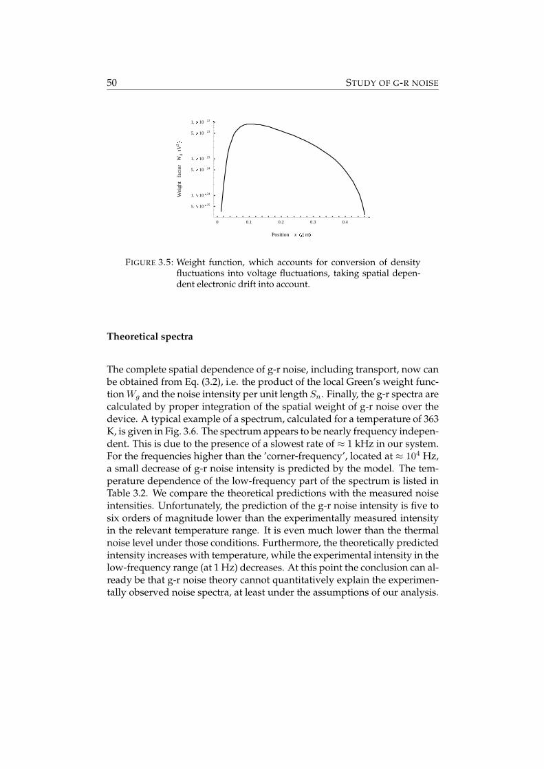
50 STUDY OF G-R NOISE
0 0.1 0.2 0.3 0.4
5. 10 25
1. 10 24
5. 10 24
1. 10 23
5. 10 23
1. 10 22
Position x m
thgieW
rotcafW
g V
2
FIGURE 3.5: Weight function, which accounts for conversion of densityfluctuations into voltage fluctuations, taking spatial depen-dent electronic drift into account.
Theoretical spectra
The complete spatial dependence of g-r noise, including transport, now canbe obtained from Eq. (3.2), i.e. the product of the local Green’s weight func-tion Wg and the noise intensity per unit length Sn. Finally, the g-r spectra arecalculated by proper integration of the spatial weight of g-r noise over thedevice. A typical example of a spectrum, calculated for a temperature of 363K, is given in Fig. 3.6. The spectrum appears to be nearly frequency indepen-dent. This is due to the presence of a slowest rate of ≈ 1 kHz in our system.For the frequencies higher than the ’corner-frequency’, located at ≈ 104 Hz,a small decrease of g-r noise intensity is predicted by the model. The tem-perature dependence of the low-frequency part of the spectrum is listed inTable 3.2. We compare the theoretical predictions with the measured noiseintensities. Unfortunately, the prediction of the g-r noise intensity is five tosix orders of magnitude lower than the experimentally measured intensityin the relevant temperature range. It is even much lower than the thermalnoise level under those conditions. Furthermore, the theoretically predictedintensity increases with temperature, while the experimental intensity in thelow-frequency range (at 1 Hz) decreases. At this point the conclusion can al-ready be that g-r noise theory cannot quantitatively explain the experimen-tally observed noise spectra, at least under the assumptions of our analysis.

3.3 CALCULATION OF G-R NOISE INTENSITY 51
1 10 100 1000 10000
5. 10 18
7. 10 18
1. 10 17
Frequency f Hz
lartcepSytisnetni
SV V
2
zH
1
FIGURE 3.6: G-r noise spectrum of an nin a-Si:H device at 363 K from Eq.(3.2).
T (K) SgrV /V 2 (Hz−1) Sexp
V /V 2 (Hz−1)340 5.8·10−18 5.9·10−12
363 9.9·10−18 3.9·10−12
402 1.9·10−17 1.2·10−12
434 2.6·10−17 7.8·10−13
TABLE 3.2: Noise intensities at 1 Hz, for g-r noise theory and experiment(B1).

52 STUDY OF G-R NOISE
3.4 Discussion of the model assumptions
Here, we critically discuss the choices and assumptions in the above analy-sis. First, the spatial dependence of the activation energy for the conductionwas taken in a parabolic approximation, which clearly deviates from the realsituation near the contacts. The same holds for the spatial dependence ofthe electrical field, which was self-consistently taken linear throughout thefilm. As one can see from spatial contributions of g-r noise, the contact re-gion (< 0.1 µm), however, contributes only weakly to the spectral intensity.Therefore, a better spatial approximation near the contacts will not changethe prediction.Second is the choice we made for the histogram of the defect levels. The lev-els close to the chemical potential are partially occupied, and significantlycontribute to the fluctuations. Indeed, from the computation of the noisecontributions from the various levels in our a-Si:H layer, we conclude thatlevels around the chemical potential dominate g-r noise. Support for ourchoice of the histogram comes from the theoretical work of Lee et al. [19]on a trap-rich semiconductor in absence of current. The detailed samplingaround chemical potential as we did, is indeed needed.Third, a specific choice of the defect concentrations determines the captureand emission rates, and indirectly the noise intensity. This represents an in-significant uncertainty in the predictions.We will proceed to discuss our quantitative results for the noise spectra in re-lation to earlier models and make a comparison with experimental data. Inour earlier work [41, 57] g-r noise was treated only phenomenologically andthe intensity was not computed. Our present theoretical prediction of rela-tive noise intensity at 1 Hz is much smaller than experimentally observed.Also the maximum value of the spatial weight function (the product of Sn
and Wg) deviates from the maximum of the phenomenological weight func-tion [57], which was adjusted to the fit the experimental noise spectrum.In retrospective, for the phenomenological approach an unrealistically largeweight was required. With the solution of the Green’s function in 2002 byVan Vliet [53] for an inhomogeneous device, we managed to compute theabsolute noise intensity for our device and found that the results are at vari-ance with the measurements. Even when all selected values of the deviceparameters would change by of a factor of 10, this conclusion still holds.As to the spectral shape, a white spectrum with a weak spectral decay iscomputed, while experimentally a 1/f spectrum is observed. This impliesthat g-r noise can not be the origin of the broad distribution of activation en-

3.4 DISCUSSION OF THE MODEL ASSUMPTIONS 53
ergies, obtained by Verleg and Dijkhuis [41] using the approach of Dutta,Dimon and Horn [18]. For the case n0 Ni, the spectral shape predicted byVan Vliet’s g-r noise theory [53] is a 1/f spectrum over at most two decades(in case of a flat distribution of states in the gap), both for homogeneous andinhomogeneous devices. We checked and confirmed that prediction withour program. In our case, however, n0 Ni in the central part of the de-vice, and n0 Ni only near the contacts, which results in a much broaderdistribution of activation energies, and thus in a nearly white spectrum.Finally, we note that with increasing temperature the slowest rate shifts tohigher frequencies exactly as the experimentally observed corner-frequency,defined in section 1.3 does [41]. However, the activation energy of the con-duction, being proportional to n0, equals that of the slowest rate. That isat variance with the experimental value for the corner-frequency, which is≈ 0.1 eV higher. Therefore the experimental ’fluctuation time’ [41] can notbe the relaxation time predicted by g-r noise theory, involving capture andemission of the conduction electrons at traps. In relation to this issue, the hy-pothesis that electron-hole recombination is responsible for the experimen-tally observed corner-frequency (see Ref. [41]) needs a critical discussion.The relaxation time of electron-hole recombination is exactly the same asfor g-r processes, since capture and emission rates determine the relaxation.On the contrary, the net recombination rate, which measures the number ofelectron-hole recombinations per unit time, is six orders of magnitude lowercompared to the total number of capture and emission events in our device.As a result, the noise intensity due to electron-hole recombination is evenbelow the intensity of g-r noise and cannot account for the measured inten-sity.This does not mean that g-r noise is always irrelevant. One could think ofsituations of different geometry, where g-r noise could well be a more dom-inant noise source. A reduction of device area would increase the chargeper unit area and the intensity of number fluctuations. G-r noise intensitywould therefore grow faster than other types of noise, which are only pro-portional to inverse area. Next, increasing the device length would lead toreduced band bending, which will lead to a stronger conversion of densityfluctuations into voltage fluctuations (Green’s weight function).

54 STUDY OF G-R NOISE
3.5 Conclusion and perspectives
In conclusion, g-r noise in an inhomogeneous multi-level system cannot ex-plain the observed noise spectra in nin devices of hydrogenated amorphoussilicon. Neither capture and emission processes, nor electron-hole recombi-nations are the direct origin of the observed noise spectra. The measuredintensities of 1/f noise and thermal noise exceed the theoretical predictionsby far.Leaving the geometry considerations for the moment, we are confrontedwith noise measurements without an explanation. Obviously, another noisesource is responsible for the observed fluctuations. That source should ex-hibit a broad distribution of energies, as found from the Dutta-Dimon-Hornapproach. That could be possible for a system with an energy distribu-tion broader than the typical energy width due to Fermi-Dirac statistics of≈ 4kBT . This was suggested by Baciocchi, D’Amico and Van Vliet [39], al-though they had no clue about the role of local potential fluctuations. Thenext chapter deals with such fluctuations, and considers charge fluctuationsof defects in the structure of the material as the origin of voltage fluctuations.

Chapter 4
Long-range potentialfluctuations
4.1 Introduction
In the 1980’s it has been recognized that electronic transport in amorphoussemiconductors is influenced by the presence of randomly located chargeddefects, which lead to a random potential landscape. Shklovskii and Efros[58] described a way to treat the electronic transport in a random potentiallandscape, in which screening plays an important role. A number of studiesillustrates the importance of potential fluctuations under various conditions[1, 59, 60, 61]. Our aim is to apply a theory of local potential fluctuations tohydrogenated amorphous silicon, in particular, to a nin a-Si:H structure sub-ject to a constant applied voltage perperdicular to the film, to determine theautocorrelation function of the voltage, and ultimately see if we can quanti-tatively explain the measured voltage noise.The potential landscape due to the amorphous structure is strongly disor-dered, largely because of the variation in bond angles and bond lenghts.X-ray diffraction measurements, which are sensitive to the average (near-est) neighbor distance, show however that there is order on a lenghtscale of1 nm [1]. Variation of the local potential landscape may produce localizationof electrons. The precise nature of the localization in a-Si:H is unclear. It isneither pure Anderson localization [62] nor a percolation transition. Never-theless, the typical magnitude of the fluctuations of the local potential canbe estimated to be 0.2 eV (see section 4.4), and is comparable to the energyassociated with the disorder of the network [1]. The corresponding local-
55

56 LONG-RANGE POTENTIAL FLUCTUATIONS
ization length is of the order of 1-10 nm. The amplitude of the fluctuationsdepends on the specific origin of the potential fluctuations. As said above,the main cause of the random potential is due to the amorphous structureof the material. The strongly disordered structure leads to bound localizedelectronic states below the mobility edge, known as the tail states. Note thateven above the mobility edge, the same random landscape may create lo-cally barriers of extra height for the emission of electrons from defects to theconduction band.Further, the random potential is due to charged deep defects. Deep de-fects in amorphous silicon are identified as dangling bonds (non-bound sil-icon orbits). The random location of the defects is schematically depictedin Fig. 4.1, in which + and − signs indicate the charge of the defect, whenpresent. The mean separation between charged defects is approximately 60
+
+
+
+
+
+
-
-
-
-
-
60 nm
FIGURE 4.1: Random positions of charged deep defects, usually denotedas D+,D0 and D− to distinguish between their charge. Therandom presence of opposite charge induces a random po-tential.
nm when two-third of the total defect density of 6·1015 cm−3 is taken to becharged [13]. In (near-) intrinsic material the free electrons are relativelyscarce and outnumbered far by the charged deep defects. As a result, thosedeep defects are not effectively screened by free electrons. The random dis-tribution of charged deep defects leads to a static random potential, whichis reduced by a self-screening mechanism, discussed in detail in section 4.2.3:if the charge on the defect fluctuates the surrounding defects respond byemitting or capturing electons and, as a result, screen the fluctuation of thelocal potential. Finally, a random potential can fluctuate because thermallyactivated capture and emission of charge on deep defects. The charge ondefects located in the window of ±kBT around the chemical potential willtypically fluctuate on the time scale of the emission time τe, which turns out

4.1 INTRODUCTION 57
to be in the millisecond range.This constitutes the physical background of 1/f noise from number fluc-tuations induced by two-level transitions with a distribution of activationenergies, similar to the model of Dutta, Dimon and Horn [18]. That modelis phenomenological and treats thermally activated transitions between twoenergy levels, and a barrier energy distribution that is broad on the scale ofkBT . In a number of materials (e.g. metal oxides [21], a-Si:H [41]) it turnedout to be a powerful description: the extracted energy distribution simulta-neously explains both the frequency and temperature dependence of the 1/fnoise. However, the model does not address the microscopic origin of thetwo-state systems and the mechanism by which they couple to the resistancefluctuations. As a result, the intensity of the noise remains an adjustable pa-rameter. The DDH-analysis was successfully applied to devices of a-Si:H byVerleg and Dijkhuis [41], resulting in 0.2 - 0.25 eV wide distribution of acti-vation barriers. At that time, the observations were interpreted as g-r noise.The broad distribution was explained by band bending or, alternatively, bya distribution of correlation energies. In Chapter 3 g-r noise was calculatedincluding band bending and a distribution of defects. The noise intensityturned out to be five to six orders of magnitude smaller than observed andthe explanation in terms of g-r noise thus failed.Arkhipov and Adriaenssens [60] considered slow random fluctuations ofgap-state energies producing typical 1/f noise characteristics in a-Si:H, dueto a distribution of thermal activation energies for carrier release out of deepstates. In their model a sinusoidal fluctuation of the conduction band edgeand a 1/f spectral dependence were assumed. Again, their model onlygives a phenomenological description and does not yield a quantitative re-sult, based on microscopic processes.The new theory we will use is a first-principle approach of the mechanismdescribed by Shklovskii and Efros [58], suggested by Arkhipov and Adri-aenssens for noise in a-Si:H, and mainly developed by B.V. Fine [63]. ThisChapter describes the essential ingredients of the model and contains a de-tailed comparison between theory and experiments on noise in a-Si:H nindevices.

58 LONG-RANGE POTENTIAL FLUCTUATIONS
4.2 Theory
4.2.1 Autocorrelation function
In case a constant current I0 is applied to a film with device resistance R, themeasured voltage V can be written as
V (t) = V0 + δV (t), (4.1)
where V0 is the average voltage (I0R) and δV (t) is the voltage fluctuation attime t. Using the Wiener-Khintchine theorem [15], the noise spectrum SV (f)of voltage fluctuations δV can be expressed as
SV (f)V 2
0
= 4∫ ∞
0CV (t)cos(2πft)dt, (4.2)
where the voltage autocorrelation function CV reads
CV (t) =〈V (t)V (0)〉
V 20
− 1. (4.3)
A constant applied voltage results in the term −1, which is removed in areal experiment due to the AC coupling by the amplifier. Therefore it canbe safely neglected in the rest of the treatment. We will connect the quantityof interest, the voltage autocorrelation function CV , to resistance fluctua-tions and finally to potential fluctuations within the material. Our deviceis connected in series to a relatively high resistance Rseries (see the setupin Fig. 2.5). Therefore, a constant applied voltage over the circuit resultsin a constant current I0 through the electrical circuit. In other words, cur-rent fluctuations are negligible. Further, all measurements were performedunder Ohmic conditions for the device. Therefore we can write
〈V (t)V (0)〉 = I2〈R(t)R(0)〉. (4.4)
Experimentally we observed SV (f)/V 2 to be independent of V , at least inthe Ohmic regime, which validates Eq. (4.4) in our experiments. The deviceresistance can be written as R(t) = R0 + δR(t), where R0 is the averagedevice resistance and δR(t) is the resistance fluctuation at time t. InsertingOhm’s law into Eq. (4.4) leads to
CV (t) =〈δR(t)δR(0)〉
R20
. (4.5)
The setup thus makes resistance fluctuations observable as voltage fluctua-tions, provided a constant current is flowing through the film.

4.2 THEORY 59
4.2.2 Single layer approach
The current flows perpendicularly to the plane of our µm-thin layered nin-structure (see Fig. 2.4). The presence of doped n-layers that electronicallyconnect the undoped intrinsic layer to the leads, induces band bending ofthe conduction band (see section 2.2.3), that can be approximated in the cen-ter (x=0) as EC(x) = EC0 − βx2, where β characterizes the strength of theband bending (see Eq. (2.1)). The typical value of EC(0), written as EC0, is0.63 eV above the chemical potential µ. The largest contribution to the filmresistance originates from the central part of the device. The fluctuationsnear the doped areas do not contribute significantly to the relative noise in-tensity, since that part has negligible resistivity due to band bending. Insection 2.2.4 we introduced a “uniform resistivity layer”, spreading alongthe x-axis between −xT and xT , to simplify matters and to faithfully ap-proximate the actual resistivity profile. The length of the uniform resistivitylayer reads
2xT =
√πkBT
β. (4.6)
Note that band bending is accounted for via β in the value of xT .The resistivity within the “uniform resistivity layer” fluctuates as a conse-quence of the fluctuation of the screened Coulomb potential φ(t, r) createdby all deep defects: When the potential φ(t, r) fluctuates, the electrons re-spond and track it, thus effectively EC(t, r) = EC0 + eφ(t, r), where e isthe electron charge, and EC0 characterizes the layer of uniform resistiv-ity.Therefore, a fluctuation of the local potential results in a correspondingchange of the activation energy for emission of a carrier from a trap aroundthe Fermi level, EC0 − µ, to which the local density of conduction electronswill adjust. Because of the strong band bending in the real situation, theinternal electrical field is large (E ≈ 1.5 · 104 V/cm), resulting in a carrierdrift time (≈ L/µnE) of less than 10−7 s. That shows that electron drift toand from the contacts is fast enough to be able to adjust to the fluctuat-ing EC(t, r) on the time-scale of our measurement (> 10−4 s). In summary,potential fluctuations give rise to a spatio-temporal dependent electron den-sity.The resistivity ρ is inversely proportional to the electron density (Eq. (2.2)).The resistivity can be used to rewrite the voltage autocorrelation functionCV in terms of the potential fluctuations φ. To do this, we represent the totalresistivity as
ρ(t, r) = ρ0 + δρ(t, r), (4.7)

60 LONG-RANGE POTENTIAL FLUCTUATIONS
where δρ(t, r) is a small deviation from the average resistivity ρ0 due to localpotential fluctuations. The resistivity fluctuations are accompanied by fluc-tuations δj(t, r) of the current density. The expression for the total currentdensity is
j(t, r) = j0xx + δj(t, r), (4.8)
with j0x = I/A in the x-direction, where A is the device area. Accordingto Ohm’s law, we have for the electric field E(r) = ρ(r)j(r). The potentialdifference accross the central layer of the device is given by the integral
V =1A
∫ xT
−xT
dx
∫A
dy dz ρ(x, y, z) jx(x, y, z), (4.9)
where we made use of the fact that the voltage drop is in the x-direction andtherefore may take the current as jx. Symmetry considerations set a con-stant potential value in the yz-plane at a fixed x-coordinate. The integrationvolume VT is limited by ±xT along the x axis and the edges of the film inthe yz-plane (total area A). Linearizing Eq. (4.9) with respect to δρ and δj weobtain
δV (t) =1A
∫VT
[δρ(t, r)j0x + ρ0δjx(t, r)]d3r. (4.10)
The integration of the second term in Eq. (4.10) yields zero by virtue of theconstraint that all current fluctuations in plane should cancel out, becauseof the continuity equation, which prescribes a constant current in the x-direction. Thus, with j0x = I/A, we obtain
δR(t) =δV (t)
I=
1A2
∫VT
δρ(t, r)d3r. (4.11)
We now write
ρ(t, r) ∝ exp
(EC0 + eφ(t, r) − µ
kBT
), (4.12)
which can be expanded provided |eφ(t, r)| kBT (which is to be con-firmed, in Eq. (4.41), to be a reasonable assumption)
δρ(t, r) ∝ eφ(t, r)kBT
exp
(EC0 − µ
kBT
)=
eφ(t, r)kBT
ρ0, (4.13)
where ρ0 defines the average resistivity. Now, we evaluate the autocorrela-tion function, Eq. (4.5), using R0 = 2xT ρ0/A (from section 2.2.4), and insert-ing Eq. (4.11) and Eq. (4.13), to obtain
CV (t) =
(e
2kBTxT A
)2 ∫VT
d3r
∫VT
d3r′〈φ(t, r)φ(0, r′)〉. (4.14)

4.2 THEORY 61
We note that the expression for CV in terms of spatio-temporal potentialfluctuations, is independent of resistivity ρ0, simply because resistance R0
and resistance fluctuations δR(t) are both proportional to ρ0. The next taskis to describe the screening mechanism and specify the deep defects in theundoped a-Si:H layer.
4.2.3 Screening
Weak screening of fluctuating charged defects is an important issue in ourtreatment, and is described by the theory of Shklovskii and Efros [58]. Thescreening length - the scale at which the Coulomb potentual due to the extracharge is reduced by a factor of 1/e - ranges from 0.1 to 0.5 µm in our device,as we will demonstrate below. First, we will introduce the concept of self-screening, and later we add the other, more obvious screening mechanism,i.e. screening by the contacts.We will not consider the static part of the Coulomb fluctuations here, butonly the fluctuating part that we hold responsible for the measured slowtimescale of fluctuations. Consider defects located in the gap in the win-dow of ±kBT around the Fermi energy, which fluctuate on the timescale τe
(the emission time from the Fermi level). These defects will be called activedefects, and are indicated in dark gray in Fig. 4.2. Their density nT is a frac-tion 2kBT/∆E of the total midgap defect density nD, where ∆E is the widthof the Gaussian distribution of midgap states. Electron emission or capturewill change the charge state of a defect, and as a result change the local po-tential. The defects will be treated as point charges, with a charge qi= -e forD−, +e for D+, and 0 for D0 (the three charge states of a defect were de-fined in section 1.1.2). The Coulomb potential caused by unscreened activedefects at a point r in space is (in CGS units according to the notation usedRef. [63])
V (r) =∑
i
qi
ε|r − ri| , (4.15)
where the sum is taken over some spatial grid, say of a size of 0.2 nm (wenote that this choice will not affect any resulting formula), ε ≈ 12 is thedielectric constant and ri the radius-vector of the center of the i-th grid ele-ment.Since V (r) is the sum of many small and random contributions, the mean

62 LONG-RANGE POTENTIAL FLUCTUATIONS
+
+
-
++-
+
--+
- +
-
+-
-
Rmax
+
+
++-
+
--+
- +
-
+-
-
+
+
++-
+
--+
- +
-
+-
-
-
FIGURE 4.2: Cartoon of a charge fluctuation of a D− defect, affecting thelocal potential, to which an active D0 or D+ defect (indicatedby gray filling) might respond within the emission time τe,and effectively screen the initial charge fluctuation.
squared average of this potential is given by
〈V (r)2〉 =∑
i
〈q2i 〉
ε2|r − ri|2 , (4.16)
where〈q2
i 〉 = nT vcge2, (4.17)
and vcg represents the volume of one element of the grid. In the last step thegeneral principle of statistical averaging for N particles was used: 〈N2〉 = N(Poisson statistics).
Self-screening
The next step is the introduction of a new variable R = r− ri, and, with thehelp of Eq. (4.52), to transform the sum in Eq. (4.16) into an integral
〈V (r)2〉 =〈q2
i 〉ε2
∫ Rmax
0
1R2
4πR2dR
vcg=
4πnT e2
ε2Rmax. (4.18)
The cutoff Rmax is introduced in the above integral, in order to prevent theintegral from diverging. The physical origin of this cutoff is as follows. Ifthe local potential fluctuates to a value lower than the average EC , the emis-sion probability of local defects will increase and reactions D− → D0 + eand D0 → D+ + e will occur. A local fluctuation of the potential will thus bepartly compensated by local feedback reactions. That compensation mech-anism, or self-screening, causes a significant decrease of the potential fluctu-ation experienced at the edge of a subvolume R3
max. Now we will demon-strate the existence of such a cutoff Rmax by a self-consistent procedure.

4.2 THEORY 63
The length scale Rmax is taken as the characteristic length scale of The rangeover which the individual potential fluctuations are felt, and 4π
3 R3max the
corresponding volume. In that typical volume there are NRmax = 4π3 R3
maxnT
active deep defects. Thermal fluctuations of these defects in a limited timespan will affect the occupation numbers of active defects. Consequently thepotential exprerienced at the border of the volume changes by a typical root-mean-square (rms) value of Vrms =
√〈V (r)2〉.As a result, the occupation number of the active defects will change, sincethe thermal emission rate 1/τe of the defects is affected by the energy bar-rier change due to the potential fluctuation, while the capture rate remainsconstant. Capture processes are determined by the collision probability ofconduction electrons with a fixed number of defects. The change in the emis-sion rate is
1τu
=1τe
∣∣∣∣∣exp
(±eVrms
kBT
)∣∣∣∣∣ ≈ 1τe
eVrms
kBT, (4.19)
where we assumed eVrms kBT , which will be shown to be valid in Eq.(4.23).A potential fluctuation thus drives the change in the occupation numbers ofthe defects via a change in the emission rate 1/τu. But after a time τe, thetypical equilibrium emission time (equal to the capture time), the occupationnumber on the average will be driven in the opposite way. Therefore, duringthat time τe, the number of active defects that will change their occupationnumbers in a systematic way is limited to:
∆NRmax = NRmax
[1 − exp
(− τe
τu
)]≈ NRmax
τe
τu=
NRmaxeVrms
kBT. (4.20)
The number of active defects is able to produce a feedback change in screen-ing the local potential amounting to e∆NRmax/εRmax, which is, using Eq.(4.20)
e∆NRmax
εRmax=
e2NRmaxVrms
εRmaxkBT= Vrms, (4.21)
and equals the (effective) root-mean-square potential evaluated at Rmax,Vrms. In this way, the procedure is made self-consistent, i.e. valid for aspecific combination of the screening radius and potential. In this example,the value of Rmax is obtained from condition Eq. (4.21) together with theexpressions for NRmax and nT , and using ε = 12, ∆E = 0.15 eV, and nD =
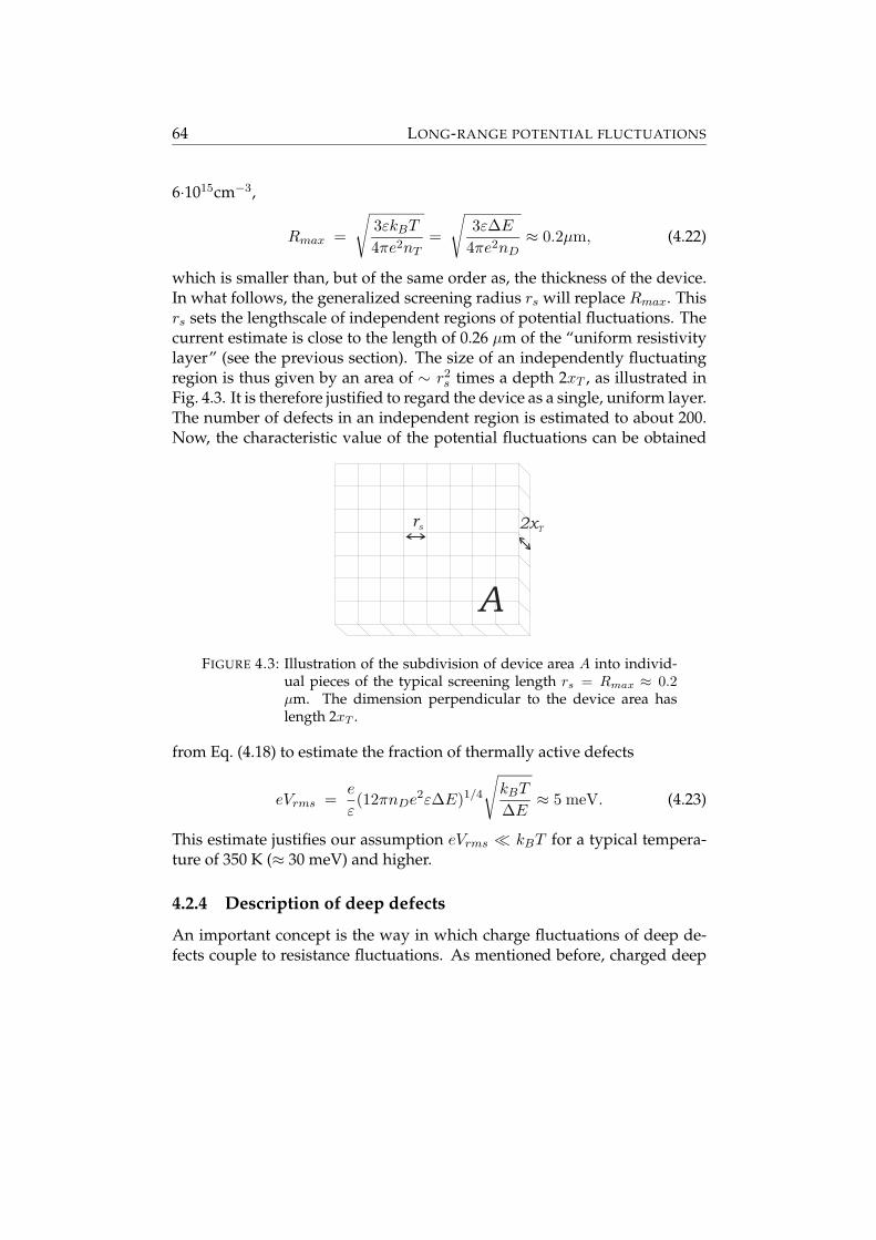
64 LONG-RANGE POTENTIAL FLUCTUATIONS
6·1015cm−3,
Rmax =
√3εkBT
4πe2nT=
√3ε∆E
4πe2nD≈ 0.2µm, (4.22)
which is smaller than, but of the same order as, the thickness of the device.In what follows, the generalized screening radius rs will replace Rmax. Thisrs sets the lengthscale of independent regions of potential fluctuations. Thecurrent estimate is close to the length of 0.26 µm of the “uniform resistivitylayer” (see the previous section). The size of an independently fluctuatingregion is thus given by an area of ∼ r2
s times a depth 2xT , as illustrated inFig. 4.3. It is therefore justified to regard the device as a single, uniform layer.The number of defects in an independent region is estimated to about 200.Now, the characteristic value of the potential fluctuations can be obtained
A
rs 2xT
FIGURE 4.3: Illustration of the subdivision of device area A into individ-ual pieces of the typical screening length rs = Rmax ≈ 0.2µm. The dimension perpendicular to the device area haslength 2xT .
from Eq. (4.18) to estimate the fraction of thermally active defects
eVrms =e
ε(12πnDe2ε∆E)1/4
√kBT
∆E≈ 5 meV. (4.23)
This estimate justifies our assumption eVrms kBT for a typical tempera-ture of 350 K (≈ 30 meV) and higher.
4.2.4 Description of deep defects
An important concept is the way in which charge fluctuations of deep de-fects couple to resistance fluctuations. As mentioned before, charged deep

4.2 THEORY 65
defects create a random potential landscape due to their random positions.Moreover, defects can switch between positive, neutral, and negative chargestates which induces fluctuations in the number of free electrons and is mea-sured as electrical noise. The energy levels E of the deep defects that char-acterize the transition D+ ↔ D0 can be assumed to be distributed accordingto a Gaussian profile p(E) around a central position E0 and a width ∆E
p(E) =1√
2π∆Eexp
[−(E − E0)2
2∆E2
]. (4.24)
The defect distribution p′(E′) that describes the transition D0 ↔ D− isshifted with respect to p(E) by a correlation energy U , which is requiredto put a second electron on a defect, and reads:
p′(E′) =1√
2π∆Eexp
[−(E′ − E0 − U)2
2∆E2
]. (4.25)
In intrinsic hydrogenated amorphous the average energy of E0 and E0 − Uis known to lie in the top half of the band gap. Further, in our device bandbending is considerable, and the chemical potential µ is somewhat closer toEC than for purely intrinsic material. The density of states in the center ofthe undoped layer is sketched in Fig. 4.4, based on fits with AMPS. We findthat µ almost coincides with the central position of the distribution p′(E′)associated with the transition D0 ↔ D−. Considering the 0.20-eV-differencebetween µ and p(E), much greater than 2kBT , transitions between D+ andD0 are rare and their contribution to the average fluctuation of charge ∆q isfound to be a negligibly small, 0.04 %. In the following, we shall thereforelimit ourselves to the description of transitions between D0 and D− states.In the calculations and in the paper [63], however, the two distributionswere both taken into account.To compute the average charge fluctuation 〈∆q2(E′)〉 due to defects, we thusconsider the part associated with the transition D0 ↔ D−, which was de-rived in the Appendix (section 4.6) and reads:
〈∆q2(E′)〉− =e2
4sech2
(E′ − µ
2kBT+ c
), (4.26)
where c = 12 ln2 and using sech2y = cosh−2y. Applying the statistical de-
scription of the occupation of defects presented in the Appendix, the prob-ability distribution for a charge fluctuation to be caused by a defect charac-

66 LONG-RANGE POTENTIAL FLUCTUATIONS
ECEV
P(E )B
Den
sity
ofst
ate
s
Energy
P(E )B p(E) p’(E’)
EB E
FIGURE 4.4: Schematic presentation of the density of states in the centerof the band gap, including extended states below the va-lence band edge EV and above the conduction band edgeEC , tail states within the band gap, and two Gaussian dis-tributions p(E) and p′(E′) with half-width ∆E representingdefect states. Gaussian distributions of activation energiesfor electron or hole emission from deep traps are depicted asP (EB), with a half-width ∆EB .
4.2 THEORY 67
terized by an energy E′ is
p′(E′) = p′(E′)sech2(
E′ − µ
2kBT+ c
). (4.27)
The fraction of defects, which exhibit substantial charge fluctuations, is ex-pressed as ν(T ) and reads
ν(T ) =1
4kBT
∫ ∞
−∞p′(E′)dE′, (4.28)
where p′ represents the active (i.e. those within ∼ 2kBT around µ) part ofthe defect distribution. To account for the total width of the applied Fermifactor, the expression is scaled by 4kBT . The active defects mentioned beforeare now expressed as nDν(T ), representing the fraction of defects whichinduces the fluctuating part of the Coulomb potential. The product nDν(0)corresponds to the density of the defect states at the chemical potential. Wenote that ν(T ) is only weakly temperature dependent.
4.2.5 Activation barriers
We will proceed by examining the activation barriers for emission of trappedelectrons. The activation barrier EB is simply defined as the energy differ-ence between the chemical potential and the local value of the conductionband EC . Due to the random network, there is medium-range disorder on thelength-scale of 1-10 nm, resulting in a distribution of activation barriers. InFig. 4.5 a cartoon of this disorder is given. The best description for activationbarriers in an amorphous material is again perhaps a Gaussian distribution.A Gaussian distribution of width ∆EB centered around an average barrierheight EB0 reads
P (EB) =1√
2π∆EB
exp[−(EB − EB0)2
2∆E2B
]. (4.29)
The central energy, EB0, and width, ∆EB , of P (EB) turn out to be the onlyadjustable parameters of this theory. The distribution of activation barriers forelectron is represented in Fig. 4.4 by a Gaussian distribution around positionEB0 with a half-width ∆EB . Holes are assumed to experience the mirrorimage of that distribution below the valence band.

68 LONG-RANGE POTENTIAL FLUCTUATIONS
1 nm
EB
E
ECE
nerg
y
Position
FIGURE 4.5: Cartoon of the potential barriers due to the random networkand to the random positions of deep defects.
4.2.6 Rates and rate equations
The presence of a distribution of activation barriers in the material impliesthat electron emission rates are distributed as well. We will end up with aconvolution over the barrier energies and the defect energies in our compu-tation of the noise spectrum. Van Rheenen et al. [64] described the fluctua-tion rate 1/τ− for the D0 ↔ D− transition
1τ−(E′, EB)
= ω0(EB)[12e−EB−µ
kBT + e−EB−E′
kBT
]. (4.30)
Here, the factor 12 originates from the degeneracy of the D0 state and ω0 is
the so-called attempt rate, which can be written as
ω0 = σvthNC(EB). (4.31)
Here σ = 10−15cm2 is the capture cross section, vth is the thermal veloc-ity of electrons, which amounts to 3·107 cm s−1 at room temperature, andNC(EB) is the effective density of states above the mobility edge, the prod-uct of kBT and the empirical value of NC(EB) of 1.5·1022 eV−1cm−3. Atypical value of ω0 is therefore ∼ 1013 s−1. The density of states abovethe mobility edge was fitted empirically to the data reported in Ref. [1],using NC(EB) = NC(EC0)
√(EB − EC0 + εC)/εC , where we evaluated at
EB − EC0 = 0.27 eV (as will result from the fit to data of device B1) andfound εC = 0.02 eV.The presence of a distribution of activation barriers creates a broad range of

4.2 THEORY 69
fluctuation times in the system. If a specific defect fluctuates on time scaleτ , its potential can only be screened by those defects fluctuating on timescales equal or smaller than τ . The slower defects react - on the average -too slow, keep their charge and do not contribute to the screening. There-fore, the number of active defects which responds fast enough is expressedas nDν(T )b(τ), with the fraction b(τ) defined as
b(τ) =1
4kBTν(T )
∫E−(τ)
p′(E′)P (EB)dE′dEB, (4.32)
where E−(τ) is the subspace of the E, EB-space which satisfies the conditionτ−(E′, EB) < τ . The thermal prefactor 4kBT enters both in b(τ) and in ν(T ),and therefore cancels in the expression for the generalized screening radiusrs2, deduced from Eq. (4.22):
rs2(τ) =√
ε
4πe2nDν(T )b(τ). (4.33)
The screening due to defects in the undoped layer is one important screen-ing mechanism in our system. The other mechanism is provided by thedoped n-layers and contacts. Doping creates a relatively large concentrationof free electrons in the n-layers, which provides a metallic type of screening:a (fluctuating) defect in the undoped layer is screened by its mirror images,constructed with respect to the mirror planes located at x = ±d/2 (the inter-faces between the doped and undoped layers).The resulting potential is calculated, and the screening radius is determinedas the distance between the location of the defect and the point where thevalue of the bare Coulomb potential is reduced by a factor 1/e (where e isthe base of the natural logarithm). In Fig. 4.6 a sketch the anisotropic natureof this screening mechanism is indicated. The screening in the yz-plane istaken equal in y- and z-direction. The computation of the screening in thex-direction is more involved for a defect located off-center, since one needsmultiple image-charges. The situation for a defect located at x = 0, however,can be dealt with using only two mirror images. We computed rsx = 0.38d,and rsy = rsz = 0.54d. On the basis of our sketch, we estimate the screeningradius due to the n-layers as
rs1 = (rsxrsyrsz)1/3 ≈ 0.48d. (4.34)
A typical value of this screening radius is rs1 = 0.43 µm. In principle, thetwo screening mechanisms act simultaneously and independently, and add

70 LONG-RANGE POTENTIAL FLUCTUATIONS
1 0.5 0 0.5 1
0.4
0.2
0
0.2
0.4
Position y m
noitisoP
x
m
FIGURE 4.6: Anisotropic screening of a charged defect in the origin due tocharge in the n-layers and contacts, located at x±0.5µm. Only2µm of the 7 mm total length in the y-direction is plotted. Thecontour between the light and dark gray area indicates theposition where the bare Coulomb potential is reduced by afactor of 1/e due to screening.
up. The net effect of the two mechanisms leads to a reciprocal screeningradius
1rs(τ)
=1
rs1+
1rs2(τ)
. (4.35)
In order to estimate the value of this screening radius, one needs the detailsof the defect distribution.
4.2.7 From potential fluctuations to noise
The Coulomb potential of a fluctuating charge ∆q at coordinate a is screened,resulting in a potential
φ(t, r) =∫ ∆q(t,a)
ε|r − a| exp(−|r− a|
rs
)d3a. (4.36)
To calculate the electrical noise in Eq. 4.14, the autocorrelation function ofthe potential fluctuations, 〈φ(t, r)φ(0, r′)〉, needs to be known. In order tobe able to compute the autocorrelation function, we note that individualdefects fluctuate independently, and take the disorder average. Thereforewe can safely assume that the correlation does not depend on the (random)position a of the defects, resulting in
〈φ(t, r)φ(0, r′)〉 =〈∆q(t)∆q(0)〉
ε2F (r, r′, τ). (4.37)

4.2 THEORY 71
Here F (r, r′, τ) is approximated using the assumption that the correlationdepends only on the relative distance |r − r′| as
F (r, r′, τ) ≡∫ exp
(− |r−a|+|r′−a|
rs(τ)
)|r − a||r′ − a| d3a (4.38)
≈ 2πrs(τ)exp(−|r − r′|
rs(τ)
). (4.39)
Further, for a charge fluctuation ∆qi characterized by a fluctuation time τi,we have 〈∆qi(t)∆qi(0)〉 = 〈∆q2〉exp(−t/τi), and consequently, for the actualrange of fluctuation times τ− in Eq. (4.37):
〈φ(t, r)φ(0, r′)〉 =nD
ε2
∫ ∫dEBdE′P (EB)p′(E′)F (r, r′, τ−(E′, EB))
〈∆q(E′)2〉−exp(− t
τ−(E′, EB)
). (4.40)
¿From a general perspective, it is interesting to know what the amplitude ofthe potential fluctuations actually is. Recall that we assumed it to be belowkBT ≈ 30 meV to justify the approximation made for the local resistivityfluctuations in Eq. (4.13). The amplitude of |eφ(t, r)| has been estimatedusing Eq. (4.40) as:
e√〈φ2(0, 0)〉 ≈ e2ε−1
√2πnDν(T )kBTr∗s ≈ 3.5meV, (4.41)
and since |eφ(t, r)| kBT , the fluctuation of resistivity δρ is sufficientlysmall.So far the theoretical treatment applied to transitions of the type D0 ↔ D−,which will appear to give the main contribution to the calculated noise un-der the condition E′
0 ≈ µ. As mentioned above, the contributions from theD+ ↔ D0 at energy E should be added in the expressions for the fluctua-tion time, the screening radius, and the charge fluctuation correlation func-tion (see Ref. [63]). In the calculations, both distributions were taken intoaccount. In our situation this gives a slight improvement (< 1%) with re-spect to a calculation with a single distribution p′(E′). The full expressionfor the noise is obtained by taking the Fourier transform of the autocorrela-tion function of φ (Eqs. (4.14) and (4.40)). It includes the expression for thefluctuation time τ+, analoguous to Eq. (4.30), and further 〈∆q2〉 in Eq. (4.54)resulting in:
SV (f)V 2
=2π2e4nD
ε2(kBT )2Ax2T
∫dEB P (EB)

72 LONG-RANGE POTENTIAL FLUCTUATIONS
×[∫
D(f, τ+(E, EB)) p(E)dE +∫
D(f, τ−(E′, EB)) p′(E′)dE′]
, (4.42)
where
D(f, τ) =τr4
s(τ)[4xT − 3rs(τ) + e
− 2xTrs(τ) (2xT + 3rs(τ))
]1 + (2πfτ)2
. (4.43)
The Lorentzian spectrum τ/(1+(2πfτ)2) in D originates from Fourier trans-formation of the exponential decay function in time which characterizes thecharge fluctuations (see Eq. (4.40)), while the restriction of the integrationspace by the area A and the length of the uniform resistivity layer xT , re-sults in the form r4
s [. . .] and is responsible for the other terms in Eq. (4.43).A quantitative analysis is carried out using Eq. (4.42). For the qualitativeanalysis we can reduce Eq. (4.42) to a more transparant expression for thenoise spectrum, by taking the limits xT rs, valid for the faster fluctuationprocesses, and kBT ∆EB , and finally approximating the number of ac-tive defects by the kBTnD/∆E, which sets ν(T ) = 1
2∆E , and approximatesthe Gaussian defect distribution to a flat one of width ∆E. In these limits,the theoretical expression for the noise reads
SV (f)V 2
=8π2e4nD
ε2kBT∆EA
∫τ(EB)r3
s(τ(EB))P (EB)dEB
1 + (2πfτ(EB))2. (4.44)
Note that in this approximation the fluctuation time τ does not depend onE′ nor E anymore:
τ(EB) =32ω0(EB)exp
(−EB − µ
kBT
). (4.45)
In contrast to the case of g-r noise (see Eq. (3.2)), the resulting expression isindependent of the number of conduction electrons. Further, the inverse propor-tionality of the noise to area A is very common, since takes the number offluctuators in a volume into account. The dependence on the concentrationof deep defects is only weak: the nD dependence of the prefactor is balancedby the 1/
√nD dependence of rs2, which constitutes a part of the screening
radius rs and which enters as r3s in Eq. (4.44). Due to the proximity of the
n-layers, and the resulting value of rs1 which competes strongly with rs2 inthe relevant low-energy region, the nD-dependence of the noise intensity iseven weaker than 1/
√nD.
In summary, this theory provides a quantitative prediction for both the pref-actor of the noise and the distribution of energy barriers which is eventuallyresponsible for the electrical noise.

4.3 TEMPERATURE DEPENDENCE 73
4.3 Temperature dependence
The theory of long-range potential fluctuations results in an equation for anoise spectrum which depends on temperature. In this section noise spectrain a broad temperature range are presented and analyzed with the theory ofpotential fluctuations. The emerging fitted distribution of potential barriers,responsible for the fluctuations is discussed.
4.3.1 Noise spectra
The temperature dependence of conduction and noise was measured for thedevices specified in Tab. 2.1. The qualitative behavior of our a-Si:H nin de-vices is in accordance with earlier work in our group [41]. The expectedinverse proportionality of the noise intensity on device area was verified ex-perimentally.All measurements described in this section were carried out on device B1at 50 mV in the Ohmic regime. The temperature was varied from 295 K upto 434 K, the higher bound in order to avoid out-diffusion of hydrogen andstructural rearrangements, the lower bound because below room tempera-ture the device has a too large resistance for carying out low-frequency noisemeasurements.
In Fig. 4.7 we present a set of noise spectra for a range of temperatures,which are shifted by 303, 302, and 30 to separate them from each other;scale refers to the 340-K-spectrum. The theoretical curves, using the de-vice parameters mentioned in the previous sections, are included in Fig. 4.7.The prefactor of the theoretical noise intensity in Eq. (4.42) is directly deter-mined, without adjustable parameters, from the known device parameterssuch as area, defect density, the characteristic length of band bending xT ,and the temperature T . Our main result is that the theoretical prediction ofthe noise intensity is of the right magnitude for all temperatures. We stressagain that the theory has only two adjustable parameters: the width ∆EB
and the central position EB0 - µ of distribution of potential barriers. Theseparameters only influence the spectral shape, but not the intensity. The spec-tral shape and its temperature dependence all fit very well. Below, the fittedvalues for ∆EB and EB0 will be discussed.

74 LONG-RANGE POTENTIAL FLUCTUATIONS
1 102 104
f [Hz]
340 K
362 K
402 K
434 K
10- 14
10- 12
10- 10
10- 8
SV/V
2[s
](a)
FIGURE 4.7: Noise spectra measured in the Ohmic regime, at 50 mV. Er-ratic lines indicate experimental data and smooth lines pre-dictions of Eq. (4.42), to real scale for T=434 K. Spectra at 340K, 362 K, and 402 K are multiplied by 303, 302 and 30, respec-tively, to make them distinguishable. When all plotted on thesame scale, difference in intensity are less than one order ofmagnitude.

4.3 TEMPERATURE DEPENDENCE 75
4.3.2 Distribution of potential barriers
The parameters of P (EB), the Gaussian probability distribution of poten-tial barriers in the conduction band, is extracted from the data given in Fig.4.8. The peak EB0 is at 0.90 eV above µ and the width ∆EB = 0.09 eV. Since
0.6 0.7 0.8 0.9 1.1 1.2 1.3EB eV
0.01
0.02
0.03
0.04
0.05PEBeV
1
FIGURE 4.8: The Gaussian distribution of emission barriers as experi-enced by electrons in deep traps. The chemical potential µis set to zero. The central position EB0 and the width ∆Ewere adjusted to obtain the curvature which fits best to thedata.
EC0 − µ = 0.63 eV, we arrive at EB0 − EC0 = 0.27 eV. According to AMPSsimulations (see Table 2.2, the B1 device parameter nD is (6 ± 2) ·1015cm−3
and E′0 = µ± 0.02 eV. As a consequence, the values of EB0 and ∆EB are
subject to an error of 20 %.The screening radius rs is plotted in Fig. 4.9 in the relevant energy range ofEB . For high energy barriers, a larger fraction of the defects can respond fastenough to screen local potential fluctuations, resulting in a smaller screen-ing radius. For low energy barriers the screening is only by the n-layers witha corresponding screening radius of ∼ 0.4 µm.In Fig. 4.10, we present as a full line the weight distribution function r3
sP (EB).This function weighs the contribution to the noise from transitions charac-terized by a barrier of EB and corresponding to a transition time τ and aLorentzian noise spectrum τ/(1+(2πfτ)2) (see Eq. (4.44). This weight func-tion has a shift of the peak energy of ≈ 0.1 eV relative to the maximum of

76 LONG-RANGE POTENTIAL FLUCTUATIONS
0.6 0.7 0.8 0.9 1.1 1.2 1.3EB eV
0.1
0.2
0.3
0.4
rsm
FIGURE 4.9: Screening radius, composed of screening by the free chargein the n-layers and by the self-screening mechanism of the(charged) defects. The self-screening mechanism depends onthe characteristic time τ of electron emission from deep de-fects and thus on the barrier height EB .
P (EB) and an asymmetrical distribution in energy.
4.3.3 Dutta-Dimon-Horn analysis
The temperature dependence of the noise spectra in a-Si:H was first ana-lyzed by Verleg and Dijkhuis (see section 1.3 and Ref. [41]). The changein the spectral curvature with temperature results in a shift of the so-calledcharacteristic frequency f1, which is the frequency where the slope of thespectrum equals -1. When temperature is increased, the increase of f1 ap-pears to be thermally activated. The activation energy of the characteristicfrequency for the nin device B1 is 0.81 ± 0.03 eV (see section 1.3).The results of DDH analysis on the same data of device B1 are included inFig. 4.10 in order to compare it with the distribution r3
sP (EB), the weightfunction of the present theory. Their shapes are identical, although theirmaxima are shifted slightly. We note that in case of DDH analysis the en-ergy scale depends very much on the Arrhenius fit to the characteristic fre-quency f1 vs temperature. The energy shift is therefore attributed to thatunavoidable uncertainty. Clearly our theory provides a microscopic basis

4.3 TEMPERATURE DEPENDENCE 77
0.6 0.7 0.8 0.9 1.0 1.1 1.20.0
5.0x10⁻⁵
1.0x10⁻⁴
1.5x10⁻⁴
2.0x10⁻⁴
2.5x10⁻⁴
3.0x10⁻⁴
3.5x10⁻⁴
10 Hz 100 Hz theory
Energy EB - µ (eV)
Effec
tive
dis
trib
uti
on P
(EB) r
s3(E
B)
FIGURE 4.10: Effective distribution of emission barriers device B1 mea-sured at V = 50 mV. In good approximation, the distributionof barriers responsible for the curvature of the spectrum isthe original barrier distribution weighted by the screeningradius cubed. The effective distribution is peaked at a bar-rier energy which corresponds to the activation energy ofthe characteristic frequency f1 in the noise spectrum. Forcomparison, the distribution of activation energies obtainedwith Dutta-Dimon-Horn analysis (see section 4.3.3) is in-cluded.

78 LONG-RANGE POTENTIAL FLUCTUATIONS
for the phenomenological distribution obtained from the DDH analysis.The distribution of the barriers peaks above the conduction band edge. Weclaim that this is the explanation for the fact that the activation energy inthe noise spectra exceeds the conductivity activation energy by 0.18 eV. Weconclude that the previous assumptions [41] that noise is governed by holedynamics is wrong.
4.3.4 Discussion of Dutta-Dimon-Horn analysis
In Verleg’s analysis, the asymmetry in the DDH distribution function couldnot be explained. An asymmetric weight function now appears naturallyfrom the theory of random potential fluctuations. According to our theory,the reason why a spectrum close to 1/f is observed is explained by the dis-tribution of barrier heights in a random potential landscape. The theoryallows for a quantitative prediction of the noise intensity, while in the DDHapproach, the noise intensity is an adjustable parameter. It is noted thatthe 1/T dependence of the prefactor in Eq. (4.44) is a feature of the poten-tial fluctuations theory, which apparently predicts the observed decrease ofnoise intensity with increasing temperature rather well. Also in this respect,the theory works better than the DDH approach, in which the temperaturedependence of the prefactor is proportional to T . The mismatch of DDH-analysis for the temperature dependence of noise intensity in a-Si:H deviceswas not noticed before, since the noise prefactor is free to chose in that ap-proach.
4.4 General discussion
The theoretical spectra are accurate within a factor of two, due to a numberof uncertainties in the estimates. The attempt frequency ω0 and the screen-ing function F (r, r′, τ) are accurate within a factor of two. Further uncer-tainty was introduced by the errors in the AMPS determination of the defectparameters nD, ∆E, and E0. Given the margin of the theoretical prediction,there is good agreement with the experimental noise spectra.We now give two rough estimates, of the localization length of electrons andof the typical length scale of the medium-range disorder of the amorphousstructure from the fitted distribution of emission barriers. Fig. (4.5) showsschematically a narrow deep energy well, of energy EC0 − E, and a widershallower well. First, the localization length of an electron near an active

4.4 GENERAL DISCUSSION 79
defect can be determined by the well depth E, equated to µ, and reads
λ =
√h2
m∗e(EC0 − µ)
, (4.46)
where h is Planck’s constant divided by 2π. In a-Si:H the minimal local-ization length is approximately 0.5 nm. For a better estimate, one shouldconsider the competition between activation over the barrier and tunnelingthrough the barrier. Second, the same equation can be applied to the barriersin the potential landscape. This gives an estimate of the “penetration depth”of electrons, and is determined by replacing µ by the local barrier height EB
in Eq. (4.46), taking the absolute value, which turns out to be around ∼ 0.2eV, resulting in a “penetration depth” of the barrier in the range from 1 to 10nm. Also in this second estimate, still the issue will remain whether tunnel-ing is faster of slower then the activation over the barrier.From a practical point of view, our analysis introduces a new method ofcharacterizing the deep defects in a-Si:H. In particular, our finding, thatEB0 − EC0 is 0.27 ± 0.05 eV, which is substantially greater than 0.1 eV -the scale of potential fluctuations seen in the drift mobility experiments [1]- may indicate that the defects are not distributed randomly in the back-ground of the medium-range potential but, instead, located in the regionsof greater local strain, i.e. around the peaks of that potential. On the otherhand, there is no principal need for a symmetric distribution of barriersaround the mobility edge. Therefore it could simply be the result of anasymmetric distribution.This work is not the first in the field of spatio-temporal fluctuations of a ran-dom potential landscape. There are other convincing indications in litera-ture of the existence of strong temporal fluctuations in the potential land-scape of disordered materials. In several papers of Arkhipov and Adri-aenssens [59, 60] random potential landscapes were modeled in terms of adistribution of activation energies. However, they did not attempt to derivea quantitative expression for the noise intensity, leaving the noise intensityas an adjustable parameter.Our experimental results all refer to sandwich devices and Gaussian noise[41] and thus may have a different cause than the non-Gaussian 1/f -noisereported by Kakalios and co-workers obtained in coplanar devices whichwere interpreted in terms of a limited number of fluctuating filaments [25,27, 65]. Both in case of coplanar and sandwich devices, however, the noise isproduced by temporal carrier fluctuations induced by changes in the local

80 LONG-RANGE POTENTIAL FLUCTUATIONS
potential. The coplanar structure studied, leads to non-Gaussian noise, be-cause current has to go via long paths, which are very sensitive to the localpotential. Charge fluctuations can cause current filaments to switch on andoff, resulting in a noise intensity which changes with time. In sandwich geom-etry the area through which current flows is very large and the filaments,if any, are extremely short and numerous. As a result, the noise becomesuncorrelated, or Gaussian (see Ref. [41]). The time dependence of the noiseintensity and thus the non-Gaussian behavior is therefore absent in our con-figuration. In summary, in a coplanar structure a local charge fluctuationcan cause switching of filaments, while in a sandwich structure it can leadto a potential fluctuation on a time-scale related to electron emission of deepdefects.Finally, we discuss the results of Gunes, Kasap and Johanson on coplanar a-Si:H films (see section 1.3.2) briefly in the light of the theory of potential fluc-tuations. The noise intensity, measured in a small frequency interval 1 Hz -1 kHz, is comparable to ours. The strict power-law dependence reported atthe lower frequencies might show a deviation at higher frequencies, whichis not measurable due to the presence of a second noise mechanism.
4.5 Conclusion
The noise spectra in nin a-Si:H sandwich structures based on the theory ofpotential fluctuations are in good agreement with the experimental data.In particular, the change of the curvature as a result of variation of tem-perature is reproduced. The microscopic theory presented in this Chapterthus leads to a quantitative expression for 1/f noise. That is a quite sig-nificant achievement in the field of 1/f noise, which, in many cases, is de-scribed only phenomenologically, in particular by Hooge’s empirical law.Our theory provides the microscopic origin of the observed noise and goesbeyond the phenomenological Dutta-Dimon-Horn (DDH) model to explain1/f noise. Furthermore, the theory predicts the intensity of the noise withno adjustable parameters. The noise mechanism proposed is quite generaland only requires the presence of charge traps in regions of poor screening.
4.6 APPENDIX: EQUILIBRIUM STATISTICAL DESCRIPTION 81
4.6 Appendix: Equilibrium statistical description
The equilibrium occupation numbers of the D+, D0 and D− states of a defect[66] are, respectivily,
feq+ =
1Z
, (4.47)
feq0 =
2exp(−E−µ
kBT
)Z
, (4.48)
and
feq− =
exp(−2E+U−2µ
kBT
)Z
; (4.49)
where
Z = 1 + 2 exp(−E − µ
kBT
)+ exp
(−2E + U − 2µ
kBT
). (4.50)
The average electric charge of the defect is
〈q〉 =e
Z
[2 exp
(−E − µ
kBT
)+ 2 exp
(−2E + U − 2µ
kBT
)], (4.51)
where e is the elementary electron charge. The mean squared value of thecharge is
〈q2〉 =e2
Z
[2 exp
(−E − µ
kBT
)+ 4 exp
(−2E + U − 2µ
kBT
)]. (4.52)
Thus the mean squared charge fluctuation is
〈∆q2(E)〉 ≡ 〈q2〉 − 〈q〉2
=2e2
Z2
[exp
(−E − µ
kBT
)+ 2 exp
(−2E + U − 2µ
kBT
)
+exp(−3E + U − 3µ
kBT
)]. (4.53)
Since exp(− UkBT ) 1 for all temperatures in the experiment, we can ap-
proximate the above expression as
〈∆q2(E)〉 =e2
4
[1
cosh2(
E−µ2kBT − c
) +1
cosh2(
E+U−µ2kBT + c
)], (4.54)

82 LONG-RANGE POTENTIAL FLUCTUATIONS
introducing the statistical constant c = 12 ln2, which results from the de-
generacy of the D0 state. Furthermore, the two parts in the expressionare associated with the two kinds of transitions, as they follow each fromindependent treatment from those transitions. As a result, we have forthe charge fluctuations associated with the D0 ↔ D− transitions, usingsech2y = cosh−2y,
〈∆q2(E′)〉− =e2
4sech2
(E′ − µ
2kBT+ c
). (4.55)

Chapter 5
Further experimental evidencefor the role of long-rangepotential fluctuations in themechanism of 1/f noise ina-Si:H
5.1 Introduction
We present measurements of 1/f resistance noise in two different films ofamorphous silicon (a-Si) and compare the results to the nin a-Si:H devicestudied so far. One of the newly studied films has a nin structure with then-layers hydrogenated as well, while the intrinsic layer was deuterated. Theother film has a pip structure with all three layers hydrogenated. These de-vices provide a means for new experimental tests of our recent theoreticalproposal [63] explaining the origin of low frequency resistance noise in hy-drogenated amorphous silicon (a-Si:H).Usually, this kind of noise has a spectral shape close to 1/f , where f is fre-quency. Our theory was fully developed for µm-thick films in the presenceof a electric current perpendicular to the plane. It explained the resistancefluctuations by linking them to the thermal fluctuations of the occupationnumbers of deep charged defects identified as dangling bonds. The noisemechanism involved the fluctuations of the long-range Coulomb potentialcreated by those defects. The 1/f -like spectral shape was related to the dis-
83

84 FURTHER EXPERIMENTAL EVIDENCE
tribution of potential barriers limiting the charge carrier escape from deepdefects. This theoretical picture is amenable to a first-principle calculationof the integrated noise intensity. It also yields the prefactor in front of the1/f frequency dependence. In the previous Chapter we studied 1/f noisein an nin structure of a-Si:H . In that structure the resistance noise originatedfrom the middle of the undoped layer, where electrons are the majority car-riers. In this Chapter these spectra are compared to that of the pip deviceand deuterated device.The above mentioned theory implies two clear predictions. First, it shouldbe directly generalizable to the case of pip structure, where holes are themajority carriers in the middle of the undoped layer. In Ref. [63], it was as-sumed that the distribution of the potential barriers for electron escape fromdeep defects is related to the medium range disorder of the local potentialaround the defects. This type of disorder should not be much different forthe holes with respect to the valence band edge EV as compared with thatof the electrons with respect to the conduction band edge EC . Therefore,the natural expectation is that: (i) our theory should give correct 1/f noiseintensity for pip structures and (ii) if the samples are grown under identicalconditions, the distribution of the potential barriers obtained from the stud-ies of pip structures should be nearly the same (if counted from EV ). Wetest the above prediction on a pip structure, grown in the same reactor andunder similar conditions as the nin structure studied in Chapters 2, 3 and 4.The second theoretical prediction is that, if the mechanism of charge fluctu-ations on deep defects is correctly identified in previous Chapter with theescape and the capture of carriers, then the 1/f noise spectrum should notdepend on the substitution of hydrogen with its heavier isotope deuterium- subject of the other test presented in this Chapter.Potentially, the “deuteration” test can also distinguish the mechanism ofdefect charge fluctuations due to the emission and the capture of chargecarriers from another one associated with the diffusion of hydrogen atoms.This diffusion mechanism can create or annihilate the dangling bonds. Sucha mechanism will certainly depend on the substitution of hydrogen withheavier deuterium. Unfortunately, the quantitative theory of 1/f noise asso-ciated with hydrogen diffusion is lacking. In principle, it is possible, that theisotope substitution affects only the activation prefactors of hydrogen diffu-sion, which would have only a very small effect on the resulting noise inten-sity; or, otherwise, it can also affect either the activation energies and/or thecoupling to the observed noise variable φ(r, t), in which case the “isotopeeffect” should be more noticeable.

5.2 DEVICES 85
To apply the theory described in Chapter 4 to the hole conduction noise inpip structures, the energy axis should be reversed, EC and EC0 should bereplaced with EV and EV 0, respectively, and effective electron mass shouldbe replaced by effective hole mass. In this way, all variables describing theD+ ↔ D0 transition will describe the D0 ↔ D− transition and vice versa.
5.2 Devices
In this section, the most important device parameters, partly covered inChapter 2, are given. The first device, B1, is the nin film of a-Si:H , thesame as reported in Chapter 4. The second device, C, is the pip structure ofa-Si:H . The third device, D1, is the nin structure, where the undoped layerwas deuterated, while the n-layers were hydrogenated. The amorphous sili-con layers were all grown by Plasma Enhanced Chemical Vapor Deposition(PECVD) at an RF field of 13.56 MHz and a substrate temperature of 468K. The intrinsic layer of thickness di and area A was sandwiched betweeneither ∼ 50-nm-thick n-type layers or, in case of device C, 28-nm-thick mi-crocrystalline p-type layers. Doped crystalline silicon wafers were used as asubstrate, and the top contact consisted of Ti/Cu layers. Further details ofdeposition and devices can be found in Table 5.1 and section 2.1.
The energy distribution of deep defects was modelled by two Gaussians,
nin B1 pip C nin D1di (µm) 0.91 0.84 1.12A (cm2) 0.55 0.57 0.57nD (cm−3) 6·1015 6·1015 4·1015
E0 − µ (eV) -0.2 0.0 -0.2β (eV/µm2) 1.59 1.54 1.24
TABLE 5.1: Devices parameters, defect density nD, defect energy E0
and band bending parameter β from AMPS analysis of J-V -curves.
shifted with respect to each other by the correlation energy U = 0.2 eV.One of the Gaussians described the D+ ↔ D0 transition and the other oneD0 ↔ D− transition. We applied the one-dimensional device simulationprogram AMPS [48] to fit to the measured current-voltage characteristicsand thus obtained the concentration of deep defects nD, the band bendingcoefficient, β, and the positions of the maximum of the first of the above

86 FURTHER EXPERIMENTAL EVIDENCE
Gaussians E0. The best fit was obtained for the values of the defect pa-rameters reported in Table 5.1. The half-width of the Gaussian distribution∆E was fixed at 0.15 eV, the bandgap at 1.80 eV, the carrier mobility at 10cm2V−1s−1, the capture cross sections at 10−15 cm2, effective electron massat 0.4 me, effective hole mass at me, and the density of states at the mobilityedge at 4·1021 eV−1cm−3. The values of EC0 − µ for the nin devices andEV 0−µ for the pip devices were obtained from the temperature dependenceof the resistivity.We measure the voltage noise spectra at frequencies in the range from 1 to104 Hz and in the temperature range 340 K 434 K. All calibrated spectrawere taken at 50 mV, in the Ohmic regime, and are the result of averagingover 300 individual spectra. The expected inverse proportionality of thenoise intensity on device area was found experimentally. Further details ofour experimental setup are described in Ref. [41].
5.3 Experimental results
pip a-Si:H device. The noise mechanism for holes is tested using the pip a-Si:H device. The noise spectra are curved 1/f -like spectra, with a character-istic frequency f1 that is thermally activated (see Fig. 5.1). The experimentalactivation energy EBexp of frequency f1 equals 0.94 ± 0.04 eV. The quali-tative behavior of the noise spectra in Fig. 5.2 turns out to be analogous tothat of nin devices. The theoretical curves were calculated using Eq. (4.42)but now for the hole transitions to and from charged deep defects. The in-tegrated noise intensity is determined from the numbers given in Table 5.1and 5.2 and in section 5.2. The central position EB0 of the Gaussian distribu-tion of defects P (EB) and its width ∆EB are the only adjustable parameters.They govern the curvature of the noise spectra. The theoretically predictednoise spectra, which have a accuracy of a factor of two, are in good agree-ment with the measurements. We note that the measured activation gap tothe conduction band Eσ,nin < Eσ,pip, caused by the fact that intrinsic a-Si:His slightly n-type. Because of the larger conductivity activation energy Eσ,the input value for EB0 - µ in pip devices is 0.15 eV larger than the corre-sponding value for nin devices (see Table 5.2 and Fig. 5.3). However, whencounted from the valence mobility edge, the value of EB0−EV 0 is very closeto EB0 - EC0 for the nin device B1. The values of ∆EB for the two devicesare also in reasonable agreement. For this device (and for the two others),the peak of the effective distribution EBdist coincides with the experimental
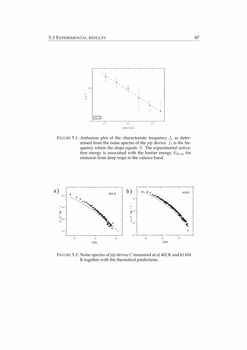
5.3 EXPERIMENTAL RESULTS 87
2.3 2.4 2.51
10
f1
f 1 (s-1
)
1000/T (K-1)
FIGURE 5.1: Arrhenius plot of the characteristic frequency f1 as deter-mined from the noise spectra of the pip device: f1 is the fre-quency where the slope equals -1. The experimental activa-tion energy is associated with the barrier energy EBexp foremission from deep traps to the valence band.
a) b)
100 101 102
10-15
10-14
10-13
10-12
f (Hz)
SV /V
2 (H
z -1
)
434 K
100 101 102
10-14
10-13
10-12
10-11
f (Hz)
SV /V
2 (H
z -1
)
402 K
FIGURE 5.2: Noise spectra of pip device C measured at a) 402 K and b) 434K together with the theoretical predictions.

88 FURTHER EXPERIMENTAL EVIDENCE
B1, nin C, pip D1, nin with Dσ0 (Ω−1m−1) (2.3 ± 0.5)·104 (7 ± 1)·103 (1.7 ± 0.5)·104
Eσ (eV) 0.63 ± 0.03 0.82 ± 0.03 0.67 ± 0.03f0 (Hz) (2.3 ± 2.8) · 1012 (2 ± 4) · 1012 (4 ± 13) · 1012
EBexp(eV) 0.81 ± 0.03 0.94 ± 0.04 0.88 ± 0.04EBdist − µ (eV) 0.81 ± 0.06 0.98 ± 0.06 0.86 ± 0.06EB0 − µ (eV) 0.90 ± 0.05 1.05 ± 0.05 0.99 ± 0.05EB0 − EC0 (eV) 0.27 ± 0.05 0.23 ± 0.05 0.32 ± 0.05∆EB(eV) 0.09 ± 0.02 0.07 ± 0.02 0.11 ± 0.02
TABLE 5.2: Energy barriers and their corresponding prefactors for con-duction and noise, respectively. The first four parameters areobtained experimentally. Below the line: fitted energy barriersand widths from theory.
-0.5 0.0 0.5 1.0 1.5 2.0 2.50.0
2.0x10⁻⁴
4.0x10⁻⁴
6.0x10⁻⁴
pip (C) H nin (B1) D nin (D1)
P (E
B )
r s3 (E
B )
(eV
-1 µ
m3)
Energy EB - EV (eV)
FIGURE 5.3: Effecitve distribution of emission barriers of pip device (C)below EV and deuterated nin device D1 above EC . For com-parison, the distribution of nin device B1 is included.

5.3 EXPERIMENTAL RESULTS 89
activation energy EBexp of the characteristic noise frequency (defined in Ref.[41]), as it should.Another parameter accessible from the experimental noise data is the prefac-tor f0, determined from the Arrhenius plot of the characteristic frequency f1
(see Table 5.2). For device C, B1 and also for device A the result is the about2 · 1012 Hz. This compares well with the theoretical attempt frequency fromEq.(4.31): f0 = ω0/2π ≈ 1.6 · 1012 s−1.
nin a-Si:D device. Typical spectra for device B1 (passivated with hydro-gen) and device D1 (passivated with deuterium) are shown in Fig. 5.4.There is virtually no difference between noise spectra from devices with
100 101 102 103
10-15
10-14
10-13
10-12
10-11
f (Hz)
SV /V
2 (H
z -1 )
402 K B1 D1
100
101
102
103
10-15
10-14
10-13
10-12
10-11
f (Hz)
SV /V
2 (H
z -1 )
402 K B1 D1
d)c)
b)a)
100 101 102 103
10-15
10-14
10-13
10-12
10-11
f (Hz)
SV /V
2 (H
z -1
)340 K
B1 D1
100 101 102 103
10-15
10-14
10-13
10-12
10-11
f (Hz)
SV /
V 2 (H
z -
1 )
340 K B1 D1
FIGURE 5.4: Noise spectra measured at a) 340 K and c) 402 K for devicesB1 and D1, which contain H and D, respectively. The theoret-ical predictions for the devices are plotted in (b) and (d) usingthe parameters of the Gaussian distribution of barriers, listedin Table 5.2.
hydrogen or deuterium in the temperature range from 295 K to 350 K. Elec-

90 FURTHER EXPERIMENTAL EVIDENCE
tronically, the devices are identical, but have a 23 % difference in thickness(see Table 5.1). In the theory, this results in a slightly higher noise inten-sity for the deuterium device predominantly in the low-frequency region inthe temperature range from 350 K to 434 K. Given the agreement betweenexperiment and theory, we conclude that the main reason for the small dif-ference of the curvature between the two devices lies in the difference inthickness, which induces an increase of the screening radius in the deu-terium device. The barrier distribution for this device is characterized bythe values of EB0 −EC0 and ∆EB , which are close to the values of the sameparameters obtained for the hydrogenated device.
5.4 Conclusion
We have measured the 1/f noise spectra in nin and pip a-Si:H devices and inan nin a-Si:D device. In all three cases, we have found a very good quantita-tive agreement between the experiments and the theory proposed in Chap-ter 4. The theory is valid both in the regime, where electrons are the majoritycarriers (nin devices), and in the regime, where holes are the majority carri-ers (pip device). The comparison of the results gives further support for theexistence of a universal distribution of emission barriers in a-Si:H /D for thecarrier escape from deep defects.The maximum of that distribution is located approximately 0.27 eV abovethe conduction band or valence band mobility edges for electrons and holes,respectively. The width of this distribution is about 0.09 eV. Comparing theresults for the deuterated and hydrogenated devices, we observed no sig-nificant difference, which was also consistent with the theory.

Chapter 6
Noise study of degradation
6.1 Motivation
Metastability of a-Si:H is still an important scientific issue, several decadesafter the discovery of the Staebler-Wronski effect (SWE) in 1976. It was ob-served that the defect density increases upon light soaking [6]. There hasbeen a long dispute about the microscopic origin of the SWE. Questionswere raised about if and how far hydrogen atoms would diffuse after thebreaking of a Si-H bond. And how saturation of the defect density wouldbe reached. Recent developments in the field of metastability of a-Si:H werediscussed in section 1.1.3. In this Chapter we examine the effects of degra-dation on the resistance noise. With the microscopic theory developed inChapter 4, it is possible to explain changes in the noise spectra upon pro-longed illumination by microscopic changes in the local potential. As inChapter 4 and 5, the input device parameters are obtained from analysis ofconductivity data. The theory of long-range potential fluctuations predictsa very weak dependence on the defect density nD: a slight increase by a fac-tor of ∼ 1.2 for the given increase in nD (see section 6.4.4). The theoreticalprediction, however, is at variance with explorative experimental results ondegradation effects on the noise spectra obtained by Verleg [41].
91
92 NOISE STUDY OF DEGRADATION
6.2 Measurements on silver-epoxy contacted devices
6.2.1 Measurement conditions
The first part of the degradation study was carried out on devices with simi-lar contacts as the devices used by Verleg, while the second part of the studyis on devices with wire-bonded contacts. In the first case, a silver-epoxy wasused as a connection between the Ti/Cu top-contact and the Cu wire, andbetween that wire and a gold pad on the ceramic substrate (see Fig. 2.1).Devices were degraded in subsequent steps using 0.2 W/cm2 irradiationfrom a halogen lamp, which is filtered to emit predominantly in the visi-ble. For comparison: the intensity of the sun corresponds to 0.1 W/cm2. Aninfrared filter was used to prevent the device from heating and a lens to fo-cus the light on a few square cm and to irradiate the complete device area.After each degradation step, the conductivity and noise were measured inabsence of light. The hydrogenated nin device in this study is device B1,the properties of which are described in Chapter 4, while the deuterated nindevice D1, which was treated in Chapter 5. It was observed that using deu-terium instead of hydrogen as passivators did not affect the resistance noiseand other electronic properties of the material. Another deuterium device(D3) was made with aluminum bonded contacts, which appears to reducethe effect of degradation on the change in the conductivity. We refer to theoriginal state of these devices as the ’annealed state’.
6.2.2 Effect of degradation
It is generally accepted that the defect density increases rapidly in the firststage of degradation, subsequently slows down, and finally reaches a satu-ration value. As a result, the device resistance increases and saturates. Thedevices B1 and D1 were degraded in four and two steps, respectively, untilsaturation was achieved. Deuterated amorphous silicon is known to haveslower degradation kinetics [67], and was therefore illuminated longer and,in the second step, with twice as much intensity. For a good comparison,the integrated irradiated energy is used as the measure for the degradationin Table 6.1. The reduction in dark conductivity after the last degradationstep is a factor of 6 and 12 for device B1 and D1, respectively. This dif-ference is mainly caused by a the higher amount of irradiated energy ondevice D1. Before presenting the noise data, the concept ’variance’ is intro-duced. Variance of a fluctuating quantity a is defined as var(a) = a2 − a2.
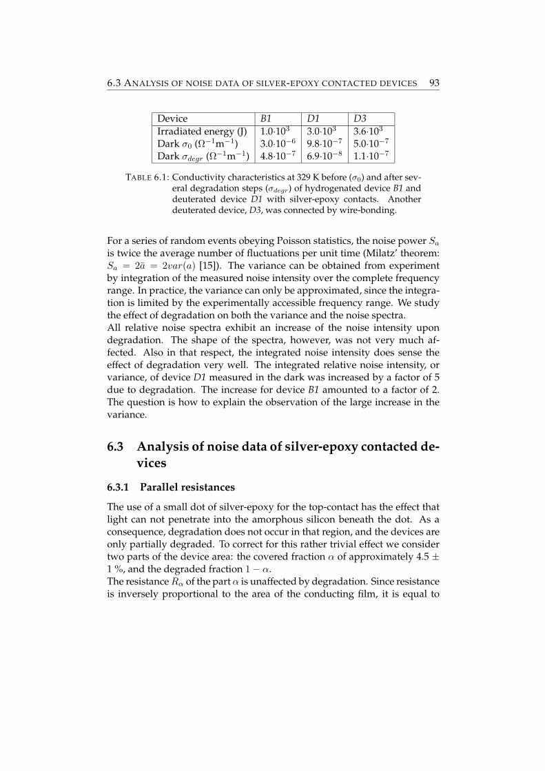
6.3 ANALYSIS OF NOISE DATA OF SILVER-EPOXY CONTACTED DEVICES 93
Device B1 D1 D3Irradiated energy (J) 1.0·103 3.0·103 3.6·103
Dark σ0 (Ω−1m−1) 3.0·10−6 9.8·10−7 5.0·10−7
Dark σdegr (Ω−1m−1) 4.8·10−7 6.9·10−8 1.1·10−7
TABLE 6.1: Conductivity characteristics at 329 K before (σ0) and after sev-eral degradation steps (σdegr) of hydrogenated device B1 anddeuterated device D1 with silver-epoxy contacts. Anotherdeuterated device, D3, was connected by wire-bonding.
For a series of random events obeying Poisson statistics, the noise power Sa
is twice the average number of fluctuations per unit time (Milatz’ theorem:Sa = 2a = 2var(a) [15]). The variance can be obtained from experimentby integration of the measured noise intensity over the complete frequencyrange. In practice, the variance can only be approximated, since the integra-tion is limited by the experimentally accessible frequency range. We studythe effect of degradation on both the variance and the noise spectra.All relative noise spectra exhibit an increase of the noise intensity upondegradation. The shape of the spectra, however, was not very much af-fected. Also in that respect, the integrated noise intensity does sense theeffect of degradation very well. The integrated relative noise intensity, orvariance, of device D1 measured in the dark was increased by a factor of 5due to degradation. The increase for device B1 amounted to a factor of 2.The question is how to explain the observation of the large increase in thevariance.
6.3 Analysis of noise data of silver-epoxy contacted de-vices
6.3.1 Parallel resistances
The use of a small dot of silver-epoxy for the top-contact has the effect thatlight can not penetrate into the amorphous silicon beneath the dot. As aconsequence, degradation does not occur in that region, and the devices areonly partially degraded. To correct for this rather trivial effect we considertwo parts of the device area: the covered fraction α of approximately 4.5 ±1 %, and the degraded fraction 1 − α.The resistance Rα of the part α is unaffected by degradation. Since resistanceis inversely proportional to the area of the conducting film, it is equal to

94 NOISE STUDY OF DEGRADATION
R0/α, where R0 is the total device resistance in the annealed state. The totaldevice resistance R in a degraded state depends further on the value Rd ofthe uncovered part, which is connected in parallel to the covered part, andreads
R =RαRd
Rα + Rd. (6.1)
The relationship between resistance and degradation time td is Rd ∝ t−1/3d
according to experiments and to the solution of a proper set of kinetic equa-tions [8]. Using Eq. (6.1) we find a power law dependence of Rd on td of -0.32 ± 0.03, in accordance with the value mentioned above.
6.3.2 Extraction of the degradation term in the noise
Now we consider resistance fluctuations in a device which is locally de-graded, and we treat resistance fluctuations in the degraded part δRd(t) andresistance fluctuations in the non-degraded part δRα(t). The time develop-ment of the device resistance R(t) in a state of degradation is now includedas an average value R and a fluctuating part δR(t). Linearizing R(t), thefluctuations in both parts give
δR(t) =R2
α
(Rα + Rd)2δRd(t) +
R2d
(Rα + Rd)2δRα(t). (6.2)
The quantity of interest is the autocorrelation function of fluctuations in R:〈δR(t)δR(0)〉. It can be expressed in terms of autocorrelation functions ofboth parts, as in Eq. (6.2), with the prefactors properly squared. There isno cross correlation term between the two parts, due to the separation inspace. In order to compute the voltage noise power, we apply Ohm’s law,V = IR, which implies δV = IδR under constant current conditions of theexperiments, use Eq. (6.1) for R, and obtain:(
SV
V 2
)αd
=R2
α
(Rα + Rd)2SRd
R2d
+R2
d
(Rα + Rd)2SRα
R2α
. (6.3)
Here the noise power SV of a quantity V denotes the Fourier transformof the autocorrelation function 〈δV (t)δV (0)〉. The measured noise relativeintensity upon partial degradation (denoted by suffix αd) consists of twocoupled terms. To separate these terms, the degradation-independent noiseterm from the covered part is expressed in the measured voltage noise inten-sity of the annealed state
(SVV 2
)0. Again using Ohms’ law, we have SR/R2 =

6.4 MEASUREMENTS IN WIRE-BONDED DEVICES 95
SV /V 2 [15]. Reminding that noise intensity is inversely proportional to area,and thus to α, we obtain SRα
R2α
= 1α
(SVV 2
)0. Rewriting Eq. (6.3) results in:
(SVd
V 2d
)αd
=(Rα + Rd)2
R2α
(SV
V 2
)αd
− 1α
R2d
R2α
(SV
V 2
)0
. (6.4)
The expression is frequency independent, and therefore also applies to theintegrated noise intensity (or variance).
6.3.3 Noise data of degraded part
The examination of the noise contributions from the covered and the un-covered parts tells us that in early stages of degradation, the total resistanceis dominated by the uncovered part, and this part contributes greatly to thenoise. Further, as light soaking continues, and the resistance of the degradedpart increases, the resistance of the uncovered part becomes comparable tothe (high) resistance of the small column of material below the silver dot.Then the total variance gradually will be taken over by the covered part. Inthe limiting case Rd → ∞, no current will pass the degraded part and thenoise intensity is increased by a factor 1/α, i.e. equal to the reduction of area.The correction results in a smaller increase of the integrated noise intensityupon degradation than observed in the raw data.Fig. 6.1 shows the dependence of the variance on the degradation time forthe raw data and for the degraded part only of the sample. Due to uncer-tainty in the measurement of the covered fraction α of the area, the predic-tion of the true effect of degradation varies between no effect for a coverageof 0.055 to an increase for a coverage of 0.035. In the degraded part both thespectral shape and the variance changed only by a relatively small amount.Now we will describe devices in which those small effects can be studied tobetter advantage.
6.4 Measurements in wire-bonded devices
Although the use of silver epoxy for the contact connections is a good choiceto avoid contact noise, even the smallest dot which is possible, will coversuch an area, that large corrections are needed in analyzing noise measure-ments due to degradation. To reduce the covered area by the contact, weused the technique of wire bonding to provide the electrical contact between

96 NOISE STUDY OF DEGRADATION
103
104
10-10
3x10⁻¹⁰
<< (annealed state)αd
(SV /V 2 )αd total device
(SVd
/Vd
2 )αd degraded part with 0.045 of area covered
Inte
grat
ed in
ten
sity
td (s)
FIGURE 6.1: Variance of the a-Si:H device B1 for the raw data from theentire device, and for the recalculated data, related to the de-graded part, for a covered fraction of 0.045. The light grayregion indicates the range of the predicted variance, giventhe uncertainty in the area of the covered part.
the top layer and the gold pad. We used an aluminum wire of 125-µm thick-ness and length of 1 mm. The value of the covered area fraction α is 0.002,a value for which the degraded part dominates the conduction and noise inthe full range of degradation stages. The remaining part of the degradationstudy was performed on a nin a-Si:D device (D3) from the same batch as thedevices D1 and D2.The rest of this Chapter will contain the characterization of this device invarious stages of degradation. In the analysis with our model we need val-ues for the defect density in subsequent stages of degradation. For that pur-pose, we apply and discuss two methods to the J-V characteristics. TheAMPS simulation program is used to trace back the defect density by fittingto the non-linear part of the J-V curve. Alternatively, the Space-Charge-Limited-Current method (SCLC) is applied to that feature to arrive at thedefect density. In section 6.4.4 we will present the degradation results, anddiscuss then in the light of the theory of long-range potential fluctuations.
6.4.1 Measurement conditions
The device conductivity was determined in the linear part of the J-V char-acteristics (see Fig. 6.3) after each degradation step, in the temperature range

6.4 MEASUREMENTS IN WIRE-BONDED DEVICES 97
from 295 K to 434 K. The activation energy of the conductivity Eσ for the de-vice in the annealed state is 0.67 ± 0.01 eV, equal to that of D1 and D2. Onlyafter the last stage of degradation, the activation energy showed a slight in-crease to 0.70 ± 0.03 eV.The degradation experiments were identical to those of section 6.2, exceptthat a cutoff filter was placed in the beam which only transmitted light ofwavelengths above 645 nm. Light of these wavelenghts (which correspondsto energies of the band gap and lower) has a relatively low absorption co-efficient, and therefore a large penetration depth. As a result, the opticalexcitation within the layers of amorphous silicon is homogeneous, in con-trast to earlier measurements. As a consequence, recombination of electronsand holes, which induces degradation, is almost uniform.The conductivity, measured after subsequent degradation steps , is plottedin Fig. 6.2. The conductivity has a power-law dependence on degradationtime, with a power 0.21 ± 0.04, close to the value of 0.25 for deuterated de-vices reported in literature [67]. After a number subsequent degradationsteps the device broke down.
10000
10-5
4x10⁻⁶
σ (Ω
-1m
-1)
t (s)
FIGURE 6.2: Conductivity of device D3 vs degradation time.
6.4.2 Device simulations
The one-dimensional simulation program for amorphous silicon devicesAMPS-1D [48] is used to determine the density of the deep defects beforeand after the last stage of degradation. The idea was to determine the de-vice parameters which fit best to the J-V characteristics of the device in the

98 NOISE STUDY OF DEGRADATION
annealed state, and subsequently to adjust exclusively the defect densityand mobility to obtain an equally well fit of the J-V curve in the last stageof degradation. The obtained defect density after degradation will then beused as the higher border in theoretical calculations of the noise spectra.The measured J-V characteristics are given in Fig. 6.3 together with thebest fits of the AMPS simulation program. The non-linearity is smaller afterdegradation, due to a larger space charge density. The simulation programyields the defect density. As input, the following quantities were used: a
0.01 0.1 1
10-4
10-3
10-2
10-1
annealed state degraded state simulations
Voltage (V)
Cu
rren
t d
ensi
ty J
(m
A/cm
2)
FIGURE 6.3: J-V characteristics of device D3 before and after light soak-ing. For both cases the device parameters (see Table 6.2) wereobtained by the best fit using AMPS.
band gap Eg of 1.80 eV, a correlation energy U of 0.2 eV, a width of 0.15 eVof the deep defect distributions, a capture cross section σ of 10−15 cm2, andthe measured layer thicknesses (see Table 2.1). The fit to the data in the an-nealed state was obtained using an electron mobility µn of 8 cm2V−1s−1, aDOS NC(EC) of 5·1019 cm−3, and a central position of the deep defect dis-tribution E0 located 0.17 eV below the Fermi level. As a result of the fit, thedeep defect density was determined at 6·1015 cm−3, and the band bendingparameter β at 0.85 eV/µm2.Next, to fit to the non-linear part of the J − V curve of the device in the de-graded part, all parameters were kept constant, except the defect density nD
= 1.0·1016cm−3 and µn = 7.2 cm2V−1s−1. The decrease of the electron mo-bility compared to the annealed state is plausible. As a result, we obtained0.69 eV for Eσ after degradation. From the AMPS simulations of the data,the relative increase of the defect density after degradation is found to be a

6.4 MEASUREMENTS IN WIRE-BONDED DEVICES 99
factor of 1.7 (see Table 6.2).
method annealed degradedAMPS 6.0·1015 cm−3 1.0·1016 cm−3
SCLC 6.8·1015 cm−3 1.1·1016 cm−3
TABLE 6.2: Defect density before and after degradation of device D3 usinga white light source. The two applied methods are describedin the text.
6.4.3 SCLC analysis
The SCLC method is a simple technique to determine the defect densityfrom the non-linearity in the J-V curve [68]. We ensured that the voltageand current determination (of the data in Fig. 6.3) were accurate enough tocalculate a reliable defect DOS according to the requirements in Ref. [69].With the known length L of the intrinsic layer and temperature T , and tak-ing ε = 12ε0 for a-Si:H, the defect density was determined in a relativelysmall energy range, where it was constant. Just as in the defect model inAMPS, we assume a Gaussian distribution of defects with a halfwidth ∆E= 0.15 eV. The SCLC result is in correspondence with the AMPS result (seeTable 6.2), and confirm the increase of the defect density upon degradationby a factor of 1.7. The AMPS values will be used in the theoretical predictionof the noise spectrum after degradation.
6.4.4 Noise measurements in wire-bonded devices
The effect of degradation on the noise spectra appeared to be minute: thespectral shape was unaffected while the intensity increased only by 10 %,as was found from integration over a reasonable frequency range. In Fig.6.4 the noise spectra before and after degradation are plotted. The remark-able part of this observation is that resistance increases (see Fig. 6.2) whilethe noise intensity does hardly change, while in other kinds of experiments(e.g. temperature variation) a change in the resistance is usually accompag-nied by a change of the noise intensity. The long-range potential fluctuationtheory is applied to describe the noise spectra in the annealed and degradedstages, which differ in the defect densities and band bending parameters.The AMPS results for the defect density nD and band bending parameter βwere inserted into the theoretical calculation to produce predictions, illus-trated in Fig. 6.5 for the annealed state and the last stage of degradation,

100 NOISE STUDY OF DEGRADATION
100
101
10-14
10-13
10-12
10-11
Frequency f (Hz)
SV
/V
2 (H
z-1)
annealed state degraded state
FIGURE 6.4: Noise spectra before and after prolonged light soaking. Thedifference is so small that the noise spectra of the intermedi-ate steps are not shown. Measured at 329 K with 50 mV biasvoltage and in absence of light.
respectively. Other input parameters taken after AMPS analysis were theenergies with respect to the chemical potential: EC − µ = 0.70 eV; E0 − µ= -0.14 eV. In theory, the Gaussian distribution of emission barriers governsthe spectral slope of the noise spectra. Since experimentally the curvaturedid not change significantly, the central energy EB0 − µ and the width ∆EB
were kept constant to their values of the annealed state (0.90 and 0.09 re-spectively).Before and after degradation, the theoretical predictions for the shape agreevery well with the data, and for the variance, at least within a factor of two,which is the accuracy of the theoretical prediction. On the basis of the the-ory, one would expect only minor changes in noise intensity and curvature,as observed.
6.5 Conclusion
The effect of prolonged illumination in an nin wire-bonded device (withsmall contact area) produced a factor of 1.7 increase of the defect densityand a relative increase of the noise intensity by only 10 % at 329 K. The spec-tral shape remains the same. The results for the degraded part of a silver-epoxy contacted device are in correspondence with these observations in a

6.5 CONCLUSION 101
1 10 100 1000 10000
1. 10 16
1. 10 14
1. 10 12
Frequency f Hz
esioN
ytisnetniS
V V
2
zH
1
FIGURE 6.5: Theoretical predictions using the defect density from analy-sis with AMPS as an input parameter. The solid line is cal-culated using the value obtained for the annealed state, thedashed line indicates the spectrum of the degraded state. Forcomparison, data of the degraded state are included.
wire-bonded device. The theoretical predictions of the noise spectra are inaccordance with the data, when the defect density as obtained from AMPSsimulations is inserted for a limited range of defect densities.The theory of long-range potential fluctuations as a mechanism for 1/f noiseseems to predict the weak effect of degradation on the noise intensity prop-erly. We recommend to redo the experiment, but with a longer degradationtime to confirm our observations in a larger range of defect densities. Fromthe constancy of the spectral shape we tend to conclude that degradationdoes not change the electronic energy of the defects nor their distributionin energy. To put it differently, a confirmation of this experimental studymight tell that the medium-range order probed by noise measurements isnot affected by degradation.


Chapter 7
Diffusion noise in TFTs
7.1 Introduction
The invention of the bipolar transistor - the first electronic switch - has beenof crucial importance for the development of information technology. Incomputers for example, one will find the follow-up of the bipolar transis-tor, the field-effect transistor (FET). The current in a FET runs from sourceto drain, and is controlled by a gate, usually formed by a Metal-Oxide-Semiconductor (MOS) structure. The voltage applied at the gate of a MOS-FET creates a conduction channel.
7.1.1 Thin-film transistors
The production of a modern version of the transistor, the thin-film transis-tor (TFT), is attractive because of low material costs and flexible design ofdevices, owing to etching techniques. The expensive c-Si substrate used inMOSFETs can be replaced by glass, which is cheap and allows for large-areadepostion. The gate electrode in a TFT is separated from the conductingchannel by a thin insulating layer (see Fig. 7.1). The gate voltage generatesan electrical field at the insulator-semiconductor interface, to which elec-trons in the semiconductor respond. Variation of the gate voltage inducesa change in the electron density near the interface, which can be used toeffectively switch the resistance of the channel. Nowadays, such thin-filmtransistors (TFTs) are applied in active matrix displays, better known as flatpanel displays, described in Ref. [70]. The transistors of our study consist ofthin films of hydrogenated amorphous silicon (a-Si:H).
103

104 DIFFUSION NOISE IN TFTS
7.1.2 1/f noise in the on-state of TFTs
In transistors 1/f noise is generally observed. Measurements have been re-ported on crystalline MOSFETs [71], on amorphous silicon [72, 73, 74], andpolycrystalline silicon thin-film transistors [75, 76]. These measurementswere invariably performed in the Ohmic regime and, of course, as a func-tion of gate voltage. In Table 7.1 an overview of TFT noise studies is given.All mentioned transistors exhibit 1/f noise in the on-state, have a top-gate
Device W (µm)/L(µm) Noise Authorsc-Si MOSFET 24/12 1/f noise Xu et al. [71]a-Si:H TFT 10/4 to 400/32 1/f noise Valenza et al.[72]a-Si:H TFT 15/15 to 240/15 1/f noise Boudry et al.[77]Polysilicon TFT 50/10 to 50/3.5 1/f noise Dimitriadis et al.[75]Polysilicon TFT 10/10 1/f noise Angelis et al.[76]Polysilicon TFT 150/75 to 400/4 1/fα noise Deen et al. [78]
0.8 < α < 1.2
TABLE 7.1: Overview of earlier noise studies in TFTs.
configuration and a ratio W/L ranging from 1 to 100. A quite different classof transistors, polymer TFTs of poly-thienylene vinylene (PTV) revealed 1/fnoise as well [79]. Usually the 1/f noise is described by Hooge’s empiricallaw for voltage noise SV [80]
SV (f)V 2
=αH
Nf, (7.1)
where N is the number of free carriers and αH a proportionality constant,which appears to be approximately 10−5 to 10−4 in c-Si [72] and 10−2 ina-Si:H [72, 74]. In PTV samples the values of αH are in the range of 0.01-0.08 [79]. In Ref. [81] a model is discussed which incorporates both numberfluctuations and surface mobility fluctuations, that was later extended to in-clude trapping noise with correlated mobility fluctuations [82]. In the lattercase, trapping of charge carriers on oxide traps near the oxide-semiconductorinterface leads to charge fluctuations which in turn affect the interface car-rier mobility. All these measurements were performed well above thresh-old. We are aware of only one paper reporting on noise measurements inthe off-state of a-Si:H TFTs, achieved by applying a negative gate voltagebias resulting in 1/fα noise with α = 0.77 ± 0.06 [77].In recent years, much fundamental interest was raised in noise measure-ments on sub-micron MOSFETs at low temperatures. Especially when the

7.2 TFT CHARACTERIZATION 105
channel is at pinch-off, thus when the number of conduction electrons grad-ually decreases to zero along the channel, quantum-confinement phenom-ena were observed in the random telegraph signal (RTS) noise [83, 84, 85].We note, however, that the pinch-off situation in MOSFETs is not compara-ble to the sub-threshold regime in TFTs.
7.1.3 Aim
The noise study in this Chapter is aimed to asses the effects of electron dif-fusion and the corresponding drift mobility in the sub-threshold regime ofa-Si:H TFTs at temperatures in the range from 295 K to 417 K. It is of interestto answer the following questions for the near-threshold limit: (i) what isthe drift mobility? (ii) how large is the induced charge in the channel? Tothis end we measure the effect of the gate voltage on the noise intensity. Onemight anticipate that, when the gate voltage is increased and the Fermi levelis shifted from mid-gap to far into the tail states, the noise might contain in-formation on the defect density.
7.2 TFT characterization
7.2.1 TFT fabrication
A batch of a-Si:H TFTs was deposited by HWCVD (Hot-Wire Chemical Va-por Deposition) on glass in a top-gate configuration (see Fig. 7.1). The gateelectrode was deposited directly on the substrate and made accessible fromthe top by etching away the gate oxide and the amorphous layers. The ratioW/L was made as large as 950 by means of a meander structure, while Lwas kept at 50 µm. The reason for selecting a batch with a high W/L ratiois that the device resistance is sufficiently low as to perform low-frequencynoise measurements successfully. The deposition of the amorphous silicon(-nitride) layers was performed in the Utrecht Solar Energy Lab. (USEL).Further details of this batch are the following. A 300-nm-thick a-SiNx:H
layer (dielectric constant εi = 7.9) is used to separate the gate from the chan-nel. In succession, a 200-250 nm undoped HWCVD a-Si:H layer and a 50-nmn+ doped PECVD a-Si:H layer were deposited. Three minutes prior to then+ deposition, a hydrogen-plasma treatment of the silicon surface was per-formed to passivate surface defects and reduce contact resistance. As in allamorphous silicon transistors, an n+-doped layer provides low-resistivityconnections to source and drain. Deposition and definition of the electrodes

106 DIFFUSION NOISE IN TFTS
GateGlass
Source Drain
I
a-SiN :Hx
a-Si:H
n a+
-Si:H
FIGURE 7.1: Schematic cross section of the top-gate TFT on a glass sub-strate. Patterned gate contacts are covered by a silicon ni-tride insulator layer. Conducting channel in the a-Si:H layeris near the insulator/semiconductor interface. Doped layersprovide Ohmic contacts. Direction of current I is indicatedby the arrow.
was performed at Philips Redhill, UK. Source and drain electrodes are 35-nm-thick layers of TiW and 500-nm-thick layers of Al sputtered on top ofthe n+ layer, while gate electrodes consist only of 35-nm-thick TiW layer.Further details of the devices and the back-channel etching can be found inRefs. [86, 87].
7.2.2 Linear transfer characteristics
The output characteristics are measured by variation of the applied voltagebetween source and drain. As soon as the gate voltage VG reaches the so-called threshold voltage VT the channel starts to conduct. For low drain volt-ages, the drain current increases linearly with Vd, but for Vd > VG, the cur-rent gradually saturates. In order to avoid saturation effects and to remainwell in the Ohmic regime, we select Vd = 200 mV, where the conductanceis linear with the gate voltage (see Fig. 7.2). In the on-state of a field-effecttransistor the drain current Id reads [88]
Id(VG) = µDW
LCiVd · (VG − VT ), (7.2)
where µD is the drift mobility, Ci = εi/di is the insulator capacitance perunit area, with di the thickness of the insulator. Fitting to the linear part ofthe current-gate voltage dependence, the values of the drift mobility µD andthreshold voltage VT can be determined. The threshold voltage at the three
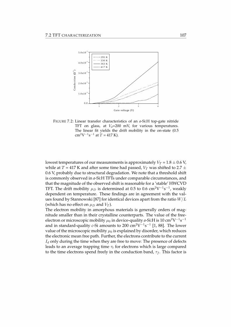
7.2 TFT CHARACTERIZATION 107
1 2 3 4
0.0
1.0x10⁻⁵
2.0x10⁻⁵
3.0x10⁻⁵
4.0x10⁻⁵
5.0x10⁻⁵
295 K 330 K 363 K 417 K
Con
du
ctio
n (
Ω-1)
Gate voltage (V)
FIGURE 7.2: Linear transfer characteristics of an a-Si:H top-gate nitrideTFT on glass, at Vd=200 mV, for various temperatures.The linear fit yields the drift mobility in the on-state (0.5cm2V−1s−1 at T = 417 K).
lowest temperatures of our measurements is approximately VT = 1.8 ± 0.6 V,while at T = 417 K and after some time had passed, VT was shifted to 2.7 ±0.6 V, probably due to structural degradation. We note that a threshold shiftis commonly observed in a-Si:H TFTs under comparable circumstances, andthat the magnitude of the observed shift is reasonable for a ’stable’ HWCVDTFT. The drift mobility µD is determined at 0.5 to 0.6 cm2V−1s−1, weaklydependent on temperature. These findings are in agreement with the val-ues found by Stannowski [87] for identical devices apart from the ratio W/L(which has no effect on µD and VT ).The electron mobility in amorphous materials is generally orders of mag-nitude smaller than in their crystalline counterparts. The value of the free-electron or microscopic mobility µ0 in device-quality a-Si:H is 10 cm2V−1s−1
and in standard-quality c-Si amounts to 200 cm2V−1s−1 [1, 88]. The lowervalue of the microscopic mobility µ0 is explained by disorder, which reducesthe electronic mean free path. Further, the electrons contribute to the currentId only during the time when they are free to move: The presence of defectsleads to an average trapping time τt for electrons which is large comparedto the time electrons spend freely in the conduction band, τf . This factor is

108 DIFFUSION NOISE IN TFTS
contained in the drift mobility µD quite straightforwardly,
µD =τf
τf + τtµ0. (7.3)
Taking the usual value for µ0 = 10 cm2V−1s−1 in device-quality a-Si:H, thefraction of the time an electron spends freely appears to be 0.05 for the TFTin the on-state.
7.3 Noise measurements
Noise spectra were measured using the setup described in section 2.3. Alarge series resistance was connected to the device in order to keep the draincurrent Id supplied by the battery virtually constant. The gate voltage wasprovided by an additional battery. In the Ohmic regime we find SVd
(f)/Vd2
to be independent of Vd in our TFT. Given the constant current, we haveSVd
(f)/Vd2 = SG(f)/G2, where G is the device conductance [15]. We can
conclude that we deal with conductance fluctuations. Noise experimentswere performed at a voltage Vd = 200 mV where the TFT is Ohmic. Thespectra resulted from averaging over 300 individual spectra.
7.3.1 Noise in the above-threshold regime
In the above-threshold regime of the TFT (see Fig. 7.3) the usual 1/f noise-component is observed [72, 73, 74, 75, 76, 77]. That component of the noiseappears to scale with 1/N (Hooge’s law [80]), where N is the number ofelectrons, which can be derived from conductivity data. With decreasingN , however, a 1/f1/2-contribution gradually takes over the 1/f noise. Theanalysis of low-frequency noise data in the off-state is virtually impossibledue to the high device resistance (> 3 MΩ). Owing to the large W/L ratio ofour device, the range in the near- and below-threshold regime accessible fornoise measurements is large enough before the off-state is reached, enablingus to carry out a detailed analysis.
7.3.2 Noise spectra in the sub-threshold regime
In Fig. 7.4 a typical noise spectrum of a TFT near threshold is plotted. Thisspectrum was measured at T = 417 K and just at the threshold voltage. Char-acteristic for the noise spectra near and below threshold and at temperaturesin the range from 295 K to 417 K is a power law with a slope of -1/2 at low

7.4 1D DIFFUSION NOISE 109
100
101
102
103
10-15
10-14
10-13
10-12
10-11
1/f
1/f 1/2
Frequency f (Hz)
SV
/V
2 (
Hz-1
)
VT = 2.7 V
VG = V
T +
0.0 V 1.0 V 3.5 V
FIGURE 7.3: Illustration of two noise mechanisms effective just abovethreshold (at VG=VT +1.0 V). In the ’on-state’ of the transis-tor, 1/f noise rules, whereas near threshold a f−1/2 spectralcomponent shows up, indicative of diffusion noise. Measure-ments at Vd = 200 mV and at T = 417 K.
frequencies. Another feature is the ’kink’ from the -1/2- slope to a slope of-3/2 in the high-frequency range. The kink in this spectrum is at a frequencyfkink = 260 ± 40 Hz. The noise spectrum is quantitatively accounted for bydiffusion theory, which is explained in the next section.
7.4 1D Diffusion noise
7.4.1 1D diffusion noise theory
The problem of one-dimensional diffusion noise was treated by MacFarlaneand Burgess, while in two and three dimensions the problem was solved byVan Vliet and Fassett (for an overview see Ref. [17]). The problem can besolved by Green’s function theory (see Chapter 3). Although our problem isin principle two-dimensional, with electrons diffusing across the length andwidth of the channel, the large W/L ratio of 950 reduces the problem to onlyone dimension: In 2D one would expect two spectral kinks correspondingto W and L, which should then be 9502 ≈ 106 Hz apart from each other(see Eq. 7.6), and can not both be observed in our experimentally accessiblefrequency range. The transition to a spectral slope of -3/2 corresponds to thediffusion time on the shortest length scale [89] in the (2D-) system, which isclearly the channel length L. The solution of the diffusion noise equation

110 DIFFUSION NOISE IN TFTS
1 5 10 50 100 500 1000
1. 10 14
5. 10 14
1. 10 13
5. 10 13
1. 10 12
5. 10 12
1. 10 11
Frequency f Hz
esioN
ytisnetniS
V V
2
zH
1
FIGURE 7.4: Typical noise spectrum of a TFT at threshold (VG=2.7 V),Vd=200 mV and T=417 K, where Gexp = 1.25 µΩ−1. Full lineis fitted diffusion noise spectrum, Eq. (7.4), using an effectivediffusion coefficient Deff =0.011 cm2s−1 and N = 1.3·109.
is written in terms of the number N of electrons in a capacitive channel.Applying Poisson statistics ∆N2 = N to the general form of 1D diffusionnoise [17], we obtain
SN (f)N2
=L2
NDeff θ3(1 − e−θ[cosθ + sinθ]), (7.4)
where θ = L(πf/Deff )1/2, Deff is the effective diffusion coefficient and Lthe channel length. The solution can be separated into two spectral regions[15]:
SN (f)N2
=L
N√
πfDeff, (f−1/2 branch)
=√
Deff
NL(πf)3/2. (f−3/2 branch) (7.5)
7.4.2 Fits to the spectral kink
The transition between the two branches leads to a kink in the spectrum ata frequency
fkink =Deff
πL2. (7.6)

7.4 1D DIFFUSION NOISE 111
As mentioned above, the effective diffusion coefficient is the relevant pa-rameter here taking due account of the fact that only a fraction of the carriersis mobile, (c.f. the drift mobility in Eq. (7.3)). In Fig. 7.4 the exact theoreticalsolution, Eq. (7.4), was applied to fit to the data, with the values of N andDeff as fitting parameters, and with the channel length L fixed to 50 µm.The spectral form of the exact solution tracks the 417 K-data (see Fig. 7.4)satisfactorily for a value of N and of Deff listed in Table 7.2. In the next sec-
Gexp(µΩ−1) Gkink(µΩ−1) N (dim.less) Deff (cm2s−1)1.25 2.56 (1.3 ± 0.2) · 109 0.011 ± 0.0020.64 1.37 (1.1 ± 0.2) · 109 0.007 ± 0.003
TABLE 7.2: Fit results to the noise spectra in the sub-threshold regime ofan a-Si:H TFT held at T = 417 K and operated at 200 mV drainbias voltage, using Eq. (7.4). Using the fit results, the conduc-tion Gkink is calculated from Eq. (7.9).
tion we will see that the product NDeff scales with G, resulting in value ofGkink, which turn out to be correspond to the measured values Gexp withina factor of two! We conclude already now that the electrical noise in thenear-threshold region of our TFT is governed by diffusion noise.
7.4.3 Mobility from noise intensity
For most noise spectra we do not find the kink in the accessible spectralrange, but do observe the f−1/2 branch. Therefore, we can determine thevalues for the diffusion coefficient and thus the mobility directly from thenoise intensity. Mobility and diffusion do originate from the same physicalprocess: a random walk with a characteristic mean free path and velocity.For such a process, the Einstein relation is valid, which connects µ0 to D0,the fundamental diffusion coefficient of free carriers. The Einstein relationreads
µD =eDeff
kBT. (7.7)
Next, we use the experimental fact that SV /V 2 is constant. Therefore, therelative number fluctuations SN/N2 equal the relative voltage fluctuationsSV /V 2. The expression for the noise in the f−1/2 branch now reads:
SV (f)V 2
=L√
e
N√
πfkTµD. (7.8)

112 DIFFUSION NOISE IN TFTS
We have two unknown parameters, N and µD, but can also measure G vsgate voltage. The expression for the conductivity σ = NeµD/AL can gener-ally be written in terms of the gate voltage VG as:
N(VG) =G(VG)L2
eµD(VG). (7.9)
We can compute the drift mobility vs gate voltage by eliminating the numberN of electrons (this section), or, vice versa, eliminate µD to compute N (nextsection). Substituting Eq. (7.9) into Eq. (7.8), we obtain for the drift mobility:
µD(SV /V 2, VG) =πfkBT
e3
(LG(VG) SV (f)/V 2
)2. (7.10)
The resulting values of the mobility are plotted as symbols in Fig. 7.5. Thevalues for the diffusion coefficient obtained from the kinks using the Ein-stein relation are included in the plot as open symbols. Alternatively, thedrift mobility was also determined directly from the conduction and plottedas lines in the full range of VG. That alternative approach will be discussedin section 7.4.5. The mobility decreases slightly as the number of electronsin the channel decreases gradually, as expected from the ratio τf/(τf + τt),which also decreases. The transition to a constant mobility level at highgate voltages is in agreement with the general behavior of a transistor in theon-state, Eq. (7.2). The decrease is different for the 417 K-data, since at thetime of the measurements the device had reached a different state by gatestressing, and becomes characterized by a different threshold voltage.
7.4.4 Total number N from noise intensity
The second unknown parameter, which can be extracted from combinednoise and conduction measurements by elimination of the mobility, is thetotal number N of electrons in the channel, which yields
N =e2
πfkBTG(SV /V 2)2. (7.11)
The resulting value of N is plotted in Fig. 7.6 as symbols. The dependenceon the gate voltage is similar to that of conduction (see Fig. 7.2), as it should.The procedure to obtain N directly from conduction data is based on theprocedure described in section 7.4.5 and results in the four lines in Fig. 7.6,for the four temperatures.

7.4 1D DIFFUSION NOISE 113
1 2 3 40.01
0.1
295 K 330 K 363 K 417 K kink 417 KM
obilit
y µ D
(cm
2s-1
V-1)
Gate voltage (V)
FIGURE 7.5: Drift mobility determined in three ways; from the kink (opensymbols), from the combination of measured noise intensityand conduction (filled symbols), and from the measured con-duction only (lines).
1 2 3 40.0
2.0x10⁹
4.0x10⁹
6.0x10⁹
8.0x10⁹
1.0x10¹⁰
1.2x10¹⁰
1.4x10¹⁰
295 K 330 K 363 K 417 K
Tota
l n
um
ber
N o
f el
ectr
on
s
Gate voltage (V)
FIGURE 7.6: Total number N of electrons vs gate voltage. Combined noiseintensity and conduction produce the data points, lines wereobtained from measured conduction.

114 DIFFUSION NOISE IN TFTS
7.4.5 Mobility and N directly computed from the conduction only
In the sub-threshold regime, the current is strongly suppressed (approxi-mately by a factor of 25, see left-hand side of the curve in Fig. 7.2). As amatter of fact, the physics of the sub-threshold regime is very complicated,because the electron concentration nearly vanishes in the channel. We con-sider the effects on the various parts of the expression for the current, Eq.(7.2). First, according to Eq. (7.3) a reduction in the number of free carriersresults is a lower value of the drift mobility, because τf is reduced by trap-ping. Second, the capacitance Ci may decrease with decreasing VG, becausethe average distance di at which electrons in the channel are separated fromthe gate contact increases. At high gate voltages, the insulator thickness lim-its the separation to 300 nm. At low gate voltages the average distance mayrise, but no more than 400 nm, resulting in a decrease of the capacitance bya factor of two at maximum (due to the inverse propotionality of Ci to di).This is not sufficient to explain the full suppression of the current. Third,the width W and length L could change, but we consider these effects to benegligible.From the above considerations, only the mobility is expected to vary withgate voltage. Then, we apply the current-voltage relation for the transistor,Eq. (7.2) to the sub-threshold regime, compute dG/dVG (see Fig. 7.2), andderive
dG
dVG= Ci
W
LµD(G) + Ci
W
L
dµD(G)dVG
(VG − VT ). (7.12)
In the on-state this gives dG/dVG = CiWL µD, as it should be. In order to
determine the drift mobility µD, we take the second derivative d2G/dV 2G.
Neglecting the third order term, we have d2G/dV 2G ≈ 2 Ci
WL dµD/dVG. Sub-
stitution in Eq. (7.12) gives for the drift mobility
µD(G) ≈ L
CiW
dG
dVG− 1
2L
CiW
d2G
dV 2G
(VG − VT ). (7.13)
This result allows us to experimentally determine the variation of the ratioτf/(τf + τt) as a function of gate voltage (cf. Eq. (7.3)).This approach works well, regarding the correspondence with the mobilityvalue from the noise data in Fig. 7.5 and with N in Fig. 7.6. Apparently,keeping the derivatives of the conduction up to the second order is suffi-cient for a realistic determination of N and µD. Despite the complex physicsof the sub-threshold regime, our calibration with the diffusion noise data

7.5 DISCUSSION 115
shows that the standard current-voltage relationship Eq. (7.2) with a vary-ing mobility Eq. (7.13) holds satisfactorily.
7.5 Discussion
7.5.1 Diffusion noise phenomenon
Well documented examples of diffusion noise are rare. In semiconductorliterature only a few examples of diffusion noise are reported [15]. The rea-son is that relaxation of carriers is generally dominated by other processessuch as drift, generation and recombination or 1/f noise. Indeed, the noisespectra in Fig. 7.3 show a transition from diffusion dominated noise to 1/fnoise when the gate voltage is increased. We do observe the usual 1/f noisein the on-state of the a-Si:H transistor [72, 74, 77]. Owing to the lithographicfabrication of a contact pattern which sets the W/L ratio to 950, large cur-rents could flow which enabled noise measurements in the sub-thresholdregime of TFTs. Consistent with Hooge’s law, the 1/f noise observed in theabove-threshold regime is proportional to 1/N , like diffusion noise. Fromthis we may conclude that the transition from 1/f noise into diffusion noisewhen the gate voltage is decreased, is caused by the decrease of µD in thesub-threshold regime characteristic for amorphous semiconductors.
7.5.2 Mobility values
When we compare the value of the drift mobility µD ≈ 0.3 cm2V−1s−1 (forT=295, 330 and 363 K) with the estimate for the microscopic mobility µ0 ina-Si:H of 10 cm2V−1s−1 [1], we arrive at τf/(τt + τf ) of 0.03. For the datasetsmeasured at 295, 330 and 363 K, the values of Deff found are around 0.01cm2s−1 (see Fig. 7.5), which would lead to a kink around 130 Hz. Unfortu-nately, a kink around that frequency can not be observed due to suppressionof the noise by the RC-time of the detection system, which is in the samerange.The 417 K-data are found to have smaller values of the mobility, due toa smaller values of τf/(τt + τf ), which was confirmed independently bydirect determination of the mobility from conduction measurements only.Also, the dependence on VG is stronger for the 417 K-data. The explanationfor the quantitative differences with the data measured at 295, 330 and 363K is the threshold shift due to gate stressing before the 417 K-data set wasmeasured.

116 DIFFUSION NOISE IN TFTS
We have found that the direct determination of both µD and N using con-duction measurements only results in values which are for the larger partwithin the error of values from the combination of noise intensity and con-duction. Therefore we propose Eq. (7.13) as a quick approach to determinethe mobility in the near- and sub-threshold regime.
7.6 Conclusion and outlook
We find in an a-Si:H TFT operated in the sub-threshold range, that the 1/fnoise becomes buried under 1D diffusion noise, because the drift mobilitydecreases. Theoretical 1D diffusion noise spectra in that regime fit well tothe measured spectra, and explain the observed f−1/2 branch in the low-frequency region of the spectrum. Combined noise and conduction mea-surements enable to separate and determine in the sub-threshold regimeboth the number of electrons N and the drift mobility µD ≈ 0.3 cm2V−1s−1.A decrease of the gate voltage in the sub-threshold regime leads obviouslyto a decrease of the number of electrons, and further to the a decrease in theratio τf/(τt+τf ), observed as a decrease of µD. The calculated ratio betweenµD and µ0 is consistent with the results from conduction measurements onlyand with the literature value of the microscopic mobility µ0=10 cm2V−1s−1.The noise spectra in the sub-threshold regime can consistently and quanti-tatively be described by 1D diffusion noise. Noise measurements enable theseparate determination of the number of electrons in the channel and thedrift mobility. Especially in the sub-threshold regime, where the conduc-tion deviates from the usual behavior, this leads to valuable results. It turnsout that application of the standard current-voltage relation for a field-effecttransistor with a mobility that is allowed to vary is in agreement with aprocedure using combined noise and conduction measurements. We finallyremark that the noise spectra after a small (1V) threshold shift still satisfy1D diffusion noise spectra.It would be interesting to carry out noise measurements in the sub-thresholdregime of polycrystalline Si TFTs, to investigate the contribution of diffusionnoise in relation to other kinds of noise. The W/L ratio of the TFTs shouldexceed 500 to be able to measure noise in the sub-threshold regime. An-other interesting suggestion is to carry out measurements on a TFT with atwo-dimensional channel, which should result in a spectrum which is dev-ided in three regions of different spectral slopes [89].

References
[1] R. Street, Hydrogenated amorphous silicon, Cambridge University Press,Cambridge, 1991.
[2] N. Mott and E. Davis, Electronic Processes in Non-crystalline Materials,Clarendon Press, Oxford, 2 edition, 1979.
[3] N. Ashcroft and N. Mermin, Solid state physics, Hartcourt Brace CollegePubl., New York, 1976.
[4] P. Thomas and H. Overhof, Properties and Applications of AmorphousMaterials, pages 261–290, NATO Science Series, Kluwer, 2001.
[5] J. van Hapert, PhD thesis, Utrecht University, 2002.
[6] D. Staebler and C. Wronski, Appl. Phys. Lett 31, 292 (1977).
[7] M. Powell, S. Deane, and R. Wehrspohn, Phys. Rev. B 66, 155212 (2002).
[8] H. Branz, Phys. Rev. B 59, 5498 (1999).
[9] S. Deane, R. Wehrspohn, and M. Powell, Phys. Rev. B 58, 12625 (1998).
[10] R. Wehrspohn, S. Deane, I. French, and M. Powell, J. Non-Cryst. Solids266-269, 49 (2000).
[11] G. Munyeme, PhD thesis, Utrecht University, 2003.
[12] M. Stutzmann, M. Brandt, and M. Bayerl, J. Non-Cryst. Solids 266-269,1 (2000).
[13] M. Powell and S. Deane, Phys. Rev. B 48, 10815 (1993).
[14] M. Powell and S. Deane, Phys. Rev. B 53, 10121 (1996).
117

118 REFERENCES
[15] A. van der Ziel, Noise in Solid State Devices and Circuits, Wiley and Sons,New York, 1986.
[16] M. Kirton and M. Uren, Adv. Phys. 38, 367 (1989).
[17] K. van Vliet and J. Fassett, Fluctuation Phenomena in Solids, ed. R.E.Burgess, chapter 7, Academic Press, New York, 1965.
[18] P. Dutta, P. Dimon, and P. Horn, Phys. Rev. Lett. 43, 646 (1979).
[19] K. Lee, K. Amberiadis, and A. van der Ziel, Solid State Electronics 25,999 (1982).
[20] F. Hooge, IEEE Trans. Electron Dev. 41, 1926 (1994).
[21] P. Dutta and P. Horn, Rev. Mod. Phys. 53, 497 (1981).
[22] D. Quicker and J. Kakalios, Phys. Rev. B 60, 2449 (1999).
[23] J. Belich and J. Kakalios, Phys. Rev. B 66, 195212 (2002).
[24] J. Belich and J. Kakalios, to be published, SPIE Conf. Proc.
[25] L. Lust and J. Kakalios, Phys. Rev. Lett. 75, 2192 (1995).
[26] H. Overhof and W. Beyer, Philos. Mag. B 43, 433 (1981).
[27] J. Fan and J. Kakalios, Phys. Rev. B 47, 10903 (1993).
[28] D. Quicker, P. West, and J. Kakalios, Mat. Res. Soc. Proc. 467, 73 (1997).
[29] C. Parman and J. Kakalios, Phys. Rev. Lett. 67, 2529 (1991).
[30] P. Verleg, PhD thesis, Utrecht University, 1997.
[31] G. Snyder, M. Weissman, and H. Hardner, Phys. Rev. B 56, 9205 (1997).
[32] M. Gunes, R. Johanson, and S. Kasap, Phys. Rev. B 60, 1477 (1999).
[33] R. Johanson, D. Scansen, and S. Kasap, J. Vac. Sci. Technol. B 17, 73(1999).
[34] R. Johanson, S. Kasap, F. Gaspari, D. Yeghikyan, and S. Zukotynski, J.Vac. Sci. Technol. A 18, 661 (2000).

REFERENCES 119
[35] M. Gunes, R. Johanson, S. Kasap, J. Yang, and S. Guha, J. Non-Cryst.Sol. 299-302, 425 (2002).
[36] S. Kasap et al., J. Mat. Sc., in press, 2003.
[37] E. Ullersma, PhD thesis, Utrecht University, 1998.
[38] A. D’Amico, G. Fortunato, and C. van Vliet, J. Non-Cryst. Solids 77-78,499 (1985).
[39] M. Bacoicchi, A. D’Amico, and C. van Vliet, Solid-St. Electron. 34, 1439(1991).
[40] F. Bathaei and J. Anderson, Phil. Mag. B 55, 87 (1987).
[41] P. Verleg and J. Dijkhuis, Phys.Rev. B 58, 3904 (1998).
[42] P. Verleg and J. Dijkhuis, Phys. Rev. B 58, 3917 (1998).
[43] S. Reynolds, C. Main, and M. Rose, J. Non-Cryst. Solids 227-230, 233(1998).
[44] C. Main, S. Reynolds, and R. Badran, Mat. Res. Soc. Symp. Proc. 715,A2.2 (2003).
[45] S. Kasap, 2003, personal communication.
[46] R. Schropp, personal communication.
[47] R. Schropp and M. Zeman, Amorphous and microcrystalline silicon solarcells; modeling, materials and device technology, Kluwer, Boston, 1998.
[48] S. Fonash, A manual for AMPS-1D for Windows 5/NT; a one-dimensionaldevice simulation program for the analysis of microelectronic and pho-tonic structures, Pennsylvania State University, 1997, see alsohttp://www.psu.edu/dept/AMPS.
[49] P. McElheny, J. Arch, H. Lin, and S. Fonash, J. Appl. Phys. 64, 1254(1988).
[50] M. Zeman, M. Kroon, and J. van den Heuvel, Amorphous SemiconductorAnalysis (ASA), Delft Univerity of Technology, Delft, the Netherlands,user manual version 3.0 edition, 1999.
[51] M. van Veghel, Master’s thesis, Utrecht University, 1999.

120 REFERENCES
[52] M. von der Linden, PhD thesis, Utrecht University, 1994.
[53] C. van Vliet, J. Appl. Phys. 93, 6068 (2003).
[54] C. van Vliet, IEEE Transactions 41, 1902 (1994).
[55] A. van der Ziel, Solid State Physical Electronics, Prentice-Hall, 3rd edi-tion, 1976.
[56] J. Fassett, Electronic fluctuations in solids involving thr transport, genera-tion, and recombination of charge carriers, PhD thesis, Univ. Minnesota,Minneapolis, USA, 1962.
[57] J. Bakker, P. van Capel, B. Fine, and J. Dijkhuis, Mat. Res. Soc. Symp.Proc. 715, A2.6 (2003).
[58] B. Shklovskii and A. Efros, Electronic properties of doped semiconductors,volume 45 of Springer Ser. Solid-State Sciences, Springer, Heidelberg,1984.
[59] V. Arkhipov and G. Adriaenssens, Phil. Mag. B 76, 11 (1997).
[60] V. Arkhipov and G. Adriaenssens, Phys. Rev. B 54, 16696 (1996).
[61] F. Zhong and J. Cohen, Phys. Rev. Lett. 71, 597 (1993).
[62] P. Anderson, Phys. Rev. 109, 1492 (1958).
[63] B. Fine, J. Bakker, and J. Dijkhuis, Accepted for publication in Phys.Rev. B (2003).
[64] A. van Rheenen, G. Bosman, and R. Zijlstra, Solid-St. Electron. 30, 259(1987).
[65] G. Khera and J. Kakalios, J. Appl. Phys. 56, 1918 (1997).
[66] D. Adler and E. Yoffa, Phys. Rev. Lett. 36, 1197 (1976).
[67] J. Wei, M. Sun, and S. Lee, Appl. Phys. Lett. 71, 1498 (1997).
[68] R. Weisfield, J. Appl. Phys. 59, 6401 (1982).
[69] V. Cech, Solid-state Electronics 41, 81 (1997).
[70] W. O’Mara, Liquid crystal flat panal displays: manufacturing, science andtechnology, Van Nostrand Reinhold, New York, 1.ed. edition, 1993.

REFERENCES 121
[71] J. Xu, P. Lai, and Y. Cheng, J. Appl. Phys. 86, 5203 (1999).
[72] M. Valenza et al., J.Appl.Phys. 79, 923 (1996).
[73] J. Rhayem, M. Valenza, D. Rigaud, N. Szydlo, and H. Lebrun, J. Appl.Phys. 83, 3660 (1998).
[74] J. Rhayem, D. Rigaud, M. Valenza, N. Szydlo, and H. Lebrun, J. Appl.Phys. 87, 1983 (2000).
[75] C. Dimitriadis, J. Brini, G. Kamarinos, V. Gueorguiev, and T. Ivanov, J.Appl. Phys. 83, 1469 (1998).
[76] C. Angelis et al., Appl. Phys. Lett. 74, 3684 (1999).
[77] J. Boudry and L. Antonuk, J. Appl. Phys. 76, 2529 (1994).
[78] M. Deen, S. Rumyantsev, and J. Orchard-Webb, J. Vac. Sci. Technol. B16, 1881 (1998).
[79] L. Vandamme, R. Feyaerts, G. Trefan, and C. Detcheverry, J. Appl. Phys.91, 719 (2002).
[80] F. Hooge, Phys. Lett. A. 29, 139 (1969).
[81] K. Hung, P. Ko, C. Hu, and Y. Cheng, IEEE Trans. Electron DevicesED-37, 654 (1999).
[82] G. Ghibaudo, O. Roux, C. Nguyen Duc, F. Balestra, and J. Brini, Phys.Status Solidi A 124, 571 (1991).
[83] D. Cobden and B. Muzykantskii, Phys. Rev. Lett. 75, 4274 (1995).
[84] R. Keijsers, O. Shklyarevskii, and H. van Kempen, Phys. Rev. Lett. 77,3411 (1996).
[85] M. Peters, J. Dijkhuis, and L. Molenkamp, J. Appl. Phys. 86, 1523 (1999).
[86] B. Stannowski and R. Schropp, Thin Solid Films 383, 125 (2001).
[87] B. Stannowski, PhD thesis, Utrecht University, 2002.
[88] S. Sze, Physics of semiconductor devices, John Wiley and Sons, New York,2nd edition, 1981.
[89] R. Voss and J. Clarke, Phys. Rev. B 13, 556 (1976).


Summary
Noise measurements on two classes of semiconductor devices are reportedin this thesis: on solar-cell devices and thin-film transistors. The aim is toprovide a quantitative description of the experiments. The first class ofdevices displays one of the most intruiging physical phenomena in semi-conductors: 1/f noise. The term refers to resistance fluctuations with a1/f frequency dependence of the noise intensity. This kind of noise is re-ported in many different systems but lacks a universal explanation. Hydro-genated amorphous silicon (a-Si:H) is an example of a semiconductor whichis known to exhibit a large degree of disorder, and, as a result, a large vari-ation in microscopic energy barriers, that govern capture and emission ofcharge carriers. Two mechanisms to explain the observed 1/f resistancenoise in a-Si:H devices are investigated: generation-recombination noiseand potential fluctuations at defects. The latter mechanism appears to yielda quantitative prediction of the noise spectra.We study the electronic properties of hydrogenated amorphous silicon. Thismaterial finds an application in the two studied classes of devices: solarcells and thin-film transistors (TFTs). These devices have the unfortunateproperty to degrade upon prolonged light-soaking and gate bias stressing,respectively. In order to study the properties of undoped a-Si:H, relevantfor solar cells, an intrinsic layer is sandwiched between thin doped layers,resulting in nin and pip device structures. Chapter 2 of this thesis deals withcurrent density - voltage (J-V ) characteristics, which are nearly Ohmic atlow voltages (<0.15 V) and gradually become superlinear at high voltagesdue to the presence of space charge. A simulation program takes band bend-ing into account and was applied to fit J-V characteristics measured at dif-ferent temperatures simultaneously. As a result, the defect density, the en-ergy position, and width of the Gaussian distributions of deep defects areobtained. These material parameters are used as input parameters in twoquantitative theories to describe the observed noise in nin devices.
123

124 SUMMARY
The first mechanism, generation-recombination (g-r) noise, is addressed inChapter 3. G-r noise originates from local emission and capture events be-tween traps and the conduction band (in case electrons are the majoritycarriers). Using Green’s function theory, g-r noise is calculated for a one-dimensional semiconductor device with traps, taking due account of carriertransport. Although capture and emission times are in the right (ms) range,the calculated noise intensity turns out to be five to six orders of magni-tude below the measured noise level and thus is negligible. Clearly, anothernoise source must cause the 1/f noise in a-Si:H. The observations turn outto be explained very well by a microscopic mechanism treated in Chapter4. The timescale of the fluctuations is again the capture or emission time fordeep defects. But now it is used, when an electron is emitted or captured,that the charge state of a deep defect fluctuates. As a result, the potentialaround that defect will fluctuate, depending on the degree of screening bysurrounding defects and the contacts. Free electrons will instantaneouslyadjust to the fluctuating local potential. That adjustment causes a carriernumber fluctuation, which is measured as a voltage fluctuation in presenceof a constant current. Our theory treats fluctuations of charged deep defectsin the presence of screening by surrounding defects and the contacts usingthe equilibrium description of defects. Since there is only a small number of(randomly located) deep defects which is able to change their charge state,the potential landscape exhibits long-range fluctuations.The theory predicts the noise intensity accurately, without any adjustableparameters. The shape of the noise spectrum is fitted by two parameters ofthe potential landscape. The complete temperature dependence of the noisespectra is consistently described by a Gaussian distribution of potential bar-riers, located 0.27 ± 0.05 eV above the conduction band edge, and with ahalfwidth of 0.09 ± 0.02 eV. These material parameters, obtained with noisespectroscopy, cannot be obtained from other (electrical) measurement tech-niques. In Chapter 5 experiments on different devices are explained by thetheory of long-range potential fluctutations. The area and thickness depen-dence is examined, the absence of an isotope effect is demonstrated and pipdevices are studied, where holes are the majority carriers. The comparisonof the results obtained from the pip and nin devices demonstrates the ex-istence of a universal distribution of emission barriers in a-Si:H/D for thecarrier escape from deep defects.In Chapter 6 the relation between degradation and noise is studied in nindevices. Additional conductivity measurements are analyzed to determinethe defect density before and after degradation. After degradation, the cur-

SUMMARY 125
vature of noise spectra is unaffected, while the intensity increases by a smallfactor. These observations are consistent with the theoretical predictions us-ing the measured increase of the defect density. The potential landscapedoes not seem to change significantly upon degradation, as judged fromthe constant shape of the spectra. The theory of long-range potential fluc-tuations successfully and quantitatively predict the 1/f noise spectra in ourfilms of a-Si:H and most likely in other materials with regions of poor screen-ing.Noise measurements on a-Si:H TFTs are described in Chapter 7. Earlierexperiments revealed 1/f noise which satisfied Hooge’s empirical law inthe on-state of the transistor. We were able to measure noise in the sub-threshold regime of the transistor. At the threshold voltage and below, diffu-sion noise dominates over 1/f noise. Diffusion of electrons through the one-dimensional channel is identified as the source of the noise. The number offree electrons as determined from combined noise and conduction measure-ments is in quantitative agreement with the usual approximation from con-duction measurements only. As expected, the drift mobility extracted fromthe combined noise and conduction data varies with the conditions of thechannel, and amounts to 0.3 cm2V−1s−1 near threshold.


Samenvatting voorniet-vakgenoten
’Morfografisch amorf,’ mompelde professor Prlwytzkofski al schrij-vend. ’Der fenomeen is niet uit kristallijnen opgebouwd en kandeswegen niet existeren. Toont echter ener buitenordentelijk ac-comodatievermogen, dat nader studeerd worden moet.’- De Kon Gruwer, Marten Toonder (1971)
In dit proefschrift staan elektrische fluctuatiemetingen aan een ingewikkeldmateriaal centraal. Het gaat om de halfgeleider amorf silicium waarin wa-terstof is opgenomen. Het is een wanordelijk materiaal, in tegenstellingtot kristallijn silicium, waar de silicium atomen netjes gerangschikt zijn. Inamorf silicium bevinden de atomen zich op verschillende afstanden van el-kaar. Er bestaan ook plaatsen waar zelfs geen bindingen tussen de siliciumatomen bestaan. Op die plaatsen blijven bungelende bindingen over, die’defecten’ worden genoemd. Het proces waarbij door externe factoren, zoalssterke en langdurige belichting, het aantal defecten in een monster vergrootwordt, heet degradatie. Een halfgeleider kan licht absorberen, waarbij zo-wel positieve als negatieve lading vrijgemaakt wordt. Dit principe is toege-past in een zonnecel, waarin vrijgemaakte deeltjes met tegengestelde ladingvan elkaar gescheiden worden hetgeen tot een elektrische spanning leidt.Een andere belangrijke toepassing van amorf silicium is de dunne laag tran-sistor of TFT structuur, wel gebruikt in flat-pannel displays. Een transistor isniets anders dan een elektonische schakelaar. Ook al zijn er technologischeverbeteringen denkbaar in de genoemde bestaande gelaagde structuren ofdevices, toch is deze studie er niet op gericht om daarvoor praktische oplos-singen aan te dragen. Het doel van dit werk is om fluctuaties kwantitatiefte meten en te beschrijven. Zodoende kan meer vat gekregen worden ophet complexe, wanordelijke materiaal en de gevolgen van degradatie op de
127

128 SAMENVATTING
eigenschappen van het materiaal. Er worden twee meetmethoden en di-verse analysemethoden uit de kast gehaald. In meerdere gevallen moesteen bestaande theorie worden toegepast op de omstandigheden van de de-vices. In een geval werd een complete theorie van de grond af aan opge-bouwd. Ter ondersteuning van de ruismetingen, die centraal staan in ditproefschrift, dienen metingen van de elektrische geleiding. Met geleidings-metingen in een groot temperatuurbereik kan het aantal geleidingselektro-nen in het monster worden gemeten, alsmede de gemiddelde energie beno-digd voor thermische overbrugging van de barriere voor geleiding.De eigenlijke fenomenen waarvan studie gemaakt is, zijn de weerstands-fluctuaties. Elektrische fluctuaties worden gemeten als ruis in de spanningin een variant van de zonnecel en in een transistor. Het ruissignaal wordtversterkt en omgezet naar de frequentie componenten die er in zitten. Ditruisspectrum geeft precies weer hoe sterk het materiaal ruist bij bepaaldefrequenties. In de praktijk gaat het om zwakke signalen, waarin vaak mi-croscopische verschijnselen verborgen zijn. Het is de uitdaging om de inten-siteit en de vorm van de gemeten ruisspectra te kunnen begrijpen. De eerdergenoemde geleidingsmetingen zijn daarbij handig, omdat ze dezelfde toe-stand karakteriseren waaronder ruismetingen worden verricht. Geleidings-en ruismetingen hangen echter op een andere manier af van de elektrischeeigenschappen van het materiaal. Door de meetgegevens te combinerenkan een completer beeld van de elektrische eigenschappen van het materi-aal verkregen worden.In Hoofdstuk 2 staat beschreven hoe een simulatieprogramma gebruikt isom een deel van de elektrische eigenschappen van een device te achterha-len. Op deze manier kan de verdeling van bungelende bindingen gekarak-teriseerd worden. Zoals gezegd zijn deze defecten plekken in het netwerk,waar silicium niet gebonden is aan een ander silicium atoom of waterstof.Dergelijke defecten leveren geladen toestanden op in het materiaal, waar be-wegende lading op terecht kan komen (vangst) en van waaruit lading kanontsnappen (emissie). Deze processen vormen de basis van twee verschil-lende theorieen.Het ruistype waar lokale vangst- en emissie processen leiden tot fluctua-ties aan de contacten, wordt generatie-recombinatie ruis genoemd (Hoofd-stuk 3). De intensiteit van dit type ruis blijkt ver beneden het waargenomenniveau van 1/f ruis uit te komen. Er moet dus een andere oorzaak voorhet fenomeen zijn. Die oorzaak is gevonden in de fluctuaties van de lokaleelektrische potentiaal, ten gevolge van ladingsveranderingen van defecten,op de tijdschaal van dezelfde vangst- en emissieprocessen. Die processen

SAMENVATTING 129
worden gekarakteriseerd door het energieverschil tussen het defect en delocale barriere voor emissie. De sterkte van deze potentiaalfluctuaties hangtaf van de afscherming van lading door naburige defecten (Hoofdstuk 4).Zowel de fluctuatiefrequenties als de ruisintensiteit blijken goed overeen tekomen met de metingen. Metingen in het gehele temperatuurbereik kunnenbeschreven worden met behulp van een verdeling van potentiaal barrieres.Daarmee komen we op een essentieel ingredient van de nieuwe theorie: datde willekeurige ordening van de atomen leidt tot een landschap van poten-tiaalbergen en -dalen. Met ruismetingen is het mogelijk om dit landschapte beschrijven - wat onmogelijk is voor geleidingsmetingen, die slechts voorde dalen (de geleidingsband) gevoelig zijn. Een reeks experimentele resul-taten, beschreven in Hoofdstuk 5, ondersteunt deze theorie. Zo wordende effecten ten gevolge van een andere laagdikte goed voorspeld, en is ergeen afhankelijkheid van het gebruikte isotoop van waterstof. Anders ge-zegd, gebruik van zwaar waterstof in plaats van het gebruikelijke waterstofhad geen invloed op de ruismetingen. Uit een experiment met positieve la-dingsdragers blijkt dat het potentiaallandschap er vrijwel hetzelfde uitzietals het landschap voor elektronen. Het degradatie experiment, beschrevenin Hoofdstuk 6, laat zien dat bij een geringe toename van de aantallen de-fecten de ruisintensiteit nauwelijks toeneemt en qua vorm gelijk blijft. Delichte stijging is in overeenstemming met de theorie. De ongewijzigde vormvan het spectrum zou erop kunnen duiden dat het potentiaallandschap nietessentieel verandert in de aanwezigheid van meer defecten. Met de theorievan potentiaalfluctuaties is een bevredigende verklaring gevonden voor deruismetingen aan amorf silicium. Omdat het beschreven mechanisme ge-baseerd is op algemene natuurkundige beginselen, is het waarschijnlijk dathet ook in andere (halfgeleider) systemen op zal treden. En dan met namein die gebieden, waar een zwakke mate van afscherming bestaat, net als inhet bestudeerde materiaal. Ruismetingen bevatten dus unieke informatieover het potentiaal landschap, dat ongevoelig voor degradatie lijkt te zijn.Daarmee is aanvullende experimentele informatie gewonnen in een belang-rijk onderzoeksveld.Naast bovenstaand onderzoek werden ruismetingen uitgevoerd aan dunnelaag transistoren bestaand uit amorf silicium (Hoofdstuk 7). Transistorenzijn elektronische schakelaars, die met behulp van een spanning de zoge-naamde ’gate’ (hek) geschakeld worden. Het is bekend dat dit type tran-sistor 1/f ruis produceert in de situatie dat het hek open staat. We heb-ben met name metingen gedaan in de buurt van de drempelspanning, alser een kleine stroom door het geleidende kanaal loopt. In die toestand

130 SAMENVATTING
blijken elektronen aanleiding te geven tot fluctuaties zodra ze het kanaalovergestoken zijn volgens de gang van een dronken man. Dit zogenaam-de ’diffusief transport’ in de lengterichting van het kanaal bepaalt dus hetruisspectrum. De vorm van een diffusie ruisspectrum wordt gekarakteri-seerd door een scherpe overgang tussen twee gebieden met een verschillen-de frequentie-afhankelijkheid. Er is kwantitatieve overeenstemming tussenhet aantal elektronen bepaald uit de geleiding en uit een theoretisch diffusie-ruisspectrum. Daardoor kan de parameter die het gemak aangeeft waarmeeelektronen door het materiaal diffunderen met zekerheid gegeven worden.Dit is de (drift) mobiliteit, en deze bedraagt 0.3 cm2V−1s−1 bij het openenvan de gate (het hek). Deze waarde klopt aardig met de bepaling op grondvan de geleiding, en is bovendien in overeenstemming met de mobiliteit diein het algemeen gevonden wordt. Met ruismetingen kan de mobiliteit - eenmaatgevende grootheid voor de industrie - nu ook bepaald worden in debuurt van de drempelspanning van een transistor.

Dankwoord
Niet alleen het onderwerp, maar zeker ook de samenwerking met anderenvormden voor mij ruim vier jaar lang de motivatie voor dit onderzoek. Aanhet uiteindelijke resultaat hebben velen een belangrijke bijdrage geleverd,waarvoor ik hen graag op deze plaats wil bedanken.Mijn promotor prof. Jaap Dijkhuis dank ik voor zijn goede ideeen, zijn en-thousiasme en zijn durf met betrekking tot het opzetten van grensverleg-gende experimenten. Zijn kritische houding bleek steeds weer waardevol,met name in onze discussies, waarin hij graag de rol van ’advocaat van deduivel’ speelde. Ten slotte wist hij ingewikkelde zaken terug te brengen totde essentie, waar ik veel van opgestoken heb.Voor het inwijden in de ruisspectroscopie dank ik Frans Wollenberg. Metzijn uitgebreide kennis op het gebied van electronica en daarbuiten wist hijvoor al mijn vragen praktische oplossingen aan te dragen. Samen met PaulJurrius zijn prachtige flexibele meetopstellingen tot stand gekomen, waar-voor veel dank aan beide heren. De laatst genoemde ’heer van het goedeleven’ wist op het mechanische en sociale vlak alles soepeltjes te laten ver-lopen.Met de theoretisch onderzoeker dr. Boris Fine deelde ik mijn interesse voor1/f ruis in amorf silicium. Hij wist een theoretische afleiding van meer dan100 formules te produceren die de uiteindelijke verklaring van onze ruisme-tingen bleek te leveren. Boris, bedankt voor je scherpzinnigheid, je precisieen je grote theoretische bekwaamheid. Ook kijk ik terug op een onvergete-lijk Russisch feest bij jou en Ada thuis.Bij prof. Ruud Schropp en dr. Jatin Rath stond de deur altijd open voor vra-gen omtrent amorf silicium. Voor het verzorgen van met name de depositievan het dure ’zwaar waterstof’, amorf silicium, alsmede de gelegenheid deelte nemen aan de werkbesprekingen ben ik hen zeer erkentelijk. De kennis enkunde op het gebied van dunne laag transistoren van dr. Bernd Stannowskizijn van groot belang geweest voor het ruisexperiment aan die transistoren.
131

132 DANKWOORD
De basis voor alle devices werd gelegd door Karine van der Werf, die devele lagen deponeerde, rekening houdend met mijn specifieke wensen.De ruimtevaart-technologen Marcel de Bruin, Nanny Snijder, Ward Haale-bos en Marcel Ridder (SRON, Utrecht) dank ik voor het sputteren van uit-stekende elektrische contacten. Ook mocht ik frequent gebruik maken vande laagdiktemeetfaciliteit. In een verkennend stadium waren Johan Keijzeren Gert Hartman behulpzaam bij het opdampen van contacten. Voor de spe-ciale contactering van de dunne-laag transistoren ben ik dank verschuldigdaan Philips Redhill, GB.De Nederlandse Amerikanen, prof. Van Vliet en prof. Bosman ben ik zeererkentelijk voor hun bezoek in Utrecht en hun waardevolle aanwijzingenmet betrekking tot verschillende ruistheorieen. For interesting discussionsI would like to acknowledge dr. Main, dr. Reynolds, prof. Kakalios, prof.Stutzmann and prof. Adriaenssens. Voor de interesse in mijn werk dank ikprof. Van der Weg en prof. Habraken.Met veel plezier heb ik met de chemici samengewerkt aan een ambitieus ex-periment: ruis in een elektrochemische cel. Aan de chemie met prof. Kelly,prof. Vanmaekelbergh, dr. Erik Bakkers en dr. Marcel di Vece heeft het nietgelegen, evenmin aan de mooie opstelling! Helaas bleken de tijdschalen vande bestudeerde processen in een geval te snel en in een ander geval te traagte zijn.De ervaring en de kennis van mijn jaargenoot Marijn van Veghel op hetgebied van computersimulaties van amorf silicium structuren waren zeerwelkom bij de aanvang van de promotie. Bedankt voor je nuttige adviezen.Ook heb ik veel gehad aan de werkgroep ”opzet en analyse van experimen-ten met behulp van statistische technieken”, mede dankzij de bijdragen vanGijsje Koenderink, Bas Feddes en Elwin de Wolf.Ik heb het altijd heel leuk gevonden om met studenten op onderzoek uit tegaan. Allereerst met Bernard van der Horst, die met succes zijn tanden heeftgezet in een lastig onderwerp: fotogeleiding. Zijn kritische houding en zijntoewijding heb ik zeer gewaardeerd. Met Peter van Capel heb ik op veleonderzoeksterreinen van gedachten gewisseld. Voor zijn inzet, lef en in-zichten ben ik hem dankbaar. Daarnaast hebben we veel lol beleefd aan hetgeexperimenteer op de politieke aandelenmarkt. Timon van Wijngaardenheeft in korte tijd een leuke combinatie van bestaande methoden gemaakt,petje af. Ook bedankt voor jullie gezellige aanwezigheid op de kamer.Voor controle-berekeningen aan het device ben ik Raul Jiminez Zambranoen Geoffrey Munyeme dankbaar. Bij hen kon ik terecht voor gesprekkenover amorf silicium of geheel andere onderwerpen. Arnoud Witt dank ik

DANKWOORD 133
voor het lezen van een gedeelte van mijn proefschrift. Voor waardevollereacties op werkbesprekingen en conferenties zou ik een hele waslijst aanmensen kunnen noemen, maar ik beperk me tot Otto Muskens, Dima Mazu-renko, Marjolein van der Voort, Ruurd Lof en Anke Brockhoff. Gedurendevier jaar in de Debye AiO Commissie heb ik met plezier samengewerkt metTonnis, Marije, Aarnoud, Marieke, Anne, Harm, Gijsje, Claire, Nilesh, Rezaen Didi.Mijn kamergenoten Marjolein van der Voort en later Lennart Karssen ston-den garant voor een prettige werksfeer. Met Clarien Derks kon ik over vanalles en nog wat praten. Die gezelligheid zal ik missen. Een speciale nootvoor al diegenen die zich met grote veerkracht hebben ingezet voor de inter-ne verhuizing, met name Cees de Kok, Paul Jurrius en Gerard van Lingen.De verhuizing bracht ook een geleidelijke verschuiving en verbreding vanhet vakgroepsleven met zich mee. Denkend aan de prettige sfeer van de af-gelopen jaren noem ik met name, en met inbegrip van hen die al eerder ge-noemd werden, de fysici Peter, Michiel, Dries, Erik, Richard, Carolijn en Toi-ne. Verder de chemici Andries, Hans, Stefan, Zeger, Stephen, Paul, Sander,Francois, Harold, Peter, Ageeth en Liesbeth. En ten slotte de colloidfysiciAlfons, Arnoud, Carlos, Didi, Christina en Alexander. Onder lunchtijd hebik samen met andere spelletjes-freaks Tim, Jeroen, Marijn, Beat, Francois,Peter en Pim talloze bordspellen uitgeprobeerd.Mijn familie en vrienden dank ik voor hun interesse in mijn werk. In hetbijzonder dank ik mijn schoonouders voor hun meelevendheid en betrok-kenheid. Ik wil mijn ouders bedanken omdat ze mij hebben gestimuleerd inde richting die ik gegaan ben. Mams, fijn dat je steeds zo betrokken was, endat je echt wilde weten waar ik nu mee bezig was. Paps, bedankt dat je erop belangrijke momenten voor me was.Lieve Mirjam, het was super dat ik jou steeds aan mijn zijde vond in de af-gelopen periode, waarin je geduld aardig op de proef gesteld werd. Het waseen worsteling om in woelige tijden het hoofd boven water te houden, maarhet is ons gelukt!


Curriculum Vitae
De schrijver van dit proefschrift werd op 16 februari 1976 geboren in Oss.Na het behalen van het VWO-diploma (cum laude) op de Christelijke Scho-lengemeenschap Melanchthon te Rotterdam in 1994, begon hij aan de stu-die Natuur- en Sterrenkunde aan de Universiteit Utrecht. In december 1998werd het doctoraalexamen Experimentele Natuurkunde aan de UniversiteitUtrecht met genoegen afgelegd. Het laatste jaar van zijn doctoraalstudiebestond uit een onderzoek naar de oxidatie van ijzer bij de sectie Grens-laagfysica (Universiteit Utrecht) en een stage bij Shell Solar te Helmond.Op 1 januari 1999 trad hij in dienst bij de faculteit Natuur- en Sterrenkun-de van de Universiteit Utrecht als assistent in opleiding bij de sectie ”AtomOptics and Ultrafast Dynamics”van het Debye Instituut. De resultaten vanhet onderzoek zijn beschreven in dit proefschrift en gepresenteerd op eendrietal conferenties: ’the International Conference on Amorphous and Mi-crocrystalline Semiconductors’ (Nice, Frankrijk, 2001 en Campos do Jordao,Brazilie, 2003) en ’Spring Meeting of the Materials Reseach Society’ (SanFransisco, VS, 2002). Tevens werd de zomerschool ’Properties and applica-tions of amorphous materials’ bezocht (Sec, Tjechie, 2001). Naast het onder-zoek begeleidde hij tweedejaars studenten bij het hoofdvak natuurkunde,en was hij actief binnen de Debye AiO Commissie.
135