noise analysis of radiation detector charge …noise analysis of radiation detector charge sensitive...
TRANSCRIPT

Noise Analysis of Radiation Detector Charge Sensitive Amplifier Architectures
T. Noulis a, G. Fikos a, S. Siskos a, G. Sarrabayrouse b,
a Electronics Laboratory of Physics Department, Aristotle University of Thessaloniki, Aristotle University Campus, 54124 Thessaloniki, Greece.
b Laboratoire d’Analyse et d’Architecture des Systèmes LAAS – CNRS, 7 Avenue du colonel Roche, Université de Toulouse, 31077 Toulouse cedex 4, France
Abstract
In this work, a detailed comparison of four equivalent charge-sensitive, folded-cascode amplifiers in terms of noise performance is presented. A couple of complementary structures, one with a noise-optimised input nMOSFET and the other with a noise-optimised input pMOSFET were designed in 0.35 μm CMOS process by Austria MicroSystems (AMS). Another couple of complementary structures consisting of a noise-optimised input npn with a pMOSFET cascode, and the respective structure having a pMOS as input device, were developed in a 0.35 μm SiGe BiCMOS process (AMS). The structures' comparison is performed through simulation, after careful selection of the parameters that remain constant in all four variations.
I. INTRODUCTION High Energy Physics Experiments (HEPE) have given a
great boost to the analogue VLSI for front-end devices applied to Solid State Detectors, the main reason being the large number of channels required for such experiments. The charge generated by the X-rays – Sensors interaction is very small and has to be amplified in a low noise circuit before any further signal processing. The growing number of channels, more in multi-detector systems, sets different problems. Regarding the power dissipation-noise limitations, it is better to put the detector and the front-end amplifier as close as possible. However the heat transferred from the amplifier to the detector can create problems of drift and make its resolution worse. Concerning the active occupied area the segmentation of the multi-detector systems is mainly limited by the preamplifier size and finally regarding the total cost, the price of a preamplifier depends on the technology involved. A VLSI preamplifier costs much less than a hybrid one or a preamplifier unit.
While literature is available on the noise behaviour of the front end stages [1]-[2], contrary few studies have been performed regarding the used process configuring the radiation detection ASIC and the related trade offs. The main problem in the design of nuclear spectroscopy VLSI readout front ends is the implementation of low noise – low power Charge Sensitive Amplifier (CSA) – Shaper systems (figure 1) and the selection of the process (CMOS or BiCMOS) determines the total performance and generally the noise related design methodology. Non extended research has been performed comparing the use of a MOSFET or a bipolar device as the input device of the pre-amplification cell in terms of the total noise contribution setting strict comparison constraints.
Figure 1:Preamplifier-Shaper readout front end analog processor
The folded cascode architecture is selected as the pre-
amplification optimum structure due to its low noise performance, the high gain capability and its gain insensitivity to the detector capacitance variations. In this work, four equivalent folded cascode pre-amplification structures are compared in terms of the total noise contribution. Specific design constraints are applied in order the comparison to be valid and selection criteria are suggested in relation to the application specifications and the related application IC process.
II. PREAMPLIFICATION STAGE ANALYSIS – NOISE OPTIMIZATION METHODOLOGIES
A detector readout system’s noise performance is expressed as the equivalent noise charge (enc) (ratio of the total rms noise at the output of the pulse shaper to the signal amplitude due to one electron charge). The noise contribution of the amplification stage is the dominant source that determines the overall system noise and is therefore, optimized. The main pre-amplification stage noise contributor is the CSA input device. The noise optimisation methodologies regarding CMOS and BiCMOS CSA implementations are provided below.
A.CMOS Implementations
The main noise contributor is the CSA input MOSFET
and the noise types associated with this device are 1/f and channel thermal noise. The respective encs are given by [1]-[5]:
22
21
23
2
22
382
4)n,(!1
ts
n
n
mth C
qnB
nen
gkTenc
πτ−
⎟⎟⎠
⎞⎜⎜⎝
⎛= (1)
222
22
22/1 2
1!tn
n
OX
ff C
nqnen
WLCK
enc ⎟⎟⎠
⎞⎜⎜⎝
⎛= (2)
486

where B is the euler beta function, q is the electronic charge, τs is the peaking time of the shaper and n is the order of the semi Gaussian shaper. Capacitances Cd, Cf, CGS and CGD are capacitances of detector, feedback, gate-source and gate-drain of the input MOSFET respectively, and Cp is the parasitic capacitance of the interconnection between the detector and the amplifier input, which is generally considered negligible. k is the Boltzmann constant, T is the temperature, gm is the transconductance, Kf is the flicker noise constant depended on device characteristics and able to vary widely for different devices in the same process, variables W, L and Cox represent the transistor’s width, length and gate capacitance per unit area respectively. The total input stage capacitance is given by [1]-[5]: GDGSfpdintotalt CCCCCCC ++++== . (3)
Optimum gatewidths exist for which the respective thermal
and flicker encs are minimal. These optimum dimensions are extracted by minimizing the respective encs.
aLCCC
WW
enc
ox
fdth
th
20
+=⇒=
θθ (4)
thf
f WWW
enc30 /1
/1 =⇒=θ
θ (5)
where α is defined as LXj
491+=α and Xj is the metallurgical
junction depth. Equations (4) and (5) are valid when capacitance Cd is in the range of picofarad. When the dominant noise component is determined, the CSA input transistor type and its optimum dimensions are selected, considering that typically P-MOSFETs have less 1/f noise than their n-channel counterparts
B.SiGe BiCMOS Implementations Normally, the Equivalent Noise Charge for a bipolar
transistor as an input device is determined by the parallel noise and series noise contributions. For an optimized pre-amplifier design, these two contributions, mainly characterized by the base and collector current shot noise and the base spreading resistance Rbb, are given by an equivalent input noise voltage source and a current source with noise spectral densities [6]:
BIn
mbbVn
qISg
RkTS
2
)2
1(4 '
=
+= (6) kTqIg c
m = (7)
The series noise voltage is built up from two components, the base spreading resistance Rbb and the transconductance of the input transistor. In order to minimize the spreading resistance which is scaled inversely by the emitter area, a large emitter area should be chosen. As mentioned above, the main radiation effect observed in bipolar transistors is the degradation of the current gain β. This effect is inversely proportional to the current density in the base area and from
this point of view a small emitter device is preferable. In order to keep the lowest base spreading resistance, multiple base contacts should have been used and the width of the emitter region is set to minimum that gives a minimal distance between the base contacts and the emitter. From Equations an important fact can be found that there is an optimum collector current Ic where the total noise contribution is minimum. With a CR-RC type of shaper, the approximate expression for enc referred to the input is given below:
βτ
τ qI
qIkTR
qkTC
enc cs
cbb
s
T 83.12
67.3 '2
2
+⎟⎟⎠
⎞⎜⎜⎝
⎛+= (8)
where τs is the shaping time and CT=CD+Cin+Cf, CD the detector capacitance, Cf the feedback capacitor and Cin the input capacitance of the input bipolar transistor of the CSA. It can be observed that noise performance of an electronic frontend depends on the shaping time of the preamplifier-shaper and the capacitor CT. For a given shaping time, the detector capacitance and current gain, an optimum collector current which gives minimum noise can be obtained:
s
thTCopt
VCIτ
β= (9) where q
kTVth = (10)
In contrast to the CMOS case where optimum noise performance is achieved by choosing the dimension of the input transistor for a given detector capacitance, in bipolar devices, the optimum noise matching can be achieved by adjusting the collector current of the input transistor for any detector capacitance.
III. FOLDED CASCODE AMPLIFIER TOPOLOGIES DESIGN - COMPARISON
Four equivalent folded cascode amplifying topologies were designed. Our primary concern was the examination of noise contribution of the devices pair, firstly the input transistor and secondary, the cascoded one. The four structures were: a) nMOS as the input and pMOS as cascode, b) pMOS as input, nMOS as cascode, c) npn BJT as input, pMOS as cascode and d) pMOS as input and npn BJT as cascode. To further isolate these noise contributors, ideal bias current sources and output buffer were used, in all four designs. Feedback was implemented using a capacitance in parallel with a large reset resistor. The structures were designed in two respective processes commercially available by Austria Mikro Systeme (AMS), the 0.35μm CMOS process (2P/3M 3.3/5V) and the 0.35μm SiGe BiCMOS process (2P/3M 3.3/5V). All four folded cascode topologies are depicted in figure 2.
In order to achieve a fair comparison, the bias current of the input branch was selected by applying noise-optimisation theory on the input npn available transistor (equation 9). This bias was then kept constant for the rest implementations, where noise-optimization methodology was applied regarding the input MOS type to set its dimensions. This bias current selection, in addition to constant total power (current) consumption, leads to a constrained bias current for the cascode. This, in the case of the BJT cascode, results to a
487

Figure 2: Four equivalent folded cascode amplifying topologies
specific transconductance value, constraining the cascode MOS dimensions in the rest cascode structures.
A table containing the comparison specifications – design characteristics is depicted below (table 1). In all these configurations the noise contributors are the input device, the cascode one and the feedback resistor.
Table 1: Design – Comparison Specifications
Application Specifications Detector Capacitance 2 – 20 pF Temperature 270C Peaking time 100 ns
Comparison Specifications – Design characteristics Ibias 1 15 μΑ Ibias 2 7.6 μA Vdd = - Vss 1.65 V
The optimum collector current was found equal to 7.4 μΑ. Regarding the optimum dimensions of the input MOS device, in the case of an NMOS the dimensions were equal to (W/L) = (476μm/0.35μm) and in the case of a PMOS device (W/L) = (1428μm/0.35μm). The AC response of the four configurations is depicted in figure 3. All the topologies provide an operating bandwidth of 107 kHz and an output gain of 130 dB. Regarding the total power dissipation, in all the topologies 36.95 μW are consumed. The cascode parasitic transconducance is also equal for all four structures.
Regarding the output noise performance, the output noise spectral density is given in figure 4. As it is obvious the higher noise performance is observed in the SiGe BiCMOS while the lower is observed in the architectures with the
Figure 3: Folded cascode topologies AC response –output Figure 4: folded cascode topologies output Noise
488
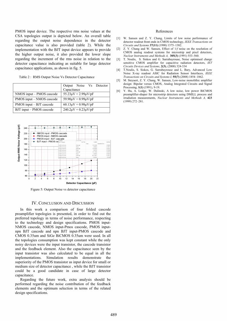
PMOS input device. The respective rms noise values at the CSA topologies output is depicted below. An overall table regarding the output noise dependence in the detector capacitance value is also provided (table 2). While the implementation with the BJT input device appears to provide the higher output noise, it also provided the lower slope regarding the increment of the rms noise in relation to the detector capacitance indicating as suitable for large detector capacitance applications, as shown in fig. 5.
Table 2 : RMS Output Noise Vs Detector Capacitance
Output Noise Vs Detector Capacitance
NMOS input – PMOS cascode 55.23μV + 2.99μV/pF PMOS input – NMOS cascode 59.90μV + 0.99μV/pF PMOS input – BJT cascode 60.13μV + 0.98μV/pF BJT input – PMOS cascode 240.2μV + 0.23μV/pF
Figure 5: Output Noise vs detector capacitance
IV. CONCLUSION AND DISCUSSION In this work a comparison of four folded cascode
preamplifier topologies is presented, in order to find out the preferred topology in terms of noise performance, respecting to the technology and design specifications. PMOS input-NMOS cascode, NMOS input-Pmos cascode, PMOS input-npn BJT cascode and npn BJT input-PMOS cascode and CMOS 0.35um and SiGe BiCMOS 0.35um were used. In all the topologies consumption was kept constant while the only noisy devices were the input transistor, the cascode transistor and the feedback element. Also the capacitance seen by the input transistor was also calculated to be equal in all the implementations. Simulation results demonstrate the superiority of the PMOS transistor as input device for small or medium size of detector capacitance , while the BJT transistor could be a good candidate in case of large detector capacitance.
Regarding the future work, extra analysis should be performed regarding the noise contribution of the feedback elements and the optimum selection in terms of the related design specifications.
References [1] W. Sansen and Z. Y. Chang, Limits of low noise performance of
detector readout front ends in CMOS technology, IEEE Transactions on Circuits and Systems 37(11) (1990) 1375–1382.
[2] Z. Y. Chang and W. Sansen, Effect of 1/f noise on the resolution of CMOS analog readout systems for microstrip and pixel detectors, Nuclear Instruments and Methods A, 305(3) (1991) 553–560.
[3] T. Noulis, S. Siskos and G. Sarrabayrouse, Noise optimised charge sensitive CMOS amplifier for capacitive radiation detectors, IET Circuits Devices and Systems, 2(3), (2008) 324-334
[4] T.Noulis, S. Siskos, G. Sarrabayrouse and L. Bary, Advanced Low Noise X-ray readout ASIC for Radiation Sensor Interfaces, IEEE Transactions on Circuits and Systems I, 55(7) (2008) 1854–1862.
[5] M. Steyaert, Z. Y. Chang, W. Sansen, Low-noise monolithic amplifier design: Bipolar versus CMOS, Analog Integrated Circuits and Signal Processing, 1(1) (1991), 9-19.
[6] Y. Hu, A. Lodge, W. Dulinski, A low noise, low power BiCMOS preamplifier-shaper for microstrip detectors using DMILL process and irradiation measurements, Nuclear Instruments and Methods A, 423 (1999) 272–281.
489