ni labview embedded platform evaluation kit...
TRANSCRIPT

ni.com/embeddedeval Page 1
NI LabVIEW Embedded Platform Evaluation Kit Tutorial
Welcome to the LabVIEW Embedded Platform Evaluation Kit tutorial. This document contains step-by-step instructions for getting started with National Instruments embedded software and hardware, specifically the LabVIEW Real-Time and LabVIEW FPGA development modules and the NI Single-Board RIO hardware platform. The entire NI Embedded platform includes a wide range of hardware and software products for embedded programming beyond those tools covered in this evaluation kit, visit ni.com/embeddedeval for more information.
Note: It may be easier to complete the step-by-step exercises if you print this document before proceeding. Otherwise, the table of contents below contain links to the exercises for more convenient navigation of this document.
Table of Contents
Tutorial Overview ................................................................................................................................... 2
Troubleshooting ..................................................................................................................................... 2
Activating LabVIEW ................................................................................................................................ 2
Navigating the Exercises ......................................................................................................................... 3
Getting Started – LabVIEW Programming Basics ................................................................................... 4
EXERCISE 1 – Open and Run an FPGA Application ................................................................................. 5
EXERCISE 2 – Create an FPGA Application ............................................................................................ 11
EXERCISE 3 – Open and Run an RT and FPGA Application ................................................................... 23
EXERCISE 2 (CONTINUED) – Deploy and Run Exercise 2 ...................................................................... 29
EXERCISE 4 – Add Real-Time Code to an FPGA Application ................................................................. 31
EXERCISE 4 – Part II: Creating a Web Interface .................................................................................... 49
EXERCISE 4 – Part III: Transfer Logged Data to host and view ............................................................. 55
Explore Additional Examples ................................................................................................................ 57
Error Code: -63192 ............................................................................................................................... 58
Changing the IP Address in the LabVIEW Project ................................................................................. 59

ni.com/embeddedeval Page 2
Tutorial Overview
In this tutorial, you will complete four exercises that demonstrate how to use LabVIEW to create embedded real-time and field-programmable gate array (FPGA) applications:
Exercise 1 – Open and run a precompiled FPGA application and review the documentation of the source code to understand how the FPGA application works.
Exercise 2 – Create an FPGA application on your own. While this application is compiling, complete Exercise 3.
Exercise 3 – Open and run a precompiled real-time and FPGA application and review the source code documentation to understand this more complex exercise.
Exercise 4 – Extend the FPGA application you created in Exercise 2 to interface with an application executing on the reconfigurable I/O (RIO) device MPU and create a web interface.
After completing these exercises, explore a variety of real-time and FPGA applications in the “Additional Examples” folder or visit ni.com/embeddedeval. These exercises will demonstrate how to implement common embedded programming tasks and functions using LabVIEW.
Troubleshooting
If you have any questions or run into any configuration issues while exploring this evaluation kit, please review the LabVIEW Embedded Platform Evaluation Kit FAQ online. This document contains information on how to change your IP address or reconnect to your device, and includes answers to basic FPGA compilation questions.
Activating LabVIEW
If you are using an evaluation version of LabVIEW, you will be prompted to activate LabVIEW when you open the environment. To continue in evaluation mode, click the “Launch LabVIEW” button.

ni.com/embeddedeval Page 3
Navigating the Exercises
The LabVIEW Embedded Platform Evaluation Kit installs several helpful exercises on your development machine that you can explore to learn more about LabVIEW Real-Time and FPGA software. By default, these exercises install on your computer’s C: drive at
C:\Documents and Settings\All Users\Documents\National Instruments\Embedded Evaluation\Tutorials
Alternatively, you may locate these files from the Start menu at All Programs > National Instruments > Embedded Evaluation > Tutorial Folder. The original files are also located on the DVD included in the evaluation kit.

ni.com/embeddedeval Page 4
Getting Started – LabVIEW Programming Basics
If you are new to LabVIEW, this section will help you learn more about the LabVIEW development environment and graphical programming language. You can also use the web links in your exercise folder to view Getting Started with LabVIEW videos and online demonstrations. This tutorial assumes you ran the LabVIEW Embedded Platform Evaluation Setup utility upon reboot. If you have not done so, run it now. You can access the utility from your Windows Start menu, select All Programs > National Instruments > Embedded Evaluation > Setup Utility. The hardware device included in your kit is based on the NI Single-Board RIO (reconfigurable I/O) platform and presents a hardware architecture found on other NI RIO devices which consist of two processing devices: a real-time processor that you can program with the LabVIEW Real-Time Module and an FPGA that you can program with the LabVIEW FPGA Module. These devices are connected by a PCI bus and the LabVIEW development environment includes built-in interfaces for communicating between them. The hardware device in your kit will be referred to as your “RIO device” in this tutorial. A LabVIEW application is called a “VI”, or virtual instrument, and is composed of two primary elements: a front panel and a block diagram, which you can program using the LabVIEW Functions Palette.
Front panel – The front panel is what you use to create a LabVIEW user interface (UI). For embedded applications, such as FPGA applications, you either create subfunctions or subVIs where controls and indicators are used to pass data within the target application or you use the front panel to define sockets/registers that are exposed to other elements of your system (such as the real-time processor) with read/write access.
o Note: If you close the front panel, it will also close the block diagram, so be sure to minimize it instead if you wish to use the block diagram.
Block diagram – The block diagram is where you program LabVIEW applications using a combination of graphical and textual notations. To program the block diagram, right-click anywhere on the diagram (blank white window) to bring up the Functions palette.
Functions palette – The Functions palette contains components for creating FPGA, RT, and host interface applications. To do this, place the components on the block diagram and wire them together.
Using the functions palette – In this tutorial, blue, bold text denotes an item to select from the Functions palette. To access the Function palette, right-click anywhere on the LabVIEW block diagram.
You can also “pin” the functions palette so that it is always present on the block diagram. More on Using LabVIEW - You can use access the “.\0 – LabVIEW Programming Basics” folder (if you cannot locate the folder, see Navigating the Exercises from earlier in this document) to learn more about the LabVIEW graphical programming environment including syntax, deployment, debugging, and more. You can also review the short introduction video located in the “.\Additional Resources” folder.

ni.com/embeddedeval Page 5
EXERCISE 1 – Open and Run an FPGA Application
1. Open “.\1 - Open & Run FPGA Example\ Example 1 (Simple FPGA Application).lvproj”. (See Navigating the Exercises earlier in this document if you need assistance locating this folder.)
2. Change the IP address of the RT Single-Board RIO item in the Project Explorer window to match the IP address of your evaluation board.
a. Right-click the RT Single-Board RIO item in the Project Explorer window and select Properties from the shortcut menu to display the General properties page.
b. In the IP Address/DNS Name text box, enter the IP address you wrote down from the National Instruments Embedded Evaluation Setup utility and click OK.
(If you forgot to write down the IP address from the National Instruments Embedded Evaluation
Setup utility and need to determine the IP address of your RIO device, see Changing the IP Address in the LabVIEW Project at the end of this document for further instructions.)
3. Expand the RIO device by clicking the + symbol next to RT Single-Board RIO item in the Project Explorer window. This shows the resources for your embedded evaluation hardware including the code, libraries, and supporting documentation for code that will execute on the device.
4. Expand the FPGA resource on your RIO device by clicking the + symbol next to the FPGA target item under the RIO device in the Project Explorer window. This view shows all the resources available on the FPGA of your RIO device and contains the code, libraries, and supporting documentation for code that will execute on the FPGA.
5. Double-click the Simple Counter Example.vi
to open the FPGA application.

ni.com/embeddedeval Page 6
6. You will see the following front panel when you open the Simple Counter Example.vi:
7. Select Window » Show Block Diagram from the menu bar of the Simple Counter Example.VI front panel (or press <Ctrl-E>) to display the source code or block diagram for the FPGA application.
8. Click the Run button to download and run the application on the FPGA of your RIO device.
9. Interact with your application after it is deployed by turning the encoder knob on your RIO device and observing the incrementing count on the LED bank.

ni.com/embeddedeval Page 7
10. Stop your application by left-clicking the Abort Execution button.
11. Review the following documentation to understand how the LabVIEW FPGA code implements
the FPGA application functionality.

ni.com/embeddedeval Page 8
In Exercise 1, the FPGA application reads a digital input from channel A of the quadrature encoder and counts the number of rising edge events. The application then displays the Boolean representation of the count on the eight LEDs. Because this is an 8-bit counter, the count rolls over after 255 events have been detected.
Context Help – The Context Help window in LabVIEW is a valuable tool for learning the language and understanding the functionality of intellectual property (IP) blocks. Select Help»Show Context Help (or press <Ctrl-H>) to open the Context Help window.
Once opened, the Context Help window displays documentation for the block diagram element on which you place the mouse pointer. The image to the right is an example of the Context Help window for the Event Counter – simple.vi.
Code inside a Single-Cycle Timed Loop executes continuously based on a specified
clock (default 40 MHz)
Counter (8-bit)
digital inputs
digital outputs
Converts count to binary representation

ni.com/embeddedeval Page 9
Open IP Block – You can view the LabVIEW source code of IP blocks that are not primitives.
12. To open the Event Counter IP, double-click the Event
Counter VI icon on the block diagram to open the Event Counter VI. The first window to open is the front panel (shown here). Recall that for FPGA applications developed with the LabVIEW FPGA Module, the block diagram is where you define the logic of the application.
13. Select Window»Show Block Diagram (or press <Ctrl-E>) to
view the block diagram below.
Event Counter – simple.vi IP Details:
Congratulations! You have successfully run a LabVIEW FPGA application on your RIO device.
Close this project and all associated LabVIEW VIs by selecting File»Close All… in the LabVIEW Project Explorer window.
Compare the current digital input to the previous input to determine if a rising edge has occurred
Reset the count to 0 when reset is asserted
Boolean inputs
Counter register (8-bit)
Increment the count if a rising edge has occurred

ni.com/embeddedeval Page 10
In the next exercise, you will build a complete FPGA application, compile it, and deploy it to the FPGA on your RIO device.

ni.com/embeddedeval Page 11
EXERCISE 2 – Create an FPGA Application
In Exercise 1, you opened a precompiled FPGA application and ran it on your RIO device. In this exercise, you will build a complete FPGA application, compile it, and deploy it to the FPGA on your RIO device. You will begin by opening a pre-created blank project from the exercise folder and ensuring you have a connection to your RIO device.
1. Open “.\2 - Create FPGA Personality\Example 2 (LED Control).lvproj.”
(See Navigating the Exercises if you need assistance locating this exercise.)
2. Change the IP address of the RT Single-Board RIO item in the Project Explorer window to match the IP address of your evaluation board.
a. Right-click the RT Single-Board RIO item in the Project Explorer window and select Properties from the shortcut menu to display the General properties page.
b. In the IP Address/DNS Name text box, enter the IP address you wrote down from the National Instruments Embedded Evaluation Setup utility and click OK.
3. Expand the RIO device by clicking the + symbol next to the RT Single Board RIO item in the Project Explorer window. This view shows all the resources available on your embedded

ni.com/embeddedeval Page 12
evaluation hardware and contains the code, libraries, and supporting documentation for code that will execute on the device.
4. Expand the FPGA resource on your RIO device by clicking the + symbol next to the FPGA target
item under the RIO device in the Project Explorer window. This view shows all the resources available on the FPGA of the RIO device and contains the code, libraries, and supporting documentation for code that will execute on the FPGA.
5. Right-click the FPGA Target in the Project Explorer window and select New»VI.
You will then see a blank VI (front panel and block diagram).
LabVIEW Project
LabVIEW Block Diagram
LabVIEW Front Panel

ni.com/embeddedeval Page 13
Application Overview The application you will build reads the analog value of a potentiometer with a range of 0 to 4 VDC and displays its relative value on a bank of eight LEDs. In this design, the FPGA application will scale the potentiometer input to a range of 0 to 8 with a resolution of 1. The FPGA application will then map the scaled range to the bank of 8 LEDs. The diagram below shows the FPGA code you will create in this exercise. The remaining steps in this exercise will guide you through the creation of this FPGA application in LabVIEW.
Read Analog Value from Potentiometer – RIO devices offer a variety of interfaces including analog I/O (AIO), digital I/O (DIO), digital communications protocols, specialty I/O, and memory. You can use the FPGA I/O Node to implement read/write operations to these interfaces. 6. Start from the block diagram (Window>>Show Block Diagram or Ctrl + E) and right-click to
access the Functions palette. You can also “pin” the functions palette so that it is always present on the block diagram. To select functions, left-click the specified object and left-click a second time to place or drop the object onto the block diagram.

ni.com/embeddedeval Page 14
7. Select Programming»FPGA I/O»I/O Node from the Functions palette and place the FPGA I/O Node on the left side of the block diagram.
8. Configure the FPGA I/O Node to read from the potentiometer analog input channel. a. Left-click I/O Item on the FPGA I/O Node and select Eval Acc IO»AI»POT.
Scale Input for LED Display – The potentiometer returns a value between 0 and 4 VDC in increments of 4.7684E-7 VDC. In this section, you will scale that input to an integer value between 0 and 7 to match the indexed range of the LED bank.
9. Select Programming»Numeric»Multiply from the Functions palette and place the Multiply function to the right of the FPGA I/O Node you configured in the previous section.
10. Connect the output of the potentiometer read to the x input of the multiply function. a. Place your mouse pointer on the right edge of the black arrow on the right side of the
FPGA I/O Node (POT output terminal) and left-click.
b. Place your mouse pointer over the top-left corner of the Multiply function (x input
terminal) and left-click to complete the wire.
11. Create a constant for the y input of the Multiply function. a. Right-click the y input terminal of the Multiply function and select Create»Constant.

ni.com/embeddedeval Page 15
b. Double-click the constant box and type 2 to replace the default constant value of 0. (Note: By default, LabVIEW displays the trailing zeros on fixed-point constants. To adjust this setting, right-click the constant and select Properties from the shortcut menu to display the Numeric Constant Properties dialog box, then place a checkmark in the Hide trailing zeros checkbox on the Display Format tab.)
12. Select Programming»Numeric»Round To Nearest from the Functions palette and place the Round To Nearest function to the right of the Multiply function on the block diagram.
13. Connect the output of the Multiply function to the input of the Round To Nearest function. a. Place your mouse pointer over the right corner of the Multiply function (x*y output
terminal) and left-click. b. Place your mouse pointer over the left side of the Round To Nearest function (number
input terminal) and left-click to wire these icons together.
Update LED Bank Register – To write to the bank of eight LEDs on the hardware, create a register using an array of Boolean values. Depending on the scaled value of the potentiometer, the FPGA application will assert one of the eight array elements, illuminating the corresponding LED. In this section, you will create the code to update the appropriate element based on the scaled potentiometer value.
14. Select Programming»Array»Array Constant from the Functions palette and place the
Array Constant to the right and above the Round To Nearest function.
15. Select Programming»Boolean»False Constant from the Functions palette and place the False Constant inside the Array Constant.
16. Right-click the “0” in the Array Constant and select Set Dimension Size to specify the size of the array.

ni.com/embeddedeval Page 16
a. Change the size from variable to fixed. b. Set the number of elements to eight.
c. Resize the Array Constant to show all eight elements by left-clicking
and holding on the bottom edge of the right-half of the Array Constant and dragging it down to expose eight false constants.
17. Select Programming»Array»Replace Array Subset from the Functions palette and place the Replace Array Subset function to the right of the Round To Nearest function.
18. Connect the Array Constant output to the array input terminal of the Replace Array Subset
function.
19. Connect the nearest integer value output of the Round To Nearest function to the index input
of the Replace Array Subset function.
Note: In this application, the Round To Nearest function can output 9 possible values (0 – 8). However, the RIO device contains only 8 LEDs (0 – 7). Therefore, when the potentiometer is turned all the way up, the Replace Array Subset function attempts to write to an array index that does not exist. By default, the LabVIEW FPGA Module handles this situation by performing no operation on the array.
20. Create a True constant for the new element/subarray input terminal of the Replace Array
Subset function.

ni.com/embeddedeval Page 17
Write to LED Bank – Now that you have created an LED bank register, you need to map the register to the LED bank so changes to the register are written to the LED bank.
21. Select Programming»Array»Index Array from the Functions palette and place the Index Array function to the right of the Replace Array Subset function.
22. Connect the output array terminal of the Replace Array Subset function to the array
terminal of the Index Array function .
23. Expand the Index Array block to show eight output terminals. a. Place your mouse over the bottom edge of the Index Array block and click-and-hold the
left mouse button to drag the icon down until eight output terminals are exposed on the right side of the Index Array function.
24. Select Programming»FPGA I/O»I/O Node from the Functions palette and place an FPGA I/O Node to the right of the Index Array function.
25. Configure the FPGA I/O Node to write to the LED bank. a. Left-click I/O Item on the FPGA I/O Node and select Eval Acc IO»LED»LED 0. b. Right-click LED 0 on the FPGA I/O Node and select Change to Write.
Replace Array Subset

ni.com/embeddedeval Page 18
c. Place your mouse pointer over the bottom edge of the FPGA I/O Node and click-and-hold the left mouse button to expand the node until LED 0 through LED 7 are exposed.
26. Connect the Index Array output terminals to the corresponding FPGA I/O Node input terminals
as shown below. a. Note: Do not be concerned about overlapping wires. After you connect all the terminals,
use the Clean Up Diagram tool to automatically clean up your block diagram – see below or use the keyboard shortcut <Ctrl+U>.
Create Socket/Register for real-time Code – Although it is not necessary for this exercise, in Exercise 4 you will extend this exercise to interface with code running on the RIO device real-time processor. To avoid the need to recompile the FPGA application, add a socket now so that the RT application you create in Exercise 4 can read the current value of the potentiometer. 27. Place your mouse pointer over the wire leaving the FPGA I/O Node POT output that is reading
from the potentiometer, right-click, and select Create Indicator. After using the Diagram Clean Up tool (Ctrl+U) again, you should have a block diagram that looks similar to the one below:

ni.com/embeddedeval Page 19
Specify Execution Timing – If the FPGA application you just created was compiled and run at this point, it would execute only once. You can specify continuous execution of your application by using a looping structure. There are several looping structures available in the LabVIEW FPGA Module. For this exercise, you will use a While Loop. This loop structure specifies that your circuit executes continuously. You can slow the execution speed down using a function from the Timing palette or speed it up by changing the default clock rate for your FPGA target. 28. Place a While Loop around the complete circuit.
a. Select Programming»Structures»While Loop from the Functions palette. b. Move your mouse pointer to the top-left side of your code and left-click. c. Move your mouse pointer to the bottom-right side of your code so the entire block of
code is contained in the dashed box and left-click. Note: Another method to create the While Loop is to left-click-and-hold in step b (instead of releasing the mouse button) and drag to the other corner of the While Loop before releasing the mouse button.

ni.com/embeddedeval Page 20
d. Place your mouse pointer over the red stop icon in the bottom-right of the While Loop, right-click, and select Create >> Constant. Note: The red stop icon is the stop condition for the While Loop; wiring a False constant to the stop condition specifies that the code will run indefinitely.

ni.com/embeddedeval Page 21
Compile and Run FPGA Application – Your FPGA application is complete. Save your project and begin compiling your FPGA application so it can execute on the FPGA.
29. Save your FPGA application if you have not already done so. a. Select File»Save from the menu bar and save the FPGA application as “.\2 - Create FPGA
Personality\FPGA Personality\Display POT Value.vi.” 30. Compile and run your application.
a. Click the Run button on the block diagram or front panel of the FPGA VI to start the compilation process. During compilation, LabVIEW displays the Generating Intermediate Files dialog box.
At this point, LabVIEW is generating VHDL code based on the LabVIEW FPGA VI you created. Note: The process of synthesizing VHDL can take anywhere from a few minutes to several hours depending on the complexity of the design and the performance of the development machine. This particular example takes approximately 10 minutes on a modern desktop PC. The actual compile time depends on the speed of your PC and what other applications are running during the compile. To improve development efficiency, LabVIEW provides system simulation capability allowing you to simulate the FPGA application, RT application, host interface, I/O, and even a model of the environment your embedded device will interact with on deployment. Visit ni.com/embeddedeval for more information. After the VHDL code generation is complete, you will see the Compile Status dialog box appear briefly followed by the LabVIEW FPGA Compile Server dialog box. While the compile is taking place, the Compile Status dialog box returns to the foreground when you click a LabVIEW window other than the LabVIEW FPGA Compile Server window.

ni.com/embeddedeval Page 22
While this compile is taking place (estimated 10 minutes), you can do one of two things:
1. Wait for the compile to complete and skip to the Deploy and Run Exercise 2 section (be sure to
return to Exercise 3 when you are finished with this section).
2. RECOMMENDED - Start working on Exercise 3 and complete the Deploy and Run Exercise 2 section after you finish Exercise 3 (at that point the compile should be complete). If you choose this option, you will need to first disconnect from the LabVIEW FPGA Compile Server so that you can continue to work in LabVIEW:
a. Select the Compile Status window
from the Windows task bar.
b. In the Compile Status dialog box, click the Disconnect button
c. Minimize, but do not close, all of
the LabVIEW windows that are currently open:
Example 2 (LED Control).lvproj
Display POT Value.vi Front Panel
Display POT Value.vi Block Diagram
LabVIEW FPGA Compile Server You will reconnect to the LabVIEW FPGA Compile Server in the Deploy and Run Exercise 2 section after you finish Exercise 3.
Compile Status
LabVIEW FPGA Compile Server

ni.com/embeddedeval Page 23
EXERCISE 3 – Open and Run an RT and FPGA Application
In the previous two exercises, you worked only with the FPGA resource on your RIO device. In this exercise, you will open and run an application that uses both the MPU and the FPGA resources on your RIO device.
The RIO Architecture: The RIO architecture consists of an embedded microprocessor (MPU) connected to an FPGA which is connected to a variety of I/O interfaces. Both the MPU and the FPGA are programmed using LabVIEW and can incorporate traditional text-based code (C, VHDL, Verilog, etc) to provide a powerful and highly efficient Graphical System Design platform.
NI provides a variety of off-the-shelf hardware platforms based on this architecture to address different application requirements including: cost, performance, flexibility, footprint, and ruggedness to provide you with a scalable development platform that will allow you to quick design, prototype, and deploy their embedded system. Visit ni.com/embeddedeval for more information.
1. Open “.\3 - Open and Run MPU-FPGA Application\Example 3 (MPU-FPGA application).lvproj.”
(See Navigating the Exercises if you need assistance locating this exercise.) 2. Change the IP address in the project to match the IP address of your RIO device by right-clicking
the RT Single-Board item and selecting properties.
(If you do not have your IP address, see the section on Changing the IP Address in the LabVIEW Project at the end of this document for detailed instructions.)

ni.com/embeddedeval Page 24
3. Expand the RIO device by clicking the + symbol next to your RIO device to view the resources
available on your RIO device for code that will execute on the MPU.
4. Expand the FPGA resource on your RIO device by clicking the + symbol next to the FPGA target for your RIO device to view all the resources available on the FPGA of your RIO device.
5. Double-click FPGA Personality (example3).vi to open the FPGA application.
6. Select Window»Show Block Diagram from the menu bar (or press <Ctrl-E>) to display and explore the source code for the FPGA application.
7. Double-click RT MPU.vi to open the real-time application.

ni.com/embeddedeval Page 25
8. Select Window»Show Block Diagram from the menu bar (or press <Ctrl-E>) to display source code for the real-time MPU application.
9. Click the white run arrow to download the MPU code to the microprocessor on your RIO device.
The MPU code will load and run the FPGA application, FPGA Personality (example 3).vi, when it initializes. (If your receive error -63192, see the Error Code: -63192 section at the end of this document.)
10. Interact with the application after it deploys. a. Turn the potentiometer knob and observe the signal on the user interface. b. Change the trigger parameters in the user interface. c. Place your finger over the temperature sensor and observe the signal on the user
interface. d. Turn the encoder knob and observe the incrementing count on the LED bank and the
user interface.
11. Review the documentation below to understand how the LabVIEW code implements the
application functionality.

ni.com/embeddedeval Page 26
FPGA Application Overview – This FPGA application demonstrates a variety of tasks including: AIO/DIO, event counting, sine wave generation, data type casting, triggering, register communication with MPU, and DMA streaming to MPU. To view the implementation details of any block, use the Context Help Window by selecting Help » Show Context Help from the menu bar.
Digital Counter Loop – this loop performs the same functionality as the example in Exercise 1, however it only displays the four least significant bits of the 8-bit counter on the LED bank (the other four LEDs are used by the Analog Input w/ Counter & Trigger loop).
Signal Generation Loop – This loop generates a sine wave on channel AO0.
Analog Input w/ Counter & Trigger Loop – this loop performs a continuous acquisition of 3 analog signals (potentiometer, sine wave generated by Signal Generation loop, and temperature sensor). The potentiometer value is used as an input to the Hysteresis Trigger function whose settings can be adjusted via the Trigger Config Register. The number of triggers are counted and displayed on the other four LEDs. The trigger signal as well as the three analog signals are converted to a U32 data type and streamed to the MPU application via a DMA FIFO. DMA FIFOs provide the greatest throughput for moving data between the FPGA and real-time applications and are typically used for high-speed and/or continuous data transfer tasks.

ni.com/embeddedeval Page 27
Real-Time Application Overview – This application demonstrates how a real-time application is implemented on the real-time MPU of your RIO device. When running this example, you will be using the LabVIEW Default Communication which automatically provides a user interface to the embedded application running on the MPU via the Front Panel. This interface is typically used during application development as a debugging interface. For deployed applications, a web interface is typically used to provide interaction with the embedded application. In Exercise 4, you will use the LabVIEW Web Publishing Tool to automatically create a web interface to the embedded application.
Note: the green and brown wires between the purple FPGA Interface blocks are used to pass the FPGA resource reference and error information respectively. Notice that the error wire is used as a stop condition for the While Loop. The terminals (Trigger Configuration, Count Reg, Trigger …) which are used as registers on the FPGA application are used to communicate with the Front Panel objects of your MPU application. The Front Panel of the MPU application provides a user interface to your embedded application.
Connect to FPGA and download
personality
Loop timing (execute once
per millisecond)
Read from DMA FIFO
R/W registers on FPGA
Convert data from DMA and write to
front panel indicators
Stop execution on user input or application error
Close connection
to FPGA

ni.com/embeddedeval Page 28
12. Stop your application by clicking the stop button on your host interface front panel.
Congratulations! You have successfully run a LabVIEW FPGA application on your RIO device.
Close this project by selecting File»Exit from the RT MPU.vi front panel. If you have not completed the Deploy and Run Exercise 2 section, proceed to that section, otherwise skip to Exercise 4 where you will extend the LabVIEW FPGA application you created in Exercise 2 by adding a real-time application that includes a web interface.

ni.com/embeddedeval Page 29
EXERCISE 2 (CONTINUED) – Deploy and Run Exercise 2
1. If you disconnected from the LabVIEW FPGA Compile Server in Exercise 2, reconnect and run your FPGA application (see bullets below). Otherwise, if you finished Exercise 2 and waited for the compile, skip to Step 2.
a. Restore the project you were working in during Exercise 2 (should be minimized in your Windows task bar).
b. Right-click your FPGA application (Display POT Value.vi) from your Exercise 2 project and select “Reconnect to Compilation”.
2. Close the Successful Compile Report window by selecting OK.
3. Close the LabVIEW FPGA Compile Server window.
4. Select File»Save All in the LabVIEW Project Explorer menu bar.

ni.com/embeddedeval Page 30
5. Open your FPGA application (Display POT Value.vi) and click the white run arrow to download
and deploy your application to the RIO device. (If your receive error -63192, see the Error Code: -63192 section at the end of this document.)
6. Turn the potentiometer knob of your evaluation board once your FPGA application is running and observe the behavior of the LED bank.
7. Stop your application by left-clicking the Abort Execution button.
Congratulations! You have successfully created a LabVIEW FPGA application on your RIO device.
Close this project selecting File»Exit from the LabVIEW front panel. In the next exercise (Exercise 4), you will extend the LabVIEW FPGA application you created in Exercise 2 by adding a real-time application that includes a web interface.

ni.com/embeddedeval Page 31
EXERCISE 4 – Add Real-Time Code to an FPGA Application
In Exercise 2, you created an FPGA application that reads the value of the potentiometer channel and displays the relative value on the LED bank. In this exercise, you will add a real-time application that:
Logs the data to non-volatile storage on your RIO device when the value exceeds a user-defined threshold
Displays a histogram and time-history plot of the potentiometer data on a web interface
Open FPGA Project and Add Real-Time Application – Begin with the compiled FPGA application you completed in Exercise 2..
1. Open “./2 – Create FPGA Personality/Exercise 2 (LED Control).lvproj”. Alternatively, use the solution for Exercise 2 location at “./2 – Create FPGA Personality/_Solution/Exercise 2 (LED Control).lvproj”.
2. If necessary, change the IP address in the project to match the IP address of your RIO device.

ni.com/embeddedeval Page 32
(see the section on Changing the IP Address in the LabVIEW Project at the end of this document for detailed instructions if you cannot locate your IP address.)
3. Expand the RIO device by clicking the “+” symbol next to your RIO device IP address. Recall that
this level shows all the resources available on your embedded evaluation hardware.
4. Right-click on the RT Single-Board RIO Device and select Add»File…
5. Navigate to and add a partially complete VI located at “.\4 - Create MPU-FPGA Application\MPU Code/RT MPU.vi”.

ni.com/embeddedeval Page 33
6. Expand the FPGA resource on your RIO device by clicking the “+” symbol net to the FPGA target for your RIO device. Recall that this level shows all the resources available specifically on the FPGA of your RIO.
7. Confirm that the Project Explorer now contains both the FPGA application you created in Exercise 2 (Display POT Value.vi) and the real-time RT MPU.vi.
Complete User Interface – LabVIEW makes it very easy to rapidly create rich user interfaces for debugging and deployment interaction. In this exercise, you will update a partially complete Front Panel that will be used to interact with the real-time application you will create in subsequent steps of this exercise.

ni.com/embeddedeval Page 34
8. Double-click on RTMPU.vi to open the partially complete real-time application. You will notice
that part of the UI has already been built.
Add a stop button and trigger threshold input control before begin writing code. You will add additional items to the interface as you write your REAL-TIME application in the next several sections.
a. Right-click anywhere on the Front Panel (gray window) to activate the Controls Palette. Select Modern»Boolean»Stop Button and place the control under the right corner of the POT Data chart. Once placed, you can resize and customize as you wish.
>> >> (You can also pin the Controls Palette by using the pin icon in the top left corner of the Controls Palette - avoiding the need to right-click each time you’d like to access the palette.) b. Again, right-click anywhere on the Front Panel (gray window) to activate the Controls
Palette. Select Modern»Numeric»NumericControland place the control under the left corner of the POT Data chart.
c. You can right-click on any of the Front Panel objects to adjust the appearance, display, and other settings for the object. Select the Properties item in the drop down menu display a comprehensive dialog that will allow you to adjust numerous settings for the object.
d. Double-click on the ‘Numeric’ text label of the Numeric Control object you placed in step b above. This will highlight the text and allow you to change the label for the object to “Trigger Level”.

ni.com/embeddedeval Page 35
9 . Double-click on one of the Front Panel objects to open the Block Diagram, select Window >> Show Block Diagram or use the Ctrl + E shortcut key. Notice there are terminals on the block diagram that correspond to the objects on the Front Panel which are used to pass data to and from the user interface (Front Panel). You will also notice that the data logging portion of the application has already been created. In the following sections, you will use LabVIEW to create the application that will execute on the real-time processor of your RIO device. Before you proceed, locate the ‘stop’ and ‘Trigger Level’ terminals corresponding to the Front Panel objects you just created. Move them so that they are positioned above the ‘LOGGING LOOP (gated trigger)’ code that has already been created for you.

ni.com/embeddedeval Page 36
Create Link to FPGA Resource – the following steps will specify which FPGA application is to be loaded to the FPGA on your RIO device when the real-time application is run. 10. Select FPGA Interface»Open FPGA VI Reference from the Functions palette and place it on the left side of your diagram above the Logging Loop. 11. Right-click on the Open FPGA VI Reference object and select ‘Configure Open FPGA VI Reference…’
12. Select the ‘VI’ option, choose ‘Display POT Value.vi’ and press “OK” in the dialog to specify the FPGA application you created in Exercise 2 will be loaded and run on the FPGA when this function is called.

ni.com/embeddedeval Page 37
13. Select “OK” in the Configure Open FPGA VI Reference dialog to close. Read Potentiometer Value and Display – The following steps will read the value of the potentiometer that is acquired by your FPGA application (‘Display POT Value.vi’).
14. Select FPGA Interface»Read/Write Control from the Functions palette and place it on the right of the ‘Open FPGA VI Reference’ function you just placed.
15. Connect the ‘FPGA Reference’ and ‘error’ terminals of the two FPGA objects you just placed as shown below.
Remember to use Context Help (Ctrl + H) to find useful information about the functions you are programming with including details on the FPGA reference and Error wires.
FPGA Reference wire –passes a reference to the FPGA application specified in the ‘Open FPGA VI Reference’ function to other FPGA interface functions in your application. Error wire –is a data structure used to communicate errors in LabVIEW applications. This structure includes a Boolean value signaling whether the error status, a integer value corresponding to the error if one occurred (which can be used by a error handling routine), and a string that provides a description of the error which can be displayed in the user interface (if there is one) or logged (typical error handling technique for embedded applications).

ni.com/embeddedeval Page 38
16. Left-click on ‘Unselected’ in the Read/Write Control and select ‘POT’ to specify that this function is to read from the POT register of your FPGA application.
Evaluate Trigger and Update Histogram – The following steps will generate the code to evaluate the trigger condition, update a histogram of the potentiometer data, and update the corresponding indicators on your display.
17. Select Programming»Numeric»Conversion »To Double Precision Float from the Functions Palette and place it on the right of the ‘Read/Write Control’ function you just placed. This function will convert the fixed-point data received from your FPGA applications to a double precision floating point data type.
18. Wire the ‘POT’ output of the ‘Read/Write Control’ function to the ‘number’ (left) input terminal of the ‘To Double Precision Float’ function you just placed.

ni.com/embeddedeval Page 39
19. Right-click on the ‘double precision float’ (right) output terminal and select Create»Indicator from the drop-down menu to automatically create an indicator on your Front Panel and rename it to ‘POT Value’ by double-clicking on the ‘double precision float’ text.
20. Connect the output of the ‘To Double Precision Float’ function to the ‘POT Data’ terminal a. Left-click on the ‘double precision float’ (right) output terminal of the ‘To Double
Precision Float’ function. b. Left-click on the left side of the ‘POT Data’ terminal to complete the wire.
21. Select Signal Processing»PointBby Point» Probability & Statistics PtByPt»Histogram PtByPt.vi from the Functions palette and place it below and to the right of the ‘To Double Precision Float’ function.
22. Connect the output of the ‘To Double Precision Float’ function to the ‘x’ input terminal of ‘Histogram PtByPt.vi’

ni.com/embeddedeval Page 40
a. Left-click on the ‘double precision float’ (right) output terminal of the ‘To Double Precision Float’ function and wire it to the ‘x’ input terminal (top left) of the ‘Histogram PtByPt.vi’ terminal.
23. Right-click on the ‘Histogram PtByPt.vi’ ‘Histogram Graph’ (top right) output terminal and select Create»Indicator from the drop-down menu to automatically create an indicator on your Front Panel. double-click on the label and rename it ‘Histogram Data’.
24. Select Programming»Syncronization»First Call? from the Functions Palette and place it below the ‘Histogram PtByPt.vi’ function.
25. Wire the ‘First Call?’ object to the ‘initialize’ (bottom) input terminal of ‘Histogram PtByPt.vi’. This will tell the histogram function to initialize on the first iteration of the application.

ni.com/embeddedeval Page 41
26. Select Programming»Comparison»Greater? from the Functions Palette and place it to the left of the ‘Trigger’ indicator terminal.
27. Connect the output of the ‘To Double Precision Float’ function to the ‘x’ input terminal of ‘Greater?’ function.
28. Connect the ‘Trigger Level’ control terminal to the ‘y’ input terminal of ‘Greater?’ function.
29. Connect the ‘x>y?’ output terminal of the ‘Greater?’ function to the ‘Trigger’ indicator terminal.

ni.com/embeddedeval Page 42
Add a Timed Loop Structure – To execute the task you just created continuously, you will place a Timed-Loop around the code. Remember to use Context Help (Ctrl+H) to get more information about the LabVIEW functions you are using.
30. Place a Timed Loop around the code you just created.
a. Select Programming»Structures»Timed Structure»Timed Loop from the Functions palette.
b. Move your mouse pointer to the top-left side of your code (excluding the ‘Open FPGA VI Reference’ function) and left-click.
c. Move your mouse pointer to the bottom-right side of your code so the entire block of code is contained in the dashed box and left-click. Note– Another method to create the Timed Loop is to left-click-and-hold in step b (instead of releasing the mouse button) and drag to the other corner of the Timed Loop before releasing the mouse button.
31. Connect the ‘Stop’ control terminal to the ‘stop condition’ of the Timed Loop.
Complete the Logging Loop – The Logging Loop that was created for you uses ‘Local Variables’ to pass data between the two tasks that execute in parallel. In this section, you will update the local variable that is used to pass the potentiometer data to be logged. Remember that you can use the Context Help (Ctrl+H) Window to learn more about the functions used in this task.
32. In the LOGGING LOOP (the timed loop below the one you just created), left-click on the ‘?’ enclosed in a black box and select ‘POT Value’ form the drop-down menu. This will link the input to the Write Data VI to the potentiometer value that is read from the FPGA application.

ni.com/embeddedeval Page 43
33. Timed Loops are specialized While Loops that have many properties which can be easily configured to implement timing, priority, and even processor affinity (for multicore processors). In LabVIEW, parallel loops automatically distribute parallel code across multithreading execution systems and/or multicore processors. Double-left-click the blue box on the top-left of the ‘Logging Loop’ to examine the available settings. Specifically note the ‘Loop name’ as this will be used in the next section.
34. Select “OK” to close this dialog.
Close FPGA resource link and stop logging loop – In this section, you will add additional code to the top loop that will close the connection to the FPGA on your RIO device and stop the LOGGING LOOP when the application is stopped by the ‘stop’ button control on the user interface.
35. Select FPGA Interface»Close FPGA VI Reference from the Functions palette and place it to the right of the top Timed Loop that you created earlier in this exercise.

ni.com/embeddedeval Page 44
36. Connect the FPGA Reference and Error terminals of the ‘Read/Write Control’ and ‘Close FPGA VI Reference’ functions as shown below.
37. Select Programming»Structures»Timed»Structures»Stop Timed Structure.vi from the Functions palette and place it to the right of the ‘Close FPGA VI Reference’ function.
38. Right-click on the ‘name’ (top left) input terminal of the ‘Stop Timed Structure.vi’ function
and select Create»Constant from the drop down menu.
39. Type “LOG_LOOP” in the string constant you just created. Note – you may need to double-click inside the string constant (pink box) in order to enter the value.
40. Connect the ‘error out’ terminal of the ‘Close FPGA VI Reference’ function to the ‘error in (no
error)’ terminal of the ‘Stop Timed Strucutre.vi’ function.
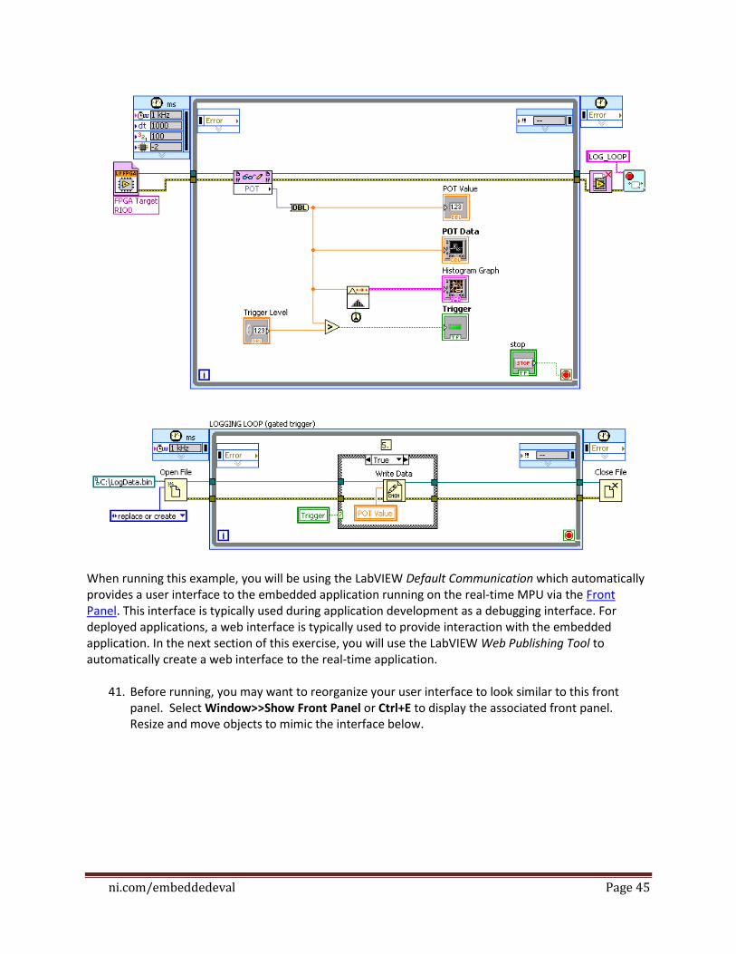
Run and Save – Your real-time application is complete and should look similar to the diagram below.
ni.com/embeddedeval Page 45
When running this example, you will be using the LabVIEW Default Communication which automatically provides a user interface to the embedded application running on the real-time MPU via the Front Panel. This interface is typically used during application development as a debugging interface. For deployed applications, a web interface is typically used to provide interaction with the embedded application. In the next section of this exercise, you will use the LabVIEW Web Publishing Tool to automatically create a web interface to the real-time application.
41. Before running, you may want to reorganize your user interface to look similar to this front panel. Select Window>>Show Front Panel or Ctrl+E to display the associated front panel. Resize and move objects to mimic the interface below.

ni.com/embeddedeval Page 46
42. Click on the Run arrow to download and deploy your application to the RIO device. (If your receive error -63192, see the Error Code: -63192 section at the end of this document.)
ni.com/embeddedeval Page 47
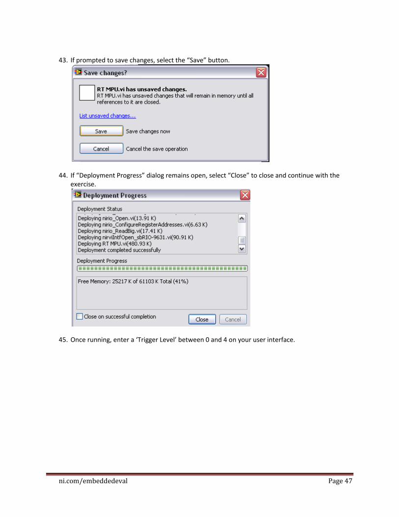
43. If prompted to save changes, select the “Save” button.
44. If “Deployment Progress” dialog remains open, select “Close” to close and continue with the exercise.
45. Once running, enter a ‘Trigger Level’ between 0 and 4 on your user interface.

ni.com/embeddedeval Page 48
46. Turn the potentiometer knob of your evaluation board once your FPGA application downloads to the RIO device and observe the behavior of the LED bank and the displays on your user interface.
47. Stop the application by clicking on the stop button on your user interface.

ni.com/embeddedeval Page 49
EXERCISE 4 – Part II: Creating a Web Interface
Create Web Interface – For deployed embedded applications, you can create a web interface from your Front Panel that will be hosted locally on your RIO device. In this section, you will use the LabVIEW Web Publishing Tool to automatically create a web interface to your application.
1. With the current project still open, select Tools»Web Publishing Tool… from the Project Explorer menu bar to open the LabVIEW Web Publishing Tool.
2. Select your real-time application (‘RT MPU.vi’) in the ‘VI name’ section, select the ‘Embedded’ radio button, check ‘Request control when connection is establish’, and click on ‘Start Web Server’, before clicking ‘Next’.

ni.com/embeddedeval Page 50
3. Enter desired text to be displayed on the web interface in the ‘Document title’, ‘Header’, and ‘Footer’ text boxes before clicking ‘Next’. For example, ‘Document title’ could be “LabVIEW RIO Application”.
4. Click ‘Next’
5. Enter “index” in the ‘Filename’ box and click ‘Save to Disk’.

ni.com/embeddedeval Page 51
6. Click ‘OK’ in the successful save confirmation dialog.
7. Use a FTP utility to transfer the data log file to your development computer. There are many techniques to accomplish this. One is to enter: ftp://<RIO Device IP Address>/ni-rt/system/www/ into your web browser (where <RIO Device IP Address> is the same IP address you have entered in the Project Explorer to identify your RIO Device.

ni.com/embeddedeval Page 52
8. If you see the window above, you will need to select View»Open FTP Site in Windows Explorer in order to manipulate the directory.
9. Delete the current “index.htm” file (if one exists) from the “./ni-rt/system/www” directory.
10. Change the name of the file you just created with the Web Publishing Tool from “index.html” to
“index.htm”. Make sure the file name is “index.htm”.
11. After renaming the file, copy it to the directory webserver directory on your RIO device:
“<RIO device IP Address>/ni-rt/system/www”
12. Return to the Project Explorer window.
13. Right-click on your RIO device in the Project Explorer and select Properties to configure the LabVIEW web server settings for your RIO device.
a. In the ‘Web Server Configuration’ category, check ‘Enable Web Server’ and press ‘OK’.

ni.com/embeddedeval Page 53
14. Return to the front panel of your real-time application (RT MPU.vi) and run the application again by clicking on the Run button.
15. Open a Windows Internet Explorer window and enter the IP address of your RIO device to display the web interface you just created. If you used a file name other than “index.htm” you will also need to add the complete name (name and extension) to the URL after the IP address (example http://<RIO Device IP Address>/WebInterface.html).
NOTE - You must have the LabVIEW Run-time engine installed to use the web interface. This is automatically installed with LabVIEW, however if you use a computer to view the web interface without LabVIEW installed, you will need to download the run-time engine from ni.com.

ni.com/embeddedeval Page 54
Congratulations! You have successfully created a LabVIEW real-time, FPGA and web host interface application.
Close this project selecting File»Close All in the Project Explorer window.
ni.com/embeddedeval Page 55
EXERCISE 4 – Part III: Transfer Logged Data to host and view
The application you created saved a binary data log file to the root directory (C:) of your RIO device. A viewer for these files is included in the exercise directory. In this section, you will transfer the data files to your development computer and view the data that was logged when you ran the application. Note – if the potentiometer value never exceeded the trigger value you specified, there will be no data log file and you will need to run the application again ensuring your potentiometer value exceeds the trigger threshold before completing this section.
1. Use an FTP utility to transfer the data log file to your development computer. There are many techniques to accomplish this. One is to enter ftp://<RIO Device IP Address>/c: into a web browser. The file will be located at “C:\LogData.bin” on your RIO device. Copy this file to your local machine.
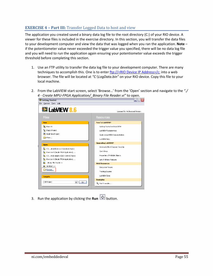
2. From the LabVIEW start screen, select ‘Browse…’ from the ‘Open’ section and navigate to the “./ 4 - Create MPU-FPGA Application/_Binary File Reader.vi” to open.
3. Run the application by clicking the Run button.
ni.com/embeddedeval Page 56
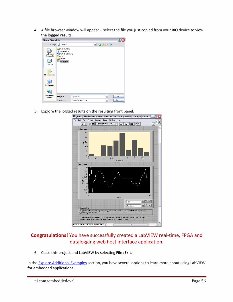
4. A file browser window will appear – select the file you just copied from your RIO device to view the logged results.
5. Explore the logged results on the resulting front panel.
Congratulations! You have successfully created a LabVIEW real-time, FPGA and datalogging web host interface application.
6. Close this project and LabVIEW by selecting File»Exit.
In the Explore Additional Examples section, you have several options to learn more about using LabVIEW for embedded applications.
ni.com/embeddedeval Page 57
Explore Additional Examples
Now that you are familiar with how to create and run FPGA and real-time applications using LabVIEW, you have several options to learn more about using LabVIEW for embedded applications.
1. Explore a variety documented examples that demonstrate how to implement common tasks and functions used in embedded applications using LabVIEW. These examles are ready-to-run on your RIO device include:
Watch dogs
Additional counter implementations
Pulse Width Modulation
FPGA-based Fast Fourier Transform (FFT)
FPGA-based filtering
Quadrature encoder decoding
And many more real-time and FPGA implementations Use the link in the “./5 – Documented Examples” folder on your machine or navigate to ni.com/embeddedeval using your web browser to view a complete list of examples ready-to-run on your RIO device.
2. Your local field engineer is also available to further discuss how LabVIEW software or RIO
hardware can solve your application needs. Simply request a free on-site visit or speak with an expert here.

ni.com/embeddedeval Page 58
Error Code: -63192
If you receive the error dialog below when attempting to run your application, your FPGA Target Resource name needs to be changed.
1. Right-click on your FPGA Target in the Project Explorer window, select Properties and change the FPGA Target Resource to “RIO0”. Close the dialog by selecting “OK’ and run your application again.

ni.com/embeddedeval Page 59
Changing the IP Address in the LabVIEW Project
Your RIO device is identified by its IP address. For each exercise, confirm that the IP address in the project matches the IP address of your RIO device. The National Instruments Embedded Evaluation Setup
utility should have prompted you to write down the RIO device IP address, but you also can locate the
device through the following steps. If you already know your IP address, skip to Step 3.
1. Determine the IP address of your RIO device by opening the Measurement & Automation Explorer with the icon on your desktop or by selecting Start»Programs»National Instruments»Measurement & Automation.
a. Click the + symbol next to Remote Systems.
2. Click the device that appears to locate the IP address.
3. Return to your project, right-click your RIO device, and select properties to update the IP address.