new semiconductor devices - home icmprzyrbwn.icm.edu.pl/app/pdf/114/a114z502.pdf · new...
TRANSCRIPT
Vol. 114 (2008) ACTA PHYSICA POLONICA A No. 5
Proc. XXXVII International School of Semiconducting Compounds, Jaszowiec 2008
New Semiconductor Devices
F. Balestra∗
Sinano Institute, IMEP (CNRS-INPG-UJF), Grenoble INP-Minatec3 Parvis Louis Neel, BP 257, 38016 Grenoble cedex 1, France
A review of recently emerging semiconductor devices for nanoelectronic
applications is given. For the end of the international technology roadmap for
semiconductors, very innovative materials, technologies and nanodevice ar-
chitectures will be needed. Silicon on insulator-based devices seem to be the
best candidates for the ultimate integration of integrated circuits on silicon.
The flexibility of the silicon on insulator-based structure and the possibility
to realize new device architectures allow to obtain optimum electrical prop-
erties for low power and high performance circuits. These transistors are also
very interesting for high frequency and memory applications. The perfor-
mance and physical mechanisms are addressed in single- and multi-gate thin
film Si, SiGe and Ge metal-oxide-semiconductor field-effect-transistors. The
impact of tensile or compressive uniaxial and biaxial strains in the channel,
of high k materials and metal gates as well as metallic Schottky source-drain
architectures are discussed. Finally, the interest of advanced beyond-CMOS
(complementary MOS) nanodevices for long term applications, based on
nanowires, carbon electronics or small slope switch structures are presented.
PACS numbers: 72.20.−i, 73.20.−r, 73.21.−b, 73.23.−b, 73.30.+y,
73.40.−c, 73.50.−h, 73.63.−b
1. Introduction
Since the 60’s the shrinking of electronic components has been driven bythe fabrication of integrated circuits, which will continue for at least the nexttwo decades. The critical feature size of the elementary devices (physical gatelength of the transistors) will drop from 25 nm in 2007 (65 nm technology node)to 5 nm in 2020 (14 nm technology node). In the sub-10 nm range, beyond--CMOS (complementary MOS) devices will certainly play an important role andcould be integrated on CMOS platforms in order to pursue integration down to nmstructures. Si will remain the main semiconductor material in a foreseeable future,but the needed performance improvements for the end of the ITRS (internationaltechnology roadmap for semiconductors) [1] will lead to a substantial enlargementof the number of materials, technologies and device architectures.
∗e-mail: [email protected]
(945)

946 F. Balestra
Therefore, new generations of nanoelectronic integrated circuits (ICs) presentincreasingly formidable multidisciplinary challenges at the most fundamental level(novel materials, new physical phenomena, ultimate technological processes, etc.[1, 2]) resulting in an urgent need of long term research based on a scientific ap-proach, in order firstly to understand the underlying physical mechanisms andhence remove the present technological limitations. The industry is indeed in-creasingly relying on new ideas in order to continue technological innovation.
This paper addresses the more Moore domain, with some very advancedideas for keeping CMOS on the road (new channel materials, very low Schottkybarrier contacts, novel gate stacks, multi-gate devices) and the beyond-CMOSfield (nanowires, carbon structures, small slope nanoelectronic switches, realiza-tion of nanodevices by templated self-assembly). This work is partly based onsome important advances for nanoelectronic devices and materials recently ob-tained in the framework of the FP7-Nanosil and FP6-Sinano European Networksof Excellence [3].
2. More Moore
2.1. New channel materials for ultimate CMOS
As simple scaling of silicon CMOS becomes increasingly complex and expen-sive there is considerable interest in increasing performance by altering the materialof the conducting channel. In the first instance the silicon can be strained, whichreduces the valley degeneracy and lowers the carrier effective mass, thus improvingcarrier mobility and drive current in a device. Although a certain degree of straincan be process-induced with tensile liners, higher strains have been obtained bygrowing Si on a relaxed Si1−xGex virtual substrate (VS).
Since the quality of buffer layers significantly influences transport propertiesof carriers in the strained quantum well (QW), appropriate Si1−xGex buffers witha high degree of relaxation, smooth surface morphology and low threading disloca-tions density (TDD) on the surface are in a great demand. Useful Ge compositionin the SiGe buffer layer for subsequent growth of a tensile strained Si QW withhigh electron mobility varies from 10% up to 40%. In contrast, formation of acompressive strained Ge QW with high hole mobility is more difficult because itrequires much higher Ge content SiGe buffers from 60% up to 90%.
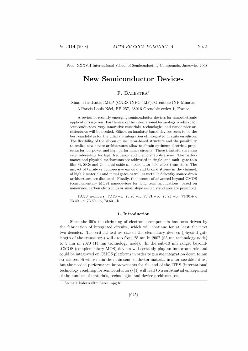
Virtual substrate development allows strained Ge layers to be created forp-channel operation, where the hole mobility can exceed the electron mobility insilicon. Relaxed buffers have been produced using a terrace grading approach withterminating layers having x = 80%, yet still retaining a good TDD significantlybelow 106 cm−2 and no pile up of dislocations (Fig. 1).
Reduction of the SiGe buffer layer thickness is also of great importance in or-der to reduce self-heating effects due in particular to the poor thermal conductivityof the SiGe layer compared with Si [4]. Therefore, further developments enabledthin VSs (< 300 nm thick) to be produced by RP-CVD (Reduced-Pressure Chem-ical Vapor Deposition) with p-channel devices fabricated having a 150 nm gate
New Semiconductor Devices 947
Fig. 1. Relaxed buffer layer of Si0.2Ge0.8 on Si(001), after etching to reveal threading
defects (seen as pits) with density below 106 cm−2.
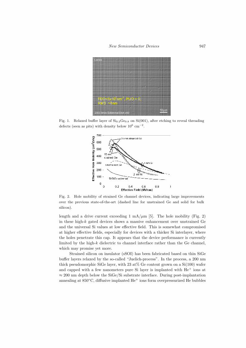
Fig. 2. Hole mobility of strained Ge channel devices, indicating large improvements
over the previous state-of-the-art (dashed line for unstrained Ge and solid for bulk
silicon).
length and a drive current exceeding 1 mA/µm [5]. The hole mobility (Fig. 2)in these high-k gated devices shows a massive enhancement over unstrained Geand the universal Si values at low effective field. This is somewhat compromisedat higher effective fields, especially for devices with a thicker Si interlayer, wherethe holes penetrate this cap. It appears that the device performance is currentlylimited by the high-k dielectric to channel interface rather than the Ge channel,which may promise yet more.
Strained silicon on insulator (sSOI) has been fabricated based on thin SiGebuffer layers relaxed by the so-called “Juelich-process”. In the process, a 200 nmthick pseudomorphic SiGe layer, with 23 at% Ge content grown on a Si(100) waferand capped with a few nanometers pure Si layer is implanted with He+ ions at≈ 200 nm depth below the SiGe/Si substrate interface. During post-implantationannealing at 850C, diffusive implanted He+ ions form overpressurized He bubbles
948 F. Balestra
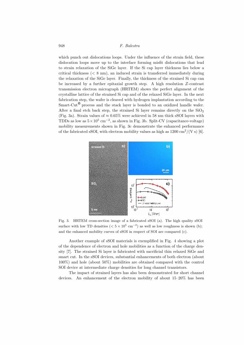
which punch out dislocations loops. Under the influence of the strain field, thesedislocation loops move up to the interface forming misfit dislocations that leadto strain relaxation of the SiGe layer. If the Si cap layer thickness lies below acritical thickness (< 8 nm), an induced strain is transferred immediately duringthe relaxation of the SiGe layer. Finally, the thickness of the strained Si cap canbe increased by a further epitaxial growth step. A high resolution Z-contrasttransmission electron micrograph (HRTEM) shows the perfect alignment of thecrystalline lattice of the strained Si cap and of the relaxed SiGe layer. In the nextfabrication step, the wafer is cleaved with hydrogen implantation according to theSmart-CutR process and the stack layer is bonded to an oxidized handle wafer.After a final etch back step, the strained Si layer remains directly on the SiO2
(Fig. 3a). Strain values of ≈ 0.65% were achieved in 58 nm thick sSOI layers withTDDs as low as 5×105 cm−2, as shown in Fig. 3b. Split-CV (capacitance-voltage)mobility measurements shown in Fig. 3c demonstrate the enhanced performanceof the fabricated sSOI, with electron mobility values as high as 1200 cm2/(V s) [6].
Fig. 3. HRTEM cross-section image of a fabricated sSOI (a). The high quality sSOI
surface with low TD densities (< 5× 105 cm−2) as well as low roughness is shown (b);
and the enhanced mobility curves of sSOI in respect of SOI are compared (c).
Another example of sSOI materials is exemplified in Fig. 4 showing a plotof the dependence of electron and hole mobilities as a function of the charge den-sity [7]. The strained Si layer is fabricated with sacrificial thin relaxed SiGe andsmart cut. In the sSOI devices, substantial enhancements of both electron (about100%) and hole (about 50%) mobilities are obtained compared with the controlSOI device at intermediate charge densities for long channel transistors.
The impact of strained layers has also been demonstrated for short channeldevices. An enhancement of the electron mobility of about 15–20% has been

New Semiconductor Devices 949
Fig. 4. Effective mobility comparison between sSOI and SOI MOSFETs.
obtained for 70 nm technology SGOI MOSFETs (strained Si on SiGe on insulator)together with superior short channel control. A significant increase in the drivingcurrent has been shown for these advanced devices (Fig. 5) [8, 9].
Fig. 5. Id−Vd of 70 nm MOSFETs (W = 1 µm).
The impact of the percentage of Ge is shown in Fig. 6. The electron mo-bilities are represented for various Ge content of the SiGe layer and different Sifilm thicknesses. The electron mobility enhancement is maximum for 30% of Gedue to the increase in alloy scattering and/or surface roughness, and the hole mo-bility continuously increases with Ge up to 50% [9]. It is also worth noting thatthe enhancement of carrier mobility is reduced in thinner strained Si films dueto interface states and fixed charges induced by the diffusion of Ge atoms to theinterfaces.
Figure 7a,b shows Idsat and Gmsat as a function of channel length for SGOIand SOI MOSFETs. An enhancement of Id is outlined down to sub-50 nm tran-sistors for SGOI, but the difference diminishes at smaller channel length due in

950 F. Balestra
Fig. 6. Eeff dependence of electron mobility enhancement as a function of Ge content
and film thickness.
Fig. 7. Comparison of Idsat and Gmsat at a constant gate overdrive.
particular to larger self-heating (SH) in SiGe than in Si. This SH effect in SGOIdegrades Gmsat, which is more sensitive to SH than Id. Therefore the transconduc-tance appears degraded in SGOI as compared to SOI but after correction of theself-heating a similar increase is obtained for Id and Gm in the SGOI structure [10].
The HOI structure (strained Si/strained SiGe/ strained Si heterostructure oninsulator) presents also substantial electron and hole mobility enhancements [11].In particular, hole mobilities are very high for thin Si cap layer (enhancement ofabout 100%) compared with the universal SOI mobility and are also significantlylarger that the best SSDOI mobility (strained Si directly on insulator) due to thecompressively strained buried SiGe channel (Fig. 8).
Uniaxial strain engineering is also useful for mobility enhancement for Sifilm thickness in the sub-10 nm range [12], which will be needed for the ultimateintegration of nanoMOSFETs. A similar enhancement of electron mobility in3.5 nm SOI devices under biaxial and uniaxial tensile strain has been obtained.

New Semiconductor Devices 951
Fig. 8. Mobility enhancement in HOI compared with the best SSDOI curve relative to
the “universal” SOI mobility.
Fig. 9. Electron mobility in 2.3 nm ultra-thin-body MOSFET under 〈110〉 uniaxial
strain.
The electron mobility is also enhanced in 2.3 nm Si layer under uniaxial tensilestrain (Fig. 9), and the hole mobility increases in 2.5 nm film under uniaxialcompressive strain.
The influence of surface roughness (SR) in ultra-thin films is very important.Figure 10 shows the SR limited hole mobility as a function of body thickness for Si(SOI) and Ge (GOI) channels. The variation of hole mobility is outlined for varioussurface orientations [13], which is also a major parameter for the optimization ofthe MOSFET electrical properties.
Figure 11 represents electron mobilities in FinFETs with various fin ori-entations. An improvement of electron mobility is observed for 〈100〉 and anenhancement of hole mobility has also been shown for 〈110〉 orientation [14].
Process-induced strain is also interesting to boost semiconductor device per-formance. It has recently been shown that the use of a metal gate (TiN) caninduce significant compressive stress along the channel direction. This stress is

952 F. Balestra
Fig. 10. Simulated surface roughness limited hole mobility for Si and Ge with various
orientations.
Fig. 11. Electron mobility of FinFETs (Fin Field-Effect Transistors) with 〈100〉 and
〈110〉 fin orientation. Tox = 2 nm, 4.5× 1013 cm−2 channel implantation.
increased as the gate length decreases. This phenomenon progressively degradeselectron mobility while hole transport is improved. Similar behaviors are obtainedin single and double gate SOI devices, and the use of 〈110〉 channel orientation isthe most favorable in terms of electrical performance [15].
2.2. Metallic Schottky source/drain MOSFETs
As CMOS technology is entering the decananometer era, the contact resis-tance associated with the silicide/silicon interface is identified as one of the biggestchallenges to solve in order to preserve current drive capabilities. In that context,source/drain (S/D) engineering takes an increasing importance in the developmentof leading edge CMOS generations because of the increasing impact of S/D seriesresistances on transistor performance. In order to further pursue down-scalingof MOSFETs in the sub-32 nm range of gate lengths, novel devices that hierar-chically combine alternative materials as well new architecture concepts such asmulti-gated channel have been proposed. Considering that the aforementioned
New Semiconductor Devices 953
innovations are expected to contribute to a higher current drive at shallower junc-tion depth and reduced silicide thickness, extremely severe constraints are placedon the junction and contact technologies.
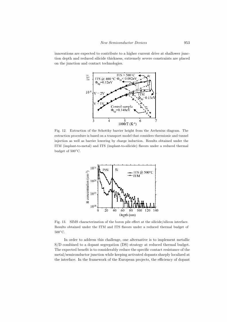
Fig. 12. Extraction of the Schottky barrier height from the Arrhenius diagram. The
extraction procedure is based on a transport model that considers thermionic and tunnel
injection as well as barrier lowering by charge induction. Results obtained under the
ITM (implant-to-metal) and ITS (implant-to-silicide) flavors under a reduced thermal
budget of 500C.
Fig. 13. SIMS characterization of the boron pile effect at the silicide/silicon interface.
Results obtained under the ITM and ITS flavors under a reduced thermal budget of
500C.
In order to address this challenge, one alternative is to implement metallicS/D combined to a dopant segregation (DS) strategy at reduced thermal budget.The expected benefit is to considerably reduce the specific contact resistance of themetal/semiconductor junction while keeping activated dopants sharply localized atthe interface. In the framework of the European projects, the efficiency of dopant

954 F. Balestra
Fig. 14. Ion−Ioff state-of-the-art of S/D p-MOSFET on SOI substrate indicating that
boron DS p-MOSFETs is leading the SOA of both SB and conventional unstrained
thin-film SOI technologies.
segregated Schottky contacts has been demonstrated [16–18]. The implementationof dopant segregated contact is illustrated by considering the following three dis-tinctive features: (i) implant-to-silicide (ITS), (ii) band-edge low Schottky barrier(SB) to holes (PtSi) and (iii) thermal budget limited to 500C. It has been shownthat the ITS scheme coupled to BF+
2 provides a sub-100 meV barrier (Fig. 12) con-sistently with the boron pile-up observed at the PtSi/Si interface (Fig. 13). A newstate-of-the-art current drive performance has been established for SB-MOSFETsat 25 nm of gate length: Ion of 530 µA/µm at Vg = Vd = −1.1 V. Figure 14also demonstrates that metallic S/D competes with best unstrained channel SOIp-FET technologies. A record RF performance for a 30 nm p-type unstrainedthin-film fully depleted SOI SB MOSFET has been demonstrated with a fT of180 GHz [16]. The effect of strained semiconductor is also thoroughly studied:carrier injection from a metallic junction should benefit from band splitting andfrom the corresponding Schottky barrier height reduction.
2.3. High-k materialsIn the search for new insulator materials for the 22 nm CMOS node and
beyond, the dielectric constant itself is not sufficient as a physical quantity tofulfill for technical device specification. The ultimate device property in this con-text is the gate leakage current for a given “equivalent oxide thickness” (EOT)needed to achieve a high enough capacitive coupling between transistor gate andchannel. For a perfectly amorphous or monocrystalline insulator material, thisquantity is limited by tunneling. Thus, the combination of dielectric constant, k,and the energy barrier height governed by the offset, E, between the energy bandsof the insulator and silicon is crucial from this viewpoint. For electron leakage,the relation between these two quantities can roughly be described as hyperbolicsuch that E × k = CE , where CE is a constant, determined by the leakage and

New Semiconductor Devices 955
gate coupling properties required for a certain technology node [19]. For the “lowstandby power” (LSTP) 22 nm bulk CMOS node, CE ≈ 70 eV, while the corre-sponding requirement for SOI technology (fully depleted double gate) can be setto CE ≈ 30 eV. These relations are summarized in Fig. 15.
Fig. 15. Energy offset values between the conduction bands of various dielectrics and
silicon versus dielectric constant. The upper shadowed area is a border for the 22 nm
LSTP bulk CMOS node. The lower shadowed area represents the corresponding border
for FD DG SOI technology.
Fig. 16. Density of interface states as a function of free energy gap position related to
the silicon valence band. The peaks for all three materials, HfO2, Gd2O3 and LaSiOx
are in the range 0.2–0.3 eV, common for the Pb peak.
For Gd2O3, prepared by two different methods, atomic layer deposition(ALD) and MBE, respectively, for LaSiOx prepared by evaporation and for HfO2
prepared by sputtering, studies have been performed in order to understand thebehavior of interface states at the high-k/silicon interface. We have found thatfor all these materials, the interface states behave similar to Pb centers existing
956 F. Balestra
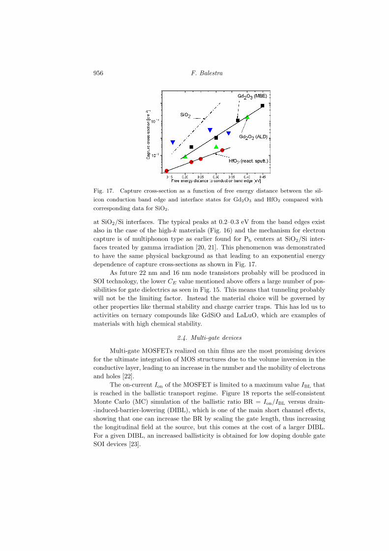
Fig. 17. Capture cross-section as a function of free energy distance between the sil-
icon conduction band edge and interface states for Gd2O3 and HfO2 compared with
corresponding data for SiO2.
at SiO2/Si interfaces. The typical peaks at 0.2–0.3 eV from the band edges existalso in the case of the high-k materials (Fig. 16) and the mechanism for electroncapture is of multiphonon type as earlier found for Pb centers at SiO2/Si inter-faces treated by gamma irradiation [20, 21]. This phenomenon was demonstratedto have the same physical background as that leading to an exponential energydependence of capture cross-sections as shown in Fig. 17.
As future 22 nm and 16 nm node transistors probably will be produced inSOI technology, the lower CE value mentioned above offers a large number of pos-sibilities for gate dielectrics as seen in Fig. 15. This means that tunneling probablywill not be the limiting factor. Instead the material choice will be governed byother properties like thermal stability and charge carrier traps. This has led us toactivities on ternary compounds like GdSiO and LaLuO, which are examples ofmaterials with high chemical stability.
2.4. Multi-gate devices
Multi-gate MOSFETs realized on thin films are the most promising devicesfor the ultimate integration of MOS structures due to the volume inversion in theconductive layer, leading to an increase in the number and the mobility of electronsand holes [22].
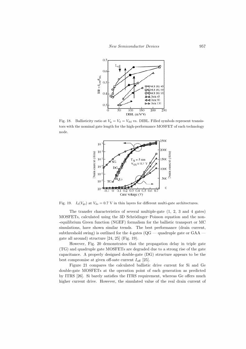
The on-current Ion of the MOSFET is limited to a maximum value IBL thatis reached in the ballistic transport regime. Figure 18 reports the self-consistentMonte Carlo (MC) simulation of the ballistic ratio BR = Ion/IBL versus drain--induced-barrier-lowering (DIBL), which is one of the main short channel effects,showing that one can increase the BR by scaling the gate length, thus increasingthe longitudinal field at the source, but this comes at the cost of a larger DIBL.For a given DIBL, an increased ballisticity is obtained for low doping double gateSOI devices [23].
New Semiconductor Devices 957
Fig. 18. Ballisticity ratio at Vg = Vd = Vdd vs. DIBL. Filled symbols represent transis-
tors with the nominal gate length for the high-performance MOSFET of each technology
node.
Fig. 19. Id(Vgs) at Vds = 0.7 V in thin layers for different multi-gate architectures.
The transfer characteristics of several multiple-gate (1, 2, 3 and 4 gates)MOSFETs, calculated using the 3D Schrodinger–Poisson equation and the non--equilibrium Green function (NGEF) formalism for the ballistic transport or MCsimulations, have shown similar trends. The best performance (drain current,subthreshold swing) is outlined for the 4-gates (QG — quadruple gate or GAA —gate all around) structure [24, 25] (Fig. 19).
However, Fig. 20 demonstrates that the propagation delay in triple gate(TG) and quadruple gate MOSFETs are degraded due to a strong rise of the gatecapacitance. A properly designed double-gate (DG) structure appears to be thebest compromise at given off-sate current Ioff [25].
Figure 21 compares the calculated ballistic drive current for Si and Gedouble-gate MOSFETs at the operation point of each generation as predictedby ITRS [26]. Si barely satisfies the ITRS requirement, whereas Ge offers muchhigher current drive. However, the simulated value of the real drain current of

958 F. Balestra
Fig. 20. Propagation delay versus Ioff for single-gate and multi-gate SOI devices.
Fig. 21. Ballistic drive current for different technology nodes for SOI and GOI devices.
Fig. 22. Evolution of Ioff with misalignment (experimental and simulations results,
Vd = 1.2 V). Single gate FD results are represented in dashed line.

New Semiconductor Devices 959
Fig. 23. Ion, subthreshold (Isub) and gate direct tunneling (Igdt) currents as a function
of gate underlap.
Fig. 24. Schematic diagram of MBCFET on SOI.
2G SOI transistors is not able to satisfy the ITRS objectives, even for intrinsicdevices without parasitic S/D resistances. 2G GOI MOSFETs are able to pro-vide the needed current drive, but parasitic resistances drastically affect the draincurrent (not shown here).
For a double gate device, the impact of a gate misalignment on the draincurrent is important. The impact of a gate misalignment is significant for Ion
in 2G MOSFETs [27]. A large back gate (BG) shift reduces the saturation cur-rent compared to the aligned case, whereas a slight BG shift towards the sourceincreases Ion. This is due to a lower source access resistance. In terms of shortchannel effects, aligned transistors exhibit the best control while highly misalignedMOSFETs operate like single gate ones. Ioff is much more influenced by the mis-alignment than Ion due to a degradation of the electrostatic control (Fig. 22).The oversized transistor shows attractive static performance (right hand side ofFig. 22) and a larger tolerance to misalignment but the dynamic performance israpidly degraded as the overlap length increases.
In decananometer MOSFETs, gate underlap is also a promising solution inorder to reduce the DIBL effect. Figure 23 presents the variations of the drivingcurrent Ion, the subthreshold current Isub and the gate direct tunneling currentIgdt versus gate underlap [28]. The on-current is almost not affected by the gate

960 F. Balestra
underlap whereas the leakage currents are substantially reduced due to a decreasein DIBL and drain to gate tunneling current. A reduction of the effective gate ca-pacitance Cg for larger underlap values at Ion has also been shown. This reductionof Cg leads to a decrease in the propagation delay and power.
In order to reach very high performance devices at the end of theroadmap, multi-bridge-channel MOSFETs (MBCFET) present very high drivingcurrents larger than those of GAA devices and exceeding the ITRS requirements(Fig. 24) [29].
3. Beyond-CMOS
The background of the activities investigated in this field is concentrated onfuture emerging nanodevices because the CMOS roadmap predicts downscalinglimits and the end of classical and non-classical CMOS in the first 2 decades ofthe current century. New devices and architectures are thus required, but a lot ofphysical phenomena and alternative fabrication approaches which could be usefulfor new devices are not completely understood. Investigations are pursued to over-come the limitations and to ensure reliable achievement in future nanoelectronics.
The objectives are to explore the horizon beyond CMOS, or beyond Moore,by following closely the emerging nano-sciences and -technologies for alternativesilicon-based memory/logic devices.
3.1. Nanowires and carbon electronics
It has been shown previously that multi-gate architectures based on theconcept of volume inversion are very promising in order to overcome the numberof challenges for CMOS integration (short channel effects, driving current, etc.)down to decananometer gate length devices [22]. Gate-all-around semiconduc-tors nanowires (NW) can be seen as the ultimate integration of these innovativenanodevices and present very interesting properties.
Fig. 25. Electron density per unit length for various devices (FinFET, nanowires and
carbon-nanotube FETs). 65 nm technology node data (EOT = 0.9 nm, tsi = 5 nm).

New Semiconductor Devices 961
Fig. 26. Id(Vg) characteristics calculated for Si, Ge and GaAs gate-all-around
nanowires oriented along the [100] direction, with 4 nm wire diameter and 9 nm gate
length; 1 nm gate oxide; Vds = 0.4 V.
Fig. 27. Id(Vd) characteristics calculated for n- and p-types Si nanowire FETs with
four different channel orientations; 3 nm wire diameter, 8 nm gate length; 1 nm gate
oxide; Vds = 0.4 V.
Therefore, it is interesting to compare the electrical properties of multi-gate devices with cylindrical and rectangular nanowires and with gate-all-aroundcarbon nanotubes — CNT-FET. It is shown that the CNT-FET exhibits superiorperformance (Fig. 25) due to electron charge confinement at the surface of thenanotube, whereas in the Si-based nanowires the charge confinement at the centerof the wire is responsible for an additional depletion capacitance in series withthe oxide capacitance, which reduces the overall effectiveness of the gate [30].However, the integration of these CNT-FETs on CMOS platform present manychallenges that will be discussed below. On the other hand, it is worth notingthat the performances of GAA nanowires, which could be realized using top-downtechnological processes, are larger than those obtained in FinFETs.

962 F. Balestra
Fig. 28. Id(Vd) characteristics calculated for Si and Ge nanowires FETs with [110]
channel orientation; 3 nm wire diameter, 8 nm gate length; 1 nm gate oxide; Vds = 0.4 V.
Very small nanowires, with diameters in the sub-10 nm range, are comparedfor various channel materials and orientations using 3D quantum-mechanical sim-ulations in pure ballistic regime [31]. Figure 26 shows the transfer current–voltagecharacteristics for a 9 nm long nanowire with a 4 nm diameter, the gate workfunc-tions being adjusted to provide identical off-current. The Si and Ge nanowiresprovide similar on-current, whereas the GaAs nanowire suffers from a high source-to-drain tunneling in the subthreshold region leading to a smaller Ion/Ioff ratio.
In Fig. 27, the output Id−Vd characteristics are calculated using full-bandsimulations with a ballistic FET model for Si n- and p-type nanowire FETs withfour different channel orientations, 8 nm gate length and 3 nm wire diameter [32].Due to the behavior of the transport effective-mass and valley degeneracy, it isdemonstrated that [110] is the best orientation for n- and p-channels that offersthe highest Ion for the same off-current for this 3 nm wire diameter. For thisoptimum channel orientation, Ge nanowires lead to an increase in Id between30 and 40% for p- and n-type devices, respectively, compared to Si nanowires(Fig. 28).
The variation of the intrinsic device delay with the wire diameter is shown inFig. 29 for Si and Ge n- and p-type nanowires and various channel orientations [32].p-channel nanowires display a monotonically increasing speed with decreasing thewire diameter, while the performance of n-channel nanowires highly depends onwire orientation and material.
The combination of strain effects with these 1D structures can lead tovery high performance ICs for the end of the roadmap. Top-down bended gate-all-around nanowires have been fabricated in order to improve carrier mobilityand driving current [33]. A bending induced by thermal oxidation in suspendednanowires is shown in Fig. 30. A maximum tensile strain is obtained in the middleof the wire.
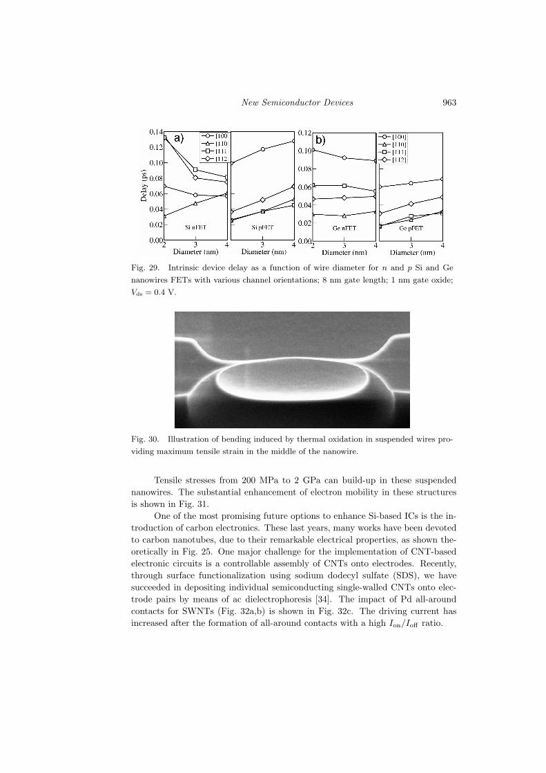
New Semiconductor Devices 963
Fig. 29. Intrinsic device delay as a function of wire diameter for n and p Si and Ge
nanowires FETs with various channel orientations; 8 nm gate length; 1 nm gate oxide;
Vds = 0.4 V.
Fig. 30. Illustration of bending induced by thermal oxidation in suspended wires pro-
viding maximum tensile strain in the middle of the nanowire.
Tensile stresses from 200 MPa to 2 GPa can build-up in these suspendednanowires. The substantial enhancement of electron mobility in these structuresis shown in Fig. 31.
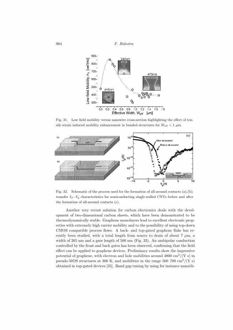
One of the most promising future options to enhance Si-based ICs is the in-troduction of carbon electronics. These last years, many works have been devotedto carbon nanotubes, due to their remarkable electrical properties, as shown the-oretically in Fig. 25. One major challenge for the implementation of CNT-basedelectronic circuits is a controllable assembly of CNTs onto electrodes. Recently,through surface functionalization using sodium dodecyl sulfate (SDS), we havesucceeded in depositing individual semiconducting single-walled CNTs onto elec-trode pairs by means of ac dielectrophoresis [34]. The impact of Pd all-aroundcontacts for SWNTs (Fig. 32a,b) is shown in Fig. 32c. The driving current hasincreased after the formation of all-around contacts with a high Ion/Ioff ratio.
964 F. Balestra
Fig. 31. Low field mobility versus nanowire cross-section highlighting the effect of ten-
sile strain induced mobility enhancement in bended structures for Weff < 1 µm.
Fig. 32. Schematic of the process used for the formation of all-around contacts (a),(b);
transfer Id−Vg characteristics for semiconducting single-walled CNTs before and after
the formation of all-around contacts (c).
Another very recent solution for carbon electronics deals with the devel-opment of two-dimensional carbon sheets, which have been demonstrated to bethermodynamically stable. Graphene monolayers lead to excellent electronic prop-erties with extremely high carrier mobility and to the possibility of using top-downCMOS compatible process flows. A back- and top-gated graphene flake has re-cently been studied, with a total length from source to drain of about 7 µm, awidth of 265 nm and a gate length of 500 nm (Fig. 33). An ambipolar conductioncontrolled by the front and back gates has been observed, confirming that the fieldeffect can be applied to graphene devices. Preliminary results show the impressivepotential of graphene, with electron and hole mobilities around 4800 cm2/(V s) inpseudo-MOS structures at 300 K, and mobilities in the range 500–700 cm2/(V s)obtained in top-gated devices [35]. Band gap tuning by using for instance nanorib-

New Semiconductor Devices 965
Fig. 33. Schematic of graphene field-effect devices.
bons or bilayer graphene could be used to improve gate modulation and devicecharacteristics.
3.2. Templated self-organization
The main objectives of this work are the defined positioning of self-organizednanostructures, their functionalization, and the demonstration of routes towardtheir implementation on fabrication schemes for integrated devices.
The crucial step in exact positioning is given by the nucleation on patternedtemplates where the pattern is larger than the self-organized nanostructures. Thematerial systems for starting are dots from silicon (Si)/oxide and SiGe/Si andcatalyst/Si wires. The extension to other material systems is planned for cou-pled self-organization sequences (e.g. self-organized contact to self-organized dot,phase change structure on top of a transistor array). Functionalization is directedtoward enhanced transport, carrier injection and storage, tunneling for novel writeerase strategies, optoelectronic emission/absorption for optical interconnect. De-vice fabrication routes are demonstrated for nanodevices using templated self--organization. The economic prospects of the implementation of templated self--organization in the manufacturing process are assessed. A breakthrough for uti-lization of templated self-organization is envisioned which should pave a way totechnical and economic benefits connected with a simpler manufacturing scheme.
We describe here recent progress of templated self-organization on nano-structure formation by different techniques and demonstration of functionalization.
Quantum dots (QDs) implementation in devices allows the improvement ofdevice performances and the design of new device structures, however, it requiresthe control of QD locations. In order to define dot positions, molecular beamepitaxy growth of Ge in oxide window is employed. Besides its compatibility withSi technology, this positioning process is able to produce dislocation-free single Gedots in selected areas. Figure 34 gives an example of a single Ge dot positioned inoxide window.
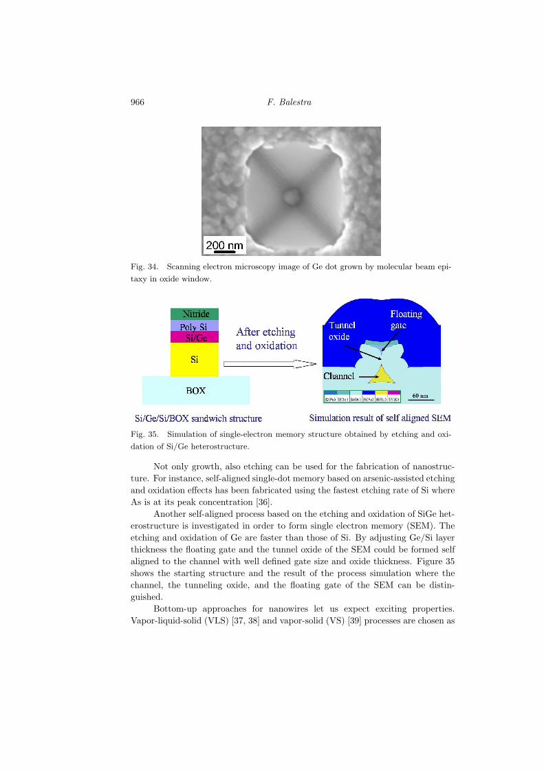
966 F. Balestra
Fig. 34. Scanning electron microscopy image of Ge dot grown by molecular beam epi-
taxy in oxide window.
Fig. 35. Simulation of single-electron memory structure obtained by etching and oxi-
dation of Si/Ge heterostructure.
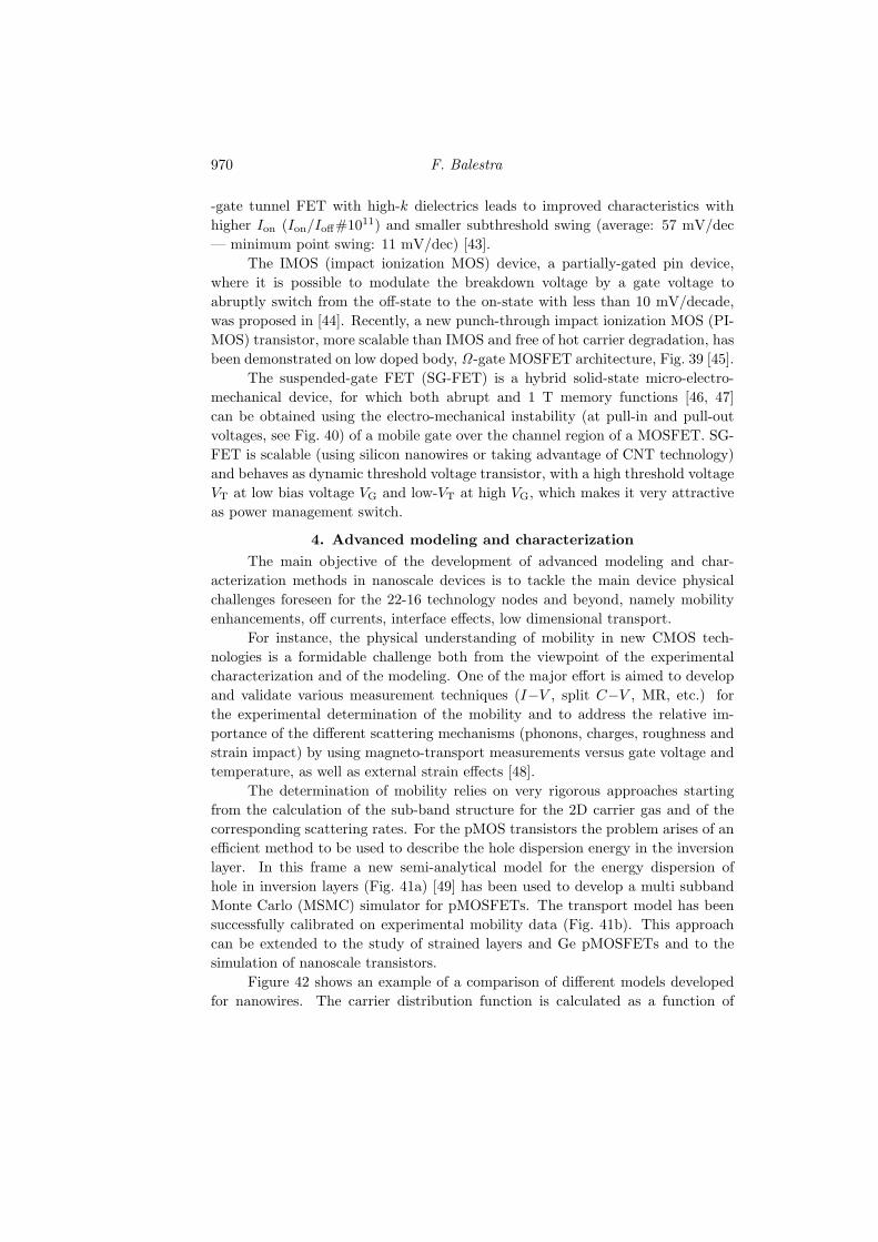
Not only growth, also etching can be used for the fabrication of nanostruc-ture. For instance, self-aligned single-dot memory based on arsenic-assisted etchingand oxidation effects has been fabricated using the fastest etching rate of Si whereAs is at its peak concentration [36].
Another self-aligned process based on the etching and oxidation of SiGe het-erostructure is investigated in order to form single electron memory (SEM). Theetching and oxidation of Ge are faster than those of Si. By adjusting Ge/Si layerthickness the floating gate and the tunnel oxide of the SEM could be formed selfaligned to the channel with well defined gate size and oxide thickness. Figure 35shows the starting structure and the result of the process simulation where thechannel, the tunneling oxide, and the floating gate of the SEM can be distin-guished.
Bottom-up approaches for nanowires let us expect exciting properties.Vapor-liquid-solid (VLS) [37, 38] and vapor-solid (VS) [39] processes are chosen as

New Semiconductor Devices 967
Fig. 36. Scanning electron microscopy of: (a) Si NWs grown with Au as catalyst,
(b) Si NWs grown with PtSi as catalyst, and (c) 45 nm diameter connected NW.
(d) I(V ) characteristic of a NW FET.
vehicles to generate Si quantum wires. The VLS method uses liquid Au-Si dropletas a catalyst to initiate the growth by chemical vapor deposition (CVD). A two-step process has been recently proposed to obtain very small diameter nanowires(< 10 nm). Firstly, the growth of large diameter NWs is realized. Depending onthe growth conditions, gold nanoparticles could remain at the sidewalls of the wiredirectly after the growth. Then, experimental parameters are changed in order togrow the nanometric diameter NWs at the sidewalls, i.e. a nanotree with nano-metric branches is formed [37, 38]. Nevertheless, gold particles introduce deeplevels in silicon which is detrimental to device functionality.
Unlike Au-Si liquid droplet, the solid Pt-Si used as catalyst for VS pro-cess is fully CMOS-compatible, the nanowire growth direction being random(Fig. 36a,b) [39].
Nanostructure functionalization is important as it is the first step towardtheir implementation in device structures. Functionalization of Si nanowire isachieved through its implementation in FET device (Fig. 36c). The influence ofthe gate on the NWs conduction and a drain current modulation of about 4 ordersof magnitude have been observed (Fig. 36d).
Other bottom-up processes have been developed for the CVD growth of Sinanowires and carbon nanotubes with CMOS-compatible catalysts (Al for Si NWsand Ge for CNTs [40]).

968 F. Balestra
These results show a rapid progress in self-organized formation of nanostruc-tures and a successful demonstration of Si nanowire functionalization.
3.3. Small slope switches
Even though the aggressive scaling will continue to play an important rolein the future nanoelectronics, new technology drivers, such as ultra-low power andnew functionality will open alternative ways for future high performance systems.
Fig. 37. Comparison of Ioff/Ion transition in ideal, small slope and MOS switches.
Fig. 38. Effect of gate length scaling from 1 µm down to 10 nm on ID−VG and gm−VG
characteristics of high-k double-gate tunnel FET.
One interesting class of beyond CMOS devices are the small slope switches.A small slope electronic switch (Fig. 37) is defined here as a solid-state semi-conductor device showing a value of the subthreshold slope smaller than the60 mV/decade limit for a conventional MOSFET, set by the Boltzmann distri-bution at room temperature. The smaller the value of S, the more abrupt thetransition from the off- to the on-state and closer the switch to the ideal case.Benefits of small slope switches are the ultra-low standby power due to a verylow Ioff but also the high-speed potential and dynamic power savings, since less

New Semiconductor Devices 969
Fig. 39. Abrupt switching in PIMOS due to impact ionization and bipolar onset.
Fig. 40. Abrupt switching in SG-MOSFET due to electro-mechanical non-equilibrium
(pull-in effect).
power is drawn per transition when the subthreshold slope is more abrupt. De-velopment of small slope switches requires exploration of new physical principlesfor very abrupt off-on transition, such as: (i) impact ionization, (ii) band-to-bandtunneling and (iii) electro-mechanical instability, solutions that are the candidatesanalyzed in this work. It is worth noting that all these small slope device ar-chitectures can be implemented as extensions of advanced silicon CMOS or byhybridization of silicon CMOS with other compatible technologies (SiGe, CNT,nano-electro-mechanical).
The tunnel FET [41–43] is a gated p−i−n diode with a gate over the intrinsicregion; it exploits the gate controlled electron tunneling from the valence band ofthe p-region to the conduction band of the i-region for reversed biases, resultingin very abrupt off-on transition. They have been reported on Si, III–V and CNTalternatives. High-k tunnel FETs can be scaled to shorter lengths before impor-tant characteristics such as transconductance, Ion/Ioff , and subthreshold swing aredegraded (Fig. 38). Optimized silicon body of 7–8 nm (for Lg = 50 nm) in double-
970 F. Balestra
-gate tunnel FET with high-k dielectrics leads to improved characteristics withhigher Ion (Ion/Ioff#1011) and smaller subthreshold swing (average: 57 mV/dec— minimum point swing: 11 mV/dec) [43].
The IMOS (impact ionization MOS) device, a partially-gated pin device,where it is possible to modulate the breakdown voltage by a gate voltage toabruptly switch from the off-state to the on-state with less than 10 mV/decade,was proposed in [44]. Recently, a new punch-through impact ionization MOS (PI-MOS) transistor, more scalable than IMOS and free of hot carrier degradation, hasbeen demonstrated on low doped body, Ω -gate MOSFET architecture, Fig. 39 [45].
The suspended-gate FET (SG-FET) is a hybrid solid-state micro-electro-mechanical device, for which both abrupt and 1 T memory functions [46, 47]can be obtained using the electro-mechanical instability (at pull-in and pull-outvoltages, see Fig. 40) of a mobile gate over the channel region of a MOSFET. SG-FET is scalable (using silicon nanowires or taking advantage of CNT technology)and behaves as dynamic threshold voltage transistor, with a high threshold voltageVT at low bias voltage VG and low-VT at high VG, which makes it very attractiveas power management switch.
4. Advanced modeling and characterizationThe main objective of the development of advanced modeling and char-
acterization methods in nanoscale devices is to tackle the main device physicalchallenges foreseen for the 22-16 technology nodes and beyond, namely mobilityenhancements, off currents, interface effects, low dimensional transport.
For instance, the physical understanding of mobility in new CMOS tech-nologies is a formidable challenge both from the viewpoint of the experimentalcharacterization and of the modeling. One of the major effort is aimed to developand validate various measurement techniques (I−V , split C−V , MR, etc.) forthe experimental determination of the mobility and to address the relative im-portance of the different scattering mechanisms (phonons, charges, roughness andstrain impact) by using magneto-transport measurements versus gate voltage andtemperature, as well as external strain effects [48].
The determination of mobility relies on very rigorous approaches startingfrom the calculation of the sub-band structure for the 2D carrier gas and of thecorresponding scattering rates. For the pMOS transistors the problem arises of anefficient method to be used to describe the hole dispersion energy in the inversionlayer. In this frame a new semi-analytical model for the energy dispersion ofhole in inversion layers (Fig. 41a) [49] has been used to develop a multi subbandMonte Carlo (MSMC) simulator for pMOSFETs. The transport model has beensuccessfully calibrated on experimental mobility data (Fig. 41b). This approachcan be extended to the study of strained layers and Ge pMOSFETs and to thesimulation of nanoscale transistors.
Figure 42 shows an example of a comparison of different models developedfor nanowires. The carrier distribution function is calculated as a function of

New Semiconductor Devices 971
Fig. 41. A new semi-analytical model for the energy dispersion of hole in inversion
layers has been used to develop a MSMC simulator for pMOSFETs (a). The transport
model has been successfully calibrated on experimental mobility data (b).
Fig. 42. Electron distribution function in a silicon nanowire as a function of energy,
velocity and position.
energy, velocity, and position, in a silicon nanowire using a deterministic solutionof the Boltzmann transport equation [50]. The calculated currents are shown inFig. 43. A significant drop of the driving current is obtained when the scatteringmechanisms are turned on compared to the ballistic case.
Figure 44 shows the study of the scattering from random dopants, which isa one of the biggest sources of variability, in n-channel nanowires using full self-consistent 3D Poisson-NEGF simulations [51]. Three cases are considered, twoof them have a discrete donor in the channel (DM: located at the middle of thecross-section, DA: donor located close to the SiO2 interface), the third one hasa discrete acceptor. The device without impurity is shown for comparison. Theoff-current is substantially increased in the cases of DM and DA due to two effects:the decrease in the gate barrier because of the presence of the attractive impurityand secondly the resonant tunneling structure induced by the impurity potential.

972 F. Balestra
Fig. 43. Turn-on characteristics of the cylindrical NWs with Lg = 10 nm.
Fig. 44. Transfer Id−Vg characteristics of n-channel nanowires for smooth and different
discrete dopants: donor (DM, DA) and acceptor cases.
The acceptor impurity device has the lowest current due to the repulsive barrierof the acceptor [52]. This theoretical analysis demonstrates the major importanceof the variability studies for the optimization of future semiconductor devices.
5. Conclusion
A number of recent advances obtained in the more Moore and beyond-CMOSactivities have been presented. These researches, mainly devoted to N+4 technol-ogy node and beyond for studying and validating new concepts, novel materialsand technologies, innovative device architectures, will enable us to overcome thenumber of research challenges of ultimate CMOS and post-CMOS nanodevices inorder to speed up technological innovation for the nanoelectronics of the next 2–3decades.
Acknowledgments
This work was partially supported by the European Networks of ExcellenceNANOSIL (FP7) and SINANO (FP6) devoted to silicon-based nanodevices.
New Semiconductor Devices 973
The authors would like to thank the very important contributions of all thePartners of these NoEs.
References
[1] ITRS Roadmap: http://www.itrs.net/.
[2] ENIAC Strategic Research Agenda: http://www.eniac.eu/web/SRA/local index.php.
[3] NANOSIL NoE web site: www.nanosil-noe.eu; SINANO NoE web site:
www.sinano.org.
[4] M. Myronov, Jap. J. Appl. Phys. 46, 721 (2007).
[5] G. Nicholas, IEEE Electron Dev. Lett. 28, 825 (2007).
[6] F. Driussi, D. Esseni, L. Selmi, M. Schmidt, M.C. Lemme, H. Kurz, D. Buca,
S. Mantl, M.Luysberg, R. Loo, D. Nguyen, M. Reiche, in: Proc. ESSDERC 2007,
p. 315.
[7] J.J. Lee, J.S. Maa, D.J. Tweet, in: Proc. IEEE Int. SOI Conf., 2004, p. 139.
[8] M. Sadaka, A.V.-Y. Thean, A. Barr, in Ref. [7] p. 209.
[9] T. Numata, T. Irisawa, T. Tezuka, in: Proc. IEDM’04, p. 177.
[10] J. Cai, K. Rim, A. Bryant, in Ref. [9], p. 165.
[11] I. Aberg, C.N. Chleirigh, O.O. Olubuyide, in Ref. [9], p. 173.
[12] K. Uchida, R. Zednik, C.H. Lu, in Ref. [9], p. 229.
[13] T. Low, in Ref. [9], p. 151.
[14] E. Landgraf, W. Rosner, M. Staedele, in: Proc. ULIS’2005, Bologna 2005, p. 15.
[15] T. Guillaume, M. Mouis, S. Maıtrejean, in [7], p. 42.
[16] G. Larrieu, E. Dubois, R. Valentin, N. Breil, F. Danneville, G. Dambrine,
J.C. Pesant, J.P. Raskin, in Ref. [9], p. 147.
[17] Z. Zhang, A. Qiu, R. Liu, M. Ostling, S.L. Zhang, Electron Dev. Lett. 28, 565
(2007).
[18] Q.T. Zhao, U. Breuer, E. Rije, S. Lenk, S. Mantl, Appl. Phys. Lett. 86, 062108
(2005).
[19] O. Engstrom, B. Raeissi, S. Hall, O. Buiu, M.C. Lemme, H.D.B. Gottlob,
P.K. Hurley, K. Cherkaoui, Solid State Electron. 51, 622 (2007).
[20] P.K. Hurley, K. Cherkaoui, E. O’Connor, M.C. Lemme, H.D.B. Gottlob,
M. Schmidt, S. Hall, Y. Lu, O. Buiu, B. Raeissi, J. Piscator, O. Engstrom,
S.B. Newcomb, J. Electrochem. Soc. 155, G13 (2008).
[21] B. Raeissi, J. Piscator, O. Engstrom, S. Hall, O. Buiu, M.C. Lemme, H.D.B.
Gottlob, P.K. Hurley, K. Cherkaoui, H.J. Osten, to be published in Solid State
Electron. 52, (2008).
[22] F. Balestra, S. Cristoloveanu, M. Benachir, IEEE Electron Dev. Lett. EDL-8,
410 (1987).
[23] S. Eminente, D. Esseni, P. Palestri, in Ref. [9], p. 609.
[24] M. Bescond, K. Nehari, J.L. Autran, in [9], p. 617.
[25] J. Saint-Martin, A. Bournel, P. Dollfus, in Ref. [14], p. 61.

974 F. Balestra
[26] A. Khakifirooz, O.M. Nayfeh, D.A. Antoniadis, in Ref. [7], p. 79.
[27] J. Widiez, F. Dauge, M. Vinet, in Ref. [7], p. 185.
[28] A. Bansal, B.C. Paul, K. Roy, in Ref. [7], p. 94.
[29] E.-J. Yoon, S.Y. Lee, S.M. Kim, in Ref. [9], p. 627.
[30] A. Marchi, E. Gnani, S. Reggiani, in Ref. [14], p. 99.
[31] M. Bescond, in Ref. [9].
[32] J. Wang, in Ref. [9].
[33] K.E. Moselund, in: Proc. IEDM’2007, p. 191.
[34] Z.-B. Zhang, J. Vac. Sci. Technol. B 24, (2006).
[35] M.C. Lemme, IEEE Electron. Dev. Lett. 28, 282 (2007).
[36] X. Tang, N. Reckinger, V. Bayot, C. Krzeminski, E. Dubois, A. Villaret,
D.-C. Bensahel, IEEE Trans. Nanotechnol. 5, 649 (2006).
[37] F. Dhalluin, P.J. Desre, M.I. Den Hertog, J.L. Rouviere, P. Ferret, P. Gentile,
T. Baron, J. Appl. Phys. 102, 094906 (2007).
[38] P. Gentile, T. David, F. Dhalluin, N. Pauc, M. Den Hertog, P. Ferret, T. Baron,
Nanotechnology 19, 125608 (2008).
[39] T. Baron, M. Gordon, F. Dhalluin, C. Ternon, P. Ferret, P. Gentile, Appl. Phys.
Lett. 89, 233111 (2006).
[40] T. Uchino, Appl. Phys. Lett. 86, 233110 (2005).
[41] K. Bhuwalka, Jap. J. Appl. Phys. 43, 4073 (2004).
[42] P.-F. Wang, Solid State Electron. 48, 2281 (2004).
[43] K. Boucart, A.M. Ionescu, IEEE Trans. Electron. Dev. 1725, (2007).
[44] K. Gopalakrishnan, in: Tech. Dig. IEDM’2002, p. 289.
[45] K.E. Moselund, in: Proc. ESSDERC 2007, p. 287.
[46] N. Abele, in: Tech. Dig. IEDM’2005, Late News, p. 479.
[47] N. Abele, in: Tech. Dig. IEDM’2006, p. 509.
[48] W. Chaisantikulwat, M. Mouis, G. Ghibaudo, C. Gallon, C. Fenouillet-Beranger,
D.K. Maude, T. Skotnicki, S. Cristoloveanu, Solid State Electron. 51, 1494 (2007).
[49] De Michielis, IEEE Trans. Electron. Dev. 54, 2164 (2007).
[50] M. Lenzi, in: Proc. ULIS’2007.
[51] A. Martinez, IEEE Trans. Electron Dev. 54, 2213 (2007).
[52] A. Martinez, J.R. Barker, A.R. Brown, N. Seoane, A. Asenov, to be presented at
SISPAD 2008.