new approaches to understand conductive and polar domain
TRANSCRIPT
HAL Id: tel-01412787https://tel.archives-ouvertes.fr/tel-01412787
Submitted on 8 Dec 2016
HAL is a multi-disciplinary open accessarchive for the deposit and dissemination of sci-entific research documents, whether they are pub-lished or not. The documents may come fromteaching and research institutions in France orabroad, or from public or private research centers.
L’archive ouverte pluridisciplinaire HAL, estdestinée au dépôt et à la diffusion de documentsscientifiques de niveau recherche, publiés ou non,émanant des établissements d’enseignement et derecherche français ou étrangers, des laboratoirespublics ou privés.
New approaches to understand conductive and polardomain walls by Raman spectroscopy and low energy
electron microscopyGuillaume F. Nataf
To cite this version:Guillaume F. Nataf. New approaches to understand conductive and polar domain walls by Ramanspectroscopy and low energy electron microscopy. Materials Science [cond-mat.mtrl-sci]. UniversitéParis-Saclay; Université du Luxembourg, 2016. English. �NNT : 2016SACLS436�. �tel-01412787�
NNT : 2016SACLS436
THESE DE DOCTORAT
DE
L’UNIVERSITE DU LUXEMBOURG
ET DE
L’UNIVERSITE PARIS-SACLAY
PREPAREE A L’UNIVERSITE PARIS-SUD
ÉCOLE DOCTORALE N°564
Physique en Île-de-France
Spécialité de doctorat : Physique
Par
M. Guillaume F. Nataf
New approaches to understand conductive and polar domain walls by Raman
spectroscopy and low energy electron microscopy
Thèse présentée et soutenue à Belvaux, le 5 octobre 2016 :
Composition du Jury :
M. Ludger Wirtz
M. Manfred Fiebig
Mme Nathalie Viart
Mme Agnès Barthélémy
M. Nicholas Barrett
M. Jens Kreisel
Professeur, Université du Luxembourg
Professeur, ETH Zürich
Professeure, Université de Strasbourg
Professeure, UMR CNRS/Thalès
Docteur, CEA Saclay
Professeur, LIST & Université du Luxembourg
Président du Jury
Rapporteur
Rapporteur
Examinatrice
Co-directeur de thèse
Co-directeur de thèse


iii
“No. Try not. Do... or do not. There is no try.”
“Ne! Nezkusíš! Uděláš to, nebo ne! Už žádné zkusit!”
- Jedi Master Yoda
iv
Acknowledgements
Je tiens tout d’abord à remercier les membres du jury qui ont accepté d’évaluer mon travail,
et en particulier mes rapporteurs Manfred Fiebig et Nathalie Viart. Merci aussi à Agnès
Barthélémy, examinatrice et Ludger Wirtz, président du jury. C’est un honneur de voir mon
travail jugé par eux ; leurs commentaires et questions m’ont indéniablement permis d’améliorer
ma compréhension des différents phénomènes présentés. Je suis par ailleurs heureux de
constater que la parité homme/femme était (presque) respectée dans mon jury.
Presque, car je remercie aussi chaleureusement mes deux directeurs de thèse, Jens Kreisel
et Nick Barrett. Chacun à leur manière ils m’ont permis de mener à bien ma thèse. Merci à Jens
pour sa confiance au quotidien et la liberté de travail qu’il m’a accordée. J’estime aujourd’hui la
chance que j’ai eu d’explorer un sujet aussi riche et original que celui qu’il m’a confié. Merci à
Nick pour son regard critique et son investissement quotidien qui m’ont notamment permis de
travailler à plusieurs reprises en synchrotron et de participer à la conférence LEEM-PEEM 10. Je
remercie évidemment Mael Guennou. Si officiellement il n’était pas co-encadrant, c’est pourtant
avec lui que j’ai travaillé au jour le jour. Nos nombreuses discussions ont rapidement dépassé le
cadre purement scientifique pour s’étendre à des échanges sur nos points faibles et points forts
respectifs. J’ai énormément appris grâce à lui et je garde en mémoire tous ses conseils.
Je dois beaucoup aux membres du CEA Saclay. Merci en particulier à Claire Mathieu qui a été
présente dans les moments importants. C’est grâce à elle et à Christophe Lubin que j’ai pu
effectuer des mesures PEEM. Le LEEM n’aurait pas été le même sans le travail quotidien de
Dominique Martinotti. Merci aussi à Ludovic Tortech et Cindy Rountree pour les mesures AFM.
Je dois évidemment beaucoup aux membres du Luxembourg Institute of Science and Technology
(et auparavant du CRP Gabriel Lippmann). Les mesures diélectriques et leur analyse ont été
possibles grâce à Torsten Granzow. Je souhaite aussi remercier Patrick Grysan avec qui j’ai
effectué de nombreuses mesures AFM/PFM. J’adresse un merci tout particulier à Nathalie Valle
(je sais qu’un jour le SIMS nous donnera la réponse). Je remercie enfin Pascal, Antoine, Bruno,
Stéphanie, Céline, Didier, Yves, Guillaume, Kevin, Petru, Bianca Rita, César, Naoufal, Jean-Seb,
Damien, Anaïs, Samir, Brahim, Jean-Nicolas, Gilles, Jorge, Manu, … pour l’aide qu’ils m’ont
apportée ou leurs mots gentils au détour d’un café (ou plutôt d’un verre d’eau). Merci aussi à
Servane avec qui j’ai eu la chance d’effectuer de nombreux footing.
J’ai l’occasion plus loin dans ce manuscrit de remercier quelques-uns des collaborateurs avec
qui j’ai interagi pour mon sujet de thèse. J’ai aussi eu la chance de mener des collaborations sur

v
d’autres sujets et je tiens donc à remercier : Pascal Ruello, Brahim Dkhil, Jan Lagerwall, Ingrid
Cañero-Infante, Bénédicte Warot-Fonrose, Joël Douin, Antoni Planes, Stéphane Fusil, Pierre
Eymeric-Janolin, Slavomír Nemšák et Michael Carpenter. Je souhaite adresser un remerciement
particulier à Ekhard Salje avec qui j’ai la chance de travailler régulièrement depuis 5 ans.
Un grand merci à tout le personnel de l’administration. Travailler au LIST serait bien terne
sans la bonne humeur quotidienne de Corinne ! Je remercie aussi Myriam Pannetier-Lecoeur
pour avoir suivi de près ma thèse. Je remercie tout particulièrement Gilles Montambaux qui a
toujours été à l’écoute et disponible pour signer les nombreux documents administratifs de
l’école doctorale.
J’ai évidemment une pensée pour tous les autres stagiaires, thésards ou post-docs qui ont
croisé ma route et sans qui la vie aurait été bien triste : Sara, Jelle, Quentin, Maxime, Qirong,
Ibrahima, Johanna, Daniel, Olivier, Nadège, Raquel, Dana, Hervé, Nicolas, Gaëlle, Charlotte,
Daniele, Romain, Hongjian, Peng, Simon, Carlos, Shankari, Alexander, Jonathan, Olga, Sunil,
Nohora, Alex, Serena, Mouss, ... Je remercie particulièrement David pour m’avoir fais découvrir
la culture belge (surtout les frites !). Un grand merci à tous ceux qui jouaient au foot le mercredi
soir, et en particulier à Vincent. Bien entendu, je remercie Mads avec qui j’espère pouvoir
travailler encore dans le futur.
J’ai aussi un immense merci à adresser à tous mes amis, à Grenoble, à Paris (à Grignon pour
être précis) et ailleurs : Julie, Ophélie, Laure, Anaïs, Olivier, Marvin, Elise, Marion, Myke, Justine,
Kevin, Taia, Yann, Florian, Hadrien, Hélène, ... J’ai chéri chaque instant en votre présence. Je
tiens à remercier mes colocataires avec qui j’ai partagé de nombreux moments et repas :
Quentin, Jean-Marc, Océane, Cyril, Vaiva, Damien, Vincenzo, Karine, Joshua et Céline.
Merci à Blandine. Merci à Aurore.
Enfin, une pensée me vient pour ma famille qui a été présente pendant ces 3 années et qui,
je le sais, sera toujours là quand j’en aurai besoin.

vi

vii
Contents
General introduction ............................................................................................. 1
I. Domains and domain walls ................................................................................. 3
1. Ferroic materials and domain structures ....................................................................... 4
1.1. Ferroic phase transitions............................................................................................. 4
1.2. Ferroelastics: spontaneous strain ............................................................................... 6
1.3. Ferroelectrics: spontaneous polarization ................................................................... 6
1.4. Ferroelectric hysteresis loop ....................................................................................... 6
1.5. Screening of ferroelectric surfaces ............................................................................. 8
2. Ferroelectric and ferroelastic domain walls ...................................................... 10
2.1. Classical approach: domain walls as interfaces ........................................................ 10
2.1.1. Types of ferroelectric domain walls ....................................................................... 10
2.1.2. Neutral and charged ferroelectric domain walls ................................................... 11
2.1.3. Mechanical compatibility at ferroelastic domain walls ......................................... 12
2.1.4. Optical identification of domain walls ................................................................... 13
2.1.5. Domain wall thickness ........................................................................................... 15
2.2. Renewed interest: domain wall engineering ............................................................ 18
2.2.1. Conductive domain walls in ferroelectrics ............................................................. 18
2.2.2. Polar domain walls in ferroelastics ........................................................................ 21
3. Summary ......................................................................................................... 27
II. Methods .......................................................................................................... 29
1. Raman spectroscopy ........................................................................................ 30
1.1. Harmonic theory of crystal vibrations ...................................................................... 30
1.2. LO-TO splitting .......................................................................................................... 31
1.3. Interaction of light and vibrational modes ............................................................... 32
1.4. Selection rules ........................................................................................................... 34
1.5. Experimental setup ................................................................................................... 35
1.6. Principal Component Analysis ................................................................................... 36
2. Low-energy electron microscopy...................................................................... 41
2.1. Experimental setup ................................................................................................... 41
2.2. MEM-LEEM transition ............................................................................................... 42
2.3. Imaging physical topography .................................................................................... 44
2.4. Imaging charged surfaces ......................................................................................... 44
3. Other techniques ............................................................................................. 46
3.1. Dielectric spectroscopy ............................................................................................. 46
3.2. Resonant piezoelectric spectroscopy ....................................................................... 48

viii
III. Interaction between defects and domain walls in lithium niobate ................... 51
1. Lithium niobate ................................................................................................ 52
1.1. General properties ................................................................................................... 52
1.2. Intrinsic and extrinsic defects ................................................................................... 53
1.3. Polaronic states ........................................................................................................ 54
1.4. Domain structure ...................................................................................................... 56
2. Stabilization of electronic defects at domain walls as seen by dielectric
spectroscopy ............................................................................................................. 58
2.1. State of the art .......................................................................................................... 58
2.2. Experimental conditions ........................................................................................... 59
2.3. Monodomain samples .............................................................................................. 59
2.4. Periodically poled lithium niobate ............................................................................ 61
3. Bent domain walls as seen by transmission electron microscopy ...................... 65
4. Stabilization of polar defect structures at domain walls as seen by Raman
spectroscopy ............................................................................................................. 67
4.1. State of the art .......................................................................................................... 67
4.2. Experimental conditions ........................................................................................... 69
4.3. Principal Component Analysis .................................................................................. 70
4.4. Absence of signature of momentum absorption by domain walls .......................... 75
4.5. Influence of magnesium concentration ................................................................... 76
4.6. Influence of the internal field ................................................................................... 77
4.7. Raman-signatures at domain walls .......................................................................... 79
4.8. Discussion ................................................................................................................. 80
4.9. Influence of UV light ................................................................................................. 81
5. Summary and conclusions on the conductive domain walls .............................. 83
IV. Low-energy electron imaging of domain walls in lithium niobate ..................... 85
1. State of the art ................................................................................................. 86
2. Surface preparation ......................................................................................... 87
3. Characterization of the surface by piezoelectric force microscopy ..................... 87
4. Evaluation of the surface potential ................................................................... 89
4.1. MEM-LEEM transition .............................................................................................. 89
4.2. Influence of screening .............................................................................................. 92
5. Out-of-focus imaging of charged regions .......................................................... 93
6. Signature of domain walls ................................................................................ 96
7. Conclusion ....................................................................................................... 99

ix
V. Polar domain walls in calcium titanate .......................................................... 101
1. Calcium titanate ............................................................................................ 102
1.1. Structure ................................................................................................................. 102
1.2. Spontaneous strain tensor ...................................................................................... 103
1.3. Orientation of ferroelastic domain walls ................................................................ 104
1.4. Twin angle ............................................................................................................... 105
2. Piezoelectric response as seen by resonant piezoelectric spectroscopy ........... 106
2.1. Experimental conditions ......................................................................................... 106
2.2. Natural frequencies of the sample ......................................................................... 107
2.3. Oscillation of polar domain walls ............................................................................ 108
3. Surface investigation by low energy electron microscopy ............................... 110
3.1. Surface preparation ................................................................................................ 110
3.2. Surface orientation and stoichiometry ................................................................... 110
3.3. Domain surface topography ................................................................................... 112
3.4. Electron imaging of domain walls ........................................................................... 113
3.6. Under and over-focusing ........................................................................................ 116
3.7. Electron injection and polarity screening ............................................................... 119
3.8. Reversibility of polarity screening ........................................................................... 121
3.9. Discussion ................................................................................................................ 122
4. Conclusions on polar domain walls ................................................................ 124
Conclusion ........................................................................................................ 125
Summary ........................................................................................................................ 125
Perspectives ................................................................................................................... 127
References ........................................................................................................ 128
Collaborations ................................................................................................... 136
Publications ...................................................................................................... 137
Résumé en français ........................................................................................... 138


1
General introduction
Following the discovery of ferroelectric perovskites[1], a tremendous amount of work was
performed to understand the nucleation and growth of ferroelectric domains[2–4]. One key
parameter lies within the kinetics of the domain walls: when does a domain wall start moving?
How fast does it move? Answers to these questions were obtained with experimental setups
using liquid electrodes to apply an external electric field to the sample while taking optical
images. They led to a comprehensive picture of the velocity of the domain walls under an
electric field[5].
The interest for domain walls was renewed later when it was realized that the irreversible
displacement of ferroelectric-ferroelastic domain walls increases the piezoelectric coefficients of
ceramics, even at low driving electric fields. For example, in barium titanate, up to 35% of the
total longitudinal piezoelectric coefficient d33 comes from domain wall motion[6]. Since this
motion depends on the microstructure of the ceramic, the influence of the crystal structure, the
crystallographic orientation and the domain size were investigated. Several strategies were then
developed to engineer the ferroelectric domain structure in order to enhance the piezoelectric
response of ceramics[7]. This field has been coined “domain engineering”.
The examples mentioned above utilize the properties of the ferroelectric domains solely and
domain walls appear only as interfaces that can influence the domain structure. However, the
discovery of superconductivity localized at the ferroelastic domain walls of tungsten oxide
(WO3‐x) has opened a new path of research[8]. For the first time, domain walls were not simply
seen as interfaces between domains but as distinct elements with their own functional
properties. Almost ten years later, conduction at ferroelectric domain walls was reported in the
insulator bismuth ferrite (BiFeO3)[9] and led to the research of conductive domain walls in other
materials[10–16]. Conduction under illumination[13] and free-electron gas[14] localized at domain
walls were part of the intriguing discoveries. In the meantime, experimental evidences of
polarity at ferroelastic domain walls in non-polar materials were given[17–19] and the idea to
switch the polarization of the domain walls germinated[20].
The overall frame of applications arising from this research has been thought as “domain
walls nanoelectronics”[21] or “domain boundary engineering”[22] where the domain walls carry
information and act as memory devices. Three characteristics guarantee the interest of
ferroelectric and ferroelastic domain walls for device applications: they are thin[21], their position
can be controlled[23,24] and they exhibit functional properties[21,22].

2 General introduction
However, some fundamental questions remain: what are the mechanisms behind the
conduction of ferroelectric domain walls? In particular, what is the role of defects? What are the
characteristics of the polarization in the ferroelastic domain walls? Is it possible to control this
polarization?
Answering these questions requires studying the electrical properties of domain walls and
therefore experimental techniques sensitive to structural changes, defects, polarization and also
techniques with a high spatial resolution. This thesis presents measurements performed on the
bulk with dielectric spectroscopy and resonant piezoelectric spectroscopy, at a microscopic scale
with Raman micro-spectroscopy, and at a sub-micrometric scale with low energy electron
microscopy. Two materials have been investigated: the ferroelectric lithium niobate, known to
present conductive domain walls under illumination[13,25], and the ferroelastic calcium titanate,
where polar domain walls have been characterized[18,19].
This manuscript is organized as follows. In Chapter I, the basics of the physics of ferroic
domains and domain walls are presented, with a focus on the functional properties of domain
walls. The main methods used in this thesis are detailed in Chapter II. In Chapter III, we
investigate the influence of ferroelectric domain walls on the dielectric response of single
crystals of lithium niobate and report resonance features related to the presence of defect-
decorated domain walls. The evolution of the Raman modes at domain walls for a large series of
magnesium-doped lithium niobate samples sheds more light on the interaction between polar
defects and domain walls. In Chapter IV, we analyze contrast formation in low energy electron
microscopy applied to domains and domain walls in lithium niobate. In particular, we show that
the intensity profile at domain walls provides experimental evidence for a local, stray electric
field. Chapter V is dedicated to the investigations of the electric response of the polarization in
the domain walls of calcium titanate by resonant piezoelectric spectroscopy and low energy
electron microscopy and gives a way toward the usability of polar domain walls.
3
I. Domains and domain walls
4 I. Domains and domain walls
1. Ferroic materials and domain structures
Ferroic materials display a spontaneous symmetry breaking and posses an order parameter,
such as spontaneous strain, spontaneous polarization, spontaneous magnetization or
ferrotoroidic moment, that can point in two or more directions and be switched between them
by application of an external field[21]. Here, we define the ferroic materials through their phase
transitions and present the notions of ferroelectric hysteresis and surface screening.
1.1. Ferroic phase transitions
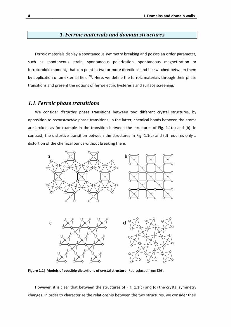
We consider distortive phase transitions between two different crystal structures, by
opposition to reconstructive phase transitions. In the latter, chemical bonds between the atoms
are broken, as for example in the transition between the structures of Fig. 1.1(a) and (b). In
contrast, the distortive transition between the structures in Fig. 1.1(c) and (d) requires only a
distortion of the chemical bonds without breaking them.
Figure 1.1| Models of possible distortions of crystal structure. Reproduced from [26].
However, it is clear that between the structures of Fig. 1.1(c) and (d) the crystal symmetry
changes. In order to characterize the relationship between the two structures, we consider their

1. Ferroic materials and domain structures 5
point groups, G and F. We define a high-symmetry phase (G) and a low-symmetry phase (F), such
that F is a proper subgroup of G (F ⊂ G). This leads to the definition of a ferroic phase transition:
if the point group of the low-symmetry phase (F) is a proper subgroup of the point group of the
high-symmetry phase (G), the transition from F to G is classified as ferroic[27].
During the transition, a new physical quantity appears in the ferroic phase, characteristic of
the symmetry change, called the order parameter. It is common to classify the order parameters
according to their behavior under space and time reversal, as shown in Fig. 1.2. This leads to the
definition of four order parameters (and the corresponding ferroic phases): spontaneous strain
(ferroelastic), spontaneous polarization (ferroelectric), spontaneous magnetization
(ferromagnetic) and ferrotoroidic moment (ferrotoroidic)[28].
Figure 1.2| Ferroic orders under the parity operations of space and time. Reproduced from [28].
It is important to notice that the order parameter can have different orientations in the
ferroic phase. When applying to the ferroic phase the symmetry operations of the high-
symmetry phase, the operations that are in common with those of the ferroic phase leave the
orientation unchanged while the others induce a change of orientation of the order parameter.
Since all the possible orientations are energetically equivalent, during the phase transition, the
ferroic phase spontaneously split in regions of different orientation of the order parameter. The
different regions of the crystals where the orientation of the order parameter is uniform are
called ferroic domains. They are related by the symmetry operations of the high-symmetry
phase which are not present in the ferroic phase.
6 I. Domains and domain walls
1.2. Ferroelastics: spontaneous strain
When the temperature of a crystal is changed, directionally dependent expansion and
contraction of different magnitudes occur. The relation between the induced strain and the
change in temperature is given by a symmetric second-rank tensor called the thermal expansion
tensor α[29]. The constraints on the non-zero components of the tensors and on the relations
between them are the same for crystallographic classes belonging to the same family. For
example, in all tetragonal systems αxx = αyy and αzz are two independent non-zero components
while off-diagonal coefficients are null.
A transition is called ferroelastic if it results in a low-symmetry phase in which the thermal
expansion tensor changes the number of its independent components with respect to those in
the high-symmetry phase. Given that this tensor is characteristic of a crystal family, the phase
transition is said to be ferroelastic if the high-symmetry phase and the low-symmetry phase
belong to different crystal families[26].
During a ferroelastic phase transition, the shape and size of the unit cell change. This change
can be expressed as a spontaneous strain exerted on the high-symmetry phase. The
spontaneous strain is therefore an order parameter of a ferroelastic material.
1.3. Ferroelectrics: spontaneous polarization
When the temperature T of a crystal is changed, the charge density at the surface can
change: this is the pyroelectric effect. The components of the pyroelectric coefficent are:
where is the electric polarization. The pyroelectric coefficient is non-zero only in polar
crystals[29].
A phase transition is ferroelectric if it results in a lower symmetry phase for which the
pyroelectric coefficient acquires new components which where zero, by symmetry, in the high-
symmetry phase[26].
The spontaneous polarization is the order parameter of a ferroelectric material.
1.4. Ferroelectric hysteresis loop
A ferroelectric material is usually composed of randomly distributed ferroelectric domains
where the spontaneous polarization is uniform. Under application of a strong enough electric

1. Ferroic materials and domain structures 7
field, the direction of the polarization changes. This process, called poling, reorients the
polarization of the domains in directions allowed by the crystal symmetry and that lie as close as
possible to the direction of the electric field. The polarization reversal by an electric field is the
signature of a ferroelectric material and appears as a hysteresis loop[30].
A schematic of a hysteresis loop is shown in Fig. 1.3. We start from a random structure of
domains with an average polarization equal to zero (point A). An electric field is applied to
the ferroelectric material. Usually the field is applied along one of the polar axes. As the value of
the field is increased, above the coercive field value Ec, domains with an unfavorable direction of
polarization switch, leading to an abrupt increase of the polarization. Once the domains are all
aligned, a monodomain state is obtained, and the ferroelectric behaves as a normal linear
dielectric (points B). When the field is decreased to zero, some domains switch but the overall
polarization is non null. This is the remanent polarization Pr. A further increase of the field in the
negative direction leads to another monodomain state (point C). The spontaneous polarization
Ps can be estimated by taking the intercept of the polarization axis with the extrapolated linear
segment in the monodomain state, as shown in Fig. 1.3.
Figure 1.3| Ferroelectric hysteresis loop. Squares with blue and white regions represent schematically the
repartition of domains with two different polarization orientations. The arrows indicate the direction of
the polarization. The symbols are explained in the text. Adapted from [30].

8 I. Domains and domain walls
1.5. Screening of ferroelectric surfaces
As shown schematically in Fig. 1.4, in a ferroelectric material, the polar discontinuity at the
bulk-terminated surface gives rise to a net fixed surface charge defined by , where
is the
spontaneous polarization and is the surface normal. These charges induce an electric field,
called the depolarization field Ed, opposite to the spontaneous polarization. As in the case of a
two-plate capacitor, the depolarization field has an electrostatic energy proportional to the
square of the surface charge. A monodomain state is therefore unfavorable due to the high
depolarization field whereas if two domains of opposite polarizations are adjacent, the
depolarization fields compensate each other and reduce the total electrostatic energy. In
Fig. 1.4, we label “Pup” a domain that has a polarization pointing upward at the surface and
“Pdown” a domain that has a polarization in the opposite direction.
Figure 1.4| Schematic of a ferroelectric domain structure in thin film. Polarization (black arrows) gives
rise to a surface charge depicted by the plus and minus symbols. The depolarization field (Ed) induced by
the charges is drawn with a blue arrow.
The depolarization field can also be reduced by electric field arising from charges. Such
screening is (i) external if the charges arise from adsorbates and (ii) internal if the screening
charges arise from defects/doping.
In the case of free surfaces, external screening can be performed by the adsorption of
molecules, such as water. Kalinin et al. have quantified the amount of screening charges ςs with
respect to the polarization charges ςpol[31]. In Fig. 1.5, three cases are distinguished: the surface is
(a) unscreened ςs = 0, (b) partially screened ςpol > - ςs, and (c) completely screened ςpol = - ςs. The
unscreened case is energetically unfavourable. The partially screened is very often observed in
air[32,33] and may occur in ultra-high vacuum as well[34,35].

1. Ferroic materials and domain structures 9
Figure 1.5| Screening mechanisms. Schematics of polarization charges and screening charges for (a)
unscreened, (b) partially screened and (c) completely screened surfaces. In this schematic, polarization
charges and screening charges are depicted by the plus and minus symbols, respectively.
Internal screening is the charge compensation arising from defects in the material: vacancies
and dopants can lead to an excess of free charges in the sample that are available to screen the
polarization charges[36]. In order to be efficient, internal screening requires the migration of the
internal charges toward the surface. Therefore, it is more efficient when annealing the sample
since temperature increases the mobility of free charges and also of ions in the material[37].

10 I. Domains and domain walls
2. Ferroelectric and ferroelastic domain walls
The interfaces between ferroic domains are called domain walls. Here, we present criteria to
classify ferroelectric domain walls based on the profile of their order parameter or their
inclination with respect to the ferroelectric axis. Then, we explain how ferroelectric and
ferroelastic domain walls are observed by optical techniques. We also give estimations of their
thickness. Finally, we present two intriguing and specific properties of domain walls: conductivity
in ferroelectric domain walls and polarity in ferroelastic domain walls.
While these results are more general, most of the experiments described here have been
performed on perovskites structures, which have a chemical formula ABO3 where A and B are
cations.
2.1. Classical approach: domain walls as interfaces
2.1.1. Types of ferroelectric domain walls
In ferroelectric materials, due to the piezoelectric coupling between the ferroelectric
polarization and the strain, rotating the polarization away from the symmetry-allowed direction
is energetically costly. Thus a 180°-ferroelectric domain wall between a Pdown and a Pup domain
can be considered as Ising-like, i.e. with no-in plane polarization associated with polarization
rotation, as shown in Fig. 1.6(a)[38].
Figure 1.6| Different types of ferroelectric domain walls. (a) Ising type, (b) Néel type and (c) Bloch type.
Arrows represent the polarization. θN and θB are the maximum rotation angles of the polarization in the
plane and perpendicular to it, respectively. Adapted from [39].

2. Ferroelectric and ferroelastic domain walls 11
The typical profile of the polarization across a domain wall is derived from Landau theory as
a hyperbolic tangent:
where P is the amplitude of the polarization, P0 the equilibrium value of the polarization far from
the domain wall, xn the spatial coordinate perpendicular to the domain wall and 2W the domain
wall thickness[40].
Magnetic domain walls present other types of profiles. Indeed, in magnetism, the spin is
quantized and cannot change his magnitude across a domain wall. Instead, it rotates within the
plane of the domain wall (Néel walls) or perpendicular to it (Bloch walls)[41], as shown in
Fig. 1.6(b) and 1.6(c), respectively.
By analogy with magnetism, Bloch and Néel profiles have also been discussed for
ferroelectrics. Recent Density Functional Theory (DFT) calculations have shown that the
structure of 180°-ferroelectric domain walls can have a mixed Bloch-Néel-Ising character. For
example, minimization of the energy of a 180° domain walls in lithium niobate by DFT leads to
the maximum polarization components (Pn, Pt, Pz)max=(0.56, 1.99, 62.4) μC/cm2 where Pn and Pt
are the polarizations normal and transverse to the domain wall, respectively. Pn and Pt lead to
Néel (Fig. 1.6(b)) and Bloch-like (Fig. 1.6(c)) rotations by maximum rotation angles of θN = 0.55°
and θB = 1.52°[39], respectively.
2.1.2. Neutral and charged ferroelectric domain walls
A criterion to differentiate ferroelectric domain walls is their net charge. We illustrate this
criterion on the case of 180°-domain walls.
An ideal 180°-domain wall is perfectly aligned with the direction of the ferroelectric axis and
is therefore neutral (Fig. 1.7(a)). Fig. 1.7(b) shows the case where a head-to-head configuration
of the polarization leads to a maximum positive charge at domain wall. A tail-to-tail
configuration, as shown in Fig. 1.7(c) leads to a maximum negative charge at domain wall.
Fig. 1.7(d) illustrates one case of a domain wall slightly inclined with respect to the ferroelectric
axis, which has a partial positive charge.

12 I. Domains and domain walls
Figure 1.7| Charges at domain walls (side view). (a) Neutral, (b) charged head-to-head, (c) charged tail-
to-tail and (d) partially charged, inclined domain wall. Polarization is depicted by black arrows and domain
walls are indicated by black lines.
Domain walls can be classified by the angle between the polarization directions of the
neighboring domains. We discussed above the case of 180° domain walls, but other orientations
are possible, such as 109° and 71° domain walls in bismuth ferrite[42].
2.1.3. Mechanical compatibility at ferroelastic domain walls
The orientation of the ferroelastic domain walls is usually determined by the requirement of
mechanical compatibility between the two adjacent domains. Indeed, a randomly oriented
domain wall can induce a large increase of the elastic strain in the material. This is energetically
unfavorable.
Let the spontaneous strain in the adjacent domains A and B, be ε(A) and ε(B). Then, the
orientation of the domain wall is such that the transformation of any geometrical figure, which
lies in the plane of the domain wall, due to deformations ε(A) and ε(B), should be identical. This
domain wall is said to be stress-free, since no additional elastic strain is involved[26].
Mathematically, the condition is satisfied if any vector in the domain wall fulfills the
condition:
where εij(A) - εij(B) is a symmetric tensor with up to six independent components, xi and xj are
the components of the vector [43]. Sapriel solved Eq. 1.3 by considering the spontaneous strain
2. Ferroelectric and ferroelastic domain walls 13
tensors in all the possible orientation states of the domains, and obtained the complete set of
equations of the permissible domain walls for all ferroelastic transitions[43].
Some of the equations of the permissible domain walls are derived from symmetry
considerations only and have fixed orientations. This is the case for every mirror plane W which
transform domain A into domain B. The precise orientation of the other domain walls, labeled
W’, depends on the relative values of the coefficients of the spontaneous strain tensor[43].
2.1.4. Optical identification of domain walls
We will show in section 2.1.5 that ferroelectric and ferroelastic domain walls are of
nanometer scale thickness. This makes challenging the localization of domain walls in a sample.
At first sight, it requires experimental techniques with nanometric spatial resolutions such as
atomic force microscopy[44,45] or transmission electron microscopy[18,46]. However, optical
techniques, which have a spatial resolution restricted by the optical diffraction limit (about
0.5 μm at best), can still be used to localize domain walls.
Ferroelastic domains are visible with polarized light microscopy because the refractive index
ellipsoid depends on the macroscopic spontaneous strain. Therefore, ferroelastic domain walls
are easily localized and usually appear as small lines in an optical image[47]. However, non-
ferroelastic ferroelectric 180°-domains are not visible with an optical microscope because the
ellipsoid of the refractive indices is centrosymmetric. Therefore, other optical techniques, such
as second harmonic generation (SHG) and Raman spectroscopy, are used.
SHG is observed in non-centrosymmetric materials and depends on the second-order
electrical susceptibility. Due to the nonlinearity of the second-order electrical susceptibility, the
incident light of frequency w generates a nonlinear polarization wave in the material that
oscillates at twice the frequency (2w). This nonlinear polarization wave radiates light at 2w[48].
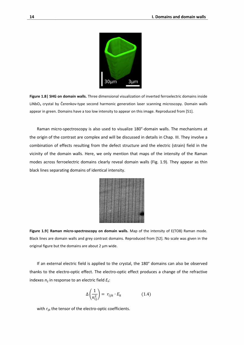
These photons form the SHG signal. At domain walls, the SHG signal is enhanced and is used to
perform 3D profiles[49–51], as shown in Fig. 1.8. This could be the signature of local strain that
could enhance the second-order electrical susceptibility at domain walls[51]. Since the spatial
resolution of SGH is restricted by the optical diffraction limit, the signal observed at domain
walls is always mixed with the signals of the surrounding domains.
14 I. Domains and domain walls
Figure 1.8| SHG on domain walls. Three dimensional visualization of inverted ferroelectric domains inside
LiNbO3 crystal by Čerenkov-type second harmonic generation laser scanning microscopy. Domain walls
appear in green. Domains have a too low intensity to appear on this image. Reproduced from [51].
Raman micro-spectroscopy is also used to visualize 180°-domain walls. The mechanisms at
the origin of the contrast are complex and will be discussed in details in Chap. III. They involve a
combination of effects resulting from the defect structure and the electric (strain) field in the
vicinity of the domain walls. Here, we only mention that maps of the intensity of the Raman
modes across ferroelectric domains clearly reveal domain walls (Fig. 1.9). They appear as thin
black lines separating domains of identical intensity.
Figure 1.9| Raman micro-spectroscopy on domain walls. Map of the intensity of E(TO8) Raman mode.
Black lines are domain walls and grey contrast domains. Reproduced from [52]. No scale was given in the
original figure but the domains are about 2 μm wide.
If an external electric field is applied to the crystal, the 180° domains can also be observed
thanks to the electro-optic effect. The electro-optic effect produces a change of the refractive
indexes nij in response to an electric field Ek:
with rijk the tensor of the electro-optic coefficients.

2. Ferroelectric and ferroelastic domain walls 15
In the case of an uniaxial ferroelectric, under an external electric field applied along the
polarization axis, the refractive index n0 changes to n0 + Δn0 in one domain and to n0 - Δn0 in the
other, as sketched in Fig. 1.10(a). Under an optical microscope, this difference leads to a
detectable light scattering, as shown in Fig. 1.10(b) where small hexagonal domains are
visible[53,54]. At domain walls, the index changes by 2Δn0. Domain walls appear then as thin dark
or white lines at the border of the hexagonal domains. If the sample contains polar defects, such
as in LiNbO3, the resulting internal electric field leads to a weak electro-effect and allows seeing
domain walls without applying an external electric field[55].
Figure 1.10| Electro-optic imaging. (a) Schematic showing the principle of electro-optic imaging at a 180°
domain wall. The refractive index increases when the applied electric field is antiparallel to the
spontaneous polarisation and decreases when it is parallel. (b) Polarized light microscopy image taken in
LiNbO3 under an external electric field of 21.6 kV/mm. Adapted from [53,54].
2.1.5. Domain wall thickness
The thickness of domain walls influences the physical properties of ferroelectric and
ferroelastic materials. For example, it has been shown that the domain wall thickness affects the
dielectric and piezoelectric responses of ferroelectric thin films[56]. It is also known that the width
of 180° stripe domains in thin films is proportional to the square root of the crystal thickness[57,58]
with a constant of proportionality expressed as a function of the domain walls thickness[59]. Thus,
a measurement of the domain wall thickness is important. Most of the studies so far have relied
on X-ray diffraction (XRD) or transmission electron microscopy (TEM).

16 I. Domains and domain walls
Figure 1.11| Diffraction on ferroelastic domains. (a) General principle of an X-Ray diffraction rocking
curve. In adjacent ferroelastic domains, atomic planes are not parallel. The crystal is rotated by an angle ω
about an axis perpendicular to the plane of incidence in order to bring each atomic plane into Bragg’s
condition. (b) A plot of integrated intensity as a function of angle ω, showing two peaks corresponding to
domains in a single crystal of LaAlO3. Adapted from [60].
In a ferroelastic material, the diffracting planes are not aligned along the same directions in
adjacent domains. For example, in Fig. 1.11(a), there is an angle of 0.25° between the crystal
planes of two adjacent domains. If the sample is aligned such that the first domain is in Bragg
condition, a rotation of ω = 0.25° about an axis perpendicular to the plane of incidence brings
the second domain into Bragg condition. A plot of diffracted intensity as a function of ω shows
two peaks corresponding to each domain (Fig. 1.11(b)).
In a ferroelastic sample with a high density of domains, a weak additional intensity is
observed between the two domain-related peaks, as shown in Fig. 1.12. This intensity arises
from the scattering of X-rays by atoms located in domain walls. The displacement of the atoms
in domain walls is modeled by a hyperbolic tangent and the corresponding scattered intensity as
a function of the incident angle is calculated for different thickness of the domain wall. A direct
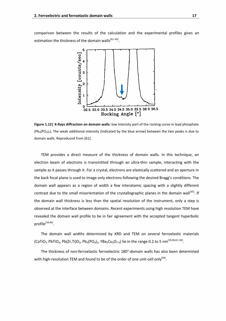
2. Ferroelectric and ferroelastic domain walls 17
comparison between the results of the calculation and the experimental profiles gives an
estimation the thickness of the domain walls[61–64].
Figure 1.12| X-Rays diffraction on domain walls: low intensity part of the rocking curve in lead phosphate
(Pb3(PO4)2). The weak additional intensity (indicated by the blue arrow) between the two peaks is due to
domain walls. Reproduced from [61].
TEM provides a direct measure of the thickness of domain walls. In this technique, an
electron beam of electrons is transmitted through an ultra-thin sample, interacting with the
sample as it passes through it. For a crystal, electrons are elastically scattered and an aperture in
the back focal plane is used to image only electrons following the desired Bragg’s conditions. The
domain wall appears as a region of width a few interatomic spacing with a slightly different
contrast due to the small misorientation of the crystallographic planes in the domain wall[65]. If
the domain wall thickness is less than the spatial resolution of the instrument, only a step is
observed at the interface between domains. Recent experiments using high resolution TEM have
revealed the domain wall profile to be in fair agreement with the accepted tangent hyperbolic
profile[18,46].
The domain wall widths determined by XRD and TEM on several ferroelastic materials
(CaTiO3, PbTiO3, Pb(Zr,Ti)O3, Pb3(PO4)2, YBa2Cu3O7-δ) lie in the range 0.2 to 5 nm[18,46,61–66].
The thickness of non-ferroelastic ferroelectric 180°-domain walls has also been determined
with high-resolution TEM and found to be of the order of one unit-cell only[66].
18 I. Domains and domain walls
2.2. Renewed interest: domain wall engineering
The discovery of superconductivity localized at the ferroelastic domain walls of tungsten
oxide has opened a new path of research[8]. For the first time, domain walls were seen as distinct
elements with their own functional properties. The overall framework of applications arising
from this research has been thought as “domain walls nanoelectronics”[21] or “domain boundary
engineering”[22]. Within this vision, domain walls carry information and act as memory devices.
In particular, Catalan et al. have proposed to reproduce the electronic logic circuits with domain
walls[21]. A first success was obtained with a ferroelectric domain-wall diode, which allows a
single direction of motion for all domain walls irrespective of their polarity, thanks to a thickness
gradient in the sample[67].
2.2.1. Conductive domain walls in ferroelectrics
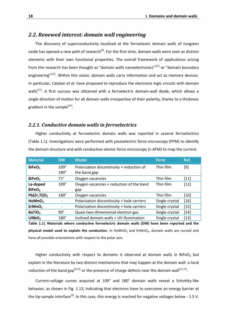
Higher conductivity at ferroelectric domain walls was reported in several ferroelectrics
(Table 1.1). Investigations were performed with piezoelectric force microscopy (PFM) to identify
the domain structure and with conductive-atomic force microscopy (c-AFM) to map the current.
Material DW Model Form Ref.
BiFeO3 109° 180°
Polarization discontinuity + reduction of the band gap
Thin film [9]
BiFeO3 71° Oxygen vacancies Thin film [11]
La-doped BiFeO3
109° Oxygen vacancies + reduction of the band gap
Thin film [12]
Pb(Zr,Ti)O3 180° Oxygen vacancies Thin film [10]
HoMnO3 - Polarization discontinuity + hole carriers Single crystal [16]
ErMnO3 - Polarization discontinuity + hole carriers Single crystal [15]
BaTiO3 90° Quasi-two-dimensional electron gas Single crystal [14]
LiNbO3 180° Inclined domain walls + UV illumination Single crystal [13] Table 1.1| Materials where conductive ferroelectric domain walls (DW) have been reported and the
physical model used to explain the conduction. In HoMnO3 and ErMnO3, domain walls are curved and
have all possible orientations with respect to the polar axis.
Higher conductivity with respect to domains is observed at domain walls in BiFeO3 but
explain in the literature by two distinct mechanisms that may happen at the domain wall: a local
reduction of the band gap[9,12] or the presence of charge defects near the domain wall[11,12].
Current-voltage curves acquired at 109° and 180° domain walls reveal a Schottky-like
behavior, as shown in Fig. 1.13, indicating that electrons have to overcome an energy barrier at
the tip-sample interface[9]. In this case, this energy is reached for negative voltages below - 1.5 V.
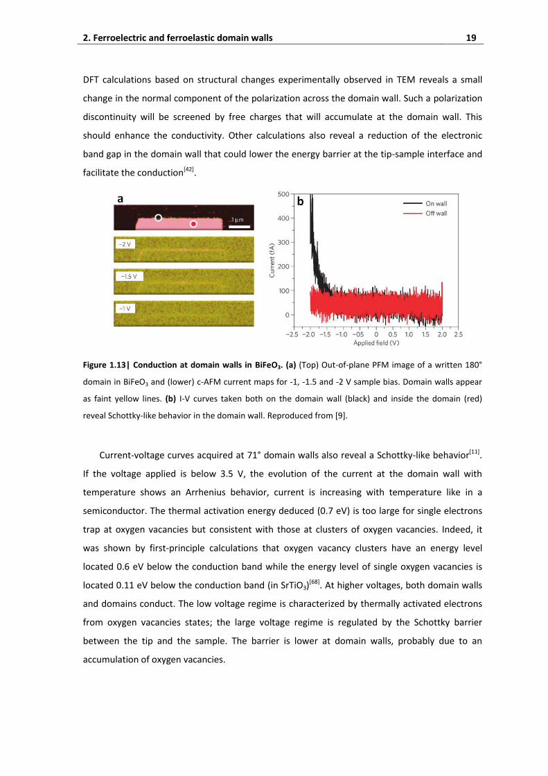
2. Ferroelectric and ferroelastic domain walls 19
DFT calculations based on structural changes experimentally observed in TEM reveals a small
change in the normal component of the polarization across the domain wall. Such a polarization
discontinuity will be screened by free charges that will accumulate at the domain wall. This
should enhance the conductivity. Other calculations also reveal a reduction of the electronic
band gap in the domain wall that could lower the energy barrier at the tip-sample interface and
facilitate the conduction[42].
Figure 1.13| Conduction at domain walls in BiFeO3. (a) (Top) Out-of-plane PFM image of a written 180°
domain in BiFeO3 and (lower) c-AFM current maps for -1, -1.5 and -2 V sample bias. Domain walls appear
as faint yellow lines. (b) I-V curves taken both on the domain wall (black) and inside the domain (red)
reveal Schottky-like behavior in the domain wall. Reproduced from [9].
Current-voltage curves acquired at 71° domain walls also reveal a Schottky-like behavior[11].
If the voltage applied is below 3.5 V, the evolution of the current at the domain wall with
temperature shows an Arrhenius behavior, current is increasing with temperature like in a
semiconductor. The thermal activation energy deduced (0.7 eV) is too large for single electrons
trap at oxygen vacancies but consistent with those at clusters of oxygen vacancies. Indeed, it
was shown by first-principle calculations that oxygen vacancy clusters have an energy level
located 0.6 eV below the conduction band while the energy level of single oxygen vacancies is
located 0.11 eV below the conduction band (in SrTiO3)[68]. At higher voltages, both domain walls
and domains conduct. The low voltage regime is characterized by thermally activated electrons
from oxygen vacancies states; the large voltage regime is regulated by the Schottky barrier
between the tip and the sample. The barrier is lower at domain walls, probably due to an
accumulation of oxygen vacancies.
20 I. Domains and domain walls
Conductivity arising from free electrons originating from oxygen vacancies is also reported at
109° domain walls in La-doped BiFeO3[12]. The main experimental result is that the current at
domain walls increases with increasing concentrations of oxygen vacancies.
Domain wall conductivity is observed along 180° domain walls in Pb(Zr,Ti)O3 and proposed
to be possible thanks to trap states, such as oxygen vacancies, within domain walls[10].
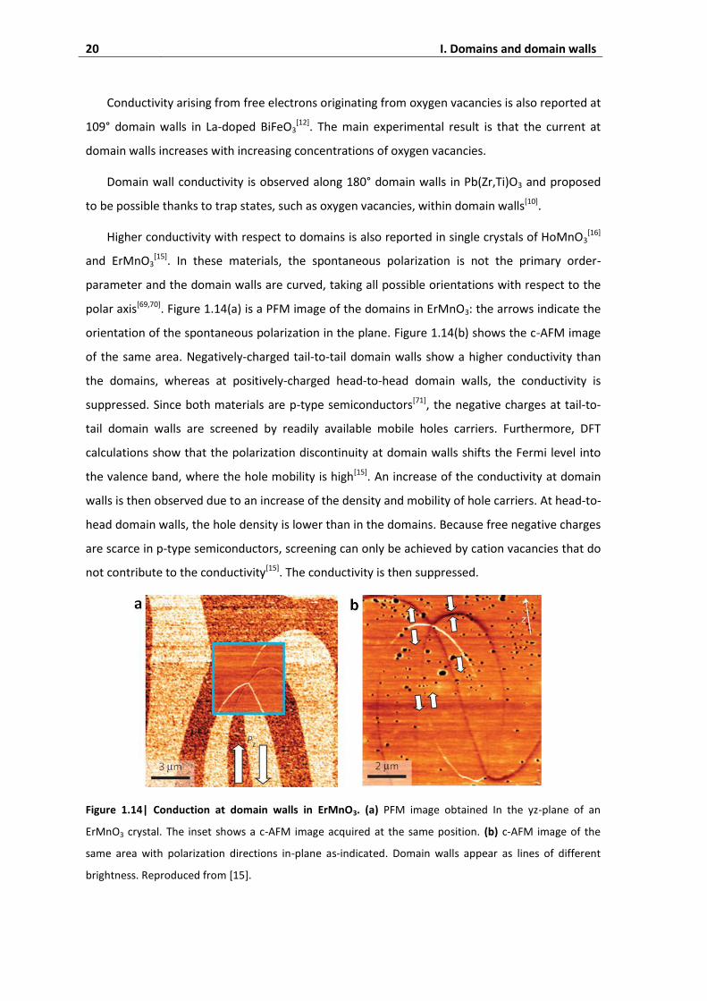
Higher conductivity with respect to domains is also reported in single crystals of HoMnO3[16]
and ErMnO3[15]. In these materials, the spontaneous polarization is not the primary order-
parameter and the domain walls are curved, taking all possible orientations with respect to the
polar axis[69,70]. Figure 1.14(a) is a PFM image of the domains in ErMnO3: the arrows indicate the
orientation of the spontaneous polarization in the plane. Figure 1.14(b) shows the c-AFM image
of the same area. Negatively-charged tail-to-tail domain walls show a higher conductivity than
the domains, whereas at positively-charged head-to-head domain walls, the conductivity is
suppressed. Since both materials are p-type semiconductors[71], the negative charges at tail-to-
tail domain walls are screened by readily available mobile holes carriers. Furthermore, DFT
calculations show that the polarization discontinuity at domain walls shifts the Fermi level into
the valence band, where the hole mobility is high[15]. An increase of the conductivity at domain
walls is then observed due to an increase of the density and mobility of hole carriers. At head-to-
head domain walls, the hole density is lower than in the domains. Because free negative charges
are scarce in p-type semiconductors, screening can only be achieved by cation vacancies that do
not contribute to the conductivity[15]. The conductivity is then suppressed.
Figure 1.14| Conduction at domain walls in ErMnO3. (a) PFM image obtained In the yz-plane of an
ErMnO3 crystal. The inset shows a c-AFM image acquired at the same position. (b) c-AFM image of the
same area with polarization directions in-plane as-indicated. Domain walls appear as lines of different
brightness. Reproduced from [15].
2. Ferroelectric and ferroelastic domain walls 21
A metallic-type giant domain wall conductivity (109 times higher than in the domains) is
observed at 90° head-to-head domain walls in BaTiO3. It is interpreted within the framework of a
quasi-two-dimensional electron gas[14].
Higher conductivity is reported at 180° domain walls in single crystals of LiNbO3 but it
requires illumination with UV light[13]. This measurement was performed with small diodes that
shined light on the sample during c-AFM imaging. The current is observed only under above-
band gap illumination. It is higher when domain walls are slightly inclined with respect to the
ferroelectric axis (angle < 0.25°). This inclination is controlled via doping with different
concentrations of magnesium and all inclined domain walls are positively charged in this case.
These positive carriers should increase the conductivity. UV-light seems to provide additional
charges by creation of electron-hole pairs.
2.2.2. Polar domain walls in ferroelastics
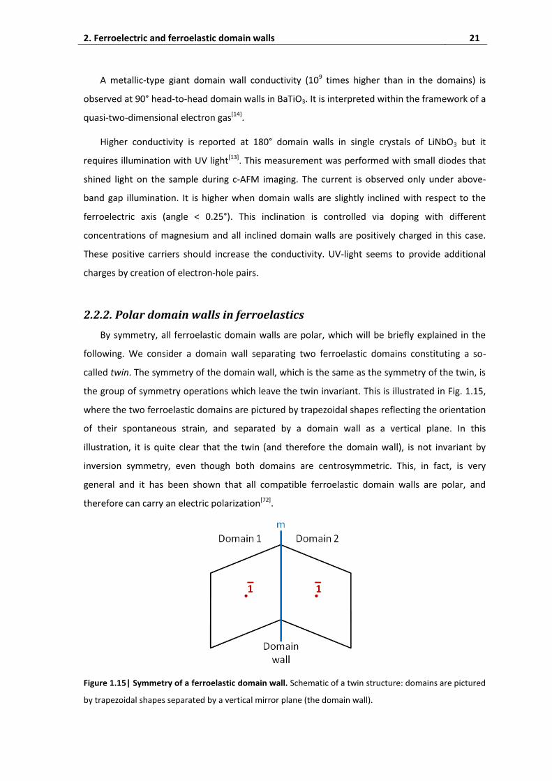
By symmetry, all ferroelastic domain walls are polar, which will be briefly explained in the
following. We consider a domain wall separating two ferroelastic domains constituting a so-
called twin. The symmetry of the domain wall, which is the same as the symmetry of the twin, is
the group of symmetry operations which leave the twin invariant. This is illustrated in Fig. 1.15,
where the two ferroelastic domains are pictured by trapezoidal shapes reflecting the orientation
of their spontaneous strain, and separated by a domain wall as a vertical plane. In this
illustration, it is quite clear that the twin (and therefore the domain wall), is not invariant by
inversion symmetry, even though both domains are centrosymmetric. This, in fact, is very
general and it has been shown that all compatible ferroelastic domain walls are polar, and
therefore can carry an electric polarization[72].
Figure 1.15| Symmetry of a ferroelastic domain wall. Schematic of a twin structure: domains are pictured
by trapezoidal shapes separated by a vertical mirror plane (the domain wall).
22 I. Domains and domain walls
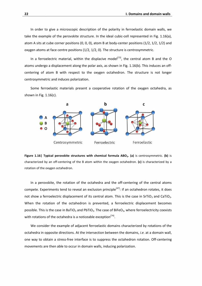
In order to give a microscopic description of the polarity in ferroelastic domain walls, we
take the example of the perovskite structure. In the ideal cubic-cell represented in Fig. 1.16(a),
atom A sits at cube corner positions (0, 0, 0), atom B at body-center positions (1/2, 1/2, 1/2) and
oxygen atoms at face centre positions (1/2, 1/2, 0). The structure is centrosymmetric.
In a ferroelectric material, within the displacive model[73], the central atom B and the O
atoms undergo a displacement along the polar axis, as shown in Fig. 1.16(b). This induces an off-
centering of atom B with respect to the oxygen octahedron. The structure is not longer
centrosymmetric and induces polarization.
Some ferroelastic materials present a cooperative rotation of the oxygen octahedra, as
shown in Fig. 1.16(c).
Figure 1.16| Typical perovskite structures with chemical formula ABO3. (a) is centrosymmetric. (b) is
characterized by an off-centering of the B atom within the oxygen octahedron. (c) is characterized by a
rotation of the oxygen octahedron.
In a perovskite, the rotation of the octahedra and the off-centering of the central atoms
compete. Experiments tend to reveal an exclusion principle[47]: if an octahedron rotates, it does
not show a ferroelectric displacement of its central atom. This is the case in SrTiO3 and CaTiO3.
When the rotation of the octahedron is prevented, a ferroelectric displacement becomes
possible. This is the case in BaTiO3 and PbTiO3. The case of BiFeO3, where ferroelectricity coexists
with rotations of the octahedra is a noticeable exception[74].
We consider the example of adjacent ferroelastic domains characterized by rotations of the
octahedra in opposite directions. At the intersection between the domains, i.e. at a domain wall,
one way to obtain a stress-free interface is to suppress the octahedron rotation. Off-centering
movements are then able to occur in domain walls, inducing polarization.

2. Ferroelectric and ferroelastic domain walls 23
This expectation is confirmed by computer simulations on CaTiO3[75]. Goncalves-Ferreira et
al. simulated a sample with two ferroelastic domain walls. Fig. 1.17(a) shows the oxygen
octahedra rotation across the domain walls. It follows the hyperbolic tangent profile expected
from Landau theory, with a domain wall thickness of 80 Å (consistent with the experimental
value[18]). At the centre of the domain walls, indicated by vertical lines, the rotation is
suppressed. Fig. 1.17(b) shows the off-centering of the central Ti atom with respect to the
oxygen octahedra, as a function of the angle of rotation Q (for sake of simplicity, only the
displacement along one direction is shown). Far from the domain wall, the rotation is large and
the off-center displacement is null. At the domain wall, the angle of rotation is null and the Ti
atom is slightly displaced: this implies a polar domain wall.
Figure 1.17| Competition between rotation of the octahedra and off-centering of Ti atoms. (a)
Octahedra rotation Q as a function of the position perpendicular to the domain wall. The dashed line is a
fit to the expected hyperbolic tangent profile. The vertical lines indicate the position of domain walls. (b)
Off-centering of Ti atoms along the x-coordinates within their corresponding O octahedron as a function
of the octahedral rotation Q. Reproduced from [75].
The first experimental evidence of polar domain walls in CaTiO3 was obtained by aberration-
corrected TEM[18]. Fig. 1.18(a) schematizes the domain wall geometry as imaged and Fig. 1.18(b)
shows the TEM image obtained with a spatial resolution of 0.8 Å. Ca atoms appear as black
features separated by Ti atoms. An angle of 181.2° (or equivalently 178.8°) is clearly identified
between the two domains.

24 I. Domains and domain walls
Figure 1.18| TEM experiment on polar domain walls in CaTiO3. (a) Schematic of a single domain wall,
indicated as standing dark grey plane, with the chosen (x, y, z) reference system for the definitions of the
measured displacements. (b) Amplitude of the reconstructed exit wave. The CaTiO3 crystal is imaged along
the [001] zone axis orientation, the (110) domain wall is indicated by the horizontal white line.
Reproduced from [18].
In order to determine the atomic positions, statistical parameter estimation theory was
used. The interatomic distances between neighboring Ca-Ca and Ti-Ti columns were then
calculated. It was found that the Ca-Ca distance is constant while the Ti-Ti distance changes near
domain walls. Therefore, the analysis was focused on the off-centering of the Ti atomic position
with respect to the neighboring four Ca atoms. Since these displacements were largely random
and small, they were averaged in planes perpendicular to the domain wall. Next, the results in
the planes above and below the domain wall were also averaged. The resulting displacements
are shown in Fig. 1.19(a). Perpendicular to the domain wall, Ti atoms are shifted by 3.1 pm in the
second closest layers pointing toward the twin wall (Fig. 1.19(b)). A larger displacement of 6.1
pm is measured parallel to the domain wall in the layer adjacent (Fig. 1.19(c)). It corresponds to
a polarization of 0.04-0.2 C/m2, comparable with for example the value of bulk spontaneous
polarization in the prototypical ferroelectric barium titanate, at room temperature.

2. Ferroelectric and ferroelastic domain walls 25
Figure 1.19| Atomic displacements at domain walls. (a) Phase of the reconstructed exit wave. Mean
displacements of the Ti atomic columns from the center of the four neighboring Ca atomic columns are
indicated by green arrows. The blue horizontal line shows the position of the domain wall. (b,c)
Displacements of Ti atomic columns in the x- and y-directions averaged along and in mirror operation with
respect to the domain wall together with their 90% confidence intervals. Reproduced from [18].
A second experimental evidence of polar domain walls has been provided by SHG[19]. Indeed,
SHG occurs only if the second-order electrical susceptibility is not null, which is possible only in a
non-centrosymmetric (and therefore polar) structure. Two single crystals with different
orientations were investigated. They presented a high density of domains, as illustrated in
Fig. 1.20(a). Figure 1.20(b) shows a SHG image obtained by 1-μm scanning step in the plane
parallel to the surface. Domain walls appear as bright lines while domains remain black, as
expected for non-polar structures. The fact that domain walls are visible is, in itself, an evidence
that they are polar. Several scans performed at different depths in the sample are used to obtain
the 3D image of the domain wall through the sample.
Figure 1.20| SHG signal from domain walls. (a) Polarization microscope image taken in the crossed Nicol
configuration. A zoom-in picture of the enclosed square region is shown in the inset. (b) SHG section
image. The observed area is the enclosed square in (a). Here X and Y axes with capital letters indicate the
scanning axes of the SHG microscope. Reproduced from [19].

26 I. Domains and domain walls
The direction of the polarization in the domain walls was determined with polar diagrams.
The principle is to record the SHG intensity at different positions along the domain wall for
different polarization directions of the incident light; the polarization of the second harmonic
signal is kept parallel to it. As an example, Fig. 1.21(a) shows the signal of an area containing
three domain walls (labeled “TB1”, “TB2” and “TB3”) and Fig. 1.21(b) the corresponding polar
diagrams mapping: each circle represents a 360° rotation of the polarization. The domain walls
exhibit a double-wing diagram with a twofold symmetry. The variations of intensity are fitted in
order to determine the direction of the polar axis with respect to the domain wall plane.
Figure 1.21| Orientation of the polarization in domain walls. (a) SHG image of an area that contains three
domain walls, labeled TB1, TB2 and TB3. The corresponding polar diagrams mapping is shown in (b).
Reproduced from [19].
In the domain walls labeled “TB1” and “TB2”, the direction of the polar axis is inclined
toward the normal of the domain wall plane. On the other hand, the polar axis is located in the
domain wall plane, when adjacent domain walls are far, such as in “TB3”. This seems to indicate
an interaction between domain walls, even separated by several micrometers. The result of the
analysis is in contradiction with theoretical expectations where the polarity always lies in the
domain wall plane[75].
Polar domain walls have also been reported in the non-polar material strontium titanate
(SrTiO3)[76]. However, in SrTiO3 the domain wall polarity is thermally induced: on cooling, polarity
appears at 80 K while the ferroelastic transition point is at 150 K[76]. Furthermore, SrTiO3 is an
incipient ferroelectric, meaning that chemical[77] or isotopic substitution[78], as well as the
application of stress[79] can easily induce ferroelectricity in the material. The mechanisms at the
origin of the polarity in domain walls are therefore likely to be more complex than in CaTiO3.

3. Summary 27
3. Summary
We have shown in this chapter that ferroic materials spontaneously organize into domains,
each with their own direction of the order parameter. The interfaces between adjacent ferroic
domains are called domain walls. These domain walls, especially ferroelastic and ferroelectric,
turn out to be interesting objects because of their unique physical properties that do not exist in
the adjacent domains. In particular, conductivity at ferroelectric domain walls and polarity at
ferroelastic domain walls have attracted a lot of attention[21,22]. The models proposed for the
conduction at ferroelectric domain walls in BiFeO3, Pb(Zr,Ti)O3, ErMnO3, HoMnO3, BaTiO3 and
LiNbO3 are either based on (i) intrinsic properties[9,14–16], such as a local modification of the band-
gap or an accumulation of free charges due to a polarization discontinuity, or (ii) extrinsic
properties[10–13], such as the interaction with defects. The same distinction is true for polar
ferroelastic domain walls which are expected by symmetry in all ferroelastics but have been
observed experimentally only in CaTiO3 and SrTiO3.
One of the main challenges in accessing a deeper understanding of domain walls is the
availability of appropriate techniques to investigate the local characteristics of such domain
walls.
The thesis stands at the crossroads between the development and use of appropriate
techniques to study domain walls; and the research for fundamental understanding of domain
walls properties.
In term of fundamental understanding, we are interested in the role of defects and free
charges at ferroelectric domain walls. We also aim at a better understanding of the photo-
conductivity observed at domain walls in LiNbO3. Finally it is our objective to investigate the
characteristics of the polarization in ferroelastic domain walls and to find ways to control this
polarization, in view of devices applications.
Recognizing the difficulty in analyzing domain walls and aiming at extending the available
breadth of techniques, we have laid emphasis on using techniques which have little or no
previous applications on domain walls: we used Raman micro-spectroscopy to study the
structural modifications near domain walls, dielectric spectroscopy to investigate the influence
of defects, low energy electron microscopy and resonant piezoelectric spectroscopy to probe
the electric response of domain walls.

28 I. Domains and domain walls
29
II. Methods
The investigation of domain walls was performed with Raman micro-spectroscopy, low
energy electron microscopy, dielectric spectroscopy and resonant piezoelectric spectroscopy.
We review in this chapter the main characteristics of these techniques.
Dielectric spectroscopy and Raman micro-spectroscopy are complementary techniques used
to probe the interaction between defects and ferroelectric non-ferroelastic domain walls. The
former is a macroscopic, bulk measurement, while the latter gives a microscopic picture with a
resolution limited by the optical diffraction limit.
Resonant piezoelectric spectroscopy and low energy electron microscopy are used to
investigate the electric response in ferroelastic domain walls. The former probes the
piezoelectric response of domain walls, while the latter can identify polarization surface charges
near domain walls and study the influence of electron injection.
30 II. Methods
1. Raman spectroscopy
1.1. Harmonic theory of crystal vibrations
We consider a crystal with N atoms in its unit cell. The dynamic of the system is described by
the small displacements of the atoms. The position of an atom at a given time is given by the
sum of three vectors describing (1) the position of the unit-cell with respect to the one at the
origin, (2) the position of the atom in the unit-cell and (3) the displacement of the atom with
respect to its equilibrium position. The displacement of the jth atom in the mth unit-cell in the
direction α with respect to its equilibrium position is written uα(mj).
To determine the equation of motions of the atoms, the potential energy φ of the crystal is
expanded in Taylor series around the equilibrium point[80]:
with
and
φ0 is the potential energy at equilibrium; it is constant and not of interest if we consider
vibrations: we set it to zero. φ1 is a linear combination of the small displacements and is null at
equilibrium. In the harmonic approximation, terms of order higher than two are neglected and
the equations of motion can be written:
where Mj is the mass of the atom j and is the acceleration of the jth atom in the mth unit-
cell in the direction α. Therefore, the coefficient is the force applied on the jth

1. Raman spectroscopy 31
atom in the mth unit-cell along the direction α when the (j’)th atom in the (m’)th unit-cell is
displaced by a unit distance in the direction α’.
Because of the periodicity of the crystal, the coefficient does not depend
on the absolute position of the unit cell but only on its relative position with respect to the other
unit-cells. Therefore, we are looking for solutions periodic in time and space, i.e. in the form of
harmonic waves:
where is independent of the unit cell considered and is the equilibrium position of
the jth atom in the mth unit-cell. The vector is the wave vector. It is normal to the wave front
and its magnitude is equal to 2π/λ where λ is the wavelength of the wave.
Substitution of this ansatz in the equations of motion yields 3N eigenvalues and 3N
eigenvectors, corresponding to atomic vibrations in (x, y, z). The eigenvalues appear as the
squares of the frequencies of the vibrations and the eigenvectors give the relative displacement
of the atoms associated with each vibrational mode[81].
These vibrations are called normal modes, to which are associated normal coordinates Q. For
example, among these solutions, for , three have a frequency equal to zero and
correspond to the translational movements of the full crystal.
1.2. LO-TO splitting
In ionic crystals, vibrations may carry a dipole moment. Such dipole moment change
generates an electromagnetic field. Therefore, in order to determine the frequencies of these
vibrations, it is necessary to solve the coupled equations of motion of the lattice and the
electromagnetic field. One manifestation of this coupling is a frequency difference between the
longitudinal and transverse optical modes near the Brillouin zone center, called LO-TO
splitting[82].
Let us consider the case of a crystal of cubic symmetry. A vibration propagating in the y-
direction can involve motion of atoms along the y, x or z -directions. We label the corresponding
modes LOy(y), TOx(y) and TOz(y), respectively. All these modes vibrate at the same frequency
because of the crystal isotropy. However, if the motion of the atoms induces a dipole moment
along the y-direction for LOy(y) and along the x or z-directions for TOx(y) and TOz(y), the

32 II. Methods
dipole‐dipole coupling is different for the LO mode and the two TO modes (Fig. 2.1). Therefore
the LO mode and the two TO modes oscillate at two different frequencies.
Figure 2.1| LO-TO splitting. (a) A longitudinal and (b) a transverse mode with their associated dipoles
along the y and x-axis, respectively. The vibration propagates in the y-direction. The length of the blue
arrows is proportional to the amplitude of the dipole moment. Adapted from [82].
1.3. Interaction of light and vibrational modes
An electromagnetic radiation of frequency νr can couple with any atomic movement
involving a variation in the electric polarization of the crystal. In particular, movements of the
atoms can give rise to absorption in the infrared if the movements modify the dipole moment
of the crystal. In other words, a vibration of normal coordinates Q can absorb infrared radiation
if the derivative
is not null.
If the frequency νr of the electromagnetic wave is much higher than the frequency νv of the
vibration in the crystal, the phenomenon of scattering, related to the electric susceptibility χ of
the crystal, dominates with respect to the absorption. Susceptibility indicates the degree of
polarization of a dielectric material in response to an applied electric field . This property is
written as:
where χ is a symmetric second rank tensor and ε0 is the vacuum permittivity.
The oscillating electric field is written:
1. Raman spectroscopy 33
with t the time.
If this vibration of normal coordinates Q and frequency νv involves a variation of an element
of the susceptibility tensor, we can write at first order:
with the electric susceptibility at equilibrium.
The scattered electric field ( ) is proportional to . It is expressed as a linear
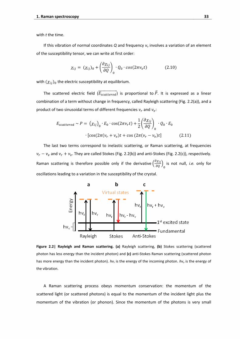
combination of a term without change in frequency, called Rayleigh scattering (Fig. 2.2(a)), and a
product of two sinusoidal terms of different frequencies and :
The last two terms correspond to inelastic scattering, or Raman scattering, at frequencies
and They are called Stokes (Fig. 2.2(b)) and anti-Stokes (Fig. 2.2(c)), respectively.
Raman scattering is therefore possible only if the derivative
is not null, i.e. only for
oscillations leading to a variation in the susceptibility of the crystal.
Figure 2.2| Rayleigh and Raman scattering. (a) Rayleigh scattering, (b) Stokes scattering (scattered
photon has less energy than the incident photon) and (c) anti-Stokes Raman scattering (scattered photon
has more energy than the incident photon). hνr is the energy of the incoming photon. hvv is the energy of
the vibration.
A Raman scattering process obeys momentum conservation: the momentum of the
scattered light (or scattered photons) is equal to the momentum of the incident light plus the
momentum of the vibration (or phonon). Since the momentum of the photons is very small

34 II. Methods
compared to dimensions of the unit-cell in the reciprocal space, only small wave-vectors (close
to the Brillouin-zone center) phonons are seen in first-order Raman scattering[83].
1.4. Selection rules
The symmetric second-rank Raman tensor for a given mode described by a normal
coordinate Q is defined as:
Assuming and to be the unit vectors of the polarization of the incident and analyzed
light, respectively, the Raman scattering intensity is proportional to:
Whether a Raman-active phonon can be observed under certain experimental conditions
regarding the incoming and scattered light is determined by equation 2.13. Using the Raman
selection rules, the symmetry of the Raman tensor and hence of the corresponding phonon can
be identified by Raman experiments with different scattering geometries[84].
The Porto notation is used to describe the configuration of the Raman experiment[84]. This
notation expresses the orientation of the crystal with respect to the polarization of the laser in
the excitation and analyzing directions. It consists of four letters:
a(bc)d (2.14)
where a is the direction of propagation of the incident light, b the direction of the
polarization of the incident light, c the direction of the polarization of the analyzer and d the
direction of propagation of the analyzed light.
In Fig. 2.3, we illustrate the two more common polarization measurement geometries in a
backscattering setup, where the incident and analyzed lights both propagate along the z-axis:
parallel configuration z(xx) and crossed configuration z(xy) .

1. Raman spectroscopy 35
Figure 2.3| Common polarization measurement geometries in Raman spectroscopy. Yellows arrows
denote the direction of propagation of the light in backscattering geometry. Black arrows are the
directions of the polarization of the incident light and the analyzer.
1.5. Experimental setup
The experiments were performed on a Renishaw inVia confocal Raman microscope[85]. As
shown in Fig. 2.4, it consists of: (1) several monochromatic light sources. We used lasers with
wavelengths of 442 nm, 532 nm and 633 nm; (2) waveplates to control the directions of
polarization of the incident and analyzed light; (3) a microscope to shine the light on the sample
and collect the scattered light; (4) a movable stage to move the sample in-situ and acquire maps;
(5) dielectric “edge” filters to cut the Rayleigh part of the spectra; (6) a diffraction grating for
dispersing the Raman scattered light; (7) a CCD camera for detecting this light.
Figure 2.4| Layout of Renishaw inVia confocal Raman microscope. The key components are highlighted.
Adapted from Renishaw’s documentation.

36 II. Methods
In this setup, the spectral resolution depends on the wavelength of the laser and the
diffraction grating. Here, it is ~1 cm-1/pixel. The spatial resolution is defined by the diffraction
limit and estimated from the spot-size at the surface of the sample. It is defined by the Rayleigh
criterion:
(2.15)
with d the diameter of the spot, λ the wavelength of the laser and NA the numerical
aperture of the objective[86]. Measurements were mostly performed with an exciting laser line of
532 nm, focused on the sample with an objective with a numerical aperture of 0.85, providing a
theoretical spot size of 760 nm.
In this thesis, the usual measurement consists of point-by-point mapping across a domain
wall in steps of 0.1 μm.
1.6. Principal Component Analysis
The maps generated contain thousands of spectra. In order to analyze these data, we use a
statistical approach based on principal component analysis (PCA).
PCA is used to express the data in such a way as to highlight their similarities and
differences. This can be used to identify specific spectral features otherwise hidden by the noise,
or automatically identify characteristic signatures in a Raman map. These features are called
principal components (PCs)[87]. Each spectrum S obtained from the mapping dataset, here a 3D
matrix corresponding to a map of Raman spectra, can be described as a linear combination of a
reduced number of PCs:
where Sa is the mean spectrum calculated as the normalized sum of all the spectra and tk is a
scalar, called the score. The number of PCs is equal to the number of spectra in the dataset.
These PCs are obtained from the singular value decomposition of the spectra in the mapping
dataset X. Let us assume that X is centered, i.e. column means have been subtracted and are
now equal to zero. X is expressed as the product of three matrices:
where the columns of U are the left-singular vectors of X, the diagonal entries of the diagonal
matrix D are the singular values of X and the column of V are the right-singular vectors of X (Vt is

1. Raman spectroscopy 37
the conjugate transpose matrix of V). In the vocabulary of the PCA, the columns of V are the PCs
and the projections of the data on the PCs are the scores tk given by:
The first PC is required to have the largest possible variance, in order to explain the larger
changes in the spectra. The second PC is computed under the constraint of being orthogonal to
the first PC and to have the largest possible variance. The other components are computed
likewise[87].
The next stage of the analysis consists then in determining the number of components
needed to reasonably describe the data: if too many PCs are retained, one might try to give a
physical meaning to something that is only noise; if too few PCs are retained, one might miss
important information. A key parameter to determine the number of PCs is the proportion of
total variance accounted for by each PC. This proportion P is:
(2.19)
where V(S) and V(PCk) are the variances of each spectrum and each PC, respectively. The lower is
P the less information is contained in the PC.
PCA is mainly used in chemometrics. It gives spatial and structural information about a
chemical system without any prior knowledge of the pure chemical products constituting it. As a
reference example, we show in Fig. 2.5 the result of PCA on a Raman map obtained from an area
of 62 x 62 pixels (pixels of 2 μm) on a contraceptive tablet[88]. It is known that the tablet contains
API, lactose monohydrate, maize starch and magnesium stearate. Fig. 2.5(a) shows the
comparison between the PCs and the pure spectra of the different chemical products. It is clear
that there is a direct one to one correspondence between both. For example, PC2 resembles the
API spectrum. Fig. 2.5(b) is a color map of the score of the different components. It is used to
identify the spatial repartition of the chemical products.

38 II. Methods
Figure 2.5| PCA in chemometrics. (a) First six PCs compared to pure spectra. (b) Score maps of the PCs of
a contraceptive tablet. Reproduced from [88].
PCA can also be used to map ferroelastic domains. Indeed, the rotation of the
crystallographic axes between different ferroelastic domains induces variations of the Raman
tensor and therefore the Raman intensity. PCA performed on a Raman mapping across several
domains captures these variations of intensity and gives the spatial distribution of the domains.
In the case of domain walls, and in particular 180°-domain walls, subtle changes in
comparison with a reference spectrum (extracted from a domain, far from the domain wall) and
localized on a small spatial area are studied. To a good approximation, every spectrum outside a
180°-domain wall is equal to the mean spectrum. All the deviations that happen at the domain
wall are then described by the second term of Eq. 2.16. In order to determine the physical
signification of these deviations, we classify them as peak shifts, FWHM changes and peak
intensity variations.
The interpretation of the results of the PCA on domain walls is beyond the classical scope of
the identification of different chemical species. The interpretation is therefore not
straightforward. However, a parallel can be done with the automatic correction of peak shifts

1. Raman spectroscopy 39
and peak width variations in Raman spectra[89,90] where the idea is to use PCA to identify small
peak variations due to instrumental perturbations and to automatically correct them[89,90].
In the case of domain walls, in order to understand the subtle changes and their signatures,
we perform simulations with Python 2.7. We consider a series of 300 spectra containing each a
single Lorentzian peak centered at 750 cm-1, with a FWHM of 20 cm-1. The discrete spectral
resolution is of 1 cm-1. The spectrum number is associated to a spatial position (in μm).
Twenty spectra are subjected to a distribution of peak shift between 0 and - 0.5 cm-1, as
shown in Fig. 2.6(a). PCA is applied to the series of simulated spectra: Fig. 2.6(d) shows the mean
spectrum and the only PC obtained. This PC resembles the first derivative of the Lorentzian peak.
Indeed, adding the derivative to the Lorentzian peak will increase the intensity on the left side of
the peak and decrease the intensity on the right side, shifting the Lorentzian to lower
frequencies.
In another series, the FWHM of twenty Lorentzians is decreased down to 2.5% before PCA is
applied, as shown in Fig. 2.6(b). Figure 2.6(e) shows the PC obtained: it is symmetric with an
increase of intensity at the center. Adding the PC to the Lorentzian peak will decrease the
intensity on its shoulders, reducing its FWHM.
We consider now a series of spectra containing two Lorentzian peaks with the same
intensity, centered at 400 cm-1 and 1200 cm-1. The intensity of the Lorentzian peak at higher
frequency is progressively decreased by 0.5%, decreasing the intensity ratio between the second
and the first Lorentzian, as shown in Fig. 2.6(c). Figure 2.6(f) shows the mean spectrum and the
PC obtained which resemble a Lorentzian peak with a negative intensity.

40 II. Methods
Figure 2.6| PCA on simulated spectra. Changes applied on 20 Lorentzian: (a) peak shift, (b) FWHM change
and (c) intensity variation. Lorentzian peak unmodified and PC obtained when performing PCA on (d) a
peak shift, (e) a FWHM change, (f) and an intensity variation. (g-i) are the corresponding scores for every
spectrum.
Figures 2.6(g-i) are the score of the PCs. They reveal the spatial position of the twenty
spectra affected by the changes. Qualitatively, the product between the PC and its score gives
the “direction” of the changes. As an example, the negative peak shift is characterized by an
increase of the intensity of the PC on the left side of the Lorentzian peak and a decrease on its
right side – because the PC score is positive.

2. Low-energy electron microscopy 41
2. Low-energy electron microscopy
2.1. Experimental setup
Low Energy Electron Microscopy (LEEM) is an electron in – electron out – technique. It is
based on the interaction between low energy incident electrons and the surface/near-surface
region of the sample. The use of low energy electrons limits the probing depth to a few
nanometers, optimizing the surface sensitivity, but also makes the technique extremely sensitive
to surface contamination. For both reasons, an ultra-high vacuum environment is required (base
pressure typically better than 1x10⁻⁹ mbar).
The experiments are performed using an Elmitec LEEM III, schematized in Fig. 2.7[91]. The
incident electron beam is emitted by (1) a thermionic LaB6 electron gun at an accelerating
voltage of U0 = -20 kV. The electrons are focused by (2) a set of magnetic condenser lenses. (3) A
magnetic beam separator deviates the electrons toward (4) the objective lens and the sample.
(5) The sample is at U0 + SV, where the Start Voltage (SV) defines the incident electron energy
with respect to the sample surface. The low-energy reflected and backscattered electrons travel
back through the objective lens, are reaccelerated to the gun voltage (because the objective lens
is grounded), and pass through the beam separator again. In the imaging column, (6) a set of
magneto-electric lenses are used to create a magnified image of the sample surface. (7) A
double multi-channel plate, screen and camera record the electron intensity as a function of SV
in a typical field of view of a few tens of microns. An angle limiting aperture in the back focal
plane of the objective lens cut off highly deviated electrons and improves spatial resolution.

42 II. Methods
Figure 2.7| Schematic of the electron optics of the Elmitec LEEM III.
The spatial resolution of a LEEM is better than 20 nm[92] (the ultimate resolution achieved is
4 nm[93]). It is limited by the spherical and chromatic aberrations of the objective lens. The
energy resolution is limited by the monochromaticity of the incident beam and typically below
0.5 eV for a LaB6 electron gun[91].
2.2. MEM-LEEM transition
At very low kinetic energy, the incident electrons have a kinetic energy below the surface
potential of the sample. They interact only weakly with the surface. This is called Mirror Electron
Microscopy (MEM). At higher kinetic energies (but < 10 V), electrons penetrate the first few
nanometers of the sample and are backscattered without any energy transfer to the sample.
This is Low Energy Electron Microscopy (LEEM).
The electron intensity on the screen versus the kinetic energy (or Start Voltage) of the
electrons is often referred as the reflectivity curve. At the transition between MEM and LEEM
regimes, the reflectivity drops because the energy of the electrons becomes sufficiently high to
overcome the surface potential barrier and penetrate the surface. The MEM-LEEM transition can
therefore be used to measure the surface potential of the regions of interest on the sample.
Figure 2.8(a-e) show five images acquired with the LEEM on a magnesium-doped lithium niobate
sample at different SV (see chapter IV for details). Clear bands with different intensities are
visible at different SV. They correspond to 180°-ferroelectric domains. Figure 2.8(f) plots the
electron intensity recorded in two domains of opposite polarization (labeled Pup and Pdown) as a

2. Low-energy electron microscopy 43
function of SV. The resulting curves can be fitted by a complementary error function (erfc) which
gives an accurate value of the inflection point:
with I0 the background intensity, A the amplitude, ς the width of the fitting function and Vt the
MEM-LEEM transition voltage. By convention, the inflection point is taken as the MEM-LEEM
transition point. The domain for which the electron intensity falls at lower start voltage has a
polarization pointing upward (Pup). The difference of energy (SV) between the two inflection
points gives the difference of surface potential between domains.
Figure 2.8| MEM-LEEM transition in magnesium-doped lithium niobate. MEM images at start voltages of
(a) 1.15 V and (b) 1.75 V. Same area observed in the region close to the MEM-LEEM transition at start
voltage of (c) 1.90 V and in LEEM at start voltages of (d) 2.10 V and (e) 2.70 V. (f) Electron intensity curves
extracted from Pup and Pdown domains.
An automated procedure is used to fit every pixels of the field of view and generate a map of
the surface potential values for the whole field of view.

44 II. Methods
2.3. Imaging physical topography
Any physical topography on a sample modifies the local electric fields and hence the
electrons trajectories. In MEM, electrons interact with a geometrical relief during the approach
to the surface and the acceleration away from it. As a result the electrons trajectories can be
strongly distorted and the contrast changes. These effects are theoretically described by Nepijko
et al.[94–96]. They studied the example of a protruding geometrical strip with height H. Fig. 2.9
shows the curves of the current density on the screen in relation to the initial current density in
the absence of object roughness. The calculation is performed for a LEEM setup without contrast
aperture and without converging lens between the sample and the image. The stripe appears as
a dark area. The steps look like a double line on the screen: wide weakly defined dark line and a
narrower bright one[95].
Figure 2.9| Contrast due to physical topography. Curves of the contrast distribution for protruding
geometric stripes of increasing height H (from (1) to (3)). Adapted from [95].
2.4. Imaging charged surfaces
In a ferroelectric material, the polar discontinuity at the bulk-terminated surface gives rise to
a net fixed surface charge. This surface charge density modulates the electrostatic potential
above the surface. In MEM, the incident electrons interact with the surface potential such that
positively charge regions sweep electrons inwards while negatively charge regions sweep
electrons outwards. Therefore, in MEM, without converging lens between the sample and the
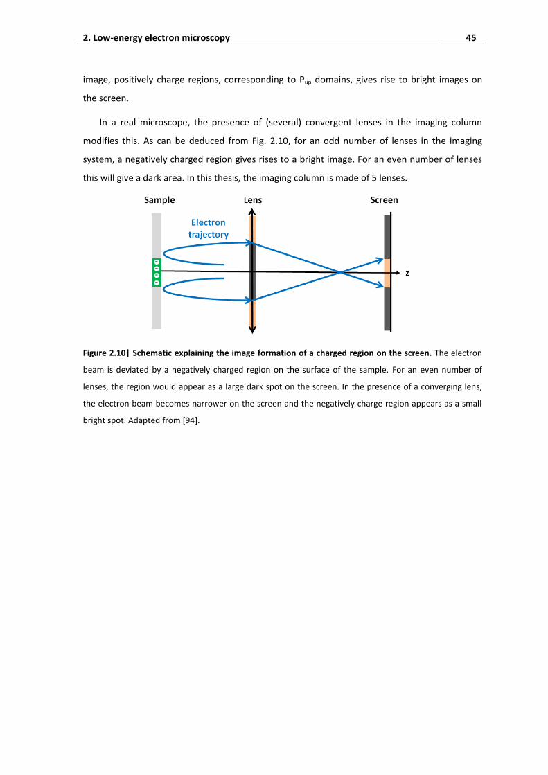
2. Low-energy electron microscopy 45
image, positively charge regions, corresponding to Pup domains, gives rise to bright images on
the screen.
In a real microscope, the presence of (several) convergent lenses in the imaging column
modifies this. As can be deduced from Fig. 2.10, for an odd number of lenses in the imaging
system, a negatively charged region gives rises to a bright image. For an even number of lenses
this will give a dark area. In this thesis, the imaging column is made of 5 lenses.
Figure 2.10| Schematic explaining the image formation of a charged region on the screen. The electron
beam is deviated by a negatively charged region on the surface of the sample. For an even number of
lenses, the region would appear as a large dark spot on the screen. In the presence of a converging lens,
the electron beam becomes narrower on the screen and the negatively charge region appears as a small
bright spot. Adapted from [94].

46 II. Methods
3. Other techniques
3.1. Dielectric spectroscopy
Dielectric spectroscopy measures the dielectric permittivity of a sample as a function of the
frequency of an applied electric field.
In a dielectric material, a small applied electric field induces a dielectric displacement
expressed by:
where ε0 is the dielectric permittivity of vacuum and ε* is the complex dielectric permittivity.
Because and are vectors, ε* is a tensor. In particular, for a periodic electric field oscillating at
a frequency f, - , ε* can be written:
where ε’( ) and ε’’( ) are the real and imaginary part of the complex dielectric permittivity,
respectively.
The simplest analysis of the frequency response of a dielectric material is known as the
Debye model. It describes the response of an ideal, non-interacting population of dipoles to the
external periodic electric field. The dipoles follow the oscillations of the electric field up to a
certain frequency. Above this frequency, the field reversal and the dipole reorientation become
out-of-phase and dissipate energy[97].
In this model, the change of dielectric displacement is proportional to its actual value[98]:
where τD is a characteristic relaxation time. Within this hypothesis, the complex dielectric
function is written:
where ε∞
is the permittivity at the high frequency limit and εs is the low frequency static
permittivity. This relaxation process is characterized by a peak in the imaginary part ε’’ and a
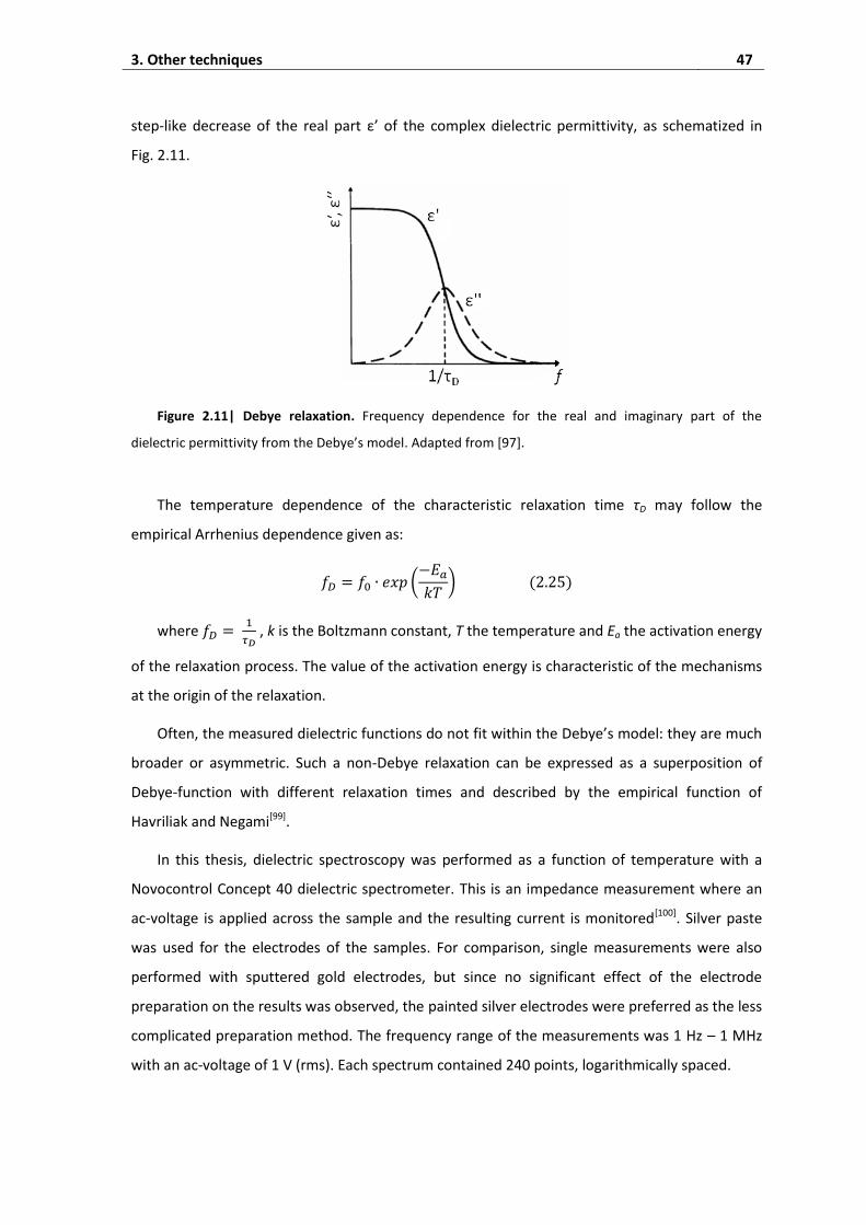
3. Other techniques 47
step-like decrease of the real part ε’ of the complex dielectric permittivity, as schematized in
Fig. 2.11.
Figure 2.11| Debye relaxation. Frequency dependence for the real and imaginary part of the
dielectric permittivity from the Debye’s model. Adapted from [97].
The temperature dependence of the characteristic relaxation time τD may follow the
empirical Arrhenius dependence given as:
where
, k is the Boltzmann constant, T the temperature and Ea the activation energy
of the relaxation process. The value of the activation energy is characteristic of the mechanisms
at the origin of the relaxation.
Often, the measured dielectric functions do not fit within the Debye’s model: they are much
broader or asymmetric. Such a non-Debye relaxation can be expressed as a superposition of
Debye-function with different relaxation times and described by the empirical function of
Havriliak and Negami[99].
In this thesis, dielectric spectroscopy was performed as a function of temperature with a
Novocontrol Concept 40 dielectric spectrometer. This is an impedance measurement where an
ac-voltage is applied across the sample and the resulting current is monitored[100]. Silver paste
was used for the electrodes of the samples. For comparison, single measurements were also
performed with sputtered gold electrodes, but since no significant effect of the electrode
preparation on the results was observed, the painted silver electrodes were preferred as the less
complicated preparation method. The frequency range of the measurements was 1 Hz – 1 MHz
with an ac-voltage of 1 V (rms). Each spectrum contained 240 points, logarithmically spaced.
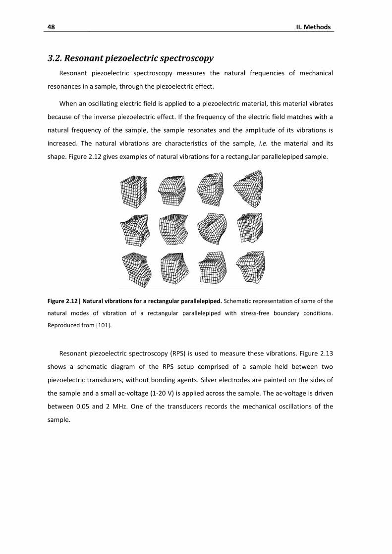
48 II. Methods
3.2. Resonant piezoelectric spectroscopy
Resonant piezoelectric spectroscopy measures the natural frequencies of mechanical
resonances in a sample, through the piezoelectric effect.
When an oscillating electric field is applied to a piezoelectric material, this material vibrates
because of the inverse piezoelectric effect. If the frequency of the electric field matches with a
natural frequency of the sample, the sample resonates and the amplitude of its vibrations is
increased. The natural vibrations are characteristics of the sample, i.e. the material and its
shape. Figure 2.12 gives examples of natural vibrations for a rectangular parallelepiped sample.
Figure 2.12| Natural vibrations for a rectangular parallelepiped. Schematic representation of some of the
natural modes of vibration of a rectangular parallelepiped with stress-free boundary conditions.
Reproduced from [101].
Resonant piezoelectric spectroscopy (RPS) is used to measure these vibrations. Figure 2.13
shows a schematic diagram of the RPS setup comprised of a sample held between two
piezoelectric transducers, without bonding agents. Silver electrodes are painted on the sides of
the sample and a small ac-voltage (1-20 V) is applied across the sample. The ac-voltage is driven
between 0.05 and 2 MHz. One of the transducers records the mechanical oscillations of the
sample.
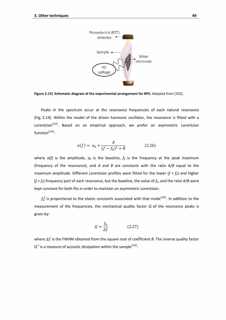
3. Other techniques 49
Figure 2.13| Schematic diagram of the experimental arrangement for RPS. Adapted from [102].
Peaks in the spectrum occur at the resonance frequencies of each natural resonance
(Fig. 2.14). Within the model of the driven harmonic oscillator, the resonance is fitted with a
Lorentzian[103]. Based on an empirical approach, we prefer an asymmetric Lorentzian
function[104]:
where a(f) is the amplitude, a0 is the baseline, f0 is the frequency at the peak maximum
(frequency of the resonance), and A and B are constants with the ratio A/B equal to the
maximum amplitude. Different Lorentzian profiles were fitted for the lower (f < f0) and higher
(f > f0) frequency part of each resonance, but the baseline, the value of f0, and the ratio A/B were
kept constant for both fits in order to maintain an asymmetric Lorentzian.
is proportional to the elastic constants associated with that mode[103]. In addition to the
measurement of the frequencies, the mechanical quality factor Q of the resonance peaks is
given by:
where is the FWHM obtained from the square root of coefficient B. The inverse quality factor
Q-1 is a measure of acoustic dissipation within the sample[103].
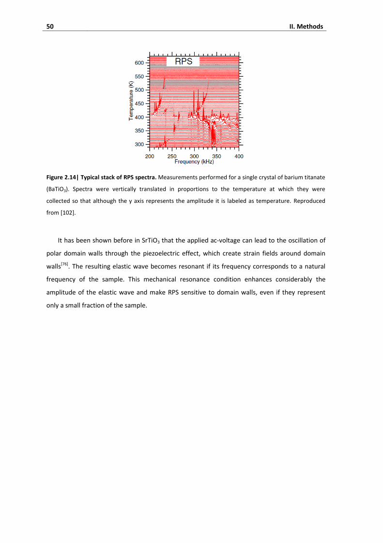
50 II. Methods
Figure 2.14| Typical stack of RPS spectra. Measurements performed for a single crystal of barium titanate
(BaTiO3). Spectra were vertically translated in proportions to the temperature at which they were
collected so that although the y axis represents the amplitude it is labeled as temperature. Reproduced
from [102].
It has been shown before in SrTiO3 that the applied ac-voltage can lead to the oscillation of
polar domain walls through the piezoelectric effect, which create strain fields around domain
walls[76]. The resulting elastic wave becomes resonant if its frequency corresponds to a natural
frequency of the sample. This mechanical resonance condition enhances considerably the
amplitude of the elastic wave and make RPS sensitive to domain walls, even if they represent
only a small fraction of the sample.
51
III. Interaction between defects and domain walls in lithium niobate
180°-domain walls in magnesium-doped lithium niobate (Mg:LiNbO3) are conductive under
above-band gap illumination. It has been proposed that the conduction is possible because of (i)
the inclination of the domain walls with respect to the polar axis that create local head-to-head
polarizations and (ii) the creation of free carriers by UV light[13]. However, others mechanisms
can also be involved. For example, conduction at domain walls reported in other ferroelectrics,
such as bismuth ferrite or lead zirconate titanate, is thought to be due to the presence of
defects, such as oxygen vacancies, at and near domain walls[10–12].
Conductivity could also be an effect of the local strain observed at domain walls[105,106]. This
explanation is based on an analogy with experiments on perovskites under high pressure where
it has been shown that a hydrostatic pressure, thus strong deformations, can induce a transition
from insulator to metal. Indeed, the first effect of pressure is to reduce the inter-atomic
distances, leading to strong modifications of the electronic band overlap and thus the electronic
band structure. This insulator-metal transition has been reported in bismuth ferrite at
~55 GPa[107] and in lead vanadate at ~2.5 GPa[108]. Similarly, the strain at domain walls could
locally increase the conductivity. Also, illumination with UV light may increase the strain via the
photostrictive effect[109] and allow conduction at domain walls.
This chapter is structured as follows: in the first part, the general properties of lithium
niobate are reviewed with a focus on defects and their influence on the polarization. Then, we
present dielectric spectroscopy measurements performed on single crystals of lithium niobate
with different densities of domain walls. The goal is to probe the interaction between defects
and domain walls. In the last part, we show the Raman signature observed at domain walls in
magnesium-doped lithium niobate and its evolution with poling, annealing and above-band gap
illumination. This gives insights into the structure of defects at domain walls for different
concentration of magnesium and allows us to investigate the influence of UV illumination on the
structural properties of domain walls.
The observations are then discussed in relation to the possible mechanisms at the origin of
domain wall conductivity in lithium niobate.
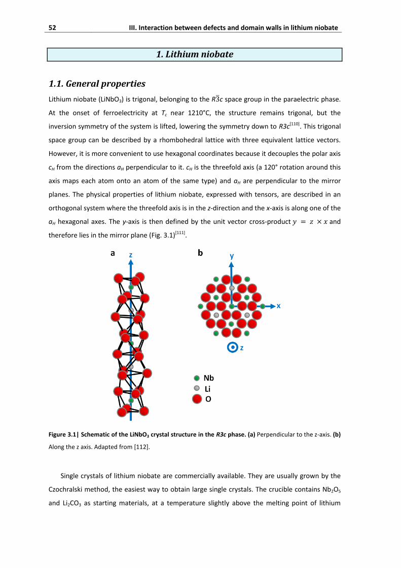
52 III. Interaction between defects and domain walls in lithium niobate
1. Lithium niobate
1.1. General properties
Lithium niobate (LiNbO3) is trigonal, belonging to the R c space group in the paraelectric phase.
At the onset of ferroelectricity at Tc near 1210°C, the structure remains trigonal, but the
inversion symmetry of the system is lifted, lowering the symmetry down to R3c[110]. This trigonal
space group can be described by a rhombohedral lattice with three equivalent lattice vectors.
However, it is more convenient to use hexagonal coordinates because it decouples the polar axis
cH from the directions aH perpendicular to it. cH is the threefold axis (a 120° rotation around this
axis maps each atom onto an atom of the same type) and aH are perpendicular to the mirror
planes. The physical properties of lithium niobate, expressed with tensors, are described in an
orthogonal system where the threefold axis is in the z-direction and the x-axis is along one of the
aH hexagonal axes. The y-axis is then defined by the unit vector cross-product and
therefore lies in the mirror plane (Fig. 3.1)[111].
Figure 3.1| Schematic of the LiNbO3 crystal structure in the R3c phase. (a) Perpendicular to the z-axis. (b)
Along the z axis. Adapted from [112].
Single crystals of lithium niobate are commercially available. They are usually grown by the
Czochralski method, the easiest way to obtain large single crystals. The crucible contains Nb2O5
and Li2CO3 as starting materials, at a temperature slightly above the melting point of lithium
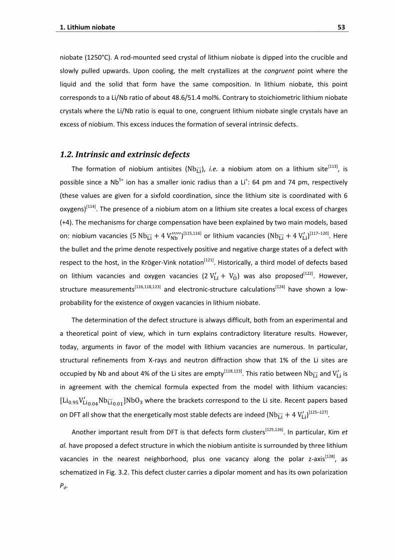
1. Lithium niobate 53
niobate (1250°C). A rod-mounted seed crystal of lithium niobate is dipped into the crucible and
slowly pulled upwards. Upon cooling, the melt crystallizes at the congruent point where the
liquid and the solid that form have the same composition. In lithium niobate, this point
corresponds to a Li/Nb ratio of about 48.6/51.4 mol%. Contrary to stoichiometric lithium niobate
crystals where the Li/Nb ratio is equal to one, congruent lithium niobate single crystals have an
excess of niobium. This excess induces the formation of several intrinsic defects.
1.2. Intrinsic and extrinsic defects
The formation of niobium antisites ( ), i.e. a niobium atom on a lithium site[113], is
possible since a Nb5+ ion has a smaller ionic radius than a Li+: 64 pm and 74 pm, respectively
(these values are given for a sixfold coordination, since the lithium site is coordinated with 6
oxygens)[114]. The presence of a niobium atom on a lithium site creates a local excess of charges
(+4). The mechanisms for charge compensation have been explained by two main models, based
on: niobium vacancies (
)[115,116] or lithium vacancies (
)[117–120]. Here
the bullet and the prime denote respectively positive and negative charge states of a defect with
respect to the host, in the Kröger-Vink notation[121]. Historically, a third model of defects based
on lithium vacancies and oxygen vacancies (2
) was also proposed[122]. However,
structure measurements[116,118,123] and electronic-structure calculations[124] have shown a low-
probability for the existence of oxygen vacancies in lithium niobate.
The determination of the defect structure is always difficult, both from an experimental and
a theoretical point of view, which in turn explains contradictory literature results. However,
today, arguments in favor of the model with lithium vacancies are numerous. In particular,
structural refinements from X-rays and neutron diffraction show that 1% of the Li sites are
occupied by Nb and about 4% of the Li sites are empty[118,123]. This ratio between and
is
in agreement with the chemical formula expected from the model with lithium vacancies:
where the brackets correspond to the Li site. Recent papers based
on DFT all show that the energetically most stable defects are indeed (
)[125–127].
Another important result from DFT is that defects form clusters[125,126]. In particular, Kim et
al. have proposed a defect structure in which the niobium antisite is surrounded by three lithium
vacancies in the nearest neighborhood, plus one vacancy along the polar z-axis[128], as
schematized in Fig. 3.2. This defect cluster carries a dipolar moment and has its own polarization
Pd.

54 III. Interaction between defects and domain walls in lithium niobate
Figure 3.2| Schematic of a polar defect structure involving one and four
. Pup denotes the
spontaneous polarization. Pd denotes the defect polarization. The red triangles indicate the position of
oxygen planes. Adapted from [128].
The incorporation of external defects (or dopants) competes with the internal defects
already present in the congruent crystal. For doping with magnesium, the mechanism of
incorporation has been investigated by nuclear magnetic resonance, Raman spectroscopy and
optical absorption measurements[129–134]. It proceeds in two steps. For low doping levels, Mg2+
ions are localized on Li sites, decreasing the number of . Above a threshold value, in the
range 4.5-5.3 mol%, Mg2+ ions occupy both Li and NbNb positions.
1.3. Polaronic states
The defects structures mentioned above involve strong chemical modifications. However,
electronic modifications such as polarons are also observed in lithium niobate[135].
When an electron is placed in an ionic crystal, the Coulomb interaction between the electron
and the surrounding positive ions results in a strong coupling that can trap the electron[136]. The
electron repels the negative ions and attracts the positive ions, as schematically shown in
Fig. 3.3. These movements create a potential-well for the electron. They also induce a local
polarization. The electron and the associated local polarization are called a polaron.
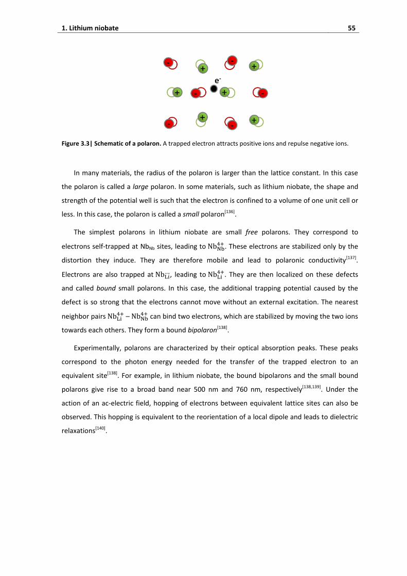
1. Lithium niobate 55
Figure 3.3| Schematic of a polaron. A trapped electron attracts positive ions and repulse negative ions.
In many materials, the radius of the polaron is larger than the lattice constant. In this case
the polaron is called a large polaron. In some materials, such as lithium niobate, the shape and
strength of the potential well is such that the electron is confined to a volume of one unit cell or
less. In this case, the polaron is called a small polaron[136].
The simplest polarons in lithium niobate are small free polarons. They correspond to
electrons self-trapped at NbNb sites, leading to . These electrons are stabilized only by the
distortion they induce. They are therefore mobile and lead to polaronic conductivity[137].
Electrons are also trapped at , leading to
. They are then localized on these defects
and called bound small polarons. In this case, the additional trapping potential caused by the
defect is so strong that the electrons cannot move without an external excitation. The nearest
neighbor pairs –
can bind two electrons, which are stabilized by moving the two ions
towards each others. They form a bound bipolaron[138].
Experimentally, polarons are characterized by their optical absorption peaks. These peaks
correspond to the photon energy needed for the transfer of the trapped electron to an
equivalent site[138]. For example, in lithium niobate, the bound bipolarons and the small bound
polarons give rise to a broad band near 500 nm and 760 nm, respectively[138,139]. Under the
action of an ac-electric field, hopping of electrons between equivalent lattice sites can also be
observed. This hopping is equivalent to the reorientation of a local dipole and leads to dielectric
relaxations[140].

56 III. Interaction between defects and domain walls in lithium niobate
1.4. Domain structure
The ferroelectric domains of lithium niobate are characterized by (a) a small displacement of
the Nb atoms to an asymmetric position along the z-axis within the same oxygen octahedron (b)
a corresponding motion of Li atoms from one octahedron to the adjacent vacant octahedron
(Fig. 3.4). Since the direction of the polarization is defined by the motion of these ions, only two
opposite orientations are possible for domains[112]. We label “Pup” a domain that has a
polarization pointing upward at the surface and “Pdown” a domain that has a polarization in the
opposite direction. They are separated by non-ferroelastic 180°-domain walls.
Figure 3.4| Ferroelectric domains in lithium niobate. Cation motion during domain reversal leading to
unit cells with polarization Pup and Pdown. Adapted from [128].
Domains structures can be created at room temperature by applying an electric field above
the coercive field (~21 kV/mm for congruent lithium niobate[55]). However, during this process,
the polarization of the defect structures does not flip. Polar defect structures maintain their own
polarization Pd, leading to the existence of a macroscopic internal electric field. The value of this
field has been estimated from the asymmetry of the hysteresis loop to be of the order of
3 kV/mm[55]. Upon annealing at > 150°C, the internal electric field vanishes, meaning that the
polar defect structures align with the main polarization direction[112].
An optical image of a sample with a regular pattern of ferroelectric domains is shown in
Fig. 3.5: they fully cross the sample in the y-direction and are 9.3 μm wide. They are optically
visible because the supplier performed a chemical etching with HF that induces a difference of
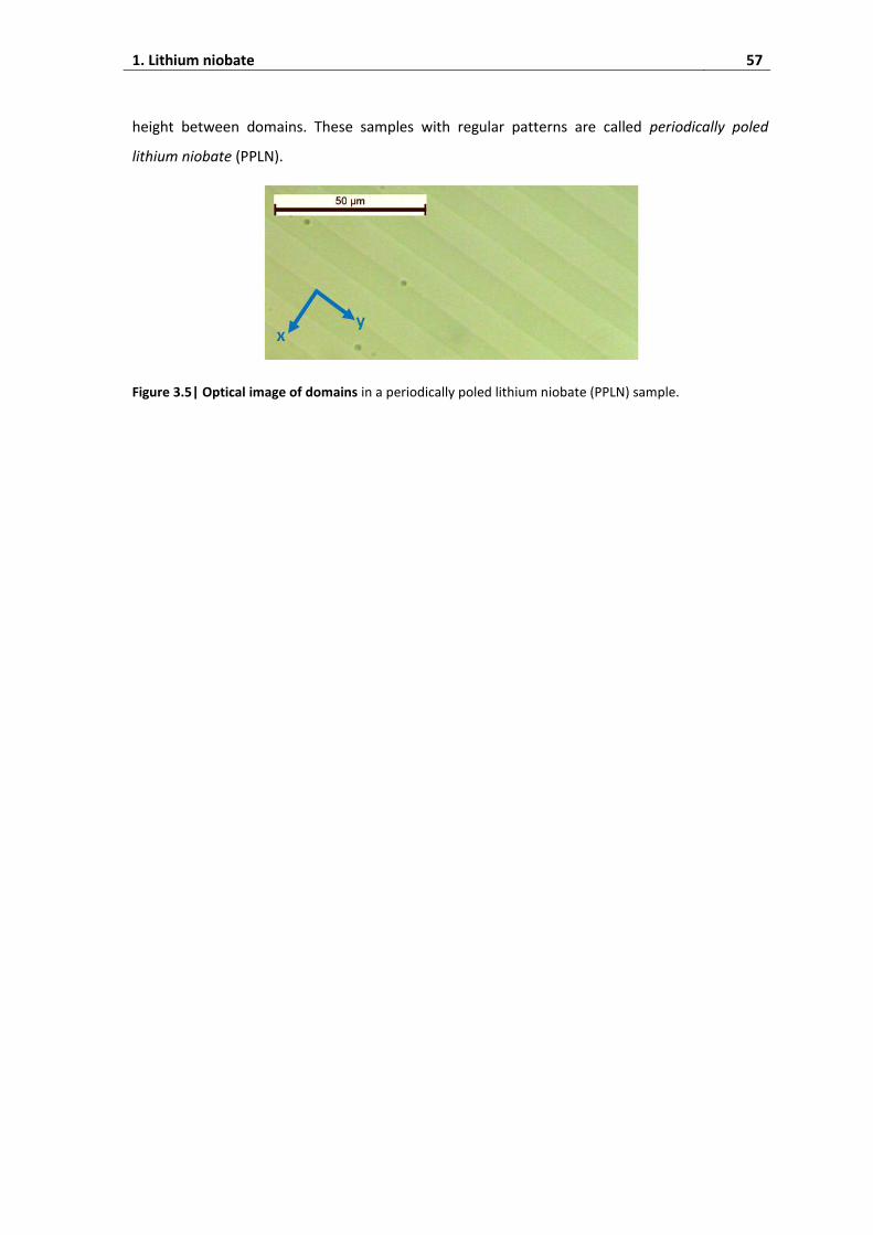
1. Lithium niobate 57
height between domains. These samples with regular patterns are called periodically poled
lithium niobate (PPLN).
Figure 3.5| Optical image of domains in a periodically poled lithium niobate (PPLN) sample.
58 III. Interaction between defects and domain walls in lithium niobate
2. Stabilization of electronic defects at domain walls as seen by
dielectric spectroscopy
We present dielectric spectroscopy measurements performed on congruent lithium niobate
single crystals with different densities of domain walls. The goal is to probe the interaction
between defects and domain walls.
2.1. State of the art
In a dielectric spectroscopy measurement, the permittivity strongly increases if the ac-
electric field applied on the dielectric material is strong enough to induce irreversible
movements of domain walls. This extrinsic contribution of domain wall mobility has been
investigated in lead zirconate titanate (Pb(Zr,Ti)O3) by measuring the temperature dependence
of the dielectric constant with an applied ac-electric field: at low temperature, domain walls are
frozen and the permittivity is low; at higher temperature, domain walls move and the
permittivity increases, with a clear deviation from the Curie-Weiss law[141,142]. Many other
experiments performed on lead zirconate titanate[141,143,144] confirm that dielectric spectroscopy
is a powerful tool to study ferroelectric domain walls.
Dielectric properties of congruent lithium niobate have been studied on thin films[145],
polycrystalline[146–148], and single crystals samples[149,150]. In single crystals, investigations by
Mansingh and Dhar[150] show the absence of dispersion of the real part of the permittivity below
125°C while Chen et al.[149] observe a relaxation above 150°C. Since this relaxation is well
described by the Debye model, they attribute it to the response of dipoles in the sample.
The dielectric spectrum of iron and magnesium doped samples is characterized by new
dielectric relaxations[151,152]. In iron-doped lithium niobate, the relaxation arises from clusters of
Fe2+/Fe3+ that slowly relax as a unity with the ac-voltage. After a heating treatment around
600°C, iron clusters are destroyed and iron ions are homogeneously distributed over the crystal,
leading to the disappearance of the relaxation[151]. In magnesium-doped lithium niobate, it is
proposed that the electrons from the donor centers are usually trapped in (
)
defects complexes. High-temperature poling breaks these defect complexes. The transition of
the liberated electrons between the and the NbNb gives rise to the dielectric relaxation.
Heating around 200°C activates the motion of (already mobiles at 100°C[153]), re-forming the
defect complexes and causing the relaxation to vanish[152].

2. Stabilization of electronic defects at domain walls as seen by dielectric spectroscopy
59
This short overview of the state of the art illustrates that dielectric spectroscopy can be used
to study ferroelectric domain walls and defects. We therefore investigated congruent lithium
niobate samples with intrinsic defects and different densities of domain walls.
2.2. Experimental conditions
Six samples of congruent single crystals have been studied. A periodically poled single
crystal, commercially available from HC Photonics Corps, labeled as PPLNa, has a domain period
of 20.4 μm (i.e. a domain wall density of 98 mm-1). A periodically poled single crystal with a
domain period of 28 μm (i.e. a domain wall density of 71 mm-1), labeled as PPLNb, and a
monodomain sample single crystal labeled as MLN1, were purchased from EQ Photonics GmbH.
Samples MLN2a, MLN2b and MLN2c were purchased from PI-KEM Ltd and cut from a single
domain wafer. All samples had platelet geometry with ~5 x 5 x 0.5 mm3 dimensions and short
edges along the z direction. The monodomain wafers were poled by the manufacturer near the
Curie temperature, without field-cooling. The characteristics of the samples are summarized in
table 3.1.
Name Domain period (μm) Supplier
PPLNa 20.4 HC Photonics
PPLNb 28 EQ Photonics
MLN1 Monodomain EQ Photonics
MLN2a Monodomain PI-KEM
MLN2b Monodomain PI-KEM
MLN2c Monodomain PI-KEM Table 3.1| Main characteristics of the samples.
Dielectric spectroscopy was performed as a function of temperature to study the evolution
of the dielectric permittivity and loss. These measurements were made between 273 K and
473 K in 25 K steps. They were repeated after a high-temperature annealing (up to 860 K)
between 143 K and 573 K in 15 K steps on heating and cooling. The frequency range of the
measurement was 1 Hz – 1 MHz with an ac-voltage of 1 V (rms).
2.3. Monodomain samples
Monodomain samples are taken as references to understand the dielectric response of a
single crystal without domain walls. In order to get a reliable comparison of monodomain and
periodically poled samples, we defined the following criteria: (i) one monodomain sample
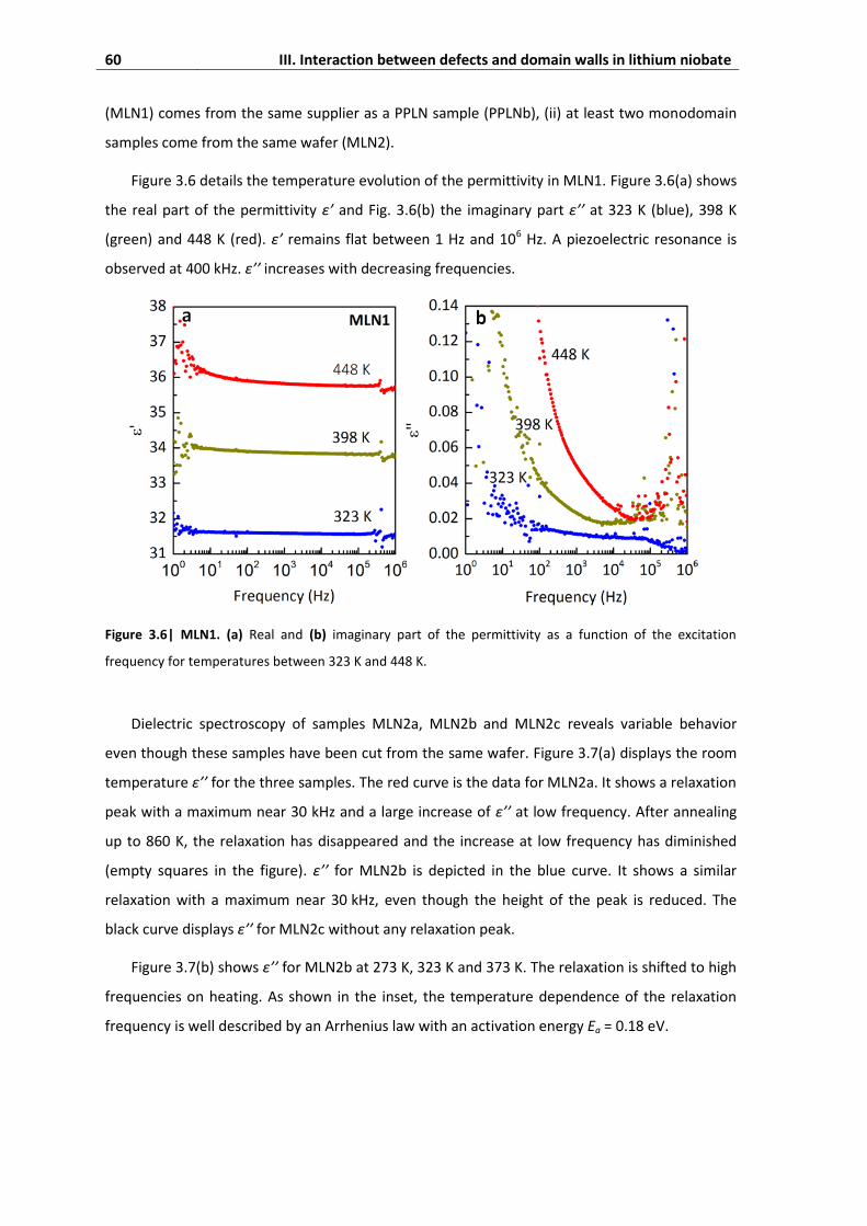
60 III. Interaction between defects and domain walls in lithium niobate
(MLN1) comes from the same supplier as a PPLN sample (PPLNb), (ii) at least two monodomain
samples come from the same wafer (MLN2).
Figure 3.6 details the temperature evolution of the permittivity in MLN1. Figure 3.6(a) shows
the real part of the permittivity ε’ and Fig. 3.6(b) the imaginary part ε’’ at 323 K (blue), 398 K
(green) and 448 K (red). ε’ remains flat between 1 Hz and 106 Hz. A piezoelectric resonance is
observed at 400 kHz. ε’’ increases with decreasing frequencies.
Figure 3.6| MLN1. (a) Real and (b) imaginary part of the permittivity as a function of the excitation
frequency for temperatures between 323 K and 448 K.
Dielectric spectroscopy of samples MLN2a, MLN2b and MLN2c reveals variable behavior
even though these samples have been cut from the same wafer. Figure 3.7(a) displays the room
temperature ε’’ for the three samples. The red curve is the data for MLN2a. It shows a relaxation
peak with a maximum near 30 kHz and a large increase of ε’’ at low frequency. After annealing
up to 860 K, the relaxation has disappeared and the increase at low frequency has diminished
(empty squares in the figure). ε’’ for MLN2b is depicted in the blue curve. It shows a similar
relaxation with a maximum near 30 kHz, even though the height of the peak is reduced. The
black curve displays ε’’ for MLN2c without any relaxation peak.
Figure 3.7(b) shows ε’’ for MLN2b at 273 K, 323 K and 373 K. The relaxation is shifted to high
frequencies on heating. As shown in the inset, the temperature dependence of the relaxation
frequency is well described by an Arrhenius law with an activation energy Ea = 0.18 eV.
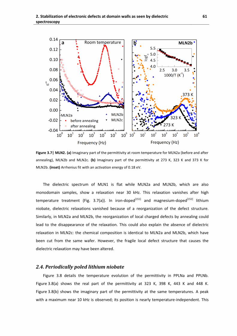
2. Stabilization of electronic defects at domain walls as seen by dielectric spectroscopy
61
Figure 3.7| MLN2. (a) Imaginary part of the permittivity at room temperature for MLN2a (before and after
annealing), MLN2b and MLN2c. (b) Imaginary part of the permittivity at 273 K, 323 K and 373 K for
MLN2b. (inset) Arrhenius fit with an activation energy of 0.18 eV.
The dielectric spectrum of MLN1 is flat while MLN2a and MLN2b, which are also
monodomain samples, show a relaxation near 30 kHz. This relaxation vanishes after high
temperature treatment (Fig. 3.7(a)). In iron-doped[151] and magnesium-doped[152] lithium
niobate, dielectric relaxations vanished because of a reorganization of the defect structure.
Similarly, in MLN2a and MLN2b, the reorganization of local charged defects by annealing could
lead to the disappearance of the relaxation. This could also explain the absence of dielectric
relaxation in MLN2c: the chemical composition is identical to MLN2a and MLN2b, which have
been cut from the same wafer. However, the fragile local defect structure that causes the
dielectric relaxation may have been altered.
2.4. Periodically poled lithium niobate
Figure 3.8 details the temperature evolution of the permittivity in PPLNa and PPLNb.
Figure 3.8(a) shows the real part of the permittivity at 323 K, 398 K, 443 K and 448 K.
Figure 3.8(b) shows the imaginary part of the permittivity at the same temperatures. A peak
with a maximum near 10 kHz is observed; its position is nearly temperature-independent. This
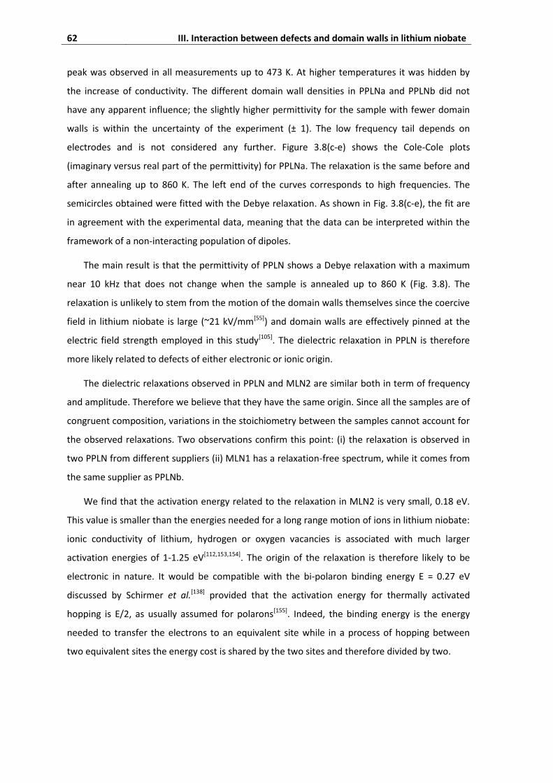
62 III. Interaction between defects and domain walls in lithium niobate
peak was observed in all measurements up to 473 K. At higher temperatures it was hidden by
the increase of conductivity. The different domain wall densities in PPLNa and PPLNb did not
have any apparent influence; the slightly higher permittivity for the sample with fewer domain
walls is within the uncertainty of the experiment (± 1). The low frequency tail depends on
electrodes and is not considered any further. Figure 3.8(c-e) shows the Cole-Cole plots
(imaginary versus real part of the permittivity) for PPLNa. The relaxation is the same before and
after annealing up to 860 K. The left end of the curves corresponds to high frequencies. The
semicircles obtained were fitted with the Debye relaxation. As shown in Fig. 3.8(c-e), the fit are
in agreement with the experimental data, meaning that the data can be interpreted within the
framework of a non-interacting population of dipoles.
The main result is that the permittivity of PPLN shows a Debye relaxation with a maximum
near 10 kHz that does not change when the sample is annealed up to 860 K (Fig. 3.8). The
relaxation is unlikely to stem from the motion of the domain walls themselves since the coercive
field in lithium niobate is large (~21 kV/mm[55]) and domain walls are effectively pinned at the
electric field strength employed in this study[105]. The dielectric relaxation in PPLN is therefore
more likely related to defects of either electronic or ionic origin.
The dielectric relaxations observed in PPLN and MLN2 are similar both in term of frequency
and amplitude. Therefore we believe that they have the same origin. Since all the samples are of
congruent composition, variations in the stoichiometry between the samples cannot account for
the observed relaxations. Two observations confirm this point: (i) the relaxation is observed in
two PPLN from different suppliers (ii) MLN1 has a relaxation-free spectrum, while it comes from
the same supplier as PPLNb.
We find that the activation energy related to the relaxation in MLN2 is very small, 0.18 eV.
This value is smaller than the energies needed for a long range motion of ions in lithium niobate:
ionic conductivity of lithium, hydrogen or oxygen vacancies is associated with much larger
activation energies of 1-1.25 eV[112,153,154]. The origin of the relaxation is therefore likely to be
electronic in nature. It would be compatible with the bi-polaron binding energy E = 0.27 eV
discussed by Schirmer et al.[138] provided that the activation energy for thermally activated
hopping is E/2, as usually assumed for polarons[155]. Indeed, the binding energy is the energy
needed to transfer the electrons to an equivalent site while in a process of hopping between
two equivalent sites the energy cost is shared by the two sites and therefore divided by two.
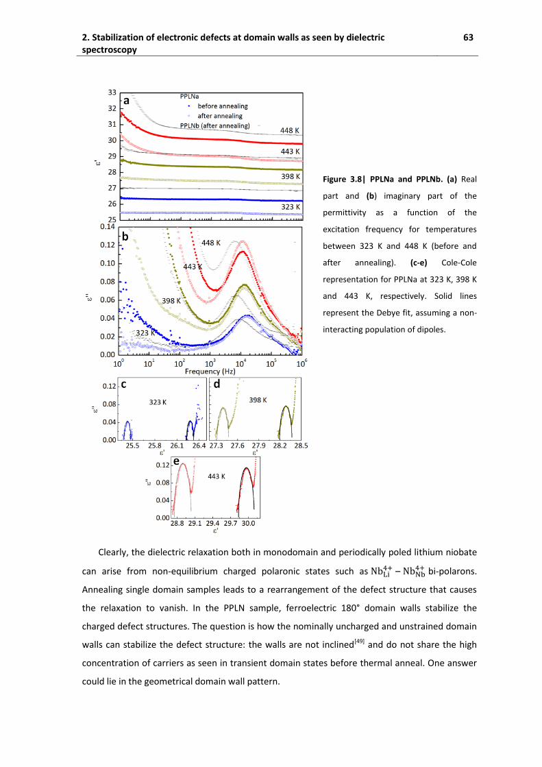
2. Stabilization of electronic defects at domain walls as seen by dielectric spectroscopy
63
Figure 3.8| PPLNa and PPLNb. (a) Real
part and (b) imaginary part of the
permittivity as a function of the
excitation frequency for temperatures
between 323 K and 448 K (before and
after annealing). (c-e) Cole-Cole
representation for PPLNa at 323 K, 398 K
and 443 K, respectively. Solid lines
represent the Debye fit, assuming a non-
interacting population of dipoles.
Clearly, the dielectric relaxation both in monodomain and periodically poled lithium niobate
can arise from non-equilibrium charged polaronic states such as –
bi-polarons.
Annealing single domain samples leads to a rearrangement of the defect structure that causes
the relaxation to vanish. In the PPLN sample, ferroelectric 180° domain walls stabilize the
charged defect structures. The question is how the nominally uncharged and unstrained domain
walls can stabilize the defect structure: the walls are not inclined[49] and do not share the high
concentration of carriers as seen in transient domain states before thermal anneal. One answer
could lie in the geometrical domain wall pattern.
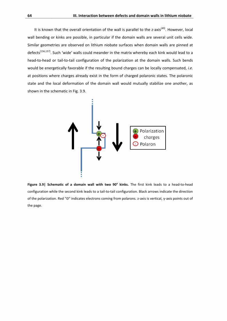
64 III. Interaction between defects and domain walls in lithium niobate
It is known that the overall orientation of the wall is parallel to the z-axis[49]. However, local
wall bending or kinks are possible, in particular if the domain walls are several unit cells wide.
Similar geometries are observed on lithium niobate surfaces when domain walls are pinned at
defects[156,157]. Such ‘wide’ walls could meander in the matrix whereby each kink would lead to a
head-to-head or tail-to-tail configuration of the polarization at the domain walls. Such bends
would be energetically favorable if the resulting bound charges can be locally compensated, i.e.
at positions where charges already exist in the form of charged polaronic states. The polaronic
state and the local deformation of the domain wall would mutually stabilize one another, as
shown in the schematic in Fig. 3.9.
Figure 3.9| Schematic of a domain wall with two 90° kinks. The first kink leads to a head-to-head
configuration while the second kink leads to a tail-to-tail configuration. Black arrows indicate the direction
of the polarization. Red “ʘ“ indicates electrons coming from polarons. z-axis is vertical, y-axis points out of
the page.
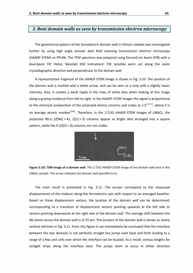
3. Bent domain walls as seen by transmission electron microscopy 65
3. Bent domain walls as seen by transmission electron microscopy
The geometrical pattern of the ferroelectric domain wall in lithium niobate was investigated
further by using high angle annular dark field scanning transmission electron microscopy
(HAADF-STEM) on PPLNb. The TEM specimen was prepared using focused ion beam (FIB) with a
dual-beam FEI Helios Nanolab 650 instrument. FIB lamellas were cut along the polar
crystallographic direction and perpendicular to the domain wall.
A representative fragment of the HAADF-STEM image is shown in Fig. 3.10. The position of
the domain wall is marked with a white arrow, and can be seen as a strip with a slightly lower
intensity. Also, it creates a weak ripple in the rows of white dots when looking at this image
along a grazing incidence from left to right. In the HAADF-STEM images the signal is proportional
to the chemical composition of the projected atomic columns and scales as I~Z1.6-1.9, where Z is
an average atomic number[158]. Therefore, in the [1 00] HAADF-STEM images of LiNbO3, the
projected Nb-Li (Z[Nb] = 41, Z[Li] = 3) columns appear as bright dots arranged into a square
pattern, while the O (Z[O] = 8) columns are not visible.
Figure 3.10| TEM image of a domain wall. The [1 00] HAADF-STEM image of the domain wall area in the
LiNbO3 sample. The arrow indicates the domain wall (parallel to it).
The main result is presented in Fig. 3.11. The arrows correspond to the measured
displacements of the niobium along the ferroelectric axis with respect to an averaged baseline.
Based on these displacement vectors, the location of the domain wall can be determined,
corresponding to a transition of displacement vectors pointing upwards at the left side to
vectors pointing downwards at the right side of the domain wall. The average shift between the
Nb atoms across the domain wall is of 25 pm. The location of the domain wall is shown as nearly
vertical red lines in Fig. 3.11. From this figure it can immediately be concluded that the interface
between the two domains is not perfectly straight but jumps exist back and forth leading to a
range of a few unit cells over which the interface can be located. As a result, various lengths for
straight strips along the interface exist. The jumps seem to occur in either direction
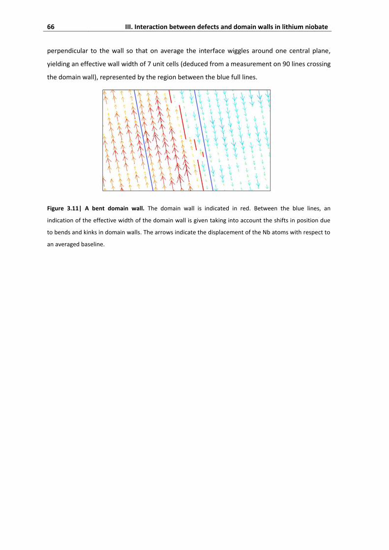
66 III. Interaction between defects and domain walls in lithium niobate
perpendicular to the wall so that on average the interface wiggles around one central plane,
yielding an effective wall width of 7 unit cells (deduced from a measurement on 90 lines crossing
the domain wall), represented by the region between the blue full lines.
Figure 3.11| A bent domain wall. The domain wall is indicated in red. Between the blue lines, an
indication of the effective width of the domain wall is given taking into account the shifts in position due
to bends and kinks in domain walls. The arrows indicate the displacement of the Nb atoms with respect to
an averaged baseline.
4. Stabilization of polar defect structures at domain walls as seen by Raman spectroscopy
67
4. Stabilization of polar defect structures at domain walls as seen by
Raman spectroscopy
Dielectric spectroscopy is a macroscopic, bulk measurement. To get a microscopic picture of
the interaction between defects and domain walls, Raman spectroscopy is a powerful tool. We
present the Raman signature observed at domain walls in magnesium-doped lithium niobate
and its evolution with poling and annealing. This allows us to study the interaction between
polar defects and domain walls for different concentration of magnesium dopants. We also
investigate the influence of UV illumination on the structural properties of domain walls in
5 mol% magnesium-doped lithium niobate, known to present photo-conductive domain walls[13].
4.1. State of the art
The number of articles reporting Raman spectroscopy investigations on 180° domain walls in
lithium niobate is large[52,159–167]. Indeed, lithium niobate is a perfect system to study domain
walls with Raman micro-spectroscopy: 1) from symmetry there is no contrast between domains
of opposite polarization and therefore any change observed in the vicinity of domain walls can
be attributed to the domain walls without ambiguity; 2) the Raman spectrum is well defined and
does not require long acquisition times. These studies were performed in backscattering
geometry with the incident light along the ferroelectric z-axis. They reveal intensity and
frequency variations of the Raman modes in the vicinity of domain walls.
Figure 3.12 shows a typical Raman spectrum in z(xx) configuration where 13 modes are
recognized according the work of Margueron et al.[168]. The three most studied modes in the
literature on domain walls are indicated.
Intensity changes in defect free samples. Stone et al. reported changes in the Raman
spectra at domain walls in near-stoichiometric lithium niobate[159]. They observed an increase of
intensity in spectral regions that correspond to phonons that propagate at an angle with respect
to the incident light. But, in principle, Raman spectroscopy only probes phonons which
propagate in the same direction as the incident light. This is the case in the bulk of lithium
niobate. They argue that the intensity variations are an indication that domain walls absorb
phonon momentum.
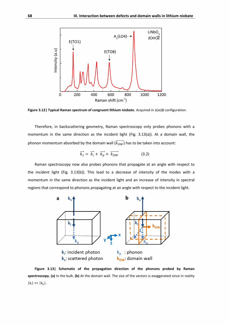
68 III. Interaction between defects and domain walls in lithium niobate
Figure 3.12| Typical Raman spectrum of congruent lithium niobate. Acquired in z(xx) configuration.
Therefore, in backscattering geometry, Raman spectroscopy only probes phonons with a
momentum in the same direction as the incident light (Fig. 3.13(a)). At a domain wall, the
phonon momentum absorbed by the domain wall ( ) has to be taken into account:
(3.2)
Raman spectroscopy now also probes phonons that propagate at an angle with respect to
the incident light (Fig. 3.13(b)). This lead to a decrease of intensity of the modes with a
momentum in the same direction as the incident light and an increase of intensity in spectral
regions that correspond to phonons propagating at an angle with respect to the incident light.
Figure 3.13| Schematic of the propagation direction of the phonons probed by Raman
spectroscopy. (a) In the bulk. (b) At the domain wall. The size of the vectors is exaggerated since in reality
|ki| << |kp|.

4. Stabilization of polar defect structures at domain walls as seen by Raman spectroscopy
69
Intensity changes in congruent samples. Zelenovskiy and al. studied a congruent PPLN
sample[52]. At domain walls, intensity maxima were observed for transversal E modes (E(TO1)
and E(TO8)), whereas intensity minima were observed for longitudinal mode A1(LO4). These
results were confirmed by Fontana et al.[162,163]. They were interpreted as an effect of the
strain/electric field arising at the domain wall. Indeed, the Raman intensity is proportional to the
square of the derivative of the polarizability with respect to the normal vibration coordinates,
which is influenced by mechanical stress and/or electric field acting on the lattice. Capek et al.
also reported changes of intensity of A1(LO4) mode but they interpreted it as a pyroelectric
effect[164]. They suggested that the Raman laser causes uneven charging across domain walls due
to the pyroelectric effect, leading to birefringence in the xy plane via the electro-optic effect.
This birefringence is supposed to modify the polarization of the incident and analyzed light,
inducing small changes of intensity of the modes with respect to the domains[164].
Frequency changes in congruent samples. To identify and isolate the Raman changes due to
defects, Stone et al. compared the results obtained for congruent lithium niobate with those
obtained for near-stoichiometric lithium niobate[165]. They observed larger frequency shifts in the
congruent sample than in the near-stoichiometric lithium niobate. Capek et al. confirmed these
observations[164]. Zelenovskiy et al. observed frequency shifts of E(TO1) and E(TO8) modes at
domain walls, while the other modes did not shift[166]. Contradictory results were presented by
Kong et al. who observed an increase of A1(LO4) frequency as large as 1.5 cm-1[167]. All these
shifts were interpreted as an effect of defects localized at domain walls.
This short state of the art shows that the physical interpretation of subtle changes observed
in the Raman spectra near domain walls is complex. Many explanations are plausible and require
supplementary information given by the influence of external parameters. Therefore we
investigated domain walls in samples for different levels of magnesium doping, before and after
annealing, with and without UV illumination.
4.2. Experimental conditions
We investigated a congruent periodically poled lithium niobate from EQ Photonics GmbH.
The others crystals under study were commercially available congruent lithium niobate doped
with different amount of magnesium: 0 mol% Mg-doped from CrysTec GmbH; 1 mol%, 2 mol%
and 3 mol% from Crystal Technology, 5 mol% from Yamaju Ceramics and 7 mol% from Union
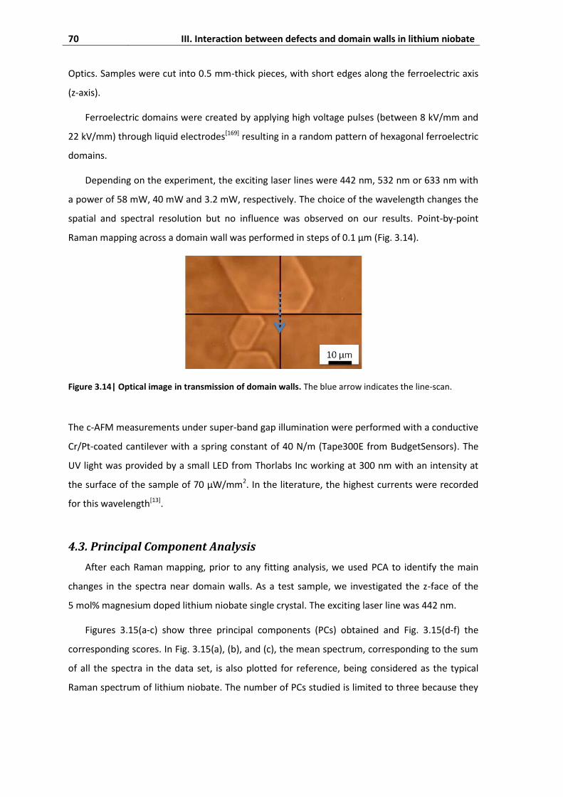
70 III. Interaction between defects and domain walls in lithium niobate
Optics. Samples were cut into 0.5 mm-thick pieces, with short edges along the ferroelectric axis
(z-axis).
Ferroelectric domains were created by applying high voltage pulses (between 8 kV/mm and
22 kV/mm) through liquid electrodes[169] resulting in a random pattern of hexagonal ferroelectric
domains.
Depending on the experiment, the exciting laser lines were 442 nm, 532 nm or 633 nm with
a power of 58 mW, 40 mW and 3.2 mW, respectively. The choice of the wavelength changes the
spatial and spectral resolution but no influence was observed on our results. Point-by-point
Raman mapping across a domain wall was performed in steps of 0.1 μm (Fig. 3.14).
Figure 3.14| Optical image in transmission of domain walls. The blue arrow indicates the line-scan.
The c-AFM measurements under super-band gap illumination were performed with a conductive
Cr/Pt-coated cantilever with a spring constant of 40 N/m (Tape300E from BudgetSensors). The
UV light was provided by a small LED from Thorlabs Inc working at 300 nm with an intensity at
the surface of the sample of 70 μW/mm2. In the literature, the highest currents were recorded
for this wavelength[13].
4.3. Principal Component Analysis
After each Raman mapping, prior to any fitting analysis, we used PCA to identify the main
changes in the spectra near domain walls. As a test sample, we investigated the z-face of the
5 mol% magnesium doped lithium niobate single crystal. The exciting laser line was 442 nm.
Figures 3.15(a-c) show three principal components (PCs) obtained and Fig. 3.15(d-f) the
corresponding scores. In Fig. 3.15(a), (b), and (c), the mean spectrum, corresponding to the sum
of all the spectra in the data set, is also plotted for reference, being considered as the typical
Raman spectrum of lithium niobate. The number of PCs studied is limited to three because they

4. Stabilization of polar defect structures at domain walls as seen by Raman spectroscopy
71
account for 84.2% (66.5% + 13.5% + 4.2%) of the total variance, as shown in Fig. 3.16. The fourth
component, which account for only 0.04% more, and all the others contain basically only noise.
In Fig. 3.15(a), PC1 resembles the mean Raman spectrum. By direct comparison with the
results of the simulation in chapter II (section 1.6), this PC describes changes of intensity of the
global spectrum. These variations of intensity are usually referred as “noise” in Raman
experiments: they are due to fluctuations of the laser intensity and drift of the sample holder
during the measurement. This is why the score of this PC is not correlated with the domain
structure (Fig. 3.15(d)).
Figures 3.15(b,c) present many features centered at the same frequencies as the different
Raman modes: they are similar to what was observed in the simulation of peak shifts or peak
intensity variations in chapter II. In Fig. 3.15(b), the main features of the second PC are indicated
by blue arrows. At 154 cm-1, the PC resembles the first derivative of a Lorentzian and by
comparison with simulations, is interpreted as a shift of the E(TO1) mode centered at 154 cm-1.
By comparison with simulations, the large change of intensity of the PC near 615 cm-1 is a
growing peak. The third PC is dominated by two features indicated by blue arrows: a shift of
E(TO1) at 154 cm-1 and a shift of A1(LO4) at 870 cm-1. Figures 3.15(d-f) show the score of the first,
second and third PCs, respectively. The score of the second PC presents a high contrast in the
position of the domain wall as determined by optical microscopy. The score of the third PC
reveals a small contrast between both domains. This contrast is not expected for 180°-domains.
It is in fact due to the internal field of lithium niobate and will be explained in details in
section 4.6.

72 III. Interaction between defects and domain walls in lithium niobate
Figure 3.15| Result of the PCA analysis. Mean spectrum and (a) first PC, (b) second PC, (c) third PC. (d-f)
are the corresponding scores for every spectrum.
Figure 3.16| Percent of total variance accounted by the PCs.

4. Stabilization of polar defect structures at domain walls as seen by Raman spectroscopy
73
The interpretation of the PCA is that (i) E(TO1) peak position is different in domains and
shifts at the domain wall (ii) A1(LO4) peak position is different in domains. PCA has then been
performed on selected frequency ranges to study individually these two modes: between 40 and
200 cm-1 for E(TO1), between 750 and 1000 cm-1 for A1(LO4). The first two PCs obtained are
shown in Fig. 3.17(a) for E(TO1) and (b) for A1(LO4). They are similar to the features observed in
Fig. 3.15. For both modes, PC1 resembles the Raman mode and PC2 its derivative. PCA tells us
that the sum of the two PCs describes well the modes. Thus, both modes can be seen as the sum
of the mean spectrum and its derivative. In particular, this means that for these two modes
spectra are expandable in a Taylor series:
(3.3)
where b1 and b2 are the Taylor coefficients, L is the constant lineshape function and
is the
derivative of the spectrum with respect to the frequency f. Within the hypothesis of Lorentzian
(or Voigt) lineshape:
and (3.4)
where A is the peak maximum of the spectrum and Δf is the peak shift. Thus, once a
reference spectrum is chosen and its first derivative calculated, the Taylor coefficients can be
estimated by multiple linear regressions of the reference spectrum and its derivative on the
complete series of spectra. Then, the calculated regression coefficients are used to determine
the peak shift Δf.
Figure 3.17| Result of the PCA analysis on individual modes. (a) E(TO1), (b) A1(LO4).
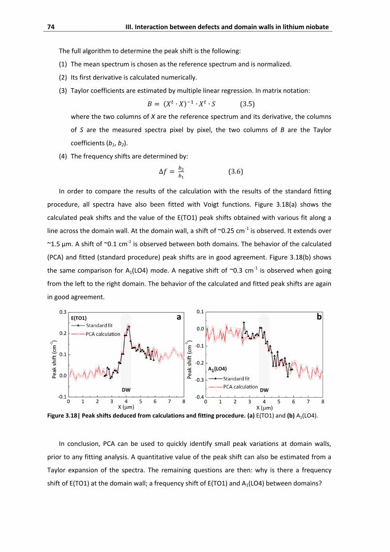
74 III. Interaction between defects and domain walls in lithium niobate
The full algorithm to determine the peak shift is the following:
(1) The mean spectrum is chosen as the reference spectrum and is normalized.
(2) Its first derivative is calculated numerically.
(3) Taylor coefficients are estimated by multiple linear regression. In matrix notation:
(3.5)
where the two columns of X are the reference spectrum and its derivative, the columns
of S are the measured spectra pixel by pixel, the two columns of B are the Taylor
coefficients (b1, b2).
(4) The frequency shifts are determined by:
(3.6)
In order to compare the results of the calculation with the results of the standard fitting
procedure, all spectra have also been fitted with Voigt functions. Figure 3.18(a) shows the
calculated peak shifts and the value of the E(TO1) peak shifts obtained with various fit along a
line across the domain wall. At the domain wall, a shift of ~0.25 cm-1 is observed. It extends over
~1.5 μm. A shift of ~0.1 cm-1 is observed between both domains. The behavior of the calculated
(PCA) and fitted (standard procedure) peak shifts are in good agreement. Figure 3.18(b) shows
the same comparison for A1(LO4) mode. A negative shift of ~0.3 cm-1 is observed when going
from the left to the right domain. The behavior of the calculated and fitted peak shifts are again
in good agreement.
Figure 3.18| Peak shifts deduced from calculations and fitting procedure. (a) E(TO1) and (b) A1(LO4).
In conclusion, PCA can be used to quickly identify small peak variations at domain walls,
prior to any fitting analysis. A quantitative value of the peak shift can also be estimated from a
Taylor expansion of the spectra. The remaining questions are then: why is there a frequency
shift of E(TO1) at the domain wall; a frequency shift of E(TO1) and A1(LO4) between domains?

4. Stabilization of polar defect structures at domain walls as seen by Raman spectroscopy
75
4.4. Absence of signature of momentum absorption by domain walls
Before studying in detail the influence of magnesium dopants on the Raman signature, let us
first investigate the idea of Stone et al. who argued that domain walls absorb phonon
momentum[159]. We performed Raman measurements on the z-face and y-face of the congruent
periodically poled lithium niobate sample with the exciting laser lines at 532 nm and 633 nm.
Lithium niobate is a polar uniaxial crystal. Due to the anisotropy of the crystal, the phonons
in which atoms are displaced parallel to the ferroelectric axis z have a different frequency from
that of phonons in which atoms are displaced perpendicular to the ferroelectric axis, i.e in the xy
plane[83]. In particular, the frequency of the excited phonons depends on the angle θ between z
and the direction of propagation of the incident light (Fig. 3.19(a))[170]. However, the phonons
frequency is invariant in the xy plane, i.e the y-face (Fig. 3.19(b)).
Therefore, if phonon momentum is absorbed perpendicularly to the domain wall plane, the
frequency of the phonons will be shifted in Raman measurements performed on the z-face, but
not on the y-face. Fig. 3.19 sketches the geometry of the measurements at domain walls, with
two phonons: the first one propagates along the ferroelectric axis and has a frequency f1, the
second one propagates at an angle θ and has a frequency f2. For measurements on the y-face,
f1 = f2.
Figure 3.19| Geometry of the measurements at domain walls. (a) On the z-face. (b) On the y-face. f1 and
f2 denote the frequency of the phonons.
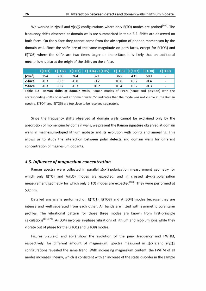
76 III. Interaction between defects and domain walls in lithium niobate
We worked in z(yx) and y(zx) configurations where only E(TO) modes are probed[168]. The
frequency shifts observed at domain walls are summarized in table 3.2. Shifts are observed on
both faces. On the y-face they cannot come from the absorption of phonon momentum by the
domain wall. Since the shifts are of the same magnitude on both faces, except for E(TO3) and
E(TO6) where the shifts are two times larger on the z-face, it is likely that an additional
mechanism is also at the origin of the shifts on the z-face.
E(TO1) E(TO2) E(TO3) E(TO4) - E(TO5) E(TO6) E(TO7) E(TO8) E(TO9)
(cm-1) 154 236 264 321 365 431 580 -
Z-face -0.3 -0.3 -0.8 -0.2 +0.8 +0.2 -0.4 -
Y-face -0.3 -0.2 -0.3 +0.2 +0.4 +0.2 -0.3 - Table 3.2| Raman shifts at domain walls. Raman modes of PPLN (name and position) with the
corresponding shifts observed at domain walls. “-” indicates that the mode was not visible in the Raman
spectra. E(TO4) and E(TO5) are too close to be resolved separately.
Since the frequency shifts observed at domain walls cannot be explained only by the
absorption of momentum by domain walls, we present the Raman signature observed at domain
walls in magnesium-doped lithium niobate and its evolution with poling and annealing. This
allows us to study the interaction between polar defects and domain walls for different
concentration of magnesium dopants.
4.5. Influence of magnesium concentration
Raman spectra were collected in parallel z(xx) polarization measurement geometry for
which only E(TO) and A1(LO) modes are expected, and in crossed z(yx) polarization
measurement geometry for which only E(TO) modes are expected[168]. They were performed at
532 nm.
Detailed analysis is performed on E(TO1), E(TO8) and A1(LO4) modes because they are
intense and well separated from each other. All bands are fitted with symmetric Lorentzian
profiles. The vibrational pattern for those three modes are known from first-principle
calculations[171,172]: A1(LO4) involves in-phase vibrations of lithium and niobium ions while they
vibrate out of phase for the E(TO1) and E(TO8) modes.
Figures 3.20(a-c) and (d-f) show the evolution of the peak frequency and FWHM,
respectively, for different amount of magnesium. Spectra measured in z(xx) and z(yx)
configurations revealed the same trend. With increasing magnesium content, the FWHM of all
modes increases linearly, which is consistent with an increase of the static disorder in the sample
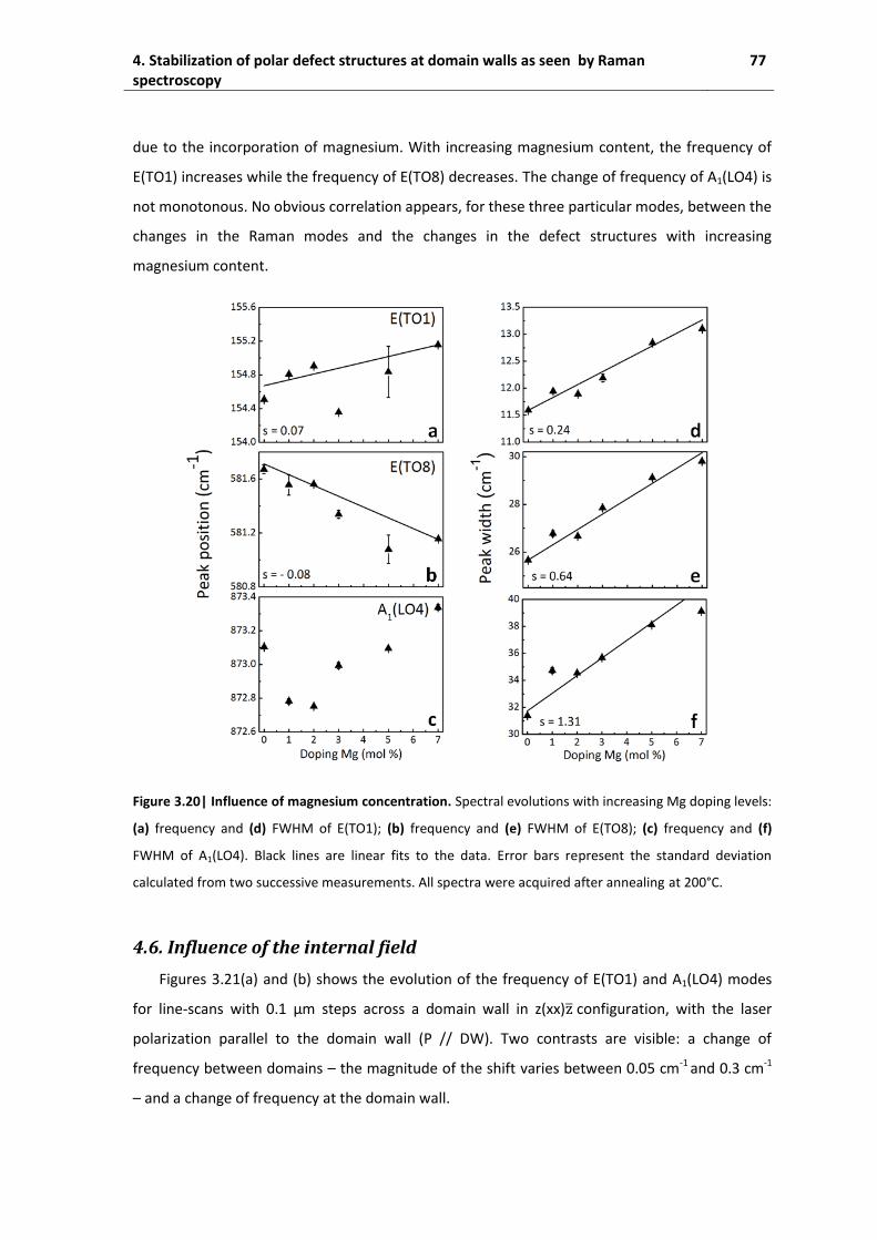
4. Stabilization of polar defect structures at domain walls as seen by Raman spectroscopy
77
due to the incorporation of magnesium. With increasing magnesium content, the frequency of
E(TO1) increases while the frequency of E(TO8) decreases. The change of frequency of A1(LO4) is
not monotonous. No obvious correlation appears, for these three particular modes, between the
changes in the Raman modes and the changes in the defect structures with increasing
magnesium content.
Figure 3.20| Influence of magnesium concentration. Spectral evolutions with increasing Mg doping levels:
(a) frequency and (d) FWHM of E(TO1); (b) frequency and (e) FWHM of E(TO8); (c) frequency and (f)
FWHM of A1(LO4). Black lines are linear fits to the data. Error bars represent the standard deviation
calculated from two successive measurements. All spectra were acquired after annealing at 200°C.
4.6. Influence of the internal field
Figures 3.21(a) and (b) shows the evolution of the frequency of E(TO1) and A1(LO4) modes
for line-scans with 0.1 μm steps across a domain wall in z(xx) configuration, with the laser
polarization parallel to the domain wall (P // DW). Two contrasts are visible: a change of
frequency between domains – the magnitude of the shift varies between 0.05 cm-1 and 0.3 cm-1
– and a change of frequency at the domain wall.

78 III. Interaction between defects and domain walls in lithium niobate
We first consider the contrast between virgin and reversed domains. In the undoped sample,
the frequency of E(TO1), E(TO8) and A1(LO4) is lower in reversed domains (R) – the Pdown surface
– consistent with previous observations[173,174]. The frequency shifts have been explained by the
presence of polar defects and the internal field they create; this is notably based on the
observations that (i) frequency shifts are larger for the congruent composition than for the
stoichiometric composition[173], and that (ii) the frequency shift and the amplitude of the internal
field exhibit the same time dependence upon domain reversal[174].
Figure 3.21| Influence of the internal field. Peak position of (a) E(TO1) and (b) A1(LO4) for line-scan from
reversed (R) to virgin (V) domains for different amounts of magnesium before annealing. The data are
vertically shifted for clarity and the scale bar gives the amplitude of the frequency shift.
As shown in Fig. 3.21, the frequency shifts of the Raman peaks do not change monotonically
with Mg doping. In 1%, 2% and 3% Mg-doped lithium niobate the frequency of all modes is
slightly higher in reversed domains. On the other hand, in 5% and 7% Mg-doped lithium niobate,
the frequency of E(TO1) and E(TO8) is decreased while the frequency of A1(LO4) is increased in
reversed domains. It is known from measurements of the transient current during switching that
Mg-doped lithium niobate presents an internal field[175]. By analogy with undoped lithium
niobate, the frequency shifts between domains in Mg-doped lithium niobate are attributed to
this internal field. The non-monotonic behavior of the internal field can be understood by a
change in the structure of polar defects: the studies of incorporation of Mg2+ ions into lithium
niobate have shown that Mg ions first replace NbLi for MgO concentrations lower than 4.5-
5.3 mol%, and then replace Li and Nb ions on their own sites[115,129–134]. Therefore, the Raman
contrast that we observe for samples doped with more than 5 mol% of magnesium results from
the internal field due to (1) the disappearance of all , (2) the appearance of
.
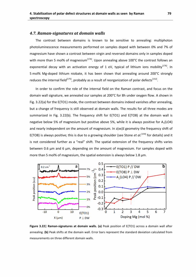
4. Stabilization of polar defect structures at domain walls as seen by Raman spectroscopy
79
4.7. Raman-signatures at domain walls
The contrast between domains is known to be sensitive to annealing: multiphoton
photoluminescence measurements performed on samples doped with between 0% and 7% of
magnesium have shown a contrast between virgin and reversed domains only in samples doped
with more than 5 mol% of magnesium[176]. Upon annealing above 100°C the contrast follows an
exponential decay with an activation energy of 1 eV, typical of lithium ions mobility[176]. In
5 mol% Mg-doped lithium niobate, it has been shown that annealing around 200°C strongly
reduces the internal field[175], probably as a result of reorganization of polar defects[152].
In order to confirm the role of the internal field on the Raman contrast, and focus on the
domain wall signature, we annealed our samples at 200°C for 8h under oxygen flow. A shown in
Fig. 3.22(a) for the E(TO1) mode, the contrast between domains indeed vanishes after annealing,
but a change of frequency is still observed at domain walls. The results for all three modes are
summarized in Fig. 3.22(b). The frequency shift for E(TO1) and E(TO8) at the domain wall is
negative below 5% of magnesium but positive above 5%, while it is always positive for A1(LO4)
and nearly independent on the amount of magnesium. In z(xx) geometry the frequency shift of
E(TO8) is always positive; this is due to a growing shoulder (see Stone et al.[159] for details) and it
is not considered further as a “real” shift. The spatial extension of the frequency shifts varies
between 0.6 μm and 6 μm, depending on the amount of magnesium. For samples doped with
more than 5 mol% of magnesium, the spatial extension is always below 1.8 μm.
Figure 3.22| Raman-signatures at domain walls. (a) Peak position of E(TO1) across a domain wall after
annealing. (b) Peak shifts at the domain wall. Error bars represent the standard deviation calculated from
measurements on three different domain walls.
80 III. Interaction between defects and domain walls in lithium niobate
4.8. Discussion
Frequency shifts of Raman modes at domain walls in lithium niobate have already been
reported and interpreted (i) as an effect of the strong electric and associated strain field
accompanying smooth polarization reversal at the domain wall[164,166,167] or (ii) as a change in the
defect cluster concentration and configurations at the domain wall[159,165]. Specifically, for
undoped lithium niobate, our observation of decreasing frequency of E(TO1) and E(TO8) at the
domain wall while increasing frequency of A1(LO4) is consistent with previous measurements,
which were interpreted as an effect of defect clusters, involving [165].
Here, the systematic study of the evolution of the Raman modes for the whole series of Mg
concentrations and before and after annealing sheds more light on the origin of the frequency
shifts. First, it is clear that the smooth polarization reversal at the domain wall and the resulting
electric field alone cannot account for all the observations since it would not explain the doping-
dependence of the frequency shifts of the E modes. A reduction of the depolarization field at
domain walls due to a better bulk screening could not explain the change of sign of peak shifts.
Conversely, a simple picture where the dopants would segregate at the walls would not be
consistent with the observations, notably because the FWHM of E(TO8) and A1(LO4) does not
change at the domain wall, whereas they vary strongly in the bulk with variations of Mg content.
We therefore propose that both polarization reversal and defects have to be taken into account.
The correlation between the frequency shifts for the E modes and the change in defect
structure for high Mg-doping points to the role of defects, and changes in defect structure. For
samples doped with 5 mol% of magnesium and more, the new behavior observed at domain
walls is a consequence of the change of configuration of polar defects described earlier.
However, detailed examination shows that the frequency pattern at the domain wall differs
from the signature of polar defects observed in the bulk, notably as seen by comparing Fig. 3.21
and 3.22. This can be understood in two ways: (1) the frequency shifts observed involve a
combination of effects resulting from the defect structure and the electric (strain) field in the
vicinity of the wall or (2) new defect structure have been stabilized at domain walls. Since
previous measurements based on defect-luminescence microscopy have shown that the defect
structure remains similar at the domain wall[177,178], the second hypothesis is less plausible. In
both cases, the contrast at domain walls still exists after annealing while it is no longer present in
the domains, meaning that defects have been stabilized at the domain walls but annealed out of
the bulk.
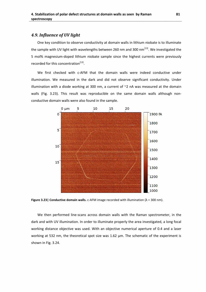
4. Stabilization of polar defect structures at domain walls as seen by Raman spectroscopy
81
4.9. Influence of UV light
One key condition to observe conductivity at domain walls in lithium niobate is to illuminate
the sample with UV light with wavelengths between 260 nm and 300 nm[13]. We investigated the
5 mol% magnesium-doped lithium niobate sample since the highest currents were previously
recorded for this concentration[13].
We first checked with c-AFM that the domain walls were indeed conductive under
illumination. We measured in the dark and did not observe significant conductivity. Under
illumination with a diode working at 300 nm, a current of ~2 nA was measured at the domain
walls (Fig. 3.23). This result was reproducible on the same domain walls although non-
conductive domain walls were also found in the sample.
Figure 3.23| Conductive domain walls. c-AFM image recorded with illumination (λ = 300 nm).
We then performed line-scans across domain walls with the Raman spectrometer, in the
dark and with UV illumination. In order to illuminate properly the area investigated, a long focal
working distance objective was used. With an objective numerical aperture of 0.4 and a laser
working at 532 nm, the theoretical spot size was 1.62 μm. The schematic of the experiment is
shown in Fig. 3.24.

82 III. Interaction between defects and domain walls in lithium niobate
Figure 3.24| Experimental setup for the Raman spectroscopy investigations under UV light. The green
line symbolizes the laser. The black arrows indicate the direction of the polarization in the domains.
Figure 3.25 shows the peak positions of E(TO1) and E(TO8) observed at domain walls, in the
dark and with illumination. The two curves match perfectly and the same frequency shift is
observed at the domain wall. The same observation is made on all the frequency shifts observed
at domain walls.
Figure 3.25| Peak shifts under illumination. Peak position of (a) E(TO1) and (b) E(TO8) across a domain
wall with/without illumination at 300 nm.
A straightforward conclusion is that the UV light does not influence the Raman signatures at
domain walls while it induces a small current localized at domain walls. However, the conditions
of illumination in the AFM and the Raman spectrometer are slightly different. In particular, the
distance between the area investigated and the diode is larger in the Raman experiment due to
the presence of the microscope objective lens. Experiments where c-AFM and Raman
spectroscopy are performed on the same setup are in progress to guarantee that the domain
wall investigated is indeed conductive.

5. Summary and conclusions on the conductive domain walls 83
5. Summary and conclusions on the conductive domain walls
Monodomain and periodically poled congruent lithium niobate crystals were investigated by
dielectric spectroscopy. A resonance was observed near 30 kHz. This resonance vanished under
thermal annealing in monodomain samples while it remained stable in periodically poled
samples where the domain walls density is high. The low activation energy of the resonance
suggests an electronic origin. We therefore propose that domain walls stabilize polaronic states
with (bi-)polarons located inside or near domain walls. This result demonstrates the benefit of
studying ferroelectric domain walls using dielectric spectroscopy, even though the technique is
sensible to a macroscopic scale.
The domain structure of lithium niobate was also investigated by Raman spectroscopy
mapping. We reported the evolution of E(TO1), E(TO8) and A1(LO4) Raman modes with
increasing amount of magnesium in congruent lithium niobate. We observed contrasts between
virgin and reversed domains, consistent with the literature and identified new frequency shifts
of the Raman modes at the domain walls. The information gained from the study of the whole
series of magnesium concentrations, before and after annealing, allows us to show differences
between the signatures of polar defects in the bulk and at the domain walls. The domains walls
appear then as regions where polar defects are stabilized.
Most of the conductivity studies on domain walls are performed with c-AFM, since this is the
easiest way to quantify a local current at domain walls. The transport behavior is then deduced
from the variations of the current with applied bias or temperature[9–11]. Studying domain walls
with dielectric and Raman spectroscopy give us new elements to understand the mechanism
behind the conduction at domain walls.
Following the discovery of conductive domain walls[9], two mechanisms have been proposed.
In the first one, structural changes at domain walls lead to small band gap reduction[9]. In the
second one, defects and specifically oxygen vacancies are proposed to play an important
role[10‐12]. Nowadays, most of the experimental and theoretical investigations are in favor of the
second model[10–12,74]. Our results prove that 180°-domain walls in lithium niobate are
preferential locations for electronic and polar defects. We therefore believe that our result
strengthen the interpretation in which the conductivity at domain walls in lithium niobate is due
the extrinsic contributions of defects.
84 III. Interaction between defects and domain walls in lithium niobate
Since the frequency shifts at domain walls observed with Raman spectroscopy remain the
same under illumination, we conclude that UV-light does not influence the strain at domain
walls via the photostrictive effect.
85
IV. Low-energy electron imaging of domain walls in lithium niobate
In the previous chapter, we investigated bulk macroscopic and microscopic properties of
lithium niobate and the influence of domain walls on them. However, in ferroelectrics the
surface is often more important. The polar discontinuity at the bulk-terminated surface gives rise
to a net fixed surface charge. This charge, and the different mechanisms by which it may be
screened, can play a crucial role in, for example, surface reactivity[179] or in the interface
chemistry and electronic structure of ferroelectric capacitors[180]. Domain walls can also give rise
to specific surface electronic and chemical properties, like a decrease of the band gap and an
enhancement of the polarity at the intersection of domain walls and surfaces[181]. The influence
of the surface on effective domain wall widths in ferroelectrics has also been investigated[182].
A recently introduced technique for studying the surface of ferroelectric materials is low
energy electron microscopy (LEEM). It provides full field, non-contact imaging of surface
potentials with a spatial resolution typically better than 20 nm[92]. The transition between
reflected and backscattered electrons provides a direct measure of the surface potential, which
can be related to the surface polarization charge of ferroelectric domains[34,35,183]. Attempts to
determine the surface polarization charge from a single image have also been made[184–186].
However, a detailed description of the relationships between the electron optics settings of the
microscope, the intensity contrast and the measured surface potential maps is still required for
in-depth studies of ferroelectric surfaces.
In this chapter, we investigate domains and domain walls in the prototypical uniaxial
ferroelectric, magnesium-doped lithium niobate, where only two domain orientations are
permitted, providing a simple reference material for LEEM experiments. The aim is to clarify the
contrast mechanisms arising in the presence of domain surface charges and domain walls. In the
first part, we characterize the surface by PFM. In the second part, we show that a shift in the
MEM-LEEM transition is a reliable way to identify the polarization of domains. Then we show
that out-of-focus imaging conditions produce intensity contrast inversions. In the last part we
experimentally evidence the presence of stray, lateral electric fields at domain walls.
86 IV. Low-energy electron imaging of domain walls in lithium niobate
1. State of the art
Experiments performed on ferroelectric materials with LEEM focus on two topics: (1)
measuring the polarization in ferroelectric domains and its evolution with temperature or film
thickness; (2) identifying the screening mechanisms and their link with the domain structure[92].
Measure of the polarization. Ferroelectric domains are routinely investigated with PFM in
order to determine the domain polarization[187]. Cherifi et al. compared the PFM and LEEM
response of 180°-domains in thin films of BiFeO3, Pb(Zr,Ti)O3 and BaTiO3. They show a perfect
agreement between both techniques down to sub-micron scale[186]. However, when one goes to
ultrathin films (5 nm or less), direct electrical measurements of the hysteresis loop with PFM are
a challenge because of the leakage current. Therefore, Rault et al. took advantage of the LEEM
to measure the polarization of BiFeO3 films down to 3.6 nm. The measured polarization decays
strongly below a critical thickness of 5-7 nm as predicted by continuum medium theory[183]. One
advantage of using LEEM is also the ability to perform measurements in-situ, as a function of
temperature[184], under an electric field[188] or under illumination[34]. For example, the
ferroelectric to paraelectric transition has been investigated in single crystals of barium
titanate[184]. It is characterized by the disappearance of several bright lines, signatures of the
ferroelectric domains[184,185].
Influence of screening. The surface potential does not depend only on the polarization but
also on the screening charges. Krug et al. have measured the surface potential of domains in a
Pb(Zr,Ti)O3 film before and after cleaning of the surface by in-situ annealing in oxygen. They
show that the surface potential difference between domains increases after cleaning and
attribute it to a reduction of the carbon surface contamination. They argue that the carbon
contamination is higher in Pdown domains[35]. Wang et al. have observed photo-carrier and water
adsorbate screening effect on a clean, vacuum annealed BaTiO3 surface. In particular they show
that the surface potential difference between domains is reduced under UV-illumination by
photo-generated carrier screening (electrons for Pup domains and holes for Pdown domains)[34].
All these investigations focused on domain imaging. In order to study domain walls which
are clearly at the limit of the spatial resolution of LEEM, a good understanding of the
relationships between the electron optics settings of the microscope, the intensity contrast and
the measured surface potential maps is required. Therefore, we investigated the variation of the
MEM-LEEM transition and the influence of out-of-focus imaging conditions before measuring
the intensity profile at domain walls.
2. Surface preparation 87
2. Surface preparation
The sample was a (10x10) mm2 5 mol% Mg-doped single crystal of lithium niobate (z-cut)
supplied by HC Photonics Corp. It was poled by the manufacturer with a regular pattern of
ferroelectric domains: they cross the entire sample in the y-direction and are 9.3 μm wide. The
sample was then chemically polished with hydrofluoric acid (HF). Immediately prior to insertion
in the ultra-high vacuum LEEM system (base pressure better than 1x10⁻⁹ mbar), the surface was
cleaned via 5 minutes ozone exposure. This ultraviolet/ozone cleaning is an effective method to
remove organic surface contamination[189].
Since the band gap of lithium niobate is large (3.8 eV[190]), electrons penetrating the sample
can easily induce charging, distorting the LEEM images. Heating the sample up to 300°C during
the measurement increases the electron mobility and avoids these charging effects. The Curie
temperature of Mg:LNO is 1200°C[133], therefore the sample remains at all times in the
ferroelectric phase and conserve the same domain structure state.
3. Characterization of the surface by piezoelectric force microscopy
PFM images were obtained using an Innova (Bruker) microscope, after the LEEM
experiments. PFM image acquisition occurs via contact mode using a 4V AC bias voltage applied
to a Cr/Pt-coated cantilever with a spring constant of 40 N/m (Tape300E from BudgetSensors). In
order to locally reverse the polarization, -200 V were applied with a home-made setup using a
Keithley 2410. Silver paste on the rear of the sample provides a back electrode.
The domain structure of the sample was measured by PFM. Figures 4.1(a) and (b) show the
sample topography and PFM phase signal, respectively. The 180°-phase difference measured in
PFM identifies domains of antiparallel polarization. Adjacent antiparallel ferroelectric domains
have a height difference of 50 +/- 20 nm, due to the preferential etching of Pup surfaces. The
profile extracted from the topography image, as indicated by the red line in Fig 4.1(a) and
displayed in Fig. 4.1(c), indicates smooth variation of height between domains with a slope
always less than 2.25%. The rms roughness in the domains is lower than 0.3 nm. Neither the
height variation nor the roughness are expected to contribute to contrast in the low energy
electron images.

88 IV. Low-energy electron imaging of domain walls in lithium niobate
Figure 4.1| PFM characterization of the surface. (a) PFM-topography image of the sample. (b) PFM-phase
image of the same area. (c) Height profile along the red line on the topography image, and the
corresponding local slope.
In order to confirm the assignment of up/down polarization, we applied -200 V to the PFM
tip to locally reverse the polarization of the surface. A negative bias on the tip creates positive
charges below the surface and thus a Pup state. Figure 4.2(a) shows the PFM-phase image after
poling. The dark domain does not change, whereas poling reverses part of the initially bright
domain. Hence, in Fig. 4.2(a) the bright areas correspond to Pdown and the darker areas to Pup.
Figure 4.2(b) plots the phase profile going from Pdown – Pup – Pdown, showing the characteristic
PFM-phase of each domain. Figure 4.2(c) shows the out of plane component of the PFM-
amplitude signal, proportional to the piezo-response. Furthermore, it can be seen that at each
domain wall the amplitude is minimum, as expected for a 180° domain wall separating Pup and
Pdown domains where at a single point the PFM signal is averaged over about 20 nm[45]. Given the
typical nanometric domain wall width, the amplitude measurement at the domain wall will
include equal contributions from both domains.
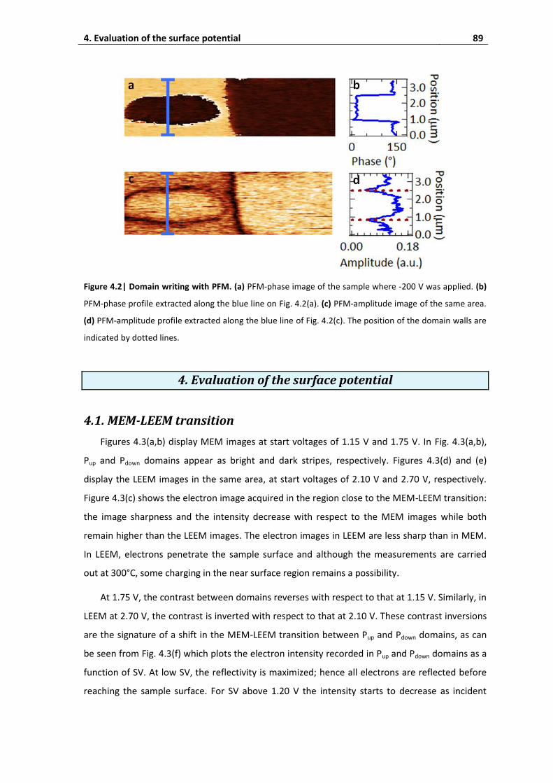
4. Evaluation of the surface potential 89
Figure 4.2| Domain writing with PFM. (a) PFM-phase image of the sample where -200 V was applied. (b)
PFM-phase profile extracted along the blue line on Fig. 4.2(a). (c) PFM-amplitude image of the same area.
(d) PFM-amplitude profile extracted along the blue line of Fig. 4.2(c). The position of the domain walls are
indicated by dotted lines.
4. Evaluation of the surface potential
4.1. MEM-LEEM transition
Figures 4.3(a,b) display MEM images at start voltages of 1.15 V and 1.75 V. In Fig. 4.3(a,b),
Pup and Pdown domains appear as bright and dark stripes, respectively. Figures 4.3(d) and (e)
display the LEEM images in the same area, at start voltages of 2.10 V and 2.70 V, respectively.
Figure 4.3(c) shows the electron image acquired in the region close to the MEM-LEEM transition:
the image sharpness and the intensity decrease with respect to the MEM images while both
remain higher than the LEEM images. The electron images in LEEM are less sharp than in MEM.
In LEEM, electrons penetrate the sample surface and although the measurements are carried
out at 300°C, some charging in the near surface region remains a possibility.
At 1.75 V, the contrast between domains reverses with respect to that at 1.15 V. Similarly, in
LEEM at 2.70 V, the contrast is inverted with respect to that at 2.10 V. These contrast inversions
are the signature of a shift in the MEM-LEEM transition between Pup and Pdown domains, as can
be seen from Fig. 4.3(f) which plots the electron intensity recorded in Pup and Pdown domains as a
function of SV. At low SV, the reflectivity is maximized; hence all electrons are reflected before
reaching the sample surface. For SV above 1.20 V the intensity starts to decrease as incident

90 IV. Low-energy electron imaging of domain walls in lithium niobate
electrons start to have enough energy to overcome the surface potential barrier and penetrate
the sample surface. The domain for which the intensity decreases at lower start voltage has a
lower surface potential, corresponding to the presence of positive surface charge, i.e. an
upwards pointing polarization (Pup)[34,35,92,183]. We can therefore identify the polarization of the
domains, as shown in Fig. 4.3(b). The LEEM and PFM experiments occur in the same area (thanks
to surface defects constituting physical markers) and confirm the polarization deduced from the
two experiments. At SV = 1.60 V, the intensity curves of the Pup and Pdown domains cross giving
rise to contrast inversion in the electron image. The MEM-LEEM transition for Pup (Pdown) is at 1.8
V (1.9 V). The shift in the MEM-LEEM transition between Pup and Pdown domains, and therefore
the difference in surface potential, is ~100 mV.
Figure 4.3| MEM-LEEM transition. MEM images at start voltages of (a) 1.15 V and (b) 1.75 V. Same area
observed in the region close to the MEM-LEEM transition at start voltage of (c) 1.90 V and in LEEM at start
voltages of (d) 2.10 V and (e) 2.70 V. (f) Electron intensity curves extracted from Pup and Pdown domains.
The difference in surface potential can be compared with work functions and surface
potential values obtained on lithium niobate by photoelectron emission microscopy (PEEM) and
electrostatic force microscopy (EFM), respectively.

4. Evaluation of the surface potential 91
The work function (Wf) and surface potential (Sp) contrast should be of the same order but
of opposite sign, as illustrated in Fig. 4.4. Due to Coulomb interactions, electrons are attracted
by positive polarization charges. Thus, electrons from the LEEM gun penetrate in Pup domains
(Fig. 4.4(a)) while photo-electrons generated in PEEM are blocked below the surface (Fig. 4.4(b)).
Respectively, electrons from the LEEM gun are reflected above the surface of Pdown domains
while photo-electrons generated in PEEM overcome the work function barrier of Pdown domains.
This statement has been confirmed experimentally on a BiFeO3 thin film where a work function
difference between Pup and Pdown domains of - 300 mV was found in PEEM and a surface
potential difference of + 450 mV in LEEM[183].
Figure 4.4| Influence of polarization charges on LEEM and PEEM contrasts. Schematic of the interaction
between electrons and ferroelectric domains in (a) LEEM and (b) PEEM.
PEEM measurements on congruent lithium niobate[191] have yielded a work function of
~4.6 V for Pdown domains while that of Pup domains was greater than ~6.2 V, i.e. a work function
contrast difference above 1.6 V, one order of magnitude larger than our value. The surface
potential difference can also be extracted from EFM studies. EFM measurements performed on
stoichiometric lithium niobate in high vacuum were used to study the influence of external
screening charges on the evolution of the surface potential[192]. The contrast was shown to
linearly decrease - and even inverse - with time due the accumulation of screening charges. The
same variations were observed with increasing temperature due to a reduction of polarization
charges through the pyroelectric effect.

92 IV. Low-energy electron imaging of domain walls in lithium niobate
4.2. Influence of screening
The difficulty in comparing experimental values of surface potentials underlines the key role
of screening, even in ultra-high vacuum experiments[31], as previously shown in BaTiO3[34].
However, it is worth noting that a difference of ~100 mV between domains is of the same order
of magnitude as observed in LEEM experiments on BiFeO3[183], Pb(Zr,Ti)O3
[35] and BaTiO3[34].
In order to discuss the screening mechanisms (internal or external) involved at the surface of
lithium niobate, we perform simple calculations based on Maxwell’s equations, as derived by
Kalinin et al.[31]. The surface with periodic 180°-domain structure is approximated by a double-
layer of charges with a height h: a layer of screening charges and a layer of polarization charges,
as shown in Fig. 4.5. The dielectric constant is ε0 above the surface, ε1 between z = 0 and z = -h,
ε2 in the material. In the case of complete screening by adsorbates, ε1 = 80 (permittivity of
water). For internal screening ε1 = ε2.
Figure 4.5| Screening charges for a periodic 180°-domain structure. In the unscreened case, only
polarization charges are at the surface. In the screened case, a double-layer of polarization and screening
charges occupy a height h near the surface.
The potential above the surface, in the double-layer and in the bulk can be written as a
Fourier series, since the domain structure is periodic[31].
In the unscreened case, the surface potential difference between Pup and Pdown domains is:
(4.1)
with
, L = 9.3 μm the domain size, ς = 80 μC/cm2 the surface
charge[175], ε0 the vacuum permittivity, = 31 the average permittivity of lithium
niobate (εe and ε0 are the extraordinary and ordinary permittivity, respectively)[168]. The
calculation gives a surface potential difference of 9748 V, five orders of magnitudes above our

5. Out-of-focus imaging of charged regions 93
experimental value! As this is clearly not possible, the surface charge must be at least partially
screening or the depolarizing field resulting from the surface charge must be compensated.
In the case of a completely screened surface:
(4.2)
where h denotes the height of the double-layer, corresponding to polarization charges and (i)
polar adsorbates above the surface (such as H2O with = 80) or (ii) a depletion layer below the
surface ( = = 31). Using Eq. 4.2, a potential difference of 100 mV between domains is
equivalent to a layer of adsorbates of 0.9 nm or a “skin” depletion layer of 0.4 nm. The former
estimate is reasonable for a molecular adsorbate layer. The latter is also reasonable for a “skin”
layer in a ferroelectric. As order of magnitudes, a “skin” layer of 1-2 nm was found in bismuth
ferrite[193,194]. The main result of the calculation is hence that the surface can be completely
screened. However the main mechanism of screening cannot be identified in this case.
Furthermore, the calculation does not take into account surface and near-surface structural
changes, such as rumpling (height difference between cations and oxygen anions), relaxation
and reconstruction, while it is well known that they occur at virtually all oxide surfaces[195–198].
For example, in BaTiO3, the first four surface atomic layers present rearrangement that reduces
the surface polarization[196]. This rearrangement also change in the presence of adsorbates at the
surface, such as water[197]. Thus, several screening mechanisms can combine to stabilize the
surface.
5. Out-of-focus imaging of charged regions
Usually, MEM-LEEM images are only taken at one focus value. Here, we will show that a
systematic out-of-focus imaging can provide additional information, especially for large band
gap samples. For this, we investigated the intensity contrast further by changing the focus value
of the objective lens at a constant SV = 1.50 V. The results are presented in Fig. 4.6. In LEEM
setup the electron lens are magnetic, the lens setting is therefore measured by the coil current
(mA). The higher the coil current, the stronger the focusing (and the shorter the lens focal
length). In under-focusing conditions, Pdown domains are bright while Pup domains are dark
(Fig. 4.6(a)). If the focus value increases, Pdown domains become darker and increase in size, while
Pup domains become brighter and decrease in size (Fig. 4.6(b) and (c)). At over-focus values, Pup
domains are bright while Pdown domains are dark (Fig. 4.6(c)). The best focus is defined at the coil

94 IV. Low-energy electron imaging of domain walls in lithium niobate
current where the defects appear as white dots surrounded by black circles. This is also the
image with the lowest contrast between domains.
Figure 4.6| Out-of-focus imaging. (a) Under-focus (b) best-focus and (c) over-focus images of the same
area taken at 450°C. (d) Evolution of the domain sizes with focus values expressed in coil current (mA).
Solid lines are linear fit of slope +0.08 μm/mA and -0.07 μm/mA.
Nepijko et al. demonstrated that if the surface potential difference between a negatively
(positively) charged area and a substrate increases, the image size of the charged area increases
(decreases) and its intensity decreases (increases)[94]. This is because the lateral field near the
edge of the charged regions sweeps electrons outwards or inwards, respectively, making the
pattern appear bigger or smaller in the image and as a consequence changing the image
intensity. Varying the objective from under to over focus is similar to varying the surface
potential difference between regions with different surface charge: the higher the surface
potential difference or the further out of focus, the stronger the distortion of the image. The
focusing/defocusing is also responsible for a contrast inversion between Pup and Pdown domains
because the same number of electrons is imaged in a smaller or larger area, changing the
intensities. Note that this does not represent a shift in the MEM-LEEM transition. Simulations

5. Out-of-focus imaging of charged regions 95
show that over-focusing, for an odd number of converging lenses[94], a negatively charged area
(such as Pdown) is dark on the screen[199,200]. Fig. 4.6(c) concurs with simulations.
Figure 4.6(d) shows the evolution of the imaged domain sizes with focusing expressed as
current in the coil of the magnetic lens. The size of the field of view decreases with increasing
focus values; we have therefore calibrated the scale for each focus value by using the distance
between two defects. The domain size in the image changes linearly (straight lines in Fig. 4.6(d))
for the modest changes in focus of a few percent: it decreases for Pup and increases for Pdown. As
a result, the intensity of Pdown decreases with increasing domain size because the same number
of electrons is now spread over a larger area in the image.
Since the variation of domain size depends on the surface charge, it can be used to identify
the domain polarization. This method can therefore be useful to characterize samples with a
large band gap where it is impossible to reach the MEM-LEEM transition because of charging
even at low start voltage. It could also be used to identify the polarization of, for example,
kinetic structures appearing across a phase transition using just two focus values.
Although the focus value changes the intensity contrast between domains, it qualitatively
does not change the MEM-LEEM transition. This can be checked by recording image series as a
function of SV in both under-focusing and over-focusing conditions. The value of the surface
potential for each pixel is then determined by a fit of a complementary error function to the
MEM-LEEM curve. The maps of the surface potential over the full area are shown in Fig. 4.7. The
value found for the surface potential is always lower in Pup domains with respect to Pdown by
~80‐100 mV, irrespective of the focus value, although the absolute values may shift. This makes
the measurement of the surface potential difference between Pup and Pdown robust against slight
(here about 1%) defocusing.
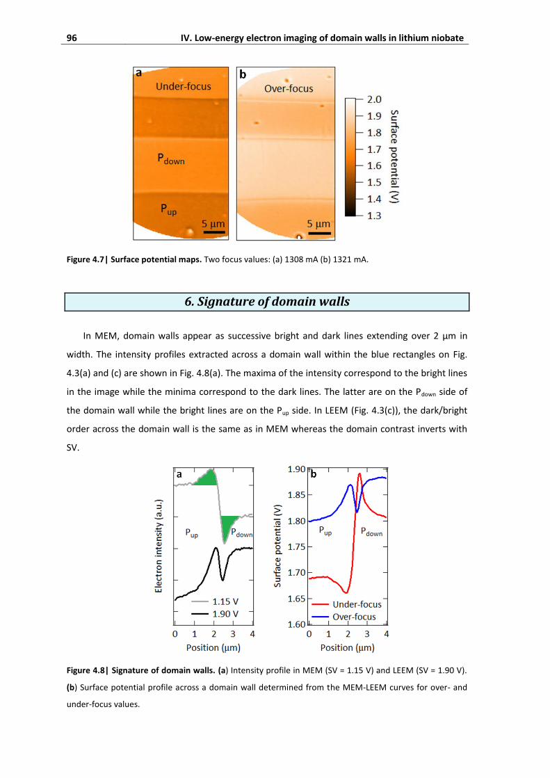
96 IV. Low-energy electron imaging of domain walls in lithium niobate
Figure 4.7| Surface potential maps. Two focus values: (a) 1308 mA (b) 1321 mA.
6. Signature of domain walls
In MEM, domain walls appear as successive bright and dark lines extending over 2 μm in
width. The intensity profiles extracted across a domain wall within the blue rectangles on Fig.
4.3(a) and (c) are shown in Fig. 4.8(a). The maxima of the intensity correspond to the bright lines
in the image while the minima correspond to the dark lines. The latter are on the Pdown side of
the domain wall while the bright lines are on the Pup side. In LEEM (Fig. 4.3(c)), the dark/bright
order across the domain wall is the same as in MEM whereas the domain contrast inverts with
SV.
Figure 4.8| Signature of domain walls. (a) Intensity profile in MEM (SV = 1.15 V) and LEEM (SV = 1.90 V).
(b) Surface potential profile across a domain wall determined from the MEM-LEEM curves for over- and
under-focus values.

6. Signature of domain walls 97
The difference in surface charge between domains gives rise to stray fields, located at
domain walls, as shown in Fig. 4.9. If the stray field is strong enough compared to the extractor
field (6.67 kV/mm) there will be a significant lateral component to the electric field at the point
of electrons take-off and electrons will be deviated from Pdown towards Pup domains, as in Fig.
4.8(a). As a result, near the vicinity of the domain wall, there are fewer electrons in Pdown than in
Pup domains, consistent with the successive changes of intensity where dark lines are near the
Pdown domains.
The deviated electron intensity is represented by the areas below the “bright” peak and the
“dark” peak in green on Fig. 4.8(a). They are approximately equal, consistent with a deviation of
the electrons from the dark to the bright area in a direction parallel to the surface. The fact that
the total number of electrons is conserved shows that at SV = 1.15 V, both areas are still in the
MEM regime.
Figure 4.9| Influence of the lateral electric field. A schematic showing the lateral electric fields developing
at the surface in the vicinity of domain walls and the deviation of the electron beam.
We have also tested the effect of under- and over-focusing on the surface potential contrast
at domain walls. Surface potential inversion occurs when changing from under- to over- focus
conditions, as shown in Fig. 4.7(b) whereas the contrast between Pup and Pdown domains is
qualitatively unchanged far from the domain walls. We believe that the surface potential
contrast inversion at the domain walls is an example of caustic effects. It is due to sharp
variations in electron turning distance from the surface: depending on the local surface
potential, electrons are reflected at a different height above the surface. The rapidly varying
local surface potential changes the z motion of the electrons and therefore the image intensity
in MEM. In particular, if the electron trajectories are strongly modified, electron rays cross and
give rise to very bright features in MEM images known as caustics[199,201]. These changes of
intensity do not have the same magnitude for every SV. Therefore, at domain walls, the
98 IV. Low-energy electron imaging of domain walls in lithium niobate
complementary error function returns a different value for the MEM-LEEM transition as a
function of focusing.
The quantitative difference in surface potential between under- and over-focusing far from
the domain walls is due to the fact that we image charged regions and as discussed with respect
to Fig. 4.6 the intensity changes as a function of focusing and hence the surface potential values.
However, far from the domain wall, there is no rapidly changing value of the local surface
potential and therefore no surface potential contrast inversion with focusing.
LEEM is sensitive to surface physical topography, since it gives rise to local electric fields that
modify the electron trajectories. For example, height differences resulting from differential
etching in ferroelectrics[202] might give rise to intensity contrasts on the screen. Following
Nepijko et al.[94–96] both the aspect ratio and the absolute height difference are important in
determining image intensity. Comparison between Fig. 4.2 (a) and Fig. 4.3(a) already shows that
the smooth variation of height between domains is not observed on the LEEM images where the
domains appears as sharp rectangles with uniform intensity. This ensures that topography plays
a negligible role in contrast formation in the particular case of chemically etched, Mg-doped
lithium niobate.

7. Conclusion 99
7. Conclusion
We used mirror and low energy electron microscopy to carry out a sub-microscopic
characterization of the domains and domain walls at the surface of magnesium-doped lithium
niobate. We showed that the MEM-LEEM transition is a robust way to identify the polarization
of ferroelectric domains and we demonstrated that out of focus settings can be used to
determine the domain polarization.
At domain walls, a local stray, lateral electric field arising from different surface charge
states was observed. This field is measurable as soon as it is strong enough compared to the
extractor field, meaning that LEEM is currently the best technique to study this field. We also
showed that the surface potential contrast at domain walls can be inverted by changing from
under- to over-focusing conditions. We suggest that this is the signature of variations in electron
turning distance due to rapidly varying local surface potential and is an example of caustic
effects.

100 IV. Low-energy electron imaging of domain walls in lithium niobate

101
V. Polar domain walls in calcium titanate
By symmetry, ferroelastic domain walls in calcium titanate are polar. The polarity has been
confirmed by several simulations[75,203,204] and experiments[18,19]. However, these are evidences of
a static polarization at domain walls. Only Salje et al. simulated the dynamics of polarization
when an electric field is applied[20]. They show that the polarization rotates if an electric field
E > 5 kV/mm is applied perpendicular to the initial polarization direction of the domain wall.
Weaker ac-electric fields could lead to mechanical responses of the polar domain walls
through the (inverse) piezoelectric effect. A similar behavior was reported for polar domain walls
in strontium titanate (SrTiO3)[76]. A small ac-voltage was applied across the sample. It induced
oscillations of domain walls, which in turn created local strain fields. These variations of strain
were detected with a piezoelectric transducer.
We have discussed in the previous chapter the surface charge states of ferroelectric domains
and the possible screening mechanisms. Similarly, it is important to identify the surface charge
for different domain walls and to see if it can be externally screened[205].
This chapter is structured as follows: in the first part, the general properties of calcium
titanate are reviewed. In particular, we show how domain walls can be identified by their angle
with respect to specific crystallographic directions. Then, we present a resonant piezoelectric
spectroscopy investigation of a single crystal of calcium titanate with a high density of domain
walls. The goal is to probe the piezoelectric response of polar domain walls. In the last part, we
show the MEM signature of polar domain walls in calcium titanate and its evolution (i) when low
energy electrons are injected into the surface regions and (ii) after annealing. This allows us to
identify the direction of the polarization at domain walls and to investigate the influence of
screening charges.

102 V. Polar domain walls in calcium titanate
1. Calcium titanate
1.1. Structure
Calcium titanate (CaTiO3) undergoes a series of phase transitions from cubic (Pm m) to
tetragonal (I4/mcm) at 1523 K followed by an orthorhombic (Pnma) structure below 1373 –
1423 K[206]. In the high-temperature cubic structure, Ca sits at cube corners positions, Ti at body-
centered positions and O at face-centered positions. The TiO6 octahedra are regular with 90°
angles and six equal Ti-O bonds[206].
At room temperature, the orthorhombic parameters are a = 5.45 Å, b = 7.65 Å and c = 5. 39
Å[206]. The oxygen octahedra are tilted along the three directions of the cubic unit cell, with a tilt
system a-b+a- using Glazer’s notation[207]. This notation traduces equal tilts about [100] and [001]
directions with a different tilt about [010+. The superscript “-” indicates that successive
octahedra along *100+ and *001+ have tilts of opposite signs whereas the superscript “+”
indicates that successive octahedra along [010] have the same tilt. The tilting of the octahedra is
illustrated in Fig. 5.1(a,b). φx- stands for the tilt angle of the octahedron along *100+ and φy
+ for
the tilt angle along [010].
Figure 5.1| Tilt system in calcium titanate. Projections of the crystal structure viewing tilt angles along (a)
the [100] and (b) [010] directions. The blue circles represent Ca atoms. The Ti and O atoms are located at
the center and at each corner of the TiO6 octahedra, respectively. Adapted from [208].
The space group Pnma is centrosymmetric and therefore CaTiO3 is not polar[209]. The
transition from Pm m to Pnma is ferroelastic since it induces a change of crystal family[26].

1. Calcium titanate 103
Therefore, the transition allows the formation of ferroelastic domains in the orthorhombic phase
of CaTiO3, as experimentally observed[210].
1.2. Spontaneous strain tensor
It is convenient to characterize CaTiO3 in the ferroelastic state by the symmetric second-rank
spontaneous strain tensor[26]. The coefficients of this tensor for the transition from Pm m to
Pnma are given by[211]:
(5.1)
(5.2)
(5.3)
(5.4)
where a, b, c are the orthorhombic lattice constants at room temperature. The lattice constant
of the high-symmetry cubic phase a0 is approximated as the average values of the lattice
parameters in the orthorhombic phase[72], i.e.
. Extracting the lattice constants from XRD
data[206], we obtain e11 = -1.2 x 10⁻³, e22 = 5.8 x 10⁻⁴ and e23 = 5.5 x 10⁻³.
Figure 5.2| Orthorombic and pseudocubic axes. Relationship between unit-cell orientation for Pnma
(black) and the reference axes (X,Y,Z) of the Pm m structure (blue). Adapted from [211].
Here spontaneous strains are expressed in the pseudocubic axes. Figure 5.2 shows the
relationships between the orthorhombic axes (x, y, z) and the pseudocubic axes (X, Y, Z). The
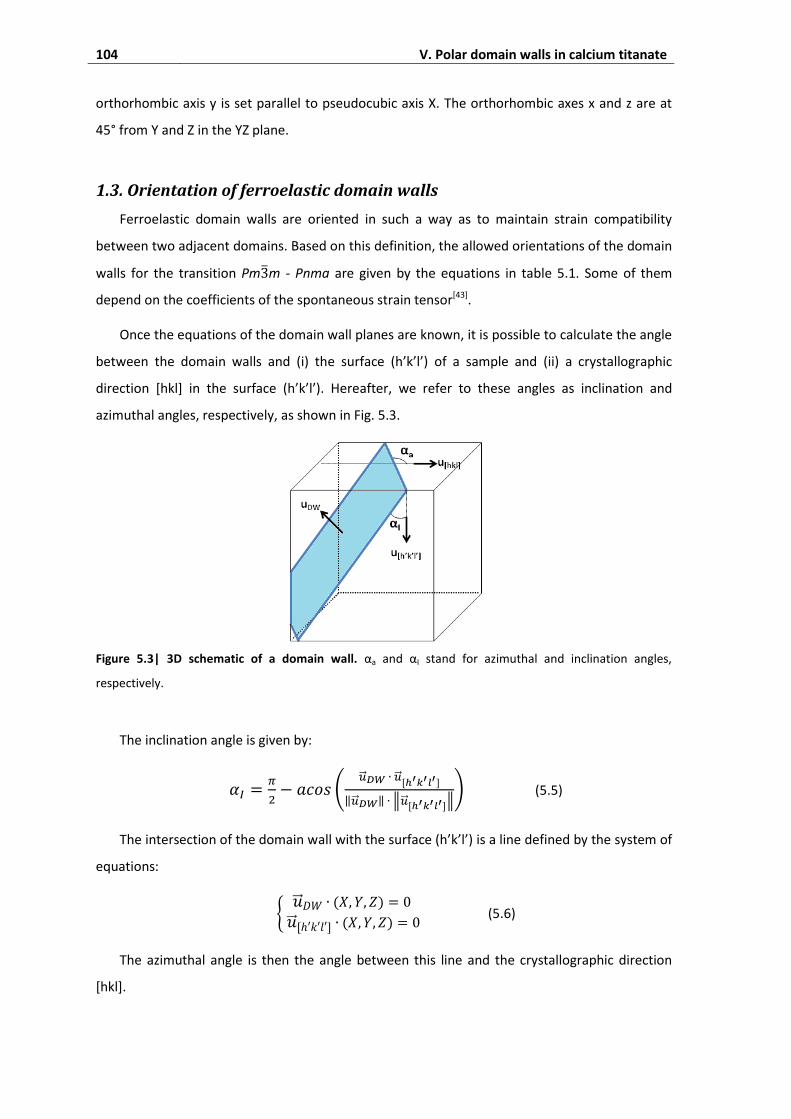
104 V. Polar domain walls in calcium titanate
orthorhombic axis y is set parallel to pseudocubic axis X. The orthorhombic axes x and z are at
45° from Y and Z in the YZ plane.
1.3. Orientation of ferroelastic domain walls
Ferroelastic domain walls are oriented in such a way as to maintain strain compatibility
between two adjacent domains. Based on this definition, the allowed orientations of the domain
walls for the transition Pm m - Pnma are given by the equations in table 5.1. Some of them
depend on the coefficients of the spontaneous strain tensor[43].
Once the equations of the domain wall planes are known, it is possible to calculate the angle
between the domain walls and (i) the surface (h’k’l’) of a sample and (ii) a crystallographic
direction [hkl] in the surface (h’k’l’). Hereafter, we refer to these angles as inclination and
azimuthal angles, respectively, as shown in Fig. 5.3.
Figure 5.3| 3D schematic of a domain wall. αa and αI stand for azimuthal and inclination angles,
respectively.
The inclination angle is given by:
(5.5)
The intersection of the domain wall with the surface (h’k’l’) is a line defined by the system of
equations:
(5.6)
The azimuthal angle is then the angle between this line and the crystallographic direction
[hkl].
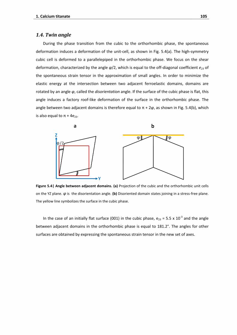
1. Calcium titanate 105
1.4. Twin angle
During the phase transition from the cubic to the orthorhombic phase, the spontaneous
deformation induces a deformation of the unit-cell, as shown in Fig. 5.4(a). The high-symmetry
cubic cell is deformed to a parallelepiped in the orthorhombic phase. We focus on the shear
deformation, characterized by the angle φ/2, which is equal to the off-diagonal coefficient e23 of
the spontaneous strain tensor in the approximation of small angles. In order to minimize the
elastic energy at the intersection between two adjacent ferroelastic domains, domains are
rotated by an angle φ, called the disorientation angle. If the surface of the cubic phase is flat, this
angle induces a factory roof-like deformation of the surface in the orthorhombic phase. The
angle between two adjacent domains is therefore equal to π + 2φ, as shown in Fig. 5.4(b), which
is also equal to π + 4e23.
Figure 5.4| Angle between adjacent domains. (a) Projection of the cubic and the orthorhombic unit cells
on the YZ plane. φ is the disorientation angle. (b) Disoriented domain states joining in a stress-free plane.
The yellow line symbolizes the surface in the cubic phase.
In the case of an initially flat surface (001) in the cubic phase, e23 = 5.5 x 10⁻³ and the angle
between adjacent domains in the orthorhombic phase is equal to 181.2°. The angles for other
surfaces are obtained by expressing the spontaneous strain tensor in the new set of axes.
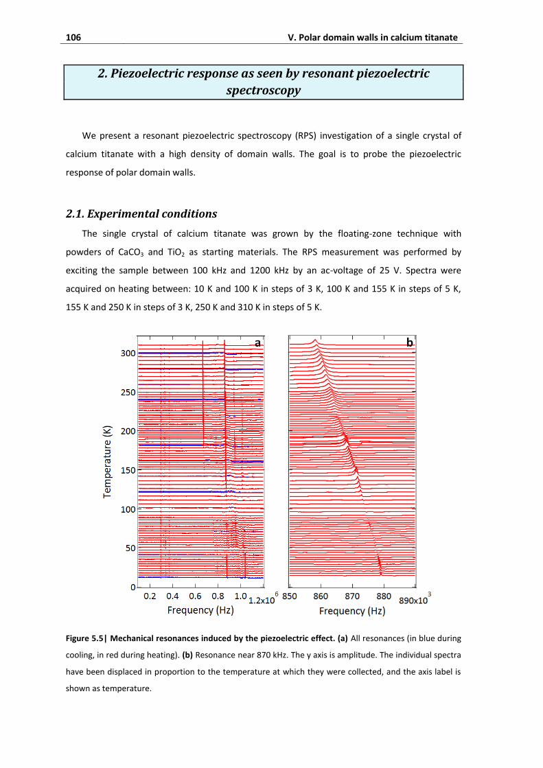
106 V. Polar domain walls in calcium titanate
2. Piezoelectric response as seen by resonant piezoelectric
spectroscopy
We present a resonant piezoelectric spectroscopy (RPS) investigation of a single crystal of
calcium titanate with a high density of domain walls. The goal is to probe the piezoelectric
response of polar domain walls.
2.1. Experimental conditions
The single crystal of calcium titanate was grown by the floating-zone technique with
powders of CaCO3 and TiO2 as starting materials. The RPS measurement was performed by
exciting the sample between 100 kHz and 1200 kHz by an ac-voltage of 25 V. Spectra were
acquired on heating between: 10 K and 100 K in steps of 3 K, 100 K and 155 K in steps of 5 K,
155 K and 250 K in steps of 3 K, 250 K and 310 K in steps of 5 K.
Figure 5.5| Mechanical resonances induced by the piezoelectric effect. (a) All resonances (in blue during
cooling, in red during heating). (b) Resonance near 870 kHz. The y axis is amplitude. The individual spectra
have been displaced in proportion to the temperature at which they were collected, and the axis label is
shown as temperature.
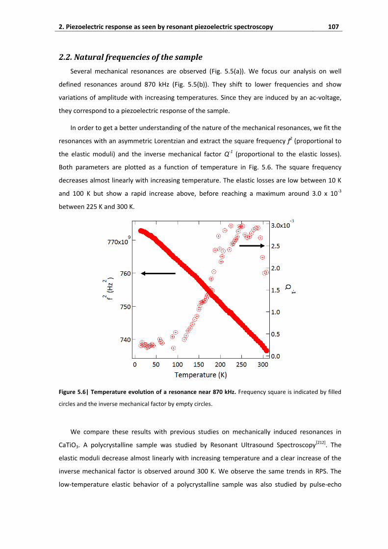
2. Piezoelectric response as seen by resonant piezoelectric spectroscopy 107
2.2. Natural frequencies of the sample
Several mechanical resonances are observed (Fig. 5.5(a)). We focus our analysis on well
defined resonances around 870 kHz (Fig. 5.5(b)). They shift to lower frequencies and show
variations of amplitude with increasing temperatures. Since they are induced by an ac-voltage,
they correspond to a piezoelectric response of the sample.
In order to get a better understanding of the nature of the mechanical resonances, we fit the
resonances with an asymmetric Lorentzian and extract the square frequency f2 (proportional to
the elastic moduli) and the inverse mechanical factor Q-1 (proportional to the elastic losses).
Both parameters are plotted as a function of temperature in Fig. 5.6. The square frequency
decreases almost linearly with increasing temperature. The elastic losses are low between 10 K
and 100 K but show a rapid increase above, before reaching a maximum around 3.0 x 10⁻³
between 225 K and 300 K.
Figure 5.6| Temperature evolution of a resonance near 870 kHz. Frequency square is indicated by filled
circles and the inverse mechanical factor by empty circles.
We compare these results with previous studies on mechanically induced resonances in
CaTiO3. A polycrystalline sample was studied by Resonant Ultrasound Spectroscopy[212]. The
elastic moduli decrease almost linearly with increasing temperature and a clear increase of the
inverse mechanical factor is observed around 300 K. We observe the same trends in RPS. The
low-temperature elastic behavior of a polycrystalline sample was also studied by pulse-echo
108 V. Polar domain walls in calcium titanate
ultrasonic technique[213]. Longitudinal and transverse ultrasound velocities are proportional to
the frequency of RPS resonances: they decrease almost linearly with increasing temperature.
The attenuation coefficient is proportional to the inverse mechanical factor of the RPS
resonances: they both increase above 100 K. The mechanical resonances excited by the
piezoelectric effect in RPS are therefore similar to the mechanically induced resonances. This is a
strong indication of the reproducibility of the measurements. However, since CaTiO3 is not
piezoelectric[75] the natural frequencies of the sample cannot be directly excited by the ac-
voltage.
2.3. Oscillation of polar domain walls
Piezoelectric excitations of the natural frequencies of ferroelastic or non-ferroelectric
samples have been already explained by several mechanisms:
(i) In SrTiO3, the applied ac-voltage leads to the oscillation of polar domain walls
through the piezoelectric effect, which creates strain fields around domain walls[76].
The resulting elastic wave becomes resonant if its frequency corresponds to a
natural frequency of the sample. This mechanical resonance condition enhances
considerably the amplitude of the elastic wave and explains why RPS is sensitive to
domain walls, even if they represent only a small fraction of the sample.
(ii) In the incipient ferroelectric (non-ferroelastic) KTaO3, defects are polars. At high
temperatures they are randomly oriented and not detected with RPS[214]. With
decreasing temperature, switchable defect dipoles freeze in parallel arrangements
and induce macroscopic polarity. This polarity is accompanied by an increase of the
piezoelectricity. The ac-voltage applied induces a coherent movement of these
dipoles and gives rise to a RPS signal.
(iii) In the cubic phase of BaTiO3, the applied voltage interacts with piezoelectric regions
inside a precursor structure and generates mechanical resonances[102]. This
microstructure corresponds to dynamic tweed. The same mechanism is used to
explain the presence of RPS resonances in the cubic phase of Pb(Sc,Ta)O3[102].
Tweed and polar defect structures have not been reported in the literature on CaTiO3.
Therefore, given the experimental evidences for polar domain walls in CaTiO3[18,19], it is likely
that the RPS resonances are induced by polar - and hence piezoelectric - domain walls, as
described in mechanism (i). However, the exact domain walls response to the electric field
cannot be deduced from our experiment. It can correspond to a lateral movement of the

2. Piezoelectric response as seen by resonant piezoelectric spectroscopy 109
domain walls, a tilting out of their normal crystallographic plane, an advance/retraction of a
needle domain or local bowing, as previously discussed in LaAlO3[215].
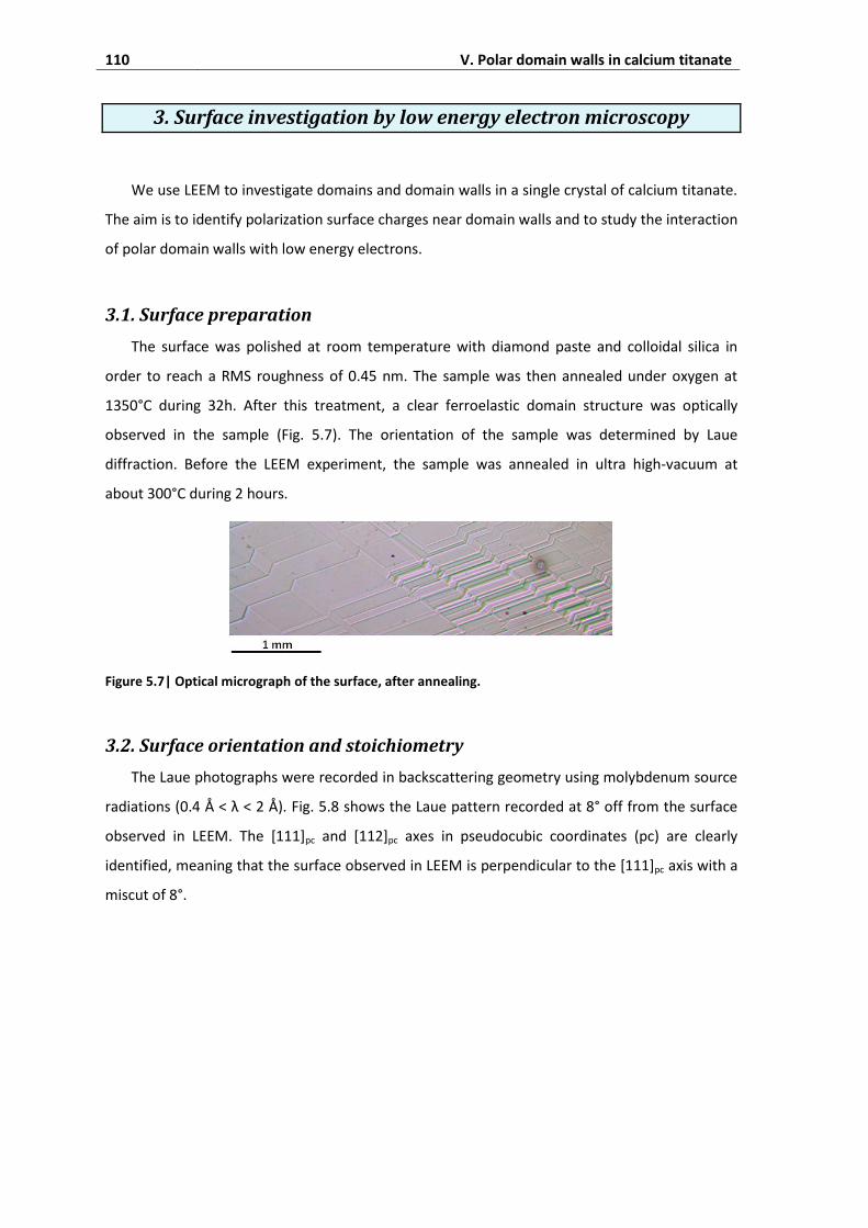
110 V. Polar domain walls in calcium titanate
3. Surface investigation by low energy electron microscopy
We use LEEM to investigate domains and domain walls in a single crystal of calcium titanate.
The aim is to identify polarization surface charges near domain walls and to study the interaction
of polar domain walls with low energy electrons.
3.1. Surface preparation
The surface was polished at room temperature with diamond paste and colloidal silica in
order to reach a RMS roughness of 0.45 nm. The sample was then annealed under oxygen at
1350°C during 32h. After this treatment, a clear ferroelastic domain structure was optically
observed in the sample (Fig. 5.7). The orientation of the sample was determined by Laue
diffraction. Before the LEEM experiment, the sample was annealed in ultra high-vacuum at
about 300°C during 2 hours.
Figure 5.7| Optical micrograph of the surface, after annealing.
3.2. Surface orientation and stoichiometry
The Laue photographs were recorded in backscattering geometry using molybdenum source
radiations (0.4 Å < λ < 2 Å). Fig. 5.8 shows the Laue pattern recorded at 8° off from the surface
observed in LEEM. The [111]pc and [112]pc axes in pseudocubic coordinates (pc) are clearly
identified, meaning that the surface observed in LEEM is perpendicular to the [111]pc axis with a
miscut of 8°.
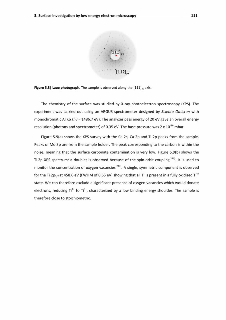
3. Surface investigation by low energy electron microscopy 111
Figure 5.8| Laue photograph. The sample is observed along the [111]pc axis.
The chemistry of the surface was studied by X-ray photoelectron spectroscopy (XPS). The
experiment was carried out using an ARGUS spectrometer designed by Scienta Omicron with
monochromatic Al Kα (hν = 1486.7 eV). The analyzer pass energy of 20 eV gave an overall energy
resolution (photons and spectrometer) of 0.35 eV. The base pressure was 2 x 10⁻¹⁰ mbar.
Figure 5.9(a) shows the XPS survey with the Ca 2s, Ca 2p and Ti 2p peaks from the sample.
Peaks of Mo 3p are from the sample holder. The peak corresponding to the carbon is within the
noise, meaning that the surface carbonate contamination is very low. Figure 5.9(b) shows the
Ti 2p XPS spectrum: a doublet is observed because of the spin-orbit coupling[216]. It is used to
monitor the concentration of oxygen vacancies[217]. A single, symmetric component is observed
for the Ti 2p3/2 at 458.6 eV (FWHM of 0.65 eV) showing that all Ti is present in a fully oxidized Ti4+
state. We can therefore exclude a significant presence of oxygen vacancies which would donate
electrons, reducing Ti4+ to Ti3+, characterized by a low binding energy shoulder. The sample is
therefore close to stoichiometric.
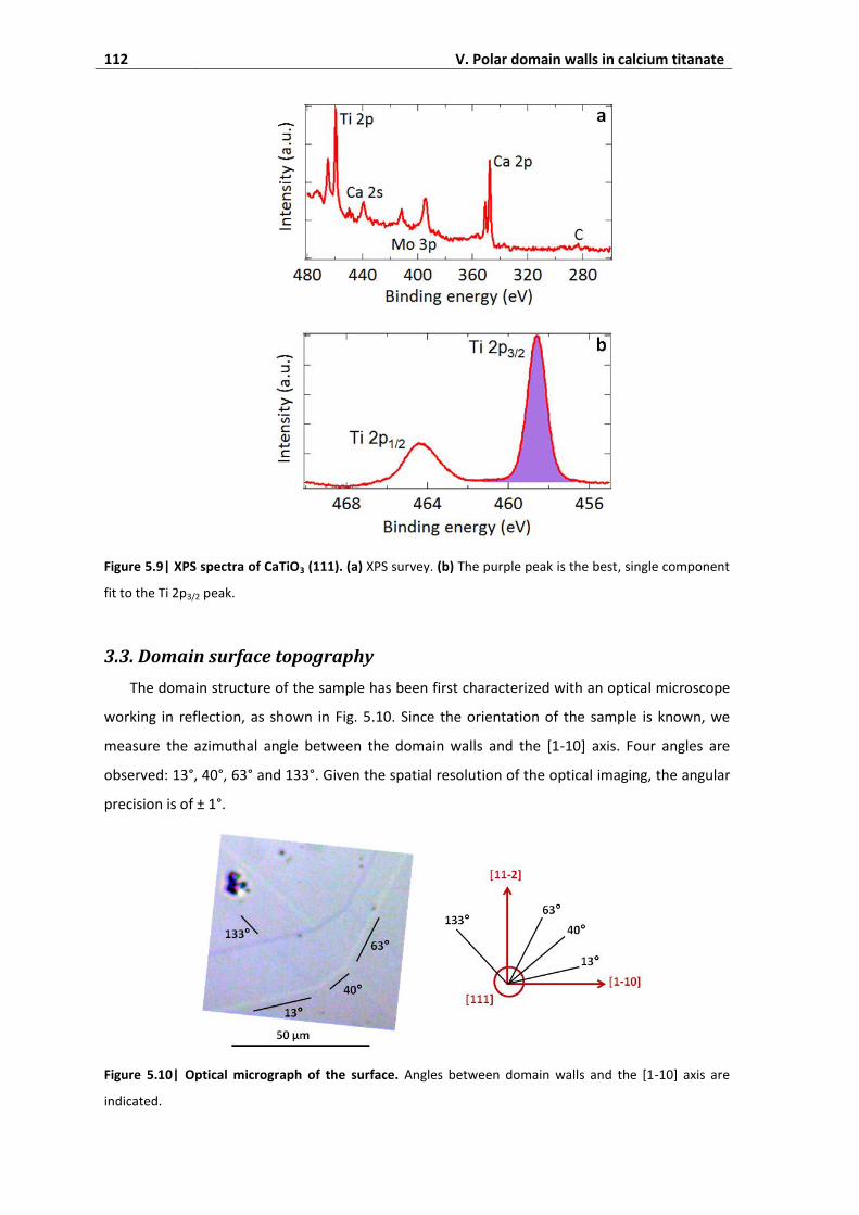
112 V. Polar domain walls in calcium titanate
Figure 5.9| XPS spectra of CaTiO3 (111). (a) XPS survey. (b) The purple peak is the best, single component
fit to the Ti 2p3/2 peak.
3.3. Domain surface topography
The domain structure of the sample has been first characterized with an optical microscope
working in reflection, as shown in Fig. 5.10. Since the orientation of the sample is known, we
measure the azimuthal angle between the domain walls and the [1-10] axis. Four angles are
observed: 13°, 40°, 63° and 133°. Given the spatial resolution of the optical imaging, the angular
precision is of ± 1°.
Figure 5.10| Optical micrograph of the surface. Angles between domain walls and the [1-10] axis are
indicated.

3. Surface investigation by low energy electron microscopy 113
Figure 5.11 shows a 3D landscape acquired by atomic force microscopy (AFM). The valleys
(V) and ridges (R) of the domain structure appear clearly. The dots are surface contamination
which are usefull for alignment but have no influence on the domain wall polarity. We identify
five domain walls that are studied further with MEM and LEEM: ridges R1 and R2 and valleys V1,
V2 and V3. The left and right hand insets show height profiles along the red (R2) and blue (V3)
horizontal lines on the main image, respectively. The red (ridge) profile shows a 180.4° twin
angle, whereas the valley is at 179.7°. Other angles are found in the range 179.4° to 180.5°.
These values differ slightly from the theoretical angles calculated for a (111) surface: 179.9° (or
180.1°) and 179.2° (or 180.8°). This calculation is based on the equations of section 1.4 for the
set of axes [111], [1-10] and [11-2], as indicated in Fig. 5.10. The calculation assumes that the
high-temperature cubic surface is flat. However, since we performed the polishing at room
temperature, in the orthorhombic phase, this is probably not the case.
Figure 5.11| AFM topography of the sample surface. The valleys and ridges of the domain walls are
labeled “V” and “R”, respectively. The left-hand inset shows the height profile perpendicular to the R2
ridge, the right-hand inset the V3 height profile.
3.4. Electron imaging of domain walls
Figure 5.12 shows typical MEM images of the same area as the AFM landscape, taken at
start voltages of (a) - 0.8 V and (b) + 0.3 V. There are three main features in both images. First,
the electron intensity on either side of the domain walls is the same, indicating identical surface
potentials. Second, the surface contamination in the form of nanoparticles appears as white
dots. These particles actually provide an internal benchmark allowing distinguishing the best
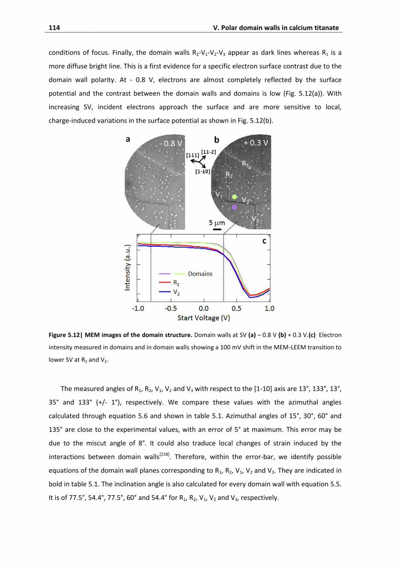
114 V. Polar domain walls in calcium titanate
conditions of focus. Finally, the domain walls R2-V1-V2-V3 appear as dark lines whereas R1 is a
more diffuse bright line. This is a first evidence for a specific electron surface contrast due to the
domain wall polarity. At - 0.8 V, electrons are almost completely reflected by the surface
potential and the contrast between the domain walls and domains is low (Fig. 5.12(a)). With
increasing SV, incident electrons approach the surface and are more sensitive to local,
charge‐induced variations in the surface potential as shown in Fig. 5.12(b).
Figure 5.12| MEM images of the domain structure. Domain walls at SV (a) – 0.8 V (b) + 0.3 V.(c) Electron
intensity measured in domains and in domain walls showing a 100 mV shift in the MEM-LEEM transition to
lower SV at R2 and V2.
The measured angles of R1, R2, V1, V2 and V3 with respect to the [1-10] axis are 13°, 133°, 13°,
35° and 133° (+/- 1°), respectively. We compare these values with the azimuthal angles
calculated through equation 5.6 and shown in table 5.1. Azimuthal angles of 15°, 30°, 60° and
135° are close to the experimental values, with an error of 5° at maximum. This error may be
due to the miscut angle of 8°. It could also traduce local changes of strain induced by the
interactions between domain walls[218]. Therefore, within the error-bar, we identify possible
equations of the domain wall planes corresponding to R1, R2, V1, V2 and V3. They are indicated in
bold in table 5.1. The inclination angle is also calculated for every domain wall with equation 5.5.
It is of 77.5°, 54.4°, 77.5°, 60° and 54.4° for R1, R2, V1, V2 and V3, respectively.

3. Surface investigation by low energy electron microscopy 115
Name Equation Azimuthal angle (°) Inclination angle (°)
x = 0 120 35.3
y = 0 120 35.3
z = 0 0 35.3
x = y 90 0
x = -y 0 54.7
V2 y = z 150 0
y = -z 60 54.7
V2 z = x 150 0
z = -x 60 54.7
3e11(z+x ) + e12y = 0 120 47.7
3e11(z+x) - e12y = 0 60 22.9
3e11(z-x) + e12y = 0 104.9 34.3
R2, V3 3e11(z-x) - e12y = 0 44.9 34.3
3e11(x+y) + e12z = 0 0 47.7
3e11(x+y) - e12z = 0 0 22.9
R1, V1 3e11(x-y) - e12z = 0 164.9 34.3
R1, V1 3e11(x-y) + e12z = 0 15.1 34.3
3e11(y+z) + e12x = 0 120 47.7
3e11(y+z) - e12x = 0 60 22.9
R2, V3 3e11(y-z) + e12x = 0 135.1 34.3
3e11(y-z) - e12x = 0 75.1 34.3 Table 5.1| Calculated parameters of domain walls. Domain walls equations, azimuthal angles with
respect to the [1-10] direction and inclination angles with respect to the (111) surface.
The contrast at domain walls is defined as:
(5.7)
where Idomain wall and Idomain are the intensities at DWs and inside domains, respectively. The
magnitude, , is different for each domain walls. In particular it is three times higher at R2, V2
and V3 ( ) than at R1 and V1 ( . Correlation with, for example, the
inclination angle is not, however, straightforward, as shown in table 5.2.
Figure 5.12(c) plots the electron intensity from the domains and from the domain walls as a
function of SV. The MEM-LEEM transition occurs at exactly the same SV value in both domains
(green and mauve dots) showing that they have the same surface potential. At the R2-V2-V3
domain walls the MEM-LEEM transition occurs at lower (about 100 mV) SV which is a signature
of a positive surface charge.

116 V. Polar domain walls in calcium titanate
Name Type Azimuthal angle (°)
Calculated inclination angle (°)
Factory-roof angle (°)
Contrast
R1 Ridge 13 34.3 180.5 + 3.6 ∙ 10-2
R2 Ridge 133 34.3 180.4 - 7.6 ∙ 10-2
V1 Valley 13 34.3 179.4 - 2.2 ∙ 10-2
V2 Valley 35 0 179.5 - 1.1 ∙ 10-1
V3 Valley 133 34.3 179.7 - 7.4 ∙ 10-2 Table 5.2| Main results obtained on R1, R2, V1, V2 and V3. Azimuthal angles measured on the MEM image,
calculated inclination angles, factory-roof angles measured with AFM, contrast in MEM.
3.6. Under and over-focusing
We now study in details the high contrast observed at R2 and V2. Figure 5.13(a) shows a
MEM image obtained at SV = 0.3 V with a Field of View of 14 μm. Two domain walls are easily
visible: R2 and V2. We have shown in chapter IV (section 5) that the sign of a charged surface can
be quickly identified by out-of-focus imaging. Figures 5.13(a,b,c) are MEM images obtained at
SV = 0.3 V for three different focusing conditions. The best focus is defined as the focus where
the dots due to surface contamination are faint and appear as white dots inside black disks
(Fig. 5.13(b)). Going from under-focus to over-focus conditions, the contrast at domain walls
goes from negative to positive values and the bright dots become dark. This is the signature of a
positive surface charge.
Figure 5.13| MEM images of R2 and V2. Images at (a) under-focus (b) best-focus and (c) over-focus.
(d)-(f) Profiles across R2 for different focus conditions. (g)-(i) Profiles across V2 for different focus
conditions. The profiles have been averaged on the rectangles indicated in (a).
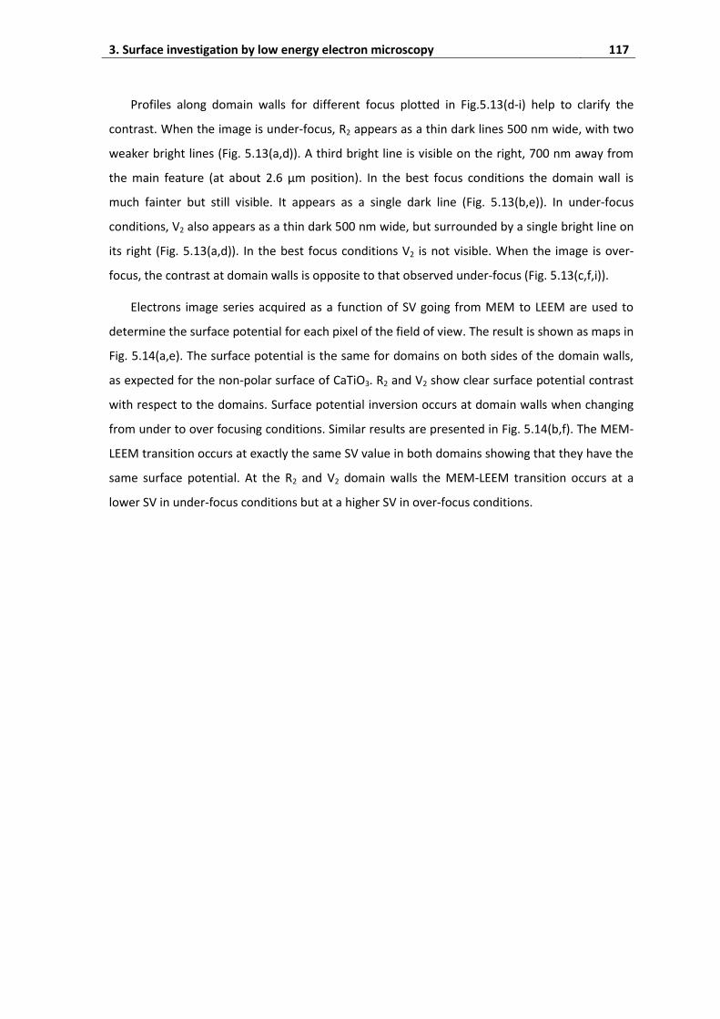
3. Surface investigation by low energy electron microscopy 117
Profiles along domain walls for different focus plotted in Fig.5.13(d-i) help to clarify the
contrast. When the image is under-focus, R2 appears as a thin dark lines 500 nm wide, with two
weaker bright lines (Fig. 5.13(a,d)). A third bright line is visible on the right, 700 nm away from
the main feature (at about 2.6 μm position). In the best focus conditions the domain wall is
much fainter but still visible. It appears as a single dark line (Fig. 5.13(b,e)). In under-focus
conditions, V2 also appears as a thin dark 500 nm wide, but surrounded by a single bright line on
its right (Fig. 5.13(a,d)). In the best focus conditions V2 is not visible. When the image is over-
focus, the contrast at domain walls is opposite to that observed under-focus (Fig. 5.13(c,f,i)).
Electrons image series acquired as a function of SV going from MEM to LEEM are used to
determine the surface potential for each pixel of the field of view. The result is shown as maps in
Fig. 5.14(a,e). The surface potential is the same for domains on both sides of the domain walls,
as expected for the non-polar surface of CaTiO3. R2 and V2 show clear surface potential contrast
with respect to the domains. Surface potential inversion occurs at domain walls when changing
from under to over focusing conditions. Similar results are presented in Fig. 5.14(b,f). The MEM-
LEEM transition occurs at exactly the same SV value in both domains showing that they have the
same surface potential. At the R2 and V2 domain walls the MEM-LEEM transition occurs at a
lower SV in under-focus conditions but at a higher SV in over-focus conditions.
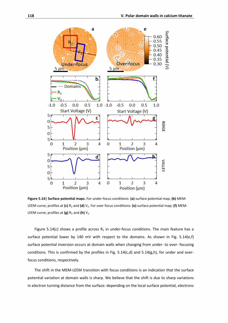
118 V. Polar domain walls in calcium titanate
Figure 5.14| Surface potential maps. For under-focus conditions: (a) surface potential map; (b) MEM-
LEEM curve; profiles at (c) R2 and (d) V2. For over-focus conditions: (e) surface potential map; (f) MEM-
LEEM curve; profiles at (g) R2 and (h) V2.
Figure 5.14(c) shows a profile across R2 in under-focus conditions. The main feature has a
surface potential lower by 140 mV with respect to the domains. As shown in Fig. 5.14(e,f)
surface potential inversion occurs at domain walls when changing from under- to over- focusing
conditions. This is confirmed by the profiles in Fig. 5.14(c,d) and 5.14(g,h), for under and over-
focus conditions, respectively.
The shift in the MEM-LEEM transition with focus conditions is an indication that the surface
potential variation at domain walls is sharp. We believe that the shift is due to sharp variations
in electron turning distance from the surface: depending on the local surface potential, electrons
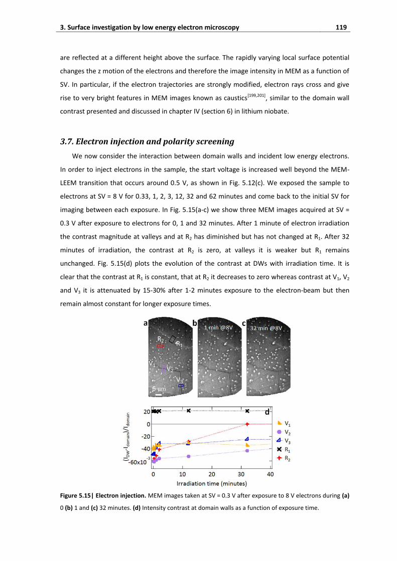
3. Surface investigation by low energy electron microscopy 119
are reflected at a different height above the surface. The rapidly varying local surface potential
changes the z motion of the electrons and therefore the image intensity in MEM as a function of
SV. In particular, if the electron trajectories are strongly modified, electron rays cross and give
rise to very bright features in MEM images known as caustics[199,201], similar to the domain wall
contrast presented and discussed in chapter IV (section 6) in lithium niobate.
3.7. Electron injection and polarity screening
We now consider the interaction between domain walls and incident low energy electrons.
In order to inject electrons in the sample, the start voltage is increased well beyond the MEM-
LEEM transition that occurs around 0.5 V, as shown in Fig. 5.12(c). We exposed the sample to
electrons at SV = 8 V for 0.33, 1, 2, 3, 12, 32 and 62 minutes and come back to the initial SV for
imaging between each exposure. In Fig. 5.15(a-c) we show three MEM images acquired at SV =
0.3 V after exposure to electrons for 0, 1 and 32 minutes. After 1 minute of electron irradiation
the contrast magnitude at valleys and at R2 has diminished but has not changed at R1. After 32
minutes of irradiation, the contrast at R2 is zero, at valleys it is weaker but R1 remains
unchanged. Fig. 5.15(d) plots the evolution of the contrast at DWs with irradiation time. It is
clear that the contrast at R1 is constant, that at R2 it decreases to zero whereas contrast at V1, V2
and V3 it is attenuated by 15-30% after 1-2 minutes exposure to the electron-beam but then
remain almost constant for longer exposure times.
Figure 5.15| Electron injection. MEM images taken at SV = 0.3 V after exposure to 8 V electrons during (a)
0 (b) 1 and (c) 32 minutes. (d) Intensity contrast at domain walls as a function of exposure time.
120 V. Polar domain walls in calcium titanate
We can estimate the number of electrons (Ne) injected in the sample through the beam spot
by assuming Ne is the difference between the number of incident and detected electrons and
that the reflectivity at very negative SV is unity. At the MEM-LEEM transition electrons penetrate
the sample surface and the reflectivity R decreases since electrons can be absorbed and/or
scattered. For an electron gun current Ie of 20 nA, an irradiation time t, the number of electrons
is:
(5.8)
where e is the charge of the electron. After 1 minute of irradiation at SV = 8 V, we estimate
that 3.5 x 10¹² electrons have been injected. After 32 minutes, 1.1 x 10¹⁴ electrons have been
injected. However, in the absence of an accurate drain current measurement this is only an
estimate. Indeed, above SV = 3.75 V the reflectivity increases linearly, as shown in Fig. 5.16. This
is an indication that the sample is charging. Indeed, in contrast to keV electrons, the inelastic
mean free path (λ) of very low energy electrons (< 10 eV) decreases with increasing kinetic
energies[219]: thus as SV increases but remains very low in energy, the electron mean free path
decreases, the electrons accumulate at the surface, and hence reflectivity increases. For the
calculation, we consider that the true reflectivity above SV = 3.75 V is constant.
Figure 5.16| MEM-LEEM curve in a domain. Above 3.75 V, the reflectivity increases linearly.
Following Cazaux[219] and Ziaja[220], we estimate the inelastic mean free path of the electrons
at 8 V to be 5-10 nm. For a circular beam spot of diameter d = 90 μm, if the electrons
penetration depth is 3λ, the charge density (ρ) is given by:
(5.9)
The electron injection at SV = 8 V during 32 minutes corresponds then to a charge density of
5.8 x 1029 e/m3. This figure is actually 6 orders of magnitude higher than the injected charged

3. Surface investigation by low energy electron microscopy 121
used to switch ferroelectric and ferroelastic domains in BaTiO3 in a transmission electron
microscope[221].
In Fig. 5.17(a-c) we show images acquired at SV = 0.3 V after exposure to electrons during 10
minutes with different start voltages. At higher SV more electrons are expected to penetrate
into the sample, at the same time the inelastic mean free path decreases, increasing the injected
charge density. After a 6 V irradiation, the absolute contrast at V1, V2, V3 and R2 has diminished
but has not changed at R1. After a 10 V irradiation, the contrast at V1, V2, V3 and R2 is almost null,
whereas the contrast at R1 has not changed. The spots due to surface contamination are
brighter, probably due to slight charging under the electron-beam.
Figure 5.17| Electron injection at different SV. MEM images (a) before electron injection, after exposure
to electrons at (b) SV = 6 V and (c) SV = 10 V during 10 minutes.
3.8. Reversibility of polarity screening
It is possible to recover the initial state of Fig. 5.15(a), i.e. the one before charge injection, by
annealing the sample in-situ above 250°C. The electron images after 10 minutes exposure to
20 V electrons are shown in Figure 5.18(a-c) for the intersections R1-R2, R2-V1-V2 and V2-V3. The
contrast at all positive polarity domain walls is weak after electron injection, only R1 is clearly
distinguishable. Fig 5.18(d-f) shows the same regions after annealing at 330°C. Contrast at R2, V1,
V2 and V3 has been fully recovered and the contrast at R1 is still present. The temperature
dependence of the contrast recovery is shown in Fig 5.18(g). Up to 100°C there is no change, and
then above 100°C the contrast slowly reappears. It then stays even after the sample is cooled
down to room temperature. This is strong evidence that screening of the domain wall contrast is
achieved by injected electrons forming a space charge region around positive polarity domain
walls. Charge dissipation must be thermally activated. Importantly, annealing up to 330°C not
only leaves the domain walls in the same position it also does not change their polarity. The wall
memory is therefore robust at least up to 330°C. We note that the double, nearly vertical lines in
Fig. 5.18(c) and (f) are scratches, not domain walls.

122 V. Polar domain walls in calcium titanate
Figure 5.18| Influence of temperature. MEM images acquired at SV = 0.3 V after 10 minutes exposure to
20 V electron-beam: the intersections (a) R1-R2,(b) R2-V1-V2 and (c) V2-V3. (d-f) Same regions imaged at
room temperature after annealing at 330°C. (g) Intensity contrast at R2 and V3 as a function of
temperature.
3.9. Discussion
As shown in Fig. 5.12(a), all domain walls are visible in MEM. For ridges, two contrasts with
surrounding domains are observed: positive for R1 and negative for R2. If the contrast at domain
walls were due to the ridge topography it should have the same sign for all ridges. Indeed, in
MEM, an asperity on the surface causes a local electric field perturbation that deviates incident
and reflected electrons. The direction of the deviation depends on the geometry of the asperity:
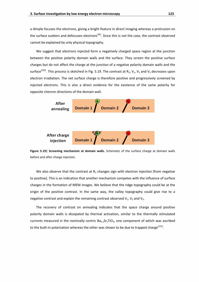
3. Surface investigation by low energy electron microscopy 123
a dimple focuses the electrons, giving a bright feature in direct imaging whereas a protrusion on
the surface scatters and defocuses electrons[95]. Since this is not the case, the contrast observed
cannot be explained by only physical topography.
We suggest that electrons injected form a negatively charged space region at the junction
between the positive polarity domain walls and the surface. They screen the positive surface
charges but do not affect the charge at the junction of a negative polarity domain walls and the
surface[205]. This process is sketched in Fig. 5.19. The contrast at R2, V1, V2 and V3 decreases upon
electron irradiation. The net surface charge is therefore positive and progressively screened by
injected electrons. This is also a direct evidence for the existence of the same polarity for
opposite chevron directions of the domain wall.
Figure 5.19| Screening mechanism at domain walls. Schematic of the surface charge at domain walls
before and after charge injection.
We also observe that the contrast at R2 changes sign with electron injection (from negative
to positive). This is an indication that another mechanism competes with the influence of surface
charges in the formation of MEM images. We believe that the ridge topography could be at the
origin of the positive contrast. In the same way, the valley topography could give rise to a
negative contrast and explain the remaining contrast observed V1, V2 and V3.
The recovery of contrast on annealing indicates that the space charge around positive
polarity domain walls is dissipated by thermal activation, similar to the thermally stimulated
currents measured in the nominally centric Ba1-xSrxTiO3, one component of which was ascribed
to the built-in polarization whereas the other was shown to be due to trapped charge[222].
124 V. Polar domain walls in calcium titanate
4. Conclusions on polar domain walls
We first investigated the polarity of domain walls in calcium titanate by resonant
piezoelectric spectroscopy. We reported mechanical excitations induced by an ac-electric field,
i.e a piezoelectric effect. Since the space group of calcium titanate does not allow
piezoelectricity, we attributed this effect to polar domain walls. This would be then a first
experimental evidence for an electric (here rather electromechanical) response of the domain
walls.
A direct image of the polar domain walls was obtained by LEEM. As expected, adjacent
domains presented the same surface potential because the material is non-polar. On the other
hand, the domain walls showed a clear surface potential contrast with respect to the domains.
This result strengthens the previous observations of polar domain walls and shows that the
polarity is still measurable at the surface. We also observed that the contrast between domains
and domain walls changes upon electron irradiation. Electrons injected form a negatively
charged space region at the surface. They screen the positive surface charges without affecting
the negative ones, both arising from the polarization of the domain walls. It is possible to
recover the initial state, i.e. before charge injection, by annealing above 250°C.
125
Conclusion
Summary
The structural and electronic properties of domain walls were investigated to achieve a
better understanding of the mechanisms behind the conduction within domain walls of lithium
niobate and the polarity of domain walls in calcium titanate.
The first part of this thesis discusses the interaction between defects and domain walls in
lithium niobate. Monodomain and periodically poled congruent lithium niobate crystals were
investigated by dielectric spectroscopy. A resonance was observed near 30 kHz. This resonance
vanished under thermal anneal in monodomain samples while it remained stable in periodically
poled samples where the density of domain walls is high. The low activation energy of the
resonance suggests its electronic origin. We therefore propose that domain walls stabilize
polaronic states with (bi-)polarons located inside or near domain walls.
This result proves the benefit of studying ferroelectric non-ferroelastic domain walls using
dielectric spectroscopy, even though it is a macroscopic technique.
The domain structure of lithium niobate was also investigated by Raman spectroscopy
mapping. We reported the evolution of E(TO1), E(TO8) and A1(LO4) Raman modes with
increasing amount of magnesium in congruent lithium niobate. We observed contrasts between
virgin and reversed domains, consistent with the literature and identified other frequency shifts
of the Raman modes at the domain walls. The information gained from the systematic study of
the role of magnesium concentrations, before and after annealing, allows us to probe
differences between the signatures of polar defects in the bulk and at the domain walls. The
domains walls appear then as regions where polar defects are stabilized. Since the frequency
shifts at domain walls remain the same under illumination, we conclude that UV-light does not,
significantly, influence the structure of the polar defects and the strain around domain walls.
All our results indicate that 180°-domain walls in lithium niobate are preferential locations
for electronic and polar defects. It is highly likely that these defects influence the conductivity at
domain walls and is consistent with the known influence of oxygen vacancies on the domain wall
conductivity in other perovskites[10–12]. We therefore propose that one of the main mechanisms
behind the conduction at domain walls in lithium niobate is the extrinsic defect contribution.
126
In the second part of this thesis, we used mirror and low energy electron microscopy to carry
out a sub-microscopic characterization of the domains and domain walls at the surface of
magnesium-doped lithium niobate. We showed that the MEM-LEEM transition is a robust way to
identify the polarization of ferroelectric domains and we demonstrated that out of focus settings
can be used to determine the domain polarization. At domain walls, a local stray, lateral electric
field arising from different surface charge states was observed. This field is measurable as soon
as it is strong enough compared to the extractor field. We also showed that the surface potential
contrast at domain walls can be inverted by changing from under- to over-focusing conditions.
We suggest that this is the signature of variations in electron turning distance due to rapidly
varying local surface potential and is an example of caustic effects. All these observations are
key elements to perform a reliable characterization of complex charge states at ferroelectric
surfaces.
Finally, we investigated the polarity of domain walls in calcium titanate in the bulk and at the
surface.
We used resonant piezoelectric spectroscopy to detect standing elastic waves induced by
piezoelectricity. Since calcium titanate is not piezoelectric, it is likely that these waves are
induced by polar domain walls.
A direct image of the domain walls at the surface of calcium titanate was obtained by LEEM.
As expected, adjacent domains presented the same contrast, while domain walls showed a clear
contrast with respect to the domains. This result strengthens the previous observations of polar
domain walls and shows that the polarity is still measurable at the surface. Valleys and ridges
may adopt both wall polarities. We also observed that the contrast between domains and
domain walls change upon electron irradiation. Electrons injected form a negatively charged
space region at the surface. They screen the positive surface charges without affecting the
negative ones, both arising from the polarization of the domain walls. It is possible to recover
the initial state, i.e. before charge injection, by annealing above 250°C. The ability to manipulate
the surface charge at domain walls upon electron injection provides perspectives toward
functionalization of polar domain walls in calcium titanate.
Our investigations confirm that the ferroelastic domain walls of calcium titanate are polar,
including at the surface. We demonstrate the electronic response of polar domain walls, i.e their
behavior upon irradiation with electrons or under an electric-field. Since this response can be
modified with external parameters, we believe that it can be considered for memory devices.
127
Perspectives
This thesis shows that the investigation of ferroelectric non-ferroelastic domain walls with
dielectric spectroscopy provides valuable insights into the interaction between defects and
domain walls. In lithium niobate, the investigation of doped-sample with a high density of
domain walls would be the next step. Magnesium-doped and iron-doped samples are good
candidates since they already show dielectric relaxations in monodomain samples[151,152]. It
would be interesting to study how this relaxation is modified by the presence of domain walls.
Furthermore, measurements under illumination would give more insights on the influence of
light on the dielectric relaxation in order to understand the interaction between polarons and
domain walls.
The investigation of strain at domain walls with Raman spectroscopy could be extended to
ferroelastic materials, including materials where conductive domain walls have been
reported[9‐12]. The main difficulty is that ferroelastic domains already show different Raman
spectra. Therefore, at their border, the signal measured is the sum of the contribution of the
domain wall and the two adjacent domains. The challenge is to separate these contributions.
One approach is to use the PCA method to isolate the contribution of the domain wall. Another
potential solution is to work at a better spatial resolution by using Tip-enhanced Raman
spectroscopy.
Raman measurement under illumination is a full topic in itself. At domain walls, it would
help to identify a possible contribution of photostriction to the photo-conductivity. It could also
be used to probe photo-excited defects.
Concerning the polar domain walls, one has to notice that they have been observed only in
two materials: calcium titanate and strontium titanate[18,76]. Both materials contain titanium,
known to easily shift within the oxygen octahedra, inducing disorder and sometimes polar
anomalies[223]. Since RPS and LEEM have been shown to be suitable techniques to study polar
domain walls, one could investigate calcium zirconate and calcium stannate with them. Both
materials have the same space group as calcium titanate but without titanium. This study could
allow identifying the origin of the measurable polarization in ferroelastic domain walls: is it only
due to the symmetry of the domain walls or rather to the influence of the chemical disorder?
The possibility to modify the surface potential of the domain walls should be explored
further for trajectories toward functional memory devices based on domain walls.

128
References
[1] E. Wainer, Trans. Electrochem. Soc. 1946, 89, 331.
[2] P. W. Forsbergh, Phys. Rev. 1949, 76, 1187.
[3] W. J. Merz, Phys. Rev. 1954, 95, 690.
[4] H. L. Stadler, P. J. Zachmanidis, J. Appl. Phys. 1963, 34, 3255.
[5] R. C. Miller, A. Savage, Phys. Rev. 1958, 112, 755.
[6] D. Damjanovic, M. Demartin, J. Phys. Condens. Matter 1997, 9, 4943.
[7] S. Wada, H. Kakemoto, T. Tsurumi, Mater. Trans. 2004, 45, 178.
[8] A. Aird, E. K. H. Salje, J. Phys. Condens. Matter 1998, 10, L377.
[9] J. Seidel, L. W. Martin, Q. He, Q. Zhan, Y.-H. Chu, A. Rother, M. E. Hawkridge,
P. Maksymovych, P. Yu, M. Gajek, N. Balke, S. V Kalinin, S. Gemming, F. Wang,
G. Catalan, J. F. Scott, N. A. Spaldin, J. Orenstein, R. Ramesh, Nat. Mater. 2009,
8, 229.
[10] J. Guyonnet, I. Gaponenko, S. Gariglio, P. Paruch, Adv. Mater. 2011, 23, 5377.
[11] S. Farokhipoor, B. Noheda, Phys. Rev. Lett. 2011, 107, 127601.
[12] J. Seidel, P. Maksymovych, Y. Batra, A. Katan, S.-Y. Yang, Q. He, A. P. Baddorf,
S. V. Kalinin, C.-H. Yang, J.-C. Yang, Y.-H. Chu, E. K. H. Salje, H. Wormeester,
M. Salmeron, R. Ramesh, Phys. Rev. Lett. 2010, 105, 197603.
[13] M. Schröder, A. Haußmann, A. Thiessen, E. Soergel, T. Woike, L. M. Eng, Adv.
Funct. Mater. 2012, 22, 3936.
[14] T. Sluka, A. K. Tagantsev, P. Bednyakov, N. Setter, Nat. Commun. 2013, 4, 1808.
[15] D. Meier, J. Seidel, A. Cano, K. Delaney, Y. Kumagai, M. Mostovoy, N. A.
Spaldin, R. Ramesh, M. Fiebig, Nat. Mater. 2012, 11, 284.
[16] W. Wu, Y. Horibe, N. Lee, S.-W. Cheong, J. R. Guest, Phys. Rev. Lett. 2012, 108,
077203.
[17] J. F. Scott, E. K. H. Salje, M. A. Carpenter, Phys. Rev. Lett. 2012, 109, 187601.
[18] S. Van Aert, S. Turner, R. Delville, D. Schryvers, G. Van Tendeloo, E. K. H. Salje,
Adv. Mater. 2012, 24, 523.
[19] H. Yokota, H. Usami, R. Haumont, P. Hicher, J. Kaneshiro, E. K. H. Salje, Y.
Uesu, Phys. Rev. B 2014, 89, 144109.
[20] E. K. H. Salje, S. Li, Z. Zhao, P. Gumbsch, X. Ding, Appl. Phys. Lett. 2015, 106,
212907.
[21] G. Catalan, J. Seidel, R. Ramesh, J. F. Scott, Rev. Mod. Phys. 2012, 84, 119.
[22] E. Salje, H. Zhang, Phase Transitions 2009, 82, 452.
[23] O. Kolosov, A. Gruverman, J. Hatano, K. Takahashi, H. Tokumoto, Phys. Rev.
Lett. 1995, 74, 4309.
[24] N. Balke, S. Choudhury, S. Jesse, M. Huijben, Y. H. Chu, a P. Baddorf, L. Q.
Chen, R. Ramesh, S. V Kalinin, Nat. Nanotechnol. 2009, 4, 868.
[25] M. Schröder, X. Chen, A. Haußmann, A. Thiessen, J. Poppe, D. A. Bonnell, L. M.
Eng, Mater. Res. Express 2014, 1, 035012.
[26] A. K. Tagantsev, L. E. Cross, J. Fousek, Domains in Ferroic Crystals and Thin
Films; Springer, 2010.
[27] J. Tolédano, V. Janovec, V. Kopský, J. F. Scott, P. Boček, In International Tables
for Crystallography; 2006.
[28] B. B. Van Aken, J.-P. Rivera, H. Schmid, M. Fiebig, Nature 2007, 449, 702.
[29] D. R. Lovett, Tensor Properties of Crystals, Second Edition; CRC Press, 1999.
[30] D. Damjanovic, In The Science of Hysteresis; Elsevier, 2006; Vol. 3, pp. 337–465.
[31] S. V. Kalinin, D. A. Bonnell, Phys. Rev. B 2001, 63, 125411.
129
[32] S. Tong, I. W. Jung, Y.-Y. Choi, S. Hong, A. Roelofs, ACS Nano 2016.
[33] J. Gu, K. Jin, C. Ge, C. Ma, G. Yang, AIP Adv. 2016, 6, 015220.
[34] J. L. Wang, B. Vilquin, N. Barrett, Appl. Phys. Lett. 2012, 101, 092902.
[35] I rug, B rrett, etr ru, o telli, entes, i o, K.
Rahmanizadeh, G. Bihlmayer, C. M. Schneider, Appl. Phys. Lett. 2010, 97,
222903.
[36] Y. Wang, X. Liu, J. D. Burton, S. S. Jaswal, E. Y. Tsymbal, Phys. Rev. Lett. 2012,
109, 247601.
[37] M. Maglione, A. Theerthan, V. Rodriguez, A. Peña, C. Canalias, B. Ménaert, B.
Boulanger, Opt. Mater. Express 2016, 6, 137.
[38] J. Guyonnet, Ferroelectric Domain Walls; Springer Theses; Springer International
Publishing: Cham, 2014.
[39] D. Lee, R. K. Behera, P. Wu, H. Xu, Y. L. Li, S. B. Sinnott, S. R. Phillpot, L. Q.
Chen, V. Gopalan, Phys. Rev. B 2009, 80, 060102.
[40] H. Chaib, F. Schlaphof, T. Otto, L. M. Eng, Ferroelectrics 2003, 291, 143.
[41] R. Kirchner, J. Appl. Phys. 1968, 39, 855.
[42] A. Lubk, S. Gemming, N. Spaldin, Phys. Rev. B 2009, 80, 104110.
[43] J. Sapriel, Phys. Rev. B 1975, 12, 5128.
[44] D. Shilo, G. Ravichandran, K. Bhattacharya, Nat. Mater. 2004, 3, 453.
[45] T. Jungk, Á. Hoffmann, E. Soergel, New J. Phys. 2008, 10, 013019.
[46] C.-L. Jia, K. W. Urban, M. Alexe, D. Hesse, I. Vrejoiu, Science (80-. ). 2011, 331,
1420.
[47] E. K. H. Salje, Annu. Rev. Mater. Res. 2012, 42, 265.
[48] R. Gauderon, P. B. Lukins, C. J. R. Sheppard, In Optics and Lasers in Biomedicine
and Culture; Springer Berlin Heidelberg: Berlin, Heidelberg, 2000; pp. 66–69.
[49] T. Kämpfe, P. Reichenbach, M. Schröder, A. Haußmann, L. M. Eng, T. Woike, E.
Soergel, Phys. Rev. B 2014, 89, 035314.
[50] T. Kämpfe, P. Reichenbach, A. Haußmann, T. Woike, E. Soergel, L. M. Eng, Appl.
Phys. Lett. 2015, 107, 152905.
[51] Y. Sheng, A. Best, H.-J. Butt, W. Krolikowski, A. Arie, K. Koynov, Opt. Express
2010, 18, 16539.
[52] P. S. Zelenovskiy, M. D. Fontana, V. Y. Shur, P. Bourson, D. K. Kuznetsov, Appl.
Phys. A 2010, 99, 741.
[53] V. Gopalan, T. E. Mitchell, J. Appl. Phys. 1999, 85, 2304.
[54] V. Gopalan, Q. X. Jia, T. E. Mitchell, Appl. Phys. Lett. 1999, 75, 2482.
[55] V. Gopalan, M. C. Gupta, Ferroelectrics 1997, 198, 49.
[56] A. Y. Emelyanov, N. A. Pertsev, E. K. H. Salje, J. Appl. Phys. 2001, 89, 1355.
[57] C. Kittel, Phys. Rev. 1946, 70, 965.
[58] T. Mitsui, J. Furuichi, Phys. Rev. 1953, 90, 193.
[59] G. Catalan, J. F. Scott, A. Schilling, J. M. Gregg, J. Phys. Condens. Matter 2007,
19, 022201.
[60] R. J. Harrison, J. Appl. Phys. 2004, 95, 1706.
[61] B. Wruck, E. K. H. Salje, M. Zhang, T. Abraham, U. Bismayer, Phase Transitions
1994, 48, 135.
[62] J. Chrosch, E. K. H. Salje, Phys. C Supercond. 1994, 225, 111.
[63] S. A. Hayward, J. Chrosch, E. K. H. Salje, M. A. Carpenter, Eur. J. Mineral. 1997,
8, 1301.
[64] K. R. Locherer, J. Chrosch, E. K. H. Salje, Phase Transitions 1998, 67, 51.
[65] R. Ayroles, J. Torres, J. Aubree, C. Roucau, M. Tanaka, Appl. Phys. Lett. 1979, 34,
4.
130
[66] C.-L. Jia, S.-B. Mi, K. Urban, I. Vrejoiu, M. Alexe, D. Hesse, Nat. Mater. 2008, 7,
57.
[67] J. R. Whyte, J. M. Gregg, Nat. Commun. 2015, 6, 7361.
[68] D. D. Cuong, B. Lee, K. M. Choi, H.-S. Ahn, S. Han, J. Lee, Phys. Rev. Lett. 2007,
98, 115503.
[69] T. Choi, Y. Horibe, H. T. Yi, Y. J. Choi, W. Wu, S.-W. Cheong, Nat. Mater. 2010,
9, 253.
[70] C. J. Fennie, K. M. Rabe, Phys. Rev. B - Condens. Matter Mater. Phys. 2005, 72, 1.
[71] G. V. Subba Rao, B. M. Wanklyn, C. N. R. Rao, J. Phys. Chem. Solids 1971, 32,
345.
[72] V. Janovec, T. Hahn, H. Klapper, In International Tables for Crystallography;
2006.
[73] W. Cochran, Phys. Rev. Lett. 1959, 3, 412.
[74] O. Diéguez, P. Aguado-Puente, J. Junquera, J. Íñiguez, Phys. Rev. B 2013, 87,
024102.
[75] L. Goncalves-Ferreira, S. A. T. Redfern, E. Artacho, E. K. H. Salje, Phys. Rev.
Lett. 2008, 101, 097602.
[76] E. K. H. Salje, O. Aktas, M. A. Carpenter, V. V. Laguta, J. F. Scott, Phys. Rev.
Lett. 2013, 111, 247603.
[77] J. G. Bednorz, K. A. Müller, Phys. Rev. Lett. 1984, 52, 2289.
[78] M. Itoh, R. Wang, Y. Inaguma, T. Yamaguchi, Y.-J. Shan, T. Nakamura, Phys.
Rev. Lett. 1999, 82, 3540.
[79] J. H. Haeni, P. Irvin, W. Chang, R. Uecker, P. Reiche, Y. L. Li, S. Choudhury, W.
Tian, M. E. Hawley, B. Craigo, a K. Tagantsev, X. Q. Pan, S. K. Streiffer, L. Q.
Chen, S. W. Kirchoefer, J. Levy, D. G. Schlom, Nature 2004, 430, 758.
[80] C. Kittel, Introduction to Solid State Physics, 8th Edition; John Wiley & Sons,
2004.
[81] M. T. Dove, Introduction to Lattice Dynamics; Cambridge University Press:
Cambridge, 1993.
[82] R. Durman, P. Favre, U. A. Jayasooriya, S. F. A. Kettle, J. Crystallogr. Spectrosc.
Res. 1987, 17, 431.
[83] R. Loudon, Adv. Phys. 1964, 13, 423.
[84] Handbook of Raman Spectroscopy: from the Research Loaboratory to the Process
Line; Lewis, I. R.; Edwards, H. G. M., Eds.; 2001.
[85] inVia confocal Raman microscope.
[86] A. Lipson, S. G. Lipson, H. Lipson, Optical Physics; 4th editio.; 2010.
[87] H. Abdi, L. J. Williams, Wiley Interdiscip. Rev. Comput. Stat. 2010, 2, 433.
[88] B. Vajna, G. Patyi, Z. Nagy, A. Bódis, A. Farkas, G. Marosi, J. Raman Spectrosc.
2011, 42, 1977.
[89] H. Witjes, M. Pepers, W. J. Melssen, L. M. C. Buydens, Anal. Chim. Acta 2001,
432, 113.
[90] H. Witjes, M. van den Brink, W. . Melssen, L. M. . Buydens, Chemom. Intell. Lab.
Syst. 2000, 52, 105.
[91] E. Bauer, Surface Microscopy with Low Energy Electrons; Springer New York:
New York, NY, 2014.
[92] B rrett, ult, ng, thieu, o telli, entes,
i o, usil, Bi es, B rth l m , D. Sando, W. Ren, S. Prosandeev, L.
Bellaiche, B. Vilquin, A. Petraru, I. P. Krug, C. M. Schneider, J. Appl. Phys. 2013,
113, 187217.
[93] R. M. Tromp, J. B. Hannon, A. W. Ellis, W. Wan, A. Berghaus, O. Schaff,

131
Ultramicroscopy 2010, 110, 852.
[94] S. A. Nepijko, N. N. Sedov, G. Schönhense, J. Microsc. 2001, 203, 269.
[95] S. A. Nepijko, N. N. Sedov, In Advances in Imaging and Electron Physics; 1997;
Vol. 102, pp. 273–323.
[96] S. A. Nepijko, N. N. Sedov, O. Schmidt, G. Schönhense, X. Bao, W. Huang, J.
Microsc. 2001, 202, 480.
[97] A. Pelaiz-Barranco, J. S. D. Guerra, In Ferroelectrics; 2010.
[98] A. Schönhals, F. Kremer, In Broadband Dielectric Spectroscopy; Springer Berlin
Heidelberg: Berlin, Heidelberg, 2003; pp. 1–33.
[99] S. Havriliak, S. Negami, Polymer (Guildf). 1967, 8, 161.
[100] E. Barsoukov, J. R. Macdonald, Impedance Spectroscopy Theory, Experiment, and
Applications; Sons, J. W. &, Ed.; 2005.
[101] J. D. Maynard, J. Acoust. Soc. Am. 1992, 91, 1754.
[102] O. Aktas, M. A. Carpenter, E. K. H. Salje, Appl. Phys. Lett. 2013, 103, 2011.
[103] A. Migliori, J. Sarrao, Resonant Ultrasound Spectroscopy; Wiley: New York,
1997.
[104] J. Schreuer, C. Thybaut, In IEEE Ultrasonics Symposium, 2005.; IEEE, 2005; Vol.
1, pp. 695–698.
[105] T. Jach, S. Kim, V. Gopalan, S. Durbin, D. Bright, Phys. Rev. B 2004, 69, 064113.
[106] S. Kim, V. Gopalan, B. Steiner, Appl. Phys. Lett. 2000, 77, 2051.
[107] A. G. Gavriliuk, V. V. Struzhkin, I. S. Lyubutin, S. G. Ovchinnikov, M. Y. Hu, P.
Chow, Phys. Rev. B 2008, 77, 155112.
[108] A. A. Belik, M. Azuma, T. Saito, Y. Shimakawa, M. Takano, Chem. Mater. 2005,
17, 269.
[109] X. Dingquan, Z. Jianguo, Z. Shipin, W. Xiu, Z. Wen, L. Guoqin, X. Guanfeng,
Solid State Commun. 1991, 79, 1005.
[110] S. C. Abrahams, J. M. Reddy, J. L. Bernstein, J. Phys. Chem. Solids 1966, 27, 997.
[111] K. K. Wong, Properties of Lithium Niobate; INSPEC: London, 2002.
[112] V. Gopalan, V. Dierolf, D. A. Scrymgeour, Annu. Rev. Mater. Res. 2007, 37, 449.
[113] E. Diéguez, J. L. Plaza, M. D. Aggarwal, A. K. Batra, In Springer Handbook of
Crystal Growth; 2010; pp. 245–280.
[114] R. D. Shannon, C. T. Prewitt, Acta Crystallogr. Sect. B Struct. Crystallogr. Cryst.
Chem. 1969, 25, 925.
[115] O. F. Schirmer, O. Thiemann, M. Wöhlecke, Defects in LiNbO3—I. experimental
aspects. J. Phys. Chem. Solids 1991, 52, 185–200.
[116] S. C. Abrahams, P. Marsh, Acta Crystallogr. Sect. B Struct. Sci. 1986, 42, 61.
[117] P. Lerner, C. Legras, J. P. Dumas, J. Cryst. Growth 1968, 3-4, 231.
[118] N. Zotov, H. Boysen, F. Frey, T. Metzger, E. Born, J. Phys. Chem. Solids 1994, 55,
145.
[119] N. Zotov, F. Frey, H. Boysen, H. Lehnert, A. Hornsteiner, B. Strauss, R. Sonntag,
H. M. Mayer, F. Güthoff, D. Hohlwein, Acta Crystallogr. Sect. B Struct. Sci. 1995,
51, 961.
[120] G. E. Peterson, J. Chem. Phys. 1972, 56, 4848.
[121] F. A. Kröger, The chemistry of imperfect crystals; North-Holland Pub. Co., 1974.
[122] rokhorov, Y uz’minov, Physics and Chemistry of Crystalline Lithium
Niobate; CRC Press: Bristol/New York, 1990.
[123] N. Iyi, K. Kitamura, F. Izumi, J. K. Yamamoto, T. Hayashi, H. Asano, S. Kimura,
Comparative study of defect structures in lithium niobate with different
compositions. J. Solid State Chem. 1992, 101, 340–352.
[124] G. G. DeLeo, J. L. Dobson, M. F. Masters, L. H. Bonjack, Phys. Rev. B 1988, 37,

132
8394.
[125] H. Xu, D. Lee, J. He, S. Sinnott, V. Gopalan, V. Dierolf, S. Phillpot, Phys. Rev. B
2008, 78, 174103.
[126] H. Xu, D. Lee, S. B. Sinnott, V. Dierolf, V. Gopalan, S. R. Phillpot, J. Phys.
Condens. Matter 2010, 22, 135002.
[127] Y. Li, W. G. Schmidt, S. Sanna, Phys. Rev. B 2015, 91, 174106.
[128] S. Kim, V. Gopalan, K. Kitamura, Y. Furukawa, J. Appl. Phys. 2001, 90, 2949.
[129] A. V. Yatsenko, S. V. Yevdokimov, D. Y. Sugak, I. M. Solskii, Funct. Mater.
2014, 21, 31.
[130] A. V. Yatsenko, S. V. Yevdokimov, D. Y. Sugak, I. M. Solskii, Acta Phys. Pol. A
2010, 117, 166.
[131] F. Abdi, M. Aillerie, P. Bourson, M. D. Fontana, J. Appl. Phys. 2009, 106, 033519.
[132] Q. R. Zhang, X. Q. Feng, Phys. Rev. B 1991, 43, 12019.
[133] B. C. Grabmaier, W. Wersing, W. Koestler, J. Cryst. Growth 1991, 110, 339.
[134] Y. Chen, W. Yan, J. Guo, S. Chen, G. Zhang, Z. Xia, Appl. Phys. Lett. 2005, 87,
212904.
[135] L. E. Halliburton, K. L. Sweeney, C. Y. Chen, Nucl. Instruments Methods Phys.
Res. Sect. B Beam Interact. with Mater. Atoms 1984, 1, 344.
[136] A. S. Alexandrov, Polarons in Advanced Materials; Alexandrov, A. S., Ed.;
Springer Series in Materials Science; Springer Netherlands: Dordrecht, 2007; Vol.
103.
[137] B. Faust, H. Muller, O. F. Schirmer, Ferroelectrics 1994, 153, 297.
[138] O. F. Schirmer, M. Imlau, C. Merschjann, B. Schoke, J. Phys. Condens. Matter
2009, 21, 123201.
[139] J. Koppitz, O. F. Schirmer, A. I. Kuznetsov, Europhys. Lett. 1987, 4, 1055.
[140] O. Bidault, M. Maglione, M. Actis, M. Kchikech, B. Salce, Phys. Rev. B 1995, 52,
4191.
[141] X. L. Zhang, Z. X. Chen, L. E. Cross, W. A. Schulze, J. Mater. Sci. 1983, 18, 968.
[142] F. Xu, S. Trolier-McKinstry, W. Ren, B. Xu, Z.-L. Xie, K. J. Hemker, J. Appl.
Phys. 2001, 89, 1336.
[143] O. Kersten, G. Schmidt, Ferroelectrics 1986, 67, 191.
[144] U. Böttger, G. Arlt, Ferroelectrics 1992, 127, 95.
[145] N. Can, P. V. Ashrit, G. Bader, F. Girouard, V.-V. Truong, J. Appl. Phys. 1994, 76,
4327.
[146] M. Masoud, P. Heitjans, Defect Diffus. Forum 2005, 237-240, 1016.
[147] S. Lanfredi, A. C. M. Rodrigues, J. Appl. Phys. 1999, 86, 2215.
[148] P. Heitjans, M. Masoud, A. Feldhoff, M. Wilkening, Faraday Discuss. 2007, 134,
67.
[149] R. H. Chen, L.-F. Chen, C.-T. Chia, J. Phys. Condens. Matter 2007, 19, 086225.
[150] A. Mansingh, A. Dhar, J. Phys. D. Appl. Phys. 1985, 18, 2059.
[151] P. C. Barbosa, J. A. C. de Paiva, J. M. Filho, A. C. Hernandes, J. P. Andreeta, A. S.
B. Sombra, Phys. Status Solidi 1991, 125, 723.
[152] N. Meyer, G. F. Nataf, T. Granzow, J. Appl. Phys. 2014, 116, 244102.
[153] E. Hüger, J. Rahn, J. Stahn, T. Geue, P. Heitjans, H. Schmidt, Phys. Chem. Chem.
Phys. 2014, 16, 3670.
[154] D. P. Birnie, J. Mater. Sci. 1993, 28, 302.
[155] I. G. Austin, N. F. Mott, Adv. Phys. 1969, 18, 41.
[156] T. J. Yang, V. Gopalan, P. J. Swart, U. Mohideen, Phys. Rev. Lett. 1999, 82, 4106.
[157] W. Yan, L. Shi, Y. Kong, Y. Wang, H. Liu, J. Xu, S. Chen, L. Zhang, Z. Huang, S.
Liu, G. Zhang, J. Phys. D. Appl. Phys. 2006, 39, 4245.
133
[158] Springer Handbook of Metrology and Testing; Czichos, H.; Saito, T.; Smith, L.,
Eds.; Springer Berlin Heidelberg: Berlin, Heidelberg, 2011.
[159] G. Stone, V. Dierolf, Opt. Lett. 2012, 37, 1032.
[160] D. S. Hum, R. K. Route, G. D. Miller, V. Kondilenko, A. Alexandrovski, J. Huang,
K. Urbanek, R. L. Byer, M. M. Fejer, J. Appl. Phys. 2007, 101, 093108.
[161] H. Taniguchi, Y. Fujii, M. Itoh, J. Ceram. Soc. Japan 2013, 121, 579.
[162] M. D. Fontana, R. Hammoum, P. Bourson, S. Margueron, V. Y. Shur,
Ferroelectrics 2008, 373, 26.
[163] R. Hammoum, M. D. Fontana, P. Bourson, V. Y. Shur, Appl. Phys. A 2007, 91, 65.
[164] P. Capek, G. Stone, V. Dierolf, C. Althouse, V. Gopolan, Phys. status solidi 2007,
4, 830.
[165] G. Stone, D. Lee, H. Xu, S. R. Phillpot, V. Dierolf, Appl. Phys. Lett. 2013, 102,
042905.
[166] P. S. Zelenovskiy, V. Y. Shur, P. Bourson, M. D. Fontana, D. K. Kuznetsov, E. A.
Mingaliev, Ferroelectrics 2010, 398, 34.
[167] Y. Kong, J. Xu, B. Li, S. Chen, Z. Huang, L. Zhang, S. Liu, W. Yan, H. Liu, X.
Xie, L. Shi, X. Li, G. Zhang, Opt. Mater. (Amst). 2004, 27, 471.
[168] S. Margueron, A. Bartasyte, A. M. Glazer, E. Simon, J. Hlinka, I. Gregora, J.
Gleize, J. Appl. Phys. 2012, 111, 104105.
[169] E. Soergel, Appl. Phys. B 2005, 81, 729.
[170] B. Maïmounatou, B. Mohamadou, R. Erasmus, Phys. status solidi 2016, 253, 573.
[171] P. Hermet, M. Veithen, P. Ghosez, J. Phys. Condens. Matter 2007, 19, 456202.
[172] V. Caciuc, A. V. Postnikov, G. Borstel, Phys. Rev. B 2000, 61, 8806.
[173] G. Stone, B. Knorr, V. Gopalan, V. Dierolf, Phys. Rev. B 2011, 84, 134303.
[174] J. G. Scott, S. Mailis, C. L. Sones, R. W. Eason, Appl. Phys. A Mater. Sci. Process.
2004, 79, 691.
[175] J. H. Yao, Y. H. Chen, B. X. Yan, H. L. Deng, Y. F. Kong, S. L. Chen, J. J. Xu, G.
Y. Zhang, Phys. B Condens. Matter 2004, 352, 294.
[176] P. Reichenbach, T. Kämpfe, A. Thiessen, M. Schröder, A. Haussmann, T. Woike,
L. M. Eng, J. Appl. Phys. 2014, 115, 213509.
[177] V. Dierolf, C. Sandmann, S. Kim, V. Gopalan, K. Polgar, J. Appl. Phys. 2003, 93,
2295.
[178] V. Dierolf, C. Sandmann, J. Lumin. 2007, 125, 67.
[179] S. V. Kalinin, D. A. Bonnell, T. Alvarez, X. Lei, Z. Hu, J. H. Ferris, Q. Zhang, S.
Dunn, Nano Lett. 2002, 2, 589.
[180] D. J. Kim, J. Y. Jo, Y. S. Kim, Y. J. Chang, J. S. Lee, J.-G. Yoon, T. K. Song, T.
W. Noh, Phys. Rev. Lett. 2005, 95, 237602.
[181] E. A. Eliseev, A. N. Morozovska, Y. Gu, A. Y. Borisevich, L.-Q. Chen, V.
Gopalan, S. V. Kalinin, Phys. Rev. B 2012, 86, 085416.
[182] E. A. Eliseev, A. N. Morozovska, S. V. Kalinin, Y. Li, J. Shen, M. D. Glinchuk,
L.-Q. Chen, V. Gopalan, J. Appl. Phys. 2009, 106, 084102.
[183] J. E. Rault, W. Ren, S. Prosandeev, S. Lisenkov, D. Sando, S. Fusil, M. Bibes, A.
Barthélémy, L. Bellaiche, N. Barrett, Phys. Rev. Lett. 2012, 109, 267601.
[184] F. L. English, J. Appl. Phys. 1968, 39, 128.
[185] K. N. Maffitt, J. Appl. Phys. 1968, 39, 3878.
[186] S. Cherifi, R. Hertel, S. Fusil, H. Béa, K. Bouzehouane, J. Allibe, M. Bibes, A.
Barthélémy, Phys. status solidi - Rapid Res. Lett. 2010, 4, 22.
[187] E. Soergel, J. Phys. D. Appl. Phys. 2011, 44, 464003.
[188] J. C. Dupuy, A. Sibai, B. Vilotitch, Surf. Sci. 1984, 147, 191.
[189] J. Vig, J. LeBus, IEEE Trans. Parts, Hybrids, Packag. 1976, 12, 365.

134
[190] Y. Furukawa, M. Sato, M. C. Bashaw, M. M. Fejer, N. Iyi, K. Kitamura, Jpn. J.
Appl. Phys. 1996, 35, 2740.
[191] W.-C. Yang, B. J. Rodriguez, A. Gruverman, R. J. Nemanich, Appl. Phys. Lett.
2004, 85, 2316.
[192] X. Liu, K. Kitamura, K. Terabe, Appl. Phys. Lett. 2006, 89, 132905.
[193] X. Martí, P. Ferrer, J. Herrero-Albillos, J. Narvaez, V. Holy, N. Barrett, M. Alexe,
G. Catalan, Phys. Rev. Lett. 2011, 106, 1.
[194] R. Jarrier, X. Marti, J. Herrero-Albillos, P. Ferrer, R. Haumont, P. Gemeiner, G.
Geneste, P. Berthet, T. Schülli, P. Cevc, R. Blinc, S. S. Wong, T.-J. Park, M.
Alexe, M. A. Carpenter, J. F. Scott, G. Catalan, B. Dkhil, Phys. Rev. B 2012, 85,
184104.
[195] J. Goniakowski, F. Finocchi, C. Noguera, Reports Prog. Phys. 2008, 71.
[196] A. Pancotti, J. Wang, P. Chen, L. Tortech, C.-M. Teodorescu, E. Frantzeskakis, N.
Barrett, Phys. Rev. B 2013, 87, 184116.
[197] J. L. Wang, F. Gaillard, A. Pancotti, B. Gautier, G. Niu, B. Vilquin, V. Pillard, G.
L. M. P. Rodrigues, N. Barrett, J. Phys. Chem. C 2012, 116, 21802.
[198] L. Despont, C. Koitzsch, F. Clerc, M. G. Garnier, P. Aebi, C. Lichtensteiger, J. M.
Triscone, F. J. Garcia De Abajo, E. Bousquet, P. Ghosez, Phys. Rev. B - Condens.
Matter Mater. Phys. 2006, 73, 1.
[199] S. M. Kennedy, D. E. Jesson, D. M. Paganin, IBM J. Res. Dev. 2011, 55, 3:1.
[200] S. M. Kennedy, C. X. Zheng, W. X. Tang, D. M. Paganin, D. E. Jesson, Proc. R.
Soc. A Math. Phys. Eng. Sci. 2010, 466, 2857.
[201] S. M. Kennedy, C. X. Zheng, W. X. Tang, D. M. Paganin, D. E. Jesson,
Ultramicroscopy 2011, 111, 356.
[202] C. L. Sones, S. Mailis, W. S. Brocklesby, R. W. Eason, J. R. Owen, J. Mater.
Chem. 2002, 12, 295.
[203] Y. Gu, N. Wang, F. Xue, L.-Q. Chen, Phys. Rev. B 2015, 91, 174103.
[204] P. Barone, D. Di Sante, S. Picozzi, Phys. Rev. B 2014, 89, 144104.
[205] R. Le Bihan, Ferroelectrics 1989, 97, 19.
[206] S. A. T. Redfern, J. Phys. Condens. Matter 1996, 8, 8267.
[207] A. M. Glazer, Acta Crystallogr. Sect. B Struct. Crystallogr. Cryst. Chem. 1972, 28,
3384.
[208] M. Yashima, R. Ali, Solid State Ionics 2009, 180, 120.
[209] International Tables for Crystallography; Hahn, T., Ed.; International Tables for
Crystallography; International Union of Crystallography: Chester, England, 2006;
Vol. A.
[210] R. Harrison, S. Redfern, E. Salje, Phys. Rev. B 2004, 69, 144101.
[211] M. A. Carpenter, A. I. Becerro, F. Seifert, Am. Mineral. 2001, 86, 348.
[212] N. J. Perks, Z. Zhang, R. J. Harrison, M. a Carpenter, J. Phys. Condens. Matter
2014, 26, 505402.
[213] R. Placeres-Jiménez, L. G. V Gonçalves, J. P. Rino, B. Fraygola, W. J.
Nascimento, J. A. Eiras, J. Phys. Condens. Matter 2012, 24, 475401.
[214] O. Aktas, S. Crossley, M. A. Carpenter, E. K. H. Salje, Phys. Rev. B 2014, 90,
165309.
[215] M. A. Carpenter, A. Buckley, P. A. Taylor, T. W. Darling, J. Phys. Condens.
Matter 2010, 22, 035405.
[216] J. F. Moulder, J. Chastain, Handbook of X-ray Photoelectron Spectroscopy: A
Reference Book of Standard Spectra for Identification and Interpretation of XPS
Data; Physical Electronics, 1995.
[217] J. E. Rault, J. Dionot, C. Mathieu, V. Feyer, C. M. Schneider, G. Geneste, N.
135
Barrett, Phys. Rev. Lett. 2013, 111, 127602.
[218] J. Torrès, C. Roucau, R. Ayroles, Phys. status solidi 1982, 70, 659.
[219] J. Cazaux, J. Appl. Phys. 2012, 111, 064903.
[220] B. Ziaja, R. A. London, J. Hajdu, J. Appl. Phys. 2006, 99, 033514.
[221] R. Ahluwalia, N. Ng, A. Schilling, R. G. P. McQuaid, D. M. Evans, J. M. Gregg,
D. J. Srolovitz, J. F. Scott, Phys. Rev. Lett. 2013, 111, 165702.
[222] A. Biancoli, C. M. Fancher, J. L. Jones, D. Damjanovic, Nat. Mater. 2014, 14, 224.
[223] D. A. Tenne, A. K. Farrar, C. M. Brooks, T. Heeg, J. Schubert, H. W. Jang, C. W.
Bark, C. M. Folkman, C. B. Eom, D. G. Schlom, Appl. Phys. Lett. 2010, 97,
142901.
136
Collaborations
Julie Gonnissen, Dmitry Batuk, Artem Abakumov, Sandra Van Aert and Dominique Schryvers,
from the University of Antwerp (Belgium), performed the TEM experiments and analyzed the
data discussed in chapter III, section 3.
Thomas Kämpfe and Alexander Haußmann, from the Institute of Applied Photophysics in
Dresden (Germany), provided the series of magnesium-doped lithium niobate samples
investigated in chapter III, section 4. They performed the poling procedure leading to a random
pattern of ferroelectric domains.
Patrick Hicher and Raphaël Haumont, from Université Paris-Sud in Orsay (France), grew the
samples of calcium titanate investigated in chapter V.
Oktay Aktas, from the University of Cambridge (England), performed the RPS experiment
described in chapter V, section 2.
The Laue experiment described in chapter V, section 3, was performed at CentraleSupélec in
Châtenay-Malabry (France).
137
Publications
N. Meyer, G. F. Nataf and T. Granzow, Field induced modification of defect complexes in
magnesium-doped lithium niobate. J. Appl. Phys. 116, 244102 (2014) (doi: 10.1063/1.4905021).
G. F. Nataf, M. Guennou, A. Haußmann, N. Barrett and J. Kreisel, Evolution of defect
signatures at ferroelectric domain walls in Mg-doped LiNbO3. Phys. status solidi - Rapid Res. Lett.
10, 222–226 (2016) (doi: 10.1002/pssr.201510303).
G. F. Nataf, O. Aktas, T. Granzow and E. K. H. Salje, Influence of defects and domain walls on
dielectric and mechanical resonances in LiNbO3. J. Phys. Condens. Matter 28, 015901 (2016)
(doi: 10.1088/0953-8984/28/1/015901).
E. K. H. Salje, M. Alexe, K. Sergey, M. C. Weber, J. Schiemer, G. F. Nataf and J. Kreisel, Direct
observation of polar tweed in LaAlO3. Sci. Rep. 6, 27193 (2016) (doi: 10.1038/srep27193).
M. Lejman, G. Vaudel, I. C. Infante, I. Chaban, T. Pezeril, M. Edely, G. F. Nataf, M. Guennou, J.
Kreisel, V. E. Gusev, B. Dkhil and P. Ruello, Ultrafast acousto-optic mode conversion in optically
birefringent ferroelectrics, Nat. Commun. 7, 12345 (2016) (doi: 10.1038/ncomms12345).
G. F. Nataf, P. Grysan, M. Guennou, J. Kreisel, D. Martinotti, C. L. Rountree, C. Mathieu and
N. Barrett,, Low energy electron imaging of domains and domain walls in magnesium-doped
lithium niobate, Sci. Rep. 6, 33098 (2016) (doi: 10.1038/srep33098).
J. Gonnissen, D. Batuk, G. F. Nataf, L. Jones, A. M. Abakumov, S. Van Aert, D. Schryvers and
E. K.H. Salje, Direct observation of ferroelectric domain walls in LiNbO3: wall-meanders, kinks,
and local electric charges, Adv. Funct. Mater. 1–6 (2016) (doi:10.1002/adfm.201603489).
G. F. Nataf, M. Guennou, J. Kreisel, P. Hicher, R. Haumont, L. Tortech, C. Mathieu, D.
Martinotti and N. Barrett, Interaction of low energy electrons with ferroelastic, polar twin walls
at the surface of CaTiO3 (in preparation).
G. F. Nataf, M. Guennou and J. Kreisel, Raman studies of domain walls in ferroelectics with
Principal Component Analysis (in preparation).
138
Résumé en français
Suite à la découverte des pérovskites ferroélectriques, de nombreuses recherches ont été
entreprises pour comprendre la nucléation et la croissance des domaines ferroélectriques dans
ces matériaux. L’un des paramètres clés est la cinétique des parois de domaines : quand est-ce
qu’une paroi de domaine commence à bouger ? A quelle vitesse bouge-t-elle ? Des mesures
expérimentales utilisant des électrodes liquides pour appliquer un champ électrique à
l’échantillon tout en l’observant avec un microscope optique ont apporté de nombreuses
réponses et ont permis une meilleure compréhension de la dynamique des parois de domaines.
Le fait que le déplacement irréversible des parois de domaines ferroélastiques et
ferroélectriques accroisse les coefficients piézoélectriques des céramiques, même pour des
faibles champs électriques appliqués, a entrainé un regain d’intérêt pour les parois de domaines.
Comme ce déplacement dépend de la micro-structure de la céramique, l’influence de la
structure cristalline, de l’orientation cristallographique et de la taille des domaines a été étudiée.
Plusieurs stratégies ont ensuite été développées pour optimiser la structure en domaines afin
d’augmenter la réponse piézoélectrique des céramiques. Ce champ de recherche a été appelé
« l’ingénierie des domaines ».
Les exemples mentionnés précédemment utilisent les propriétés des domaines
ferroélectriques uniquement et les parois de domaines apparaissent seulement comme des
interfaces qui peuvent influencer la structure en domaines. Cependant, la découverte d’un
comportement supraconducteur limité aux parois de domaines ferroélastiques de l’oxyde de
tungstène a ouvert un nouveau champ d’étude. Pour la première fois les parois de domaines
n’étaient plus perçues uniquement comme des interfaces mais comme des éléments distincts
possédant leurs propres propriétés fonctionnelles. Pratiquement dix ans plus tard, la découverte
d’un comportement conducteur limité aux parois de domaines du ferrite de bismuth, pourtant
isolant, a conduit à la recherche de parois de domaines conductrices dans d’autres matériaux. En
parallèle, des résultats expérimentaux ont prouvé que les parois de domaines ferroélastiques de
certains matériaux non-polaires sont polaires, et l’idée de modifier la polarisation des parois de
domaines a germé.
Les applications qui pourraient découler de ces découvertes ont été classées sous les termes
« nanoélectronique des parois de domaines » ou « ingénierie des parois de domaines ». Dans ces
dispositifs, les parois de domaines transporteraient de l’information et agiraient comme des
dispositifs de mémoire. En effet, trois caractéristiques garantissent l’intérêt des parois de
139
domaines ferroélectriques et ferroélastiques pour des applications : elles sont très fines, leur
position peut-être contrôlée et elles présentent des propriétés fonctionnelles.
Cependant, des questions fondamentales demeurent : quels sont les mécanismes à l’origine
de la conduction dans les parois de domaines ferroélectriques ? En particulier, quel est le rôle
des défauts ? Quelles sont les caractéristiques de la polarisation des parois de domaines
ferroélastiques ? Est-il possible de contrôler cette polarisation ?
Pour répondre à ces questions, il est nécessaire d’étudier les propriétés électriques des
parois de domaines et il faut donc utiliser des techniques expérimentales sensibles aux
changements structuraux, aux défauts, à la polarisation, et aussi des techniques avec une haute
résolution spatiale. Cette thèse présente des mesures macroscopiques effectuées par
spectroscopie diélectrique et spectroscopie piézoélectrique résonante (RPS), des mesures
microscopiques effectuée par micro-spectroscopie Raman, et des mesures à l’échelle
inframicroscopique effectuées par microscopie électronique de faible énergie. Deux matériaux
ont été étudiés : le niobate de lithium (ferroélectrique) où des parois de domaines conductrices
ont été observées sous illumination UV, et le titanate de calcium (ferroélastique) où des parois
de domaines polaires ont été identifiées.
Le manuscrit est organisé comme suit. Dans le Chapitre I, les bases de la physique des
domaines et des parois de domaines ferroïques sont présentées, en mettant l’accent sur les
propriétés fonctionnelles des parois de domaines. Les principales méthodes expérimentales
utilisées dans cette thèse sont présentées dans le Chapitre II. Dans le Chapitre III, nous étudions
l’influence des parois de domaines ferroélectriques sur la réponse diélectrique de monocristaux
de niobate de lithium et nous mettons en évidence des relaxations diélectriques liées à la
présence de défauts près des parois de domaines. L’évolution des modes Raman aux parois de
domaines pour une série d’échantillons de niobate de lithium dopés en magnésium donne des
indications sur l’interaction entre les défauts polaires et les parois de domaines. Dans le
Chapitre IV, nous analysons les mécanismes à l’origine du contraste dans la microscopie
électronique de faible énergie lorsque nous observons des domaines et des parois de domaines
dans le niobate de lithium. En particulier nous montrons que les variations d’intensité au niveau
des parois de domaines sont une preuve expérimentale de l’existence d’un champ électrique
latéral. Le Chapitre V est dédié à l’étude de la réponse électrique de la polarisation dans les
parois de domaines du titanate de calcium par spectroscopie piézoélectrique résonante et
microscopie électronique de faible énergie.
140
Dans le Chapitre I nous expliquons que les matériaux ferroïques s’organisent spontanément
en domaines qui possèdent des directions différentes du paramètre d’ordre. Les interfaces entre
des domaines ferroïques adjacents sont appelées des parois de domaines. Ces parois de
domaines, en particulier les parois de domaines ferroélastiques et ferroélectriques, sont des
objets intéressants de part leurs propriétés physiques uniques qui n’existent pas dans les
domaines adjacents. En particulier, la conductivité des parois de domaines ferroélectriques et la
polarité des parois de domaines ferroélastiques ont attiré beaucoup d’attention. Les modèles
proposés pour expliquer la conductivité des parois de domaines ferroélectriques dans BiFeO3,
Pb(Zr,Ti)O3, ErMnO3, HoMnO3, BaTiO3 et LiNbO3 sont basés soit sur (i) des propriétés
intrinsèques, comme une modification locale de la bande interdite ou une accumulation de
charges libres provoquée par une discontinuité de la polarisation, ou (ii) des propriétés
extrinsèques, comme l’interaction avec des défauts. La même distinction est vraie pour la
polarité des parois de domaines ferroélastiques qui est attendue par symétrie dans tous les
matériaux ferroélastiques mais qui n’a été observée expérimentalement que dans CaTiO3 et
SrTiO3. L’un de principaux défis à relever pour mieux comprendre les parois de domaines réside
dans la capacité à utiliser les techniques expérimentales appropriées pour étudier les
caractéristiques locales de ces parois de domaines.
Le Chapitre II présente les techniques expérimentales choisies pour cette thèse. La
spectroscopie diélectrique et la micro-spectroscopie Raman ont été utilisées pour étudier les
interactions entre les défauts et les parois de domaines ferroélectriques non-ferroélastiques. La
première technique est une technique macroscopique alors que la deuxième fournit une image
microscopique avec une résolution limitée par la diffraction. La spectroscopie piezoélectrique
résonante et la microscopie électronique de faible énergie ont été utilisées pour étudier la
réponse électrique des parois de domaines ferroélastiques. La première technique mesure la
réponse piezoélectrique des parois de domaines alors que la deuxième peut mesurer les charges
de polarisation en surface, près des parois de domaines, et étudier l’influence de l’injection
d’électrons.
Dans le Chapitre III, nous avons utilisé la spectroscopie diélectrique pour étudier des cristaux
congruents de niobate de lithium avec et sans parois de domaines. Une relaxation diélectrique a
été observée vers 30 kHz. Cette relaxation disparait après un recuit dans les échantillons sans
parois de domaines mais reste stable dans les échantillons avec une forte densité de parois de
domaines. La faible énergie d’activation de cette relaxation suggère qu’elle est liée à des états
polaroniques. Nous proposons donc que les parois de domaines stabilisent des états
polaroniques. Ce résultat montre l’intérêt d’étudier les parois de domaines ferroélectriques avec
141
la spectroscopie diélectrique, même si cette technique est sensible à une échelle
macroscopique.
Nous avons ensuite utilisé des images obtenues à l’aide d’un microscope électronique en
transmission à haute résolution pour montrer que les parois de domaines du niobate de lithium
ne sont pas strictement parallèles à l’axe ferroélectrique de l’échantillon mais présentent des
variations locales, qui impliquent la formation de configurations « tête-à-tête » ou « queue-à-
queue » de la polarisation. Ces configurations induisent localement des charges de polarisation
qui peuvent être stabilisées par des défauts.
Nous rapportons aussi l'évolution de modes Raman dans des échantillons congruents de
niobate de lithium dopés de manière croissante en magnésium. Nous identifions des décalages
en fréquence entre les domaines ferroélectriques initialement présents dans l’échantillon et
ceux induits par l’application d’un champ électrique, en accord avec la littérature ; et des
décalages en fréquences aux parois de domaines. L’étude d’une large gamme d’échantillons
dopés, avant et après recuit, nous permettent de montrer des différences entre les décalages en
fréquence caractéristiques des défauts polaires et ceux caractéristiques des parois de domaines.
Les parois de domaines apparaissent alors comme des lieux de stabilisation des défauts polaires.
Dans le Chapitre IV, nous utilisons la microscopie électronique miroir (MEM) et la
microscopie électronique de faible énergie (LEEM) pour caractériser les domaines et les parois
de domaines à la surface du niobate de lithium dopé en magnésium. Nous montrons que la
transition MEM-LEEM peut-être utilisée sans ambiguïté pour identifier la polarisation des
domaines ferroélectriques et nous démontrons que les réglages de la distance focale peuvent
eux-aussi être utilisés pour déterminer cette polarisation.
Aux parois de domaines, un champ électrique latéral, provenant de différents états de
charge de surface, est mis en évidence. Ce champ est mesurable dès lors qu’il est suffisamment
grand par rapport au champ d’extraction de l’instrument, suggérant que la microscopie
électronique de faible énergie est actuellement la meilleure technique pour l’étudier. Nous
montrons aussi que le profil de potentiel de surface mesuré aux parois de domaines peut être
inversé en modifiant la distance focale de travail. Nous suggérons que cette inversion est la
signature d’un changement rapide du potentiel de surface au niveau des parois de domaines et
un exemple d’effet caustique.
Dans le Chapitre V, nous étudions la polarité des parois de domaine dans le titanate de
calcium. Nous utilisons dans un premier temps la spectroscopie piézoélectrique résonante pour
mettre en évidence l’excitation de résonances élastiques par un signal électrique, c’est à dire

142
une réponse piézoélectrique. Comme le groupe d’espace du titanate de calcium n’autorise pas la
piezoélectricité, nous attribuons cet effet aux parois de domaines polaires. C’est donc la
première preuve expérimentale d’une réponse électrique (ou plutôt électromécanique) des
parois de domaines.
Dans un deuxième temps, une image directe des parois de domaine du titanate de calcium
est obtenue par LEEM. Comme attendu, les domaines adjacents présentent le même potentiel
de surface car le matériau est non-polaire. En revanche, les parois de domaines ont clairement
un potentiel de surface différent des domaines. Ce résultat renforce les preuves expérimentales
précédentes sur les parois de domaines polaires et montre que la polarité est toujours
mesurable à la surface. Nous montrons aussi que ce contraste peut être modifié par l’injection
d’électrons, via un effet d’écrantage des charges de polarisation aux parois de domaines. Les
électrons injectés forment une charge d’espace négative à la surface. Ils écrantent les charges de
polarisation positives sans affecter les charges de polarisation négatives, toutes deux étant dues
à la polarité des parois de domaines. Il est possible de revenir à l’état initial, c'est-à-dire avant
l’injection d’électrons, en faisant un recuit au dessus de 250°C. Nous pensons que la possibilité
de modifier le potentiel de surface au niveau des parois de domaines polaires est une piste de
recherche prometteuse en vue de créer des dispositifs de mémoire basés sur les parois de
domaines.

143
Université Paris-Saclay Espace Technologique / Immeuble Discovery Route de l’Orme aux Merisiers RD 128 / 91190 Saint-Aubin, France
Titre : Nouvelles approches pour comprendre les parois de domaines conductrices et les parois de domaines
polaires par spectroscopie Raman et microscopie électronique de faible énergie
Mots clés : ferroélectrique, ferroélastique, paroi de domaine, LiNbO3, CaTiO3, spectroscopie Raman
Résumé : Ce travail de thèse porte sur les propriétés
structurales et électroniques des parois de domaines
ferroïques ; il a pour objectif une meilleure
compréhension des mécanismes de conduction dans les
p rois de dom ines du nio te de lithium d’une p rt, et
de la polarité des parois de domaine dans le titanate de
l ium d’ utre p rt
La première partie est consacrée aux interactions entre
les défauts et les parois de domaine dans le niobate de
lithium ’o serv tion d’une rel x tion di le trique de
faible énergie d’ tiv tion et l’ n l se de son
omportement sous l’effet d’un re uit d ns des
échantillons avec et sans parois nous conduisent à
proposer que les parois de domaines stabilisent des
états polaroniques. Nous rapportons aussi l'évolution
de modes Raman dans des échantillons congruents de
niobate de lithium dopés de manière croissante en
magnésium. Nous identifions des décalages en
fréquence spécifiques aux parois de domaines. Les
parois de domaines apparaissent alors comme des lieux
de stabilisation des défauts polaires.
Nous utilisons la microscopie électronique miroir
(MEM) et la microscopie électronique de faible énergie
(LEEM) pour caractériser les domaines et parois de
domaines à la surface du niobate de lithium dopé
magnésium. Nous démontrons que les réglages de la
distance focale peuvent être utilisés pour déterminer la
polarisation du domaine. Aux parois de domaines, un
champ électrique latéral, provenant de différents états
de charge de surface, est mis en évidence.
Dans une seconde partie, nous étudions la polarité des
parois de domaine dans le titanate de calcium. Nous
utilisons la spectroscopie piézoélectrique résonante
pour mettre en viden e l’ex it tion de r son n es
élastiques par un signal électrique, ce qui est interprété
comme une réponse piézoélectrique des parois de
domaines. Une image directe des parois de domaine du
titanate de calcium est obtenue par LEEM, et montre
une différence de potentiel de surface entre domaines
et p rois e ontr ste peut être modifi sous l’effet
d’inje tion d’ le trons, p r un effet d’ r nt ge des
charges de polarisation aux parois.
Title: New approaches to understand conductive and polar domain walls by Raman spectroscopy and low energy
electron microscopy
Keywords: ferroelectric, ferroelastic, domain wall, LiNbO3, CaTiO3, Raman spectroscopy
Abstract: We investigate the structural and electronic
properties of domain walls to achieve a better
understanding of the conduction mechanisms in
domain walls of lithium niobate and the polarity of
domain walls in calcium titanate.
In a first part, we discuss the interaction between
defects and domain walls in lithium niobate. A
dielectric resonance with a low activation energy is
observed, which vanishes under thermal annealing in
monodomain samples while it remains stable in
periodically poled samples. Therefore we propose that
domain walls stabilize polaronic states. We also report
the evolution of Raman modes with increasing amount
of magnesium in congruent lithium niobate. We
identified specific frequency shifts of the modes at the
domain walls. The domains walls appear then as spaces
where polar defects are stabilized.
In a second step, we use mirror electron microscopy
(MEM) and low energy electron microscopy (LEEM)
to characterize the domains and domain walls at the
surface of magnesium-doped lithium niobate. We
demonstrate that out of focus settings can be used to
determine the domain polarization. At domain walls, a
local stray, lateral electric field arising from different
surface charge states is observed.
In a second part, we investigate the polarity of domain
walls in calcium titanate. We use resonant piezoelectric
spectroscopy to detect elastic resonances induced by an
electric field, which is interpreted as a piezoelectric
response of the walls. A direct image of the domain
walls in calcium titanate is also obtained by LEEM,
showing a clear contrast in surface potential between
domains and walls. This contrast is observed to change
reversibly upon electron irradiation due to the
screening of polarization charges at domain walls.