neutral metal 1,2-dithiolenes: preparations, properties
TRANSCRIPT

Crystals 2012, 2, 762-811; doi:10.3390/cryst2030762
crystals ISSN 2073-4352
www.mdpi.com/journal/crystals
Review
Neutral Metal 1,2-Dithiolenes: Preparations, Properties and
Possible Applications of Unsymmetrical in Comparison to
the Symmetrical
George C. Papavassiliou 1,
*, George C. Anyfantis 2 and George A. Mousdis
1
1 Theoretical and Physical Chemistry Institute, National Hellenic Research Foundation, 48,
Vassileos Constantinou Ave., Athens 11635, Greece; E-Mail: [email protected] 2 Center for Biomolecular Nanotechnologies, Italian Institute of Technology (IIT),
Via Barsanti, Arnesano, (LE) Lecce 73010, Italy; E-Mail: [email protected]
* Author to whom correspondence should be addressed; E-Mail: [email protected];
Tel.: +30-210-7273-827; Fax: +30-210-7273-794.
Received: 19 March 2012; in revised form: 28 May 2012 / Accepted: 31 May 2012 /
Published: 29 June 2012
Abstract: This paper is an overview concerning the preparations and properties as well as
possible applications of neutral (one component) metal 1,2-dithiolenes (and selenium
analogues). The structural, chemical, electrochemical, optical and electrical behavior of
these complexes depend strongly on the nature of ligand and/or the metal. The results of
unsymmetrical in comparison to those of symmetrical complexes related to the properties
of materials in the solid state are primarily discussed. The optical absorption spectra exhibit
strong bands in the near IR spectral region ca. 700 to ca. 1950 nm. X-ray crystal structure
solutions show that the complexes usually have square-planar geometry with S–S and/or
M–S contacts. Some of them behave as semiconductors or conductors (metals) and are
stable in air. The cyclic voltammograms at negative potentials are different from the
corresponding potentials of tetrathiafulvalenes (TTFs). As a consequence, the LUMO
bands occur at much lower levels than those of TTFs. Consequently, electrical
measurements under conditions of field effect transistors exhibit n-type or ambipolar
behavior. Illumination of materials with high power lasers exhibits non-linear optical
behavior. These properties enable metal 1,2-dithiolene complexes to be classified as
promising candidates for optical and electronic applications, (e.g., saturable absorbers,
ambipolar inverters).
OPEN ACCESS
Crystals 2012, 2 763
Keywords: neutral metal 1,2-dithiolenes; semiconductors; field effect transistors; optical
properties; nonlinear optical properties
1. Introduction
During the last five decades, a number of regular papers, review articles and chapters in books,
concerning the synthesis and properties of metal 1,2-dithiolene (M 1,2-DT) complexes and selenium
analogues, with M = Ni, Pd, Pt, Au, Cu, etc., have been published (see for example [1–114]). The
(neutral) complexes are characterized as homoleptic with the general formula (Figure 1) or heteroleptic
such as M(diimine)(dithiolate). The homoleptic are divided in symmetrical with R1 = R2 = R3 = R4
(R-family, not cyclic), with R1, R2 = R3, R4 (RR-family, cyclic), with R1 = R2 = R3 = R4 = SR
(SR-family, not cyclic), with R1, R2 = R3, R4 = S–R–S (SRS-family, cyclic), with R1, R2 = R3,
R4 = N(R)–C(=S)–N(R') (NNR-family, cyclic), etc., as well as unsymmetrical with R1 = R2 ≠ R3 = R4
(R-family, not cyclic), with R1, R2 = RR ≠ R3, R4 = R'R' (R'R'-family, cyclic), with R1, R2 = S–R–S ≠ R3,
R4 = S–R'–S (SR'S-family, cyclic), etc. Some of the simple ligands and their abbreviations are
tabulated in Table 1. Some ligands with complicated edge groups are referred by numbers and
tabulated in Table 2 (see also [10,97]). The additional groups to the metal dithiolene core could have
donor ability (e.g., OMe, NMe2) or acceptor ability (e.g., CN, CF3). The donor (push) or acceptor
(pull) ability of the additional groups, plays an important role in the behavior concerning optical,
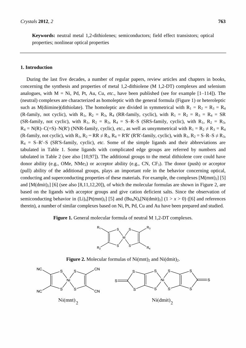
conducting and superconducting properties of these materials. For example, the complexes [M(mnt)2] [5]
and [M(dmit)2] [6] (see also [8,11,12,20]), of which the molecular formulas are shown in Figure 2, are
based on the ligands with acceptor groups and give cation deficient salts. Since the observation of
semiconducting behavior in (Li)x[Pt(mnt)2] [5] and (Bu4N)x[Ni(dmit)2] (1 > x > 0) ([6] and references
therein), a number of similar complexes based on Ni, Pt, Pd, Cu and Au have been prepared and studied.
Figure 1. General molecular formula of neutral M 1,2-DT complexes.
Figure 2. Molecular formulas of Ni(mnt)2 and Ni(dmit)2.

Crystals 2012, 2 764
Table 1. Simple 1,2-dithiolene ligands and their abbreviations.
edt
eds
dpedt
dmedt
dmeds
temedt
tmedt
tmeds
Pri2pipdt
Me2pipdt
Me2timdt
tdmdt
mtdt, dtm
mtds
bmsds
mdt
mds msds
dddt ddds
dsdds
pdt, pddt,
ddtdt
pds, pdds
psdds
mdddt dmdddt dcdt
ddt
dmvdt
edo
dmio, dmid dtods dmios,dsods
dmit sdsit
dsidt dmis(e) sdsit dsis
prdt prds qdt
mnt dmprdt
dmprds
dcit
i-dmit tdqs, tds
dcbdt
tbdt
pydt
hfdt
etodddt edodddt
bdt
dipth
Table 2. Some 1,2-dithiolene ligands referred by numbers.
L1
L2a (X = Br)
L2b (X = tBu)
L3a (X = S, Y = NR)
L3b (X = NR, Y = NR')
L4 *
L5a
L5b
L5c
S
S
Se
Se
S
SPh
Ph S
S
Se
Se
S
S
S
S
S
SN
N
Pri
Pri
S
SN
N
Me
Me
S
SN
NS
Me
Me
S
SMeS
MeS Se
SeMeS
MeS
S
SS
S Se
SeS
S Se
SeSe
Se S
SS
SSe
SeS
S Se
SeSe
Se
S
SS
SSe
SeS
S Se
SeSe
Se S
SS
S S
SS
S S
SC10H21S
C10H21S S
SS
S
S
SS
S S
SO
O S
SS
SO
Se
SeS
SO
Se
SeSe
SeO
S
SS
SS
Se
SeS
SS
Se
SeSe
SeS
S
SS
SSe
Se
SeS
SSe
Se
SeSe
SeSe
S
SN
N Se
SeN
N S
SN
N
S
SNC
NC S
SS
N
CN
S
SSS
S

Crystals 2012, 2 765
Table 2. Cont.
L5e
L5f
L5g
L6a–L6d
(R = Long chain)
L7
L8a
L8b
L8d L9 **
L10 ***
L11a (R = H),
L11b (R = Bu)
L12a
L12a'
L13
L14
L15a (X = Et, X' = Pent),
L15b (X = X' = iPr)
L16 ****
L17 (R, R several groups)
L18
* L4a (X = Me), L4b (X = Br), L4c (X = F), L4d (X = CF3), L4e (X = NO2), L4f (X = Cl), L4g (X = CN), L4h (X = H),
L4i (X = OMe); ** L9a (X = H), L9b (X = Me), L9c (X = Et), L9d (X = F), L9e (X = CF3), L9f (X = tBu), L9g (X = C6H6),
L9h (X = COOH), L9i (X = COOMe), L9ji (X = OMe), L9k (X = OC4H9), L9l (X = OC8H17), L9m (X = OC12H25), L9n
(X = OC14H29), L9on (X = OC16H33), L9p (X = OC18H37); *** L10a (X =H, X' = NMe2), L10b (X = OMe, X' = OH),
L10c (X = Oethylexyl X' = OH), L10d (X = OC10H21 X' = OH), L10e (X = OC10H21 X' = OMe), L10f (X, X' = Several
groups); **** L16a (X = H), L16b (X = Me), L16c (X = C12H25).
On the other hand, the complexes [Ni(dddt)2] [5] and [Ni(edo)2] [14], of which the molecular
formulas are shown in Figure 3, are based on ligands with donor ability and give cationic salts, which
are conducting materials [13–15,21].
Figure 3. Molecular formulas of Ni(dddt)2 and Ni(edo)2.

Crystals 2012, 2 766
The M 1,2-DT complexes exhibit some similarities to the so called TTF compounds of the
general formula (Figure 4) and selenium analogues, in which the central metal atom (M) of M 1,2-DTs
is replaced by the C=C group (see for example [12,16,21,85]). Generally, the TTFs such as ET (Figure 5),
exhibit weak semiconducting behaviour with energy gap of 2–3 eV, while M 1,2-DTs are better
semiconductors with HOMO/LUMO energy gap smaller than 1.5 eV. Some cationic salts of TTFs
exhibit similar behavior to that of M 1,2-DT cationic salts. For example [Ni(dddt)2]2X are isostructural
and exhibit metallic behavior as (ET)2X.
Figure 4. General molecular formula of TTF compounds.
Figure 5. Molecular formula of ET.
In recent years, a number of symmetrical M 1,2-DT complexes based on extended TTF-dithiolato
ligands, such as [Ni(dt)2] [22,23] and some unsymmetrical such as [Ni(dt)(dmit)] [48,49] (Figure 6)
and selenium analogues have been prepared and studied. A number of extended TTF-dithiolate ligands
are tabulated in Table 3. Dithiolene ligands could be coordinated as 1,2-enedithiolate dianions (as in
Tables 1–3), neutral dithioketones or mixed valence thioketones—radical thiolate monoanions—and
have been regarded both as innocent and non-innocent ligands [6–10,49,68]. These single component
(neutral) complexes exhibit semiconducting or metallic behaviour. Review articles, concerning neutral
complexes with N coordinated groups [97] or with ligands of Table 2 [102] and articles concerning
unsymmetrical complexes (of the type push-pull) [95], have been reported recently.
Figure 6. Molecular formulas of Ni(dt)2 and Ni(dt)(dmit).
Table 3. Extended TTF 1,2-dithiolene ligands and their abbreviations.
dt
dmdt
tmdt
dpdt
chdt
hfdt

Crystals 2012, 2 767
Table 3. Cont.
dmdtdt
Cn-tdt
mtdt
etdt
ptdt
dmetdt
eodt
dmstfdt
tmstfdt
a-tdt
dtdt
ds
dhdt ddmit ddmio
This paper is an overview of the published work concerning the preparation, properties and possible
applications of semiconducting neutral (single component) complexes based on Ni, Pt, Pd, Cu, Au and
on some ligands of Tables 1–3. Mainly, the work published since 2005 is considered [1–114]. The
results, obtained from unsymmetrical complexes in comparison to the corresponding symmetrical ones
in the solid state, are mainly discussed. They are compared to those obtained from the corresponding
TTFs and similar single component materials. More information concerning the ligands of Table 1 can
be found in [6–16,20,21,24,26–28,30,31,34,36,48–50,53,61–64,72,77,79,88,89,92,94,100–104]. More
information concerning the ligands of Table 2 can be found in the corresponding references for
L1 [34], L2 [34,98], L3 [33,95,102], L4 [56,73,102], L5 [97], L6 [61], L7 [75], L8 [58,60],
L9 [56,60,79,84,101,110,111], L10 [38,62,65,79,101,102,110], L11 [109,113], L12 [93,102], L13 [114],
L15 [33,102,114], L16 [57,102], L17 [102], and L18 [93,102]. More information concerning the
ligands of Table 3 can be found in the references [22,23,30,45,46,48,49,90]. Some related papers are
given in references [115–139]. They concern properties of TTFs [117,130–133], structural [115,123],
and electronic [118–121] properties of solids, electrochemical aspects [122], saturable absorbers [121]
and field effect transistors [116,124–129,134–138].
2. Experimental Methods/Techniques
2.1. Preparations
The first metal 1,2-dithiolene, the neutral bis[1,2-diphenyl-1,2-ethylenedithiolato (2−)-kS1,kS2]
nickel, abbreviated as [Ni(dpedt)2], was reported in 1962, derived from the reaction of diphenylacetylene

Crystals 2012, 2 768
with nickel sulfide [1]. Since then this compound and the Pt and Pd analogues have been prepared by
reaction of benzoin with P4S10, followed by addition of NiCl2, K2PtCl4, and K2PdCl4, respectively [2].
Today, a number of alternate methods are known, some of which are outlined here. The choice of
method depends, amongst other things, on the availability of the starting materials. Usually, as in the
case of the preparation of TTFs [9,12,16], 1,3-dithiole-2-ketones have been used as starting
materials [12,16,70,73–75,97,113] and the required neutral M 1,2-DTs were obtained from them,
according to a three-step procedure of Scheme 1.
Scheme 1. Procedure for synthesis of M 1,2-DTs from 2-ketones.
It should be noted that the choice of the oxidizing reagent (iii) or the electrooxidation conditions to
obtain the neutral compounds is based on redox potentials of the corresponding anionic complexes
(see below section 5).
With this method, the neutral complexes [Au(dpedt)2] [79] and Cu(L11)2 [109] have been prepared,
recently. In most cases, the deprotection of the ligand precursor is made with MeONa in N2
atmosphere and the addition of NiCl2 at low temperature [22]. In some cases, e.g., when the ligand is
dmit, dmio and etdt, cation deficient (1 > x > 0) complexes are obtained, instead of neutral ones
(see [6,12]). Also, the anionic salts, precursors of neutral complexes, could be obtained from several
starting materials (e.g., CS2, CSe2, vinylene trithiocarbonate) through the dianionic complexes of Zn or
Hg (see [6,9,12,16,30,130,131] and references therein) as in the procedures of Scheme 2.
Scheme 2. Procedures for syntheses of M 1,2-DTs from several starting materials.

Crystals 2012, 2 769
These Zn (or Hg) based anionic complexes react with NiCl2, PtCl2(PhCN)2, etc. to give the
corresponding mono and/or dianionic complexes of Ni, Pt, etc. [9,12,16]. Also, using the compounds
of Figure 7 and selenium analogues, as starting materials, the preparation of (neutral) M 1,2-DTs is
possible (see [9,14,36,48–50,52,63,64]).
Figure 7. Molecular formulas of a variety of starting materials.
Some examples of reactions are given here, in Scheme 3 [9,16,52].
Scheme 3. Some examples of reactions, using staring materials of Figure 7.

Crystals 2012, 2 770
The old method, using 1,2-diketones (or benzoins) as starting materials, was applied for the
preparation of a number of neutral complexes. The first step of the reactions is the conversion of diones to
dithions and/or to the phosphorus thioesters with P4S10 or Lawesson’s reagent. The next step of the
reactions is the hydrolysis and then the formation of neutral complexes using metal carbonyl or other
reactive salts, e.g., NiCl2, PdCl2(PhCN)2. The following Scheme 4 gives an example of the preparation
of a series of complexes from the corresponding 1,2-diketones [44,60,65,68,89,98,101,110,111].
Scheme 4. Procedure forpreparation of M 1,2-DTs from 1,2-diketones.
The unsymmetrical neutral complexes could be prepared by a ligand exchange reaction, which is
affected by refluxing two different neutral complexes as in the (reversible) reaction of Scheme 5
(see [4,14]), or by refluxing a neutral and a dianionic or two equivalent monoanionic complexes,
followed by oxidation. The unsymmetrical is isolated from the mixture as a second fraction of liquid
column chromatography. This means that the retardation factor of the unsymmetrical is in between the
factors of the corresponding symmetrical as in the cases of unsymmetrical and symmetrical
TTFs [9,12,16]. The rate of reaction depends on the solvent, the temperature and the nature of R and R'.
A number of unsymmetrical complexes of Ni, such as [Ni(dddt)(edo)], [Ni(ddds)(edo)], [Ni(edo)(ddt)],
[Ni(edo)(pdt)], [Ni(edo)(dtm)], [Ni(edo)(dmit)] and [Ni(edo)(mnt)] [14] have been prepared by
this method.
Scheme 5. Example of a ligand exchange reaction.
A similar kind of reaction by double substitution of an anionic salt with a cationic at ca. 50 °C has
been applied to the preparation of unsymmetrical complexes, as in the following Scheme 6.
S
S S
S
M
R
R R
R
S
S S
S
M
R'
R' R'
R'
S
S S
S
M
R
R R'
R'
Crystals 2012, 2 771
Scheme 6. Reaction of an anionic and a cationic salt.
By this method a number of the so called push-pull complexes, such as [Ni(H2pipdt)(dmit)],
[Ni(Pr2pipdt)(dmit)] [Ni(H2timdt)(dmit)], [Ni(Pr2timdt)(dmit)] and similarly with mnt instead of dmit
have been prepared [80,95].
Sometimes, the unsymmetrical complexes prepared by this method were contaminated with the
cationic-anionic double salts such as [Pt(Me2pipdt)2][Pt(dtcr)2] [15,95,106].
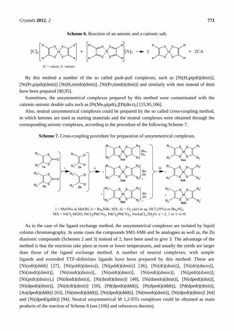
Also, neutral unsymmetrical complexes could be prepared by the so called cross-coupling method,
in which ketones are used as starting materials and the neutral complexes were obtained through the
corresponding anionic complexes, according to the procedure of the following Scheme 7.
Scheme 7. Cross-coupling procedure for preparation of unsymmetrical complexes.
As in the case of the ligand exchange method, the unsymmetrical complexes are isolated by liquid
column chromatography. In some cases the compounds SM1-SM6 and Se analogues as well as, the Zn
dianionic compounds (Schemes 2 and 3) instead of 2, have been used to give 3. The advantage of the
method is that the reactions take place at room or lower temperatures, and usually the yields are larger
than those of the ligand exchange method. A number of neutral complexes, with simple
ligands and extended TTF-dithiolato ligands have been prepared by this method: These are
[Ni(edt)(dddt] [27], [Ni(pddt)(dmio)], [Ni(pddt)(dmit)] [36], [Ni(dt)(dmit)], [Ni(dt)(dmio)],
[Ni(tmdt)(dmit)], [Ni(tmdt)(dmio)], [Ni(etdt)(dmit)], [Ni(etdt)(dmio)], [Ni(ptdt)(dmit)],
[Ni(ptdt)(dmio),] [Ni(dmdt)(dmit)], [Ni(dmdt)(dmio)] [48], [Ni(dmeds)(dmit)], [Ni(dpedt)(dsit)],
[Ni(dpedt)(dmit)], [Ni(dcdt)(dmit)] [50], [Pd(dpedt)(dddt)], [Pt(dpedt)(dddt)], [Pd(dpedt)(dmit)],
[Au(dpedt)(dddt)] [63], [Ni(tmedt)(dddt)], [Ni(dpedt)(dddt)], [Ni(tmedt)(dmit)], [Ni(dpedt)(dmio)] [64]
and [Ni(dpedt)pddt)] [94]. Neutral unsymmetrical M 1,2-DTs complexes could be obtained as main
products of the reaction of Scheme 8 (see [106] and references therein).

Crystals 2012, 2 772
Scheme 8. Some alternative procedures for the preparation of unsymmetrical complexes.
Generally, the cross-coupling method of Scheme 7 gave the unsymmetrical complexes in moderate
or low yield. However, a slight modification of the method, in which the deprotection of ligands takes
place with NaBH4, gave the unsymmetrical complexes obtained in better yield, according to the
procedure of Scheme 9 ([12,16,77,101].
Scheme 9. A modified procedure of cross coupling method.
In these preparations, the starting materials of the types SM1-SM6 could be used instead of 2a'–2c'
or 3a'–3c'. The complexes [Ni(dpedt)(dmit)], [Ni(dpedt)(dddt)] and [Ni(dpedt)(dt)] were prepared
by this method ([9,48,49] and work in progress). Generally speaking, from a number N = 100 ligands
of Tables 1–3, one can expect N(N + 1)/2 binary combinations, namely 5050 symmetrical and
unsymmetrical complexes for each metal, by applying several methods of preparation.
2.2. Growth and Morphology of Crystals
Single crystals suitable for X-ray structure solutions and electrical measurements have been
obtained from solutions in organic solvents. It has been found that the vapor diffusion method, using

Crystals 2012, 2 773
CS2 as solvent, and the dilute diffusion method [77,115] using hexane and CS2 as solvents give good
crystals of symmetrical and unsymmetrical M 1,2-DTs [36,50,63,64,79,84]. Also, crystals of neutral
complexes with an extended TTF-dithiolato ligand have been obtained by electroxidation of the
corresponding monoanionic or/and the dianionic complexes. (see [22,23,43,45,46]).
The crystals have a thin needle or thin platelet morphology. From a large number of crystals, only a
few of them have been suitable for X-ray structure solution and/or conductivity measurements.
2.3. Instrumentation and Background
The optical absorption (OA), crystal structure (CS), electrical (EL), and electrochemical (ELC)
data, described here, were obtained from measurements performed with commercial instruments, the
accuracy of which was considered good enough. Consequently, the results obtained by several groups
could be compared. The reported conductivity values have been obtained from measurements with the
two and/or four-terminal method.
The electrical parameters (e.g., the mobility) under conditions of field-effect transistor (FET)
were obtained from two-terminal measurements using the devices of Figure 8. Each of them consists
of a gate (G) electrode (e.g., n+-Si), a thin dielectric layer (e.g., SiO2, parylene), an organic
semiconductor (SM) layer (e.g., TTF, M 1,2-DT), a source (S) electrode and a drain (D) electrode
(e.g., Al, Ag, TTF·TCNQ, Au) on a substrate. Figure 8 shows two types of electrical connections:
with bottom-gate, bottom-contact configuration, suitable for polycrystalline deposits (Figure 8a) and
with a top-gate, top-contact configuration suitable for single crystals (Figure 8b).
Figure 8. Electrical connections and circuits for measurements under conditions of
field-effect transistor (FET): (a) The bottom-gate, bottom-contact configuration
(suitable e.g., for polycrystalline semiconducting films) and (b) the top-gate, top-contact
configuration (suitable e.g., for single crystal semiconductors) [124,128,129,136].

Crystals 2012, 2 774
The system looks like a gate/insulator/channel capacitor, where the channel is the 2-dimensional
layer of semiconductor between the S and D electrodes and insulator. When the gate is biased, a
current flowing between the S and D electrodes is measured as a function of length (L) and the
width (W) of the channel and other parameters concerning the system. The data were used for
characterization the system as electron current (n-type system) or hole current (p-type system) and
ambipolar (n-type and p-type).
The NLO response of the complexes has been obtained from measurements on homemade
apparatus using the Z-scan technique, which allows simultaneous determination of the sign and the
magnitudes as both the real (i.e., Reχ(3)
) and the imaginary (i.e., Imχ(3)
) parts of the third-order
nonlinear susceptibility χ(3)
of the material in one single measurement with lasers operating in a
wavelength of the visible (e.g., 532 nm) or near-IR (e.g., 1064 nm) region [35,48,99,100,111].
The magnitude of the molecular first hyperpolarizabilities of several unsymmetrical complexes was
determined from electric-field induced second harmonic (EFISH) generation experiments usually at
1.9 µm [80,95,106].
3. Structural Properties
In the most neutral M 1,2-DTs, the ligand forms a strictly square-planar arrangement, with all
S–M–S bond angles very close to 90°, but with variation in the value of intermolecular S–S contacts.
The neutral complexes may exist as planar monomers or form dimers with either metal-metal bonds or
metal-sulfur (selenium) bonds. Most of M 1,2-DTs were found to be crystallized in centrosymmetric
space group and, up to now, only three complexes have been found to be crystallized in non
centrosymmetric space group (see [7,10,15,17,20,63,64,69,94,97]). The data from selected M 1,2-DTs
are described here, starting from crystals with weak intermolecular interactions.
The symmetrical complex α-[Ni(dpedt)2], for example is crystallized in the centrosymmetric space
group P21/n, where Ni–S = 2.10, C–S = 1.71, C–C = 1.37 Å, S–Ni–S = 89.8, Ni–S–C = 107.3,
S–C–C = 118° [3,79]. The symmetrical complex [Au(dpedt)2] is crystallized in the tricliric space group
P1 and is isostructural with β-[Ni(dpedt)2], but not isostructural with α-[Ni(dpedt)2], [Pt(dpedt)2] and
[Pd(dpedt)2] [2,3,7,9]. Figure 9 shows the packing diagram of [Au(dpedt)2] [79]. In the molecules the
Au–S, C–S and the olefinic C–C bond lengths are ca. 2.29, 1.73, 1.37 Å, respectively. The bond
lengths M–S for the corresponding complexes of several metals (M) increase in the order
Au–S > Pd–S > Pt–S > Ni–S. In the cell of [Au(dpedt)2] the molecules are stacked along the b-axis.
Both interstacking and intrastacking S–S intermolecular distances are ca. 4.5 Å, i.e., much larger than
the sum of van der Waal’s radii (3.7 Å), while in (Bu4N)[M(dmit)2] these distances are 3.59–3.72 Å
(see [20] and references therein). This means that the complex has an almost 3D structure, with weak
S–S interactions. The long axis of the needle shaped crystals is almost parallel to the a-axis. In the
samples they have not been found in other habits. Some complexes of the type [Ni(L9)2] [56],
[Ni(L6)2] [61], and similar compounds of Au with ligands containing long chain groups [89,110] are
isostructural with [Au(dpedt)2] [79]. In [Au(bdt)2], isostructural with α-[Ni(dpedt)2], the S–S contacts
are 3.60–3.66 Å [29].

Crystals 2012, 2 775
Figure 9. Packing diagram of a crystal of [Au(dpedt)2]. Reproduced from [79] with
permission from Elsevier, and photograph of a crystal.
In the structure of symmetrical [Ni(dddt)2] [13,14], as in [Ni(dmit)2] [69], two molecules (A, B) of
the complex form independent uniform stacks along the b-axis. As in the crystal of neutral ET
(i.e., BEDT-TTF), there exists a dimer structure. Within the stacks of [Ni(dddt)2] the Ni–Ni is 4.67 Å.
There is no short intermolecular S–S contact (<3.70 Å) within the stack, and between molecules of
adjacent stacks (see [13,14] and references therein). In the structure of the symmetrical [Ni(edo)2]
(Figure 10) the molecules are planar, as in the case of [Ni(dddt)2], while in the corresponding TTFs
(i.e., BO and ET) are non-planar. The unit cell of [Ni(edo)2] contains two molecules, each of which is
repeated uniformly along the c-axis. The Ni–S bond lengths in [Ni(edo)2] are slightly larger than that
in [Ni(dddt)2] (2.12 Å).
Figure 10. Crystal structure of [Ni(edo)2]. Reproduced from [14] with permission of the
Royal Society of Chemistry.

Crystals 2012, 2 776
The neutral [Ni(dmit)2], studied years ago (see [20,69] and references therein), which is crystallized
in plate-like crystals of monoclinic space group P21/a, show that the molecules stack along the [010]
direction, making an angle with the normal to the molecule main plane of 48°. Within the stack, the
Ni–Ni spacing is 5.302 Å and the plane to plane distance 3.562 Å. In contrast to that observed in the
structure of (Bu4N)[Ni(dmit)2], (see [20,69] and references therein), in the structure of [Ni(dmit)2]
there are short S–S contacts between adjacent stacks involving the thioacetone sulfur atom
(ca. 3.58 Å) [69]. The complex [Ni(etoddt)2] (Figure 11) [100] crystallizes in the triclinic space group
Pl, and as in the case of [Au(dpedt)2] [79] there are no S–S contacts smaller than the sum of the van
der Waals radii.
Figure 11. Schematic presentation of the structure of [Ni(etoddt)2].
The unsymmetrical complexes [Ni(pddt)(dmio)], [Ni(tmedt)(dddt)], and [Ni(tmedt)(dmit)] are
isostructural and crystallized in the monoclinic space group P21/c [36,64]. Figure 12 shows a
perspective view of the [Ni(pddt)(dmio)] structure and a photography of the crystal. In a layer almost
parallel to the ab-plane there are S–S intermolecular contacts of 3.49 and 3.66 Å. In the other
directions the distances are larger. In [Ni(tmedt)(dddt)] and [Ni(tmedt)(dmit)] these contacts are 3.59 and
3.70–3.73 Å, respectively. The intermolecular contacts form a quasi-two-dimensional (q-2D) network.
It was found that the largest surface of the crystal is parallel to the crystallographic ab-plane.
Figure 12. Perspective view of the [Ni(pddt)(dmio)], reproduced from [36] with permission
of the Verlag der Zeitschrift für Naturforschung, and photograph of crystal [77].

Crystals 2012, 2 777
The complex [Ni(dmeds)(dmit)] crystallizes in the triclinic space group P1 13 shows that
the partial labeled plot of complex showing the intermolecular contacts [50]. The structure consists of
centrosymmetric dimers [7] with the inversion center sitting on the center of the Ni2Se2 core. The
closest Ni–S and Ni–Se bond lengths in the coordination sphere are ca. 2.2 and 2.3 Å respectively,
while the longer Ni–Se bond (2.56 Å) is responsible for the formation of the dimers. The closest
intramolecular Ni–Ni distance is ca. 3.06 Å. It was found that the largest surface of the rectangular
crystals is almost parallel to the crystallographic ab-plane. There are S–S and S–Se intermolecular
contacts of 3.594 and 3.560 Å, respectively, slightly smaller than the sums of van der Waals radii
(3.70 and 3.82 Å, respectively), which give rise to the formation of layers almost parallel to the ab-plane.
In other directions the distances are larger. This indicates a quasi two dimensional behavior of the material.
Figure 13. Partial labeled plot of [Ni(dmeds)(dmit)], reproduced from [50] with permission
of the Verlag der Zeitschrift für Naturforschung, and photograph of crystal [77].
The unsymmetrical complexes [Pd(dpedt)(dddt)], [Ni(dpedt)(dddt)] and [Ni(dpedt)(pddt)] are
isostructural and are crystallized in the orthorhobic non-centrosymmetric space group Pbc21 [63,64,94].
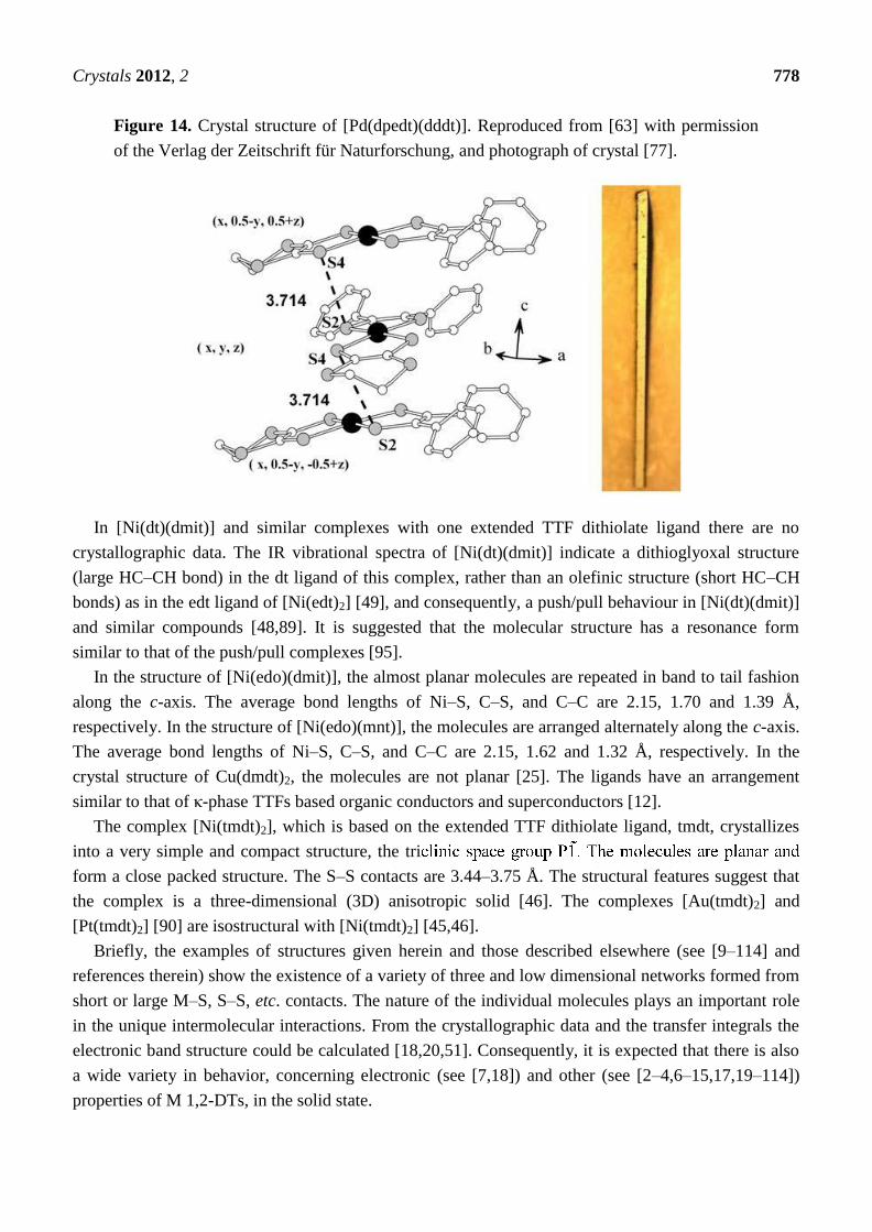
Figure 14 shows the stacking of [Pd(dpedt)(dddt)] molecules in a column along the c-axis. However,
there is no pseudocentro-symmetrical arrangement of molecules [20]. It was found that the needle axis
of the crystal is the c-axis. The shortest S–S distance in [Pd(dpedt)(dddt)] is 3.714 Å. The
intermolecular contacts form a q-1D network. In [Ni(dpedt)(dddt)] [64] and [Ni(dpedt)(pddt)] [94]
these distances are 3.764 and 3.738 Å, respectively, which are a little larger than the sums of van der
Waals radii (3.70 Å).
In some cases of unsymmetrical M 1,2-DTs, where one of the ligands has a push character
(dithione) and the other a pull character (dithiolate), the C–S and C–C distances in the two ligands are
different [31,80,95]. For example, in [Ni(Pr2timdt)(dmit)], the C–S and C–C distances for the ligand
Pr2timdt are 1.69 and 1.38 Å, while for the ligand dmit the distances are 1.74 and 1.29 Å, respectively.
In [Ni(tmedt)(dddt)] the push/pull character is weak and the corresponding values for tmedt are 1.68 and
1.37 Å, while for dddt are 1.71 and 1.38 Å [64,95]. Similar results as in [Ni(tmedt)(dddt)] have been
obtained from non centrosymmetric complexes [Pd(dpedt)(dddt)] [63], [Ni(dpedt)(dddt)] [64] and
[Ni(dpedt)(pddt)] [94].
Crystals 2012, 2 778
Figure 14. Crystal structure of [Pd(dpedt)(dddt)]. Reproduced from [63] with permission
of the Verlag der Zeitschrift für Naturforschung, and photograph of crystal [77].
In [Ni(dt)(dmit)] and similar complexes with one extended TTF dithiolate ligand there are no
crystallographic data. The IR vibrational spectra of [Ni(dt)(dmit)] indicate a dithioglyoxal structure
(large HC–CH bond) in the dt ligand of this complex, rather than an olefinic structure (short HC–CH
bonds) as in the edt ligand of [Ni(edt)2] [49], and consequently, a push/pull behaviour in [Ni(dt)(dmit)]
and similar compounds [48,89]. It is suggested that the molecular structure has a resonance form
similar to that of the push/pull complexes [95].
In the structure of [Ni(edo)(dmit)], the almost planar molecules are repeated in band to tail fashion
along the c-axis. The average bond lengths of Ni–S, C–S, and C–C are 2.15, 1.70 and 1.39 Å,
respectively. In the structure of [Ni(edo)(mnt)], the molecules are arranged alternately along the c-axis.
The average bond lengths of Ni–S, C–S, and C–C are 2.15, 1.62 and 1.32 Å, respectively. In the
crystal structure of Cu(dmdt)2, the molecules are not planar [25]. The ligands have an arrangement
similar to that of κ-phase TTFs based organic conductors and superconductors [12].
The complex [Ni(tmdt)2], which is based on the extended TTF dithiolate ligand, tmdt, crystallizes
into a very simple and compact structure, the tri
form a close packed structure. The S–S contacts are 3.44–3.75 Å. The structural features suggest that
the complex is a three-dimensional (3D) anisotropic solid [46]. The complexes [Au(tmdt)2] and
[Pt(tmdt)2] [90] are isostructural with [Ni(tmdt)2] [45,46].
Briefly, the examples of structures given herein and those described elsewhere (see [9–114] and
references therein) show the existence of a variety of three and low dimensional networks formed from
short or large M–S, S–S, etc. contacts. The nature of the individual molecules plays an important role
in the unique intermolecular interactions. From the crystallographic data and the transfer integrals the
electronic band structure could be calculated [18,20,51]. Consequently, it is expected that there is also
a wide variety in behavior, concerning electronic (see [7,18]) and other (see [2–4,6–15,17,19–114])
properties of M 1,2-DTs, in the solid state.

Crystals 2012, 2 779
4. Optical Properties
The optical properties of M 1,2-DTs in the form of single crystals, polycrystalline pellets, thin film
(or deposits), suspensions, composites and solutions have been reported in a number of papers. It was
observed, years ago, that the optical absorption (OA) spectra of solutions of monoanionic M
1,2-DTs (M = Ni, Pd, Pt), which are paramagnetic compounds, exhibit strong bands, which span the
range 700 to ca 1900 nm, depending on the nature of the metal, the ligand and the solvent (see for
examples [10,18,34,63,70]). The bands have been interpretated as the HOMO-LUMO transitions or as
ligand-to-ligand (LL) charge transfer (CT) transitions [34,95]. These bands and the bands of the
isoelectronic neutral Au 1,2-DTs have an unsymmetrical shape. After a Gaussian decovolution it has
been found that the bands are dominated by two transitions: one intense at low frequency is assigned to
1b1u→2b2g (x-polarized) and one medium to 1a1u→2b2g (y-polarized), as well as some weaker
ones [18,34]. The experimental values of transitions, i.e., the band position and intensity of OA bands,
have been found to be in reasonable agreement with the theoretically calculated ones [18,34]. The
splitting of the low frequency band is more discreet in the OA (and reflectance) spectra of the
complexes in the solid state (see for example [29] and refs. [9–11] cited therein).
Figure 15 shows the polarized reflectance spectra of (Bu4N)[Ni(dmit)2] with the wavevector of the
light parallel (R║) and perpendicular (R┴) to the needle axis of the crystal, as well as the OA spectra of
the material in CS2 solution and a suspension in CCl4. The reflectance spectra show anisotropic
behavior due to the low dimensional structure of the material [20,120]. In parallel polarization the band
is split into two sub-bands at 1100 and 1350 nm. The reflectance spectrum of a polycrystalline pellet
shows the same bands, while the spectra of a suspension of the material in CCl4 and that of the solution
in CS2 show narrow bands at ca. 1204 nm, with an unsymmetrical shape.
Figure 15. Polarized reflectance spectra of (Bu4N)[Ni(dmit)2], optical absorption (OA)
spectrum of a suspension of material in CCl4 (solid line) and of solution in CS2
(dashed line) [77].

Crystals 2012, 2 780
Different results have been obtained from cation deficient complexes. The reflectance spectra of
polycrystalline pellets of (Bu4N)x[Ni(dmit)2] and (Bu4N)x[Pt(dmit)2], obtained after oxidation of
monoanionic salts with iodine or bromine [6,12,47], are shown in Figure 16. In these cation-deficient
complexes (which behave as mixed-valence complexes) with x = 0.25 and x = 0.2, respectively, the
low frequency band-position, -intensity, and -shape depend on the x-value. When x→0, the (neutral)
complex exhibits a narrow band, blue shifted from that of monoanionic (x = 1), while for intermediate
values of x, the complex exhibits a new band at lower frequencies. The reflectance spectra of Figure 16
seem to be the superposition of those of a mixture of cation-deficient and neutral complexes.
Strong OA bands of cation deficient complexes (Bu4N)0.06[Au(eddt)2], (Bu4N)0.4[Pt(eddt)2] and
(Bu4N)x[Au(dmit)2] occur at ca. 860 nm [40], close to that of (Bu4N)0.2[Pt(dmit)2].
Figure 16. Reflectance spectra of polycrystalline pellets of (Bu4N)x[Ni(dmit)2] (a);
(Bu4N)x[Pt(dmit)2] (b). Reproduced from [54] with permission from Elsevier.
The OA spectra of neutral complexes exhibit strong bands, the position of which depends strongly
on the nature of the metal, the ligand the solvent, etc. The OA band positions (and intensities) of
unsymmetrical complexes (AB) in solutions occur in between those of the corresponding symmetrical
complexes (AA, BB). The characteristic OA wavelength (maximum or onset) is given by the equation:
λ(AB) = [λ(AA) + λ(BB)]/2 (1)
Figure 17 shows the experimentally observed spectra of [Ni(edt)2], [Ni(edt)(dddt)] and [Ni(dddt)2]
solutions in MeOH [27]. The observed OA band of the unsymmetrical [Ni(edt)(dddt)] occurs at
864 nm while, the calculated from those of symmetrical and Equation 1 was found at 867 nm.
The OA band position of neutral [Ni(dmit)2] in solution has been calculated from the positions of
the corresponding bands of some symmetrical Ni(L)2 and unsymmetrical [Ni(L)(dmit)] complexes
using Equation 1. It has been found to be ca. 1070 nm in CS2 and 1043 nm in CH3CN. The calculated
value for [Ni(dmio)2] is 932 nm in CS2. The OA spectra of some Au-based complexes and the OA
band position of Pd-based complexes in CS2 are shown in Figure 18. It can be seen that the
Au-materials exhibit wide transparent spectral regions, i.e., from ca. 500 nm to ca. 1500 nm. It was
found that the spectra of [Au(tmedt)(dddt)] and [Au(tmedt)2] in CS2 exhibit OA bands at ca. 1732
and 1500 nm, respectively. Generally, the OA bands of neutral Au 1,2-DTs occur at lower
frequencies, even, than those of monoanionic salts of Ni, Pd and Pt, which are isoelectronic

Crystals 2012, 2 781
(see Figures 17 and 18 for examples) [63,70]. The OA and reflectance bands of single crystals of
[Au(bdt)2] occur close to 2000 nm [29].
Figure 17. UV-vis/near IR absorption spectra of [Ni(dddt)2] (a); [Ni(edt)2] (b) and
[Ni(dddt)(edt)] (c) in MeOH. Reproduced from [27] by permission of the Verlag der
Zeitschrift für Naturforschung.
Figure 18. OA spectra of [Au(dpedt)2] (a), [Au(dpedt)(dddt)] (b) and [Au(dddt)2] (c):
arrows indicate the OA band positions of [Pd(dpedt)2] (d) [Pd(dpedt)(dddt)] (e) and
[Pd(dddt)2] (f) in CS2 [63,70].
The OA spectra of unsymmetrical M 1,2-DTs with a push-pull behavior, such as
M(Bz2pipdt)(mnt) [95,106], exhibit broad bands at ca. 751 (660sh), 651 (560sh) and 685 nm in DMF
for M = Ni, Pd, and Pt, respectively, with low to medium molar absorption coefficient and negative
solvatochromism [106]. The OA spectra occur between the spectra of the corresponding symmetrical
(if they exist), but do not obey Equation 1. Similar results have been obtained from
200 400 600 800 1000 1200
(a)
(c)
(b)
264303
240
298
420
375 551
1015
864
719
295
Absorb
ance (
a.u
.)
λ (nm)
500 1000 1500 2000
f
Absorb
ance (
a.u
.)
λ(nm)
1485
1670
1960
ab
c
905
980
1055
d
e

Crystals 2012, 2 782
[Pd(Me2Pipdt)(dmit)] [88] solutions in DMSO. In solution four peaks are present, and that at 737 nm
may be tentatively assigned to the HOMO-LUMO transition. This band shows negative
solvochromism and occurs at higher energy, when compared to the one in the corresponding Ni
compound (910 and 965 nm respectively, in CHCl3).
The position, intensity and shape of the bands in the solid state (single crystals, polycrystalline
pellets, thin deposits, etc.) depend on the structural feature of the complex. If the S–S contacts, for
example, are weak as in [Au(dpedt)2], the position of the OA band of a thin film occurs close to that of
the solutions, while, if the S–S contacts are strong as in the [Au(dddt)2] and [Au(bdt)2] [29], the OA
bands occur at lower frequencies.
As in the OA spectra of charge transfer (CT) and mixed valence (MV) compounds (see [117,120]),
the OA onsets or the Eg values of single component species (i), including small particles of M 1,2-DTs
could be obtained from the following Equation 2,
(Eg)i = ΔE − 2(t1)i − 2(t2)i (2)
where ΔE is the HOMO/LUMO gap, (t2)i and (t1)i the corresponding intermolecular transfer integrals.
These integrals could be obtained from band structure calculations based on crystallographic data.
Figure 19 shows the schematic presentation of bands and gap (Eg)i formation from a one dimensional
array of neutral molecules with HOMO/LUMO (H, L) gap of ΔE, where (t1)i and (t2)i are the
corresponding transfer integrals, for any species (i) concerning bulk (large t) and small particles (small
t). If the structure results from dimers, the energy gap is lower than the corresponding levels of dimers
[7,21,51]. Figure 20 shows the OA spectra of thin deposits of [Au(dpedt)2], [Au(dpedt)(dddt)] and
[Au(tmedt)2] obtained by rubbing the complexes on quartz plates. Because of the weak intermolecular
interactions in the solid state [63,79], the bands occur almost at the same positions as those of the
solutions, but are broader, and the fine structure is not clear. The same OA spectra have been obtained
from suspensions of the complex in CCl4 or toluene and from composites of the complex in a
polymethylmethacrylate matrix. However, the spectra of films, obtained by a spin-coating technique,
showed a fine structure [79], which could be attributed to several molecular transitions [34]. However,
in the cases of [Ni(etdt)2] [77], [Ni(dt)(dmit)] [49], [Ni(dmdt)(dmio)] [48] and [Ni(dmstfdt)(dmio)]
[48] the differences between the spectra of deposits and those of solutions are larger, because of the
stronger intermolecular interactions in the solid state. Figure 21 shows the OA spectra of [Ni(etdt)2]
thin deposits before (a) and after (b) rubbing as well as the spectrum of a solution in CS2 (c), for
comparison. Figure 22 shows the spectra of thin deposits of [Ni(dmdt)(dmio)] and
[Ni(dmstfdt)(dmio)]. It can be seen again that after extensive rubbing, the bands occur close to those of
the solutions, which indicates weak interactions [134].

Crystals 2012, 2 783
Figure 19. Schematic presentation of the bands and gap (Eg)i formed from the
HOMO/LUMO levels [7,12,21,51].
Figure 20. OA spectra of thin deposits of [Au(dpedt)2] (a) [Au(dpedt)(dddt)] (b) and
[Au(tmedt)2] (c) obtained by rubbing the materials on quartz plates [77,79].
Figure 21. OA spectra of thin deposits of [Ni(etdt)2] before (a) and after (b) rubbing on a
quartz plate and the OA band of a solution in CS2, for comparison (c) [77].
H
L
(E )g i
4(t )2 i
4(t )1 i
ΔΕ
400 600 800 1000 1200 1400 1600 1800 2000400 600 800 1000 1200 1400 1600 1800 2000
1500
1550
Ab
so
rba
nce
(a
.u.)
λ(nm)
1580
1441
1300
ab
c
500 1000 1500 2000 2500
Ab
so
rba
nce
(a
.u.)
(nm)
1410
1116
1020
(a)
(b)
(c)
1300nm
1550nm

Crystals 2012, 2 784
Figure 22. Panel I. OA spectra of thin deposits of [Ni(dmdt)(dmio)] before (a) and
after (b) rubbing on a quartz plate. The arrow indicates the OA band-position of a solution
in CS2. Panel II. same as panel 1, except for [Ni(dmstfdt)(dmio)]. Reproduced from [48]
by permission of the Verlag der Zeitschrift für Naturforschung.
The spectral behavior of [Ni(etdt)2], [Ni(dmdt)(dmio)], [Ni(dmstfdt)(dmio)], as well as that of
[Au(bdt)2] [29], reminds us of similar effects observed in the CT complexes such as KTCNQ [117] and
mixed valence complexes of the type X–M–X (where X = Cl, Br, I; M = Pt, Pd, Ni) [118].
The OA spectra of suspensions of neutral M 1,2-DTs occur close to those of the corresponding
solutions and obey Equation 1. As an example, the spectra of suspensions of [Ni(dmit)2], [Ni(dpedt)2]
and [Ni(dpedt)(dmit)] in CCl4 are given in Figure 23. The neutral [Ni(dmit)2], has been prepared in
single crystal form [69] and could be obtained in suspension form by injection of (Bu4N)x[Ni(dmit)2]
solution in CS2 into CCl4 containing I2, under vigorous stirring [6,12]. The calculated OA band
position of [Ni(dmit)2] from the corresponding band positions of [Ni(dpedt)2] and [Ni(dpedt)(dmit)] is
1047 nm, while the observed experimental value is 1017 nm ([50,54] and work in progress). This is
close to the calculated (above) for the spectrum of [Ni(dmit)2] in CH3CN-solution.
500 1000 1500 2000 2500
Ab
so
rba
nc
e (
a.u
.)
λ (nm)
1270
763
7881130
I
(a)
(b)
1550nm
1300 nm
500 1000 1500 2000 2500
Ab
so
rba
nc
e (
a.u
.)
λ (nm)
1312
1012
1550nm
(a)
(b)1300 nm
II

Crystals 2012, 2 785
Figure 23. OA spectra of suspensions of [Ni(dpedt)2] (a), [Ni(dpedt)(dmit)] (b) and
[Ni(dmit)2] (c) in CCl4 [77].
A large difference in the band positions and deviation from Equation 1 was observed in the spectra
of extended-TTF dithiolato ligands [45,46]. For example, the OA spectra of solutions of [Ni(dmdt)2]
and [Ni(dmdt)(dmit)] in CS2 show bands at 985 and 1037 nm, respectively. The OA band position of
[Ni(dmdt)2] calculated from Equation 1, occurs at 1089 nm. However, in the solid state, because of the
strong interactions in [Ni(dmdt)2] [32,45,46,134], the low frequency band occurs at ca. 4545 nm [46].
In other words, the OA-band positions and shapes of M 1,2-DTs, such as [Ni(etdt)2] and [Ni(ptdt)2],
with strong intermolecular interactions vary from sample to sample in the solid state (Figures 20–22
and Table 4). The reflectance spectrum of [Pd(Me2pipdt)(dmit)], except for the main peak at ca.
737 nm, shows an additional peak which could be attributed to an intermolecular transition involving
the dmit moieties interacting through short S–S intermolecular contacts [88].
Table 4. Optical absorption (OA) band position (nm) and OA onsets (eV), of a number of
selected M 1,2-DTs.
Complex Solvent Thin deposit Eopt
onset
CS2 CH2Cl2 (a) (b) (c)
[Ni(edo)2] 853 (1.34)
[Ni(dpedt)2] 875 (1.18)
[Ni(dmedt)2] 788 (1.36)
[Ni(ddt)2] 1033 (1.1)
[Ni(didt)2] 1007 (0.85)
[Ni(dmvdt)2] 1167 (1.0)
[Ni(dddt)2] 1033 1119 0.62 (1.0)
[Ni(tmdt)2] 1005 4545 0.25 (1.0)
[Ni(dmdt)2] 978 4545 0.25 (1.0)
[Ni(etdt)2] 1020 1410 1116 0.68 (1.25)
[Ni(ptdt)2] 1027 1000 2127 0.55 (1.0)

Crystals 2012, 2 786
Table 4. Cont.
[Pd(dpedt)2] 905 (1.18)
[Pd(dddt)2] 1055 (1.0)
[Pd(dt)2] 1289 (0.20)
[Pt(dpedt)2] 918 (1.37)
[Pt(dddt)2] 987 (1.15)
[Au(dpedt)2] 1485 1441 0.82 (0.82)
[Au(dddt)2] 1960 (0.55)
[Au(tmedt)2] 1500 1510 0.8 (0.08)
[Ni(edt)(dddt)] 894 870 954 893 1.02 (1.2)
[Ni(edt)(dmio)] 830 810 803 1 (1.15)
[Ni(edt)(dmit)] 906 875 (1.15)
[Ni(dmedt)(dmio)] 866 840 (0.95)
[Ni(dmedt)(dmit)] 933 901 870 1.02 (1.15)
[Ni(dpedt)(pddt)] 947 981 1.0 (1.08)
[Au(dpedt)(dddt)] 1670 1580 0.6 (0.63)
[Pt(dpedt)(dddt)] 906 1037 1.12 (1.2)
[Ni(dmeds)(dmit)] 950 914 1.03 (1.13)
[Ni(dpedt)(dsit)] 1005 (1.0)
[Ni(tmedt)(dmio)] 838 800
[Ni(tmedt)(dmit)] 945 1035 965 1120 0.79 (1.2)
[Ni(tmedt)(dddt)] 936 922 1020 1020 1058 0.89 (1.2)
[Ni(pddt)(dmio)] 978 921 935 0.8 (1.2)
[Ni(pddt)(dmit)] 1035 1003 950 933 0.78 (1.0)
[Ni(dddt)(dmio)] 978 (1.0)
[Ni(dddt)(dmit)] 1040 (1.12)
[Ni(mdddt)(dmit)] 1039
[Ni(dpedt)(dmio)] 906 884 897 0.99 (1.25)
[Ni(dpedt)(dmit)] 974 945 1007 940 1050 0.92 (1.1)
[Pd(dpedt)(dmit)] 1000 1022 0.88 (1.10)
[Pd(dmedt)(dmio)] 955 925 (1.15)
[Pd(dmedt)(dmit)] 1067 (1.07)
[Pd(dpedt)(dddt)] 980 1038 1.10 (1.12)
[Ni(dpedt)(dddt)] 955 933 1059 1058 1025 0.83 (1.06)
[Ni(dcdt)(dmit)] 1040 1004 999 1003 1025 0.74 (1.0)
[Ni(dt)(dmio)] 978 1245 1175 0.72 (1.05)
[Ni(dt)(dmit)] 1039 1245 1170 0.73 (1.03)
[Ni(dmdt)(dmio)] 977 1270 1130 0.70 (1.0)
[Ni(dmdt)(dmit)] 1037 1260 1170 0.72 (1.0)
[Ni(tmdt)(dmio)] 978 1250 1000 0.82 (1.2)
[Ni(tmdt)(dmit)] 1046 1360 0.72 (1.0)
Ni(dmstfdt)(dmio)] 988 1312 1012 0.83 (1.2)
[Ni(etdt)(dmio)] 982 1250 0.82 (1.06)
[Ni(etdt)(dmit)] 1035 1015 1300 1150 0.72 (1.0)
[Ni(pddt)(dmio)] 978 1238 1170 0.73 (1.13)
[Ni(pddt)(dmit)] 1041 1260 0.71 (1.0)
OA band position of thin deposits obtained by drop-casting (a); grinding rubbing (b) and spin-coating (c) techniques. Optical
onset values from the spectra of solutions in CS2 are given in parenthses.

Crystals 2012, 2 787
Table 4 gives the OA band positions and onsets in a number of selected M 1,2-DTs in solutions
(CS2, CH2Cl2) and in the solid state, which give information on the LUMO-HOMO gap and the energy
gap of material in the solid state (Eop
g = Eop
onset), respectively. One can see that this last parameter
varies from 0.62 to ca. 1 eV. The values of OA onsets were obtained from the OA spectra of thin
deposits. This means that the corresponding values from bulk materials (i.e., single crystals) should be
smaller. On the other hand, the values obtained from very thin deposits (and suspensions) will be
larger and close to those of solutions. In these cases the OA band positions of unsymmetrical and
corresponding symmetrical obey Equation 1. In the push-pull complexes the Eg-value is ca. 1.5 eV
(830 nm), while in complexes with extended-TTF dithiolato ligands this is small (<< 0.6 eV).
The spectra of Figures 18 and 20–22 show that the complexes have significant absorption maximum
near the telecommunication laser wavelengths (i.e., 1300 and 1550 nm). This is a requirement, which dyes
have to meet to be usable as optical filters, saturable absorbers, Q-switches and mode-lockers (see for
example [10,24,31,76,121]). Because of the wide transparent range, the band position, shape and intensity
as well as the stability in air, illumination of solutions of complexes with high power lasers exhibit some
other significant non-linear optical (NLO) properties [20,35,48,58,63,64,67,80,94,95,99,100,103,106,111].
For example, using solutions of symmetrical or unsymmetrical M 1,2-DTs the second hyperpolarizability γ
has been observed to be as large as 10−27
esu [35]. Also, from solutions of unsymmetrical complexes of
the type push-pull, a large value in the (negative) second polarizability (β) has been observed [106].
However, for similar observations concerning second harmonic generation from solid materials there is
no information. Although, there are known complexes with noncentrosymmetrical structures [63,64,94],
in these structures the molecules do not have a pseudo-centrosymmetric arrangement [20].
5. Chemical and Electrochemical Properties
The chemical and electrochemical reactivities, mainly of homoleptic M 1,2-DTs, reported before
2004, have been summarized in [8,19,24]. For results concerning new ligands and structures see [17–114].
Also, for a wide range of electrochemical aspects of molecular solids see [122]. Examples, concerning
chemical reactivity, are ligand exchange reactions as well as ligand addition and substitution reactions.
Methods of preparations of neutral and unsymmetrical complexes, based on these kinds of reactions,
have been already described in section 2. The selection of reactions as well as the selection of
oxidizing, or reducing agents for the preparation of stable (in air) complexes are related to the
electrochemical (redox properties) of the materials. The cyclic voltametry (CV) measurements of
M 1,2-DTs provide useful electrochemical parameters. These are the half wave redox potentials,
defined as E1/2(i) = [Eox(i) + Ered(i)]/2, where Eox(i) and Ered(i) are the oxidation and reduction
potentials of several redox couples (i = 2−/1−, 1−/0, etc.), respectively. These parameters play an
important role in the formation, stability and other properties of M 1,2-DTs and their salts. Figure 24
shows a schematic presentation of a voltammogram of a M 1,2-DT and that of a donor molecule, e.g.,
of a TTF compound, for comparison. One can see that there are some common features at their
positive potentials, which lead to the formation of cationic salts in both cases [16,21]. The couple
E1/2(0/x+) (0 < x ≤ 1) is rare [79,95]. Instead of which, an irreversible wave E(0/x+) is observed
However, in the negative potentials there are considerable differences: the couples concerning 1−/0
(or 2−/1−) states are absent or rare in the voltammograms of donor molecules [12,16]. These couples

Crystals 2012, 2 788
are observed in the voltammograms of acceptors, e.g., of TCNQ (0.17, −0.37 V vs. SCE), and
TCNQ(CN)2 (1.31, 0.51 V vs. SCE) [122–124].
Figure 24. Schematic presentation of a voltammogram of a M 1,2-DT (a) and a
voltammogram of a TTF derivative, for comparison (b) [16,79].
-10
-5
0
5
10
-3,0 -2,5 -2,0 -1,5 -1,0 -0,5 0,0 0,5 1,0 1,5 2,0
-1,6
-1,2
-0,8
-0,4
0,0
0,4
0,8
1,2
-0,786
0,026
0,981
-0,089-0,913
0,855
I (μ
A)
0/X+2-/1-
onsetE
rd = 0.1
I
(μA
) onsetE
ox = 0.8
(a)
E (V) vs Ag/AgCl
1-/0
1+/2+0/1+
(b)
1.145
1.225
onsetE
ox = 0.45
onsetE
rd = -2.2
0.624
0.515
1-/0
In the literature, it can be found that there are a wide variety of redox values obtained from
M 1,2-DTs under different conditions and electrochemical techniques. To help compare studies
employing different reference electrode-couples, the redox potential values are converted versus a
common reference electrode, the saturated calomel electrode (SCE), which is approximately equivalent
to the Ag/AgCl electrode, according to the following relationship [19]: Ag/AgCl (in satur.
KCl solution) = SCE (in satur. KCl solution) + 0.045 = Fc/Fc+ (in 0.2 M LiClO4/MeCN) + 0.352 =
Ag/Ag+ + 0.604 = NHE − 0.196 (V).
The conversion factors depend on the solvent and the supporting electrolyte [19,42,77]. Tables 5–8
give the E1/2(2−/1−), E1/2(1−/0) and E(0/x+) (in V versus Ag/AgCl) as well as other electrochemical
and OA data observed at room temperature from a number of selected M 1,2-DTs and selenium
analogues. The difference E(0/x+) − E1/2(1−/0) ≈ Eonsetox
− Eonsetrd
= ΔE is a measure of the electronic
energy gap of the materials in solutions or suspensions [45,46,63,64,77,79]. One can see that the
results from electrochemical measurements (of solutions, Egelc
) are in agreement with the optical
absorption Eonsetopt
of solutions in CS2, while there is a large deviation from the data in the solid state
(OAmax and Eonsetopt
of deposits or pellets), as well as from the electrical measurements (Egel)
(see below). This is a consequence of the variety of intermolecular interactions arising from the S–S
contacts, in the solid state. Namely, the difference is larger in cases of complexes with strong S–S
interactions (Table 8). From these data, the HOMO and LUMO energy levels could be calculated via
the following equations (see [47–50,63,64,79] and references therein).
EHOMO = −(4.4 + Eox
onset) (3)
ELUMO = −(4.4 + Erd
onset) (4)

Crystals 2012, 2 789
Table 5. Redox potentials (V) and (solid state) OAmax (eV) of complexes * [14,64,77].
Complex E1/2 (2−/1−) E1/2 (1−/0) E (0/x+) OAmax
[Ni(dmedt)2] −1.070 −0.229 1.079 1.28
[Ni(tmedt)2] −0.910 −0.140 1.050 1.24
[Ni(tmedt)(dddt)] −0.827 −0.099 0.964 1.21
[Ni(dpedt)2] −0.864 −0.063 1.012 1.38
[Ni(dddt)2] −0.744 −0.058 0.875 1.04
[Ni(dpedt)(dddt)] −0.794 −0.039 0.988
1.17 (−0.804) (−0.060) (0.943)
[Ni(dmedt)(dmit)] (−0.651) (+0.039) (1.207) 1.31
[Ni(tmedt)(dmit)] −0.571 +0.064 1.197 1.28
[Ni(dpedt)(dmit)] −0.559 +0.167 1.187
1.21 (−0.544) (+0.102) (1.173)
[Ni(dpedt)(dmio)] −0.532 +0.170 1.185 1.38
[Ni(dddt)(dmit)] (−0.488) (+0.210) (1.105) 1.02
[Ni(dmit)2] −0.232 +0.268 1.335 0.92
[Ni(dmio)2] −0.200 +0.297 1.358
[Ni(edo)2] −0.75 −0.26 0.71
[Ni(mnt)2] −0.10 −0.81
[Ni(Pr2pipdt)(dmit)] −1.165 −0.593 0.590
[Ni(Me2pipdt)(mnt] −0.963 −0.527 0.908
[Ni(Pr2tipdt)(mnt)] −0.307 0.354 1.160
* Observed vs. Ag/AgCl electrode. Calculated values from the equation E1/2(AB) = [E1/2(AA) + E1/2(BB)]/2
are given in parentheses (where AA and BB are the symmetrical and AB the corresponding unsymmetrical
complexes); 0 < x ≤ 1; E (0/x+) usually is irreversible wave; OAmax in solid state.
Table 6. Electrochemical * and (solid state) OA ** data of selected complexes [64,77].
Complex Eonsetrd
(V) Eonsetox
(V) Eonsetop
(eV) ELUMO (eV) EHOMO (eV)
[Ni(dmedt)2] −0.145 0.958 1.18 [1.10] −4.25 −5.36
[Ni(tmedt)2] −0.135 0.905 0.90 [1.03] −4.26 −5.30
[Ni(tmedt)(dddt)] −0.042 0.837 0.88 [0.88] −4.36 −5.24
[Ni(dpedt)2] 0.000 0.860 0.95 [0.86] −4.40 −5.26
[Ni(dddt)2] +0.052 0.770 0.76 [0.72] −4.45 −5.17
[Ni(dpedt)(dddt)] +0.100 0.833 0.82 [0.73] −4.50 −5.23
[Ni(dmedt)(dmit)] (+0.122) (1.024) 0.91 [0.90] (−4.52) (−5.42)
[Ni(tmedt)(dmit)] +0.142 0.997 0.95 [0.86] −4.54 −5.39
[Ni(dddt)(dmit)] (+0.221) (0.930) 0.80 [0.71] (−4.62) (−5.33)
[Ni(dpedt)(dmit)] +0.270 1.020 0.85 [0.75] −4.67 −5.42
[Ni(dpedt)(dmio)] +0.280 1.017 0.92 [0.74] −4.68 −5.42
[Ni(dmit)2] +0.390 1.090 1.0 [0.70] −4.79 −5.48
[Ni(dmio)2] +0.450 1.130 1.1 [0.68] −4.85 −5.53
* Observed vs. Ag/AgCl. Calculated values from equation Eonset(AB) = [Eonset(AA) + Eonset(BB)]/2 as well as
the corresponding ELUMO and EHOMO values are given in parentheses; ** Eonsetop
observed from thin deposits.
Calculated Eonsetop
values (=Egelc
) from electrochemical data (Eonsetox
− Eonsetrd
) 1 eV, considering x = 1, are
given in brackets.

Crystals 2012, 2 790
Table 7. Calculated ELUMO and EHOMO values and the corresponding electrochemical and
optical absorption data [63,79].
Complex E1/2(1−/0) Eonsetrd Eonset
ox Eonsetopt ELUMO * EHOMO *
(V) (V) (V) (eV) (eV) (eV)
[Ni(dpedt)(pddt)] +0.036 +0.155 +0.884 0.88 −4.55 −5.28 [−5.43]
[Ni(dpedt)(dddt)] −0.039 +0.100 +0.833 0.82 −4.51 −5.23 [−5.33]
[Pd(dpedt)(dddt)] +0.030 +0.161 +0.797 0.92 −4.56 −5.20 [−5.48]
[Pt(dpedt)(dddt)] +0.055 +0.070 +0.900 0.95 −4.47 −5.30 [−5.42]
[Ni(dpedt)(dmit)] +0.167 +0.270 +1.020 0.85 −4.67 −5.42 [−5.52]
[Pd(dpedt)(dmit)] +0.230 +0.250 +0.920 0.96 −4.65 −5.32 [−5.41]
[Au(dpedt)(dddt)] +0.300 +0.350 0.850 0.65 −4.75 −5.25 [−5.40]
[Au(dpedt)2] +0.315 +0.403 0.852 0.61 −4.83 −5.22 [−5.44]
* The ELUMO values were calculated from the reduction onset values (−ELUMO = 4.4 + Eonsetrd
). The EHOMO
values were calculated from the oxidation onset values (−EHOMO = 4.4 + Eonsetox
). Also, EHOMO values
calculated from electrochemical and OA data (EHOMO = ELUMO − Eonsetopt
) are given in brackets.
Table 8. Electrochemical, optical and electrical data for selected M 1,2–DTs [48–50,77].
Complex E1/2(1−/0) E(0/x+) Egelc OAmax Eonset
opt Egel
[Ni(dmdt)2] −0.14 0.74 0.88 4545 0.25 [1.0] 0
[Ni(tmdt)2] −0.12 0.80 0.92 4545 0.25 [1.0] 0
[Ni(dt)2] 0.01 0.070
[Pd(dt)2] 1289 0.2 [1.0]
[Ni(ptdt)2] −0.04 1.39 1.35 2127 0.55 [1.0] 0.060
[Ni(etdt)2] −0.05 1417 0.50 [1.1]
[Ni(dmdt)(dmio)] (0.08) 1270 0.60 [1.0]
[Ni(dmdt)(dmit)] 0.72 [1.0]
[Ni(dmstfdt)(dmio)] 1212 0.83 [1.2]
[Ni(dt)(dmit)] (0.14) 1245 0.73 [1.03]
[Ni(pddt)(dmio)] 0.80 [1.2] 0.26, 0.36
[Ni(dmeds)(dmit)] 1.03 [1.13] 0.38, 0.36
Electrochemical data: E1/2(1−/0), E(0/x+) and Egelc
E(0/x+) − E1/2(1−/0) (V, versus Ag/AgCl electrode);
OAmax position of a thick deposit (polycrystalline samples) (nm); Eonsetopt
of the OA band in solid state
(deposits or pellets) (eV); the corresponding onset from solutions in CS2 are given in brackets and the energy
gap from electrical measurements, Egel
(eV).
These are applied when the Eonsetox
and Eonsetrd
are given versus Ag/AgCl as reference electrode. If
one of the Eonset is observed by CV, this value and the difference Eonsetox
− Eonsetrd
≈ Eonsetop
obtained
from the OA spectra of solutions, suspensions or very thin films could be used for the calculation of
HOMO and LUMO energy values. However, HOMO energy values could be estimated from
ultraviolet photoelectron spectra and the LUMO energy values from the inverse photoelectron spectra,
in the solid state [125]. The electrochemical parameters of unsymmetrical M 1,2-DTs (AB) occur in
between those of the corresponding symmetrical (AA, BB) as in the case of the OA parameters. If the
couples are reversible, the redox values obey the following equation as in the case of TTFs [16].
E(AB) = [E(AA) + E(BB)]/2 (5)

Crystals 2012, 2 791
The calculated values of several unsymmetrical complexes are given in Tables 5–8 in comparison to
the observed ones. It can be seen that the values of LUMO and HOMO levels vary from ca. 4.25 to
4.85 and from ca. 5.17 to 5.68 eV, respectively. It has been demonstrated that these compounds are
stable in air (H2O + O2), because the LUMO value is larger than 4 eV (see [47] and references therein).
This finding is almost equivalent with the suggestion that the species (such as neutral M 1,2-DTs) with
E1/2 < 0.00 V (vs. SCE) are susceptible to air oxidation in solution (H2O + O2), while species with
E1/2 > 0.00 V are stable in air. A number of neutral M 1,2-DTs were prepared by oxidation of the
corresponding anionic complexes. In these reactions and others similarly involving oxidation, proper
selection of the oxidizing agent is crucial. However, the knowledge of the redox values of the species
could be a guide to the synthesis of new compounds [14,15,48–50,64,77]. For example, if the species
has E1/2 < 0.2 V the oxidation can be obtained with I2, otherwise, a stronger oxidant should be used [19].
Also, if a monoanionic M 1,2-DT has two reversible redox processes between the dianions and neutral
complexes at ca. −0.7 and 0 V (vs. Ag/AgCl) as in [Ni(dddt)2] further oxidation is associated with the
formation of partially oxidized compounds {M 1,2DT]x+
. If these values are −0.23 and 0.26 V, as in
[Ni(dmit)2], the oxidation gives cation deficient salts such as [Ni(dmit)2]x−
. In the cases of complexes
with extended TTF dithioleto ligands these values are ca. −0.4 and 0 V, respectively, the oxidation
gives neutral complexes. In other words, the knowledge of redox values is a guide for fabrication of
several stable (in air) electronic and optoelectronic devices (see below).
6. Electrical Properties
As in other cases of organic and inorganic materials, one may classify M 1,2-DTs as metals with
room temperature conductivity σΡΤ ≥ 102 Scm
−1, semiconductors with 10
2 ≥ σRΤ ≥ 10
−10 Scm
−1, and
insulators with σΡΤ ≤ 10−10
Scm−1
[20–27,51]. Monoanionic M 1,2-DTs are weak semiconductors or
insulators; cationic are metallic or semiconducting materials, while cation deficient and neutral could
be semiconducting or metallic. Some cation deficient complexes are superconducting materials [20–27].
From the neutral (i.e., single component) M 1,2-DTs, some symmetrical, usually with extended
TTF-dithiolato ligands, were found to be metallic without the need to form charge transfer salts ([22,26,35]
and references therein). It has been considered that, unlike conventional organic conductors (i.e., those
based on TTFs) consisting of π-conduction layers and insulating anionic layers, the single compound
molecular conductors (i.e., M 1,2-DTs) tend to have 3D stable metallic bands [43]. Here, the results
obtained mainly from neutral symmetrical and unsymmetrical complexes, based on some ligands of
Tables 1–3, with semiconducting behavior, as well as those obtained from some anionic complexes for
comparison are primarily discussed. The electrical characteristics of some neutral complexes are
tabulated in Table 9 with the corresponding structural and optical ones, for comparison. In the cases of
monoanionic complexes, such as (Bu4N)[Ni(dmit)2] and (Bu4N)[Ni(dddt)2], the conductivity at room
temperature has values 10−8
and 5 × 10⁻⁵
S/cm, respectively. However in cation deficient compounds
of the type (Bu4N)x[Ni(dmit)2] the room temperature conductivity varies from 10−3
to 10 S/cm as x
increases from 0.25 to 0.29 (see [20] and ref. 102 cited therein). Figure 25 shows the resistivity versus
the temperature and versus the inverse temperature for a polycrystalline pellet of (Bu4N)0.25[Ni(dmit)2]
(see [9] and ref. 20 cited therein, [54] and ref. 6 cited therein, [69] and ref. 26 cited therein).

Crystals 2012, 2 792
Table 9. Structural, optical and electrical characteristics of some neutral
M 1,2-DTs [15,23,29,36,43,45,46,57,77,90].
Complex Space
Group S–S (Å)
OAmax
(nm, CS2)
OAmax
(nm, Sol. St) σRΤ (Scm
−1) Ea(meV)
α-[Ni(dpedt)2] P21/n 875
β-[Ni(dpedt)2] Pī
875
[Ni(dddt)2] P21/a
<3.70 1033 >1119
[Ni(dmit)2] >> <3.70, 3.58 1030 1017 Sem. 3.5 × 10⁻³
[Ni(etoddt)2] Pī <3.70
[Ni(tmedt)(dddt)] P21/c 3.59 936 1030
[Ni(tmedt)(dmit)] >> 3.70–3.73 945 1037
[Ni(pddt)(dmio)] >> 3.49, 3.56 978 935 Sem. 2.5 × 10⁻⁵
, 1 × 10⁻⁹
130, 180
[Ni(dmeds)(dmit)] Pī 3.59 950 920 Sem. 1.5 × 10⁻⁵
, 2.5 × 10⁻⁸
190, 180
[Ni(dpedt)(dddt)] Pbc21 3.76 955 1059
[Ni(dpedt)(pddt)] >> 3.746 947 981
[Au(dpedt)2] Pī 4.5 1480 1480
[Au(dddt)2] P21/n 3.59–3.67 1960 Sem. 1 × 10⁻⁴
[Au(bdt)2] >> 3.60–3.66 2062 Sem. 0.11
[Ni(dmdt)2] Pī 978 4595 300–400 Met > 230 K
[Pd(dmdt)2] Sem. 150
[Ni(tmdt)2] Pī 3.44–3.75 1005 4595 300–400 Met > 0.6 K
[Co(dmdt)2] Sem. 0.05 85
[Co(tmdt)2] Sem. 1.5 24
[Cu(dmdt)2] <3.7 Sem. 3.0 40
[Cu(tmdt)2] Sem. 5.1 63
[Au(dmdt)2] Sem. 12 9
(300–50 K)
[Au(tmdt)2] Pī 3.43–3.64 Sem. 15 20
(300–50 K)
[ Ni(dt)2] Sem. 16 35
[Pd(dt)2] P21/m <3.7 1282 Sem. 0.3 94
[Co(dt)2] Met. 19
[Ni(etdt)2] Sem. 10−4
[Ni(eodt)2] 8 Met > 120K
[Ni(chdt)2] Sem. 2.0 38
[Ni(hfdt)2] Sem. 1.4 × 10⁻⁴
22
[Au(hfdt)2] Sem. 3.2 × 10⁻⁴
220
[Ni(ptdt)2] C2/m 3.37 2127 Sem. 7 30
[Pt(tmdt)2] 350 Met > 4 K
[Ni(tmstsdt)2] 100 Met > 100 K
[Ni(dtdt)2] 2.5–200
[Au(dtdt)2] 8
[Ni(a-tdt)2] 2.5–24
[Au(a-tdt)2] 5
[Au(ptdt)2] 3.26 2

Crystals 2012, 2 793
Figure 25. Resistivity versus the temperature (a,c,d,e,f) and versus the inverse temperature
(b) for polycrystalline pellets of (Bu4N)0.25[Ni(dmit)2] (a,b) [77], [Ni(chdt)2] (c),
[Ni(eodt)2] (d) and [Ni(tmdt)2] (e) as well as in a single crystal of [Ni(tmdt)2] (f). Panel c
and d was reproduced from [22] and panel e and f from [23] with permissions of the
American Chemical Society.
.
From the slopes of the plots the activation energy (Ea) and/or the energy gap (Eg), values could be
calculated via the Arrhenius equation where ρo is a temperature independent constant, k is the
Boltzman constant and Ea = Eg/2. For the cation deficient compound (Bu4N)0.25[Ni(dmit)2] the
activation energy at low temperatures was found, via this equation, to be 84 meV [77]. Cation deficient
complexes based on dmit with several cations, metals and compositions (x) were found to be
semiconductors, conductors and superconductors (see [20,69]). Some neutral M 1,2-DTs and TTFs
exhibit similar behavior (see [15,21,77]). Single crystals of the neutral [Ni(dmit)2] exhibit
semiconducting behavior with σRΤ = 3.5 × 10⁻³
S/cm [69]. Figure 25 shows ρ vs. T of polycrystalline
pellets of [Ni(chdt)2] and [Ni(eodt)2] [22] as well as, ρ vs. T of a polycrystalline pellet and a
single crystal of [Ni(tmdt)2] [23]. The change in behavior (from metallic to semiconducting) is due to
(6)

Crystals 2012, 2 794
the decreasing intermolecular contacts as was observed in the optical absorption spectra
(Figures 21 and 22). Figure 26 shows the plots of ρ vs. 1/T, obtained from a single crystal of
[Ni(pddt)(dmio)] [36] of which the crystal structure has already been discussed above. It was found
that the room temperature conductivity is σRΤ(||) = 2.5 × 10⁻⁵
Scm−1
and σRΤ (┴) = 1 × 10⁻⁹
Scm−1
.
This means that there is anisotropy of 2.5 × 10⁴. From Equation 6, one can find Ea(||) =0.13, and
Ea(┴) = 0.18 eV [35].
Figure 26. Plots of resistivity versus the inverse temperature for a single crystal of
Ni(pddt)(dmio) with current approximately parallel (||) and perpendicular (┴) to the ab-plane.
Reproduced from [36] by permission of the Verlag der Zeitschrift für Naturforschung.
Figure 27 shows the resistivity versus the inverse temperature for a single crystal of
[Ni(dmeds)(dmit)] with currents approximately parallel (a) and perpendicular (b) to the ab plane [50].
In this case σRT(||) = 1.5 × 10⁻⁵
Scm-1
, σRT() = 2.5 × 10⁻⁸
Scm−1
, σRT(||)/σRT(┴) = 6 × 10², Ea(||) = 0.19,
and Ea(┴) = 0.18 eV [50], for the current parallel (||) and perpendicular (┴) to the ab-plane. It has been
found that after a series of heating/cooling cycles the resistivity decreases [50].
Figure 27. Plots of resistivity versus the inverse temperature for a single crystal of
[Ni(dmeds)(dmit)] with current approximately parallel (||) and perpendicular (┴) to the
ab-plane, before (I) and after (II) applying a number of heating/cooling cycles. Reproduced
from [36] by permission of the Verlag der Zeitschrift für Naturforschung.

Crystals 2012, 2 795
Conductivity measurements on compressed pellets of [Ni(dmeds)(dmit)], [Ni(dmedt)(dmit)] and
[Ni(dpedt)(dsit)] gave σRT(pellet) = 1 × 10⁻⁶
, 1.2 × 10⁻⁷
, and 1 × 10⁻⁷
–5 × 10⁻⁶
Scm−1
, respectively.
The Eg(pellet) values were found to be 0.45, 0.50–0.80 and 0.46 eV, respectively. The σRT values of
[Ni(dpedt)(dmit)] and [Ni(dcdt)(dmit)] were found to be very small (<10−9
Scm−1
) [35,50,58].
Measurements on a single crystal of [Au(bdt)2] showed, σRT(||) = 0.11 Scm−1
and Ea(||) = 0.3 eV [29].
From structural, optical and electrical data from single crystals or polycrystalline samples, reported
above and/or summarized in Tables 4 and 9, it can be expected that the energy gap values of each
sample (or crystallographic directions) obey Equation 2. This means that, as the interactions increase,
the Eg decreases, the optical absorptions bands are red shifted and the material, because of Equation 6,
becomes more conducting (see also [32,134]). Calculations of t1 and t2 from crystallographic data are
needed for a comparison with the experimental data. The conductivity measurements on some
M 1,2-DTs after illumination with visible-near IR light exhibit a broad band close to that of the OA
band [24,59,62]. These materials can be used as photodetectors [24,59,62].
Recently, the results of electrical measurements on M 1,2-DTs under the conditions of field effect
transistor (FET) have been reported [37,39,47,56,57,65,93,113]. These results are discussed here and
compared with those obtained from donors (e.g., TTFs) or acceptors (e.g., TCNQ) [51,66,126].
Mainly, electrical circuits like those shown in Figure 8 suitable for measurements on thin deposits or
single crystals of M 1,2-DTs have been used. The observed currents are due to the semiconductor-insulator
interface which is a thin (2-dimensional) layer in the semiconductor size, the channel of the
semiconductor; the rest of the material is inert and does not contribute drastically to this kind of
current. As an example, the process of measurement on [Ni(dpedt)(dmit)] thin film is described [47].
Si wafers of (p-type) as a gate electrode, with 200 nm SiO2 layer at the gate electrode, gold source and
drain electrodes were defined in a two terminal bottom contact configuration (Figure 8a), with channel
width (W) of 10 mm and length (L) of 10 µm. A 10 nm titanium was used as an adhesion interlayer for
the gold on SiO2. The SiO2 was treated with the primar hexamethyldisilazane prior to semiconductor
deposition, in order to passivate its surface. Films of [Ni(dpedt)(dmit)] were then drop cast on top from
a solution in CH2Cl2. Under appropriate biasing conditions strong hole and electron accumulation has
been observed. In particular, for negative drain (VD) and gate (VG) voltages, accumulation of holes is
evident, while for positive VD and VG, electron accumulation has been observed. Figure 28a shows the
output current-voltage characteristics and Figure 28b shows the transfer characteristics at various drain
voltages on a channel of [Ni(dpedt)(dmit)] [47]. From the curves and the Equations 7 and 8, the hole and
electron field effect mobilities (µh, µe) have been calculated.
Where Ci is the capacitance per unit area of the insulator layer (given by Ci = εεο/d, with d the
thickness of the layer, ε is the dielectric constant of the insulator and εο the permittivity in vacuum).
From the calculations the maximum hole and electron mobilities have been found to be 1 × 10⁻⁴
and
3 × 10⁻⁴
cm2/Vs, respectively. The on-off current ratio was calculated from the data of the transfer
characteristics and Equation 9 assuming that the semiconductor film of thickness t has a uniform (bulk)
conductivity, σ, and uniform mobility, μ, the ratio is of the order 102–10
3.
For linear regime
(7)
For the saturated regime
(8)

Crystals 2012, 2 796
12
oni D
off
I μCV
I σt (9)
Figure 28. Output current-voltage characteristics (a) and transfer characteristics at various
drain voltages (b) obtained from an ambipolar channel based on [Ni(dpedt)(dmit)].
Reproduced with permission from [47] by permission of the American Institute of Physics.
Measurements on (NO)x[Ni(dmit)2] (1 > x ≥ 0) films showed that the behaviour is of n-type in any
x value [25]. When x = 1 (monoanionic) the mobility (μe) is small 2.4 × 10⁻⁵
, as in most cases of
M 1,2-DTs. However after doping [25] (oxidation) with iodine, the material became cation deficient
(1 > x > 0) or neutral (x = 0) as was discussed above for (Bu4N)x[Ni(dmit)2] (see [6]). In this last case
(1 > x > 0) the mobility in a FET device found a much larger μe = 0.18 cm2/Vs [25]. The results of
measurements from the reported M 1,2-DTs are summarized in Table 10. Similar measurements have
been made also on single crystals of M 1,2-DTs with electrical circuit connections as those of Figure 8b
(see [77,79,105,135–139] and references therein]). Figure 29 shows a photograph of a single crystal of
[Ni(tmedt)(dddt] with S-D electrodes of TTF-TCNQ (L = W = 100 μm), perylene film as insulator, and
Au-paste as gate electrodes [105].
Table 10. LUMO, HOMO values (eV), mobilities (cm2/Vs), Ion/Ioff and σRΤ (S/cm).
Complex L H μe µh Ion/Ioff σRΤ Ref.
[Ni(L11a)2] 0.83 (H-L) ca. 10−6 ca. 10−7 5 × 10⁻¹¹ [113]
[Ni(L11b)2]
[Ni(L11b)2]
0.87 (H-L)
ca. 10−2
ca. 10−8
ca. 10−7
ca. 10−8
5 × 10⁻¹¹ (p)
[113]
[93]
[Ni(L12a)2] 2.5 × 10⁻⁵ (c) [93]
[Ni(L9a)2] 4.4–4.6 (L) 2.0 × 10⁻⁵ (v) 3 × 10⁻⁶ (air) (Al) 102 (air), (v) [56]
[Ni(L9b)2] 4.4–4.6 (L) 1.3 × 10⁻⁵ (v) (Al) 2 × 10² (v) [56]
[Ni(L9b)2] 4.4–4.6 (L) 1.3 × 10⁻⁴ (v) (TTF-TCNQ) 2 × 10² (v) [56]
[Ni(L9c)2] 4.4–4.6 (L) 6.8 × 10⁻⁵ (v) (TTF-TCNQ) 104 (v) [56]
[Ni(L9d)2] 4.4–4.6 (L) 5.0 × 10⁻⁵ (v) 9 × 10⁻⁵ (air) (TTF-TCNQ) 30 (v), 20 (air) [56]
[Ni(L9e)2] 4.4–4.6 (L) 6.4 × 10⁻⁶ (v) 6.6 × 10⁻⁵ (air) (TTF-TCNQ) 10 (v), 16 (air) [56]
[Ni(L15c)2] 4.1 5.6 1.3 × 10⁻³ (2.8) [57]
[Ni(L8d)2] 4.1 5.8 2.5 × 10⁻³ [57]
[Ni(L8a)2] 4.1 5.8 4.5 × 10⁻⁵ [57]

Crystals 2012, 2 797
Table 10. Cont.
[Ni(dpedt)2] 4.36 3 × 10⁻⁶ - 2 × 10⁻⁵ (v) 102 (v) [39]
[Ni(L10a)2] 4.3 5.2 2.5 × 10⁻⁴ 2 × 10⁻⁵ [37,38]
[Ni(dpedt)(dmit)] 4.43 5.28 3 × 10⁻⁴ 1 × 10⁻⁴ 103 10−9 (p) [47]
[Ni(tmedt)(dddt)] 4.36 5.24 0.02–0.045 (c) 0.02 (c) 1.4 (c) [77,79]
[Ni(dpedt)(dddt)] 4.50 5.23 1 × 10⁻⁴, 3 × 10⁻⁴ (c) 3 × 10⁻⁴ (c) 4 (c) [77,79]
(NO)[Ni(dmit)2] 2–4 × 10⁻⁵ [25]
(NO)x[Ni(dmit)2] 0.18 [25]
v = in vacuum; air = in O2 + H2O; c = single crystal; p = powder; L = LUMO, H = HOMO,
NO = N-octadecylpyridinium; 1 > x 0.
Figure 29. Photograph of a single crystal of [Ni(tmedt)(dddt)] (No. 1) and electrodes [105].
Figure 30 shows the obtained characteristics. In this case, the material (No. 1) behaves as an n-type
semiconductor with a mobility of 0.02 cm2/Vs and Ion/Ioff of 1.4. On recrystallization of compounds the
mobility values were increased. Figure 31 shows the obtained characteristics from a single
crystal (No. 2) of recrystallized [Ni(tmedt)(dddt)] and from a single crystal of [Ni(dpedt)(dddt)].
It can be seen that, when TTF-TCNQ electrodes are used (work function = 4.6 eV) [135] the complex
[Ni(tmedt)(dddt)] exhibits n-type behaviour with a mobility μe = 0.045 cm2/Vs, while using Au
electrodes (work function = 4.7 eV) the complex exhibits ambipolar behaviour with μe = μh = 0.02 cm2/Vs,
because of the decreasing hole barrier (see below). Also the crystal of [Ni(dpedt)(dddt)] with
TTF-TCNQ electrodes exhibits ambipolar behaviour (Figure 31) with mobility values μe = 1 × 10⁻⁴
and μh = 3 × 10⁻⁴
cm2/Vs; and Ion/Ioff of 4. These low values of Ion/Ioff are attributed to small band gap
values or to mid gap levels [65] of materials, in the solid state.The results on a single crystal are
summarized in Table 10. However, experiments performed on crystals in other directions, i.e.,
perpedicular to the needle axes of the crystals are needed. The results on single crystals of Ni 1,2-DTs
are similar to those reported for organic single crystals with p-type behaviour [23,24], as well as with
n-type behaviour [135,139].

Crystals 2012, 2 798
Figure 30. Output current-voltage (a) and transfer (b) characteristics obtained from a
single crystal of [Ni(tmedt)(dddt)] (No. 1) [77,105].
Figure 31. Transfer characteristics for a single crystal of (No. 2) [Ni(tmedt)(dddt)] (a) and
for a single crystal of [Ni(dpedt)(dddt)] (b) [77,105].
From the data of Τable 10 and the data obtained from other materials, e.g., TTFs [51,66,126,135–138],
it can be said that a number of factors concerning the semiconductor component (e.g., S–S contacts,
homic resistance) and factors concerning other components of FETs (e.g., electrodes, insulator)
influence the value of mobility and Ion/Ioff of systems. The data obtained from [Ni(L15c)2]
(μe = 2.8 cm2/Vs) [57], NOx[Ni(dmit)2] (μe = 0.18 cm
2/Vs) [25] and [Ni(tmedt)(dddt)] (μe = μh =
0.02 cm2/Vs) are close to those of porous Si. However, to obtain the optimum values of mobility and
Ion/Ioff, more experiments are needed, from M 1,2-DTs with several ligands, which could contribute
positively or negatively to the interference barrier or to the LUMO or HOMO levels, etc., in
accordance with the diagram of Figure 32. It shows the characteristic energy levels of several
components in a FET device, i.e., the work function values of metal electrodes (Sm, Ca, Mg, Al, Cu
and Au), e.g., ΦAu = 4.7 eV (O, C-contaminated) and ΦAu = 5.4 eV (clean) [125]; the electron affinity
(LUMO) and ionization energy (HOMO) values of a donor (:TTF) molecule and an acceptor (:M 1,2-DT)
molecule and the resulting, electron injection and hole injection barriers (Φe, Φh) of the system
considering several values of the interface dipole (Δ).
These kind of diagrams could be useful guides for selection of appropriate components in order to
obtain an optimum value of the mobility in FET circuits.

Crystals 2012, 2 799
Figure 32. Energy level diagrams of metals (M), organic semiconductors (O), and metal
semiconductor interfaces: work function of metals (ΦSm … ΦAu); electron affinity (EA)
of organic donor (O1) or acceptor (O2) and ionization energy (IE); interface potential
barrier (Δ); Ev = vacuum level, Φe = electron injection barrier; Φh = hole injection
barrier [7,51,66,107,127–129].
In each case of metal-semiconductor and semiconductor-insulator combinations, in order to obtain
high performance FETs, alignment of LUMO and/or HOMO levels with the work function of the
metal (electrode) is necessary. For example, in the case of a TTF derivative (which is a donor
molecule) with a HOMO-LUMO gap of ca. 2.65 eV (Figure 32a) the HOMO level (4.85 eV below the
vacuum level) could be in alignment with the work function of an Au electrode (which at ambient
conditions is contaminated with O and C) and has a value ca. 4.7 eV (Figure 32b) [125]. In other
words, in Au-TTF couple the hole barrier injection is small (Φh = 0.15 eV) and holes can be injected
from the HOMO level of the semiconductor to the Au electrode (p-type channel). For these kinds of
compounds (donors) the electron injection barrier is large (Φe = 2.5 eV) and injection of electrons from
the Fermi level is not possible with Au electrodes. It could be possible with Sm electrodes (Φe = 0.5
eV), but this system is not stable in air [47]. On the other hand, in TCNQ and other acceptor molecules
entrapped with dicyanomethylene groups, the LUMO level occurs close to 4.3–4.4 eV and the HOMO
level at 5.48–5.56 eV below the vacuum level, with a gap ≥1.1 eV on Au exhibit hole mobility
μh = 0.014 cm2/Vs [126]. However, in the case of M 1,2-DTs the HOMO-LUMO gap is smaller
(ca. 0.7 eV) and the work function of Au could be aligned with both HOMO and LUMO levels
(Figure 32c–e). The Φh and Φe are small and holes (p-type channel) or electrons (n-type channel) or
both of them (ambipolar) could be injected. In some cases, the alignment is controlled by changing
the material-semiconductor interface barrier (Δ), which leads to the change of Φh and Φe of
FET [127–129].
6
5
4
3
2
1
0
HOMO
LUMO
HOMO
LUMO
Φ =0.15
HOMO Φ =0.5
Φ =0.2
5.2
4.5
Φ
Metal
Au
Cu
Ag
Al
Mg
5.4
4.7
4.6
4.3
4.0
3.6
2.8
2.7
4.85
4.7
(e)(c)(b)
Δ=0.1Δ=0Δ=0
LUMO
2.2
EA
E (O )v v
E (M)v
E (O )v 2 E (O )
v 2
EA
v 1
Φ =2.5e
O = e.g., TTF-deriv.1
(a)
Φ
IE
SmCa
Sm
Au
EAEA
e
h
IE IE
EAEA
4.7Φ =0.4
h
eV
h
O = M 1,2-DT2
Φ =0.3e
E (O )v 2Δ=-0.1
(d)
IE
EAEA
4.7
Φ =0.6h
Φ =0.1e

Crystals 2012, 2 800
It has been demonstrated that self-assembled monolayers (SAMs), e.g., alkanethiols and
perfluorinated alkanethiols have opposite dipoles and could be used to, respectively, decrease and
increase the work function of metals (i.e., shift the vacuum energy levels as in Figure 32c,d). This
method (of SAMs) could be applied in the case of clean Au, Mo and other electrodes in which the
work function is close to 5.0 eV [125]. Also, the additional edge groups in the ligands of M 1,2-DTs
play more or less a role similar to that of SAMs. Moreover, during recent years, measurements under
condition of FET have been performed on CT complexes of the type TTF-TCNQ [66,135,136].
However, according to our knowledge, there is no information for similar measurements on CT of the
type TTF-M 1,2-DTs [15]. However, it is expected there is an alignment of the energy gap levels of
these kinds of CT complexes with the work function of Au and other metals, as is illustrated in
Figure 33. One can see that both Φe and Φh values could be different from those of the corresponding
M 1,2-DTs. Of course, for dimerized M 1,2-DTs the diagrams are different.
Figure 33. Energy level diagram for a possible alignment of Au with the electronic levels
of CT of the type TTF-M 1,2-DT [7,51,66,107,127–129].
Although, the mobility observed up to now from FETs based on M 1,2-DTs is small in comparison
to that of FETs on porous silicon (μh = 1 cm2/Vs), it has been demonstrated that the ambipolar
semiconductors [Ni(dpedt)(dmit)] and [Ni(L10a)2] (with μe = μh ≈ 10−3
cm2/Vs) could be used for
fabrication inverters, which are the main components of complementary-like circuits [37,47].
Figure 34 shows the quasi static transfer curves obtained by integrating two FETs based on
[Ni(dpedt)(dmit)] (inset of Figure 33), for VIN and VDD being positively biased. Similar curves have
been obtained for VIN and VDD being negatively biased.
6
5
4
3
2
1
0
Metal
5.4
4.74.6
4.3
Au
Cu
2
4.7
1
HOMO5.2 H
4.5 L
CT
5.1
4.7
4.4
4.85
4.7
Δ=0
LUMO
2.2
E (O )v v
E (O )v 2
E (M)vv 1
D(O )
O =TTF-deriv.1
eV
A(O )
O = M 1,2-DT
2
Ag
E (O )vv 1
E (CT )vv

Crystals 2012, 2 801
Figure 34. Transfer curves of an ambipolar-like inverter made from two identical FETs
of [Ni(dpedt)(dmit)] at ambient conditions for VIN and VDD being positively biased
VDD = 15–60 V [47,77].
7. Conclusions
This paper is an overview, of the preparations and properties of neutral metal 1,2-dithiolenes
(and selenium analogues). It has been shown that, using CS2, CSe2, 1,3-dithio-2 thiones, vinylene
trithiocarbonate, 1,2 diketones, etc. as starting materials, a plethora of anionic metal 1,2-dithiolenes
(and selenium analogues) could be prepared by chemical and electrochemical methods. From the
anionic complexes the corresponding neutral complexes could be obtained by chemical oxidation
and/or electro-oxidation. In a large number of them, the HOMO-levels are close to 4.4 eV and
LUMO-levels close to 5.4 eV, forming a gap of ca. 1 eV. These complexes are stable (in air)
semiconductors and found to be useful candidate materials for further investigation with possible
applications. Their solutions, suspensions or thin deposits exhibit strong OA bands in the near-IR
spectral region and have NLO properties. They can be used as saturable absorbers for
telecommunication wavelength lasers (e.g., 1550 nm). Channels in FETs, made from these kinds of
materials, in single crystal or thin film forms, exhibit n-type (electron) or ambipolar (electron and hole)
mobilities. Some of them could be used for fabrication of inverters for complementary-like circuits. It
is expected that in the near future new tailored systems, based on M-1,2 DTs with optimum properties,
suitable for applications will be synthesized.
Acknowledgements
We thank Tatsuo Hasegawa and Yukihiro Takahashi for making available the single crystal electrical
data prior to publication. Also, we thank the American Chemical Society, American Institute of Physics,

Crystals 2012, 2 802
Elsevier, Royal Society of Chemistry and Verlang der Zeitschrift für Naturforschung for permission to
reproduce diagrams in Figures 25, 28, 9 as well as 16, 10, and 12, 13, 14, 17, 22, 26, 27, respectively.
References
1. Schrauzer, G.N.; Mayweg, V.P. Reaction of diphenylacetylene with nickel sulfides. J. Am.
Chem. Soc. 1962, 84, 3221.
2. Schrauzer, G.N.; Mayweg, V.P. Preparation, reactions, and structure of bisdithio-α-diketone
complexes of nickel, palladium, and platinum. J. Am. Chem. Soc. 1965, 87, 1483–1489.
3. Sartain, D.; Truter, M.R. Crystal structure of bis(dithiobenzil)nickel. J. Chem. Soc. 1967,
doi:10.1039/j19670001264.
4. McCleverty, J.A. Metal 1,2-dithiolenes and related compounds. Prog. Inorg. Chem. 1968, 10,
49–156.
5. Underhill, A.E.; Ahmad, M.M. A new one-dimensional metal with conduction through
bis(dicyanoethylenedithiolato)platinum anions. J. Chem. Soc. Chem. Commun. 1981,
doi:10.1039/c39810000067.
6. Papavassiliou, G.C. Some new conducting solids: Cation-deficient metal dimercaptodithiolenes
and selenium analogs. Z. Naturforsch. 1982, 37b, 825–827.
7. Alvarez, S.; Vicente, R.; Hoffmann, R. Dimerization and stacking in transition-metal
bisdithiolenes and tetrathiolates. J. Am. Chem. Soc. 1985, 107, 6253–6277.
8. Clemenson, P.I. The chemistry and solid-state properties of nickel, palladium and platinum
bis(maleonitriledithiolate) compounds. Coord. Chem. Rev. 1990, 106, 171–203.
9. Papavassiliou, G.C.; Kakoussis, V.G.; Lagouvardos, D.J.; Mousdis, G.A. Transition-metal
1,2-diheterolenes and polyheterotetraheterafulvalenes: Precursors of conducting solids. Mol.
Cryst. Liqid Cryst. 1990, 181, 171–184.
10. Muellerwesterhoff, U.T.; Vance, B.; Yoon, D.I. The synthesis of dithiolene dyes with strong
near-IR absorption. Tetrahedron 1991, 47, 909–932.
11. Olk, R.M.; Olk, B.; Dietzsch, W.; Kirmse, R.; Hoyer, E. The chemistry of 1,3-dithiole-2-thione-4,
5-dithiolate (dmit). Coord. Chem. Rev. 1992, 117, 99–131.
12. Papavassiliou, G.C.; Terzis, A.; Delhaes, P. Tetrachalcogenafulvalenes, metal 1,2-dichalcogenolenes
and their conducting salts. Handbook of Ogranic Conductive Molecules and Polymers;
Nalwa, H.S., Ed.; John Wiley & Sons: Hoboken, NJ, USA, 1997; Volume 1, pp. 152–214.
13. Kotov, A.I.; Buravov, L.I.; Yagubskii, E.B.; Khasanov, S.S.; Zorina, L.V.; Shibaeva, R.P.;
Canadell, E. Comparative study of BEDT TTF and Ni(dddt)2 electroconducting salts with the
HXO4 (X = Se, S) anions. Synth. Met. 2001, 124, 357–362.
14. Watanabe, E.; Fujiwara, M.; Yamaura, J.; Kato, R. Synthesis and properties of novel donor-type
metal-dithiolene complexes based on 5,6-dihydro-1,4-dioxine-2,3-dithiol (edo). J. Mater. Chem.
2001, 11, 2131–2141.
15. Robertson, N.; Cronin, L. Metal bis-1,2-dithiolene complexes in conducting or magnetic
crystalline assemblies. Coord. Chem. Rev. 2002, 227, 93–127.

Crystals 2012, 2 803
16. Papavassiliou, G.C. Tetrachalcogenafulvalenes with four additional heteroatoms. In TTF
Chemistry: Fundamentals and Applications of Tetrathiafulvalene; Yamada, J.-I., Sugimoto, T.,
Eds.; Springer: Berlin, Germany, 2004; pp. 35–58.
17. Beswick, C.L.; Schulman, J.M.; Stiefel, E.I. Structures and structural trends in homoleptic
dithiolene complexes. In Dithiolene Chemistry: Synthesis, Properties, and Applications;
Stiefel, E.I., Ed.; John Wiley & Sons: Hoboken, NJ, USA, 2004; Volume 52, pp. 55–110.
18. Kirk, M.L.; Mcnaughton, R.L.; Helton, M.E. The electronic structure and spectroscopy of
metallo-dithiolene complexes. Prog. Inorg. Chem. 2004, 52, 111–212.
19. Wang, K. Electrochemical and chemical reactivity of dithiolene complexes. Prog. Inorg. Chem.
2004, 52, 267–314.
20. Faulmann, C.; Cassoux, P. Solid-state properties (electronic, magnetic, optical) of dithiolene
complex-based compounds. Prog. Inorg. Chem. 2004, 52, 399–489.
21. Kato, R. Conducting metal dithiolene complexes: Structural and electronic properties. Chem.
Rev. 2004, 104, 5319–5346.
22. Fujiwara, E.; Kobayashi, A.; Fujiwara, H.; Kobayashi, H. Syntheses, structures, and physical
properties of nickel bis(dithiolene) complexes containing tetrathiafulvalene (TTF) units. Inorg.
Chem. 2004, 43, 1122–1129.
23. Kobayashi, A.; Fujiwara, E.; Kobayashi, H. Single-component molecular metals with extended-TTF
dithiolate ligands. Chem. Rev. 2004, 104, 5243–5264.
24. Aragoni, M.C.; Arca, M.; Caironi, M.; Denotti, C.; Devillanova, F.A.; Grigiotti, E.; Isaia, F.;
Laschi, F.; Lippolis, V.; Natali, D.; et al. Monoreduced [M(R,R' timdt)(2)]-dithiolenes (M = Ni,
Pd, Pt; R,R' timdt = disubstituted imidazolidine-2,4,5-trithione): Solid state photoconducting
properties in the third optical fiber window. Chem. Commun. 2004, doi:10.1039/B406406B.
25. Pearson, C.; Moore, A.J.; Gibson, J.E.; Bryce, M.R.; Petty, M.C. A Field-effect transistor based
on Langmuir-Blodgett-films of an Ni(dmit)2 charge-transfer complex. Thin Solid Films 1994,
244, 932–935.
26. Tenn, N.; Bellec, N.; Jeannin, O.; Piekara-Sady, L.; Auban-Senzier, P.; ĺniguez, J.; Canadell, E.;
Lorcy, D. A single-component molecular metal based on a thiazole dithiolate gold complex.
J. Am. Chem. Soc. 2009, 131, 16961–16967.
27. Papavassiliou, G.C.; Anyfantis, G.C. Alternative method for the preparation of Ni(dddt)(edt)
(dddt = 5,6-dihydro-1,4-dithiin-2,3-dithiolate, edt = cis-1,2-ethylenedithiolate) and similar
complexes. Z. Naturforsch. 2005, 60b, 811–813.
28. Ji, Y.; Zuo, J.L.; Chen, L.X.; Tian, Y.Q.; Song, Y.L.; Li, Y.Z.; You, X.Z. Synthesis,
characterization and optical limiting effect of nickel complexes of multi-sulfur 1,2-dithiolene.
J. Phys. Chem. Solids 2005, 66, 207–212.
29. Schiodt, N.C.; Bjornholm, T.; Bechgaard, K.; Neumeier, J.J.; Allgeier, C.; Jacobsen, C.S.; Thorup, N.
Structural, electrical, magnetic, and optical properties of bis-benzene-1,2-dithiolato-Au(IV)
crystals. Phys. Rev. 1996, 53, 1773–1778.
30. Papavassiliou, G.C. Design and synthesis of polyheterotetraheterafulvalenes metal 1,2 diheterolenes,
and their low-dimensional conducting and superconducting salts. In Lower-Dimensional Systems
and Molecular Electronics (NATO Science Series B); Metzger, R.M., Day, P., Papavassiliou,
G.C., Eds.; Springer: Berlin, Germany, 1990; pp. 143–162.

Crystals 2012, 2 804
31. Aragoni, M.C.; Arca, M.; Devillanova, F.A.; Isaia, F.; Lippolis, V.; Mancini, A.; Pala, L.;
Slawin, A.M.Z.; Woollins, J.D. [M(R-dmet)2] bis(1,2-dithiolenes): A promising new class
intermediate between [M(dmit)2] and [M(R,R'-timdt)2] (M = Ni, Pd, Pt). Inorg. Chem. 2005, 44,
9610–9612.
32. Matsubayashi, G.; Maikawa, T.; Nakano, M. Preparation, spectroscopy and oxidation of
[Re(C3S5)3]- and [ReO(C3S5)2]-complexes and crystal-structure of [PPh4][ReO(C3S5)2]. J. Chem.
Soc. Dalton Trans. 1993, doi:10.1039/DT9930002995.
33. Caironi, M.; Natali, D.; Sampietro, M.; Ward, M.; Meacham, A.; Devillanova, F.A.; Arca, M.;
Denotti, C.; Pala, L. Near infrared detection by means of coordination complexes. Synth. Met.
2005, 153, 273–276.
34. Ray, K.; Weyhermuller, T.; Neese, F.; Wieghardt, K. Electronic structure of square planar
bis(benzene-1,2-dithiolato)metal complexes [M(L)2]
z (z = 2−, 1−, 0; M = Ni, Pd, Pt, Cu, Au): An
experimental, density functional, and correlated ab initio study. Inorg. Chem. 2005, 44,
5345–5360.
35. Tanaka, H.; Okano, Y.; Kobayashi, H.; Suzuki, W.; Kobayashi, A. A three-dimensional synthetic
metallic crystal composed of single-component molecules. Science 2001, 291, 285–287.
36. Anyfantis, G.C.; Papavassiliou, G.C.; Terzis, A.; Raptopoulou, C.P.; Weng, Y.F.; Yoshino, H.;
Murata, K. Preparation and characterization of some nickel 1,2-dithiolene complexes as
single-component semiconductors. Z. Naturforsch. 2006, 61b, 1007–1011.
37. Anthopoulos, T.D.; Setayesh, S.; Smits, E.; Colle, M.; Cantatore, E.; de Boer, B.; Blom, P.W.M.;
de Leeuw, D.M. Air-stable complementary-like circuits based on organic ambipolar transistors.
Adv. Mater. 2006, 18, 1900–1904.
38. Smits, E.C.P.; Anthopoulos, T.D.; Setayesh, S.; van Veenendaal, E.; Coehoorn, R.; Blom,
P.W.M.; de Boer, B.; de Leeuw, D.M. Ambipolar charge transport in organic field-effect
transistors. Phys. Rev. 2006, 73, 205316–205321.
39. Taguchi, T.; Wada, H.; Kambayashi, T.; Noda, B.; Goto, M.; Mori, T.; Ishikawa, K.; Takezoe, H.
Comparison of p-type and n-type organic field-effect transistors using nickel coordination
compounds. Chem. Phys. Lett. 2006, 421, 395–398.
40. Nakano, M.; Kuroda, A.; Matsubayashi, G. Extended bisdithiolene metal complexes: Preparation
and electrical conductivities of [M(C8H4S8)2] anion complexes. Inorg. Chim. Acta 1997, 254,
189–193.
41. Marshall, K.L.; Painter, G.; Lotito, K.; Noto, A.G.; Chang, P. Transition metal dithiolene near-IR
dyes and their applications in liquid crystal devices. Mol. Cryst. Liqid Crys. 2006, 454, 47–79.
42. Barriere, F.; Geiger, W.E. Use of weakly coordinating anions to develop an integrated approach
to the tuning of ΔE1/2 values by medium effects. J. Am. Chem. Soc. 2006, 128, 3980–3989.
43. Zhou, B.; Yajima, H.; Idobata, Y.; Kobayashi, A.; Kobayashi, T.; Nishibori, E.; Sawa, H.;
Kobayashi, H. Single-component layered molecular conductor, [Au(ptdt)2]. Chem. Lett. 2012,
41, 154–156.
44. Im, J.U.; Yu, C.Y.; Yoo, J.Y.; Son, S.M.; Lee, G.D.; Park, S.S. A study for microwave enhanced
synthesis of NIR absorbing materials. Mater. Sci. Forum 2006, 510–511, 702–705.
45. Kobayashi, A.; Okano, Y.; Kobayashi, H. Molecular design and physical properties of
single-component molecular metals. J. Phys. Soc. Jpn. 2006, 75, doi:10.1143/JPSJ.75.051002.

Crystals 2012, 2 805
46. Kobayashi, A.; Kobayashi, H. Single-component molecular conductors. Mol. Cryst. Liqid Cryst.
2006, 455, 47–56.
47. Anthopoulos, T.D.; Anyfantis, G.C.; Papavassiliou, G.C.; de Leeuw, D.M. Air-stable ambipolar
organic transistors. Appl. Phys. Lett. 2007, 90, doi:10.1063/1.2715028.
48. Anyfantis, G.C.; Papavassiliou, G.C.; Aloukos, P.; Couris, S.; Weng, Y.F.; Yoshino, H.;
Murata, K. Unsymmetrical single-component nickel 1,2-dithiolene complexes with extended
tetrachalcogenafulvalenedithiolato ligands. Z. Naturforsch. 2007, 62b, 200–204.
49. Papavassiliou, G.C.; Anyfantis, G.C.; Koutselas, I.B. Some air-stable unsymmetrical nickel
1,2-dithiolenes with extended tetrathiafulvalenedithiolato ligands. Z. Naturforsch. 2007, 62b,
1481–1486.
50. Papavassiliou, G.C.; Anyfantis, G.C.; Steele, B.R.; Terzis, A.; Raptopoulou, C.P.; Tatakis, G.;
Chaidogiannos, G.; Glezos, N.; Weng, Y.F.; Yoshino, H.; Murata, K. Some new nickel
1,2-dichalcogenolene complexes as single-component semiconductors. Z. Naturforsch. 2007,
62b, 679–684.
51. Saito, G.; Yoshida, Y. Development of conductive organic molecular assemblies: Organic
metals, superconductors, and exotic functional materials. Bull. Chem. Soc. Jpn. 2007, 80, 1–137.
52. Papavassiliou, G.C.; Mousdis, G.A.; Anyfandis, G.C. An improved synthesis of nickel-bis
[5,6-dihydro-1,4-dioxine-2,3-dithiolate], Ni(edo)2. Z. Naturforsch. 2002, 57b, 707–708.
53. Nunes, J.P.M.; Figueira, M.J.; Belo, D.; Santos, I.C.; Ribeiro, B.; Lopes, E.B.; Henriques, R.T.;
Vidal-Gancedo, J.; Veciana, J.; Rovira, C.; et al. Transition metal bisdithiolene complexes based
on extended ligands with fused tetrathiafulvalene and thiophene moieties: New single-component
molecular metals. Chem. Eur. J. 2007, 13, 9841–9849.
54. Papavassiliou, G.C.; Cotsilios, A.M.; Jacobsen, C.S. Spectroscopic investigation of metal
dimercaptodithiolenes and selenium analogs. J. Mol. Struct. 1984, 115, 41–44.
55. Eid, S.; Fourmigue, M.; Roisnel, T.; Lorcy, D. Influence of the thiazole backbone on the
structural, redox, and optical properties of dithiolene and diselenolene complexes. Inorg. Chem.
2007, 46, 10647–10654.
56. Wada, H.; Taguchi, T.; Noda, B.; Kambayashi, T.; Mori, T.; Ishikawa, K.; Takezoe, H. Air
stability of n-channel organic transistors based on nickel coordination compounds. Org. Electron.
2007, 8, 759–766.
57. Cho, J.Y.; Domercq, B.; Jones, S.C.; Yu, J.; Zhang, X.; An, Z.; Bishop, M.; Barlow, S.;
Marder, S.R.; Kippelen, B. High electron mobility in nickel bis(dithiolene) complexes. J. Mater.
Chem. 2007, 17, 2642–2647.
58. Cho, J.Y.; Barlow, S.; Marder, S.R.; Fu, J.; Padilha, L.A.; van Stryland, E.W.; Hagan, D.J.;
Bishop, M. Strong two-photon absorption at telecommunications wavelengths in nickel
bis(dithiolene) complexes. Opt. Lett. 2007, 32, 671–673.
59. Agostinelli, T.; Caironi, M.; Natali, D.; Sampietro, M.; Arca, M.; Devillanova, F.A.; Ferrero, V.
Trapping effects on the frequency response of dithiolene-based planar photodetectors. Synth.
Met. 2007, 157, 984–987.
Crystals 2012, 2 806
60. Kokatam, S.; Ray, K.; Pap, J.; Bill, E.; Geiger, W.E.; Lesuer, R.J.; Rieger, P.H.;
Weyhermuller, T.; Neese, F.; Wieghardt, K. Molecular and electronic structure of square-planar
gold complexes containing two 1,2-di(4-tert-butylphenyl)ethylene-1,2-dithiolato ligands:
[Au(L−2
)2](1+/0/1−/2−). A combined experimental and computational study. Inorg. Chem. 2007,
46, 1100–1111.
61. Rabaca, S.; Duarte, M.C.; Santos, I.C.; Fourmigue, M.; Almeida, M. A new approach to divalent
thio-azo ligands; Ni(dpesdt)2. Inorg. Chim. Acta 2007, 360, 3797–3801.
62. Aragoni, M.C.; Arca, M.; Devillanova, F.A.; Isaia, F.; Lippolis, V.; Mancini, A.; Pala, L.;
Verani, G.; Agostinelli, T.; Caironi, M.; et al. First example of a near-IR photodetector based on
neutral [M(r-dmet)2] bis(1,2-dithiolene) metal complexes. Inorg. Chem. Commun. 2007, 10, 191–194.
63. Papavassiliou, G.C.; Anyfantis, G.C.; Terzis, A.; Psycharis, V.; Kyritsis, P.; Paraskevopoulou, P.
Some unsymmetrical metal 1,2-dithiolenes based on palladium, platinum and gold.
Z. Naturforsch. 2008, 63b, 1377–1382.
64. Anyfantis, G.C.; Papavassiliou, G.C.; Assimomytis, N.; Terzis, A.; Psycharis, V.; Raptopoulou, C.P.;
Kyritsis, P.; Thoma, V.; Koutselas, I.B. Some unsymmetrical nickel 1,2-dithiolene complexes as
candidate materials for optics and electronics. Solid State Sci. 2008, 10, 1729–1733.
65. Stallinga, P.; Benvenho, A.R.V.; Smits, E.C.P.; Mathijssen, S.G.J.; Colle, M.; Gomes, H.L.;
de Leeuw, D.M. Determining carrier mobility with a metal-insulator-semiconductor structure.
Org. Electron. 2008, 9, 735–739.
66. Mori, T. Molecular materials for organic field-effect transistors. J. Phys Condens. Matter 2008,
20, doi:10.1088/0953-8984/20/18/184010.
67. Romaniello, P.; Dandria, M.C.; Lelj, F. Nonlinear optical properties of Ni(Me6pzS2))MX
(M = Ni, Pd, Pt; X = Me2timdt, mnt). J. Phys. Chem. 2010, 114, 5838–5845.
68. Bruno, G.; Almeida, M.; Artizzu, F.; Dias, J.C.; Mercuri, M.L.; Pilia, L.; Rovira, C.; Ribas, X.;
Serpe, A.; Deplano, P. Innocence and noninnocence of the ligands in bis(pyrazine-2,3-dithiolate
and -diselonate) d8-metal complexes. A theoretical and experimental study for the Cu(III),
Au(III) and Ni(II) cases. Dalton Trans. 2010, 39, 4566–4574.
69. Cassoux, P.; Valade, L.; Kobayashi, H.; Kobayashi, A.; Clark, R.A.; Underhill, A.E.
Molecular-metals and superconductors derived from metal-complexes of 1,3-dithiol-2-thione-4,
5-dithiolate (dmit). Coord. Chem. Rev. 1991, 110, 115–160.
70. Anjos, T.; Roberts-Bleming, S.J.; Charlton, A.; Robertson, N.; Mount; A.R.; Coles, S.J.;
Hursthouse, M.B.; Kalaji, M.; Murphy, P.J. Nickel dithiolenes containing pendant thiophene
units: Precursors to dithiolene-polythiophene hybrid materials. J. Mater. Chem. 2008, 18, 475–483.
71. Kubo, K.; Nakao, A.; Ishii, Y.; Yamamoto, T.; Tamura, M.; Kato, R.; Yakushi, K.;
Matsubayashi, G.E. Electrical properties and electronic states of molecular conductors based on
unsymmetrical organometallic-dithiolene gold(III) complexes. Inorg. Chem. 2008, 47, 5495–5502.
72. Cho, J.Y.; Fu, J.; Padilha, L.A.; Barlow, S.; van Stryland, E.W.; Hagan, D.J.; Bishop, M.;
Marder, S.R. Synthesis of a nickel bis(dithiolene) complex with strong near-infrared two-photon
absorption. Mol. Cryst. Liqid Cryst. 2008, 485, 915–927.
73. Madhu, V.; Das, S.K. New series of asymmetrically substituted bis(1,2-dithiolato)-nickel(III)
complexes exhibiting near IR absorption and structural diversity. Inorg. Chem. 2008, 47, 5055–5070.
Crystals 2012, 2 807
74. Sournia-Saquet, A.; Garreau-De Bonneval, B.; Chane-Ching, K.I.; Valade, L. Electrochemical
properties and electronic structures of two neutral nickel bis(1,2-dithiolene) complexes.
J. Electroanal. Chem. 2008, 624, 84–90.
75. Skabara, P.J.; Pozo-Gonzalo, C.; Miazza, N.L.; Laguna, M.; Cerrada, E.; Luquin, A.; Gonzalez, B.;
Coles, S.J.; Hursthouse, M.B.; Harrington, R.W.; et al. Novel dithiolene complexes incorporating
conjugated electroactive ligands. Dalton Trans. 2008, doi:10.1039/B801187G.
76. Song, I.H.; Rhee, C.H.; Park, S.H.; Lee, S.L.; Grudinin, D.; Song, K.H.; Choe, J. Continuous
production of a near infrared absorbing chromophore. Org. Proc. Res. Dev. 2008, 12, 1012–1015.
77. Anyfantis, G.C. Unsymmetrical Metal 1,2-Dithiolenes: Design, Synthesis, Properties and
Possible Applications. Ph.D. Thesis, University of Patras, Patras, Greece, 2008.
78. Nishikawa, H.; Yasuoka, W.; Sakairi, K.; Oshio, H. Synthesis and physical properties of a new
single-component molecular conductor [Au(dhdt)2]. Polyhedron 2009, 28, 1634–1637.
79. Papavassiliou, G.C.; Anyfantis, G.C.; Raptopoulou, C.P.; Psycharis, V.; Ioannidis, N.;
Petrouleas, V.; Paraskevopoulou, P. Bis[1,2-diphenyl-1,2-ethylenedithiolato(2−)-kS1,kS2] gold:
Preparation, structure and properties. Polyhedron 2009, 28, 3368–3372.
80. Deplano, P.; Marchio, L.; Artizzu, F.; Mercuri, M.L.; Pilia, L.; Pintus, G.; Serpe, A.; Yagubskii, E.B.
Square-planar mixed ligand nickel dithiolenes as second-order non-linear chromophores:
Synthesis and characterisation of [Ni(Me2pipdt)(dddt)]. Monatsh. Chem. 2009, 140, 775–781.
81. Arumugam, K.; Shaw, M.C.; Chandrasekaran, P.; Villagran, D.; Gray, T.G.; Mague, J.T.;
Donahue, J.P. Synthesis, structures, and properties of 1,2,4,5-benzenetetrathiolate linked group
10 metal complexes. Inorg. Chem. 2009, 48, 10591–10607.
82. Charrier, D.S.H.; de Vries, T.; Mathijssen, S.G.J.; Geluk, E.J.; Smits, E.C.P.; Kemerink, M.;
Janssen, R.A.J. Bimolecular recombination in ambipolar organic field effect transistors.
Org. Electron. 2009, 10, 994–997.
83. Dalgleish, S.; Robertson, N. A stable near IR switchable electrochromic polymer based on an
indole-substituted nickel dithiolene. Chem. Commun. 2009, doi:10.1039/B913174D.
84. Perochon, R.; Poriel, C.; Jeannin, O.; Piekara-Sady, L.; Fourmigue, M. Chiral, neutral, and
paramagnetic gold dithiolene complexes derived from camphorquinone. Eur. J. Inorg. Chem.
2009, 2009, 5413–5421.
85. Serrano-Andres, L.; Avramopoulos, A.; Li, J.B.; Labeguerie, P.; Begue, D.; Kello, V.;
Papadopoulos, M.G. Linear and nonlinear optical properties of a series of Ni-dithiolene
derivatives. J. Chem. Phys. 2009, 131, doi:10.1063/1.3238234.
86. Tamura, M.; Kato, R. Variety of valence bond states formed of frustrated spins on triangular
lattices based on a two-level system Pd(dmit)2. Sci. Technol. Adv. Mater. 2009, 10, doi:10.1088/
1468-6996/10/2/024304.
87. Tenn, N.; Bellec, N.; Jeannin, O.; Piekara-Sady, L.; Auban-Senzier, P.; Iniguez, J.; Canadell, E.;
Lorcy, D. A single-component molecular metal based on a thiazole dithiolate gold complex.
J. Am. Chem. Soc. 2009, 131, 16961–16967.
88. Pilia, L.; Artizzu, F.; Faulmann, C.; Mercuri, M.L.; Serpe, A.; Deplano, P. Square-planar d8
metal push-pull dithiolene complexes: Synthesis and characterization of [Pd(Me2pipdt)(dmit)].
Inorg. Chem. Commun. 2009, 12, 490–493.

Crystals 2012, 2 808
89. Perochon, R.; Piekara-Sady, L.; Jurga, W.; Clerac, R.; Fourmigue, M. Amphiphilic paramagnetic
neutral gold dithiolene complexes. Dalton Trans. 2009, doi:10.1039/B820819K.
90. Zhou, B.; Kobayashi, A.; Okano, Y.; Nakashima, T.; Aoyagi, S.; Nishibori, E.; Sakata, M.;
Tokumoto, M.; Kobayashi, H. Single-component molecular conductor [Pt(tmdt)(2)] (tmdt = trime
thylenetetrathiafulvalenedithiolate)—An advanced molecular metal exhibiting high metallicity.
Adv. Mater. 2009, 21, 3596–3600.
91. Bruno, G.; Almeida, M.; Simao, D.; Mercuri, M.L.; Pilia, L.; Serpe, A.; Deplano, P. Peculiar
electronic and vibrational properties of metal-dithiolenes (Ni, Au) based on 1,2,5-thiadiazole-3,
4-dithiolato. Dalton Trans. 2009, doi:10.1039/B812214H.
92. Soras, G.; Psaroudakis, N.; Manos, M.J.; Tasiopoulos, A.J.; Liakos, D.G.; Mousdis, G.A. New
type dithiolene complex based on 4,5-(1,4-dioxane-2,3-diyldithio)-1,3-dithiol ligand: Synthesis,
experimental and theoretical investigation. Polyhedron 2009, 28, 3340–3348.
93. Dalgleish, S.; Yoshikawa, H.; Matsushita, M.M.; Awaga, K.; Robertson, N. Electrodeposition as
a superior route to a thin film molecular semiconductor. Chem. Sci. 2011, 2, 316–320.
94. Anyfantis, G.C.; Papavassiliou, G.C.; Terzis, A.; Raptopoulou, C.P.; Psycharis, V.;
Paraskevopoulou, P. Preparation and characterization of Ni(dpedt)(pddt) and Ni(dpedt)(pddt)·CS2,
where dpedt is diphenylethylenedithiolate and pddt is 6,7-dihydro-5H-1,4-dithiepin-2,3-dithiolate.
Polyhedron 2010, 29, 969–974.
95. Deplano, P.; Pilia, L.; Espa, D.; Mercuri, M.L.; Serpe, A. Square-planar d8 metal mixed-ligand
dithiolene complexes as second order nonlinear optical chromophores: Structure/property
relationship. Coord. Chem. Rev. 2009, 254, 1434–1447.
96. Ambrosio, L.; Aragoni, M.C.; Arca, M.; Devillanova, F.A.; Hursthouse, M.B.; Huth, S.L.;
Isaia, F.; Lippolis, V.; Mancini, A.; Pintus, A. Synthesis and characterization of novel gold(III)
complexes of asymmetrically aryl-substituted 1,2-dithiolene ligands featuring potential-controlled
spectroscopic properties. Chem. Asian J. 2010, 5, 1395–1406.
97. Rabaca, S.; Almeida, M. Dithiolene complexes containing n coordinating groups and
corresponding tetrathiafulvalene donors. Coord. Chem. Rev. 2010, 254, 1493–1508.
98. Basu, P.; Nigam, A.; Mogesa, B.; Denti, S.; Nemykin, V.N. Synthesis, characterization,
spectroscopy, electronic and redox properties of a new nickel dithiolene system. Inorg. Chim.
Acta 2010, 363, 2857–2864.
99. Aloukos, P.; Chatzikyriakos, G.; Papagiannouli, I.; Liaros, N.; Couris, S. Transient nonlinear
optical response of some symmetrical nickel dithiolene complexes. Chem. Phys. Lett. 2010, 495,
245–250 and references therein.
100. Soras, G.; Psaroudakis, N.; Mousdis, G.A.; Manos, M.J.; Tasiopoulos, A.J.; Aloukos, P.;
Couris, S.; Labeguerie, P.; Lipinski, J.; Avramopoulos, A.; et al. Synthesis and non-linear optical
properties of some novel nickel derivatives. Chem. Phys. 2010, 372, 33–45.
101. Bui, T.T.; Garreau-De Bonneval, B.; Ching, K. Synthesis and preliminary physical properties of
new neutral tetraalkoxy-substituted nickel bis(1,2-dithiolene) complexes. New J. Chem. 2010, 34,
337–347.
102. Garreau-De Bonneval, B.; Ching, K.; Alary, F.; Bui, T.T.; Valade, L. Neutral d8 metal
bis-dithiolene complexes: Synthesis, electronic properties and applications. Coord. Chem. Rev.
2010, 254, 1457–1467.

Crystals 2012, 2 809
103. Chatzikyriakos, G.; Papagiannouli, I.; Couris, S.; Anyfantis, G.C.; Papavassiliou, G.C. Nonlinear
optical response of a symmetrical au dithiolene complex under ps and ns laser excitation in the
infrared and in the visible. Chem. Phys. Lett. 2011, 513, 229–235.
104. Aragoni, M.C.; Arca, M.; Devillanova, F.A.; Isaia, F.; Lippolis, V.; Pintus, A. Gold(III)
complexes of asymmetrically aryl-substituted 1,2-dithiolene ligands featuring potential-controlled
spectroscopic properties: An insight into the electronic properties of bis(pyren-1-yl-ethylene-1,
2-dithiolato)gold(III). Chem. Asian J. 2011, 6, 198–208.
105. Takahashi, Y.; Hasegawa, T.; Papavassiliou, G.C.; Anyfantis, G.C. Single crystal FETs based on
metal 1,2-dithiolenes. National Hellenic Research Foundation, Greece. Unpublished Work, 2012.
106. Pilia, L.; Espa, D.; Barsella, A.; Fort, A.; Makedonas, C.; Marchio, L.; Mercuri, M.L.; Serpe, A.;
Mitsopoulou, C.A.; Deplano, P. Combined experimental and theoretical study on redox-active d8
metal dithione-dithiolato complexes showing molecular second-order nonlinear optical activity.
Inorg. Chem. 2011, 50, 10015–10027.
107. Mori, T. Organic charge-transfer salts and the component molecules in organic transistors.
Chem. Lett. 2011, 40, 428–434.
108. Starodub, V.A.; Starodub, T.N. Isotrithionedithiolate transition metal complexes. Russ. Chem.
Rev. 2011, 80, 829–853.
109. Dalgleish, S.; Awaga, K.; Robertson, N. Formation of stable neutral copper bis-dithiolene thin
films by potentiostatic electrodeposition. Chem. Commun. 2011, 47, 7089–7091.
110. Miao, Q.; Gao, J.; Wang, Z.; Yu, H.; Luo, Y.; Ma, T. Syntheses and characterization of several
nickel bis(dithiolene) complexes with strong and broad near-IR absorption. Inorg. Chim. Acta
2011, 376, 619–627.
111. Eisenberg, R.; Gray, B.G. Noninnocence in metal complexes: A dithiolene dawn. Inorg. Chem.
2011, 50, 9741–9751.
112. Espa, D.; Pilia, L.; Marchio, L.; Mercuri, M.L.; Serpe, A.; Barsella, A.; Fort, A.; Dalgleish, S.J.;
Robertson, N.; Deplano, P. Redox-switchable chromophores based on metal (Ni, Pd, Pt)
mixed-ligand dithiolene complexes showing molecular second-order nonlinear-optical activity.
Inorg. Chem. 2011, 50, 2058–2060.
113. Dalgleish, S.; Labram, J.G.; Li, Z.; Wang, J.P.; Mcneill, C.R.; Anthopoulos, T.D.; Greenham, N.C.;
Robertson, N. Indole-substituted nickel dithiolene complexes in electronic and optoelectronic
devices. J. Mater. Chem. 2011, 21, 15422–15430.
114. Hu, L.; Qin, J.; Zhou, N.; Meng, Y.-F.; Xu, Y.; Zuo, J.-L.; You, X.-Z. Synthesis, characterization,
and optical properties of new metal complexes with the multi-sulfur 1,2-dithiolene ligand. Dye.
Pigment. 2012, 92, 1223–1230.
115. Stout, G.H.; Jensen, L.H. X-Ray Structure Determination, 2nd ed.; John Wiley & Sons:
Hoboken, NJ, USA, 1989; Chapter 4, p. 74.
116. Kalb, W.L.; Mattenberger, K.; Batlogg, B. Oxygen-related traps in pentacene thin films:
Energetic position and implications for transistor performance. Phys. Rev. 2008, 78, doi:10.1103/
PhysRevB.78.035334.
117. Williams, J.M.; Ferraro, J.R.; Thorn, R.J.; Carlson, K.D.; Geiser, U.; Wang, H.H.; Kini, A.M.;
Whangbo, M.H. Organic Superconductors (including Fullerenes) Synthesis, Structure, Properties
and Theory; Prentice Hall: Englewood Cliffs, NJ, USA, 1992.

Crystals 2012, 2 810
118. Papavassiliou, G.C. Optical-properties of small inorganic and organic metal particles. Prog. Solid
State Chem. 1979, 12, 185–271.
119. Papavassiliou, G.C. Three- and low-dimensional inorganic semiconductors. Prog. Solid State
Chem. 1997, 25, 125–270.
120. Bawendi, M.G.; Steigerwald, M.L.; Brus, L.E. The quantum-mechanics of larger semiconductor
clusters (quantum dots). Annu. Rev. Phys. Chem. 1990, 41, 477–496.
121. Rozhin, A.G.; Scardaci, V.; Wang, F.; Hennrich, F.; White, I.H.; Milne, W.I.; Ferrari, A.C.
Generation of ultra-fast laser pulses using nanotube mode-lockers. Phys. Status Solidi B 2006,
243, 3551–3555.
122. Ward, M.D. Electrochemical Aspects of Low-Dimensional Molecular Solids. In Electroanalytical
Chemistry; Bard, A.J., Ed.; Dekker: New York, NY, USA, 1988; Volume 16, pp. 182–299.
123. Fraboni, B.; Femoni, C.; Mencarelli, I.; Setti, L.; Di Pietro, R.; Cavallini, A.; Fraleoni-Morgera, A.
Solution-grown, macroscopic organic single crystals exhibiting three-dimensional anisotropic
charge-transport properties. Adv. Mater. 2009, 21, 1835–1839.
124. Podzorov, V.; Pudalov, V.M.; Gershenson, M.E. Field-effect transistors on rubrene single
crystals with parylene gate insulator. Appl. Phys. Lett. 2003, 82, 1739–1741.
125. Wan, A.; Hwang, J.; Amy, F.; Kahn, A. Impact of electrode contamination on the α-NPD/Au
hole injection barrier. Org. Electron. 2005, 6, 47–54.
126. Qiao, Y.; Zhang, J.; Xu, W.; Zhu, D. Incorporation of pyrrole to oligothiophene-based quinoids
end capped with dicyanomethylene: A new class of solution processable n-channel organic
semiconductors for air-stable organic field-effect transistors. J. Mater. Chem. 2012, in press.
127. Kahn, A.; Koch, N.; Gao, W.Y. Electronic structure and electrical properties of interfaces
between metals and pi-conjugated molecular films. J. Polym. Sci. B Polym Phys. 2003, 41,
2529–2548.
128. Braun, S.; Salaneck, W.R.; Fahlman, M. Energy-level alignment at organic/metal and
organic/organic interfaces. Adv. Mater. 2009, 21, 1450–1472.
129. Rhee, S.W.; Yun, D.J. Metal-semiconductor contact in organic thin film transistors. J. Mater.
Chem. 2008, 18, 5437–5444.
130. Papavassiliou, G.C.; Kakoussis, V.C.; Lagouvardos, D.J. Preparation of some bis(alkylthio)-bis
(alkylseleno)tetrathiafulvalenes. Z. Naturforsch. 1991, 46b, 1269–1271.
131. Papavassiliou, G.C.; Lagouvardos, D.J.; Kakoussis, V.C. 5,6-Ethylenediseleno-1,3-dithiolo[4,5-b]
[1,4]dithiin-2-thione as starting material for the preparation of new tetrathiafulvalenes.
Z. Naturforsch. 1991, 46b, 1730–1732.
132. Papavassiliou, G.C.; Misaki, Y.; Takahashi, K.; Yamada, J.; Mousdis, G.A.; Sharahata, T.; Ise, T.
New pi-donor molecules with a pyrazino group and their conducting salts. Z. Naturforsch. 2001,
56b, 297–300.
133. Yamada, J.-I.; Sugimoto, T. TTF Chemistry: Fundamentals and Applications of Tetrathiafulvalene;
Springer: Berlin, Germany, 2004.
134. Akhrem, A.A.; Govorova, A.A.; Gulyakevich, O.V.; Lyakhov, A.S.; Mikhal’chuk, A.L.;
Skornyakov, I.V.; Tolstorozhev, G.B. Intermolecular interactions of immunoactive 8-azasteroid.
Opt. Spectrosc. 2005, 99, 74–80.

Crystals 2012, 2 811
135. Takahashi, Y.; Hasegawa, J.; Abe, Y.; Tokura, Y.; Nishimura, K.; Saito, G. Tuning of electron
injections for n-type organic transistor based on charge-transfer compounds. Appl. Phys. Lett.
2005, 86, doi:10.1063/1.1863434.
136. Takahashi, Y.; Hasegawa, T.; Abe, Y.; Tokura, Y.; Saito, G. Organic metal electrodes for
controlled p- and n-type carrier injections in organic field-effect transistors. Appl. Phys. Lett.
2006, 88, doi:10.1063/1.2173226.
137. Takahashi, Y.; Hasegawa, T.; Horiuchi, S.; Kumai, R.; Tokura, Y.; Saito, G. High mobility
organic field-effect transistor based on hexamethylenetetrathiafulvalene with organic metal
electrodes. Chem. Mater. 2007, 19, 6382–6384.
138. Hiraoka, M.; Hasegawa, T.; Yamada, T.; Takahashi, Y.; Horiuchi, S.; Tokura, Y. On-substrate
synthesis of molecular conductor films and circuits. Adv. Mater. 2007, 19, 3248–3251.
139. Haas, S.; Takahashi, Y.; Takimiya, K.; Hasegawa, T. High-performance dinaphtho-thieno-thiophene
single crystal field-effect transistors. Appl. Phys. Lett. 2009, 95, doi:10.1063/1.3183509.
© 2012 by the authors; licensee MDPI, Basel, Switzerland. This article is an open access article
distributed under the terms and conditions of the Creative Commons Attribution license
(http://creativecommons.org/licenses/by/3.0/).