neo wm620 hardware user guide - mirificadocs.mirifica.eu/neoway.com/wm620/archive/neoway_wm620...
TRANSCRIPT

Neo_WM620 Hardware User Guide
V1.3
Neoway Technology Co., Ltd.
Let’s enjoy wireless life

Neo_WM620 Hardware User Guide
Copyright © Neoway Technology Co., Ltd i
Copyright © Neoway Technology Co., Ltd 2013. All rights reserved.
No part of this document may be reproduced or transmitted in any form or by any means without prior written consent of Shenzhen Neoway Technology Co., Ltd.
is the trademark of Neoway Technology Co., Ltd.
All other trademarks and trade names mentioned in this document are the property of their respective holders.
Notice This document provides guide for users to use the WM620.
This document is intended for system engineers (SEs), development engineers, and test engineers.
The information in this document is subject to change without notice due to product version update or other reasons.
Every effort has been made in preparation of this document to ensure accuracy of the contents, but all statements, information, and recommendations in this document do not constitute a warranty of any kind, express or implied.
Neoway provides customers complete technical support. If you have any question, please contact your account manager or email to the following email addresses:
Website: http://www.neoway.com.cn

Neo_WM620 Hardware User Guide
Copyright © Neoway Technology Co., Ltd ii
Revision Record Issue Changes Date
V1.0 Initial draft 2013-09
V1.1 Added UART description. 2013-10
V1.2 Modified the description of the USB interfaces 2013-12
V1.3 Modified the description of some pins 2014-02

Neo_WM620 Hardware User Guide
Copyright © Neoway Technology Co., Ltd iii
Contents 1 Overview ............................................................................................................................. 1
2 Block Diagram.................................................................................................................... 1
3 Specifications ..................................................................................................................... 1
4 Pin and PCB ........................................................................................................................ 3
4.1 Pin Description ............................................................................................................................ 3
4.2 Dimension and PCB Layout ........................................................................................................ 5
5 Applicable Interface.......................................................................................................... 5
5.1 Power Supply Interface ............................................................................................................... 5
5.1.2 Design Requirements ......................................................................................................... 6
5.1.3 VRTC Interface .................................................................................................................. 7
5.1.4 Power Supply Output ......................................................................................................... 8
5.1.5 Power on Procedure............................................................................................................ 8
5.2 Power ON/OFF and Reset ........................................................................................................... 9
5.2.1 ON_OFF ............................................................................................................................. 9
5.2.2 RESET_N ........................................................................................................................... 9
5.3 Module Status Output ................................................................................................................ 10
5.3.1 LED Indicator ................................................................................................................... 10
5.3.2 Ring .................................................................................................................................. 10
5.4 SIM Card ..................................................................................................................................... 2
5.5 USB Interface .............................................................................................................................. 4
5.6 UART .......................................................................................................................................... 4
5.6.1 Basic Descriptions of UART .............................................................................................. 5
5.6.2 Level Translators for UART ............................................................................................... 5
5.7 Audio interface ............................................................................................................................ 6
6 Mechanics, Mounting and Packaging ........................................................................... 7
6.1 Assembly ..................................................................................................................................... 7
6.2 Packaging and Soldering ............................................................................................................. 7
7 Abbreviations ..................................................................................................................... 7

Neo_WM620 Hardware User Guide
Copyright © Neoway Technology Co., Ltd iv
Figures Figure 4-1 WM620 PCB foot print .......................................................................................................... 5
Figure 5-1 Current and voltage curve of VBAT ...................................................................................... 6
Figure 5-2 Schematic circuit for current test ........................................................................................... 6
Figure 5-3 Reference circuit using an MIC29302 to control the power supply ....................................... 7
Figure 5-4 Reference circuit using a P-MOSFET to control the power supply ....................................... 7
Figure 5-5 Reference RTC circuit ........................................................................................................... 8
Figure 5-6 Power on procedure ............................................................................................................... 9
Figure 5-7 On_OFF control circuit .......................................................................................................... 9
Figure 5-8 Reference LED circuit ......................................................................................................... 10
Figure 5-9 Reference circuit for brightness adjustment ......................................................................... 10
Figure 5-10 Ring indicator for incoming call .......................................................................................... 2
Figure 5-11 RING indicator for SMS ...................................................................................................... 2
Figure 5-12 SIM card and ESD devices .................................................................................................. 3
Figure 5-13 Recommended ESD diode array .......................................................................................... 3
Figure 5-14 Sample of SIM card socket .................................................................................................. 3
Figure 5-15 Reference design for USB interfaces ................................................................................... 4
Figure 5-16 Connection between DCE (module) and DTE ..................................................................... 5
Figure 5-17 Interfaced with 3.3 V logic levels of MCU .......................................................................... 5
Figure 5-18 Interfaced with 5 V logic levels of MCU ............................................................................. 6
Figure 5-19 Microphone connection ....................................................................................................... 7

Neo_WM620 Hardware User Guide
Copyright © Neoway Technology Co., Ltd v
Tables Table 3-1 WM620 Specifications ............................................................................................................ 1
Table 5-1 Power supply pins ................................................................................................................... 5
Table 5-2 Input voltage characteristics .................................................................................................... 6
Table 5-3 Keep-alive capacitor values VS. SMPL timer settings ............................................................ 8
Table 5-4 USB interface .......................................................................................................................... 4
Table 5-5 Audio interface ........................................................................................................................ 6

Neo_WM620 Hardware User Guide
Copyright © Neoway Technology Co., Ltd 1
1 Overview WM620 is a WCDMA module supporting multiple modes of HSDPA/UMTS/EDGE/GPRS/GSM. The HSDPA supports 3.6 Mbit/s for downlink data and 384 Kbit/s for uplink data. WM620 provides high-quality data and voice communication, SMS and other functions, and is widely applied to various industrial and commercial areas.
EVDO and TD-SCDMA modules in the same package are pin to pin compatible to WM620, are provided by Neoway for customers to meet the requirements for more 3G applications easily.
WM620 is an SMT module in LCC compact package. It can be easily adopt for standard Mini PCI-E Interface.
2 Block Diagram WM620 module consists of baseband controller, RAM&Flash, RF section, application interfaces, etc. All sections coordinate with each other to provide such communication functions as data and voice services.
3 Specifications
Table 3-1 WM620 Specifications
Specification Description
Frequency Band WM620-A: UMTS2100/900 MHz GSM850/900/1800/1900 MHz WM620-B: UMTS1900/850 MHz GSM850/900/1800/1900 MHz
Sensitivity -107 dBm
Max. Transmit Power
GSM/GPRS 850M/900 MHz: +33 dBm (Power Class 4) GSM/GPRS 1800 MHz/1900 MHz: +30dBm (Power Class 1) EDGE 850M/900 MHz: +27 dBm (Power Class E2) EDGE1800 MHz/1900 MHz: +26 dBm (Power Class E2)
Baseband Controller
PA
Application Interface
RF Section
RAM&FLASH
Audio Section
SIM
UART
USB
WLAN
PCM

Neo_WM620 Hardware User Guide
Copyright © Neoway Technology Co., Ltd 2
WCDMA/HSDPA: +23 dBm (Power Class 3)
Transient Current Max 2 A
Standby Current (Idle) <5.0 mA
Operating Temperature Range –30°C to + 80°C
Storage Temperature Range –40°C to + 85°C
Dimension 30 mm x 30 mm x 2.7 mm
Power Supply DC power input range 3.3 V to 4.2 V (recommended 3.9 V)
AT Command GSM07.07 Neoway extended AT commands
Driver Supporting Windows XP, Linux(2.6.1), Android
Voice FR, EFR, HR, AMR Voice Coding , DTMF
SMS TEXT/PDU
Point of Point / Cell Broadcast
Technical Standard
UMTS/WCDMA/GSM/GPRS/EDGE Specification Release ‘99 (3GPP R99) UMTS/WCDMA Specification Release 5 (3GPP R5) HSDPA and equalizer; 3.6 Mbit/s GSM/GPRS/EDGE Specification Release 4 (3GPP R4) GPRS/EDGE Multislot Class 12, Release 4 DTM Multislot Class 11
Data Rate
GSM CS: UL 14.4 Kbit/s / DL 14.4 Kbit/s GPRS:UL 85.6 Kbit/s / DL 85.6 Kbit/s EDGE: DL 236.8 Kbit/s / UL: 236.8 Kbit/s WCDMA CS: UL 64 Kbit/s / DL 64 Kbit/s WCDMA PS: UL 384 Kbit/s / DL 384 Kbit/s HSDPA: DL 3.6 Mbit/s / UL 384 Kbit/s
Circuit Switched Data Support CSD
Support USSD
Supplementary Service
Call Transfer (CFB, CFNA, CFU)
Call Waiting
Three-Way Calling

Neo_WM620 Hardware User Guide
Copyright © Neoway Technology Co., Ltd 3
4 Pin and PCB 4.1 Pin Description Pin Signal I/O Level Description Remarks
1, 12, 17, 21, 24, 34, 43, 45, 50, 61
GND PWR Ground
2-11 NC Reserved
13 V_SIM PWR 1.8 V/2.8 V USIM VCC
14 SIM_RST O 1.8 V/2.8 V USIM reset
15 SIM_DATA I/O 1.8 V/2.8 V USIM data
An external 10K pull-up resistance is required for SIM_DATA
16 SIM _CLK I/O 1.8 V/2.8 V USIM clock
18 USB_D+ I/O High-speed USB differential data (+) Used to Firmware
Upgrade. 19 USB_D- I/O High-speed USB
differential data (-)
20 V_USB PWR USB Power input
Power input ranges from 3.3 V to 5.25 V. A 4.7 uF decoupling MLCC Cap is required for grounding.
22 VBAT PWR
Main battery power input
23
25 RESET_N DI VDD_1.8 V Reset input
26 VDD_1.8V PWR Linear regulator 1.8 V output
27 VDD_2.6V PWR Linear regulator 2.6 V output
28 EAR_1P AO Earphone amplifier output (+)
29 EAR_1N AO Earphone amplifier output (-)
30 MIC_1N AI Microphone difference input1

Neo_WM620 Hardware User Guide
Copyright © Neoway Technology Co., Ltd 4
(-)
31 MIC_1P AI Microphone difference input (+)
32-42 NC Reserved
44 ANT_M AI/AO Main RF antenna interface
46 ON_OFF I Control power-on and power-off
This pin should be pulled up internally with a 250 K to DVDD; approximately +2.8 V
47 VRTC PWR Coin cell backup voltage input
Ranges from 1.5 V to 3.25 V DC, typically 3.0 V DC
48 SIG_LED O VDD_2.6 V Signal show LIGHT
49 ADC AI 12 bit ADC input Input Range: 0 V to 2.2 V
51 RING O VDD_2.6 V Call and SMS indicating Output
52 CTS I VDD_2.6 V High-speed UART to send signal
(allow input 3 V) UART interfaces do not support Firmware Upgrade.
53 RTS O VDD_2.6 V High-speed UART ready for receive signal
54 RXD I VDD_2.6 V High-speed UART receive data input
55 TXD O VDD_2.6 V High-speed UART transmit data output
56-59 NC Reserved
60 SLEEP_IN DI VDD_1.8 V Control sleep mode
62 NC NC Reserved

Neo_WM620 Hardware User Guide
Copyright © Neoway Technology Co., Ltd 5
4.2 Dimension and PCB Layout
Figure 4-1 WM620 PCB foot print
5 Applicable Interface 5.1 Power Supply Interface
Table 5-1 Power supply pins
PIN Signal I/O Function Remarks
22, 23 VBAT PWR Power supply input
47 VRTC PWR Coin cell backup power supply input
26 VDD_1.8V PWR Linear regulator 1.8 V output
27 VDD_2.6V PWR Linear regulator 2.6 V output

Neo_WM620 Hardware User Guide
Copyright © Neoway Technology Co., Ltd 6
Table 5-2 Input voltage characteristics
Status Min. Voltage Typical Voltage Max. Voltage
VBAT +3.3 V DC +3.9 V DC +4.2 V DC
Ensure that the VBAT never exceeds 4.5 V DC. Voltage higher than 4.5 V DC may damage the WM620 module.
5.1.2 Design Requirements VBAT is the main power supply of the module. It supplies power ranging from 3.3 V to 4.2 V DC, and 3.9 V is recommended. The average current is less than 500 [email protected] V. But in transmitting mode, the peak current can burst up to 1.8 A for the RF power amplifier. The burst current may cause deep voltage drop, and trigger a power reset of the module. Thus a high-value and low ESR capacitor must be installed on the VBAT to avoid or reduce the voltage drop caused by the RF power amplifier.
Figure 5-1 Current and voltage curve of VBAT
Figure 5-2 Schematic circuit for current test
The current test results are related to the ESR of the capacitors and the internal resistance of the power supply. A 470 uF tantalum electrolytic capacitor or a 1000 uF low-ESR aluminum electrolytic capacitor is recommended for C1. Lithium battery is a very low resistance power source. If the VBAT is supplied by a lithium battery, a 220 uF or 100 uF tantalum capacitor can fit the current requirement for VBAT. These 10 uF, 0.1 uF, 100 pF and 33 pF MLCC capacitors should be placed close to the VBAT pin to bypass high frequency disturb.

Neo_WM620 Hardware User Guide
Copyright © Neoway Technology Co., Ltd 7
ESD, Lightning Surges or other interferences can cause the WM620 to stop running in some situations. Restarting the power supply can recover the module. So the power control is very important in the unattended applications. VCC_EN in Figure 5-3 is the switch to control the power.
Figure 5-3 Reference circuit using an MIC29302 to control the power supply
Figure 5-4 Reference circuit using a P-MOSFET to control the power supply
The recommended design of power supply is shown in Figure 5-4. In this circuit, with the EN pin of LDO/DC-DC, the power supply can be controlled by the external MCU or other master device. If there is no EN pin for LDO or DC-DC, a low on-resistance P-MOSFET can work as a power switch. The P-MOSFET power switch shown in Figure 5-4 can replace the EN pin.
5.1.3 VRTC Interface VRTC pin is used as an analog input from the 3 V coin cell for Sudden Momentary Power Loss (SMPL), Real-time Clock (RTC), and crystal oscillator to keep alive power when the module is powered off. A capacitor (rather than a coin cell) can be used if only SMPL is supported (not RTC or XTAL).

Neo_WM620 Hardware User Guide
Copyright © Neoway Technology Co., Ltd 8
Figure 5-5 Reference RTC circuit
VRTC pin is also used as an analog output to charge a coin cell or a capacitor. When supply current is sourced from the main power supply through VBAT pin, the on-chip coin cell battery is charged through a voltage regulator and series resistor.
If the monitored VBAT drops out-of-range (< 2.55 V nominal), the SMPL feature initiates a power-on process without software intervention, and then VBAT recovers within a programmable interval between 0.5 and 2.0 seconds. SMPL achieves immediate and automatic recovery from momentary power loss. A valid voltage on VRTC is required to run the SMPL timer.
If a capacitor is used instead of a coin cell, it must be connected between VRTC pin and the ground, Figure 5-5 shows the reference RTC circuit. The capacitor must be charged to operate properly as the SMPL power source. The capacitor value depends on the SMPL timer setting. Table 5-3 shows the capacitor value VS SMPL time.
Table 5-3 Keep-alive capacitor values VS. SMPL timer settings
SMPL Timer Setting Capacitor Value Capacitor Package (X7R)
0.5 sec 1.5 µF 0805
1.0 sec 3.3 µF 0805
1.5 sec 4.7 µF 0805
2.0 sec 6.8 µF 1206
5.1.4 Power Supply Output The VDD_1.8 V and VDD_2.6 V pins are two linear regulator outputs. These two pins can supply the same output current of 20 mA (typical value). These two power supplies can be used for logic level conversion circuits between WM620 and external devices, and not recommended as a general-purpose power source for other application circuits.
VDD_2.6 V circuit keeps operating while the WM620 module is in the sleep mode.
5.1.5 Power on Procedure Figure 5-6 shows the power on procedure of WM620.

Neo_WM620 Hardware User Guide
Copyright © Neoway Technology Co., Ltd 9
Figure 5-6 Power on procedure
5.2 Power ON/OFF and Reset
5.2.1 ON_OFF ON_OFF is pulled-up internally by a resistance. You can control the startup and shutdown mode of the WM620 system by launching a valid low level pulse to ON_OFF. The pulse width requirement and power on sequence are shown in Figure 5-6.
When the WM620 is powered on, the VDD_2.6V pin would be pulled up and keep 2.6 V DC, and then the module's serial port will automatically issue a keyword string, indicating that the module system is running and AT commands are ready.
While the WM620 is in running mode, low level pulse can put the module system into shutdown procedure. And then the module would be powered off within 5 seconds.
Instead of ON_OFF pin, an AT command can also be used to shut down the module. For more details, refer to the Neo_WM620 AT Commands Set.
Keep the ON_OFF low level or connecting to GND, and WM620 can be automatically powered on when VBAT is supplied.
High level pulse to control ON_OFF is shown in Figure 5-7.
Figure 5-7 On_OFF control circuit
5.2.2 RESET_N RESET_N is a hardware reset input pin which is pulled up internally by a resistance and activated by low level signal.

Neo_WM620 Hardware User Guide
Copyright © Neoway Technology Co., Ltd 10
Low level pulse longer than 20 ms can reset the WM620 module. After resetting the module, you must power on the module again. The recommended reset pulse is 50 ms, and cannot exceed 2 seconds. Otherwise, the WM620 module will be powered off.
If you keep the ON_OFF pin low level or connecting to GND, the WM620 can be automatically powered on once you reset the module.
5.3 Module Status Output
5.3.1 LED Indicator PIN Signal I/O Function DC Characteristics (V)
48 SIG_LED O Status indication Min typical max
-0.3 2.6 2.9
SIG_LED of WM620 provides several flash modes to indicate different running status. For more details, please refer to Neo_WM620 AT Commands Set.
SIG_LED can drive an LED directly, as shown in Figure 5-8. Figure 5-9 is the reference circuit to increase the brightness of LED. The LED’s brightness depends on the value of R1 and VCC.
Figure 5-8 Reference LED circuit
Figure 5-9 Reference circuit for brightness adjustment
5.3.2 Ring PIN Signal I/O Function DC Characteristics (V)
51 RING O Ring output Min typical max
-0.3 2.6 2.9
When a phone call is incoming, the RING pin will output several low level pulses.

Neo_WM620 Hardware User Guide
Copyright © Neoway Technology Co., Ltd 2
Figure 5-10 Ring indicator for incoming call
When WM620 receives an SMS message, the RING pin will output one low level pulse, as shown in Figure 5-11. The pulse width can be configured through an AT command. For more details, please refer to Neo_WM620s AT Commands Set.
Figure 5-11 RING indicator for SMS
5.4 SIM Card PIN Signal I/O Function Remarks
13 V_SIM PWR SIM card power output 1.8/3.0 V
14 SIM_CLK DO SIM card clock output 1.8/3.0 V
15 SIM_RST DO SIM card reset output 1.8/3.0 V
16 SIM_DATA I/O SIM card data input/output 1.8/3.0 V
WM620 module supports the compatibility of 3.0 V & 1.8 V SIM cards. The SIM_DATA pin needs an external 10K pull-up resistor connected to V_SIM. SIM_CLK is the clock signal, normally 3.25 MHz. Bifurcation is not recommended at the PCB trace of SIM_CLK.
Including SIM_DATA and SIM_CLK, the traces should be as short as possible and surrounded by the ground copper to reduce the RF interference. The total distributed capacitance, including the junction capacitance of the ESD diode or other devices, cannot be higher than 120 pF.
Neo_WM620 Hardware User Guide
Copyright © Neoway Technology Co., Ltd 3
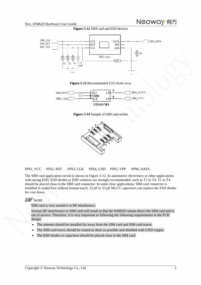
Figure 5-12 SIM card and ESD devices
Figure 5-13 Recommended ESD diode array
Figure 5-14 Sample of SIM card socket
PIN1, VCC PIN2, RST PIN3, CLK PIN4, GND PIN5, VPP PIN6, DATA
The SIM card application circuit is shown in Figure 5-12. In automotive electronics or other applications with strong ESD, ESD diodes or ESD varistors are strongly recommended, such as T1 to T4. T1 to T4 should be placed close to the SIM card connector. In some clear applications, SIM card connector is installed in sealed box without human touch. 22 pF to 33 pF MLCC capacitors can replace the ESD diodes for cost down.
SIM card is very sensitive to RF interference. Serious RF interference to SIM card will result in that the WM620 cannot detect the SIM card and is out of service. Therefore, it is very important to following the following requirements in the PCB design: The antenna should be installed far away from the SIM card and SIM card traces. The SIM card traces should be routed as short as possible and shielded with GND copper. The ESD diodes or capacitors should be placed close to the SIM card.

Neo_WM620 Hardware User Guide
Copyright © Neoway Technology Co., Ltd 4
5.5 USB Interface
Table 5-4 USB interface
Pin Signal I/O Function Remarks
18 USB D+ I/O High-speed USB differential data, (+)
19 USB D- I/O High-speed USB differential data, (-)
20 V_USB PWR USB Power Input voltage 3.3 to 5.5 V.
The WM620 module is compliant with USB2.0 full speed device. The USB2.0 specification requires that the hosts such as PCs support three USB speeds: low-speed (1.5 Mbit/s), full-speed (12 Mbit/s) and high-speed (480Mbit/s).
The V_USB pin is an analog input. A 4.7 µF decoupling MLCC capacitor to GND is strongly recommended, and should be placed as close as possible to the V_USB pin. It will increase the USB stability. ESD diodes should be installed close to these three signals.
Figure 5-15 Reference design for USB interfaces
The layout design of this USB should comply with the USB 2.0. The traces of USB_D+ and USB_D- must be routed as a group of differential pair with 90Ω
differential impedance. The USB differential pair should be routed side-by-side and on the same layer. USB_D+ and D- is a pair of high speed signals, so the trace lengths should match as well as
possible. USB interface must be connected or set aside the relevant test points to facilitate subsequent
firmware upgrade or debugging.
5.6 UART Pin Signal I/O Function Remarks
52 CTS I High-speed UART to send data
53 RTS O High-speed UART ready for receive data
54 RXD I High-speed UART receive data input (allow input 3 V)
55 TXD O High-speed UART transmit data output

Neo_WM620 Hardware User Guide
Copyright © Neoway Technology Co., Ltd 5
5.6.1 Basic Descriptions of UART UART is for AT commands, data sending/receiving, etc.
As a DCE device, the module is connected to DTE, supporting baud rates 1200, 2400, 4800, 9600, 19200, 38400, 57600, 115200, 230400 bit/s, and the default value is 115200.
Figure 5-16 Connection between DCE (module) and DTE
The UART of WM620 works at 2.6 V CMOS logic level. The voltages for input high level should not exceed 3.0 V.
5.6.2 Level Translators for UART If the UART is interfaced with an MCU that has 3.3 V logic levels, resistors should be connected in series with the signal traces, as shown in Figure 5-17.
Figure 5-17 Interfaced with 3.3 V logic levels of MCU
If the UART is interfaced with an MCU that has 5 V logic levels, general level translators are required for both inputs and outputs.

Neo_WM620 Hardware User Guide
Copyright © Neoway Technology Co., Ltd 6
Figure 5-18 Interfaced with 5 V logic levels of MCU
Reference components: R2: 2K-10K. The higher rate the UART works at, the smaller value used. R3: 4.7K-10K. The higher rate the UART works at, the smaller value used. Q1: MMBT3904 or MMBT2222. High-speed transistors are preferred.
Used for 5 V logic > 2.6 V logic:
While the circuit used between MCU TXD and module RXD, the INPUT pin is connected to MCU TXD, and OUTPUT connected to module RXD. VCC_IN is powered by 5 V and VCC_OUT is powered by 2.6 V (module's VDD_2.6V).
Used for 2.6 V logic > 5 V logic:
It can be used between module TXD and MCU RXD as well, with INPUT connected to module TXD, and OUTPUT connected to MCU RXD. VCC_IN is powered by 2.6 V (module's VDD_2.6V) and VCC_OUT is powered by 5 V. This applies to RING signal as well.
Avoid sparks and glitches on UART signals while the module is in the power on procedure. Avoid sending any data to UART during the beginning of 2 seconds after the module is turned on.
5.7 Audio interface
Table 5-5 Audio interface
PIN Signal I/O Function Remarks
28 EAR_1P AO Earphone amplifier output (+) 32Ω Earpiece; typical: 35 mW
29 EAR_1N AO Earphone amplifier output (-)
30 MIC_1N AI Microphone #1 input (-)

Neo_WM620 Hardware User Guide
Copyright © Neoway Technology Co., Ltd 7
31 MIC_1P AI Microphone #1 input (+)
The typical audio interfaces of WM620 are shown in Figure 5-19. The earpiece output pins are directly connected to the earpiece, each with its own bypass capacitor. The capacitor value is selected to optimize performance in each design, but a value of 100 pF or less is expected (100 pF is used in the example). The output power for the differential ear output is typically 35 mW for a full-scale +3 dBm sine wave into a 32 Ω speaker.
Figure 5-19 Microphone connection
6 Mechanics, Mounting and Packaging 6.1 Assembly The WM620 introduces the 62-pin LCC castellation technology. With the features of less pins and wide pitch, WM620 is very suitable for low-cost and simple designs with 2layer PCB. Due to its ultra-compact size and high reliability, it is easy to put WM620 in design. Moreover, WM620 supports manual soldering, adapts to mass production and also low quantity perfectly, and has low technical requirements for manufacturing equipment.
6.2 Packaging and Soldering In order to prevent the product of from being affected with damp, caused by using the SMT way to perform the furnace welding, we employ damp-proof packing, such as Aluminum Foil Bag, desiccating agent, Humidity Indicator Cards, Suck plastic trays, and vacuolization in the process of production and use of the costumer. As a result, the product is kept dry and its life span will be long.
For more storage and SMT information, please refer to Neoway Modules Recommendation for SMT and Reflow Solder.
7 Abbreviations ADC Analog-Digital Converter
AFC Automatic Frequency Control

Neo_WM620 Hardware User Guide
Copyright © Neoway Technology Co., Ltd 8
AGC Automatic Gain Control
AMR Acknowledged multirate (speech coder)
CSD Circuit Switched Data
CPU Central Processing Unit
DAI Digital Audio interface
DAC Digital-to-Analog Converter
DCE Data Communication Equipment
DSP Digital Signal Processor
DTE Data Terminal Equipment
DTMF Dual Tone Multi-Frequency
DTR Data Terminal Ready
EFR Enhanced Full Rate
EGSM Enhanced GSM
EMC Electromagnetic Compatibility
EMI Electro Magnetic Interference
ESD Electronic Static Discharge
ETS European Telecommunication Standard
FDMA Frequency Division Multiple Access
FR Full Rate
GPRS General Packet Radio Service
GSM Global Standard for Mobile Communications
HR Half Rate
IC Integrated Circuit
IMEI International Mobile Equipment Identity
LCD Liquid Crystal Display
LED Light Emitting Diode
MS Mobile Station
PCB Printed Circuit Board
PCS Personal Communication System
RAM Random Access Memory
RF Radio Frequency
ROM Read-only Memory
RMS Root Mean Square

Neo_WM620 Hardware User Guide
Copyright © Neoway Technology Co., Ltd 9
RTC Real Time Clock
SIM Subscriber Identification Module
SMS Short Message Service
SRAM Static Random Access Memory
TA Terminal adapter
TDMA Time Division Multiple Access
UART Universal asynchronous receiver-transmitter
VSWR Voltage Standing Wave Ratio