near east universitydocs.neu.edu.tr/library/1575633787.pdf · chapter three 3.0 pia (peripheral...
TRANSCRIPT

•
Near East University
Computer Engineering Department
Special project Con1400
Practical Implementation Of Memory Interfacing
Advisor: Halli Adahan
Prepared By : Mohammed Omer Almasrl
June 1995

I /
/
•
TABLE OF CON1~ENT
Acknowledgment
Introduction
Table of Content
Cha1>ter ONE
1.0 Microprocessors
1.1 A Brief History Of MP's
1.2 The Motorola MC6800 MP's
1.3 A Typical MC6800 MP system
1.4 The MC6800 Pin Diagram and Functions
1.5 Microprocessor Interfacing
1.6 Interfacing With ROM
1.7 Interfacing With RAM
1
1
3
4
6
8
9
11
Cha})ter TWO
2.0 Memory
2.1 Introduction
2.2 ROM
2.3RAM
2.4 2K x 8 RAM Pin Diagram
13
13
13
14
16

Chapter THREE
3.0 PIA (Peripheral Interface Adapter) 18
3.1 Introduction 18
3.2 The 6821 PIA Block Diagram & Function Description 19
3.3 Architecture Of The PIA 23
3.4 Registers Of The PIA 25
3.5 Peripheral Data Lines & Data Registers 26
3.6 Configuration Of The PIA 29
3.7 Addressing The PIA 29
3.8 Programming V/ith PIA 31
Chapter FOUR
4.0 Discussing The Work Done
Conclusion
32
34
35
64
65
Appendix I
Appendix II
References
•
Acknowledgment
I would like to thank Mr. Kalil Adahan for his kind help and
advice which helped me a lot in doing this project.
I would like to express my gratitude to all people who offered
their advice including Mutaz Elmaki, Sarni Omer, Hulya Almasri .
Finally, it is difficult to acknowledgment ever one for his
valuable suggestions, efforts and/pr remarks. Thanks To them all.

Memory is another image for the human memory, it does the
same process from storing and deleting the information, with the advantage of
that the processed information within the memory is kept in the storage until it
has to be deleted intentionally, mean while the human memory is sometimes
storing the information temporary without intention.
During the last decade, the information processing has been increasing
very rapidly and the demand for memories with high capacity at :information
processing and storage bas consequently increased. In this project I introduced
the interfacing of memories to allow a microprocessor system to have more
memory locations than the microprocessor is capable at addressing using some
techniques.

•
Chapter ONE
1.0 Microprocessors
1.1 A BRIEF HISTORY OF MICROPROCESSORS
The digital computer is controlled by a program, the program tells the
digital computer how to process data .... etc. It does this by using the digital
computer calculation logic, memory circuit, and input/output device, which is
called digital computer architecture. The microprocessor has architecture
similar to the digital computer.
In 1950s, the first general-purpose digital computer appeared. They used
vacuum tubes models were used to build basic circuit such as gates and flip
flops. By assembling gate and flip-flops built the computers calculating logic
and memory circuits. Nevertheless, the early computers introduced important
idea of program storage. Later design provided computer with program
storage.
Solid-state circuit technology also made great strides during 1950s. The
knowledge of semiconductors increased. Naturally, the designers of digital
computers jumped at the chance to replace vacuum tubes with transistor. In the
early 1960s, the art of building solid-state computers advanced. They were
building huge solid-state computers that still required large air-condition
1

rooms. They could process large amount of data. Moving in a new direction •
were smaller companies they began building small computers, about the size of
a disk.
By the early 1960s, the semiconductor industry found away to put a
number of transistors on one silicone wafer. The transistor are connected
together with small metal traces, to perfume a function, such as a gate, flip-
flop, register, or adder. the building blocks or circuit modules made this
way are called an integrated circuit ( IC).
By the mid- l 960s, small-and medium-scale integration ( SSI and MSI )
produced major families of digital logic. The late 1960s and early 1970s saw
large-scale integration ( LSI ). By the 1980s, ve,y large scale integration
(VLSI) gave us I Cs with over 100,000 transistors.
The development of electronic calculator shows the dramatic improvement
in large scale integration. Development achieved great technology such that
assembled to a microprocessor. the microprocessor made possible the
manufacture of powerful calculators and many other products.
Since the early 1970s, the main effort has been to improve the
microprocessor's architecture. Important evaluations of architecture design
increases the microprocessor's speed and computing power. The early
microprocessor processed digital data 4 bits ( 4 binary digits ) at a time. That is
they used a 4-bit word. But new generations of microprocessors came fast.
2

•
The 4-bit microprocessor grew into 8-bit, then into 16-bit, and then into 32-
bit Microprocessors. During the early 1980s, complete 8-bit microprocessor
system (microprocessor with memory and communication ability ) were
developed.
1.2 THE MOTOROLA 1\1C 6800 MPs
The MC6800 microprocessor was introduced by Motorola. it is an 8-bit
microprocessor functionally having an 16-bits address bus. The programming
model for the 6800 is shown in figure 1. Such as 68HC 11, includes an 8-bit
microprocessor, a Timer, ROM, Ram, AID Counter, and a Chip Oscillator. The
functionality-providing also programmable 1/0 lines and an EXROM.
The M6800 is an advanced 16-bit microprocessor. Other member of
Motorola family are the 68HCOOO ( CMOS ), 68008, 68010, 68020, and
68030. The 68000 microprocessor features are 32-bit internal architecture,
with a 16-bit external data bus and it can address 16-MB memory. The 68010
is an update 16-bit external/32 internal virtual memory ( A programmer can
write as if memory capacity is unlimited) MPU. The 68020 support 32 internal
I external.
3

•
1.3 A Typical 6800 Microcomputer System
Restart
Address Bus , 16-bit seoo I Unidirection I..- I MPU I ..__..
--,
t I Data Bus
/ 8-bit Bidirection
ROM • Line
Control RAM • •
PIA PORTB Data Line PORTA
Figure 1
MPU ( Microprocessor Unit)
Inside the MPU there three major functional blocks : ALU (the arithmetic-
logic unit), Data Registers, and the control logic.
4

•
Clocko 1,cp2
cpl: Supply the required clock cycles to increment the internal register
cp2: Provides the necessary clock cycle to fetch and execute an Iinstructure.
ROM: Is a read only memory containing monitor suprotines
display routines tines and timer control subroutines.(see chapter 2).
RAM: Random Access memory RJW where the program is execute
(see chapter 2).
PIA (Peripheral Interface Adapter):
Has two 1/0 ports. Each ports is 8-bit Port A, Port B. Both Port A and
Port B cab be programmed to interface I/0 device (see chapter 3).
System Description
The MC6800 required a +SV power supply and an external two phase
clock (cpl,cp2). The restart input the MC6800 has H/W interrupt connects to the
RESET PIN of the chip. This pin initialized the MPU for start operation. The
MPU has 16 address line and 8 bi-directional data lines. The control lines
added to the system is used to control the timing control how the information
how the information transfer from RAM, ROM, and ALU. The interfacing
between the MPU and the 1/0 devices is done with the PIA The PIA provides
two 8-bit data paths which can be used as input or output ports. The PIA also
has 4 control lines between the PIA and the I/0 devices.
5

• The 6820/6821 PIA has internal register which makes it programmable and
provide temporary storage to simplify the transfer of data. Thus the interrupt
pluses can be send from the PA via the control bus to the MPU. In this way the
PIA forms a two way communication link and a temporary storage device
between the microprocessor and the peripheral device.
1.4 THE MC6800 PIN DIAGRAM AND FUNCTIONS
RESET
~ i~ I TSC
vcc HALT
NC
~
2 MC6800 38 @2
@1 3 IRQ
MPU 37 B= DBE VMA 4 36 ~ NC 5 35 NMII
6
;i I ...•• ~ ~~ BA
7 vcc~ 8
;~ 1: :: g; AO 9 A1 -- 10
30 A2~ 11 29 1:; ~~ A3 12 28 13
27 I~ E00 A4 :=:]
D7 A5 14
26 D8 15 25
A6 3 16 24§15 A7 17
14 AS
23 A13 A9 18 22 A12 A10 19 21 vss 20
The Motorola 6800 is an 8-bit microprocessor placed in 40 bin DIP (Duel
In Line Package).
G

•
PIN Name Description State Type
AO-AlO Address Line TriState, Output, Unidiriction
DO-D7 Data Bus Lines TriState, Bidirection
HALT HALT Input
TSC Three State Control Input
R/W Read/Write Pin TriState, Output
VMA Valid Memory Add. Output
DBE Data Bus Available Input
BA Bus Available Output
IRQ Interrupt Request Input
-- RESET Reset Pin Input
NMI Non Maskable Int. Input
cpl,cp2 Two OverLooping
Clock Signal Input
Vss,VCC Power Input Input
7
•
1.5 l\1ICROPROCESS0R INTERFACING
Most microprocessor in a stand alone fashion don't contain substantial
memory . To increase the power of microprocessor, we have to interface 1/0
modules. The interfacing or leakage, of the port within the system called
interfacing includes synchronization direction of transmission, and sometimes
the adjustment of signal levels.
Interfacing deal with synchronization of data to and from the
microprocessor unit, and there the S I W as well the H I W must be considered
in great detail. Data transfers in and out of the microprocessor unit over the
busses are : -
1- Memory Read
2- Memory write
3- 1/0 Read/Write
4- Interrupt or reset handling
Generally microprocessor is the focus of all operations. But in some case the
MPU releases control of the address and data bus so that the peripheral device
may access the main system memory directly going to the MPU, this is called
DMA.
The MP itself uses MPU, ROM, and RAM externally, and it's of
importance that the manufacturer produce peripheral interface adapters that are
compatible with other MPUs. These are generally general purpose in that they
can programmed to function as either input or output interface programmable
communication device.
8

Manufactures produce specialized interface component IC' s which are
programmable DMA controllers, Programmable interrupt controllers, Diskette
controllers, Synchrouns Data Link controller, and Keyboard display controller.
1.6 INTERFACING WITH ROM
CHIP L
A12-A15 A15 D7 ADDRESS A14 DECODER
.:::
PATA BUS
MPU ~-BIT ADDRESS · D0-D7 BUS AO-A15 J
DO AO_
Pn
,, AO 1/00 >- ~ OE ~ 4K X 8 ROM - -
A11 cs 1/07
J FIG.5
The data bus of MPU' s is connected to the output of the ROM, and the
address bus of the MPU is connected to the address inputs of the ROM.
9

• The simple Red line (RD) output from the MPU is connected to the OE of
the ROM. OE controls the data output from the ROM device. When activated
the outputs of the ROM device is valid and when disabled the outputs of the
ROM device is cut from the data bus. That is there is no response at the output
of the ROM. For the MPU to access data from the ROM it has to set the
address on the address bus frem AO-Al 1, set OE low using the read control-
line, and set the CS line low sing the address decoder. In the MPU model of
6800 the decodes circuit was externally connected to the ROM. The ROM it
self has a decoder mechanism so that, internally it could decode the selected
address coming from the address bus. The CS line is usoo-to select the line chip
to be used. If CS line is hold low, that device is valid to be used.
The functionality of the decoder is great, such that it selects the memory
range to be used. Since there are 4 address line connected to the decoder, there
could be 16 device that could be interfaced to the MPU.
If each ROM device is 4K, this makes a total of 16 x 4K= 64K. But all of
the ROM devices share the same address bus the data bus which is connected
having the same characteristics of the address bus.
Simple configuration of interfacing the address bus and the data bus is the
wired or connection of each parallel line. But this interfacing technique has the
disadvantage that we can not access all the ROM devices at the same time. We
could only use them by address interchange provided by the address decoder.
10

• The advantage is that we could interface more memory units to the MPU by
sampling changing the decoder mechanism.
1.7 INTERFACING WITH RAM
CHIP L
A12-A15 A15 D7 ADDRESS A14 DECODER -
DATA BUS
MPU 8-BIT ADDRESS · DO-D7 BUS AO-A15
DO J
AO_ - WR ~rl
,, AO w R 1/00 - ~ __.. 4KX 8 RAM
- A11 cs 1/07 I
J FIG.5
The interfacing technique is similar to the ROM interface, except that
R/W control line is added to the ~ircuit. The data bus could be programmed in
two ways. The decoder mechanism works in the same way, such that may
RAM modules could be interfaced to the MPU by the modules select line
(MS).
11

• If we want to write to the RAM device, we bring the RD line and the RJW
line low. The 1/0 parts of the RAM are internally programmed as inputs.
Hence, the J\1PU selects the data to be written to the required memory
location and places the address on the address bus. To activate the RAM
device to be used it's selected by address line Al2-Al5. The decoder selected
the appropriate device to be used at the decoder output. Similarly to read from
the RAM, initially WR line is held HIGH so that the I/0 ports of the RAM are
programmed as outputs. Data to be acted on is fitched from the data bus of the
RAM, which is selected from the address line inputs.
12

•
Chapter TWO
2.0MEMORY
2.1 INTRODUCTION
In the previous section, we discussed in detail about l\1P stem .. Each of
these system has a memory. In some systems, the memory is quite small. This
system may only have enough memory locations( or bytes of memory ) to hold
the program and to store a few bytes of variable data.
In this section, we will look at memory hard ware, and both read-write
memory and read-only memory. We will also discuss both dynamic and static
memories and we will give a short definition of three kind of read only
memones.
Finally in this section we will show some memories I I O bin diagram,
decoder and memory organization using two 2K x 8 RAM.
2.2 RAM (Random-Access Read Write Memories)
In today microprocessor, it is found that there is only one type of
addressable memory space, And this is known as the microprocessor main
memory. More ever, it is a R/W memory.
13

• However, there are two major semiconductors technologies to build
integration circuit memories, used today to build memory system in computers,
and these are the Bipolar and the Metal Oxide semiconductor technology.
Bipolar memories are seldom use with microprocessor system. the
advantage of bipolar memories is their very fast access time. They do have a
number of disadvantage when compared with MOS ( Metal Oxide
Semiconductor) memories. They draw a great deal of power, and there fewer
memory bits for the same size silicon chip. The bipolar semiconductor
fabrication process is much more complicated than the MOS process. This
makes bipolar memory much more expensive than MOS memories. For this
reasons, bipolar memories are used only for applications which can introduce
great speeds.
MOS memories is by far the most common microcomputer system. There
are two different ways to construct MOS memories integrated circuits. MOS
memory circuits are either static or dynamic. often, you will see the
abbreviation SRAM ( Static RAM) and DRAM ( Dynamic RAM ) used for
static RAM and dynamic Ram.
Static memory system are simples to build, especially for small memory
system. There are much easier to service. Dynamic memory system use lower
cost integrated circuits but required more support circuits. Also, dynamic
memories must refreshed regularly.
14
• They are usually used in large memory system.
Both static and dynamic semiconductor technologies are steadily
improving. This means than large memories are being made on the same size
silicon wafer. As a result, memory is becoming less expensive.
2.3 ROM ( Read Only Memory)
The read only memory is a memory device which once set with a given bit
pattern, can not be changed. Every microprocessor system must have some
ROM, since every system must have at least enough built-in program to be lead
its RAM with a program from a mass storage device such as magnetic type or
disk.
However, there are three different types of ROM. They are ROM,
EPROM, EEROM. Each of the four types is used for a different application.
ROM is a device with a bit pattern permanently fixed by the semiconductor
manufactures. ROMs are only' used in high-volume applications, because
costume mask designs are expensive. Of course, once a part is masked, it may
never be changed.
EPROM (erasable programmable read-only memory) can be
programmed, erased, and reprogrammed by the user.
15

• Although these devices are somewhat more expensive than ROMs, EPROMs
do let the user change the bit battern as needed. EPROM's are supplied with
microprocessor system whose functions will be changed by the user, by
experience, decide exactly what the system should do.
EEAROM (electrically erasable read only memory). The EAROM can
programmed and altered electrically. Un like the EPROM, the EAROM does
not need an outside device in order to erased.
2.4 RAM 1/0 Pin Diagram & Function
A7 VCC AG AS AS 2K X 8 A9 A4 RAM W/R A3 OE A2 A10 A1 CS AO- 1/08 1/01 1/07 1/02 1/06 1/03 1/05 GND 1/04
In this section we will see the bin diagram of RAM memories the bin
diagram (see fig.in appendix) and expling each bin and it's function.
16

• Pin Name Function
1- AO-AIO Address inputs
2- DO-D7 Data input/output
3- cs Chip Select
4- WE Write enable input
5- OE Output enable input
6- vcc Positive Supply (+5v)
7- GND Negative Supply ( ground)
8- N/C No Connection
17
•
Chapter THREE
3.0 PIA ( Peripheral Interface Adapter)
3.1 Introduction:
The PIA provides the universal means of interfacing peripheral
component to the :MPU. The PIA is capable of interfacing the :MPU to
peripheral to peripheral through two 8-bit bi-directional peripheral data bus and
4 control lines. No external logic is required for interfacing to most peripheral
devices.
The functional configuration of the PIA is programmed by the :MPU during
the system initialization. Each of the peripheral data lines can be programmed
as input and output, and each of the 4 control interrupt lines may be
programmed for one or several control modules. This allows a high flexibility in
the overall operation of the PIA.
18

• 3.2 The 6821 PIA Block Diagram and Function Description.
- CA1
I Interrupt Status L IRQA ~ Control of A CA2 I
Control Register A
IIC:1
(CRA) I ! !;1 Data Direction
00 ; register A 01
Data Bus (DORA) 02 03 Buffers
~~ 111
Output Bus PAO PA1
Output Peripheral PA2 Register A PA3
Interface PA4 (ORA) PA5
A PA6 PA7
Input Bus Bus Input ~r PBO
Peripheral PB1 Register PB2
Interface PB3 PB4
Output
I i i:I 8 PA5 Register B PA6 l~I PA7 vcc (ORB) VS$
cso
cs, 11 CMp Select
~
Data Direction cso register B RSO _._ and R/W (DDRB) RS1 Control Control RNI _._
Register B E (CRB) RES _._
CB1 Interrupt Status IRQB Control of B CB2
The Block Diagram of 6821 PIA
INTERNAL REGISTER
There are six location within the PIA accessible to the MPU data bus : two
Peripheral Register, two Data Direction Register, And two Control Register.
Selection of these locations is controlled by the RSO and RS 1 inputs together
with bit 2 in the Control Register, as shown in table 1.
19

•
Control Regislter Bit
RS1 RSO CRA2 CRB2 Location Selection
0 0 1 X Peripheral Register A
0 0 0 X Data Direction Register A
0 1 X X Control Register A
1 0 X 1 Peripheral Register B
1 0 X 0 Data Direction Register B
1 1 X X Control Reaister B
Table 1
Initialization The PIA
A "Low" reset line has the effect of zeroing all the PIA registers. This will
set PAO .. PA7, PBO .. PB7, CA2 and CB2 as inputs, and all interrupts disabled.
The PIA must be configured during the restart program which follows the
reset.
Data Direction Registers (DDRA and DDRB)
The two Data Direction Register allow the MPU to control the direction of
data through each corresponding peripheral data lines. A Data Direction
Register bit set a "O" configures the corresponding peripheral data line as input;
a "I" results in an output.
20

Control Register (CRA and CRB)
The two Control Register (CRA and CRB) allows the MPU to control the
operation of the four peripheral control lines CAI, CA2, CB 1, CB2. In addition
they allow the MPU to enable the interrupt lines and monitor the status of the
interrupt flags. Bit O through 5 of the two registers may be written or read by
the MPU when the proper chip select and register select signals are applied. Bit
6 and 7 of the two register are read only and are modified by external interrupts
occurring on control lines CAI, CA2, CBI, or CB2. The format of the control
words is shown in table 2.
CRA
7 6 5 I 4 I 3 2 1 I 0
IRQA1 IRQA2 CA2 DRRA CA1 Control Access Control
CRB
7- 6 5 I 4 I 3 2 1 I 0
IRQB1 IRQB2 CB2 DRRB CB1 Control Access Control
Table 2
21

• Data Direction Access Control Bit (CRA2 and CRB2)
Bit 2 in each control register (CRA and CRB) allows selection of either a
Peripheral Interface Register or the Data Direction Register when the proper
register select signals are applied to RSO and RS 1.
Interrupt Flags (CRA6, CRA 7, CRB6, CRB7)
The four interrupt flag bits are set by active transitions of signals on the four
interrupt and Peripheral Control Lines when those lines are programmed to be
inputs. These bits cannot be set directly from the :MPU Data Bus and are reset
indirectly by a Read Peripheral Data Operation on the appropriate section.
Control ofCAl and CBI Interrupt Lines (CRAO, CRBO, CRAl, and CRBl).
The two lowest order bits of the control register are used to control the
interrupt input lines CAI and CB 1. Bits CRAO and CRBO are used to enable
the :MPU interrupt signals IRQA and IRQB, respectively. Bits CRAl and
CRB 1 determine the active transition of the interrupt input signals CAI and
CBI. Control of CA2 and CB2 Peripheral Control Lines ( CRA3, CRA4,
CRAS, CRB3, CRB4, and CRBS).
Bit 3, 4, and 5 of the two control register are used to control the CA2 and
CB2 Peripheral Control Lines. This bits determine if the control lines will be an
interrupt input or an output control signal. if bit CRAS (CRBS) is "O", CA2
(CB2) is an interrupt input lines similar to CAI (CB 1). When CRAS (CRBS) is
"l", CA2 (CB2) becomes an output signal that may be used to control
peripheral data
22

• transfers. When in the output mode, CA2 and CB2 have slightly different
characteristics.
3.3 ARCHITECTURE OF THE PIA
Pin-out of the PIA
0 40
SETA i To and from Peripherals I
"'" ~
••• GND ••• ••• PAO
••• ••• PA1
••• ••• PA2 RESET PA3 DO - - ••• ••• ..• : PA4 D1 - - - PAS
..• : - D2 - ••• ••• PA6 D3 - ...-- - - •••• ••• PA7 D4 - ...--
PBO DS - - •••• ••• - PB1 D6 . - ••• ••• PB2 - ..
D7 - - ••• ••• PB3 - - - ••• •••• PB4 - .. ••• ••• PBS
PB6 ••• ••• PB? __.. +SV R/W ~
To and from Microprocessor via the Data Bus
The figure shows a pin-out of the PIA the PIA has 40 pins, which connect
to the various busses. First, we'll discuss four pins on the control bus that are
inputs to the PIA The PIA has pins that supply its power: +5V and the GND.
The R/W pin is connected to the MPU' s R/W pin and is high when the MPU is
reading from the PIA and low when the MPU is writing to the PIA The PIA
has some internal registers, which we'll descuss later. A low voltage on the
PIA's RESET pin clears all of its registers. (when a register or memory
location is cleared, each bit is cleared to zero).
23

Right now we'll focus our attention on the data pins. The PIA acts as "go
between" for the 6800 and one more peripherals, so it has two kinds of data
pins: one kind for exchanging data with the microprocessor, and other for
exchanging data with peripherals.
The PIA has 8 data pins (DO-D7) for exchanging data with the
microprocessor. There are connected to the 6800,s bi-directional data bus.
In additional, the PIA has 16 peripheral data pins (PAO through PA 7 and
PBO through PB 7) for sending and receiving data to from the peripheral
devices. The peripheral data pins are organized into two sets into two sets of 8,
called set A and set B, corresponding to sides A and B of the PIA
Each Peripheral data line can be either an input or an output of the PIA, but
not both at once. Peripheral data lines are programmed individually to be an
input or an output, depending on what we need. These lines can be all inputs,
all outputs, or any combination.
24

3.4 Registers of the PIA
To Peripherals To Peripherals
Data Line A , ' ' ' ' f f f f T T T T T T T T D~ta Line B
Data Register A ORA
Data Register B ORB
I I I I I I I I I I I I I I I I I I Data Direction Register A
DDRA Deta Direction Register B
DDRB
I I I I I I I I I I I I I I I I I I Control Register A
CRA Control Register B
CRB
The fig shows the registers of the PIA , its data lines, and its registers.
Besides 8 peripheral data lines, each of the A and B sides has three registers.
Although there are subtle differences between the two sides, we won't discuss
those differences in this project. We just look one side, which is side A. For our
purpose we assume that whatever we say about side A goes for side B.
On side A, peripheral data register A, is called Data Register A (DRA), is
an 8-bin register in the PIA that holds the current data to be input or output
from the A side of the PIA.
25

• To determine whether each bit in DRA is used for input or output, we use
Data Direction Register· A (DDRA). If a bit in DDRA is a 1, then the
corresponding bit is DRA will be an output; if 0, an input.
Control Register A (CRA) allows the MPU to control the operation of the
2 peripheral control lines CAl, CA2. In addition it allows the MPU to enable
the interrupt lines and monitor the status of the interrupt flag.
3.5 Peripheral data lines and Data Register A (CRA)
a- Side A of the PIA Using Eight Switches as input
1=1ight on O=light off
Peripheral Data Lines Side A
Peripheral Data Lines Side B
(2) ORA recives inputs data (11000010)
Data Bus ~~~+--t_o_M_P_U ~
Data Bus contains 11000010 (C2)
(3) MPU roads data PIAs Internal Bus PIA
A block diagram showing the communication between side A's peripheral
data lines and a set of 8 switches to be used for input. The MPU can read the
data input on the switches after the data has first passed through the PIA.
26

• Here, "switch up" causes 1 to be input, and "switch down" causes O to be
input. Thus all of switches up would all the MPU to read 11111111 ($FF), and
all switches drown would allow the MPU to read 00000000 ($00).In the above
figure illustrates a typical case. At ( 1) the user inputs the value (in this case,
$C2) on the switches. At (2) the date, $C2, goes to data register A via side A's
peripheral data lines. At (3) the data gets onto the data bus via the PIA's
internal bus. Then the MPU can read the data. In this case side A is set up for
all 8 lines to be inputs. Once we have wired side A for all inputs, it would
naturally stay that way until its rewired.
Alternatively, we could wire side A so that all 8 were outputs. For an
output device, we'll use a Light-Emitting Diode (LED), a small device that
produces a red light when turned on. LED's are very commonly used in
microcomputer displays. An LED can be wired so that a 1 means "light on" and
a O mean "light off'. Or it can be wired in opposite way : 1 = "light off' and O=
"light on".
27

• b- Side a of the PIA Using Eight LED's as Outputs
~-------------, (1)
,o
I Light on
0 Lightoff 1=1ight on O=light off
Peripheral Data Lines Side A
Peripheral Data Lines Side B
ORB MPU writes A7 1) 10100111 onto data bus ~---+---'--'--'-'-. (2)
ORA gets outputs data (A7)
Pl As Internal Bus PIA Data Bus fromMPU
The Figure show's side A of the PIA wired through interface circuitry so
that all 8 peripheral data lines are outputs to 8 LED's. In this case the MPU can
write data into LED's by first passing the data through the PIA Here, a 1
output by the MPU to the PIA causes an outputs of light on, and O causes light
off. So if the MPU writes 11111111 ($FF) all the lights will be turned on. And
the writes 00000000 ($00), all the lights will turned off. The figure showen
above illustrates a particular example. At (l) the MPU places the data ($A7, in
this case) onto the data bus. At (2) the date placed into DRA via the PIAs
internal bus. At (3) the data is output onto the LED's through the PIAs side A
eripheral data lines, and the binary number 10101110 ($A 7) appears as the
pattern on the light.
28
.. We've shown of side A of the PIA being used for inputs and all outputs. But
we can use each line individually for either input or output. We could wire 4
peripheral data line to switches and 4 to LED's or 7 to switches and I to an
LED's or 3 to switches and 4 to LED's, and so on.
3.6 Configuring the PIA
Setting the peripheral data lines of the PIA to be inputs or outputs. Configure
side A of the PIA, we use Data Direction Register A (DDRA) and Control
Register A (CRA).
The Content of DDRA determine whether a peripheral data line is an input
or output: a O means input, and 1 means an output. To set the A side for all
input as we done in fig( ... ), DDRA had to loaded with all ls, or $FF
hexadecimal. Loading different words into the data direction register will cause
possible combinations of inputs and outputs.
3.7 ADDRESSING THE PIA
Each register of the PIA has an address, and it accessed like a memory
location. To load a register in the PIA, we write a number to the register's
address. And to examine the content of the PIA registers, we read the content
of that register's address.
29

• There are six register all together, three on each side. But a PIA requires only
four address: two for each side. The control register has own address. The data
register and data direction register share a single address.
a. Addressing the Control Register
In the previous section we load bit 2 with a O or a 1 to determine whether
we're accessing DRA or DDRA. In this section we will see why DRA and
DDRA both use the same address.
Figure .. .illustrates accessing the control register. Examing location $8005
shows the contents of CRA, which can be change just by loading a different
number into that location.
Some of the other bits in the control registers can be changed in the course
of program execution. Thus we may find that locations $8005 and $8007 have
had some of the contents altered since we loaded them with 00. Typically, bit 2
will not be changed in this fashion. Now CRA is set so that we can get at
DDRA through location $8004.
b. Addressing The Data Direction Register
Once we've cleared CRA, we've assigned address $8004 to DDRA. So
that the content of $8004 (the address of DDRA) determine which of the data
lines will functions as which will function as output.
30

• c. Addressing The Data Register
The data registers have to share address with the data direction registers.
So far, by setting bit 2 of CRA to 0, we've established that location $8004
would access DDRA. But now, we are finished with DDRA and need to access
DRA.
Thus, we go back to CRA and set bit 2 to 1. Then the location $8004 will
address DRA.
3.8 PROGRAMMING WITH PIA
After we know how to address the registers of the PIA, we can begin writing
programs that configure and use the PIA.
a. Reading and Writing in the PIA
The cause the CPU to read the content of a location, we use LDA A or LDA
B. To write into a location, we use ST A A or STA B. Because the registers of
the PIA are all represented by address, writing a program to read and write in
them is easy
31

•
Chapter FOUR
4.0 Discussing The Work Done
In the interfacing mechanism implemented in this project, I started by using
four memories each one 1 KB.
First of all I construct the diagram shown on figure la (see appendix). This
diagram illustrate the connections of the memories. After that I interfaced the
memories with the MPU, then I selected the address busses ( AO to A9)
connected to the memories, and by adjusting the address (AlO and All) to the
2 to 4 decoder ( see Appendix I Fig. la) and leaving the address bus (Al2,
Al3, Al4, Al5) unconnected. This has expand the memory size. 1st RAM is
address from (OOOOH-03 77H), the 2nd RAM is address (0400H-07FFH), the
3rd RAM address (0800H- OBFFH), and the last one address (OCOO-OFFF)
(see Appendix I, Table la). Thus each RAM has 1KB, and the total size for the
four Ram's are 4KB.
However, we change the MPU connection to (All and Al2) and leaving
(AlO, Al3, Al4, Al5) disconnected (see Appendix I, Fig. lb) , by doing we
expanded the memory size. The 1st RAM now is contain address from (
OOOOH-07FFH), the 2nd RAM (0800H-07FFH), the 3rd RAM(lOOOH-17FFH),
and the last one (1800H-1FFFH) (see Appendix lb, Table lb). This time we
increased the
32

• size of the RAM for each one 2KB and we got the total size can mapped for
the 4KB RAM's are 8KB ( see appendix).
More ever, we repeated the some process and changing the decoder poles
to the address (Al2 and A13) leaving address( AlO, All, Al4, Al5)
disconnected (see Appendix I, Fig le) . This process has increased the memory
size for each one. The 1st RAM now is contain address (OOOOH-OFFFH), the
2nd Ram address (lOOOH-lFFFH), the 3rd RAM (2000H-2FFFH), and the last
RAM (3000H-3FFF) (see Appendix I, Table le). And has expand the memory
capacity to 4KB for each RAM, and the total capacity can access the 4 RAM' s
are 16KB.
We carry on completing the decoder poles to the address bus and we found
that each time the memory size increases every time until it reached it's
maximum size 16KB for each one. for more detail about the result (see
appendix I) .
Moreover, I used a 2KB (see Appedix I, Fig. & Table 2a, 2b, 2c, 2d)
memories, 4kB (see Appendix I, Fig. & Table 3a, 3b, 3c, )) memories and
16KB (see Appendix I, Fig. & Table, 4a) memories. And repeating the process
I used in the beginning, this process has successful expand our memory
capacity. The result of this project steps are shown in (appendix I).
By implementing this process practically in the lab, we found that our
results are consistent to the theoretical figures. The practical connection of the
:MPU, 2K X 8 RAM as shown in (see Appendix I, Fig. Sa). And illustrated that
our work was successfully accomplished.
33

•
Conclusion
The last decays of 20th century the demand of storage system has increased,
hence a demand for information storage system has consequently grown. The
MPU system has been developed. In this project we interface the MPU to
RAM/ROM to increase the size of memory, and this was done successfully by
using the decoder mechanism. We interface all size of memory units to the
MPU and by changing the connection of the MPU to the decoder we managed
to increase the size of the memory successfully.
34

•
APPENDIX I
35

I Fig.1al INTERFACING WITH 1 K X 8 RAM
WM# c\.15 Al4 Al3 A12 AllAIOA9A8 A7 A6 AS A4 A3 A2 Al AO ADDRESS
1 0 0 0 0 0 0 0 (I () (I (I 0 0 0 0 0 0000 H 0 (I 0 0 () () I 1 1 1 1 1 1 1 1 1 03FFH
2 0 0 0 0 0 I 0 0 (I 0 0 0 0 0 0 0 0400 H 0 0 (I (I 0 1 l 1 1 1 1 1 1 1 1 1 07FFH
3 0 0 0 0 I (I () 0 0 () 0 0 () 0 0 0 0800 H 0 0 () () 1 () 1 1 1 1 I 1 1 1 1 1 OBFFH
4 0 () 0· () 1 1 0 () 0 (I (I 0 (I (I () 0 OCOO H 0 (I 0 (I 1 1 1 1 1 1 1 1 1 1 1 1 OFFFH
Table la
Note : Eeach RAM contain lK, and the total area is 4 KB
36

INTERFACING WITH 1 K X 8 RAM
Fig. lb
37

ROM# AIS Al4 A13 Al2 All AlO A9 A8 A7 A6 A5.A4 A3 A2 Al AO ADDRESS
0 0 0 0 0 0 0 0 0 0 0 0 0 0 0 0 OOOOH
0 0 0 0 0 0 1 1 1 1 1 1 1 1 1 1 03FFH
I 0 0 0 0 0 1 0 0 0 0 0 0 0 0 0 0 0400H
0 0 0 0 0 1 1 1 1 1 1 1 1 1 1 1 07FFH
0 0 0 0 1 0 0 0 0 0 0 0 0 0 0 0 0800 H 0 0 0 0 1 0 1 1 1 1 1 1 1 1 1 1 OBFFH
2 0 0 0 0 1 1 0 0 0 0 0 0 0 0 0 0 OCFFH 0 0 0 0 1 1 1 1 1 1 1 1 1 1 1 1 OFFFH
0 0 0 1 0 0 0 0 0 0 0 0 0 0 0 0 1000H 0 0 0 1 0 0 1 1 1 1 1 1 1 1 1 1 13FFH
3 0 0 0 1 0 1 0 0 0 0 0 0 0 0 0 0 1400H 0 0 0 1 0 1 l 1 1 1 1 1 1 1 1 1 17FFH
0 0 0 1 1 0 0 0 0 0 0 0 0 0 0 0 1800H 0 0 0 1 1 0 1 1 1 1 1 1 1 1 1 1 lBFFH
4 0 0 0 1 1 1 0 0 0 0 0 0 0 0 0 0 lCOOH 0 0 0 1 1 1 1 1 1 1 1 1 1 1 1 1 lFFFH
Table lb
NOTE : Eeach RAM contain 2K, and the total area is 8 KB
38

j Fig. 1c J INTERFACING WITH 1K X 8 RAM
39

~ ROM# Al5 Al4 A13 Al2 All AlO A9 A8 A7 A6 AS A4 A3 A2 Al AO ADDRESS
0 0 0 0 0 0 0 0 0 0 0 0 0 0 0 0 OOOOH 0 0 0 0 0 0 1 1 1 1 1 1 1 1 1 1 03FFH
0 0 0 0 0 1 0 0 0 0 0 0 0 0 0 0 0400H 0 0 0 0 0 1 1 1 1 1 1 1 1 1 1 1 07FFH
I 0 0 0 0 1 0 0 0 () 0 () () 0 0 0 0 0800H 0 0 0 0 1 0 1 1 1 1 1 1 1 1 1 1 OBFFH
0 0 0 0 1 1 0 0 0 0 0 0 0 0 0 0 OCOOH 0 0 0 0 1 1 1 1 1 1 1 1 1 1 1 1 OFFFH
0 0 0 1 0 0 0 0 0 0 0 0 0 0 0 0 1000H 0 0 0 1 0 0 1 1 1 1 1 1 1 1 1 1 13FFH
0 0 0 1 0 1 0 0 0 0 0 0 0 0 0 0 1400H
0 0 0 1 0 1 1 1 1 1 1 1 1 1 1 1 17FFH
2 0 0 0 1 1 0 0 0 0 0 0 0 0 0 0 0 1800H 0 0 0 1 1 0 1 1 1 1 1 1 1 1 1 1 lBFFH
0 0 0 1 1 1 0 0 0 0 0 0 0 0 0 0 lCOOH 0 0 0 1 1 1 1 1 1 1 1 1 1 1 1 1 lFFFH
0 0 1 0 0 0 0 0 0 0 0 0 0 0 0 0 2000H 0 0 1 0 0 0 1 1 1 1 1 1 1 1 1 1 23FFH
0 0 1 0 0 1 0 0 0 0 0 0 0 0 0 0 2400H 0 0 1 0 0 1 1 1 1 1 1 1 1 1 1 1 27FFH
3 0 0 1 0 1 0 0 0 0 0 0 0 0 0 0 0 2800H 0 () 1 0 1 - 0 1 1 1 1 1 1 1 1 1 1 2BFFH
0 0 1 0 1 1 0 0 0 0 0 0 0 0 0 0 2COOH 0 0 1 0 1 1 1 1 1 1 1 1 1 1 1 1 2FFFH
0 0 1 1 0 0 0 0 0 0 0 0 0 0 0 0 3000H
0 0 1 1 0 () 1 1 1 1 1 1 1 1 1 1 33FFH
4 0 () 1 1 0 1 () 0 () () 0 () 0 0 () () 3400H 0 () 1 1 () 1 1 1 1 1 1 1 1 1 1 1 37FFH
0 () 1 1 1 0 0 0 0 () () () () () () 0 3800H 0 () 1 1 1 0 1 1 1 1 1 1 1 1 1 1 3BFFH
() 0 1 1 1 l 0 0 0 0 0 0 0 0 0 0 3COOH 0 0 1 1 1 1 1 1 1 1 1 1 1 1 1 1 3FFFH
Table le NOTE : Eeach RAM contain 4K, and the total area is 16 KB

I Flg.1d I INTERFACING WITH 1K X 8 RAM
41
ROM# Al5 A14 A13 Al2 All AlO A9 A8 A7 A6 A5AA4 A3 A2 Al AO ADDRESS
0 0 0 0 0 0 0 0 0 0 0 0 0 0 0 0 OOOOH 0 0 0 0 0 0 1 1 1 1 1 1 1 1 1 1 OJFFH
0 0 0 0 0 1 0 0 0 0 0 0 0 0 0 0 0400H 0 0 0 0 0 1 1 1 1 1 1 1 1 1 1 1 07FFH
0 0 0 0 I 0 0 0 0 0 0 0 0 0 0 0 0800H 0 0 0 0 I 0 1 I I 1 1 I 1 1 1 1 OBFFH
0 0 0 0 I 1 0 0 0 0 0 0 0 0 0 0 OCOOH 0 0 0 0 1 1 1 1 1 1 1 1 1 1 1 1 OFFFH
1 0 0 0 1 0 0 0 0 0 0 0 0 0 0 0 0 1000H 0 0 0 1 0 0 1 1 1 1 1 1 1 1 1 1 13FFH
0 0 0 1 0 1 0 0 0 0 0 0 0 0 0 0 1400H 0 0 0 1 0 1 1 1 1 1 1 1 1 1 1 1 17FFH
0 0 0 1 1 0 0 0 0 0 0 0 0 0 0 0 1800H 0 0 0 1 1 0 I 1 1 1 1 I 1 1 1 1 lBFFH
0 0 0 I I I 0 0 0 0 0 0 0 0 0 0 lCOOH 0 0 0 1 1 1 1 1 1 1 1 1 1 1 1 1 lFFFH
0 0 1 (I 0 0 0 0 0 0 0 0 0 0 0 0 2000H 0 0 1 0 0 0 1 1 1 1 1 1 1 1 1 1 23FFH
0 0 1 0 0 1 0 0 0 0 0 0 0 0 0 0 2400H 0 0 1 0 0 1 I 1 1 1 1 1 1 1 1 1 27FFH
0 0 1 0 1 0 0 0 0 0 0 () 0 0 () () 2800H (I 0 I 0 I () 1 I I I I 1 I 1 1 1 2BFFH
0 0 1 0 1 1 0 0 0 0 0 0 0 0 0 0 2COOH () 0 1 0 1 1 1 1 1 1 1 1 1 1 1 1 2FFFH
2 0 (I 1 1 0 0 0 0 0 0 0 0 0 0 0 0 3000H 0 () 1 1 0 0 1 1 1 1 1 1 1 1 1 1 JJFFH
0 (I 1 1 0 1 0 0 0 0 0 0 0 0 0 0 3400H 0 0 1 1 0 1 I 1 1 1 1 1 1 1 1 1 37FFH
0 0 1 1 1 0 0 0 0 0 0 0 0 0 0 0 3800H 0 0 1 I 1 0 1 1 I 1 1 1 1 1 I 1 JBFFH
0 0 1 1 1 1 0 0 0 0 0 0 0 0 (I 0 JCOOH 0 0 1 1 1 I 1 1 1 1 1 1 1 1 1 1 JFFFH
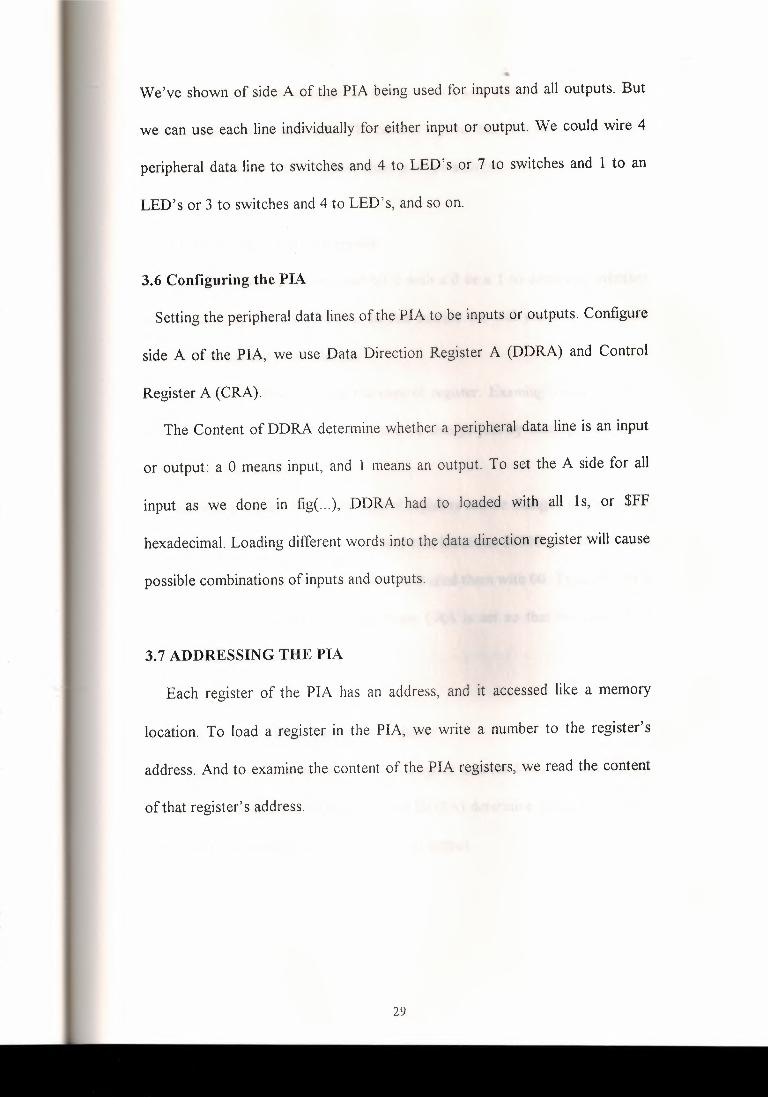
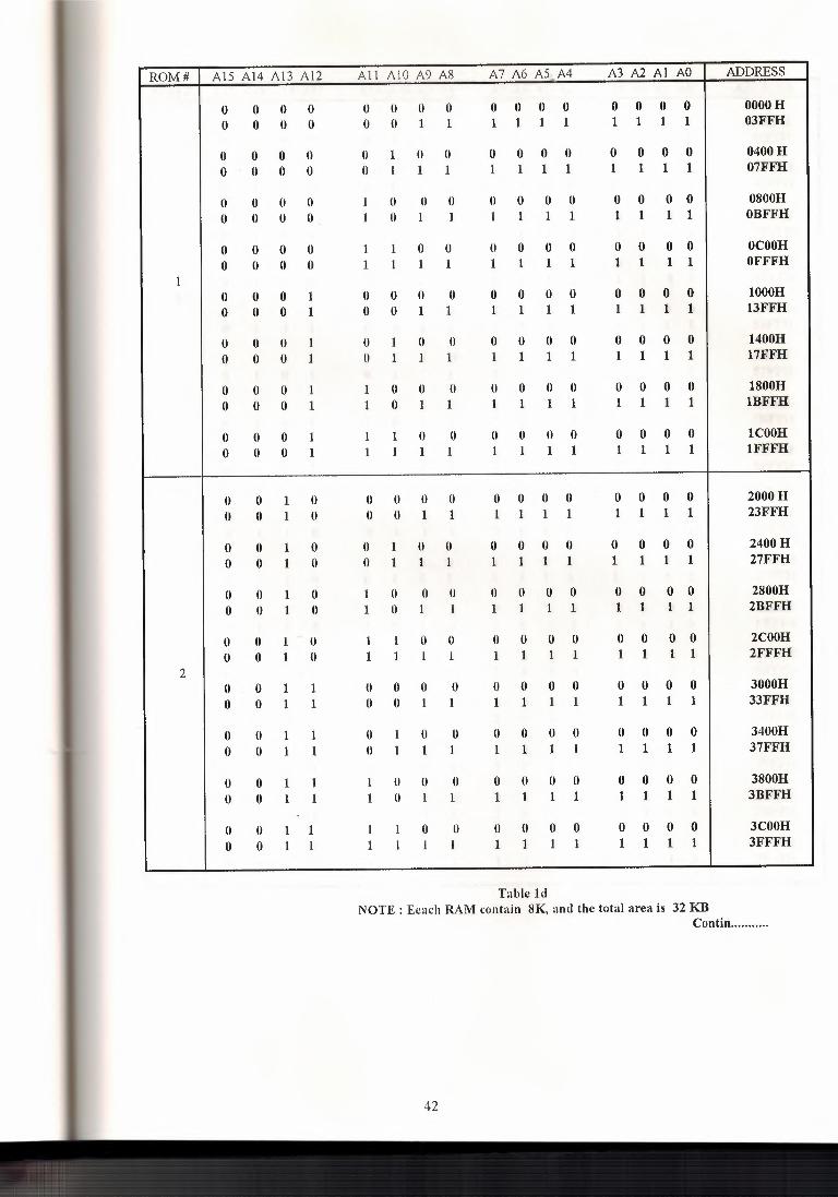
Table ld NOTE : Eeach RAM contain 8K, and the total area is 32 KB
Con tin .
42

ROM# Al5 Al4 Al3 A12 All AlO A9 A8 A7 A6 A5 A4 A3 A2 Al AO ADDRESS
0 1 0 0 0 0 0 0 0 0 0 0 0 0 0 0 4000H 0 1 0 0 0 0 1 1 1 1 1 1 1 1 1 1 43FFH
0 1 0 0 0 1 0 0 0 0 0 0 0 0 0 0 4400 H 0 1 0 0 0 1 1 1 1 1 1 1 1 1 1 1 47FFH - 0 1 0 0 1 0 (I (I 0 (I (I (I 0 0 0 0 4800H 0 1 0 (I 1 (I l 1 1 1 1 1 1 1 1 1 4BFFH
0 1 0 0 I 1 0 0 0 (I (I 0 0 0 0 0 4COOH 0 1 (I (I 1 1 1 1 1 1 1 1 1 1 1 1 4FFFH
3 0 1 0 1 0 0 0 0 (I 0 0 0 0 0 0 0 5000H 0 1 0 1 0 0 1 I 1 1 1 1 1 1 1 1 53FFH
0 1 0 1 0 1 0 0 (I 0 0 0 0 0 0 0 5400H
0 1 (I 1 0 I 1 1 I 1 1 1 1 1 1 1 57FFH
0 1 (I 1 1 0 (I 0 (I 0 0 0 0 0 0 0 5800H 0 1 0 1 1 (I 1 1 1 1 1 1 1 1 1 1 5BFFH
0 1 0 1 1 1 0 0 0 (I (I 0 0 0 0 0 5COOH 0 1 0 1 I I 1 1 1 1 1 1 1 1 1 1 5FFFH
0 1 1 0 (I () 0 (I (I 0 (I 0 0 0 0 0 6000H 0 1 I (I 0 (I 1 I 1 1 1 1 1 1 1 1 63FFH
0 1 1 0 0 1 (I (I 0 0 (I 0 0 0 0 0 6800H 0 1 1 0 (I 1 1 1 1 1 1 1 1 1 1 1 67FFH
0 1 1 0 1 (I 0 (I 0 (I 0 0 0 0 0 0 6800H 0 1 1 (I 1 0 1 I 1 1 1 1 1 1 1 1 6BFFH
0 1 1 (I 1 l 0 (I 0 0 0 0 0 0 0 0 6COOH (I 1 I 0 I 1 I I I 1 1 1 1 1 1 1 6FFFH
4 0 1 1 1 () (I (I 0 0 0 (I (I 0 0 0 0 7000H 0 1 1 1 (I 0 I 1 1 1 1 1 1 1 1 1 73FFH
0 1 1 1 (I 1 0 0 0 0 0 0 0 0 0 0 7400H 0 1 1 1 0 1 1 1 1 1 1 1 1 1 1 1 77FFH
0 1 1 1 1 0 0 0 0 0 0 0 0 0 0 0 7800H 0 1 1 1 1 0 1 1 1 1 1 1 1 1 1 1 7BFFH
0 1 1 1 1 I 0 0 0 0 0 0 0 0 0 0 7COOH 0 1 I 1 1 I I 1 1 1 1 1 1 1 1 1 7FFFH
43

I Fig. 1e j INTERFACING WITH 1K X 8 RAM
44

ROM# AlS Al4 Al3 Al2 All AlO A9 A8 A7 A6 A5~A4 A3 A2 Al AO ADDRESS
0 0 0 0 0 0 0 0 0 0 0 0 0 0 0 0 OOOOH
0 0 0 0 0 0 1 1 1 1 1 1 1 1 1 1 03FFH
0 0 0 0 0 1 0 0 0 0 0 0 0 0 0 0 0400H 0 0 0 0 0 1 1 1 1 1 1 1 1 1 1 1 07FFH
0 0 0 0 1 0 0 0 0 0 0 0 0 0 0 0 0800H 0 0 0 0 1 0 1 1 1 1 1 1 1 1 1 1 OBFFH
0 0 0 0 1 1 0 0 0 0 0 0 0 0 0 0 OCOOH 0 0 0 0 1 I 1 1 1 1 1 1 1 1 1 1 OFFFH
0 0 0 1 0 0 0 0 0 0 0 0 0 0 0 0 1000H 0 0 0 1 0 0 1 1 1 1 1 1 1 1 1 1 13FFH
0 0 0 1 0 1 0 0 0 0 0 0 0 0 0 0 1400H 0 0 0 1 0 1 1 1 1 1 1 1 1 1 1 1 17FFH
0 0 0 1 1 (I (I 0 (I 0 (I 0 (I (I 0 0 1800H 0 0 (I 1 1 0 1 1 1 1 1 1 1 1 1 1 lBFFH
0 0 0 1 1 1 0 0 0 0 0 0 0 0 0 0 lCOOH 1 0 0 0 1 1 1 1 1 1 1 1 1 1 1 1 1 lFFFH
0 0 1 0 0 0 0 0 0 0 0 0 0 0 0 0 2000H 0 0 1 0 0 0 1 1 1 1 1 1 1 1 1 1 23FFH
0 0 1 0 0 1 0 0 0 0 0 0 0 0 0 0 2400H 0 0 1 0 0 1 1 1 1 1 1 1 1 1 1 1 27FFH
0 0 1 0 1 0 0 0 0 0 0 0 0 0 0 0 2800H 0 0 1 0 1 0 1 1 1 1 1 1 1 1 1 1 2BFFH
0 0 1 0 1 1 0 () 0 0 0 0 0 0 0 0 2COOH 0 () 1 () 1 1 1 1 1 1 1 1 1 1 1 1 2FFFH
() 0 1 1 0 0 0 0 () 0 0 0 0 0 0 0 3000H 0 0 1 1 0 0 1 1 1 1 1 1 1 1 1 1 33FFH
0 () 1 1 0 1 0 0 0 0 () 0 0 0 0 () 3400H 0 () 1 1 0 1 1 1 1 1 1 1 1 1 1 1 37FFH
0 0 1 1 1 0 0 u 0 0 0 0 0 0 0 0 3800H 0 0 1 1 1 0 1 1 1 1 1 1 1 1 1 1 3BFFH
0 0 1 1 1 1 0 0 0 0 0 0 0 0 0 0 3COOH 0 0 1 1 1 1 1 1 1 1 1 1 1 1 1 1 3FFFH
Table le NOTE : Ecach RAM contain 16K, and the total area is 64 KB
Continu .
45

ROM# Al5 Al4 Al3 Al2 AllAlOA9A8 A7 A6 A5 _A4 A3 A2 Al AO ADDRESS
0 1 0 0 0 0 0 0 0 0 0 0 0 0 0 0 4000H
0 1 0 0 0 0 1 1 1 1 1 1 1 1 1 1 43FFH
0 1 0 0 0 1 0 0 0 0 0 0 0 0 0 0 4400H
0 1 0 0 0 1 I 1 1 1 1 1 1 1 1 1 47FFH
0 1 0 0 I 0 0 0 0 0 0 0 0 0 0 0 4800H 0 1 0 0 1 0 1 1 1 1 1 1 1 1 1 1 4BFFH
0 1 0 0 1 I 0 0 0 0 0 0 0 0 0 0 4COOH 0 1 0 0 1 1 1 1 1 1 1 1 1 1 1 1 4FFFH
0 1 0 1 0 0 0 0 0 0 0 0 0 0 0 0 SOOOH 0 1 0 1 0 0 I 1 1 1 1 1 1 1 1 1 53FFH
0 1 0 1 0 1 0 (I (I 0 0 0 0 0 0 0 5400H 0 1 0 1 0 1 1 I 1 1 1 1 1 1 1 1 57FFH
0 1 0 1 1 0 0 0 0 0 0 0 0 0 0 0 5800H 0 1 0 1 1 0 1 1 1 1 1 1 1 1 1 1 SBFFH
0 1 0 I 1 1 0 0 0 0 0 0 0 0 0 0 SCOOH 2 0 I 0 I 1 1 I 1 1 1 1 1 1 1 1 1 SFFFH
0 1 1 0 0 0 0 0 0 0 0 0 0 0 0 0 6000H 0 1 1 0 0 0 I 1 1 1 1 1 1 1 1 1 63FFH
0 1 1 0 0 1 0 0 0 0 0 0 0 0 0 0 6400H 0 1 1 0 0 1 1 1 1 1 1 1 1 1 1 1 67FFH
0 I 1 Cl 1 0 0 Cl Cl Cl 0 Cl Cl 0 Cl 0 6800H 0 I 1 0 1 0 1 1 I 1 1 1 1 1 1 1 6BFFH
0 1 I Cl I 1 0 0 0 0 0 0 0 0 0 0 6COOH 0 1 I 0 I 1 1 I 1 1 1 1 1 1 1 1 6FFFH
0 1 I 1 0 0 0 0 0 0 0 0 0 0 0 0 7000H 0 1 1 1 0 0 1 1 1 1 1 1 1 1 1 1 73FFH
0 1 1 1 0 1 0 0 0 0 0 Cl 0 0 Cl 0 7400H 0 1 1 1 0 1 1 1 1 1 1 1 1 1 1 1 77FFH
0 1 1 1 1 0 0 0 0 0 0 Cl Cl 0 Cl 0 7800H 0 1 1 1 1 0 I 1 I 1 1 1 1 1 1 1 7BFFH
0 1 I 1 1 I 0 Cl 0 Cl 0 0 0 Cl 0 0 7COOH 0 1 I I I l 1 I I I 1 1 1 1 1 1 7FFFH
Continu .
46

ROM# Al5 Al4 Al3 Al2 All AlO A9 A8 A7 A6 A5_A4 A3 A2 Al AO ADDRESS
1 0 0 0 0 0 0 0 0 0 0 0 0 0 0 0 8000H
1 0 0 0 () 0 1 1 1 1 1 1 1 1 1 1 83FFH
1 0 0 0 0 1 0 0 0 0 0 () 0 0 0 0 8400H
1 0 0 0 () 1 1 1 1 1 1 1 1 1 1 1 87FFH
1 0 0 0 ·1 (} 0 0 0 0 (} (} 0 0 0 0 8800H
1 0 0 0 1 0 1 1 1 1 1 1 1 1 1 1 8BFFH
1 0 0 0 1 1 0 0 0 0 0 (} 0 0 0 0 8COOH
1 0 0 0 1 1 1 1 1 1 1 1 1 1 1 1 8FFFH
1 0 0 1 0 0 0 0 0 0 0 0 0 0 0 0 9000H
1 0 0 1 0 0 1 1 1 1 1 1 1 1 1 1 93FFH
1 0 0 1 0 1 0 0 0 (} 0 0 0 0 (} 0 9400H
1 0 0 1 0 1 1 1 1 1 1 1 1 1 1 1 97FFH
1 0 0 1 1 0 0 0 0 (} 0 0 (} 0 0 0 9800H
1 0 0 1 1 0 1 1 1 1 1 1 1 1 1 1 9BFFH
1 0 0 1 1 1 0 0 0 0 0 0 0 (} 0 0 9COOH
3 1 0 0 1 1 1 1 1 1 1 1 1 1 1 1 1 9FFFH
1 0 1 0 0 0 0 0 0 0 0 0 0 0 0 0 AOOOH
1 0 1 0 0 0 1 1 1 1 1 1 1 1 1 1 AJFFH
1 0 1 0 0 1 0 0 0 0 0 0 0 0 0 0 A400H
1 0 1 0 0 1 1 1 1 1 1 1 1 1 1 1 A7FFH
1 0 1 0 1 0 0 0 0 0 0 0 0 0 0 0 A800H
1 0 1 0 1 0 1 1 1 1 1 1 1 1 1 1 ABFFH
1 () 1 () 1 1 0 0 0 () 0 0 0 0 0 0 ACOOH
1 0 1 0 1 1 1 1 1 1 1 1 1 1 1 1 AFFFH
1 0 1 1 () 0 0 0 0 0 0 0 0 0 0 0 BOOOH
1 (} 1 1 0 0 1 1 1 1 1 1 1 1 1 1 BJFFH
1 0 1 1 0 1 0 0 0 0 0 0 0 0 0 0 B400H
1 0 1 1 0 1 1 1 1 1 1 1 1 1 1 1 B7FFH
1 0 1 1 1 0 0 0 0 0 0 0 0 0 0 0 B800H
1 0 1 1 1 0 1 1 1 1 1 1 1 1 1 1 BBFFH
1 0 1 1 1 · 1 0 () 0 0 0 0 0 0 0 0 BC OOH
1 0 1 1 1 l 1 1 1 1 1 1 1 1 1 1 BFFFH
Contin .
47
ROM# Al5 Al4 Al3 Al2 All AlO A9 A8 A7 A6 A5 A4 A3 A2 Al AO ADDRESS
1 1 0 0 0 0 0 0 0 0 0 0 0 0 0 0 COOOH 1 1 0 0 0 0 1 1 1 1 1 1 1 1 1 1 CJFFH
1 1 0 0 0 1 0 0 0 0 0 0 0 0 0 0 C400H 1 1 0 0 0 1 1 1 1 1 1 1 1 1 1 1 C7FFH
1 1 0 0 1 0 0 0 0 0 0 0 0 0 0 0 CS OOH 1 1 0 0 1 0 1 1 1 1 1 1 1 1 1 1 CBFFH
1 1 0 0 1 1 0 0 0 0 0 0 0 0 0 0 CCOOH 1 1 0 0 1 1 1 1 1 1 1 1 1 1 1 1 CFFFH
1 1 0 1 0 0 0 0 0 0 0 0 0 0 0 0 DOOOH 1 1 0 1 0 () 1 I 1 1 1 1 1 1 1 1 DJFFH
1 1 () 1 () 1 () 0 0 () 0 () 0 0 0 0 D400H 1 1 0 1 0 1 1 1 1 1 1 1 1 1 1 1 D7FFH
1 1 0 1 1 0 0 0 0 0 0 0 0 0 0 0 DSOOH 1 1 0 1 I 0 1 1 1 1 1 1 1 1 1 1 DBFFH
1 1 () 1 1 1 0 0 0 0 0 (I (I 0 0 0 DCOOH 4 1 1 () I 1 1 1 1 1 1 1 1 1 1 1 1 DFFFH
1 1 1 () () 0 () 0 () 0 () 0 0 0 0 0 EOOOH 1 1 1 () 0 0 1 1 1 1 1 1 1 1 1 1 EJFFH
1 1 1 (I 0 1 0 0 () 0 0 0 0 0 0 0 E400H
1 1 1 0 0 1 1 1 1 1 1 1 1 1 1 1 E7FFH
1 1 1 0 1 0 0 (I (I 0 0 0 0 0 0 0 ES OOH 1 1 1 0 1 0 1 1 1 1 1 1 1 1 1 1 EBFFH
1 1 1 0 1 1 0 0 () 0 0 0 0 0 0 0 ECOOH 1 1 1 0 1 1 1 I 1 1 1 1 1 1 1 1 EFFFH
1 1 1 1 0 () 0 0 0 0 0 0 0 0 0 0 FOOOH 1 1 1 1 0 0 1 1 I 1 1 1 1 1 1 1 FJFFH
1 1 1 1 0 1 0 0 0 (I 0 0 0 0 0 0 F400H 1 1 1 1 0 1 1 1 1 1 1 1 1 1 1 1 F7FFH
1 1 1 1 1 (I 0 0 0 0 (I 0 0 0 0 0 FSOOH 1 1 1 1 1. (I 1 1 1 1 1 1 1 1 1 1 FBFFH
1 1 1 1 1 1 0 0 0 0 (I 0 0 0 0 0 FCOOH 1 1 1 1 1 1 1 1 1 1 1 1 1 1 1 1 FFFFH
48

I Fig. 2a I INTERFACING WITH 2K X 8 RAM
ROM# Al5 Al4 Al3 A12 Al I AlO A9 AS A7 A6 AS A4 A3 A2 Al AO ADDRESS 1 0 0 0 0 0 0 0 0 0 0 0 0 0 0 0 0 0000 H
0 0 0 () 0 I I I 1 1 1 1 1 1 1 1 07FFH 2 0 0 0 0 1 0 0 0 0 0 0 0 0 0 0 0 0800 H
0 0 0 0 1 1 1 1 1 1 1 1 1 1 1 1 OtFFH 3 0 0 0 1 0 0 0 0 0 0 0 0 0 0 0 0 1000 H
0 0 0 1 0 1 1 1 1 1 1 1 1 1 1 1 17FFH 4 0 0 0 1 1 0 0 0 0 0 0 0 0 0 0 0 1800 H
0 0 0 1 1 1 1 1 1 1 1 1 1 1 1 1 lFFFH
Table 2a
NOTE: Eeach RAM contain 2K, and the total area is 8KB
49

I Fig. 2b I INTERFACING WITH 2K X 8 RAM
50

ROM# Al5 Al4 Al3 Al2 All AlO A9 A8 A7 A6 A5 A4 A3 A2 Al AO ADDRESS
0 0 0 0 0 0 0 0 0 0 0 0 0 0 0 0 OOOOH 1 0 0 0 0 0 1 1 1 1 1 1 1 1 1 1 1 07FFH
0 0 0 0 1 0 0 0 0 0 0 0 0 0 0 0 0800H 0 0 0 0 1 1 1 1 1 1 1 1 1 1 1 1 OtFFH
0 0 0 1 0 0 0 0 0 0 0 0 0 0 0 0 1000 H 0 0 0 1 0 1 1 1 1 1 1 1 1 1 1 1 17FFH
2 0 0 0 1 1 0 0 0 0 0 0 0 0 0 0 0 1800H 0 0 0 1 1 1 1 1 1 1 1 1 1 1 1 1 lFFFH
0 0 1 0 0 0 0 0 0 0 0 0 0 0 0 0 2000H 0 0 1 0 0 1 1 1 1 1 1 1 1 1 1 1 27FFH
3 0 0 1 0 1 () 0 0 0 () 0 () () () () () 2800H () () 1 () 1 1 1 1 1 1 1 1 1 1 1 1 2fFFH
0 () 1 1 () () 0 0 () 0 () 0 () 0 () 0 3000H Cl Cl 1 1 0 1 1 1 1 1 1 1 1 1 1 1 37FFH
4 Cl () Cl 1 1 () Cl () () Cl 0 Cl Cl Cl () 0 3800H
Cl 0 Cl 1 1 1 1 1 1 1 1 1 1 1 1 1 JFFFH
Table 2 b
NOTE : Ecach RAM contain 4K, and the total area is 16 KB

I Fig. 2c I INTERFACING WITH 2K X 8 RAM
52

ROM# Al5 Al4 Al3 A12 All AlO A9 A8 A7 A6 A5 _A4 A3 A2 Al AO ADDRESS
0 0 0 0 0 0 0 0 0 0 0 0 0 0 0 0 OOOOH 0 0 0 0 0 1 1 1 1 1 1 1 1 1 1 1 OlFFH
0 0 0 0 1 0 0 0 0 0 0 0 0 0 0 0 0800H 0 0 0 0 1 1 1 1 1 1 1 1 1 1 1 1 OFFFH
1 0 0 0 1 0 0 0 0 0 0 0 0 0 0 0 0 1000H 0 0 0 1 0 1 1 1 1 1 1 1 1 1 1 1 17FFH
0 0 0 1 1 0 0 0 0 0 0 0 0 0 0 0 1800H 0 0 0 1 1 1 1 1 1 1 1 1 1 1 1 1 lFFFH
0 0 1 0 0 0 0 0 0 0 0 0 0 0 0 0 2000H 0 0 1 0 0 1 1 1 1 1 1 1 1 1 1 1 27FFH
0 0 1 0 1 0 0 0 0 0 0 0 0 0 0 0 2800H 0 0 1 0 1 1 1 1 1 1 1 1 1 1 1 1 2FFFH
2 0 0 1 1 0 0 0 0 0 0 0 0 0 0 0 0 3000H 0 0 1 1 0 1 1 1 1 1 1 1 1 1 1 1 37FFH
0 0 1 1 1 (I 0 0 (I 0 0 0 0 0 0 0 3800H 0 0 1 1 1 1 1 1 1 1 1 1 1 1 1 1 JFFFH
0 1 0 0 0 0 0 0 0 0 0 0 0 0 0 0 4000H 0 1 0 0 0 1 l l 1 1 1 1 1 1 1 1 47FFH
0 1 0 0 1 0 0 0 0 0 0 0 0 0 0 0 4800H 0 1 0 0 1 1 1 l 1 1 1 1 1 1 1 1 4FFFH
3 0 1 0 1 0 0 0 0 0 0 0 0 0 0 0 0 5000H 0 1 0 1 0 1 1 1 1 1 1 1 1 1 1 1 57FFH
0 1 0 1 1 0 0 0 0 0 0 0 0 0 0 0 5800H 0 1 0 1 1 1 1 1 1 1 1 1 1 1 1 1 5FFFH
0 1 1 0 0 0 0 0 0 0 0 0 0 0 0 0 6000H 0 1 1 0 0 1 1 1 1 1 1 1 1 1 1 1 67FFH
4 0 C 1 1 0 1 0 0 0 0 0 0 0 0 0 0 0 6800H 0 1 1 0 1 1 1 1 1 1 1 1 1 1 1 1 6FFFH
0 1 . 1 1 0 0 0 0 0 0 0 0 0 0 0 0 7000H 0 1 1 1 0 1 1 1 1 1 1 1 1 1 1 1 77FFH
0 1 1 1 1 0 0 0 0 0 0 0 0 0 0 0 7800H 0 1 1 1 1 1 1 1 1 1 1 1 1 1 1 1 7FFFH
Table 2c NOTE : Eeach RAM contain 8K, and the total area is 32 KB
53
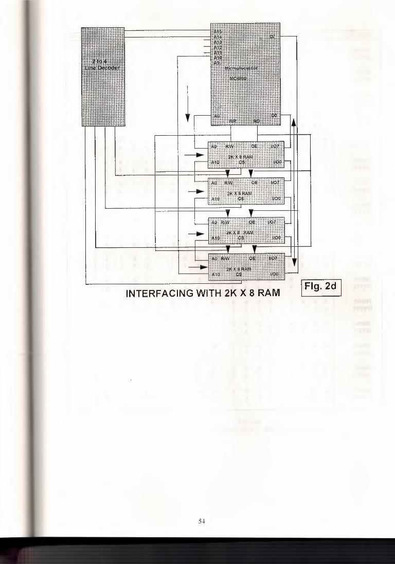
I Fig. 2d I INTERFACING WITH 2K X 8 RAM
54

ROM# Al5 Al4 Al3 A12 Al 1 AlO A9 A8 A7 A6 A5~A4 A3 A2 Al AO ADDRESS
0 0 0 0 0 0 0 0 0 0 0 0 0 0 0 0 OOOOH 0 0 0 0 {I 1 1 1 1 1 1 1 1 1 1 1 07FFH
0 0 0 0 1 0 0 0 0 0 0 0 0 0 0 0 0800H 0 0 0 0 1 1 1 1 1 1 1 1 1 1 1 1 OFFFH
0 0 0 1 (I 0 (I (I (I 0 0 (I (I 0 0 0 1000H (I 0 0 1 0 1 1 1 1 1 1 1 1 1 1 1 17FFH
0 0 0 1 1 0 0 0 (I 0 (I 0 0 0 0 0 1800H 0 0 0 1 1 1 1 1 1 1 1 1 1 1 1 1 lFFFH
1 0 (I 1 0 (I 0 (I 0 0 0 0 (I (I 0 0 0 2000H 0 0 1 0 0 1 1 1 1 1 1 1 1 1 1 1 27FFH
0 0 1 0 1 0 0 0 0 0 0 0 0 0 0 0 2800H 0 0 1 0 1 1 1 1 1 1 1 1 1 1 1 1 2FFFH
0 0 1 1 0 0 0 0 0 0 0 0 0 0 0 0 3000H 0 0 1 1 0 1 1 1 1 1 1 1 1 1 1 1 37FFH
0 0 1 1 1 0 0 0 (I (I (I (I (I 0 0 0 3800H 0 0 1 1 1 1 1 1 1 1 1 1 1 1 1 1 JFFFH
0 1 (I 0 (I 0 (I (I 0 0 (I (I 0 0 0 0 4000H 0 1 (I (I 0 1 1 1 1 1 1 1 1 1 1 1 47FFH
(I 1 0 0 1 0 (I () () 0 () 0 0 0 0 0 4800H 0 1 () 0 1 1 1 1 1 1 1 1 1 1 1 1 2FFFH
0 1 0 1 (I (I 0 0 0 0 0 0 0 0 0 0 5000H (I 1 (I 1 (I 1 1 1 1 1 1 1 1 1 1 1 57FFH
0 1 0 1 (I 0 (I 0 (I 0 0 0 0 0 0 0 5800H 0 1 0 1 1 1 1 1 1 1 1 1 1 1 1 1 SFFFH
2 0 1 1 0 0 0 0 0 (I 0 (I (I 0 0 0 0 6000H 0 1 1 0 (I 1 1 1 1 1 1 1 1 1 1 1 67FFH
(I 1 1 0 1 0 (I 0 0 0 (I 0 0 0 0 0 6800H 0 1 1 0 1 1 I 1 1 1 1 1 1 1 1 1 6FFFH
0 1 1 1 (I (I 0 0 0 0 0 0 0 0 0 0 7000H 0 1 1 1 0 1 1 1 1 1 1 1 1 1 1 1 77FFH
0 1 1 1 1 0 0 0 0 0 0 0 0 0 0 0 7800H 0 1 1 1 1 1 1 1 1 1 1 1 1 1 1 1 7FFFH
Table 2d NOTE : Eeach RAM contain 4K X 8 , and the total area is 64KB
Conti .
55

ROM Al5 A14 Al3 Al2 All AIO A9 A8 A7 A6 AS.A4 A3 A2 Al AO ADDRESS
#
1 0 0 0 0 0 0 0 0 0 0 0 0 0 0 0 8000H 1 0 0 0 0 1 1 1 1 1 1 1 1 1 1 1 87FFH
1 0 0 0 1 0 0 0 0 0 0 0 0 0 0 0 8800H 1 0 0 0 1 1 1 1 1 1 1 1 1 1 1 1 SFFFH
1 0 0 1 0 0 0 0 0 0 0 0 0 0 0 0 9000H 1 0 0 1 0 1 1 1 1 1 1 1 1 1 1 1 97FFH
1 0 0 1 1 0 0 0 0 0 0 0 0 0 0 0 9800H 1 0 0 1 1 1 1 1 1 1 1 1 1 1 1 1 9FFFH
3 1 0 1 0 0 0 0 0 0 0 0 0 0 0 0 0 AOOOH 1 0 1 () () 1 1 1 1 1 1 1 1 1 1 1 A7FFH
1 () 1 () 1 0 0 0 0 () 0 () 0 0 () 0 AS OOH 1 0 1 0 1 1 1 1 1 1 1 1 1 1 1 1 AFFFH
1 0 1 1 0 0 0 0 () 0 0 0 () 0 0 0 BOOOH 1 () 1 1 () 1 1 1 1 1 1 1 1 1 1 1 B7FFH
1 0 1 1 1 0 0 () 0 () 0 () 0 0 0 0 BS OOH 1 () 1 1 1 1 1 1 1 1 1 1 1 1 1 1 BFFFH
1 1 () 0 () 0 0 () 0 () 0 () 0 0 0 0 COOOH 1 1 0 0 0 1 1 1 1 1 1 1 1 1 1 1 C7FFH
1 1 0 0 1 0 0 () () 0 0 () 0 0 0 0 CSOOH 1 1 0 0 1 1 1 1 1 1 1 1 1 1 1 1 CFFFH
1 1 0 1 0 0 0 () 0 () 0 () 0 0 0 0 DOOOH 1 1 0 1 0 1 1 1 1 1 1 1 1 1 1 1 D7FFH
1 1 0 1 0 0 0 0 0 () 0 0 0 0 0 0 DSOOH 1 1 0 1 1 1 1 1 1 1 1 1 1 1 1 1 DFFFH
4 1 1 1 0 0 0 0 0 () () 0 0 0 0 0 0 EOOOH 1 1 1 0 0 1 1 1 1 1 1 1 1 1 1 1 E7FFH
-,;., 1 1 1 0 1 0 0 0 0 0 0 0 0 0 0 0 ES OOH 1 1 1 0 1 1 1 I 1 1 I 1 1 1 1 1 EFFFH
1 . 1 1 1 0 0 0 0 0 0 0 0 0 0 0 0 FOOOH 1 1 1 1 0 I 1 1 1 1 I 1 1 1 1 1 F7FFH
1 1 1 1 1 () 0 () 0 0 0 0 0 0 0 0 FSOOH 1 1 1 I 1 1 I I I 1 1 1 1 1 1 1 FFFFH
56

j Fig. 3a I INTERFACING WITH 4K X 8 RAM
ROM# Al5 Al4 Al 3 Al2 All AlO A9 A8 A7 A6 A5 A4 A3 A2 Al AO ADDRESS
1 0 0 0 0 0 0 0 0 0 0 0 0 0 0 0 0 0000 H 0 0 0 0 l 1 1 1 1 1 1 1 1 1 1 1 OFFFH
2 0 0 0 1 0 0 0 0 0 0 0 0 0 0 0 0 1000 H
0 0 0 1 1 1 1 1 1 1 1 1 1 1 1 1 lFFFH
3 0 0 1 0 0 0 0 0 0 0 0 0 0 0 0 0 2000 H
0 0 1 0 1 1 1 1 1 1 1 1 1 1 1 1 2FFFH
4 0 0 1 1 0 0 0 0 0 0 0 0 0 0 0 0 3000 H
0 0 1 1 1 1 1 1 1 1 1 1 1 1 1 1 3FFFH
Table 3a
NOTE : Eeach RAM contain 4K X 8, and the total area is 16KB
57

I Fig. 3b I INTERFACING WITH 4K X 8 RAM
58

ROM# Al5 Al4 Al3 Al2 All AJO A9 A8 A7 A6 A5~A4 A3 A2 Al AO ADDRESS
0 0 0 0 0 0 0 0 0 0 0 0 0 0 0 0 OOOOH 0 0 0 0 1 1 1 1 1 1 1 1 1 1 1 1 OFFFH
1 0 0 0 1 0 0 0 0 0 0 0 0 0 0 0 0 1000H 0 0 {I 1 1 1 1 1 1 1 1 1 1 1 1 1 lFFFH
{I 0 1 {I 0 0 0 0 0 0 {I 0 0 0 0 0 2000 H 0 0 1 0 1 1 1 1 1 1 1 1 1 1 1 1 2FFFH
2 0 0 1 1 0 0 0 0 0 {I 0 0 0 0 0 0 3000H 0 0 1 1 1 1 1 1 1 1 1 1 1 1 1 1 3FFFH
·o 1 0 0 0 0 0 0 0 0 0 0 0 0 0 0 4000H 0 1 0 0 1 1 1 1 1 1 1 1 1 1 1 1 4FFFH
3 0 1 0 1 0 0 0 0 0 0 0 0 0 0 0 0 SOOOH 0 1 0 1 1 1 1 1 1 1 1 1 1 1 1 1 SFFFH
0 1 1 0 1 0 0 0 0 0 0 0 0 0 0 0 6000H 0 1 1 0 1 0 1 1 1 1 1 1 1 1 1 1 6FFFH
4 0 1 1 l I I 0 0 0 0 0 0 0 0 0 0 7000H 0 1 I 1 1 l 1 1 1 1 1 1 1 1 1 1 7FFFH
Table 3b
NOTE : Ecach RAM contain 8K, and the total area is 32 KB
59

I Fig. 3c I
=
INTERFACING WITH 4K X 8 RAM
60

ROM# A15 A14 A13 A12 All AlO A9 A8 A7 A6 A5~A4 A3 A2 Al AO ADDRESS
0 0 0 0 0 0 () 0 0 0 0 0 0 0 0 0 OOOOH 0 0 0 0 1 1 1 1 1 1 1 1 1 1 1 1 OFFFH
0 () 0 1 () 0 0 0 () () () () () 0 0 0 1000H () 0 0 I I 1 I l 1 1 1 1 1 1 1 1 lFFFH
1 0 0 1 () 0 () () 0 0 0 0 0 0 0 0 0 2000H () () 1 0 I 1 1 1 I 1 1 1 1 1 1 1 2FFFH
0 () 1 1 () 0 () 0 () 0 0 () 0 0 0 0 3000H () 0 1 1 1 1 1 1 1 1 1 1 1 1 1 1 3FFFH
0 1 () 0 0 () 0 () 0 0 () () 0 0 0 0 4000H 0 1 () () 1 1 1 1 1 1 1 1 1 1 1 1 4FFFH
0 1 () 1 0 () 0 0 () () () 0 0 0 0 0 5000H 0 1 0 1 1 I 1 I 1 1 1 1 1 1 1 1 5FFFH
2 () 1 I 0 0 0 0 0 0 0 0 0 0 0 0 0 6000H () 1 1 0 1 I 1 1 1 I 1 1 1 1 1 1 6FFFH
0 1 1 1 0 0 0 0 0 0 0 0 0 0 0 0 7000H 0 1 1 1 1 1 1 1 1 1 1 1 1 1 1 1 7FFFH
1 0 0 0 0 0 0 0 0 0 0 0 0 0 0 0 8000H 1 0 0 () 1 1 I 1 1 1 1 1 1 1 1 1 8FFFH
1 0 0 1 0 () 0 0 0 0 () 0 0 0 0 0 9000H 1 0 0 1 1 1 1 1 1 1 1 1 1 1 1 1 9FFFH
3 1 0 1 0 0 0 0 0 0 0 0 0 0 0 0 0 AOOOH 1 0 1 0 1 1 1 1 1 I 1 1 1 1 1 1 AFFFH
1 0 1 1 0 0 0 0 0 0 0 0 0 0 0 0 BOOOH 1 0 1 1 1 1 1 1 1 I 1 1 1 1 1 1 BFFFH
1 1 0 0 0 0 0 0 0 0 0 0 0 0 0 0 COOOH 1 1 0 0 1 1 1 1 1 1 1 I 1 1 1 1 CFFFH
4' 1 1 0 1 0 0 0 0 0 0 () 0 0 () 0 0 DOOOH 1 1 () l 1 1 1 1 1 I 1 1 1 1 1 1 DFFFH
1 1 1 0 0 0 0 0 0 0 0 0 0 0 0 0 EOOOH 1 1 1 0 I I 1 I 1 1 1 1 1 1 1 1 EFFFH
1 1 1 1 0 0 0 0 0 0 0 0 0 0 0 0 FOOOH 1 1 1 1 1 1 1 1 I 1 1 1 1 1 1 1 FFFFH
Table 3c NOTE : Eeach RAM contain 16K , and the total area is 64 KB
61

I Fig. 4a I INTERFACING WITH 16K X 8 RAM
ROM# Al5 Al4 Al3 Al2 All AlO A9 AS A7 A6 A5 A4 A3 A2 Al AO ADDRESS 1 0 0 0 0 0 0 0 0 0 0 0 0 0 0 0 0 0000 H
0 0 1 1 1 1 1 1 1 1 1 1 1 1 1 1 JFFFH 2 0 1 0 0 0 0 0 0 0 0 0 0 0 0 0 0 4000 H
0 1 1 1 1 1 1 1 1 1 1 1 1 1 1 1 7FFFH . 3 1 0 0 0 0 0 0 0 0 0 0 0 0 0 0 0 8000 H
1 0 1 1 1 1 1 1 1 1 1 1 1 1 1 1 BFFFH 4 1 1 0 0 0 0 0 0 0 0 0 0 0 0 0 0 COOO H
1 1 1 1 1 1 1 1 1 1 1 1 1 1 1 1 FFFFH
Table 4a
NOTE: Ecach RAM contain 16K, and the total area is 64KB
62

Practical Conection
LA15 rv A14 A13 MICROPROCESSOR 07 A12 A11 06 A10 - A9 05 ~ AB A7 04 A6 A5 03 A4 A3 02 A2 A1
01 ,____
AO WR" RO 00 I--
r A7 vcc b....-+sv
r A6 AS h r A5 2KX8 A9 -, r A4 RAM W/R -, r A3 OE -, r A2 A10 ::J__ r A1 cs-, r AO 1/08 -,
~ 1/01 1/07 -, r 1/02 1/06 -, r 1/03 1/05 -,
GND 1/04 -,
- GND
r A7 vcc ::J._ r A6 AS -, +5V
r A5 2K X 8 A9-, r A4 RAM W/R -, r A3 OE h r A2 A10 b-- r A1 cs h r AO 1/08 h
L...r: 1/01 1/07 t-i r 1/02 1/06 h I r 1/03 1/05 h
~ GND l/04h Fig. Sa GND -
63

0
0 ORGATE
INVERTER

•
MEMORY DECODER ~
A15 A14 A13 A12 A11 A10
D7
Microptocessor
DO AO RD WR
I I R/W OE 1/07 A11
2K X 8 RAM 1/00 AO cs
A11 R/W OE 1/07
2K X 8 RAM 1/00 AO cs I I r-. 0 ORGATE
I Fig. Sc I 0 INVERTER
2K X 8 RAM
65

•
A1' A14 D7 A13 A12 A11 Microprocessor
MEMORY II MEMORY A10
DECODER DECODER
I I I WIR RD
.,, WR OE U01
2K X 8 RAM AO cs 1100
A11 WR OE U01
2K X 8 RAM AO cs 1100
A11 WR OE U01
2K X 8 RAM AO cs UCO
A11 WR OE U01
2K )(8 RAM AO cs 1100
A11 WR OE U01
2KX8RAM AO cs UCO
A11 WR OE U01
2K X 8 RAM AO cs UCO
A11 WR OE U01
2K XI RAM
INVERTER .. AO cs UCO
C)
0 ORGATE I I (\ I ~A11
WR OE U01
2KX8RAM
I Fig. 5c I AO cs UCO
66

•
APPENDIX II
67

~National ~ Semiconductor MM54HC32/MM74HC32 Quad 2-lnput OR Gate General Description These OR gates utilize advanced silicon-gate CMOS tech nology to achieve operating speeds similar to LS-TIL gates with the low power consumption of standard CMOS inte grated circuits. All gates have buffered outputs, providing high noise Immunity and the ability to dr:,e 10 LS- TIL loads. The 54HC/74HC logic family is functionally as well as pin out compatible with the standard 54LS/74LS logic family. All inputs are protected from damage due to static dis charge by internal diode clamps to Vee and ground.
Features • Typical propagation delay: 1 O ns • Wide power supply range: 2-6V • Low quiescent current: 20 µA maximum (74HC Series) • Low input currant: 1 µA maximum • Fanout of 10 LS-TIL loads
Connection and Logic Diagrams
Dual-In-Line Package
Vee B4 A4 Y4 B3 A3 Y3 '14 113 112 111 110 111 le
2 3 6
A1 B1 Y1
4 5 7
GND A2 B2 Y2 TL/F/5132-1
Top View
Order Number MM54HC32' or MM74HC32' • Please look inlo Section 8, Appendix D for availability of various package types.
Y=A+B y
TLIF/5132-2
(1 of 4)
A
B

Absolute Maximum Ratings (Notes 1 & 2) II Military/ Aerospace specified devices are required, contact the National Semiconductor Sales Office/ Olstrlbutors for avsllablllty and specifications. Supply Voltage (Vee) --0.5 to+ 7.0V
DC Input Voltage (V1N) -1.5 to Vee+ 1.5V pc Output Voltage (Vour) -0.5 to Vee+ 0.5V
3::: Operating Conditions 3:::
(J1
Min Max Units .l:o, ::i:
Supply Voltage iVec) 2 6 V (") w
DC Input or Output Voltage 0 Vee V I\.) .•.••... (V1N, Vour) s:
Operating Temp. Range (TA) s: MM74HC -40 + 85 'C
.....,
.l:o, MM54HC -55 + 125 'C :c
Input Rise or Fall Times (") w
(tr, t1) Vee=2.0V 1000 ns I\.)
Vee= 4.5V 500 ns Vcc=SOV 400 ns
Clamp Diode Current (11K, loK) DC Output Current, per pin (l~ur) DC Vee or GND Current, per pin (Ice) Storage Temperature Range (T sTG)
Power Dissipation (Po) (Note 3) S.O. Package only
Lead Temperature (h) (Soldering 10 seconds)
t 20 mA ±25 mA ±50mA
- 65'C to + 150'C
600mW 500mW
260'C
DC Electrical Characteristics (Note 4)
74HC I 54HC Symbol I Parameter I Conditions I Vee
TA= 25'C I TA= - 40 to 85'C TA= - 55 to 125'C I Units
Typ Guaranteed Limits
V1H I Minimum High Level 2.0V 1.5 1.5 1.5 V Input Voltage 4.5V 3.15 3.15 3.15 V
6.0V 4.2 4.2 4.2 V
V1L r Maximum Low Level 2.0V 0.5 0.5 0.5 V Input Voltaqe '" 4.5V 1.35 1.35 1.35 V
~- Minimum High Level
6.0V 1.8 1.8 1.8 V -
V1N = V1H or V1L Output Voltage l'ourl s: 20 µA I 2.0V 2.0 1.9 1.9 1.9
I V
4.5V 4.5 4.4 4.4 4.4 V 6.0V 6.0 5.9 5.9 5.9 V
V1N = V1H or V1L l'ourl s: 4.0 mA I 4.5V I 4. 7 I 3.98 I 3.84 I 3.7 I V l'ourl s: 5.2 mA 6.0V 5.2 5.48 5.34 5.2 V
Vol I Maximum Low Level V1N=V1L Output Voltaqs llourl s 20 µA j 2.0V 0 0.1 0.1 0.1
I V
4.5V 0 0.1 0.1 0.1 V 6.0V 0 0.1 0.1 0.1 V
I V1N=V1L l1ourls4.0mA 45V µ2 0.26 0.33
I 0.4
I V
1
llourl s 5.2 mA 6.0V 0.2 0.26 0.33 0.4 V B Maximum Input 6.0V ±0.1 ± 1.0 ± 1.0 µA V1N = Vee or GND I Current
Maximum Quiescent v1N=VccorGND I 6.ov I I 2.0 I 20 I 40 I µA Supply Current 'our= 0 µA ·----
Hote 1: Absolute Maximum Ratings are those values beyond which damage to the device may occur. Hoto 2: Unless othorwiso specified all voltages are •elerenced lo ground. llote 3: Pcwer Dissipation tempera lure derating - oiasuc '"N" package: - 12 mW/'C from 6'., C to 85'C: ceramic "J"" package: - 12 rn\"l!'C from 1 oo·c to 12s·c Hote 4: For a power supply ol SV ± 10% Iha worst case output voltages (VOH· and Vmi occur for HG al 4.5V. Thus lhe ,.sv v;,iuos should be used when designing with this supply. Worst case V1H and V1L occur at Vee- 5.5V and ,.sv respectively (Tho V1H vntuo al 5.SV is 3 85V.) The wor.s t case leakage current (11,i. 1cc, and 1oz) occur for CMOS at the higher voltage and so tho 6.0V values should be uso<J "V1L limits are currently tested at 20% of Vee- The above V1L specification (JQ"r'. ol Vee) will be ,mplernontod no later than 01. CY"89.

AC Electrical Characteristics vo.;=5V,TA=25·c.cL=15pF,tr=t,=sns
Guaranteed ~nits Limit
~=l:;um Propagation I_ I 10 I 1f1 _ns
Symbol Parameter I Conditions Typ
lrHL, tr1 H
AC Electrical Characteristics Vcc=2.0V to 6.0V, CL =50 pF, tr=t1=6 ns (unless otherwise specified)
Guaranteed Limits
125 150 25 30 21 25
95 110 19 22 16 19
- Units
- ns ns ns - ns ns ns - pF
- pF
Symbol I Parameter I I ~=25'C Conditions Yee Typ --
trHL, trLH I Maximum Propagation 2.0V 30 100
Delay 4.5V 12 20
I 6.0V 9 17
trLH, trnL I Maximum Output Rise --
2.0V 30 75 and Fall Time 4.5V 8 15
6.0V 7 13
Cpo I Power Dissipation I (per gate) I 50 Capacitance (Note 5)
C1N j Maximum Input I I I 5 r10 Capacitance
74HC I 54HC TA= -- 40 to 85°C TA= - 55 to 125'C
10 I 10
Nole 5: Cpo determines the no load dynamic power consurnptioo, Po-Cpo Vc,;;2, f + Ice Vee, and the no load dynamic current consumption. Is= Cpo Vee f + fee.

~National ~ Semiconductor MM54HC04/MM74HC04 Hex Inverter General Description These inverters utilize ,advanced silicon-gate CMOS tech nology to achieve operatlnq speeds slmitar to LS-TTL gates with the low power consumption of siandard CMOS inte grated circuits. The MM54HC04/MM74HC04 is a triple buffered inverter. It has high noise immunity and the ability to drive 1 O LS- TIL loads. The 54HC/7 4HC logic family is functionally as well as pin-out compatible with the standard 54LS/74LS logic fami ly. All inputs are protected from damage due to static dis charge by internal diode clamps to Vee and ground.
Features • Typical propagation delay: 8 ns • Fan out of 10 LS-TIL loads • Quiescent power consumption: 10 µW maximum at
room temperature • Low input current: 1 µA maximum
Connection and Logic Diagrams
Vee A6 Y8
Dual-In-Line Package
YS
13 12 10
AS A4 Y4
11 9 8
Al V1 A2
6
V2 Y3 GNO TL/F/5069-1
A3
Top View
Order Number MM54HC04' or MM74HC04' 'Please look into Section 8, Appendix D for availability of various package types
1 of 6 Inverters
TL/F/5069-2

Absolute Maximum Ratings (Notes 1 & 2) If MIiitary/Aerospace specltled devices are required, contact the National Semiconductor Sales Office/ Distributors for availability and specifications. Supply Voltage (Vee) ·-0.5 to + 7.0V
~ Operating Conditions ~
V, .t. Min Max Units :I:
Supply Voltage~(Vee) 2 6 V (")
2 DC Input or Output Voltage 0 Vee V ........•
(V1N, VouT) ~ ~
Operating Temp Range (T Al -...J MM74HC 40 + lJ5 oc .,;,.
::i: MM54HC .. 55 + 125 oc (")
0 Input Rise or Fall Times +>-
(tr, tf) Vee= z.ov 1000 ns Vee= 4.5V 500 ns Vcc=60V 400 ns
DC Input Voltage (V1N) DC Output Voltage (Vour) Clamp Diode Current (l1K, loKl DC Output Current, per pin (lclur) DC Vee or GND Current, per pin (1cc) Storage Temperature Range (TsrG) Power Dissipation (Po) (Nole 3) S.O. Package only
Lead Temperature (T Ll (Soldering 1 O seconds)
-1.5 to Vee+ 1.5V -0.5toVee+05V
.!:20 mA ± 25 mA ±50mA
- 65°C to + 150°C
600mW 500 mW
260°C
DC Electrical Characteristics (Note 4)
TA= 25'C 74HC 54HC
Symbol Parameter Conditions Vee TA= - 40 lo 85'C TA= -55 to 125'C Units
Typ Guaranteed Limits
V1H Minimum High Level 2.0V 1.5 1.5 1.5 V Input Voltage 4.5V 3.15 3.15 3.15 V
6.0V 4.2 4.2 4.2 V
V1L Maximum Low Level 2.0V 0.5 0.5 0.5 V lnpul Voltage'' 4.5V 1.35 1.35 1.35 V __ , __ 6.0V 1.8 1.8 1.8 V
VoH Minimum High Level V1N=Vfl Output Voltage l'our] s; 20 µA 2.0V 2.0 1.9 1.9 1.9 V
4.5V 4.5 4.4 4.4 4.4 V 6.0V 6.0 5.9 5.9 5.9 V
v,N= vfL . liourl s: 4.0 mA 4.5V 4.2 3.98 3.84 3.7 V
- l'ourl s; 5.2 mA 6.0V 5.7 5.48 5.34 5.2 V
Vol Maximum Low Level VtN=V1H Output Voltage I lour Is; 20 µA 2.0V 0 0.1 0.1 0.1 V
4.5V 0 0.1 0.1 0.1 V 6.0V 0 0.1 0.1 0.1 V
V1N=V1H I
l'ourl s;4.0 mA 4.5V 0.2 0.26 0.33 0.4 V -- l'ourl s; 5.2 mA 6.0V 0.2 0.26 0.33 0.4 V l1N Maximum Input V1N = Vee or GND 6.0V ±0.1 ± 1.0 ± 1.0 µA - Current
Maximum Quiescent V1N = Vee or GND 6.0V 2.0 20 40 µA Supply Current lour= o µA
Note 1: Absolute Maximum Ratings are those values beyond which damage to the device may occur.
Note 2: Unless otherwise specilied all vouaqcs are relerenced lo ground.
Note 3: Power Dissipation temperature derat,ng - plastic "N" package: - 12 mW/'C nom 65'e lo 85'C: ceramic "J'· package 12 mW/'e lrom 1oo·e lo 12s·e.
,iote 4: For a power supply ol SV ± 10% ihc worst case output voltages (VoH, and Ve,,) occur for HC al 4.5V Thus the 4.SV values should be used when designing ~'111 this supply. Worst case v,H and v1L occur at Vee= 5.5V and 4.5V respectively. i"r~e v1H value at 5.SV is 3 B5V.) The wor s: case leakage current (liN- Ice, and Oz/ occur for CMOS al the higher voltage and so the 6.0V values should be used.
"v,L limits are currently tosled al 20% of Vee- The above V1L specification (30% ol Vee) will be implomonted no later than 01. CY.89.

Absolute Maximum Ratings (Notes 1 & 2) Operating Conditions If Mllltary/ Aerospace specified devices are required, Min Max Units contact the National Semiconductor Sales Office/ Supply Voltage (Vee) 2 6 V Distributors for availability and specifications.
DC Input or Output Voltage 0 Vc;e V Supply Voltage (Vee) - 0.5 to + 7.0V
(V1N- Vou1l DC Input Voltage (V1N) -i.5toVee+1.5V
Operating Temp. Range (T Al DC Output Vnltage (VouT) -0.5 to Vee+O 5V
MM74HC -40 ! [15 oc Clamp Diode Current (l1K, loK) ±20 mA MM54HC -55 -I 125 'C DC Output Current, per pin (lbuT) ± 25 mA
Input Rise or Fall Times DC Vee or GND Current, per pin (lee) ±50 mA (tr, tr) Vee= 2 ov 1000 ns Storage Temperature Range (T sTG) -65'Cto +150'C Vee= 4 5V 500 ns Power Dissipation (Po) Vee= s.ov 400 ns
(Note 3) 600mW S.O. Package only 500 mW
Lead Temperature (h) (Soldering 1 O seconds) 260'C
DC Electrical Characteristics (Note 4)
TA=25'C 74HC 54HC
Symbol Parameter Conditions Vee TA= - 40 to 85'C TA=-55to125'C Units
Typ Guaranteed Limits
V1H Minimum High Level 2.0V 1.5 1.5 1.5 V Input Voltage 4.5V 3.15 3.15 3.15 V
6.0V 4.2 4.2 4.2 V
V1L Maximum Low Level 2.0V 0.5 0.5 0.5 V Input Voltage•' 4.5V 1.35 1.35 1.35 V
6.0V 1.8 1.8 1.8 V
VoH Minimum High Level V1N=V1t. Output Voltage l1ouTls20 µA 2.0V 2.0 1.9 1.9 1.9 V
4.5V 4.5 4.4 4.4 4.4 V 6.0V 6.0 5.9 5.9 5.9 V
V1N= V1L Jiourls4.0 mA 4.5V 4.2 3.98 3.84 3.7 V l'our] s 5.2 n1A 6.0V 5.7 5.48 5.34 5.2 V --
Vol Maximum low Level V1N=V1H Output Voltage l'oorl s20 µA 2.0V 0 0.1 0.1 0.1 V
4.5V 0 0.1 0.1 0.1 V 6.0V 0 0.1 0.1 0.1 V
V1N=V1H l'ourl s4.0 mA 4.5V 0.2 0.26 0.33 0.4 V liourls5.2 rnA 60V 0.2 0.26 0.33 0.4 V
l1N Maximum Input V1N = Vee or GND 6.0V ±0.1 ± 1.0 ± 10 u A
--- Current
Ice Maximum Quiescent V1N = Vee or GND 6.0V 2.0 20 40 µA
- Supply Current lour= o µA 14ot• 1: Absolute Maximum Ratings are lhoso values beyond which damage lo the dcvico may occur No10 2: Unless otherwise specified all vonaccs are referenced lo ground. Note J: Power Dissipation temperature dera1ong - plastic "N" package: - 12 mW/'C horn 65"C 10 85"C: ceramic "J" package 12 mW /"C from I OO'C lo 125'C. Nole 4: For a power supply of 5V 1 I 0% 11,e worst case output voltages (VoH, and Vr,,1.) occur for HC at 4.5V. Thus !ho 4.5V van.as should be used when designing ~ill\ lhls supply. worst case V1H and V11. occur at Vccc 5.SV and 4.5V respectively. (The V1H value al 5.SV is 3.85V.) The wor s: case leakage currenl (11N. 'cc. and oz) occur for CMOS al lhe higher vollage and so lhe 6.0V values should be used. ''V1L limils are currenlly lesled al 20% of Vee- The above V1L specificalion (30% of Vee) will be implomenled no laler than 01. cv·eg
·---·----~--------

AC Electrical Characteristics Vee= 5V, TA= 25'C, CL= 15 pF, t, = t, = 6 ns
Symbol Parameter Conditions Typ Guaranteed I Units Limit •
Maximum Propagation Delay '-----~~~-'--~~~~----~~-
8 15 ns
AC Electrical Characteristics Vee= 2.0V to 6.0V, CL= 50 pF, tr= tr= 6 ns (unless otherwise specified) -~ 1
T C 74HC 54HC =25' Symbol J Parameter J Conditions I Vee I A TA= - 40 to 85'C TA= -- 55 to 125'C I Units
Typ Guaranteed Limits tPHL, tPLH I Maximum Propagation -~.,·-2-.0-V--+-5-5--+ 95 120 145 ns -
Delay I . I 4.5V 11 19 24 29 ns 6.0V 9 16 20 24 ns - trLH, trHL / Maximum Output Rise I I 2.0V 30 75 95 110 ns
and Fall. Time 4.5V 8 15 19 22 ns 6.0V 7 13 16 19 ns
-- - Cp[) I Power Dissipation I (per gate) I 20 pF
Capacitance (Note 5)
C1N I Maxim~mlnput I I I 5 j 10 I 10 I 10 J pF Capacitance _ _
Hole 5: Cpo determines the no load dynamic power consumption.'P0-ep0 Vo::;2 f + Ice Vee, and the no load dynamic current consumption. 15 = Cpo Vee.I+ ice--_,

CX) (")
~ ~National ~ ~ Semiconductor ~ MM54HC138/MM74HC138 (") . u 3-to-8 Line Decoder ::x: ~ I General Descrip'tion :E This decoder utilizes advanced silicon-gate CMOS technol
ogy, and is well suited to memory address decoding or data routing applications. The circuit features high noise immuni ty and low power consumption usually associated with CMOS circuitry, yet has speeds comparable to low power Schottky TTL logic. The MM54HC138/MM74HC138 has 3 binary select inputs (A, B, and C). If the device is enabled these inputs deter mine which one of the eight normally higt1 outputs wilt go tow. Two active low and one active high enables (G1, G2A and 028) are provided to ease the cascading of decoders.
The decoder's outputs can drive 10 tow power Schottky TTL equivalent loads, and are functionally and pin equivalent to the 54LS138/7 4LS 138. All inputs are protected from dam age due to static discharge by diodes to Vee and ground.
Features • Typical propagation delay: 20 ns • Wide power supply range: 2V-6V • Low quiescent current: 80 µA maximum (74HC Series) • Low input current: 1 µA maximum • Fanout of 10 LS-TTL loads
Connection and Logic Diagrams
DATA OUTPUTS
15 <r-YO Dual-In-Line Package
Vee YO YI Y2 YJ YI Y5 Y6
TL/F/5120-2
Inputs Outputs Enable Select
G1 02· C B A YO Y1 Y2 Y3 Y4 Y5 Y6 Y7
X H X X X H H H H H H H H
L X X X X H H H H H H H H
H L L L L L H H H H H H H
H L L L H H L H H H H H H
H L L H L H H L H H H H 1-1 H L L H H 1-1 H H L H H H H
H L H L L H H H H L H H H
H L H L H H H H H H L H H
H L H H L H H H 1-1 1-1 H L H
H L H H H H H H H H H H L
3-108
,_b_~14 13 12 11 10 s
\ I ' 1\ I
- o-
' 0
1 2 3 • 5 B 7 18
A
Irr~ nfB 01 Y7 OHO m~ OUTPUT ffi
SELECT EH ABLE
TOP VIEW TL/F/5120··•
Order Number MM54HC138• or MM74HC138* 01 L..../
'Please look inlo Section 6, Appendix D for availability of various package types.
Truth Table
'G2= G2A+G28 H = high level, L = low level, X = don't care

Absolute Maximum Ratings (Notes 1 & 2) If MIiitary I Aerospace specified devices are required, contact the National Semiconductor Sales Office/ Distributors for avallablllty and specifications. · Supply Voltage (Vee) -0.5 to+ 7.0V DC Input Voltage (ViN) -1.5 to Vee+ 1.5V DC Output Voltage (Vourl -0.5 to Vee+ 0.5V Clamp Diode Current (liK, Im<) ± 20 mA DC Output Current, per pin (lour) ± 25 mA DC Vee or GND Current, per pin (Ice) ± 50 mA Storage Temperature Range (T sro) - 65'C to + 150'C Power Dissipation (Po) (Note 3) S.O. Package only
600mW 500mW
Lead Temp. (TL) (Soldering 10 seconds) 260'C
Operating Conditions Min 2 Supply Voltage (Vee)
DC Input ~r Output Voltage (V1N, Vourl
Operating Temp. Range (T Al MM74HC MM54HC
Max 6
Vee
Units V V 0
-40 -55
+85 + 125
'C 'C
Input Rise or Fall Times (t,. t1) Vee"' z.ov
Vee~ 4.5V Vee= s.ov
1000 500 400
ns ns ns
Symbol
DC Electrical Characteristics (Note 4)
Parameter Conditions Vee 74HC 54HC
TA= - 55 to 125'C I Units
Guaranteed Limits ---~--·~ 1.5 1.5 1.5 V 3.15 3.15 3.15 V 4.2 4.2 4.2 V
0.5 0.5 0.5 V 1.35 1.35 1.35 V 1.8 1.8 1.8 V
Typ
VoH
Minimum High Level Input Voltage
2.0V 4.5V 6.0V
Maximum Low Level Input Voltage••
2.0V 4.5V 6.0V
2.0 4.5 6.0
1.9 4.4 5.9
1.9 4.4 5.9
1.9 4.4 5.9
V V V
Minimum High Level Output Voltage
V1N = V1H or V1L \ 'curl s 20 µA 2.0V
4.5V 6.0V
V1N = V1H or V1L \lour\ s4.0 mA \lour\s5.2 mA
4.5V 6.0V
4.2 5.7
3.98 5.48
3.84 5.34
3.7 5.2
V V
Maximum Low Level Output Voltage
V1N = V1H or V1L \lour\s20 µA 0
0 0
0.1 0.1 0.1
2.0V 4.5V
I--------+· 6.0V \ v \ v , \ ~-. \
0.1 0.1 0.1
0.1 0.1 0.1
V V V
VtN = V1H or V11_ \lour\s4.0 mA \lour\ s 5.2 mA
4.5V 6.0V
Maximum Input Current
v,N=Vcc or GND I 6.0V
0.2 0.2
0.26 0.26
0.33 0.33
0.4 0.4
V V
±0.1
Ice
± 1.0 ± 1.0 µA
Maximum Quiescent . Supply Current
V1N=Vec or GND lour=O µA
6.0V 80 160 µA 8.0
Note 1: Absolute Maximum Ratings are those values beyond which damage to the device may occur.
Note 2.: Unless otherwise specified all voltages are referenced to ground. Note 3: Power Dissipation temperature derating - plastic "N" package: - 12 mW /'C from 65'C to 85'C; ceramic "J" package: - 12 mW /'C from 1 OO'C lo 125'C. Note 4: For a power supply of 5V ± 10% the worst case output voltages (VoH, and VOL) occur ior HC al 4.5V. Thus the 4.5V values should be used when designing with this supply. Worst case v,H and v,L occur at Vee= 5.5V and 4.5V respectively. (The v1H value al 5.5V is 3.85V.) The worst case leakage current (l1N, Ice, and 'ozl occur for CMOS al the higher voltage and so the 6.0V values should be used. "V1L limits are currently tested at 20% of Vee, The above V1L specification (30% of Vee) will be implemented no later than 01, CY'69.
3-109
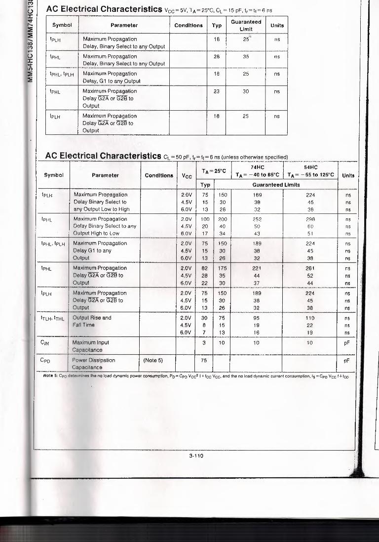
AC Electrical Characteristics Vee= 5V, TA= 25°C, CL= 15 pF, Ir= t, = 6 ns ~·
Symbol Parameter Conditions Typ Guaranteed
Units Limit -·.
trLH Maximum Propagation 18 25• ns Delay, Binary Select to any Output
trHL Maximum Propagation 28 35 ns Delay, Binary Select to any Output
trHL, trLH Maximum Propagation 18 25 ns Delay, G1 to anyOutput
trHL Maximum Propagation 23 30 ns Delay G2A or G2B to Output
tpLH Maximum Propagation 18 25 ns Delay G2A or G2B to Output
" .
~-c Electrical Characteristics CL= 50 pF, tr= tr= 6 ns (unless otherwise specified) TA=25'C
74HC 54HC Symbol Parameter Conditions Vee TA= - 40 to 85'C TA= - 55 to 125'C Units
Typ Guaranteed Limits
IPLH Maximum Propagation 2.0V 75 150 189 224 ns Qelay Binary Select to 4.5V 15 30 38 45 ns any Output Low to High 6.0V 13 26 32 38 ns
tPHL Maximum Propagation 2.0V 100 200 252 298 ns Delay Binary Select to any 4.5V 20 40 50 60 ns
' Output High to Low 6.0V 17 34 43 51 ns
tPHL, trLH Maximum Propagation 2.0V 75 150 189 224 ns Delay G 1 to any 4.5V 15 30 38 45 ns Output 6.0V 13 26 32 38 ns
trHL Maximum Propagation 2.0V 82 175 221 261 ns Delay G2A or G2B to 4.5V 28 35 44 52 ns Output 6.0V 22 30 37 44 ns
tru-i Maximum Propagation 2.0V 75 150 189 224 ns Delay G2A or G2B to 4.5V 15 30 38 45 ns Output 6.0V 13 26 32 38 ns -
trLH, trHL Output Rise and 2.0V 30 75 95 110 ,.
ns Fall Time 4.5V 8 15 19 22 ns
6.0V 7 13 16 19 ns :
C1N Maximum Input 3 10 10 10 pF l;
Capacitance
Cpo Power Dissipation (Note 5) 75 pF Capacitance
Note 5: Cpo determines the no load dynamic power consumptlon, Po= Cpo Vcc2 f +· Ice Vee, and the no load dynamic current consumption, Is= Cpo Vee f + ice.
· ... 3.110

References
2. :\Iicrocompott"r
68