ncp1288 - controller, fixed frequency, current mode, for
TRANSCRIPT

© Semiconductor Components Industries, LLC, 2011
July, 2011 − Rev. 31 Publication Order Number:
NCP1288/D
NCP1288
Controller, Fixed Frequency, Current Mode, for Flyback Converters
The NCP1288 is a new generation of the NCP12xx fixed−frequency current−mode controllers featuring a high−voltage startup current, pin−to−pin compatible with the previous generation.
Due to its proprietary Soft−Skip™ mode combined with frequency foldback, the controller exhibits excellent efficiency in light load condition while still achieving very low standby power consumption. This Soft−Skip feature also dramatically reduces the risk of acoustic noise, which enables the use of inexpensive transformers and capacitors in the clamping network.
Internal frequency jittering, ramp compensation, and a versatile latch input make this controller an excellent candidate for converters where ruggedness and components cost are the key constraints.
In addition, the controller includes a new high voltage circuitry that combines a startup current source and a brown−out / line OVP detector able to sense the input voltage either from the rectified ac line or the dc filtered bulk voltage.
Finally, due to a careful design, the precision of critical parameters is well controlled over the entire temperature range (−40°C to+125°C), enabling easier design and increased safety (e.g. �5% forthe peak current limit, �7% for the oscillator).
Features
• Timer−Based Overload Protections with Auto−Recovery (Option B) or Latched (Option A) Operation
• High−Voltage Current Source with Built−in Brown−outand Line Overvoltage Protections
• Fixed−Frequency Current−Mode Operation withBuilt−in Ramp Compensation
• Frequency Jittering for a Reduced EMI Signature
• Adjustable Overpower Compensation
• Latch−off Input for Severe Fault Conditions, withDirect Connection of an NTC for OvertemperatureProtection (OTP)
• Protection Against Winding Short−Circuit
• Frequency Foldback transitioning into Soft−Skip forImproved Performance in Standby
• 65 kHz Oscillator (100 kHz and 133 kHz VersionsAvailable Upon Request)
• VCC Operation up to 28 V
• Increased Precision on Critical Parameters
• ±1.0 A Peak Drive Capability
• 4.0 ms Soft−Start
• Internal Thermal Shutdown with Hysteresis
• These Devices are Pb−Free, Halogen Free/BFR Freeand are RoHS Compliant*
Typical Applications• ac−dc Adapters for Notebooks, LCD, and Printers
• Offline Battery Chargers
• Consumer Electronic Power Supplies
• Auxiliary/Housekeeping Power Supplies
*For additional information on our Pb−Free strategy and soldering details, pleasedownload the ON Semiconductor Soldering and Mounting TechniquesReference Manual, SOLDERRM/D.
SOIC−7CASE 751U
MARKINGDIAGRAM
http://onsemi.com
88XffALYWX
�
1
8
88Xff = Specific Device CodeX = A or Bff = 65, 00, or 33
A = Assembly LocationL = Wafer LotY = YearW = Work Week� = Pb−Free Package
See detailed ordering and shipping information in the packagedimensions section on page 38 of this data sheet.
ORDERING INFORMATION
NCP1288
http://onsemi.com2
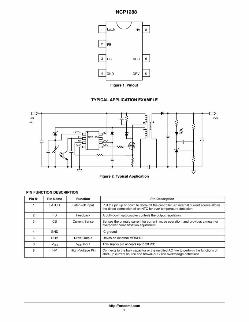
1
2
3
4
8
6
5
Latch
FB
CS
GND
HV
VCC
DRV
Figure 1. Pinout
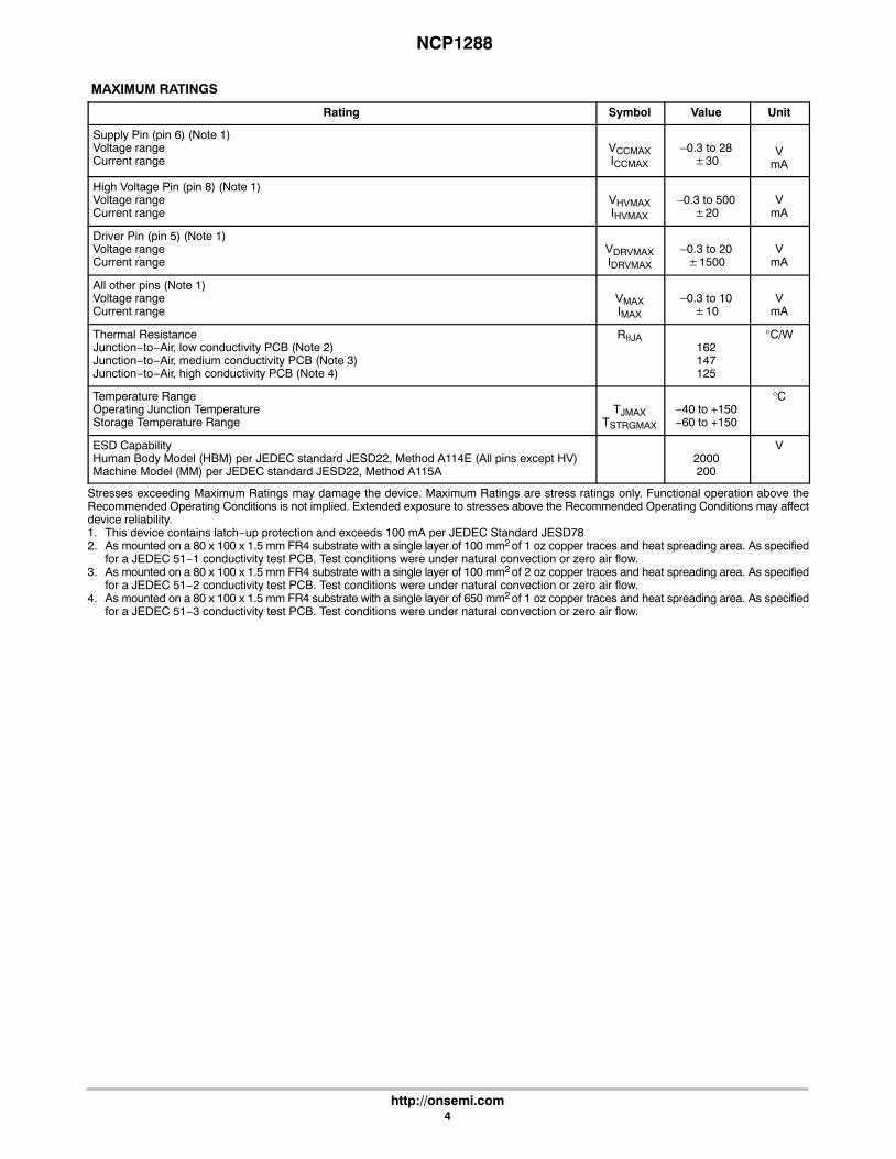
TYPICAL APPLICATION EXAMPLE
VOUTVIN
(dc)
NCP1288
LATCH
FB
CS
GND
HV
VCC
DRV
Figure 2. Typical Application
PIN FUNCTION DESCRIPTION
Pin N� Pin Name Function Pin Description
1 LATCH Latch−off Input Pull the pin up or down to latch−off the controller. An internal current source allowsthe direct connection of an NTC for over temperature detection
2 FB Feedback A pull−down optocoupler controls the output regulation.
3 CS Current Sense Senses the primary current for current−mode operation, and provides a mean foroverpower compensation adjustment.
4 GND – IC ground
5 DRV Drive Output Drives an external MOSFET
6 VCC VCC Input This supply pin accepts up to 28 Vdc
8 HV High−Voltage Pin Connects to the bulk capacitor or the rectified AC line to perform the functions ofstart−up current source and brown−out / line overvoltage detections

NCP1288
http://onsemi.com3
SIMPLIFIED INTERNAL BLOCK SCHEMATIC
Figure 3. Simplified Internal Block Schematic
Reset
Brown−out
CS
FB
−+
blanking
timer
VDD
−+
−+
+−
+
+
S
RQ
Soft−start Start
Reset
IC Start
IC Stop
Oscillator
HV
VCC
Latch
−+
+
Vskip
ProtectionMode
release
timer
Autorecoveryprotectionmode only
DRV
HV sample
OVM
BO
Clamp
UVLO
Fault
Reset
Sawtooth
Jitter
HV stop
Brown−out
HV stop −+
V to I
HV sample
−+
+
Latch
Dual HVstart−upcurrent source
VCCmanagement
HV currentTSD
VDDUVLOReset
TSD
StartIC Start
Skip
PWM
Soft−start
Reset
VDDUVLO
Soft−skip ramp
IC stop
TSD
TSD
HV dc
PWM
Fault Flag
Foldback
FB
GND
FB
Stop
Skip
S
RQ
blanking
−+
S
RQ
−+
blanking
Brown−out
Reset
Latch
Vclamp
blanking
1 k�+
+
Soft−startend
Soft−start end
End
slopecomp.
ramp
IOPC = 0.5� x(VHV−125)
VDD
INTC
INTC VOVP
VOTP
tLatch(OVP)
tLatch(OTP)
tSSKIP
RFB(up)
KFB
ILIMIT
DMAX
tSSTART
VFB(OPC)
tLEB
tBCSVILIM ILIMIT
VCS(stop)
DCMAX
DMAX
tfault tautorec
NCP1288
http://onsemi.com4
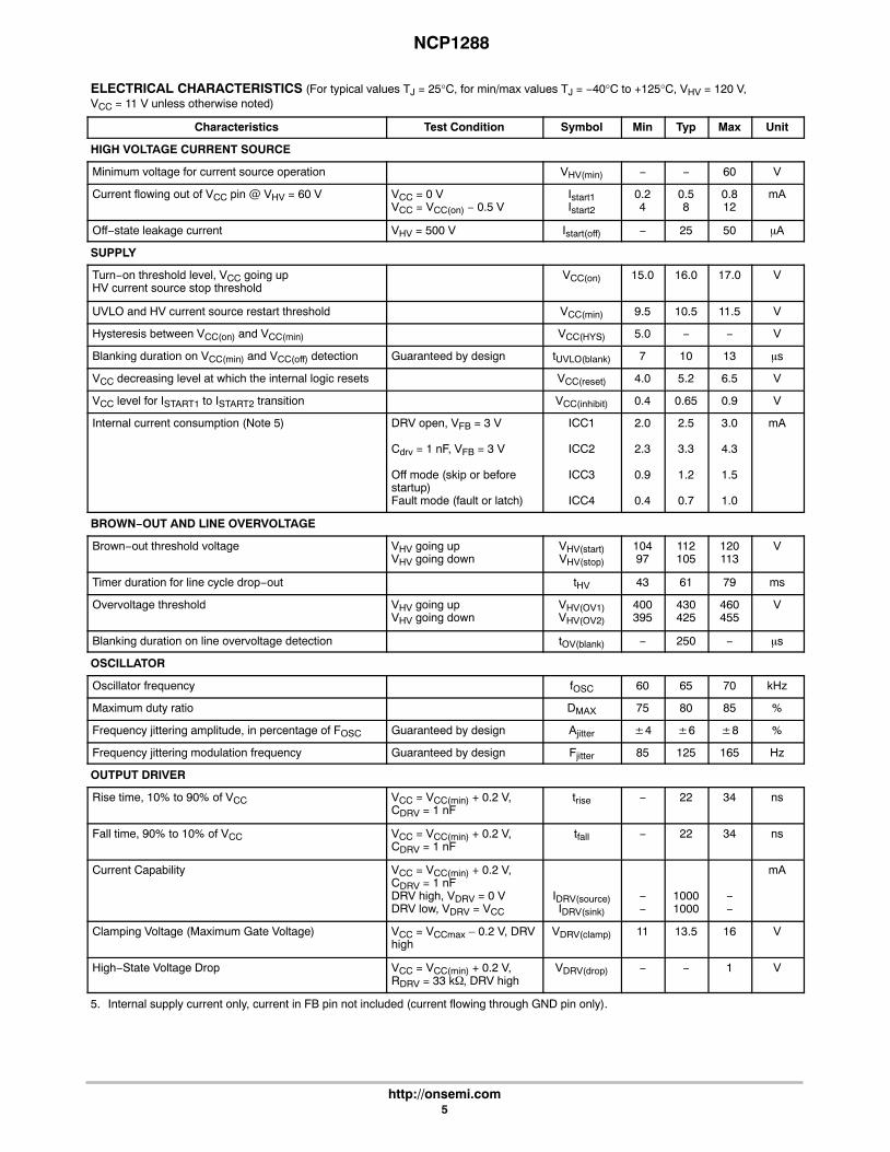
MAXIMUM RATINGS
Rating Symbol Value Unit
Supply Pin (pin 6) (Note 1)Voltage rangeCurrent range
VCCMAXICCMAX
–0.3 to 28�30
VmA
High Voltage Pin (pin 8) (Note 1)Voltage rangeCurrent range
VHVMAXIHVMAX
–0.3 to 500�20
VmA
Driver Pin (pin 5) (Note 1)Voltage rangeCurrent range
VDRVMAXIDRVMAX
–0.3 to 20�1500
VmA
All other pins (Note 1)Voltage rangeCurrent range
VMAXIMAX
–0.3 to 10�10
VmA
Thermal ResistanceJunction−to−Air, low conductivity PCB (Note 2)Junction−to−Air, medium conductivity PCB (Note 3)Junction−to−Air, high conductivity PCB (Note 4)
R�JA162147125
°C/W
Temperature RangeOperating Junction TemperatureStorage Temperature Range
TJMAXTSTRGMAX
−40 to +150−60 to +150
°C
ESD CapabilityHuman Body Model (HBM) per JEDEC standard JESD22, Method A114E (All pins except HV)Machine Model (MM) per JEDEC standard JESD22, Method A115A
2000200
V
Stresses exceeding Maximum Ratings may damage the device. Maximum Ratings are stress ratings only. Functional operation above theRecommended Operating Conditions is not implied. Extended exposure to stresses above the Recommended Operating Conditions may affectdevice reliability.1. This device contains latch−up protection and exceeds 100 mA per JEDEC Standard JESD782. As mounted on a 80 x 100 x 1.5 mm FR4 substrate with a single layer of 100 mm2 of 1 oz copper traces and heat spreading area. As specified
for a JEDEC 51−1 conductivity test PCB. Test conditions were under natural convection or zero air flow.3. As mounted on a 80 x 100 x 1.5 mm FR4 substrate with a single layer of 100 mm2 of 2 oz copper traces and heat spreading area. As specified
for a JEDEC 51−2 conductivity test PCB. Test conditions were under natural convection or zero air flow.4. As mounted on a 80 x 100 x 1.5 mm FR4 substrate with a single layer of 650 mm2 of 1 oz copper traces and heat spreading area. As specified
for a JEDEC 51−3 conductivity test PCB. Test conditions were under natural convection or zero air flow.
NCP1288
http://onsemi.com5
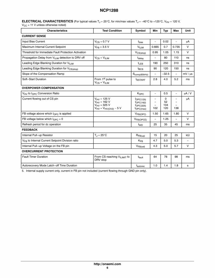
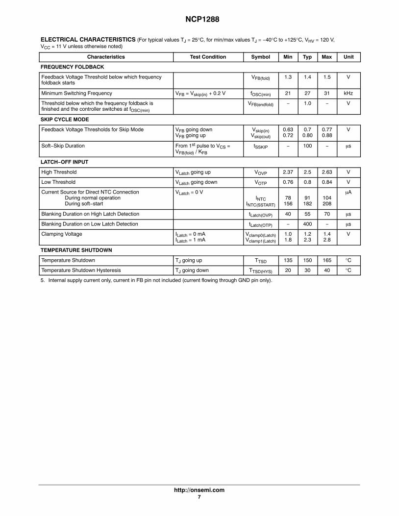
ELECTRICAL CHARACTERISTICS (For typical values TJ = 25°C, for min/max values TJ = −40°C to +125°C, VHV = 120 V, VCC = 11 V unless otherwise noted)
Characteristics Test Condition Symbol Min Typ Max Unit
HIGH VOLTAGE CURRENT SOURCE
Minimum voltage for current source operation VHV(min) − − 60 V
Current flowing out of VCC pin @ VHV = 60 V VCC = 0 VVCC = VCC(on) − 0.5 V
Istart1Istart2
0.24
0.58
0.812
mA
Off−state leakage current VHV = 500 V Istart(off) − 25 50 �A
SUPPLY
Turn−on threshold level, VCC going upHV current source stop threshold
VCC(on) 15.0 16.0 17.0 V
UVLO and HV current source restart threshold VCC(min) 9.5 10.5 11.5 V
Hysteresis between VCC(on) and VCC(min) VCC(HYS) 5.0 − − V
Blanking duration on VCC(min) and VCC(off) detection Guaranteed by design tUVLO(blank) 7 10 13 �s
VCC decreasing level at which the internal logic resets VCC(reset) 4.0 5.2 6.5 V
VCC level for ISTART1 to ISTART2 transition VCC(inhibit) 0.4 0.65 0.9 V
Internal current consumption (Note 5) DRV open, VFB = 3 V
Cdrv = 1 nF, VFB = 3 V
Off mode (skip or beforestartup)Fault mode (fault or latch)
ICC1
ICC2
ICC3
ICC4
2.0
2.3
0.9
0.4
2.5
3.3
1.2
0.7
3.0
4.3
1.5
1.0
mA
BROWN−OUT AND LINE OVERVOLTAGE
Brown−out threshold voltage VHV going upVHV going down
VHV(start)VHV(stop)
10497
112105
120113
V
Timer duration for line cycle drop−out tHV 43 61 79 ms
Overvoltage threshold VHV going upVHV going down
VHV(OV1)VHV(OV2)
400395
430425
460455
V
Blanking duration on line overvoltage detection tOV(blank) − 250 − �s
OSCILLATOR
Oscillator frequency fOSC 60 65 70 kHz
Maximum duty ratio DMAX 75 80 85 %
Frequency jittering amplitude, in percentage of FOSC Guaranteed by design Ajitter �4 �6 �8 %
Frequency jittering modulation frequency Guaranteed by design Fjitter 85 125 165 Hz
OUTPUT DRIVER
Rise time, 10% to 90% of VCC VCC = VCC(min) + 0.2 V,CDRV = 1 nF
trise − 22 34 ns
Fall time, 90% to 10% of VCC VCC = VCC(min) + 0.2 V,CDRV = 1 nF
tfall − 22 34 ns
Current Capability VCC = VCC(min) + 0.2 V,CDRV = 1 nFDRV high, VDRV = 0 VDRV low, VDRV = VCC
IDRV(source)IDRV(sink)
−−
10001000
−−
mA
Clamping Voltage (Maximum Gate Voltage) VCC = VCCmax – 0.2 V, DRVhigh
VDRV(clamp) 11 13.5 16 V
High−State Voltage Drop VCC = VCC(min) + 0.2 V,RDRV = 33 k�, DRV high
VDRV(drop) − − 1 V
5. Internal supply current only, current in FB pin not included (current flowing through GND pin only).
NCP1288
http://onsemi.com6
ELECTRICAL CHARACTERISTICS (For typical values TJ = 25°C, for min/max values TJ = −40°C to +125°C, VHV = 120 V, VCC = 11 V unless otherwise noted)
Characteristics UnitMaxTypMinSymbolTest Condition
CURRENT SENSE
Input Bias Current VCS = 0.7 V Ibias − 0.02 − �A
Maximum Internal Current Setpoint VFB > 3.5 V VILIM 0.665 0.7 0.735 V
Threshold for Immediate Fault Protection Activation VCS(stop) 0.95 1.05 1.15 V
Propagation Delay from VILIM detection to DRV off VCS = VILIM tdelay − 80 110 ns
Leading Edge Blanking Duration for VILIM tLEB 190 250 310 ns
Leading Edge Blanking Duration for VCS(stop) tBCS 90 120 150 ns
Slope of the Compensation Ramp Scomp(65kHz) − −32.5 − mV / �s
Soft−Start Duration From 1st pulse to VCS = VILIM
tSSTART 2.8 4.0 5.2 ms
OVERPOWER COMPENSATION
VHV to IOPC Conversion Ratio KOPC − 0.5 − �A / V
Current flowing out of CS pin VHV = 125 VVHV = 162 VVHV = 325 VVHV = VHV(OV2) − 5 V
IOPC(125)IOPC(162)IOPC(325)IOPC(max)
−−−
102
052104120
−−−
138
�A
FB voltage above which IOPC is applied VFB(OPC) 1.50 1.65 1.80 V
FB voltage below which IOPC = 0 VFB(OPCE) − 1.25 − V
Refresh period for dc operation tWD 25 35 45 ms
FEEDBACK
Internal Pull−up Resistor TJ = 25°C RFB(up) 15 20 25 k�
VFB to Internal Current Setpoint Division ratio KFB 4.7 5.0 5.3 −
Internal Pull−up Voltage on the FB pin VFB(ref) 4.3 5.0 5.7 V
OVERCURRENT PROTECTION
Fault Timer Duration From CS reaching VILIMIT toDRV stop
tfault 64 78 98 ms
Autorecovery Mode Latch−off Time Duration tautorec 1.0 1.4 1.8 s
5. Internal supply current only, current in FB pin not included (current flowing through GND pin only).
NCP1288
http://onsemi.com7
ELECTRICAL CHARACTERISTICS (For typical values TJ = 25°C, for min/max values TJ = −40°C to +125°C, VHV = 120 V, VCC = 11 V unless otherwise noted)
Characteristics UnitMaxTypMinSymbolTest Condition
FREQUENCY FOLDBACK
Feedback Voltage Threshold below which frequencyfoldback starts
VFB(fold) 1.3 1.4 1.5 V
Minimum Switching Frequency VFB = Vskip(in) + 0.2 V fOSC(min) 21 27 31 kHz
Threshold below which the frequency foldback isfinished and the controller switches at fOSC(min)
VFB(endfold) − 1.0 − V
SKIP CYCLE MODE
Feedback Voltage Thresholds for Skip Mode VFB going downVFB going up
Vskip(in)Vskip(out)
0.630.72
0.70.80
0.770.88
V
Soft−Skip Duration From 1st pulse to VCS =VFB(fold) / KFB
tSSKIP − 100 − �s
LATCH−OFF INPUT
High Threshold VLatch going up VOVP 2.37 2.5 2.63 V
Low Threshold VLatch going down VOTP 0.76 0.8 0.84 V
Current Source for Direct NTC ConnectionDuring normal operationDuring soft−start
VLatch = 0 VINTC
INTC(SSTART)
78156
91182
104208
�A
Blanking Duration on High Latch Detection tLatch(OVP) 40 55 70 �s
Blanking Duration on Low Latch Detection tLatch(OTP) − 400 − �s
Clamping Voltage ILatch = 0 mAILatch = 1 mA
Vclamp0(Latch)Vclamp1(Latch)
1.01.8
1.22.3
1.42.8
V
TEMPERATURE SHUTDOWN
Temperature Shutdown TJ going up TTSD 135 150 165 °C
Temperature Shutdown Hysteresis TJ going down TTSD(HYS) 20 30 40 °C
5. Internal supply current only, current in FB pin not included (current flowing through GND pin only).
NCP1288
http://onsemi.com8
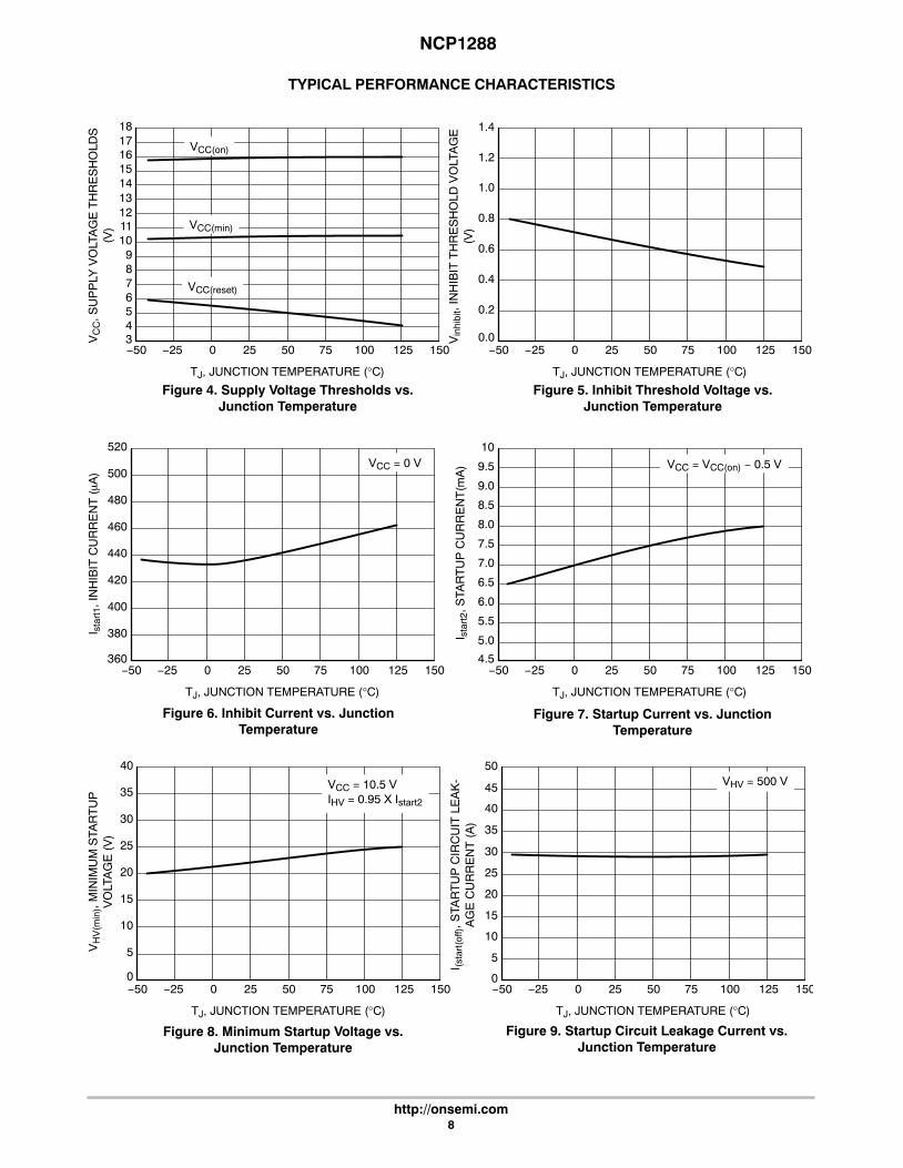
TYPICAL PERFORMANCE CHARACTERISTICS
TJ, JUNCTION TEMPERATURE (°C)
150125100250−503
5
7
9
11
VC
C, S
UP
PLY
VO
LTA
GE
TH
RE
SH
OLD
S(V
)
Figure 4. Supply Voltage Thresholds vs.Junction Temperature
Figure 5. Inhibit Threshold Voltage vs.Junction Temperature
Figure 6. Inhibit Current vs. JunctionTemperature
Figure 7. Startup Current vs. JunctionTemperature
Figure 8. Minimum Startup Voltage vs.Junction Temperature
7550−25
TJ, JUNCTION TEMPERATURE (°C)
150125100250−500.0
0.2
0.4
0.6
1.0
Vin
hibi
t, IN
HIB
IT T
HR
ES
HO
LD V
OLT
AG
E(V
)
7550−25
4
6
8
10
1213
TJ, JUNCTION TEMPERATURE (°C)
150125100250−50360
400
440
480
520
I sta
rt1,
INH
IBIT
CU
RR
EN
T (�A
)
7550−25
0.8
380
420
460
500
TJ, JUNCTION TEMPERATURE (°C)
150125100250−504.5
5.5
6.5
7.5
I sta
rt2,
STA
RT
UP
CU
RR
EN
T(m
A)
7550−25
5.0
6.0
7.0
8.0
TJ, JUNCTION TEMPERATURE (°C)
150125100250−500
5
10
15
30
VH
V(m
in),
MIN
IMU
M S
TAR
TU
PV
OLT
AG
E (
V)
7550−25
20
25
TJ, JUNCTION TEMPERATURE (°C)
150125100250−500
10
20
30
40
I (sta
rt(o
ff), S
TAR
TU
P C
IRC
UIT
LE
AK
-A
GE
CU
RR
EN
T (
A)
7550−25
5
15
25
35
45
50
VCC(reset)
VCC(min)
VCC(on)
1.4
1.2
VCC = 0 V VCC = VCC(on) − 0.5 V
8.5
9.5
9.0
10
40
35VCC = 10.5 VIHV = 0.95 X Istart2
VHV = 500 V
Figure 9. Startup Circuit Leakage Current vs.Junction Temperature
14
1615
1718
NCP1288
http://onsemi.com9
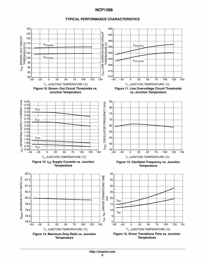
TYPICAL PERFORMANCE CHARACTERISTICS
TJ, JUNCTION TEMPERATURE (°C)
150125100250−5080
90
100
110
120
VH
V, B
RO
WN−
OU
T C
IRC
UIT
TH
RE
SH
OLD
S (
V)
Figure 10. Brown−Out Circuit Thresholds vs.Junction Temperature
Figure 11. Line Overvoltage Circuit Thresholdsvs. Junction Temperature
Figure 12. ICC Supply Currents vs. JunctionTemperature
Figure 13. Oscillator Frequency vs. JunctionTemperature
Figure 14. Maximum Duty Ratio vs. JunctionTemperature
7550−25
TJ, JUNCTION TEMPERATURE (°C)
150125100250−50410
415
420
425
435
VH
V, L
INE
OV
ER
VO
LTA
GE
CIR
CU
ITT
HR
ES
HO
LDS
(V
)
7550−25
85
95
105
115
125
130
TJ, JUNCTION TEMPERATURE (°C)
150125100250−500.50
1.00
1.50
2.00
2.50
I CC
, OP
ER
AT
ING
SU
PP
LY C
UR
RE
NT
(m
A)
7550−25
430
0.75
1.25
1.75
2.25
TJ, JUNCTION TEMPERATURE (°C)
150125100250−5045
55
65
75
f OS
C, O
SC
ILLA
TO
R F
RE
QU
EN
CY
(kH
z)
7550−25
50
60
70
80
TJ, JUNCTION TEMPERATURE (°C)
150125100250−5078.0
78.5
79.0
79.5
81.0
DM
AX, M
AX
IMU
M D
UT
Y R
AT
IO (
%)
7550−25
80.0
80.5
TJ, JUNCTION TEMPERATURE (°C)
150125100250−500
10
20
30
40
t rise
, tfa
ll, D
RIV
ER
TR
AN
SIT
ION
S T
IME
(ns)
7550−25
5
15
25
35
VHV(start)
450
440
ICC1
85
82.0
81.5
tfall
VHV(stop)
445
VHV(OV1)
VHV(OV2)
2.75
3.25
3.75
3.00
3.50
4.00
ICC2
ICC3
ICC4
trise
Figure 15. Driver Transitions Time vs. JunctionTemperature
NCP1288
http://onsemi.com10
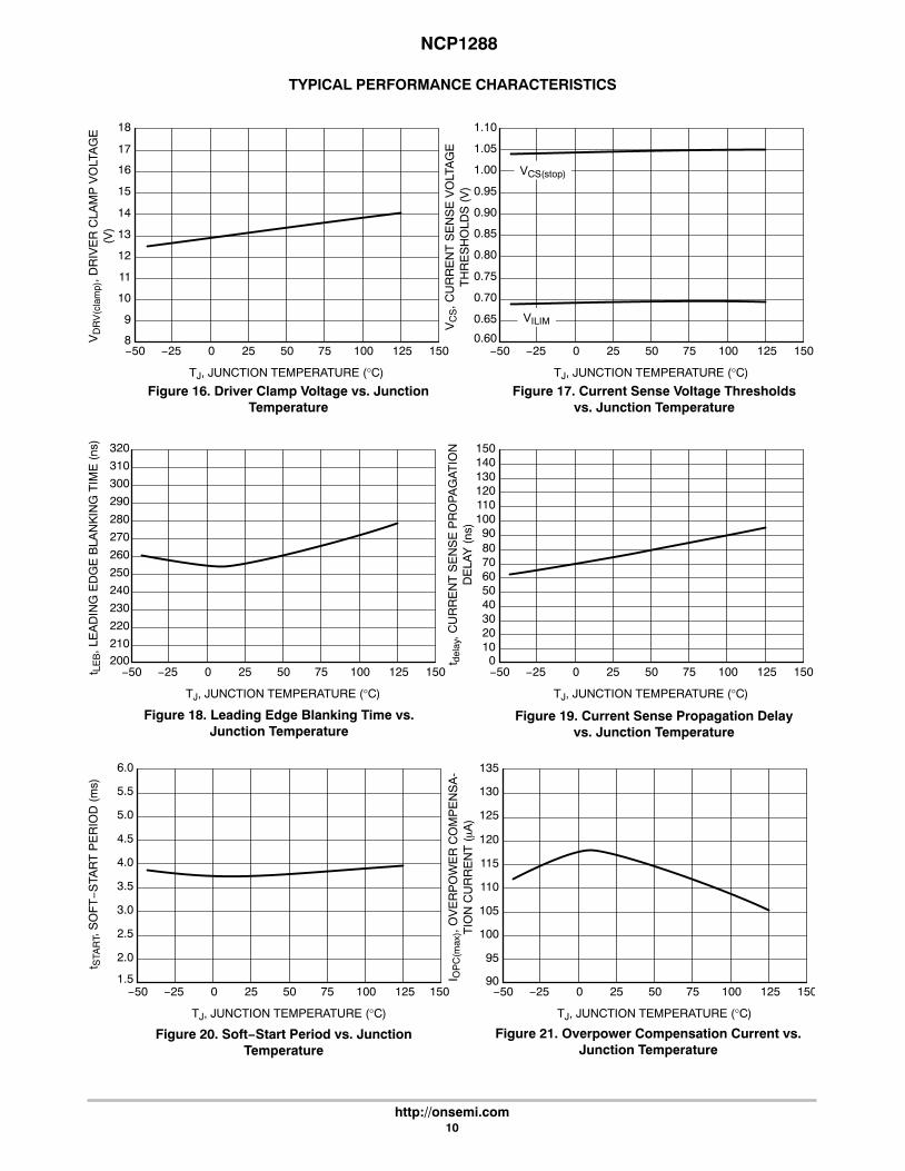
TYPICAL PERFORMANCE CHARACTERISTICS
TJ, JUNCTION TEMPERATURE (°C)
150125100250−508
10
12
14
16
VD
RV
(cla
mp)
, DR
IVE
R C
LAM
P V
OLT
AG
E(V
)
Figure 16. Driver Clamp Voltage vs. JunctionTemperature
Figure 17. Current Sense Voltage Thresholdsvs. Junction Temperature
Figure 18. Leading Edge Blanking Time vs.Junction Temperature
Figure 19. Current Sense Propagation Delayvs. Junction Temperature
Figure 20. Soft−Start Period vs. JunctionTemperature
7550−25
TJ, JUNCTION TEMPERATURE (°C)
150125100250−500.60
0.65
0.70
0.75
0.85
VC
S, C
UR
RE
NT
SE
NS
E V
OLT
AG
ET
HR
ES
HO
LDS
(V
)
7550−25
9
11
13
15
17
18
TJ, JUNCTION TEMPERATURE (°C)
150125100250−50200
220
240
260
280
t LE
B, L
EA
DIN
G E
DG
E B
LAN
KIN
G T
IME
(ns
)
7550−25
0.80
210
230
250
270
TJ, JUNCTION TEMPERATURE (°C)
150125100250−500
20
40
60
t del
ay, C
UR
RE
NT
SE
NS
E P
RO
PA
GA
TIO
ND
ELA
Y (
ns)
7550−25
10
30
50
70
TJ, JUNCTION TEMPERATURE (°C)
150125100250−501.5
2.0
2.5
3.0
4.5
t STA
RT,
SO
FT−
STA
RT
PE
RIO
D (
ms)
7550−25
3.5
4.0
TJ, JUNCTION TEMPERATURE (°C)
150125100250−5090
100
110
120
135
I OP
C(m
ax),
OV
ER
PO
WE
R C
OM
PE
NS
A-
TIO
N C
UR
RE
NT
(�A
)
7550−25
95
105
115
125
1.00
0.90
80
6.0
5.0
0.95
VILIM
VCS(stop)
290
310
300
320
Figure 21. Overpower Compensation Current vs.Junction Temperature
1.10
1.05
90
110
130
100
120
140150
5.5 130

NCP1288
http://onsemi.com11
TYPICAL PERFORMANCE CHARACTERISTICS
TJ, JUNCTION TEMPERATURE (°C)
150
125100250−504.84
4.88
4.92
4.96
5.00
VF
B(O
PC
), O
PC
VO
LTA
GE
TH
RE
SH
OLD
S (
V)
Figure 22. OPC FB Thresholds vs. JunctionTemperature
Figure 23. OPC Watchdog Time Thresholds vs.Junction Temperature
Figure 24. FB to CS Ratio vs. JunctionTemperature
Figure 25. FB Pull−up Resistor vs. JunctionTemperature
Figure 26. FB Pull−up Voltage vs. JunctionTemperature
7550−25
TJ, JUNCTION TEMPERATURE (°C)
150125100250−5030
31
32
33
35
t WD
, OP
C W
AT
CH
DO
G T
IME
(m
s)
7550−25
4.86
4.90
4.94
4.98
TJ, JUNCTION TEMPERATURE (°C)
150
125100250−501.10
1.20
1.30
1.40
1.50
KF
B, F
B T
O C
S R
AT
IO
7550−25
34
1.15
1.25
1.35
1.45
TJ, JUNCTION TEMPERATURE (°C)
150125100250−5015
17
19
21
RF
B(u
p), F
B P
ULL−
UP
RE
SIS
TO
R (
k�)
7550−25
16
18
20
22
TJ, JUNCTION TEMPERATURE (°C)
150125100250−504.34.44.54.6
4.9
VF
B(r
ef),
FB
PU
LL−
UP
VO
LTA
GE
(V
)
7550−25
4.74.8
TJ, JUNCTION TEMPERATURE (°C)
150125100250−5076
80
84
88
96
t faul
t, O
VE
RLO
AD
TIM
ER
DU
RA
TIO
N(m
s)
7550−25
78
82
86
90
38
36
23
5.2
5.0
37
VFB(OPCE)
VFB(OPC)
1.55
1.651.60
1.70
Figure 27. Overload Timer Duration vs. JunctionTemperature
41
39
24
26
25
27
5.1
92
1.751.80
40
5.3
5.6
5.45.5 94

NCP1288
http://onsemi.com12
TYPICAL PERFORMANCE CHARACTERISTICS
150
t aut
orec
, AU
TO
RE
CO
VE
RY
TIM
ER
DU
RA
TIO
N (
s)
Figure 28. Autorecovery Timer Duration vs.Junction Temperature
Figure 29. Brown−Out Detection TimerDuration vs. Junction Temperature
Figure 30. FB Thresholds for FrequencyFoldback vs. Junction Temperature
TJ, JUNCTION TEMPERATURE (°C)
150125100250−5058596061
63
t HV,
BO
DE
TE
CT
ION
TIM
ER
DU
RA
TIO
N(m
s)
7550−25
TJ, JUNCTION TEMPERATURE (°C)
125100250−501.26
1.30
1.34
1.38
1.42
7550−25
62
1.28
1.32
1.36
1.40
TJ, JUNCTION TEMPERATURE (°C)
150125100250−500.800.850.900.95
1.10
VF
B(f
old)
, FB
FO
LDB
AC
K T
HR
ES
HO
LDS
(V
)
7550−25
1.001.05
TJ, JUNCTION TEMPERATURE (°C)
150125100250−5023.0
24.0
25.0
26.0
28.0
f OS
C(m
in),
MIN
IMU
M S
WIT
CH
ING
FR
E-
QU
EN
CY
(m
s)
7550−25
23.5
24.5
25.5
26.5
66
64
1.25
1.15
65
VFB(endfold)
VFB(fold)
1.44
1.481.46
1.50
Figure 31. Minimum Switching Frequency vs.Junction Temperature
69
67
1.2027.0
1.521.54
68
1.30
1.45
1.351.40
27.5
7170
1.551.50
30.0
28.529.029.5
150
VS
kip,
SK
IP T
HR
ES
HO
LDS
(V
)
Figure 32. Skip Thresholds vs. JunctionTemperature
Figure 33. Soft−Skip Timer Duration vs.Junction Temperature
TJ, JUNCTION TEMPERATURE (°C)
150125100250−5070758085
95
t SS
KIP
, SO
FT−
SK
IP T
IME
R D
UR
AT
ION
(�s)
7550−25
TJ, JUNCTION TEMPERATURE (°C)
125100250−500.64
0.68
0.72
0.76
0.80
7550−25
90
0.66
0.70
0.74
0.78 110
100105
Vskip(in)
Vskip(out)0.82
0.86
0.84125
115120
135130
NCP1288
http://onsemi.com13
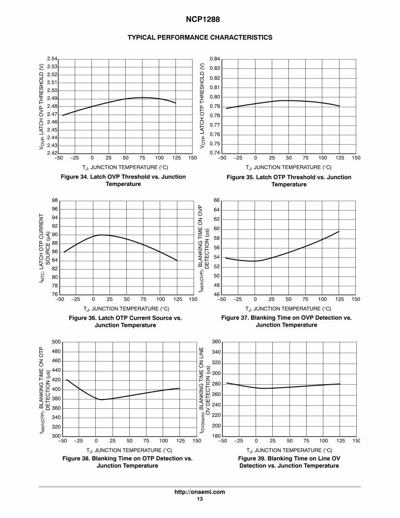
TYPICAL PERFORMANCE CHARACTERISTICS
TJ, JUNCTION TEMPERATURE (°C)
125100250−502.42
2.44
2.46
2.48
2.50
Figure 34. Latch OVP Threshold vs. JunctionTemperature
Figure 35. Latch OTP Threshold vs. JunctionTemperature
Figure 36. Latch OTP Current Source vs.Junction Temperature
7550−25
2.43
2.45
2.47
2.49
150
VO
VP,
LA
TC
H O
VP
TH
RE
SH
OLD
(V
)
TJ, JUNCTION TEMPERATURE (°C)
150125100250−500.74
0.76
0.78
0.80
VO
TP,
LA
TC
H O
TP
TH
RE
SH
OLD
(V
)
7550−25
0.75
0.77
0.79
0.81
TJ, JUNCTION TEMPERATURE (°C)
150125100250−5076
78
80
82
88
I NT
C, L
AT
CH
OT
P C
UR
RE
NT
SO
UR
CE
(�A
)
7550−25
84
86
TJ, JUNCTION TEMPERATURE (°C)
150125100250−5046
50
54
58
66t la
tch(
OV
P),
BLA
NK
ING
TIM
E O
N O
VP
DE
TE
CT
ION
(�s)
7550−25
48
52
56
60
0.82
94
90
Figure 37. Blanking Time on OVP Detection vs.Junction Temperature
0.83
0.84
9262
96
98
64
2.52
2.54
2.51
2.53
Figure 38. Blanking Time on OTP Detection vs.Junction Temperature
Figure 39. Blanking Time on Line OVDetection vs. Junction Temperature
TJ, JUNCTION TEMPERATURE (°C)
150125100250−50300
340
380
420
500
t latc
h(O
TP
), B
LAN
KIN
G T
IME
ON
OT
PD
ET
EC
TIO
N (�s)
7550−25
320
360
400
440
460
480
TJ, JUNCTION TEMPERATURE (°C)
150125100250−50180
220
260
300
t OV
(bla
nk),
BLA
NK
ING
TIM
E O
N L
INE
OV
DE
TE
CT
ION
(�s)
7550−25
200
240
280
320
340
360

NCP1288
http://onsemi.com14
TYPICAL PERFORMANCE CHARACTERISTICS
150
Vcl
amp(
Latc
h), L
AT
CH
PIN
CLA
MP
VO
LTA
GE
(V
)
Figure 40. Latch Pin Clamp Voltage vs. JunctionTemperature
TJ, JUNCTION TEMPERATURE (°C)
125100250−500.80
1.20
1.60
2.00
2.40
7550−25
1.00
1.40
1.80
2.20
Vclamp1(Latch)2.60
2.80
Vclamp0(Latch)

NCP1288
http://onsemi.com15
APPLICATION INFORMATION
Introduction
The NCP1288 includes all of the necessary features to builda safe and efficient power supply based on afixed−frequency flyback converter. It is particularly wellsuited for applications where low part count is a keyparameter, without sacrificing safety.• Current−Mode Operation with slope compensation:
The primary peak current is permanently controlled bythe FB voltage, ensuring maximum safety: the DRVturn−off event is dictated by the peak current setpoint.It also ensures that the frequency response of thesystem remains first order if in DCM, which eases thedesign of the feedback loop. The controller can also beused in CCM with a wide input voltage range due to itsfixed ramp compensation that prevents the appearanceof sub−harmonic oscillations in most of theapplications.
• Fixed−Frequency Oscillator with Jittering: TheNCP1288 is available in various frequency options tofit any application. The internal oscillator features alow−frequency jittering that helps to pass the EMIrequirements by spreading out the energy content offrequency peaks in quasi−peak and average mode.
• Latched / Autorecovery Timer−Based OvercurrentProtection: The overcurrent protection depends onlyon the FB signal, enabling it to work with anytransformer, even with very poor coupling or highleakage inductance. The protection is fully latched onthe A version (the power supply has to be unpluggedthen restarted in order to resume operation, even if theoverload condition disappears), and autorecovery on theB version. The timer’s duration is fixed. The controlleralso enters the same protection mode if the voltage onthe CS pin reaches 1.5 times the maximum internalsetpoint, which enables to detect winding short circuits.
• High Voltage Startup Current Source withBrown−Out and Line Overvoltage Detections: Dueto On Semiconductor’s Very High Voltage technology,the NCP1288 can directly be connected to the highinput voltage. The startup current source ensures aclean startup while ensuring low losses when it is off.The high voltage pin also features a high−voltagesensing circuitry, which is able to turn the controller offif the input voltage is too low (brown−out condition) ortoo high (line overvoltage). This protection workseither with a DC input voltage or a rectified AC inputvoltage, and is independent of the high voltage ripple. Ituses a peak detector synchronized with line frequency,or with the internal watchdog timer if the HV pin is tiedto a dc voltage.
• Adjustable Overpower Compensation: The highvoltage sensed on the HV pin is converted into acurrent to add to the current sense voltage an offset
proportional to the input voltage. By choosing the valueof the resistor in series with the CS pin, the amount ofcompensation can be adjusted to the application.
• Frequency foldback then Soft−Skip mode for lightload operation: In order to ensure a high efficiency inall load conditions, the NCP1288 implements afrequency foldback (the switching frequency is loweredto reduce switching losses) for light load condition; anda Soft−Skip (disabled in case of fast load transients) forextremely low load condition.
• Extended VCC range: The NCP1288 accepts a supplyvoltage as high as 28 V, making the design of the powersupply easier.
• Clamped Driver Stage: Despite the high supplyvoltage, the voltage on DRV pin is safely clampedbelow 16 V; allowing the use of any standard MOSFET,and reducing the current consumption of the controller.
• Dual Latch−off Input: The NCP1288 can be latchedoff by an increasing voltage applied to its Latch pin(typically an overvoltage) or by a decreasing one, andan NTC can be directly connected to the latch pinthanks to the precise internal current source.
• Soft−Start: At every startup the peak current isgradually increased during 4 ms to minimize the stresson power components.
• Temperature Shutdown: The NCP1288 is internallyprotected against self−heating: if the die temperature istoo high, the controller shuts all circuitries down(including the HV startup current source), allowing thesilicon to cool down before attempting to restart. Thisensures a safe behavior in case of failure.
Typical Operation• Startup: The HV startup current source ensures the
charging of the VCC capacitor up to the startupthreshold VCC(on), until the input voltage is highenough (above VHV(start)) to enable the switching. Thecontroller then delivers pulses, starting with a soft−startperiod tSSTART during which the peak current linearlyincreases before the current−mode control takes over.During the soft−start period, the low level latch isignored, and the latch current is double, to ensure a fastpre−charge of the decoupling capacitor on the Latchpin.
• Normal operation: As long as the feedback voltage iswithin the regulation range, the NCP1288 runs at afixed frequency (with jittering) in current−modecontrol, where the peak current (sensed on the CS pin)is set by the voltage on the FB pin. A fixed rampcompensation is applied internally to preventsub−harmonic oscillations from occurring. The VCCmust be supplied by an external source (such as an

NCP1288
http://onsemi.com16
auxiliary winding), as the startup current source cannotpermanently supply the controller without overheating.
• Light load operation: When the FB voltage decreasesbelow VFB(fold), typically corresponding to a load of16% of the maximum load (for a DCM design), theswitching frequency starts to decrease down tofOSC(min). By lowering the switching losses, this featurehelps to improve the efficiency in light load conditions.The frequency jittering is disabled in light loadoperation.
• No load operation: When the FB voltage decreasesbelow Vskip(in), typically corresponding to a load of 1%of the maximum load, the controller enters Skip mode.By completely stopping the switching while thefeedback voltage is below Vskip(out), the losses arefurther reduced, allowing to minimize the powerdissipation under extremely low load conditions. Inorder to avoid audible noise, the peak current isgradually increased during the tSSKIP duration whileexiting the skip mode (Soft−Skip function). In case ofabrupt load increase during Soft−Skip mode, thesoft−skip portion is bypassed and the peak currentneeded for regulation is directly applied.
• Overload: The NCP1288 features a timer−basedoverload detection, solely dependent on the feedback
information: as soon as the internal peak currentsetpoint hits the VILIM clamp, the internal overloadtimer starts to count. When the timer times out, thecontroller stops and enter the protection mode,autorecovery for the B version (the controller initiates anew start−up after tautorec elapses), or latched for the Aversion (the latch is released if a brown−out eventoccurs or VCC is reset).
• Brown−out: The NCP1288 features on its HV pin atrue AC line monitoring circuitry, which includes aminimum startup threshold, brown−out protection, andovervoltage protection. All of these circuits areautorecovery and operate independently of any rippleon the input voltage. They can even work with anunfiltered, rectified AC input. All thresholds are fixed,but they are designed to fit most of the standard ac−dcconversion applications.
• Latch−off: When the Latch input is pulled up (typicallyby an overvoltage condition), or pulled low (typicallyby an overtemperature condition, using the providedcurrent source with an NTC), the controller latches off.The latch is released when a brown−out conditionoccurs, or when VCC decreases below VCC(reset).

NCP1288
http://onsemi.com17
DETAILED DESCRIPTION
High−Voltage Current Source (Dynamic Self−Supply)with Built−in Brown−out Detection
The NCP1288 HV pin can be connected either to therectified bulk voltage, or to the ac line through a rectifier.
Startup
−+
−+
+
+
R
SQ
TSD
HV
VCC
Istart
VCC(on)
VCC(min)
tUVLO(blank)
blanking
Control
UVLO
−+
+
VCC(reset)
Reset
IC Start
Figure 41. HV Startup Current Source Functional Schematic

NCP1288
http://onsemi.com18
At startup, the current source turns on when the voltage onthe HV pin is higher than VHV(min), and turns off when VCCreaches VCC(on). It turns on again when VCC reachesVCC(min). This sequence repeats until the input voltage ishigh enough to ensure a proper startup, i.e. when VHVreaches VHV(start). The switching actually starts the next
time VCC reaches VCC(on), as shown in Figure 5. The currentsource is then turned off, saving additional power when theVCC is supplied externally.
Once the controller has started, if VCC reaches VCC(min)the switching stops and the protection mode is activated: thecontroller must be supplied by an external voltage source.
Figure 42. Startup Timing Diagram
time
VHV
time
VCC
time
DRV
VHV(start)
VHV(min)
VCC(on)
VCC(min)
VCC(inhibit)
HV
current
source =
Istart1
HV
current
source =
Istart2
Waits
next
VCC(on)
before
starting

NCP1288
http://onsemi.com19
To reduce the power dissipation in case the VCC pin isshorted to GND (in case of VCC capacitor failure, or externalpulldown on VCC to disable the controller), the startupcurrent is lowered when VCC is below VCC(inhibit).
There are only two conditions for which the current sourcedoesn’t turn on when VCC reaches VCC(min): the voltage onHV pin is too low (below VHV(min)), or a thermal shutdowncondition (TSD) has been detected. In all other conditions,the HV current source always turns on and off to maintainVCC between VCC(min) and VCC(on).
Brown−out and Line OvervoltageWhen the input voltage goes below VHV(stop), a
brown−out condition is detected, and the controller stops.The HV current source alternatively turns on and off tomaintain VCC between VCC(on) and VCC(min) until the inputvoltage is back above VHV(start).
The same situation occurs when an overvoltage isdetected on the ac line, i.e. when the input voltage goesabove VHV(OV): the controller stops, and resumes normaloperation when the overvoltage condition has gone.
Figure 43. Brown−out or Line Overvoltage Timing Diagram
time
HV stop
time
VCC
time
DRV
VCC(on)
VCC(min)
Waits next
VCC(on) before
starting
Brown-out
or AC OVP
detected

NCP1288
http://onsemi.com20
When VHV crosses the VHV(start) threshold, the controllercan start immediately. When it crosses VHV(stop), it triggers
a timer of duration tHV: this ensures that the controllerdoesn’t stop in case of line cycle drop−out.
Figure 44. AC Input Brown−out Timing Diagram
time
VHV
time
DRV
VHV(start)
Starts at next
VCC(ON)
VHV(stop)
Brown-out
HVt
The same scheme is used for the Line OVP, except that thistime the controller must not stop instantaneously when theinput voltage goes above VHV(OV1). In order to be
insensitive to spikes and voltage surges a blanking circuit isinserted after the output of the comparator, with a durationof tOV(blank).

NCP1288
http://onsemi.com21
Figure 45. AC Input Line Overvoltage Timing Diagram
time
VHV
time
One Shot
time
DRV
VHV(OV1)
OVP
detected
HV
timer
starts
Blanked
voltage
surge
HV
timer
restarts
Restarts at
VCC(on)
VHV(OV2)
HVt

NCP1288
http://onsemi.com22
Oscillator with Maximum Duty Ratio and FrequencyJittering
The NCP1288 includes an oscillator that sets theswitching frequency with an accuracy of �7%. Themaximum duty ratio of the DRV pin is 80% (typical), withan accuracy of �7%.
In order to improve the EMI signature, the switchingfrequency jitters around its nominal value, with atriangle−wave shape.
Figure 46. Frequency Jittering
Time
fOSC
fOSC + Ajitter
Nominal fOSC
fOSC - Ajitter
1 / Fjitter
Clamped DriverThe supply voltage for the NCP1288 can be as high as
28 V, but most of the MOSFETs that will be connected to theDRV pin cannot tolerate a gate−to−source voltage greaterthan 20 V on their gate. The driver pin is therefore clampedsafely below 16 V.
Figure 47. Clamped Driver
DRV
Clamp
DRV signal
VCC
This driver has a typical current capability of ±1.0 A.
NCP1288
http://onsemi.com23
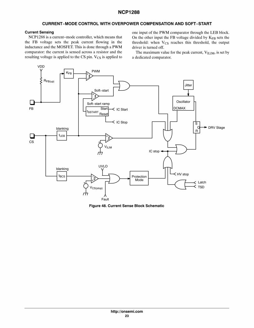
CURRENT−MODE CONTROL WITH OVERPOWER COMPENSATION AND SOFT−START
Current SensingNCP1288 is a current−mode controller, which means that
the FB voltage sets the peak current flowing in theinductance and the MOSFET. This is done through a PWMcomparator: the current is sensed across a resistor and theresulting voltage is applied to the CS pin. VCS is applied to
one input of the PWM comparator through the LEB block.On the other input the FB voltage divided by KFB sets thethreshold: when VCS reaches this threshold, the outputdriver is turned off.
The maximum value for the peak current, VILIM, is set bya dedicated comparator.
Figure 48. Current Sense Block Schematic
CS
FB
−+
tLEB
blanking
KFB
VDD
RFB(up)
−+
−+
−+
+
+
VILIM
VCS(stop)
S
RQ
tSSTART
Soft−start ramp
Start
ResetIC Start
IC Stop
Oscillator
DCMAX
ProtectionMode
UVLO
Jitter
HV stop
Latch
Soft−start
IC stop
TSD
Fault
DRV Stage
blanking
PWM
tBCS

NCP1288
http://onsemi.com24
Each time the controller is starting, i.e. the controller wasoff and starts, or restarts, when VCC reaches VCC(on), asoft−start is applied: the current sense setpoint is linearlyincreased from 0 (the minimum level can be higher than 0
because of the LEB and propagation delay) until it reachesVILIM (after a duration of tSSTART), or until the FB loopimposes a setpoint lower than the one imposed by thesoft−start (the 2 comparators outputs are OR’ed).
Figure 49. Soft−Start
Time
VFB
VFB(fault)
Time
Soft-start ramp
VILIM
tSSTART
Time
CS Setpoint
VILIMI
VFB takes
over soft-start
Under some conditions, like a winding short−circuit forinstance, not all the energy stored during the on time istransferred to the output during the off time, even if the ontime duration is at its minimum (imposed by the propagationdelay of the detector added to the LEB duration). As a result,the current sense voltage keeps on increasing above VILIM,because the controller is blind during the LEB blanking
time. Dangerously high current can grow in the system ifnothing is done to stop the controller. In order to protectagainst this, an additional comparator is included, thatsenses when VCS reaches VCS(stop) ( = 1.5 x VILIM ). As soonas this comparator toggles, the controller immediately entersthe protection mode (latched or autorecovery according tothe chosen option).

NCP1288
http://onsemi.com25
Compensation for Overpower DetectionThe power delivered by a flyback power supply is
proportional to the square of the peak current:
POUT �1
2� � � LP � FSW � IP
2 (eq. 1)
(in discontinuous conduction mode).
Unfortunately, due to the inherent propagation delay ofthe logic, the actual peak current is higher at high inputvoltage than at low input voltage, as shown in Figure 50.This leads to a significant difference in the maximum outputpower delivered by the power supply.
Figure 50. Line Compensation for True Overpower Protection
time
IP
High
LineLow
Line
ILIMIT
tdelay tdelay
IP to be
compensated
To compensate this and have an accurate overpowerprotection, an offset proportional to the input voltage isadded to the CS signal by turning on an internal currentsource (IOPC): by adding an external resistor (ROPC) inseries between the sense resistor and the CS pin, a voltageoffset is created across it by the current. The compensationcan be adjusted by changing the value of the ROPC resistor.
Since in light load conditions this offset is in the sameorder of magnitude as the current sense signal, it must beremoved. Therefore the compensation current is only addedwhen the FB voltage is higher than VFB(OPC), as shown inFigure 52.
Figure 51. Schematic Overpower Compensation Circuit
HVV to I
CS
t LEB
blankingTo CSblock
VDD
IOPC = 0.5� x (VHV − 125)
FB
−
+
+
VFB(OPC)
HV Sensing
ROPC
Rsense
NCP1288
http://onsemi.com26
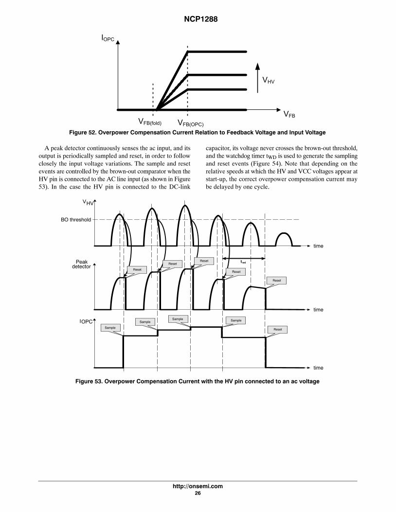
Figure 52. Overpower Compensation Current Relation to Feedback Voltage and Input Voltage
VFB
IOPC
VFB(fold) VFB(OPC)
VHV
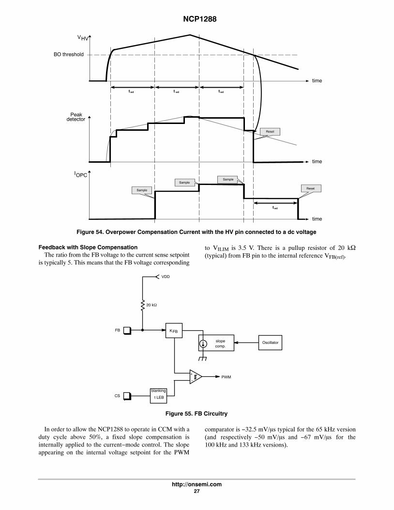
A peak detector continuously senses the ac input, and itsoutput is periodically sampled and reset, in order to followclosely the input voltage variations. The sample and resetevents are controlled by the brown-out comparator when theHV pin is connected to the AC line input (as shown in Figure53). In the case the HV pin is connected to the DC-link
capacitor, its voltage never crosses the brown-out threshold,and the watchdog timer tWD is used to generate the samplingand reset events (Figure 54). Note that depending on therelative speeds at which the HV and VCC voltages appear atstart-up, the correct overpower compensation current maybe delayed by one cycle.
time
VHV
time
Peakdetector
twd
time
IOPCSample
SampleSample Sample
Reset
ResetReset
Reset
Reset
Reset
BO threshold
Figure 53. Overpower Compensation Current with the HV pin connected to an ac voltage
NCP1288
http://onsemi.com27
time
time
VHV
Peakdetector
time
IOPC
BO threshold
t wd
Sample
SampleSample
Reset
Reset
t wd t wd
twd
Figure 54. Overpower Compensation Current with the HV pin connected to a dc voltage
Feedback with Slope CompensationThe ratio from the FB voltage to the current sense setpoint
is typically 5. This means that the FB voltage corresponding
to VILIM is 3.5 V. There is a pullup resistor of 20 k�(typical) from FB pin to the internal reference VFB(ref).
Figure 55. FB Circuitry
CS
FB
−
+
t LEB
blanking
VDD
Oscillator
20 k�
KFB
slopecomp.
PWM
In order to allow the NCP1288 to operate in CCM with aduty cycle above 50%, a fixed slope compensation isinternally applied to the current−mode control. The slopeappearing on the internal voltage setpoint for the PWM
comparator is −32.5 mV/�s typical for the 65 kHz version(and respectively −50 mV/�s and −67 mV/�s for the100 kHz and 133 kHz versions).

NCP1288
http://onsemi.com28
OVERCURRENT PROTECTION WITH FAULT TIMER
Classical Overcurrent ProtectionWhen an overcurrent occurs on the output of the power
supply, the feedback loop asks for more power than thecontroller can deliver, and the CS setpoint reaches VILIM.When this event occurs, an internal tfault timer is started:once the timer times out, DRV pulses are stopped and the
controller is either latched off (latched protection,Version A), or it enters an autorecovery mode (Version B).The timer is reset when the CS setpoint goes back belowVILIM before the timer elapses. The fault timer is also startedif the driver signal is reset by the max duty ratio.
Figure 56. Timer−Based Overcurrent Protection
CS
FB−+
tLEB
blanking
/ 5
−+
+
VILIM
ProtectionMode
Brown−out
tfault
timer
release
t autorec
timer
Reset
Autorecoveryprotectionmode only
R
SQ
PWM
Reset DRV
Fault Flag
DC MAX
DRV
In autorecovery mode, the controller tries to restart aftertautorec. If the fault has gone, the supply resumes operation;if not, the system starts a new burst cycle (see Figure 57).

NCP1288
http://onsemi.com29
Figure 57. Autorecovery Timer−Based Protection Mode
time
Fault Flag
time
VCC
time
DRV
VCC(on)
VCC(min)
Overcurrent
applied
time
Output Load
Max Load
time
Fault timer
tfault
Fault
timer
starts
Controller
stops
Fault
disappears
tfault tautorec
RestartAt VCC(on)(new burst
cycle if Fault
still present)
NCP1288
http://onsemi.com30
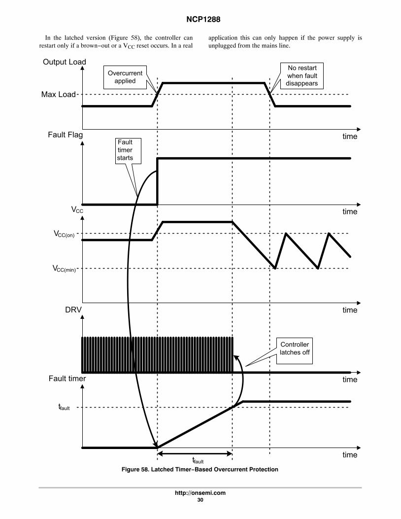
In the latched version (Figure 58), the controller canrestart only if a brown−out or a VCC reset occurs. In a real
application this can only happen if the power supply isunplugged from the mains line.
Figure 58. Latched Timer−Based Overcurrent Protection
time
Fault Flag
time
VCC
time
DRV
VCC(on)
VCC(min)
Overcurrent
applied
time
Output Load
Max Load
time
Fault timer
tfault
Fault
timer
starts
Controller
latches off
No restart
when faultdisappears
tfault

NCP1288
http://onsemi.com31
If VCC reaches VCC(min) before the timer has elapsed, thecontroller enters protection mode anyway (in both
protection mode versions). Here is the example with thelatched version:
Overcurrentapplied
Fault timer starts
Controller latches off
No restartwhen fault disappears
Figure 59. Overcurrent Protection Mode Triggered by VCC
Output Load
Fault Flag
Fault Timer
DRV
time
time
time
time
time
VCC
VCC(on)
VCC(min)
Max Load
tfault
tfault

NCP1288
http://onsemi.com32
LOW LOAD OPERATION
Frequency FoldbackIn order to improve the efficiency in light load conditions,
the frequency of the internal oscillator is linearly reducedfrom its nominal value down to fOSC(min). This frequencyfoldback starts when the voltage on FB pin goes belowVFB(fold), and is complete before VFB reaches Vskip(in),
whatever the nominal switching frequency option is. Thecurrent−mode control is still active while the oscillatorfrequency decreases, but the frequency jittering is off.
Note that the frequency foldback is disabled if thecontroller runs at its maximum duty cycle.
Figure 60. Frequency Foldback when the FB Voltage Decreases
FB
fOSC
Nominal fOSC
Vskip(in) VFB(fold)
fOSC(min)
Skip
Skip Cycle Mode with Soft−Skip
Figure 61. Skip Cycle with Soft−Skip Schematic
−+
DRV stage
CS
S
RQ
tSSKIP
Soft−skip ramp
FB
Reset
tLEB
blanking
OscillatorDCMAX
−+
KFB
+
Vskip
Sawtooth
−+
When VFB reaches Vskip(in) while decreasing, the skipmode is activated: the driver stops, and the internalconsumption of the controller is decreased. While VFB isbelow Vskip(out), the controller remains in this state. WhenVFB crosses Vskip(out), the DRV pin starts to pulse again, and
the controller restarts with a short Soft−Skip duration(tSSKIP). The soft−skip imposes the peak current from nearly0, in a voltage−mode manner: it doesn’t have the samebehavior as the startup soft−start which is current−modedriven.
NCP1288
http://onsemi.com33
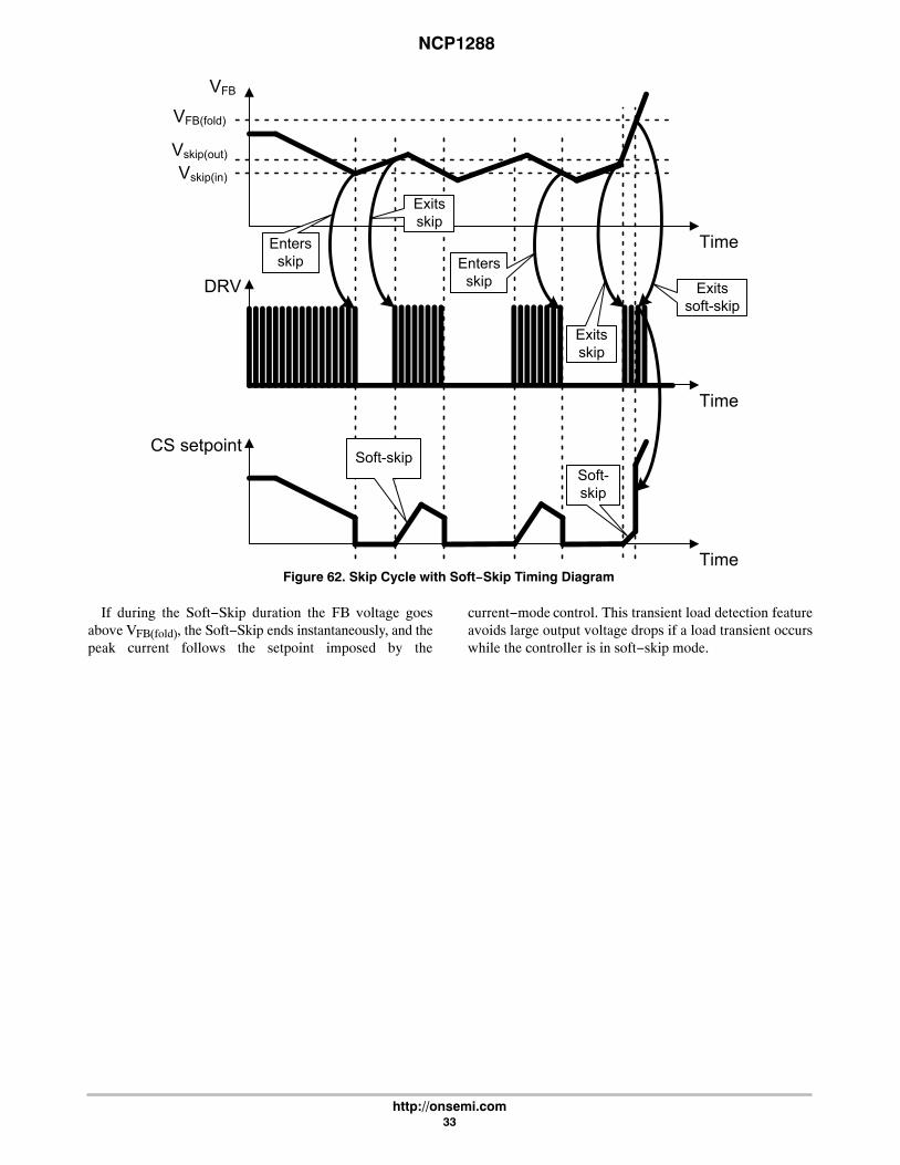
Figure 62. Skip Cycle with Soft−Skip Timing Diagram
Time
VFB
Vskip(out)
Time
DRV
Time
CS setpointSoft-skip
Enters
skip
Exits
skip
Enters
skip
Exits
skip
Soft-
skip
Exits
soft-skip
Vskip(in)
VFB(fold)
If during the Soft−Skip duration the FB voltage goesabove VFB(fold), the Soft−Skip ends instantaneously, and thepeak current follows the setpoint imposed by the
current−mode control. This transient load detection featureavoids large output voltage drops if a load transient occurswhile the controller is in soft−skip mode.

NCP1288
http://onsemi.com34
Latch−off Input
Figure 63. Latch Detection Schematic
−+
Latch
VOVP
S
RQ
−+
VOTP
tLatch(OVP)
blankingVDD
Brown−outReset
Latch
Vclamp
INTC
tLatch(OTP)
blanking
1 k�
INTC
+
+
Soft−startend
The Latch pin is dedicated to the latch−off function. Itincludes two thresholds that define a working window,between a high latch and a low latch. Within these 2thresholds; the controller is allowed to run; but as soon aseither the low or the high threshold is crossed, the controlleris latched off. The lower threshold is intended to be usedwith an NTC thermistor, with the internal current sourceINTC providing the necessary bias current.
An active clamp prevents the voltage from reaching thehigh threshold if it is only pulled up by the ILatch current. Toreach the high threshold, the pullup current has to be higherthan the pulldown capability of the clamp (typically 1.5 mAat VOVP).
To avoid any false triggering, noise spikes shorter thantLatch(OVP) or tLatch(OTP) respectively are blanked, and onlylonger events can actually latch the controller.
Reset occurs when a brown−out condition is detected orthe VCC is cycled down to a VCC(reset), which in a realapplication can only happen if the power supply isunplugged from the AC line.
Upon startup, the internal references take some timebefore reaching their nominal values; and one of thecomparators could toggle inadvertantly. Therefore theinternal logic ignores the latch signal before the controller isready to start. Once VCC reaches VCC(on), the latch pin Highlatch state is enabled and the DRV switching starts only if itis allowed; whereas the Low latch (typically sensing anovertemperature) is taken into account only after thesoft−start is finished. In addition, the NTC current is doubledduring the soft−start period, to speed up the charging of theLatch pin capacitor.

NCP1288
http://onsemi.com35
Figure 64. Latch−off Function Timing Diagram
time
Internal Latch Signaltime
VCC
time
DRV
VCC(on)
VCC(min)
Latch signal
high during
pre-start phase
Noise spike
ignored
(tLatch blanking)
Start-up
initiated by
VCC(on)
Switching
allowed (no
latch event)
Latch-off
Temperature shutdownThe die includes a temperature shutdown protection with
a turn−off threshold guaranteed between 140°C and 160°C,and a typical hysteresis of 30°C. When the temperature risesabove the high threshold, the controller stops switching
instantaneously, the HV current source is turned off, and theinternal logic state is reset.
When the temperature falls below the low threshold, theHV startup current source is enabled, and a regular startupsequence takes place.

NCP1288
http://onsemi.com36
STATE DIAGRAMS
HV Startup Current Source
Figure 65. HV Startup Current Source State Diagram
Stop
Istart1
Istart2
Off
No TSD
TSD
TSD
VCC > VCC(inhibit)
VCC < VCC(inhibit)
VCC > VCC(on)
VCC < VCC(min)
TSD
TSD

NCP1288
http://onsemi.com37
Controller Operation (Latched Version: A Option)
Figure 66. Controller Operation State Diagram (Latched Protection)
Stopped
Running
� Brown-out
� HV OVP� TSD
VCC > VCC(on)
� Brown-out
� HV OVP� TSD
Skip out
With Fault = � tfault
CS > VCS(stop)
� VCC < VCC(min)
Soft−start
Soft−skip
� Soft-skip ends
� VFB> VFB(fold)
Soft-start ends
Skip
Skip in
� Brown-out
� HV OVP� TSD
� Brown-out
� HV OVP� TSD
� Brown-out
� HV OVP� TSD
Latch
� Brown-out
� VCC reset
High Latch
� High Latch
� Low Latch
� High Latch
� Low Latch
� Fault
� High Latch� Low Latch
� Vexpires

NCP1288
http://onsemi.com38
Controller Operation (Autorecovery Version: B Option)
Figure 67. Controller Operation State Diagram (Autorecovery Protection)
Stopped
Running
� Fault
� Brown-out� HV OVP
� TSD
VCC > VCC(on)
� tautorec counting� Brown-out
� HV OVP
� TSD
Skip out
With Fault = � tfault expires
� VCS > VCS(stop)
� VCC < VCC(min)
Soft−start
Soft−skip
� Soft-skip ends
� VFB > VFB(fold)
Soft-start ends
Skip
Skip in
� Brown-out
� HV OVP
� TSD
� Brown-out
� HV OVP� TSD
� Brown-out
� HV OVP� TSD
Latch
� Brown-out
� VCC reset
High Latch
� High Latch
� Low Latch
� High Latch
� Low Latch
� High Latch
� Low Latch
Table 1. ORDERING INFORMATION
Part No. Overload Protection Switching Frequency Package Shipping†
NCP1288BD65R2G Autorecovery 65 kHz SOIC−7(Pb−Free)
2500 / Tape & Reel
†For information on tape and reel specifications, including part orientation and tape sizes, please refer to our Tape and Reel PackagingSpecifications Brochure, BRD8011/D.
Soft−Skip is a trademark of Semiconductor Components Industries, LLC (SCILLC).
SOIC−7CASE 751U−01
ISSUE EDATE 20 OCT 2009
SEATINGPLANE
14
58
R
J
X 45�
K
NOTES:1. DIMENSIONING AND TOLERANCING PER
ANSI Y14.5M, 1982.2. CONTROLLING DIMENSION: MILLIMETER.3. DIMENSION A AND B ARE DATUMS AND T
IS A DATUM SURFACE.4. DIMENSION A AND B DO NOT INCLUDE
MOLD PROTRUSION.5. MAXIMUM MOLD PROTRUSION 0.15 (0.006)
PER SIDE.
S
DH
C
SCALE 1:1
DIMA
MIN MAX MIN MAXINCHES
4.80 5.00 0.189 0.197
MILLIMETERS
B 3.80 4.00 0.150 0.157C 1.35 1.75 0.053 0.069D 0.33 0.51 0.013 0.020G 1.27 BSC 0.050 BSCH 0.10 0.25 0.004 0.010J 0.19 0.25 0.007 0.010K 0.40 1.27 0.016 0.050M 0 8 0 8 N 0.25 0.50 0.010 0.020S 5.80 6.20 0.228 0.244
−A−
−B−
G
MBM0.25 (0.010)
−T−
BM0.25 (0.010) T S A S
M
XXX = Specific Device CodeA = Assembly LocationL = Wafer LotY = YearW = Work Week� = Pb−Free Package
GENERICMARKING DIAGRAM
7 PL� � � �
*This information is generic. Please refer todevice data sheet for actual part marking.Pb−Free indicator, “G” or microdot “ �”,may or may not be present.
XXXXXALYWX
�1
8
STYLES ON PAGE 2
1.520.060
7.00.275
0.60.024
1.2700.050
4.00.155
� mminches
�SCALE 6:1
*For additional information on our Pb−Free strategy and solderingdetails, please download the ON Semiconductor Soldering andMounting Techniques Reference Manual, SOLDERRM/D.
SOLDERING FOOTPRINT*
MECHANICAL CASE OUTLINE
PACKAGE DIMENSIONS
ON Semiconductor and are trademarks of Semiconductor Components Industries, LLC dba ON Semiconductor or its subsidiaries in the United States and/or other countries.ON Semiconductor reserves the right to make changes without further notice to any products herein. ON Semiconductor makes no warranty, representation or guarantee regardingthe suitability of its products for any particular purpose, nor does ON Semiconductor assume any liability arising out of the application or use of any product or circuit, and specificallydisclaims any and all liability, including without limitation special, consequential or incidental damages. ON Semiconductor does not convey any license under its patent rights nor therights of others.
98AON12199DDOCUMENT NUMBER:
DESCRIPTION:
Electronic versions are uncontrolled except when accessed directly from the Document Repository.Printed versions are uncontrolled except when stamped “CONTROLLED COPY” in red.
PAGE 1 OF 27−LEAD SOIC
© Semiconductor Components Industries, LLC, 2019 www.onsemi.com

SOIC−7CASE 751U−01
ISSUE EDATE 20 OCT 2009
STYLE 4:PIN 1. ANODE
2. ANODE3. ANODE4. ANODE5. ANODE6. ANODE7. NOT USED8. COMMON CATHODE
STYLE 1:PIN 1. EMITTER
2. COLLECTOR3. COLLECTOR4. EMITTER5. EMITTER6.7. NOT USED8. EMITTER
STYLE 2:PIN 1. COLLECTOR, DIE, #1
2. COLLECTOR, #13. COLLECTOR, #24. COLLECTOR, #25. BASE, #26. EMITTER, #27. NOT USED8. EMITTER, #1
STYLE 3:PIN 1. DRAIN, DIE #1
2. DRAIN, #13. DRAIN, #24. DRAIN, #25. GATE, #26. SOURCE, #27. NOT USED8. SOURCE, #1
STYLE 6:PIN 1. SOURCE
2. DRAIN3. DRAIN4. SOURCE5. SOURCE6.7. NOT USED8. SOURCE
STYLE 5:PIN 1. DRAIN
2. DRAIN3. DRAIN4. DRAIN5.6.7. NOT USED8. SOURCE
STYLE 7:PIN 1. INPUT
2. EXTERNAL BYPASS3. THIRD STAGE SOURCE4. GROUND5. DRAIN6. GATE 37. NOT USED8. FIRST STAGE Vd
STYLE 8:PIN 1. COLLECTOR (DIE 1)
2. BASE (DIE 1)3. BASE (DIE 2)4. COLLECTOR (DIE 2)5. COLLECTOR (DIE 2)6. EMITTER (DIE 2)7. NOT USED8. COLLECTOR (DIE 1)
STYLE 9:PIN 1. EMITTER (COMMON)
2. COLLECTOR (DIE 1)3. COLLECTOR (DIE 2)4. EMITTER (COMMON)5. EMITTER (COMMON)6. BASE (DIE 2)7. NOT USED8. EMITTER (COMMON)
STYLE 10:PIN 1. GROUND
2. BIAS 13. OUTPUT4. GROUND5. GROUND6. BIAS 27. NOT USED8. GROUND
STYLE 11:PIN 1. SOURCE (DIE 1)
2. GATE (DIE 1)3. SOURCE (DIE 2)4. GATE (DIE 2)5. DRAIN (DIE 2)6. DRAIN (DIE 2)7. NOT USED8. DRAIN (DIE 1)
ON Semiconductor and are trademarks of Semiconductor Components Industries, LLC dba ON Semiconductor or its subsidiaries in the United States and/or other countries.ON Semiconductor reserves the right to make changes without further notice to any products herein. ON Semiconductor makes no warranty, representation or guarantee regardingthe suitability of its products for any particular purpose, nor does ON Semiconductor assume any liability arising out of the application or use of any product or circuit, and specificallydisclaims any and all liability, including without limitation special, consequential or incidental damages. ON Semiconductor does not convey any license under its patent rights nor therights of others.
98AON12199DDOCUMENT NUMBER:
DESCRIPTION:
Electronic versions are uncontrolled except when accessed directly from the Document Repository.Printed versions are uncontrolled except when stamped “CONTROLLED COPY” in red.
PAGE 2 OF 27−LEAD SOIC
© Semiconductor Components Industries, LLC, 2019 www.onsemi.com

onsemi, , and other names, marks, and brands are registered and/or common law trademarks of Semiconductor Components Industries, LLC dba “onsemi” or its affiliatesand/or subsidiaries in the United States and/or other countries. onsemi owns the rights to a number of patents, trademarks, copyrights, trade secrets, and other intellectual property.A listing of onsemi’s product/patent coverage may be accessed at www.onsemi.com/site/pdf/Patent−Marking.pdf. onsemi reserves the right to make changes at any time to anyproducts or information herein, without notice. The information herein is provided “as−is” and onsemi makes no warranty, representation or guarantee regarding the accuracy of theinformation, product features, availability, functionality, or suitability of its products for any particular purpose, nor does onsemi assume any liability arising out of the application or useof any product or circuit, and specifically disclaims any and all liability, including without limitation special, consequential or incidental damages. Buyer is responsible for its productsand applications using onsemi products, including compliance with all laws, regulations and safety requirements or standards, regardless of any support or applications informationprovided by onsemi. “Typical” parameters which may be provided in onsemi data sheets and/or specifications can and do vary in different applications and actual performance mayvary over time. All operating parameters, including “Typicals” must be validated for each customer application by customer’s technical experts. onsemi does not convey any licenseunder any of its intellectual property rights nor the rights of others. onsemi products are not designed, intended, or authorized for use as a critical component in life support systemsor any FDA Class 3 medical devices or medical devices with a same or similar classification in a foreign jurisdiction or any devices intended for implantation in the human body. ShouldBuyer purchase or use onsemi products for any such unintended or unauthorized application, Buyer shall indemnify and hold onsemi and its officers, employees, subsidiaries, affiliates,and distributors harmless against all claims, costs, damages, and expenses, and reasonable attorney fees arising out of, directly or indirectly, any claim of personal injury or deathassociated with such unintended or unauthorized use, even if such claim alleges that onsemi was negligent regarding the design or manufacture of the part. onsemi is an EqualOpportunity/Affirmative Action Employer. This literature is subject to all applicable copyright laws and is not for resale in any manner.
PUBLICATION ORDERING INFORMATIONTECHNICAL SUPPORTNorth American Technical Support:Voice Mail: 1 800−282−9855 Toll Free USA/CanadaPhone: 011 421 33 790 2910
LITERATURE FULFILLMENT:Email Requests to: [email protected]
onsemi Website: www.onsemi.com
Europe, Middle East and Africa Technical Support:Phone: 00421 33 790 2910For additional information, please contact your local Sales Representative
◊