nb films: substrates, nucleation & crystal growth · nb films: substrates, nucleation &...
TRANSCRIPT
NB FILMS: SUBSTRATES, NUCLEATION & CRYSTAL GROWTH*
A.-M. Valente-Feliciano#
Thomas Jefferson National Accelerator Facility, Newport News, VA, U.S.A.
Abstract Over the years, Nb/Cu technology, despite its
shortcomings due to the commonly used magnetron sputtering limitations, has positioned itself as an alternative route for the future of superconducting structures used in accelerators. Recently, significant progress has been made in the development of energetic vacuum deposition techniques, showing promise for the production of thin films tailored for SRF applications. The purpose of using energetic condensation is to improve film structure on low temperature substrates by adding energy to the film during condensation to compensate for the lack of thermally induced growth processes. Energetic condensation is characterized by a number of surface and sub-surface processes enabled by the energy of the incoming ions such as desorption of adsorbed molecules, enhanced mobility of surface atoms, and implantation of impinging ions under the surface. All these with the nature of the substrate and its crystallographic mismatch with Nb have an important influence on the nucleation and subsequent growth of the Nb film.
This contribution shows how the structure and defect density thus electron mean free path (represented by residual resistance ratio values) of Nb films can be tailored on various substrates, crystalline and amorphous, by varying the ion energy and thermal energy provided to the substrate.
INTRODUCTION Due to the very shallow penetration depth of RF fields
(only ~40nm for niobium [Nb]), SRF properties are inherently a surface phenomenon, involving a material thickness of less than 1 micron. One can then foresee the merits of depositing an Nb film on the inner surface of a castable cavity structure made of copper (Cu) or aluminum (Al). At the system design level, this would exploit the freedom to decouple the active SRF surface from the accelerating structure definition and its cooling, opening the possibility to dramatically change the cost framework of SRF accelerators.
CERN has conducted pioneering studies [1-3] in the field of SRF Nb films on Cu (Nb/Cu) applied to cavities and successfully implemented this technology in LEP-2. Although 1.5 GHz cavities achieving gradients up around 25MV/m [4] were produced, these cavities suffered from significant losses resulting in the significant reduction of Q at accelerating gradients above 15MV/m. Some of the
defects were inherent to the magnetron sputtering technique used to produce these cavities.
In the meantime, bulk Nb cavities are approaching their intrinsic limit at Hmax = Hc (180mT), with breakdown fields close to the de-pairing limit (50 MV/m) [5].
The challenge in developing SRF Nb thin films is to reproduce and go beyond the performance of bulk Nb. While tight correlation with the characterization of real materials has yet to be described, there exists a theoretical framework describing the relevant material parameters of surfaces as they influence SRF properties. Several material factors, highly dependent upon the surface creation conditions, contribute to degraded SRF performance with respect to ideal surfaces. These limiting factors such as intra-granular impurities and lattice defect density, inter-granular impurities and oxidation, surface topography and chemistry, may lead to the reduction of the electron mean free path, thus the reduction of the lower critical field Hc1.
Thus, understanding of the film growth dynamics from nucleation to final exposed surface is crucial. The defect density (which determines the electron mean free path) within the RF penetration depth is certainly affected by intragrain contaminants incorporated during the final stage film growth, but it is also strongly affected by the underlying crystal texture, which is in turn developed from the initial film nucleation process, which necessarily is strongly influenced by the substrate. The development of every stage can be expected to depend strongly on the kinetic energy distribution of the arriving Nb ions. Although the thickness corresponds to the very top 40 nm of the Nb film, this final surface is dictated from its origin, i.e. the substrate, the interface, and deposition technique (ion energy, substrate temperature…).
The results on Nb films presented in this contribution are for the most part the fruit of a collaboration between JLab, surrounding university partners and Alameda Applied Science Corporation Inc. (AASC). These films have been prepared by magnetron sputtering, and energetic condensation via electron cyclotron resonance (ECR) and coaxial energetic deposition (CEDTM).
SUBSTRATES In thin films, one is dealing with heterogeneous
nucleation. By opposition to homogeneous nucleation (where a solid forms homogeneously from a liquid), in heterogeneous nucleation [6], a new solid phase forms on a pre-existing particle or surface which catalyzes the nucleation event. The nucleation is driven by nucleation centers such as defect, impurities on the substrate surface or simply by the orientation of the underlying substrate.
________________________________________
*Authored by Jefferson Science Associates, LLC under U.S. DOE Contract No. DE-AC05-06OR23177. The U.S. Government retains a non-exclusive, paid-up, irrevocable, world-wide license to publish or reproduce this manuscript for U.S. Government purposes. #[email protected]
TUIOB06 Proceedings of SRF2011, Chicago, IL USA
332 04 Material studies
Substrate Nature Two common structures are found in Nb film growth.
The first one is fiber growth with grain competition, often in the case of an amorphous substrate. The second one is hetero-epitaxy where the film growth is driven by the orientation of the underlying crystalline substrate. Hetero-epitaxy is the growth of crystals of a certain material on the crystal face of another. The thin-film will be a single crystal if the substrate happens to be a single crystal.
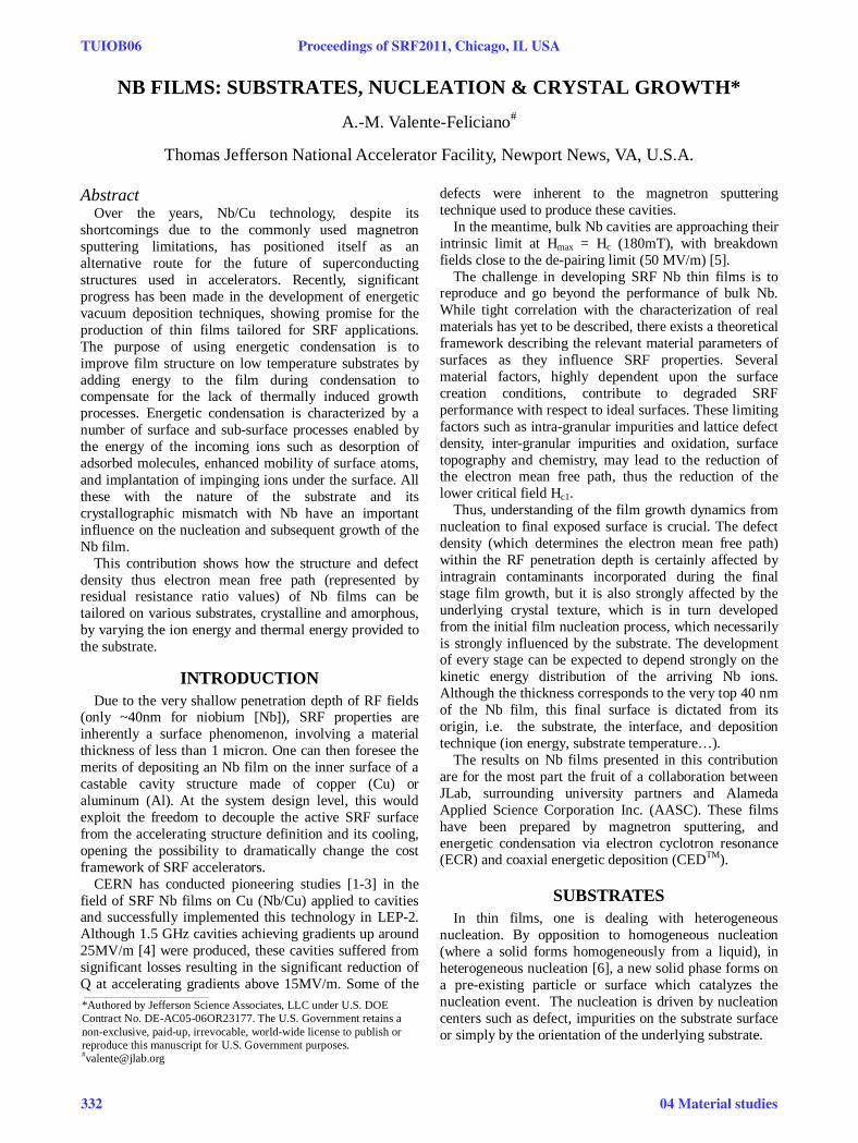
Niobium has established hetero-epitaxial relationships for a variety of materials. Fig. 1 shows the Nb hetero-epitaxial directions for Nb grown on different planes of sapphire (Al2O3) as proposed by Wildes et al. [7].
Table 1 shows the different relationships between Nb and sapphire [7], MgO [8] and Cu [9] substrates.
Lattice mismatch (i.e. the difference in the atom arrangement and spacing between the film and substrate materials) and difference in thermal expansion rate induce strain and stress during film growth. For Al2O3, the lattice mismatch varies from ~1.9% for the a-plane (11-20) to 12% for the c-plane (0001). For example, a-plane sapphire as a substrate is due to the low lattice mismatch (~1.9-12%) and comparable rates of thermal expansion. This makes it a suitable proving ground for niobium thin film studies. In the case of MgO (100), the lattice mismatch is about 10.8%.
Table 1: Hetero-epitaxial relationships between Nb and various single crystal substrates
Substrate material
Substrate orientation
Nb orientation
Sapphire (11-20) (110)
(0001) (111), (110)
MgO (100) (100), (110)
(110) (111)
(111) (110)
Cu (100) (110)
(110) (100)
(111) (110)
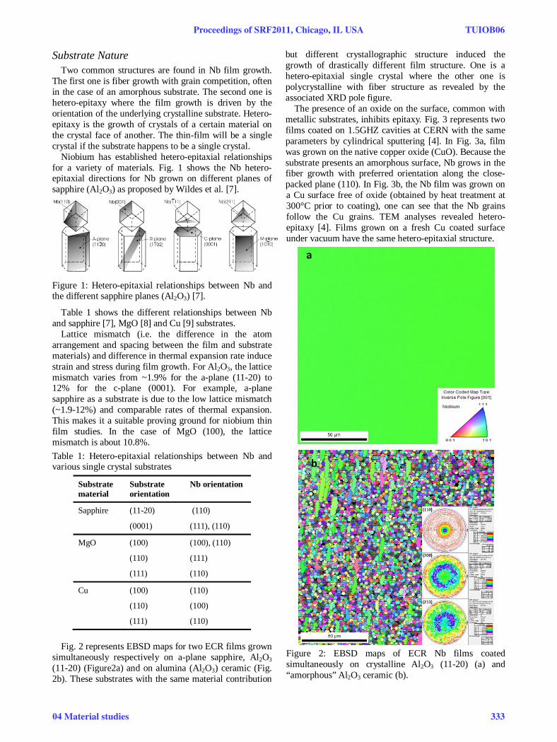
Fig. 2 represents EBSD maps for two ECR films grown
simultaneously respectively on a-plane sapphire, Al2O3 (11-20) (Figure2a) and on alumina (Al2O3) ceramic (Fig. 2b). These substrates with the same material contribution
but different crystallographic structure induced the growth of drastically different film structure. One is a hetero-epitaxial single crystal where the other one is polycrystalline with fiber structure as revealed by the associated XRD pole figure.
The presence of an oxide on the surface, common with metallic substrates, inhibits epitaxy. Fig. 3 represents two films coated on 1.5GHZ cavities at CERN with the same parameters by cylindrical sputtering [4]. In Fig. 3a, film was grown on the native copper oxide (CuO). Because the substrate presents an amorphous surface, Nb grows in the fiber growth with preferred orientation along the close-packed plane (110). In Fig. 3b, the Nb film was grown on a Cu surface free of oxide (obtained by heat treatment at 300°C prior to coating), one can see that the Nb grains follow the Cu grains. TEM analyses revealed hetero-epitaxy [4]. Films grown on a fresh Cu coated surface under vacuum have the same hetero-epitaxial structure.
Figure 2: EBSD maps of ECR Nb films coated simultaneously on crystalline Al2O3 (11-20) (a) and “amorphous” Al2O3 ceramic (b).
Figure 1: Hetero-epitaxial relationships between Nb and the different sapphire planes (Al2O3) [7].
Proceedings of SRF2011, Chicago, IL USA TUIOB06
04 Material studies 333
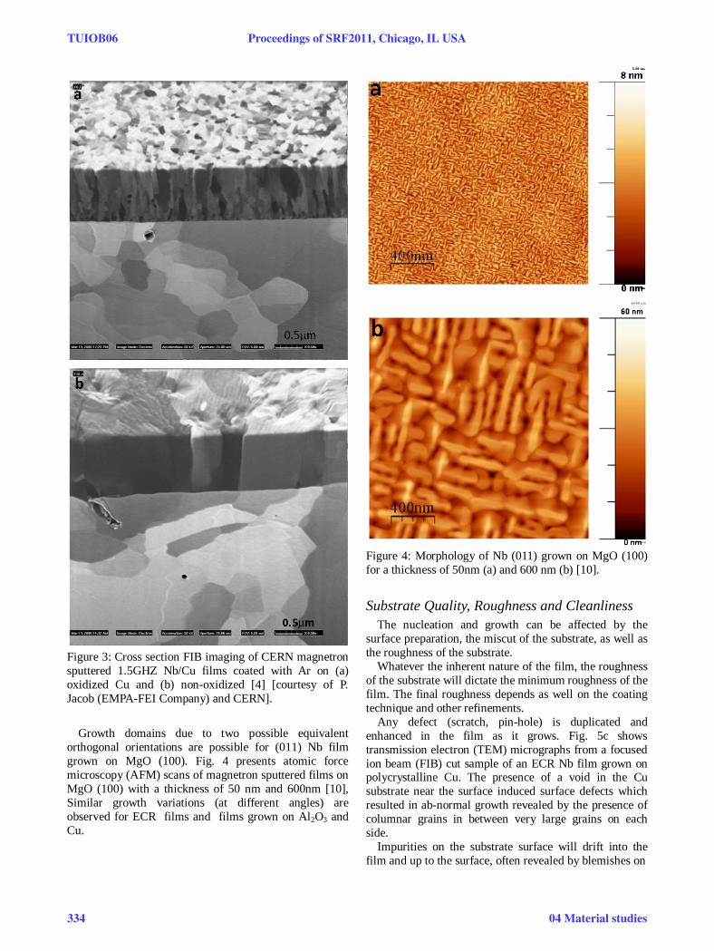
Figure 3: Cross section FIB imaging of CERN magnetron sputtered 1.5GHZ Nb/Cu films coated with Ar on (a) oxidized Cu and (b) non-oxidized [4] [courtesy of P. Jacob (EMPA-FEI Company) and CERN].
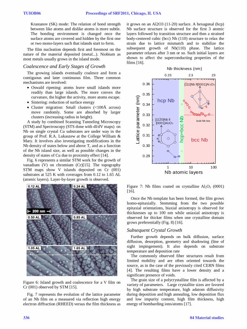
Growth domains due to two possible equivalent
orthogonal orientations are possible for (011) Nb film grown on MgO (100). Fig. 4 presents atomic force microscopy (AFM) scans of magnetron sputtered films on MgO (100) with a thickness of 50 nm and 600nm [10], Similar growth variations (at different angles) are observed for ECR films and films grown on Al2O3 and Cu.
Figure 4: Morphology of Nb (011) grown on MgO (100) for a thickness of 50nm (a) and 600 nm (b) [10].
Substrate Quality, Roughness and Cleanliness
The nucleation and growth can be affected by the surface preparation, the miscut of the substrate, as well as the roughness of the substrate.
Whatever the inherent nature of the film, the roughness of the substrate will dictate the minimum roughness of the film. The final roughness depends as well on the coating technique and other refinements.
Any defect (scratch, pin-hole) is duplicated and enhanced in the film as it grows. Fig. 5c shows transmission electron (TEM) micrographs from a focused ion beam (FIB) cut sample of an ECR Nb film grown on polycrystalline Cu. The presence of a void in the Cu substrate near the surface induced surface defects which resulted in ab-normal growth revealed by the presence of columnar grains in between very large grains on each side.
Impurities on the substrate surface will drift into the film and up to the surface, often revealed by blemishes on
TUIOB06 Proceedings of SRF2011, Chicago, IL USA
334 04 Material studies

the film surface after coating and affecting the final properties of the film. For example two ECR films grown on two MgO (100) substrates side by side varied in RRR from 348 to 156. SIMS data revealed that the H signal was two orders of magnitude higher for the film with the
Tailoring the Interface The interface between substrate and film can be
tailored to promote the desired film growth and properties. Oxides on metallic substrate can be removed to promote hetero-epitaxy: substrate heating [12], surface etching with Ar ions for example. The interface can also be amorphitized to grow independently of the substrate (anodization or modified otherwise). A seed layer can be coated at the interface to favor the growth of a particular structure, minimize the density of grain boundaries [13]. The substrate parameters mentioned such as crystallinity, lattice constant, thermal expansion coefficient, and surface condition (smoothness, purity, surface defects) can bias the crystallinity, orientation, purity and roughness of the resulting film, but they are considered to be second order parameters in film growth, because they are not subject to active control during deposition.
NUCLEATION AND CRYSTAL GROWTH In physical vapor deposition (PVD), thin films grow
from the gas phase. It is a non-equilibrium process phenomenon governed by a competition between kinetics and thermodynamics. The production of Ionic, molecular or atomic species are produced in the gas phase and transported to the substrate. These species then condensate onto the substrate directly (thermal accommodation, binding, surface diffusion) or either by chemical or electrochemical reaction.
Three different regimes can be distinguished in thin film growth: (i) the nucleation and island growth regime, (ii) the island coalescence regime, and (iii) the continuous film regime (subsequent growth).
Nucleation Condensation from the vapor involves incident atoms
becoming bonded adatoms which diffuse over the film surface until they are trapped at low energy lattice sites.
Several competing processes are then at play. The atoms are continuously depositing on the surface. Depending on their energy and the position at which they hit the surface, they can be re-evaporated from the surface, adsorbed (adatom), form a covalent or ionic bond with a surface atom (chemisorption), form a Van der Waal’s bond with a surface atom (physisorption) or migrate on the surface and interact with each other or with the substrate atoms. This atomic odyssey involves four basic processes: shadowing, surface diffusion, bulk diffusion and desorption.
The first three are quantified by the characteristic diffusion and sublimation activation energies (scaling with the melting point). Shadowing arises from the line of sight impingement of arriving toms. The dominance of one or more of these processes as a function of substrate temperature is manifested by different structural morphologies.
In conventional (low energy) PVD, depending on whether or not the bonding between like adatoms is stronger than between adatom and substrate atoms, there are 3 basic growth modes: • 3-D or island growth mode, also known as Volmer–
Weber (VW) mode: The adatoms have a strong affinity with each other and build 3-D islands that grow in all directions, including the direction normal to the surface. The growing islands eventually coalesce and form a contiguous and later continuous film.
• 2-D or layer-by-layer growth, also known as Frank–van der Merwe (FVDM) mode: The condensing particles have a strong affinity for the substrate atoms: they bond to the substrate rather than to each other.
• a mixed mode that starts with 2-D growth that switches into island mode after one or more monolayers; this mode is also known as the Stranski–
Figure 5: (a), SEM micrograph of an ECR Nb/Cu film at the location of FIB cut (b) FIB cross section revealing a void in the Cu substrate near the surface , (c) TEM cross section in dark field revealing the resulting ab-normal growth in the Nb film.
Proceedings of SRF2011, Chicago, IL USA TUIOB06
04 Material studies 335
Krastanov (SK) mode: The relation of bond strength between like atoms and dislike atoms is more subtle. The bonding environment is changed once the surface atoms are covered and hidden by the first one or two mono-layers such that islands start to form.
The film nucleation depends first and foremost on the nature of the material deposited (metal...). Niobium as most metals usually grows in the island mode.
Coalescence and Early Stages of Growth The growing islands eventually coalesce and form a
contiguous and later continuous film. Three common mechanisms are involved:
• Oswald ripening: atoms leave small islands more readily than large islands. The more convex the curvature, the higher the activity, more atoms escape.
• Sintering: reduction of surface energy • Cluster migration: Small clusters (<100Å across)
move randomly. Some are absorbed by larger clusters (increasing radius in height).
A study by combined Scanning Tunneling Microscopy (STM) and Spectroscopy (STS done with dI/dV maps) on Nb on single crystal Cu substrates are under way in the group of Prof. R.A. Lukaszew at the College William & Mary. It involves also investigating modifications in the Nb density of states below and above Tc and as a function of the Nb island size, as well as possible changes in the density of states of Cu due to proximity effect [14].
Fig. 6 represents a similar STM work for the growth of vanadium (V) on chromium (Cr)[15]. The topography STM maps show V islands deposited on Cr (001) substrates at 525 K with coverages from 0.12 to 1.65 AL (atomic layers). Layer-by-layer growth is observed.
Fig. 7 represents the evolution of the lattice parameter of an Nb film on a measured via reflection high energy electron diffraction (RHEED) versus the film thickness as
it grows on an Al2O3 (11-20) surface. A hexagonal (hcp) Nb surface structure is observed for the first 3 atomic layers followed by transition structure and then a strained body-centered cubic (bcc) Nb (110) structure to relax the strain due to lattice mismatch and to stabilize the subsequent growth of Nb(110) phase. The lattice parameter relaxes after 3 nm or so. Such initial layers are shown to affect the superconducting properties of the films [16].
Figure 7: Nb films coated on crystalline Al2O3 (0001) [16].
Once the Nb template has been formed, the film grows homo-epitaxially. Stemming from the two possible epitaxial orientations, biaxial anisotropy is observed for thicknesses up to 100 nm while uniaxial anisotropy is observed for thicker films when one crystalline domain grows preferentially (Fig. 8) [16].
Subsequent Crystal Growth Further growth depends on bulk diffusion, surface
diffusion, desorption, geometry and shadowing (line of sight impingement). It also depends on substrate temperature and deposition rate
The commonly observed fiber structures result from limited mobility and are often oriented towards the source, as in the case of the previously cited CERN films [4]. The resulting films have a lower density and a significant presence of voids.
The grain size of a polycrystalline film is affected by a variety of parameters. Large crystallite sizes are favored by high substrate temperature, high adatom diffusivity during deposition and high annealing, low deposition flux and low impurity content, high film thickness, high energy of bombarding ions/atoms [17].
1 10 100
0.29
0.30
0.31
0.32
0.33
0.34
0.35
0.36
0.23 2.3 23
Nb thickness (nm)
Lat
tice
par
ame
ter
(nm
)
Nb atomic layers
bulk Nb bcc
[111]Nb ll[0001]Al O2 3
[1120]Nb ll [0001]Al O2 3
a
hcp Nb
bcc Nbhcp
+bcc
Nb
a
Figure 6: Island growth and coalescence for a V film on Cr (001) observed by STM [15].
TUIOB06 Proceedings of SRF2011, Chicago, IL USA
336 04 Material studies
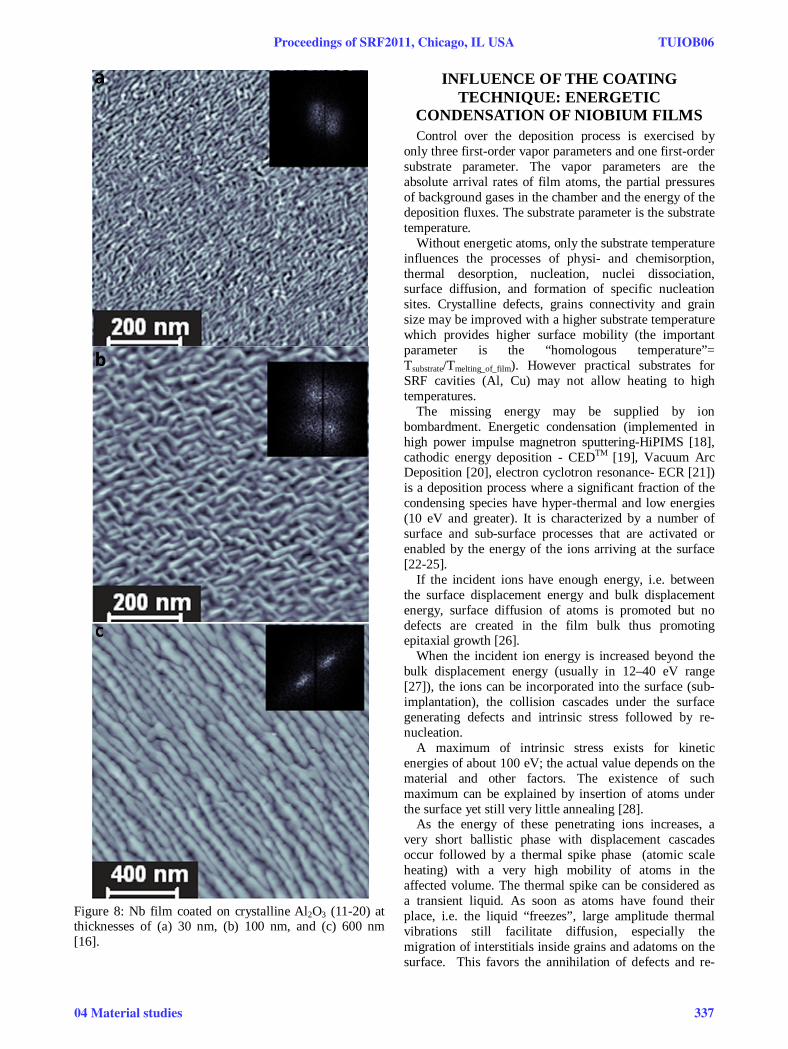
Figure 8: Nb film coated on crystalline Al2O3 (11-20) at thicknesses of (a) 30 nm, (b) 100 nm, and (c) 600 nm [16].
INFLUENCE OF THE COATING TECHNIQUE: ENERGETIC
CONDENSATION OF NIOBIUM FILMS Control over the deposition process is exercised by
only three first-order vapor parameters and one first-order substrate parameter. The vapor parameters are the absolute arrival rates of film atoms, the partial pressures of background gases in the chamber and the energy of the deposition fluxes. The substrate parameter is the substrate temperature.
Without energetic atoms, only the substrate temperature influences the processes of physi- and chemisorption, thermal desorption, nucleation, nuclei dissociation, surface diffusion, and formation of specific nucleation sites. Crystalline defects, grains connectivity and grain size may be improved with a higher substrate temperature which provides higher surface mobility (the important parameter is the “homologous temperature”= Tsubstrate/Tmelting_of_film). However practical substrates for SRF cavities (Al, Cu) may not allow heating to high temperatures.
The missing energy may be supplied by ion bombardment. Energetic condensation (implemented in high power impulse magnetron sputtering-HiPIMS [18], cathodic energy deposition - CEDTM [19], Vacuum Arc Deposition [20], electron cyclotron resonance- ECR [21]) is a deposition process where a significant fraction of the condensing species have hyper-thermal and low energies (10 eV and greater). It is characterized by a number of surface and sub-surface processes that are activated or enabled by the energy of the ions arriving at the surface [22-25].
If the incident ions have enough energy, i.e. between the surface displacement energy and bulk displacement energy, surface diffusion of atoms is promoted but no defects are created in the film bulk thus promoting epitaxial growth [26].
When the incident ion energy is increased beyond the bulk displacement energy (usually in 12–40 eV range [27]), the ions can be incorporated into the surface (sub-implantation), the collision cascades under the surface generating defects and intrinsic stress followed by re-nucleation.
A maximum of intrinsic stress exists for kinetic energies of about 100 eV; the actual value depends on the material and other factors. The existence of such maximum can be explained by insertion of atoms under the surface yet still very little annealing [28].
As the energy of these penetrating ions increases, a very short ballistic phase with displacement cascades occur followed by a thermal spike phase (atomic scale heating) with a very high mobility of atoms in the affected volume. The thermal spike can be considered as a transient liquid. As soon as atoms have found their place, i.e. the liquid “freezes”, large amplitude thermal vibrations still facilitate diffusion, especially the migration of interstitials inside grains and adatoms on the surface. This favors the annihilation of defects and re-
Proceedings of SRF2011, Chicago, IL USA TUIOB06
04 Material studies 337
nucleation. When the majority of condensing species are ions, each of the atoms in the growing film is subject to atomic scale heating several times, namely, once when it arrived and again when neighboring atoms arrived.
As the kinetic ion energy is increased, usually by biasing, the sputtering yield is increased and the net deposition rate is reduced (re-sputtering). Film growth ceases as the average yield approaches unity (between 400 eV and 1400 eV). If the energy is further increased, the surface starts to be etched.
All energy forms brought by particles to the surface will ultimately contribute to broad, non-local heating of the film thus shift the working point of process conditions to higher homologous temperature. This could replace conventional heating and so produce dense films via enhanced surface mobility at generally low bulk temperature. At higher temperature (higher homologous temperature or temperature increase due to the process itself) the grains are enlarged because the increase of ad-atom mobility dominates over the increased ion-bombardment-induced defects and re-nucleation rates [29].
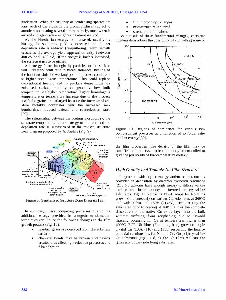
The relationship between the coating morphology, the substrate temperature, kinetic energy of the ions and the deposition rate is summarized in the revised structure zone diagram proposed by A. Anders (Fig. 9).
Figure 9: Generalized Structure Zone Diagram [25].
In summary, these competing processes due to the
additional energy provided in energetic condensation techniques can induce the following changes to the film growth process (Fig. 10):
• residual gases are desorbed from the substrate surface
• chemical bonds may be broken and defects created thus affecting nucleation processes and film adhesion
• film morphology changes • microstructure is altered • stress in the film alters
As a result of these fundamental changes, energetic condensation allows the possibility of controlling some of
the film properties. The density of the film may be modified and the crystal orientation may be controlled to give the possibility of low-temperature epitaxy.
High Quality and Tunable Nb Film Structure In general, with higher energy and/or temperature as
provided in deposition by electron cyclotron resonance [21], Nb adatoms have enough energy to diffuse on the surface and hetero-epitaxy is favored on crystalline substrates. Fig. 11 represents EBSD maps for Nb films grown simultaneously on various Cu substrates at 360°C and with a bias of -150V (214eV). Heat treating the substrates prior to coating at 360°C allows the complete dissolution of the native Cu oxide layer into the bulk without suffering from roughening due to Oswald ripening occurring for Cu at temperatures higher than 400°C. ECR Nb films (Fig. 11 a, b, c) grow on single crystal Cu (100), (110) and (111) respecting the hetero-epitaxial relationships for Nb and Cu. On polycrystalline Cu substrates (Fig. 11 d, e), the Nb films replicate the grain size of the underlying substrates.
Figure 10: Regions of dominance for various ion-bombardment processes as a function of ion/atom ratio and ion energy [30].
TUIOB06 Proceedings of SRF2011, Chicago, IL USA
338 04 Material studies
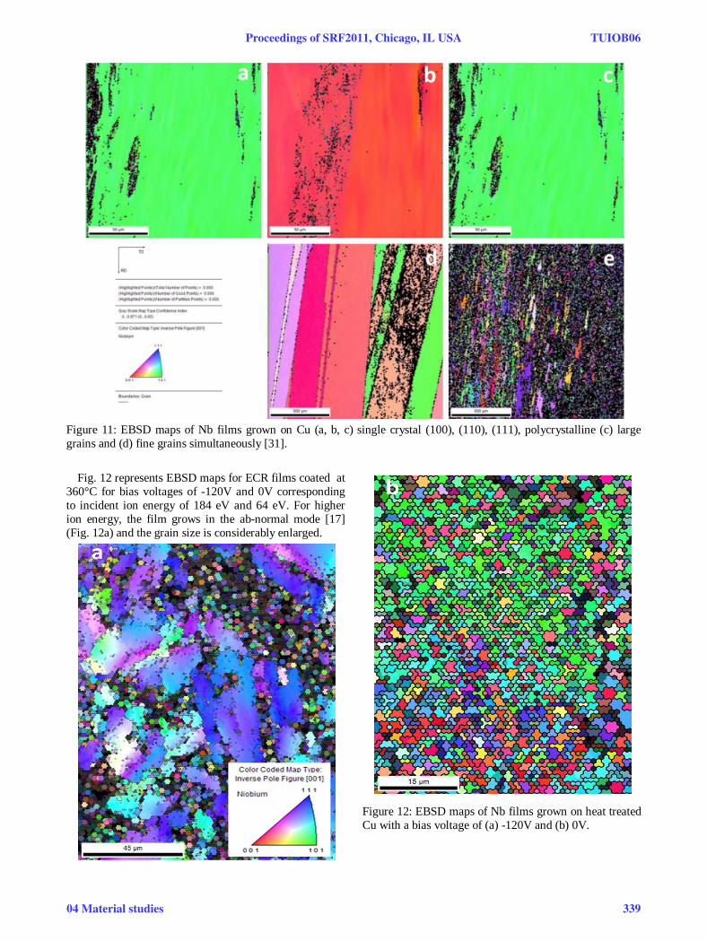
Figure 11: EBSD maps of Nb films grown on Cu (a, b, c) single crystal (100), (110), (111), polycrystalline (c) large grains and (d) fine grains simultaneously [31].
Fig. 12 represents EBSD maps for ECR films coated at
360°C for bias voltages of -120V and 0V corresponding to incident ion energy of 184 eV and 64 eV. For higher ion energy, the film grows in the ab-normal mode [17] (Fig. 12a) and the grain size is considerably enlarged.
Figure 12: EBSD maps of Nb films grown on heat treated Cu with a bias voltage of (a) -120V and (b) 0V.
Proceedings of SRF2011, Chicago, IL USA TUIOB06
04 Material studies 339
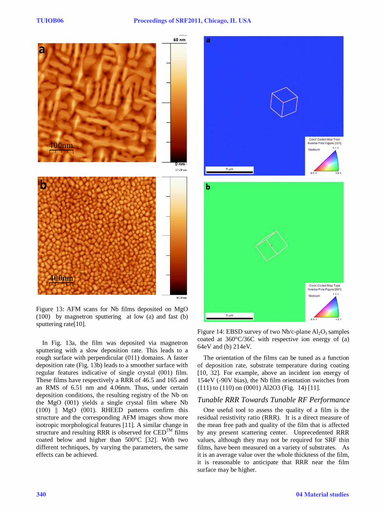
Figure 13: AFM scans for Nb films deposited on MgO (100) by magnetron sputtering at low (a) and fast (b) sputtering rate[10].
In Fig. 13a, the film was deposited via magnetron
sputtering with a slow deposition rate. This leads to a rough surface with perpendicular (011) domains. A faster deposition rate (Fig. 13b) leads to a smoother surface with regular features indicative of single crystal (001) film. These films have respectively a RRR of 46.5 and 165 and an RMS of 6.51 nm and 4.06nm. Thus, under certain deposition conditions, the resulting registry of the Nb on the MgO (001) yields a single crystal film where Nb (100) || MgO (001). RHEED patterns confirm this structure and the corresponding AFM images show more isotropic morphological features [11]. A similar change in structure and resulting RRR is observed for CEDTM films coated below and higher than 500°C [32]. With two different techniques, by varying the parameters, the same effects can be achieved.
Figure 14: EBSD survey of two Nb/c-plane Al2O3 samples coated at 360°C/36C with respective ion energy of (a) 64eV and (b) 214eV.
The orientation of the films can be tuned as a function of deposition rate, substrate temperature during coating [10, 32]. For example, above an incident ion energy of 154eV (-90V bias), the Nb film orientation switches from (111) to (110) on (0001) Al2O3 (Fig. 14) [11].
Tunable RRR Towards Tunable RF Performance One useful tool to assess the quality of a film is the
residual resistivity ratio (RRR). It is a direct measure of the mean free path and quality of the film that is affected by any present scattering center. Unprecedented RRR values, although they may not be required for SRF thin films, have been measured on a variety of substrates. As it is an average value over the whole thickness of the film, it is reasonable to anticipate that RRR near the film surface may be higher.
TUIOB06 Proceedings of SRF2011, Chicago, IL USA
340 04 Material studies
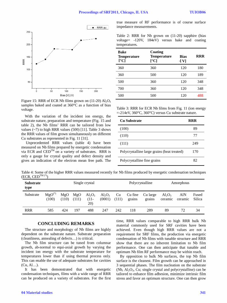
With the variation of the incident ion energy, the substrate nature, preparation and temperature (Fig. 15 and table 2), the Nb films’ RRR can be tailored from low values (~7) to high RRR values (500) [11]. Table 3 shows the RRR values of film grown simultaneously on different Cu substrates as represented in Fig. 11 [31].
Unprecedented RRR values (table 4) have been measured on Nb films prepared by energetic condensation via ECR and CEDTM on a variety of substrates. RRR is only a gauge for crystal quality and defect density and gives an indication of the electron mean free path. The
true measure of RF performance is of course surface impedance measurements.
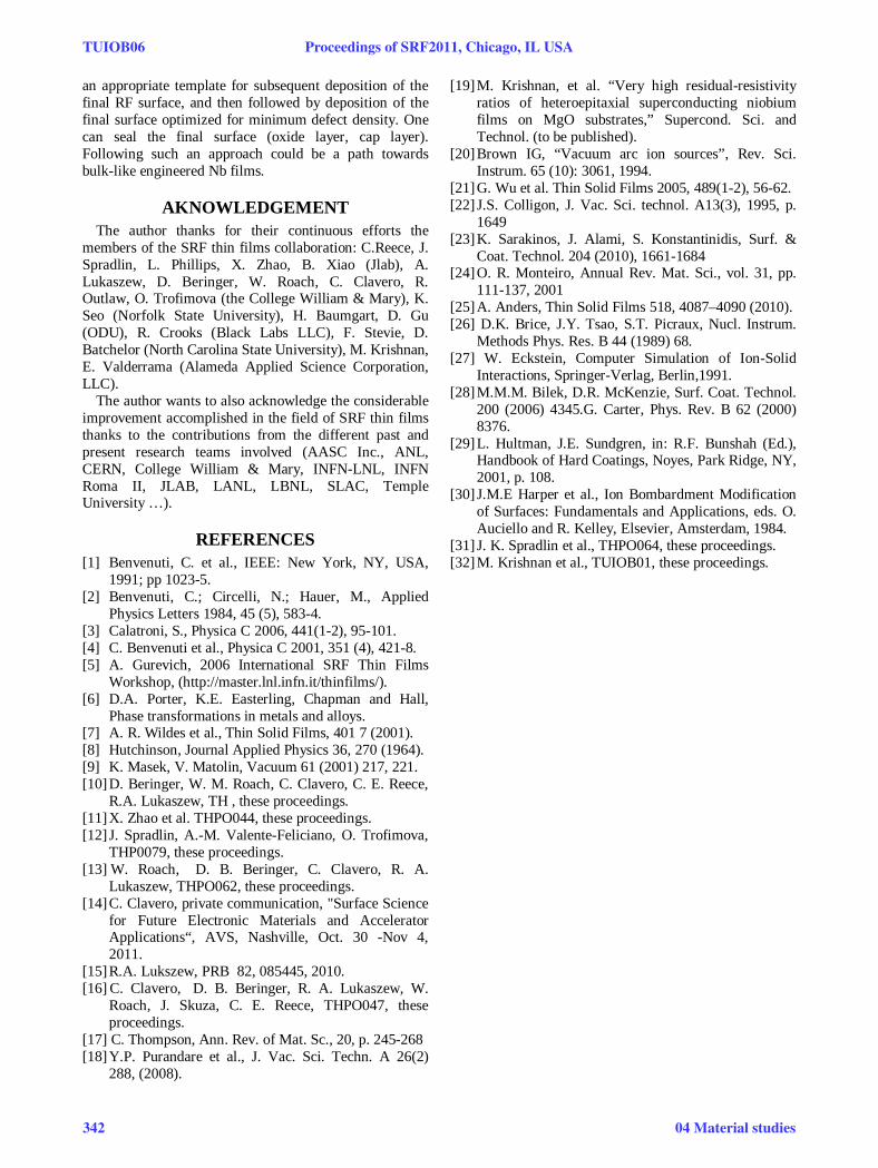
Table 2: RRR for Nb grown on (11-20) sapphire (bias voltage= -120V, 184eV) versus bake and coating temperatures.
Bake Temperature[°C]
Coating Temperature [°C]
Bias[- V]
RRR
360 360 120 180
360 500 120 189
500 360 120 348
700 360 120 348
500 500 120 488
Table 3: RRR for ECR Nb films from Fig. 11 (ion energy =-214eV, 360°C, 360°C) versus Cu substrate nature.
Cu Substrate RRR
(100) 89
(110) 77
(111) 249
Polycrystalline large grains (heat treated) 170
Polycrystalline fine grains 82
Table 4: Some of the higher RRR values measured recently for Nb films produced by energetic condensation techniques (ECR, CEDTM (*))
Substrate type
Single crystal Polycrystalline Amorphous
Substrate MgO(*) (100)
MgO (110)
MgO (111)
Al2O3 (11-20)
Al2O3 (0001)
Cu (111)
Cu fine grains
Cu large grains
Al2O3 ceramic
AlN ceramic
Fused Silica
RRR 585 424 197 488 247 242 118 289 89 72 34
CONCLUDING REMARKS The structure and morphology of Nb films are highly
dependent on the substrate nature. Substrate preparation (cleanliness, annealing of defects…) is critical.
The Nb film structure can be tuned from columnar growth, ab-normal to equi-axial growth by varying the incident ion energy with the substrate temperature for temperatures lower than if using thermal process only. This can enable the use of adequate substrates for cavities (Cu, Al…).
It has been demonstrated that with energetic condensation techniques, films with a wide range of RRR can be produced on a variety of substrates. For the first
time, RRR values comparable to high RRR bulk Nb material commonly used for SRF cavities have been achieved. Even though high RRR values are not a requirement for SRF films, the production via energetic condensation of Nb films with tunable structure and RRR show that there are no inherent limitation to Nb film performance. One can then anticipate that tunable and optimum Nb film RF performance may be within reach.
By opposition to bulk Nb surfaces, the top Nb film surface is the cleanest. Film growth can be approached in 3 sequential phases. The film nucleation on the substrate (Nb, Al2O3, Cu; single crystal and polycrystalline) can be tailored to enhance film adhesion, minimize intrinsic film stress and favor an optimum structure. One can then grow
Figure 15: RRR of ECR Nb films grown on (11-20) Al2O3 samples baked and coated at 360°C as a function of bias voltage.
Proceedings of SRF2011, Chicago, IL USA TUIOB06
04 Material studies 341
an appropriate template for subsequent deposition of the final RF surface, and then followed by deposition of the final surface optimized for minimum defect density. One can seal the final surface (oxide layer, cap layer). Following such an approach could be a path towards bulk-like engineered Nb films.
AKNOWLEDGEMENT The author thanks for their continuous efforts the
members of the SRF thin films collaboration: C.Reece, J. Spradlin, L. Phillips, X. Zhao, B. Xiao (Jlab), A. Lukaszew, D. Beringer, W. Roach, C. Clavero, R. Outlaw, O. Trofimova (the College William & Mary), K. Seo (Norfolk State University), H. Baumgart, D. Gu (ODU), R. Crooks (Black Labs LLC), F. Stevie, D. Batchelor (North Carolina State University), M. Krishnan, E. Valderrama (Alameda Applied Science Corporation, LLC).
The author wants to also acknowledge the considerable improvement accomplished in the field of SRF thin films thanks to the contributions from the different past and present research teams involved (AASC Inc., ANL, CERN, College William & Mary, INFN-LNL, INFN Roma II, JLAB, LANL, LBNL, SLAC, Temple University …).
REFERENCES [1] Benvenuti, C. et al., IEEE: New York, NY, USA,
1991; pp 1023-5. [2] Benvenuti, C.; Circelli, N.; Hauer, M., Applied
Physics Letters 1984, 45 (5), 583-4. [3] Calatroni, S., Physica C 2006, 441(1-2), 95-101. [4] C. Benvenuti et al., Physica C 2001, 351 (4), 421-8. [5] A. Gurevich, 2006 International SRF Thin Films
Workshop, (http://master.lnl.infn.it/thinfilms/). [6] D.A. Porter, K.E. Easterling, Chapman and Hall,
Phase transformations in metals and alloys. [7] A. R. Wildes et al., Thin Solid Films, 401 7 (2001). [8] Hutchinson, Journal Applied Physics 36, 270 (1964). [9] K. Masek, V. Matolin, Vacuum 61 (2001) 217, 221. [10] D. Beringer, W. M. Roach, C. Clavero, C. E. Reece,
R.A. Lukaszew, TH , these proceedings. [11] X. Zhao et al. THPO044, these proceedings. [12] J. Spradlin, A.-M. Valente-Feliciano, O. Trofimova,
THP0079, these proceedings. [13] W. Roach, D. B. Beringer, C. Clavero, R. A.
Lukaszew, THPO062, these proceedings. [14] C. Clavero, private communication, "Surface Science
for Future Electronic Materials and Accelerator Applications“, AVS, Nashville, Oct. 30 -Nov 4, 2011.
[15] R.A. Lukszew, PRB 82, 085445, 2010. [16] C. Clavero, D. B. Beringer, R. A. Lukaszew, W.
Roach, J. Skuza, C. E. Reece, THPO047, these proceedings.
[17] C. Thompson, Ann. Rev. of Mat. Sc., 20, p. 245-268 [18] Y.P. Purandare et al., J. Vac. Sci. Techn. A 26(2)
288, (2008).
[19] M. Krishnan, et al. “Very high residual-resistivity ratios of heteroepitaxial superconducting niobium films on MgO substrates,” Supercond. Sci. and Technol. (to be published).
[20] Brown IG, “Vacuum arc ion sources”, Rev. Sci. Instrum. 65 (10): 3061, 1994.
[21] G. Wu et al. Thin Solid Films 2005, 489(1-2), 56-62. [22] J.S. Colligon, J. Vac. Sci. technol. A13(3), 1995, p.
1649 [23] K. Sarakinos, J. Alami, S. Konstantinidis, Surf. &
Coat. Technol. 204 (2010), 1661-1684 [24] O. R. Monteiro, Annual Rev. Mat. Sci., vol. 31, pp.
111-137, 2001 [25] A. Anders, Thin Solid Films 518, 4087–4090 (2010). [26] D.K. Brice, J.Y. Tsao, S.T. Picraux, Nucl. Instrum.
Methods Phys. Res. B 44 (1989) 68. [27] W. Eckstein, Computer Simulation of Ion-Solid
Interactions, Springer-Verlag, Berlin,1991. [28] M.M.M. Bilek, D.R. McKenzie, Surf. Coat. Technol.
200 (2006) 4345.G. Carter, Phys. Rev. B 62 (2000) 8376.
[29] L. Hultman, J.E. Sundgren, in: R.F. Bunshah (Ed.), Handbook of Hard Coatings, Noyes, Park Ridge, NY, 2001, p. 108.
[30] J.M.E Harper et al., Ion Bombardment Modification of Surfaces: Fundamentals and Applications, eds. O. Auciello and R. Kelley, Elsevier, Amsterdam, 1984.
[31] J. K. Spradlin et al., THPO064, these proceedings. [32] M. Krishnan et al., TUIOB01, these proceedings.
TUIOB06 Proceedings of SRF2011, Chicago, IL USA
342 04 Material studies