naval postgraduate school ticonderoga-class cruiser equipped with an/spy-1 radar ... to null the...
TRANSCRIPT
NAVAL
POSTGRADUATE SCHOOL
MONTEREY, CALIFORNIA
THESIS
Approved for public release; distribution is unlimited
CANCELLATION CIRCUIT FOR TRANSMIT-RECEIVE ISOLATION
by
Wei-Han Cheng
September 2010
Thesis Advisor: David C. Jenn Second Reader: Terry E. Smith

THIS PAGE INTENTIONALLY LEFT BLANK

i
REPORT DOCUMENTATION PAGE Form Approved OMB No. 0704-0188 Public reporting burden for this collection of information is estimated to average 1 hour per response, including the time for reviewing instruction, searching existing data sources, gathering and maintaining the data needed, and completing and reviewing the collection of information. Send comments regarding this burden estimate or any other aspect of this collection of information, including suggestions for reducing this burden, to Washington headquarters Services, Directorate for Information Operations and Reports, 1215 Jefferson Davis Highway, Suite 1204, Arlington, VA 22202-4302, and to the Office of Management and Budget, Paperwork Reduction Project (0704-0188) Washington DC 20503. 1. AGENCY USE ONLY (Leave blank)
2. REPORT DATE September 2010
3. REPORT TYPE AND DATES COVERED Master’s Thesis
4. TITLE AND SUBTITLE Cancellation Circuit for Transmit-Receive Isolation 6. AUTHOR(S) Wei-Han Cheng
5. FUNDING NUMBERS
7. PERFORMING ORGANIZATION NAME(S) AND ADDRESS(ES) Naval Postgraduate School Monterey, CA 93943-5000
8. PERFORMING ORGANIZATION REPORT NUMBER
9. SPONSORING /MONITORING AGENCY NAME(S) AND ADDRESS(ES) N/A
10. SPONSORING/MONITORING AGENCY REPORT NUMBER
11. SUPPLEMENTARY NOTES The views expressed in this thesis are those of the author and do not reflect the official policy or position of the Department of Defense or the U.S. Government. IRB Protocol number ___N/A_.
12a. DISTRIBUTION / AVAILABILITY STATEMENT Approved for public release; distribution is unlimited
12b. DISTRIBUTION CODE
13. ABSTRACT (maximum 200 words) This wireless distributed digital phase array (WDDPA) has been proposed for several military applications in the
sensor and communication areas. The idea of WDDPA is to use a wireless network for transmitting and receiving data between a master controller and modules in an active phased array instead of using a conventional wired beamforming network. The WDDPA provides several advantages over conventional networks such as battlefield survivability, digital architecture and flexibility of system installation on platforms.
A phase synchronization circuit has been developed in the WDDPA application, allowing coherent processing of the data from all elements. There are limitations encountered due to non-ideal hardware, and the performance of the circuit is limited. One of the major problems is the leakage from the circulator. The leakage disrupts the power distributed from the T/R modules. A cancellation circuit has been developed to cancel out the leakage. The performance of the cancellation circuit was investigated by a series of simulations using Agilent ADS (Agilent Advanced Design System), and hardware tests were conducted to characterize the behavior of the circuit. The performance is limited by the accuracy of the attenuator and phase shifter in the cancelation branch. A method for cancelling the residual leakage signal digitally is discussed.
15. NUMBER OF PAGES
83
14. SUBJECT TERMS wireless distributed digital array, wireless beamforming network, transmit/receive module, isolation, leakage cancellation
16. PRICE CODE
17. SECURITY CLASSIFICATION OF REPORT
Unclassified
18. SECURITY CLASSIFICATION OF THIS PAGE
Unclassified
19. SECURITY CLASSIFICATION OF ABSTRACT
Unclassified
20. LIMITATION OF ABSTRACT
UU NSN 7540-01-280-5500 Standard Form 298 (Rev. 2-89) Prescribed by ANSI Std. 239-18

ii
THIS PAGE INTENTIONALLY LEFT BLANK
iii
Approved for public release; distribution is unlimited
CANCELLATION CIRCUIT FOR TRANSMIT-RECEIVE ISOLATION
Wei-Han Cheng Lieutenant, Republic of China Navy
B.S., Virginia Military Institute
Submitted in partial fulfillment of the requirements for the degree of
MASTER OF SCIENCE IN ELECTRONIC WARFARE SYSTEMS ENGINEERING
and
MASTER OF SCIENCE IN ELECTRICAL ENGINEERING
from the
NAVAL POSTGRADUATE SCHOOL September 2010
Author: Wei-Han Cheng
Approved by: David C. Jenn Thesis Advisor
Terry E. Smith Second Reader
R. Clark Robertson Chairman, Department of Electrical and Computer Engineering
Dan C. Boger Chairman, Department of Information Sciences

iv
THIS PAGE INTENTIONALLY LEFT BLANK
v
ABSTRACT
This wireless distributed digital phase array (WDDPA) has been proposed for several
military applications in the sensor and communication areas. The idea of WDDPA is to
use a wireless network for transmitting and receiving data between a master controller
and modules in an active phased array instead of using a conventional wired
beamforming network. The WDDPA provides several advantages over conventional
networks such as battlefield survivability, digital architecture and flexibility of system
installation on platforms.
A phase synchronization circuit has been developed in the WDDPA application,
allowing coherent processing of the data from all elements. There are limitations
encountered due to non-ideal hardware, and the performance of the circuit is limited. One
of the major problems is the leakage from the circulator. The leakage disrupts the power
distributed from the T/R modules. A cancellation circuit has been developed to cancel out
the leakage. The performance of the cancellation circuit was investigated by a series of
simulations using Agilent ADS (Agilent Advanced Design System), and hardware tests
were conducted to characterize the behavior of the circuit. The performance is limited by
the accuracy of the attenuator and phase shifter in the cancelation branch. A method for
cancelling the residual leakage signal digitally is discussed.

vi
THIS PAGE INTENTIONALLY LEFT BLANK
vii
TABLE OF CONTENTS
I. INTRODUCTION........................................................................................................1 A. BACKGROUND ..............................................................................................1 B. OBJECTIVE ....................................................................................................7 C. SCOPE AND ORGANIZATION ...................................................................8
II. SIMULATIONS ...........................................................................................................9 A. BACKGROUND ..............................................................................................9 B. CIRCULATOR LEAKAGE CANCELLATION SIMULATION ............10
1. Background ........................................................................................10 2. Simulation Configuration..................................................................10 3. Simulation Results .............................................................................13
C. ANTENNA MISMATCH SIMULATION...................................................14 1. Background ........................................................................................14 2. Simulation Configuration..................................................................14 3. Simulation Result ...............................................................................15 4. Summary.............................................................................................17
D. MODIFIED TRM SIMULATION ...............................................................17 1. Background ........................................................................................17 2. Simulation Configuration..................................................................18 3. Simulation Result ...............................................................................19
III. HARDWARE TESTING...........................................................................................23 A. LCC HARDWARE TESTING .....................................................................23
1. Background ........................................................................................23 2. Basic Test Configuration...................................................................26 3. LabVIEW Program Development....................................................28 4. Test Results.........................................................................................31 5. Summary.............................................................................................33
B. MODIFIED TRM TEST ...............................................................................33 1. Background ........................................................................................33 2. Modified TRM Test Configuration ..................................................33 3. Phase Mismatch Measurement.........................................................35 4. Summary.............................................................................................35
IV. QUADRATURE DEMODULATOR APPROACH................................................37 A. INTRODUCTION..........................................................................................37 B. DIGITAL CANCELLATION APPROACH...............................................37 C. DEMODULATOR FOR POWER DETECTION IN THE DBFC............41
1. Background ........................................................................................41 2. Quadrature Demodulator Calibration.............................................41 3. Quadrature Demodulator Test .........................................................46 4. Summary.............................................................................................50
D. TEST CIRCUIT DESIGN.............................................................................50

viii
V. SUMMARY, CONCLUSIONS AND RECOMMENDATIONS ...........................57 A. SUMMARY ....................................................................................................57 B. CONCLUSIONS ............................................................................................58 C. RECOMMENDATIONS...............................................................................59
LIST OF REFERENCES......................................................................................................61
INITIAL DISTRIBUTION LIST .........................................................................................63
ix
LIST OF FIGURES
Figure 1. CG-49 Ticonderoga-class cruiser equipped with AN/SPY-1 radar (From [1])......................................................................................................................1
Figure 2. CAD model of Zumwalt-class sized ship with 1200 randomly distributed antenna elements (From [2]). .............................................................................2
Figure 3. Analog BFN (From [3]). ....................................................................................3 Figure 4. Diagram of a WDDPA (From [3]).....................................................................3 Figure 5. DBFC block diagram (From [4]). ......................................................................4 Figure 6. TRM block diagram (After [4]). ........................................................................5 Figure 7. Sequential synchronization illustration..............................................................6 Figure 8. Demonstrated phase comparison algorithm (From [4]).....................................6 Figure 9. A comparison of synchronization data before (red) and after (blue)
incorporating the LCC (From [4]). ....................................................................7 Figure 10. Example of an ADS circuit design schematic....................................................9 Figure 11. Example of a 40 dB sweep in attenuation........................................................10 Figure 12. DBFC simulation configuration.......................................................................11 Figure 13. Operation of the LCC.......................................................................................11 Figure 14. Effect of phase and amplitude imbalance (From [11]). ...................................12 Figure 15. Example of ΔP calculation. .............................................................................14 Figure 16. DBFC with modified antenna configuration....................................................15 Figure 17. Simulation under different load impedances simulating antenna mismatch. ..16 Figure 18. Mismatch tuning simulation result...................................................................17 Figure 19. Modified TRM including propagation path.....................................................18 Figure 20. DBFC and TRM configuration. .......................................................................19 Figure 21. Power received at 50 Ω load. ...........................................................................20 Figure 22. Power from LCC and circulator port 3. ...........................................................20 Figure 23. Cancellation level testing.................................................................................22 Figure 24. NI PXI-1042 system. .......................................................................................23 Figure 25. LabVIEW panel example.................................................................................25 Figure 26. LabVIEW block diagram example. .................................................................26 Figure 27. Basic LCC testing schematic. ..........................................................................28 Figure 28. Power measurement front panel.......................................................................29 Figure 29. Power measurement block diagram. ................................................................29 Figure 30. Mean power measurement front panel.............................................................30 Figure 31. Mean power measurement block diagram. ......................................................31 Figure 32. LCC measured result (with mechanical attenuator).........................................32 Figure 33. LCC measured result (with digital attenuator).................................................32 Figure 34. Modified TRM and DBFC test configuration..................................................34 Figure 35. TRM and DBFC measurements.......................................................................34 Figure 36. TRM phase mismatch measurements. .............................................................35 Figure 37. The in-phase (I) and quadrature (Q) plane (From [12])...................................38 Figure 38. Environment digitization test diagram.............................................................39 Figure 39. DBFC and TRM test diagram. .........................................................................39

x
Figure 40. DBFC and TRM simulation results before and after digital correction...........40 Figure 41. AD8347 demodulator board (From [12]). .......................................................42 Figure 42. Supplementary amplifier board (After [12])....................................................43 Figure 43. Phase and amplitude error (From [12])............................................................43 Figure 44. DC offset error (From [12]). ............................................................................44 Figure 45. Calibration software.........................................................................................45 Figure 46. Calibration station............................................................................................45 Figure 47. Demodulator calibration result. .......................................................................46 Figure 48. Demodulator test configuration. ......................................................................47 Figure 49. Demodulator dynamic range............................................................................48 Figure 50. AD8947 AGC voltage and mixer output level vs. RF input power,
FLO=1900 MHz, FBB=1 MHz, VS=5 V (From [13]). .......................................49 Figure 51. AD8347 demodulator board schematic (From [13]). ......................................49 Figure 52. VGIN voltage curve.........................................................................................50 Figure 53. New DBFC test diagram..................................................................................51 Figure 54. Coupler selection result (X = 3 dB). ................................................................52 Figure 55. Coupler selection result (X = 6 dB). ................................................................53 Figure 56. Coupler selection result (X = 10 dB). ..............................................................53 Figure 57. Coupler selection result (X = 20 dB). ..............................................................54 Figure 58. Finalized DBFC test configurations.................................................................54 Figure 59. Wideband leakage cancellation cicuit using N channels. ................................59 Figure 60. Typical wideband synchronization performance. ............................................59

xi
LIST OF TABLES
Table 1. Difference in power at the load (ΔP) with and without cancellation branch for a source power of -1 dBm. .........................................................................13
Table 2. List of hardware components...........................................................................27 Table 3. AD8347 demodulator specification (From [14]). ............................................42

xii
THIS PAGE INTENTIONALLY LEFT BLANK
xiii
EXECUTIVE SUMMARY
More and more lethal and precise weapons have been developed for modern warfare. For
the Navy, anti-ship missiles are the main threat of the surface warships. These missiles
can be operated in extreme high and low altitudes. They are hard to detect by shipborne
radars. Therefore, phased array radars are typically employed to provide rapid accurate
range and altitude information of targets. The size, weight, and power (SWAP) are radar
system limitations for ships. The conventional beamforming network of phased radars
requires large SWAP to increase angular resolution. A wireless beamforming network
concept was investigated in previous research. In this concept, the conventional
beamforming network is replaced by a wireless network that exchanges data between the
elements and a master controller. A critical aspect of the wireless approach is real-time
synchronization of the elements, which is also accomplised wirelessly. The accuracy of
the wireless synchronization process is limited by the transmit-receive (T/R) isolation at
the master controller. Improving the T/R isolation is the subject of this research.
A prototype wireless beamforming network has been developed. The
synchronization algorithm has also been developed. There are problems, however, that
need to be addressed, such as circulator leakage and mismatch between hardware
components. A leakage cancellation circuit (LCC) is proposed to minimize the effects of
these two problems. The LCC is comprised of a phase shifter and attenuator that are
adjusted to null the leakage and antenna mismatch signals.
Several Agilent ADS (Advanced System Design) simulations were conducted to
examine the behavior of the LCC. From the simulations, it was determined the LCC has
the capability to reduce transmit leakage and improve the performance of the wireless
synchronization process. In addition, a model of a modified transmit-receive module
(TRM) was developed to explore the behavior of the synchronization process. The
modified TRM has an advantage of simplifying simulation for the system and decreasing
the hardware complexity for testing, yet it maintains the required functionality to fully
investigate the leakage effect.

xiv
To validate the simulation results, hardware tests were also conducted. Different
attenuators were bench-tested and compared to examine how the amplitude accuracy
effects cancellation. The modified TRM was built to investigate the performance of the
LCC on the synchronization between the digital beamformer and controller.
In addition to the analog cancellation, a new digital approach was investigated to
improve the synchronization process. Digital cancellation supplements the analog LCC
and could improve the total cancellation. In digital cancellation, a demodulator is
employed to store the residual signal after analog cancellation. Then vector subtraction is
used to eliminate the effect of the residue, which the analog approach cannot suppress.
The LCC was applied successfully to suppress the leakage and mismatches in the
DBFC circuit. The concept of the digital cancellation was validated by a series of
simulations. Among the recommendations for future work is broad banding the analog
cancellation circuit. It is proposed that multiple channels be used in the LCC, each tuned
to a slightly different frequency.
xv
LIST OF ACRONYMS AND ABBREVIATIONS
ADC analog-to-digital converter
ADS Advanced System Design
AGC automatic gain control
ATTEN attenuator
BFN beamforming network
BMD ballistic missile defense
DBFC digital beamformer and controller
DF direction finding
EA electronic attack
EW electronic warfare
LCC leakage cancellation circuit
LNA low noise amplifier
LO local oscillator
NI National Instruments
PA power amplifier
PS phase shifter
RCS radar cross section
SNR signal-to-noise ratio
TRM transmit and receive module
USB Universal Serial Bus
WDDPA wireless distributed digital phase array
WLAN wireless local area network

xvi
THIS PAGE INTENTIONALLY LEFT BLANK

xvii
ACKNOWLEDGMENTS
I would like to express my gratitude to my thesis advisor, Professor David Jenn.
During this research process, he always provided me with helpful suggestions and
directions. Without him, I would not have been able to finish this thesis. Again, it is my
honor to work with Professor Jenn.
I am grateful to my second reader and program officer, Lieutenant Colonel Terry
Smith. He provided me with suggestions and useful information on my courses. Through
these courses, I learned many things which are helpful for my graduate study and future
career.
Many thanks to Microwave Laboratory Director, Mr. Robert Broadston. Every
time I had technical problems, he always assisted me. His enthusiasm and expertise made
me confident during the experiments.
I would like to thank my families. They always gave me support. With their
support, I am able to concentrate on graduate studies and graduate from the Naval
Postgraduate School.
Finally, I also thank the Republic of China Navy for providing this wonderful
opportunity to study at the Naval Postgraduate School.

xviii
THIS PAGE INTENTIONALLY LEFT BLANK
1
I. INTRODUCTION
A. BACKGROUND
Reviewing warfare in recent times, we see that the battle has been transformed
from a conventional war to a high technology war. More and more precise and lethal
weapons have been developed, such as supersonic anti-ship missiles and ballistic missiles,
which can be operated under the extremes of both high or low altitudes with rapid
delivery. They are also hard to detect and track. Technology, however, is a cat and mouse
game. The sensor technology also has taken a great leap forward against those threats.
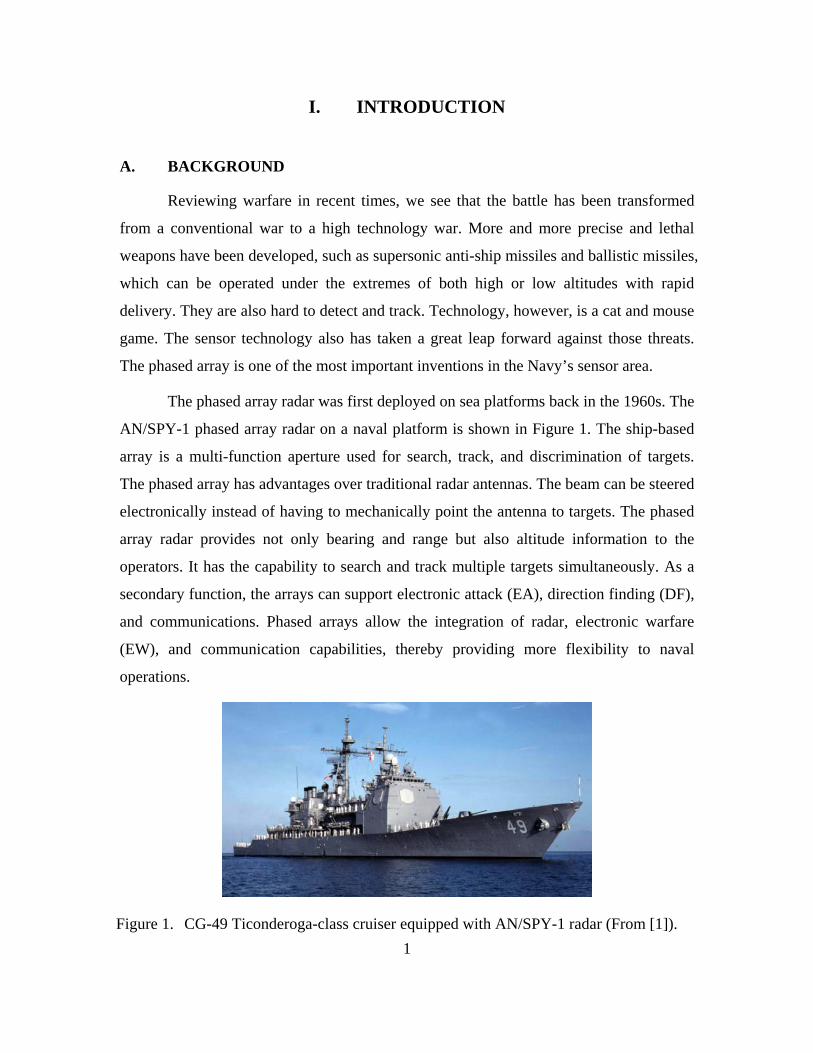
The phased array is one of the most important inventions in the Navy’s sensor area.
The phased array radar was first deployed on sea platforms back in the 1960s. The
AN/SPY-1 phased array radar on a naval platform is shown in Figure 1. The ship-based
array is a multi-function aperture used for search, track, and discrimination of targets.
The phased array has advantages over traditional radar antennas. The beam can be steered
electronically instead of having to mechanically point the antenna to targets. The phased
array radar provides not only bearing and range but also altitude information to the
operators. It has the capability to search and track multiple targets simultaneously. As a
secondary function, the arrays can support electronic attack (EA), direction finding (DF),
and communications. Phased arrays allow the integration of radar, electronic warfare
(EW), and communication capabilities, thereby providing more flexibility to naval
operations.
Figure 1. CG-49 Ticonderoga-class cruiser equipped with AN/SPY-1 radar (From [1]).

2
The phased array, however, has its disadvantages. Phased array antennas require
large areas of the valuable ship surface. To deliver high angular resolution, large arrays
are required. One possible solution to the spatial constraint is using distributed arrays,
which can be spread over the entire ship’s hull. A model of Zumwalt-class sized ship
with 1200 randomly distributed antenna elements is shown in Figure 2. Use of the entire
length of the ship not only increases angular resolution, but also increases the
survivability and decreases the radar cross section (RCS) of ship. In line with this
integrated design philosophy, research into a wireless system approach between arrays
and processors is under way. This exploits today’s state-of-the-art wireless technology.
Figure 2. CAD model of Zumwalt-class sized ship with 1200 randomly distributed antenna elements (From [2]).
Due to the recent improvements in the performance of wireless networks and data
processing, commercial components are now available as candidates for application to
digital phased array systems. Commercial components can decrease the cost of the
system and make the array allocation and deployment on a ship more flexible. The
wireless approach, which is called a wireless distributed digital phase array (WDDPA),
has several advantages over a conventional beamforming network (BFN) or the standard
digital phase array architecture. The WDDPA can be operated in a wider band spectrum
and perform multiple functions. Another advantage is that the survivability of the system
3
is higher when functions are distributed. If one of the components in the network is
disabled, the WDDPA can still be operated in a degraded mode, unlike the conventional
phased array.
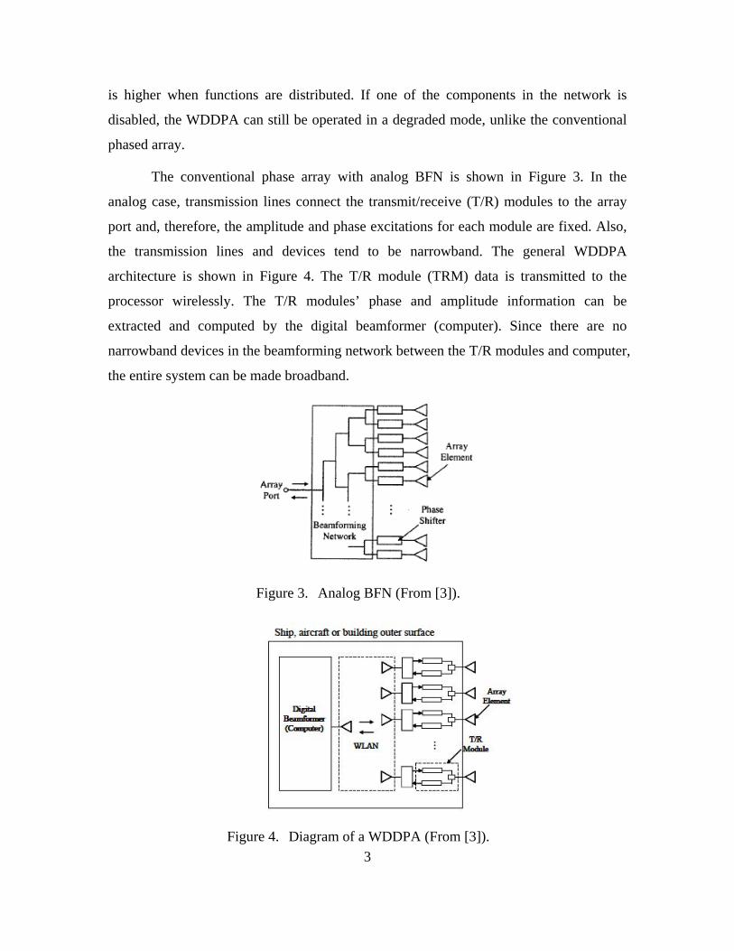
The conventional phase array with analog BFN is shown in Figure 3. In the
analog case, transmission lines connect the transmit/receive (T/R) modules to the array
port and, therefore, the amplitude and phase excitations for each module are fixed. Also,
the transmission lines and devices tend to be narrowband. The general WDDPA
architecture is shown in Figure 4. The T/R module (TRM) data is transmitted to the
processor wirelessly. The T/R modules’ phase and amplitude information can be
extracted and computed by the digital beamformer (computer). Since there are no
narrowband devices in the beamforming network between the T/R modules and computer,
the entire system can be made broadband.
Figure 3. Analog BFN (From [3]).
Figure 4. Diagram of a WDDPA (From [3]).
4
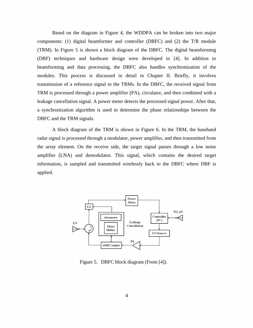
Based on the diagram in Figure 4, the WDDPA can be broken into two major
components: (1) digital beamformer and controller (DBFC) and (2) the T/R module
(TRM). In Figure 5 is shown a block diagram of the DBFC. The digital beamforming
(DBF) techniques and hardware design were developed in [4]. In addition to
beamforming and data processing, the DBFC also handles synchronization of the
modules. This process is discussed in detail in Chapter II. Briefly, it involves
transmission of a reference signal to the TRMs. In the DBFC, the received signal from
TRM is processed through a power amplifier (PA), circulator, and then combined with a
leakage cancellation signal. A power meter detects the processed signal power. After that,
a synchronization algorithm is used to determine the phase relationships between the
DBFC and the TRM signals.
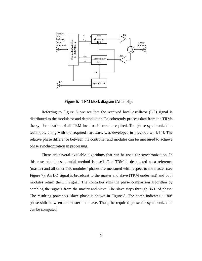
A block diagram of the TRM is shown in Figure 6. In the TRM, the baseband
radar signal is processed through a modulator, power amplifier, and then transmitted from
the array element. On the receive side, the target signal passes through a low noise
amplifier (LNA) and demodulator. This signal, which contains the desired target
information, is sampled and transmitted wirelessly back to the DBFC where DBF is
applied.
Figure 5. DBFC block diagram (From [4]).
5
Figure 6. TRM block diagram (After [4]).
Referring to Figure 6, we see that the received local oscillator (LO) signal is
distributed to the modulator and demodulator. To coherently process data from the TRMs,
the synchronization of all TRM local oscillators is required. The phase synchronization
technique, along with the required hardware, was developed in previous work [4]. The
relative phase difference between the controller and modules can be measured to achieve
phase synchronization in processing.
There are several available algorithms that can be used for synchronization. In
this research, the sequential method is used. One TRM is designated as a reference
(master) and all other T/R modules’ phases are measured with respect to the master (see
Figure 7). An LO signal is broadcast to the master and slave (TRM under test) and both
modules return the LO signal. The controller runs the phase comparison algorithm by
combing the signals from the master and slave. The slave steps through 360° of phase.
The resulting power vs. slave phase is shown in Figure 8. The notch indicates a 180°
phase shift between the master and slave. Thus, the required phase for synchronization
can be computed.

6
Figure 7. Sequential synchronization illustration.
Figure 8. Demonstrated phase comparison algorithm (From [4]).
In practice, there are several problems in implementing the algorithm in hardware.
The leakage power from the circulator degrades the performance of the algorithm by
masking the slave’s returned power and distorts the signal coming from the TRM. There
are different approaches to solve this problem: specific transmitter and receiver designs
[5-6] or adding cancellers [7-10]. In this research, a leakage cancellation circuit (LCC) is
designed to cancel the leakage power from circulator. From the experiment discussed in
[4], it was shown that cancellation can decrease the distortion and improve the

7
performance of the synchronization process. This is evident by a comparison of the
curves in Figure 9. The 6 dB deeper notch allows reception of a weaker desired.
Figure 9. A comparison of synchronization data before (red) and after (blue) incorporating the LCC (From [4]).
B. OBJECTIVE
An effective LCC is required to solve the leakage problem, but the operation of
the LCC is complicated and its performance is a function of many variables. There are
many interactions as well as feedback and coupling mechanisms that potentially affect
the effectiveness of the cancellation channel. Therefore, the objective of this study is to
demonstrate the performance of the LCC and explore ways to improve performance over
a wide range of operating conditions.
Improvement of the LLC is not the only way to enhance the synchronization of
the system. Another possible solution is to increase the dynamic range of the power
detector. If the difference of combined power shown in Figure 8 can be increased, that
would improve the quality of the synchronization between the central controller and the
TRMs over a wider operating range of values.

8
To examine the performance of the candidate designs, simulations were run using
Agilent Advanced Design System (ADS). Several hardware configurations were tested
and the results compared to the simulations.
C. SCOPE AND ORGANIZATION
The basic LCC behavior by using ADS simulations are examined in Chapter II.
The complex interaction between the LCC and the synchronization algorithm can be
understood from the simulations. A simplified model of the TRM is also developed and
tested using ADS. The propagation loss and phase, along with the complicated TRM
response, can be modeled using three components: phase shifter, attenuator, and shorted
termination. These three components can represent a wide range of operating conditions.
Therefore, the behavior of the synchronization process under perfect and imperfect
conditions can be compared.
The experimental testing are examined in Chapter III. Hardware demonstrations
are conducted to compare measured and simulated data. The hardware imperfections and
modifications to the circuit and controller software can be evaluated. The demodulator is
substituted in place of the USB power meter in the DBFC. A comparison between USB
power meter and demodulator measurements is made to see the advantages and
disadvantages of using different detectors.
The possibility of supplementing the analog LCC with digital cancellation is
examined in Chapter IV. Both simulation and measurements are performed. Due to the
nature of demodulators, extra modification of the control pins must be done to measure
the power sensing voltages. If successful, the digital enhancement can potentially add 10
dB more cancellation to the LCC.
The studies and gives suggestions for future research in several critical areas of
WDDPA performance are summarized in Chapter V.
9
II. SIMULATIONS
A. BACKGROUND
Before any hardware experiments were performed, simulations were conducted to
understand the circuit behavior and design parameters. The circuit was simulated using
Agilent Advanced System Design (ADS) software.
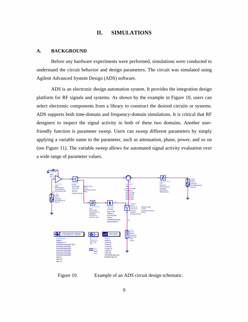
ADS is an electronic design automation system. It provides the integration design
platform for RF signals and systems. As shown by the example in Figure 10, users can
select electronic components from a library to construct the desired circuits or systems.
ADS supports both time-domain and frequency-domain simulations. It is critical that RF
designers to inspect the signal activity in both of these two domains. Another user-
friendly function is parameter sweep. Users can sweep different parameters by simply
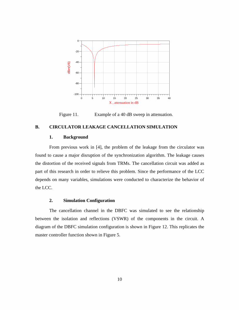
applying a variable name to the parameter, such as attenuation, phase, power, and so on
(see Figure 11). The variable sweep allows for automated signal activity evaluation over
a wide range of parameter values.
Vc
Vt1
V5
V6
ParamSweepSweep1
Step=0.1Stop=40Start=0SimInstanceName[6]=SimInstanceName[5]=SimInstanceName[4]=SimInstanceName[3]=SimInstanceName[2]=SimInstanceName[1]="AC1"SweepVar="X"
PARAMETER SWEEP
PhaseShiftSMLPS4
ZRef=50 OhmRTConj=noFreqStart=PhaseSlope=0.Phase=0
AttenuatorATTEN2
ReturnPhase=0CheckPassivity=yesTemp=Rref=50 OhmVSWR=1Loss=X dB
P_ACPORT3
Freq=2.4Pac=dbmtow(-10)Z=50 OhmNum=3
P_ACPORT2
Freq=2.4Pac=dbmtow(-1)Z=50 OhmNum=2
PwrSplit2PWR2
Delay=CheckPassivity=yesTemp=ZRef=50. Ohm
Isolation=20 dBS22=0.2S11=0.2S31=0.707S21=0.707PhaseShiftSML
PS3
ZRef=50. OhmRTConj=noFreqStart=PhaseSlope=0.Phase=180
PwrSplit2PWR1
Delay=CheckPassivity=yesTemp=ZRef=50. Ohm
Isolation=20 dBS22=0.2S11=0.2S31=0.316S21=0.948
CirculatorCIR2
Z3=50 OhmZ2=50 OhmZ1=50 OhmIsolat=20 dBVSWR1=1Loss1=0.5 dB
TermTerm3
Temp=Vdc=Noise=yesZ=50 OhmNum=3
V_DCSRC2Vdc=14 V
AGC_AmpAMP1
S22=polar(0,180)S11=polar(0,0)ZRef=50 Ohm
OptionsOptions1
MaxWarnings=10GiveAllWarnings=yesI_AbsTol=I_RelTol=V_AbsTol=V_RelTol=Tnom=25Temp=25
OPTIONS
ACAC1
Step=Stop=2.4 GHzStart=2.4 GHzSweepVar="freq"
AC
VARVAR1X=0
EqnVar
Figure 10. Example of an ADS circuit design schematic.
10
5 10 15 20 25 30 350 40
-80
-60
-40
-20
-100
0
X
dBm
(V6)
Figure 11. Example of a 40 dB sweep in attenuation.
B. CIRCULATOR LEAKAGE CANCELLATION SIMULATION
1. Background
From previous work in [4], the problem of the leakage from the circulator was
found to cause a major disruption of the synchronization algorithm. The leakage causes
the distortion of the received signals from TRMs. The cancellation circuit was added as
part of this research in order to relieve this problem. Since the performance of the LCC
depends on many variables, simulations were conducted to characterize the behavior of
the LCC.
2. Simulation Configuration
The cancellation channel in the DBFC was simulated to see the relationship
between the isolation and reflections (VSWR) of the components in the circuit. A
diagram of the DBFC simulation configuration is shown in Figure 12. This replicates the
master controller function shown in Figure 5.
X , attenuation in dB

11
Figure 12. DBFC simulation configuration.
The operation of the LCC is shown in Figure 13. This circuit is located at the
master controller and the source is the master LO broadcast to the TRMs. The arrows
show the major signal flow (multiple reflections are ignored).
Figure 13. Operation of the LCC.
The cancellation signal level (C) is set to cancel the leakage from the circulator
(L). Therefore, the cancellation voltage is equal in amplitude, but opposite in phase to
that of the leakage voltage in the ideal case and, hence, the leakage signal can be
eliminated by the cancellation signal. In terms of complex voltages
( )S L M C S R S+ + − = + ≈ (1)
12
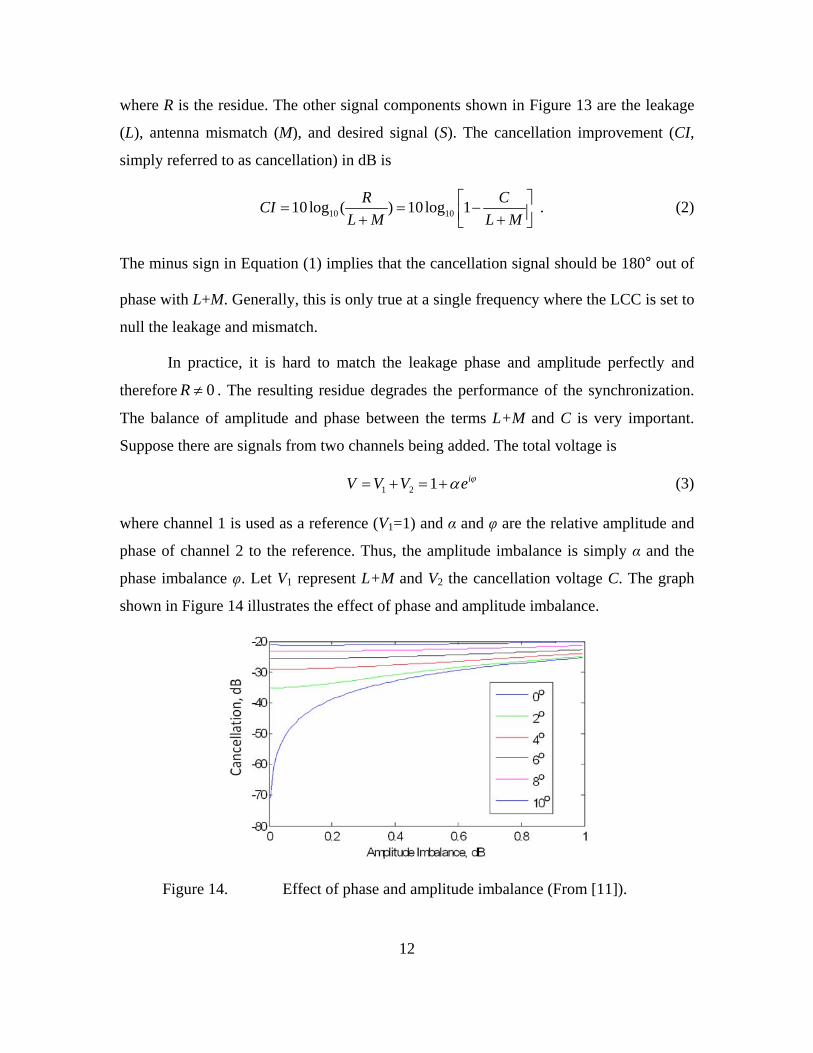
where R is the residue. The other signal components shown in Figure 13 are the leakage
(L), antenna mismatch (M), and desired signal (S). The cancellation improvement (CI,
simply referred to as cancellation) in dB is
10 1010 log ( ) 10log 1R CCIL M L M
⎡ ⎤= = −⎢ ⎥+ +⎣ ⎦ . (2)
The minus sign in Equation (1) implies that the cancellation signal should be 180° out of
phase with L+M. Generally, this is only true at a single frequency where the LCC is set to
null the leakage and mismatch.
In practice, it is hard to match the leakage phase and amplitude perfectly and
therefore 0R ≠ . The resulting residue degrades the performance of the synchronization.
The balance of amplitude and phase between the terms L+M and C is very important.
Suppose there are signals from two channels being added. The total voltage is
1 2 1 iV V V e ϕα= + = + (3)
where channel 1 is used as a reference (V1=1) and α and φ are the relative amplitude and
phase of channel 2 to the reference. Thus, the amplitude imbalance is simply α and the
phase imbalance φ. Let V1 represent L+M and V2 the cancellation voltage C. The graph
shown in Figure 14 illustrates the effect of phase and amplitude imbalance.
Figure 14. Effect of phase and amplitude imbalance (From [11]).

13
From Figure 14, it is clear that even a little difference in the phase and amplitude
can have a big difference on the cancellation level. To achieve a notch depth of 35 to 40
dB, an amplitude balance of ≈ 0.2 dB and phase balance of ≈ 1° are required.
3. Simulation Results
This research first simulates the circuit shown in Figure 12 to see the performance
with and without the cancelation circuit under different device VSWRs, coupler isolation,
and circulator isolation. The isolation parameter of the circulator is set to be 10, 15, and
20 dB. The load impedance at port 2 is set to be 50 Ω, 75 Ω, and 100 Ω. This achieves
VSWRs of 1, 1.5, and 2. The simulated results are presented in Table 1.
Table 1. Difference in power at the load (ΔP) with and without cancellation branch for a source power of -1 dBm.
Isolation 10 dB 15 dB 20 dB
VSWR ΔP (dBm) ΔP (dBm) ΔP (dBm) 1.00 122.97 122.97 122.97 1.50 87.57 87.61 92.65 2.00 82.02 83.74 103.04
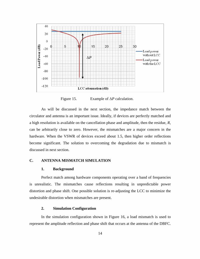
The difference in power at the load (ΔP) with and without the cancellation branch
is defined by
noLCC LCCP P PΔ = − (4)
where PLCC is load power with the LCC and PnoLCC is load power without the LCC. Since
the load is 50 Ω, there is no signal going from circulator port 2 to port 3. This condition is
called the cancellation baseline. Therefore, PnoLCC is simply the leakage from circulator
(L) which is completely negated by the cancellation signal (C) when the attenuation is set
to 10 dB. A graphic view of Equation (4) is shown in Figure 15 (blue line minus red
notch).
14
Figure 15. Example of ΔP calculation.
As will be discussed in the next section, the impedance match between the
circulator and antenna is an important issue. Ideally, if devices are perfectly matched and
a high resolution is available on the cancellation phase and amplitude, then the residue, R,
can be arbitrarily close to zero. However, the mismatches are a major concern in the
hardware. When the VSWR of devices exceed about 1.5, then higher order reflections
become significant. The solution to overcoming the degradation due to mismatch is
discussed in next section.
C. ANTENNA MISMATCH SIMULATION
1. Background
Perfect match among hardware components operating over a band of frequencies
is unrealistic. The mismatches cause reflections resulting in unpredictable power
distortion and phase shift. One possible solution is re-adjusting the LCC to minimize the
undesirable distortion when mismatches are present.
2. Simulation Configuration
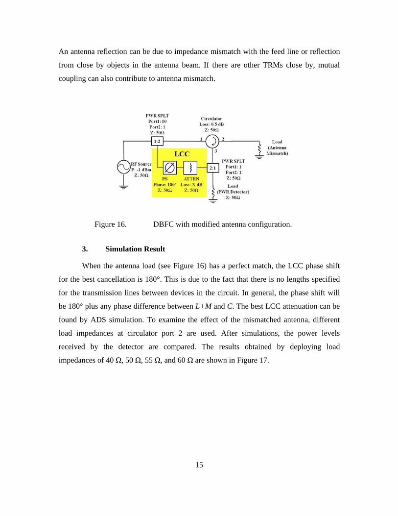
In the simulation configuration shown in Figure 16, a load mismatch is used to
represent the amplitude reflection and phase shift that occurs at the antenna of the DBFC.
ΔP
15
An antenna reflection can be due to impedance mismatch with the feed line or reflection
from close by objects in the antenna beam. If there are other TRMs close by, mutual
coupling can also contribute to antenna mismatch.
Figure 16. DBFC with modified antenna configuration.
3. Simulation Result
When the antenna load (see Figure 16) has a perfect match, the LCC phase shift
for the best cancellation is 180°. This is due to the fact that there is no lengths specified
for the transmission lines between devices in the circuit. In general, the phase shift will
be 180° plus any phase difference between L+M and C. The best LCC attenuation can be
found by ADS simulation. To examine the effect of the mismatched antenna, different
load impedances at circulator port 2 are used. After simulations, the power levels
received by the detector are compared. The results obtained by deploying load
impedances of 40 Ω, 50 Ω, 55 Ω, and 60 Ω are shown in Figure 17.

16
Figure 17. Simulation under different load impedances simulating antenna mismatch.
Referring to Figure 17, we see that a mismatched antenna may cause distortion of
the cancellation signal. The leakage signal level is increased which can mask the desired
signal from TRMs. The impedance mismatch creates reflections and phase shifts that
change L+M. Fortunately, these distortions can be “tuned” by readjusting the LCC.
Therefore, the required LCC attenuation should be re-adjusted as the load impedance gets
larger. By tuning the LCC phase shifter (PS) and attenuator (ATTN), the distortion can be
limited to an acceptable level. The curves shown in Figure 18 are the results before and
after tuning.
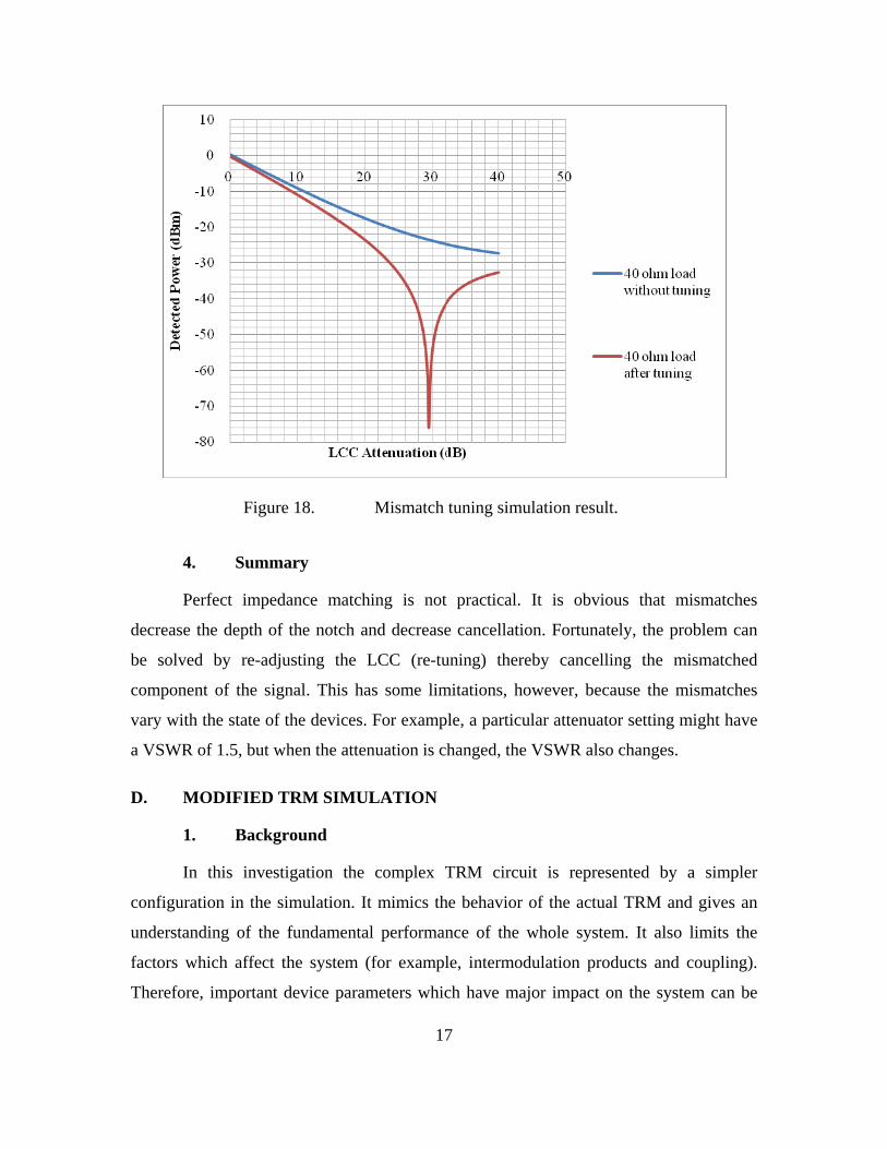
Referring to Figure 18, we see that the blue line is the detected power for a 40 Ω
load when the LCC was tuned for a 50 Ω load. The red line is with re-tuning for the 40 Ω
load. The PS is set to be 0° and the ATTN is re-swept to find the best cancellation. The
tuning successfully drops the notch to -75 dBm.
17
Figure 18. Mismatch tuning simulation result.
4. Summary
Perfect impedance matching is not practical. It is obvious that mismatches
decrease the depth of the notch and decrease cancellation. Fortunately, the problem can
be solved by re-adjusting the LCC (re-tuning) thereby cancelling the mismatched
component of the signal. This has some limitations, however, because the mismatches
vary with the state of the devices. For example, a particular attenuator setting might have
a VSWR of 1.5, but when the attenuation is changed, the VSWR also changes.
D. MODIFIED TRM SIMULATION
1. Background
In this investigation the complex TRM circuit is represented by a simpler
configuration in the simulation. It mimics the behavior of the actual TRM and gives an
understanding of the fundamental performance of the whole system. It also limits the
factors which affect the system (for example, intermodulation products and coupling).
Therefore, important device parameters which have major impact on the system can be

18
studied. The configuration used to represent the TRM and the propagation path between
the controller and TRM is shown in Figure 19.
Figure 19. Modified TRM including propagation path.
In the simplified model, the phase shifter and attenuator are used to control the
round trip attenuation due to path loss. The setting of the attenuator is adjusted to
correspond to the TRM demodulator output power plus any path loss. The phase shifter
can also be used to represent the TRM phase shift applied in the synchronization
procedure.
2. Simulation Configuration
At first the DBFC is simulated to find the best cancelation parameters for the LCC
that provide the maximum leakage cancellation with a 50 Ω load. The best condition was
10.5 dB attenuation and 180° phase shift. The result was a 53.6 dB difference with vs.
without cancellation. This is the best that can be achieved because of the 0.1 dB
attenuator step size. Then, the modified TRM is connected to the DBFC. The TRM
attenuation is swept from 0 dB to 100 dB. It represents the signal from different module
ranges coming to the controller over the entire T/R measurement range. The simulation
configuration is shown in Figure 20.

19
Figure 20. DBFC and TRM configuration.
3. Simulation Result
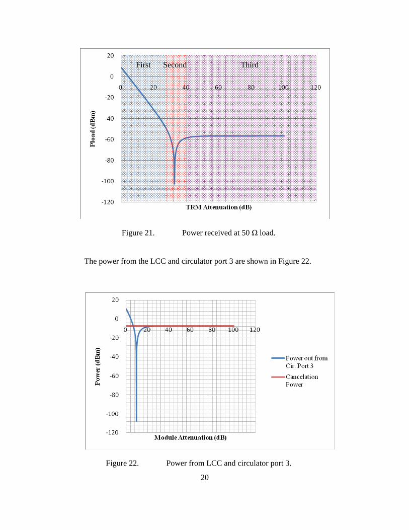
The results in Figure 21 show the power received at the 50 Ω load, which
represents the power (PWR) detector as the TRM attenuator is stepped in 0.1 dB
increments. The first part of the curve (up to about 25 dB) is dominated by the relatively
strong TRM signal, which is decreasing linearly as the attenuation is increased. The
second part is caused by the cancellation of the residue R. The third part (tail) of the
curve is dominated by the residue.
20
Figure 21. Power received at 50 Ω load.
The power from the LCC and circulator port 3 are shown in Figure 22.
Figure 22. Power from LCC and circulator port 3.
First Second Third
21
Ideally, the power received at the power detector (Pload) should decrease linearly
until it reaches -57.3 dBm. It is the deepest notch achieved by the LCC (red curve in
Figure 17). A deeper notch (-105 dBm) occurs, however, that is caused by cancellation of
the residue remaining from the leakage cancellation circuit. The LCC cannot completely
cancel the leakage due to physical limitations on setting the attenuation at 0.25 dB
resolution. Therefore, the leftover power (residue R) can be cancelled by the reflected
power coming back from the TRMs since the attenuator step size of 0.1 dB is less than
the 0.25 dB LCC step size. Thus S cancels the residue R. The notch is made possible by
the fact that the residue is 180° out of phase with the signal S. If the phase is changed
sufficiently, the notch will disappear. This effect also explains the results encountered in
later hardware tests.
From the above discussion, it is evident that the cancellation has a major effect on
the performance of the synchronization process which relies on an accurate measurement
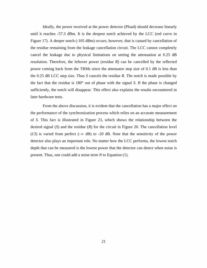
of S. This fact is illustrated in Figure 23, which shows the relationship between the
desired signal (S) and the residue (R) for the circuit in Figure 20. The cancellation level
(CI) is varied from perfect (-∞ dB) to -20 dB. Note that the sensitivity of the power
detector also plays an important role. No matter how the LCC performs, the lowest notch
depth that can be measured is the lowest power that the detector can detect when noise is
present. Thus, one could add a noise term N to Equation (1).
22
Figure 23. Cancellation level testing.
From Figure 23, the cancellation level limits the signal level that can be detected
in the absence of noise. The lowest power that can be detected is based on the residue
after cancellation. Therefore, the precision of cancellation is the key point in determining
the effectiveness of the synchronization process and in-turn the enhancement in the
ability to detect the smallest signals.
In this chapter, the behavior of the LCC and its effect on the DBFC was
investigated. The mismatch of devices plays an important role in the synchronization
performance. The LCC, however, can tune the circuit and minimize the effect of the
leakage and mismatch. It is shown that the LCC improves the performance by allowing
lower desired signal levels to be detected by the power sensor. The next step is to conduct
hardware experiments to verify the simulations.
23
III. HARDWARE TESTING
A. LCC HARDWARE TESTING
1. Background
To demonstrate the effectiveness of the LCC in cancelling leakage as predicted in
the simulations, the DBFC and the LCC were assembled for testing. By measurements
with hardware, the more practical aspects of the problem can be explored.
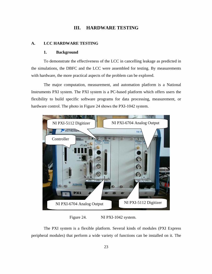
The major computation, measurement, and automation platform is a National
Instruments PXI system. The PXI system is a PC-based platform which offers users the
flexibility to build specific software programs for data processing, measurement, or
hardware control. The photo in Figure 24 shows the PXI-1042 system.
Figure 24. NI PXI-1042 system.
The PXI system is a flexible platform. Several kinds of modules (PXI Express
peripheral modules) that perform a wide variety of functions can be installed on it. The
Controller
NI PXI-5112 Digitizer
NI PXI-6704 Analog Output NI PXI-5112 Digitizer
NI PXI-6704 Analog Output
24
functions and hardware can be expanded. For example, the NI PXI-5112 Digitizer offers
the function of acquiring analog data. The NI-PXIe-5442 Arbitrary Waveform Generator
offers on board waveform-generating capability. Therefore, users can build a
measurement and automation platform suited to their needs.
All processing and device control is accomplished with a single software system,
named LabVIEW. LabVIEW, from National Instruments (NI). It is a graphical
environment programming software. It allows users to develop sophisticated programs
for measurement, control, and testing on PXI platforms. It can also provide data analysis
and visualization. LabVIEW has a large library of functions and toolboxes. Therefore,
many of the system level programs can be quickly built by relatively simple modification
of existing functions. There is also a large “Developer Zone” on the NI web page where
third party software is posted for general use.
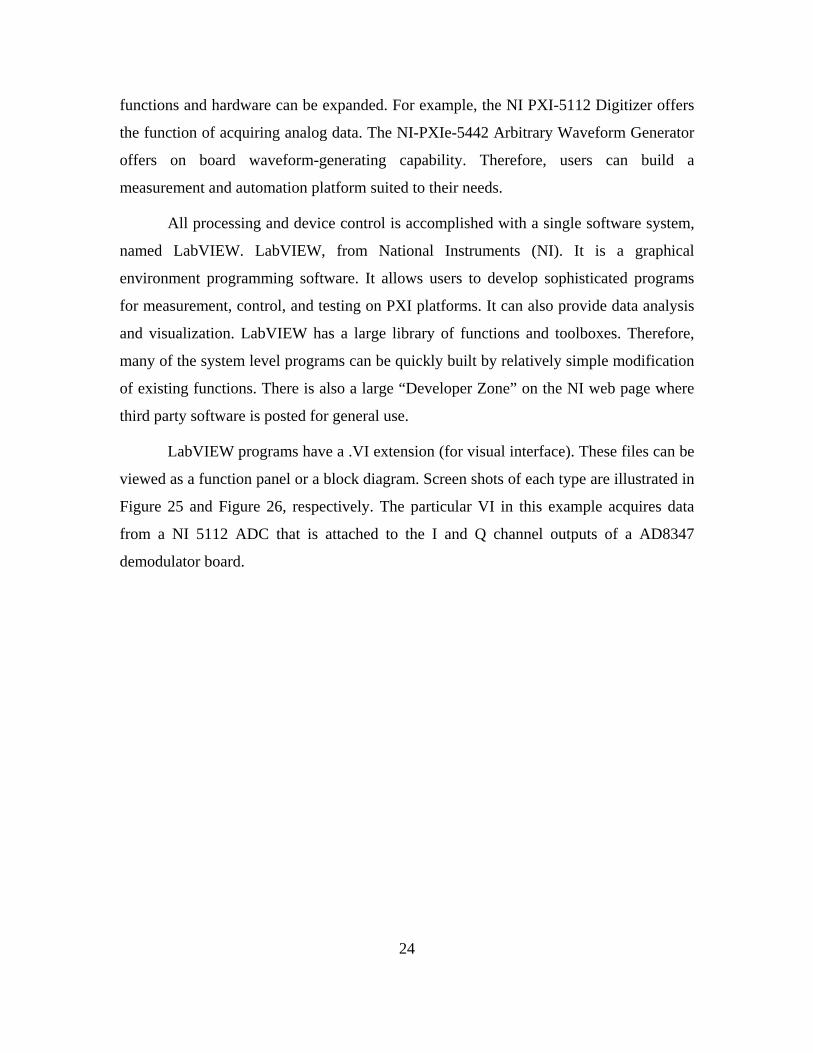
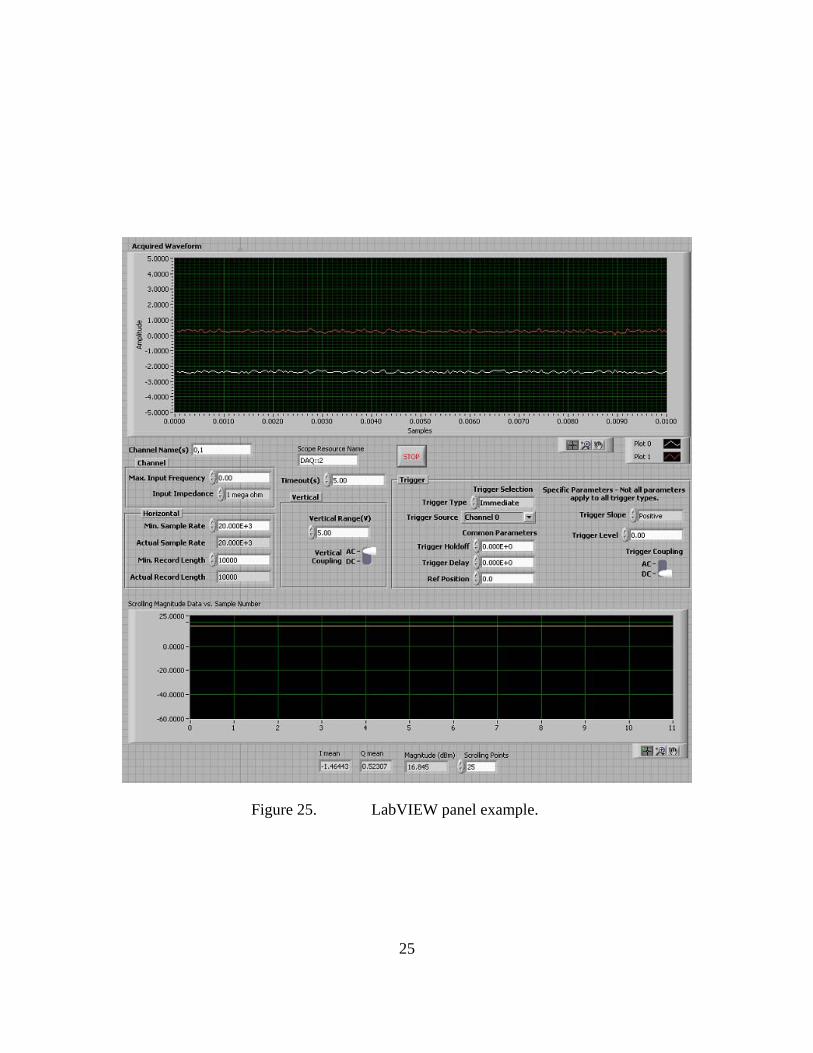
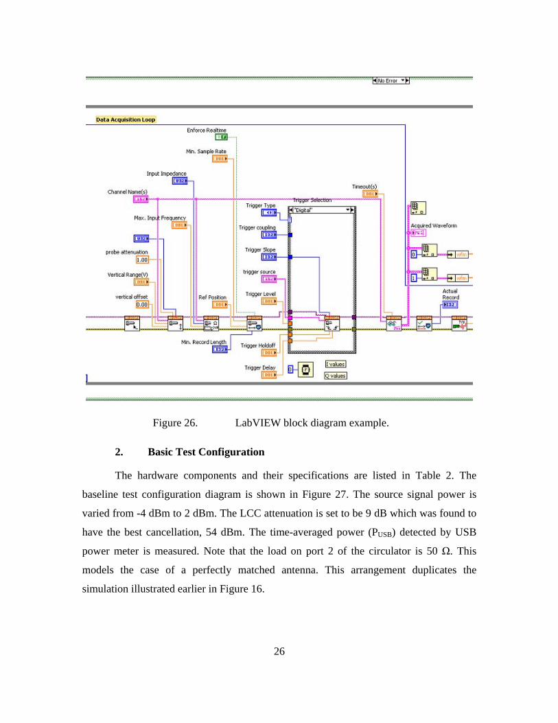
LabVIEW programs have a .VI extension (for visual interface). These files can be
viewed as a function panel or a block diagram. Screen shots of each type are illustrated in
Figure 25 and Figure 26, respectively. The particular VI in this example acquires data
from a NI 5112 ADC that is attached to the I and Q channel outputs of a AD8347
demodulator board.
25
Figure 25. LabVIEW panel example.
26
Figure 26. LabVIEW block diagram example.
2. Basic Test Configuration
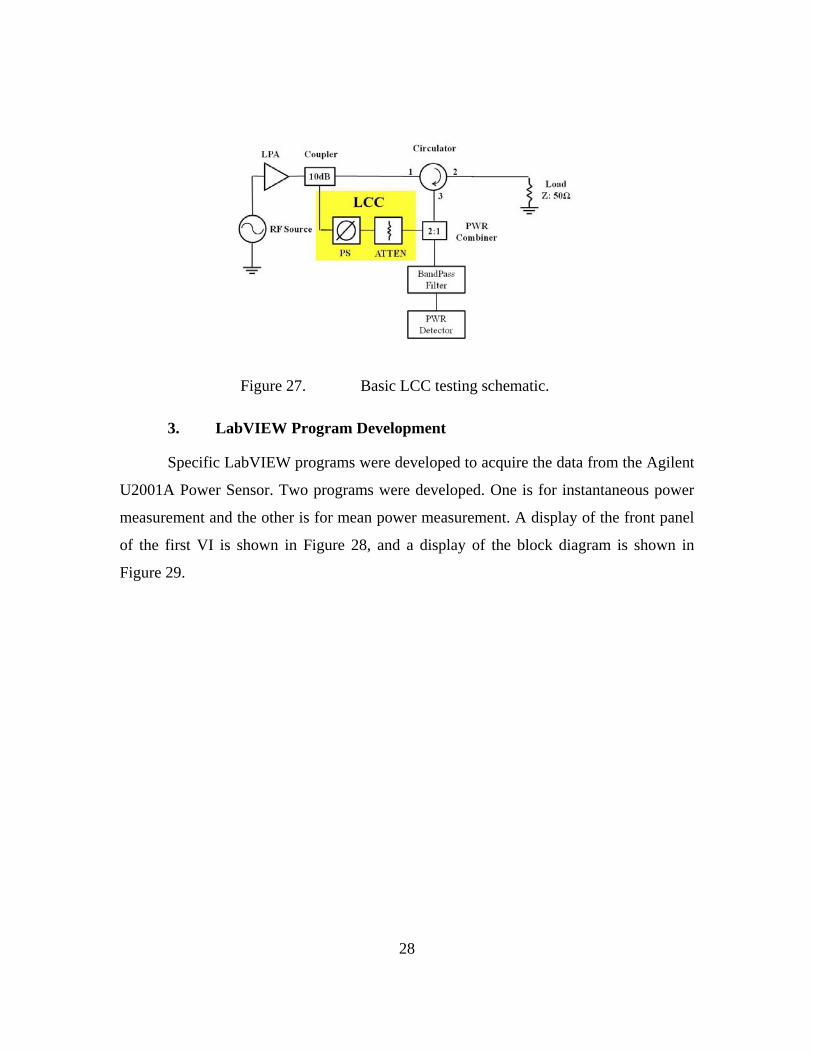
The hardware components and their specifications are listed in Table 2. The
baseline test configuration diagram is shown in Figure 27. The source signal power is
varied from -4 dBm to 2 dBm. The LCC attenuation is set to be 9 dB which was found to
have the best cancellation, 54 dBm. The time-averaged power (PUSB) detected by USB
power meter is measured. Note that the load on port 2 of the circulator is 50 Ω. This
models the case of a perfectly matched antenna. This arrangement duplicates the
simulation illustrated earlier in Figure 16.

27
Table 2. List of hardware components.
Component Manufacturer and Model Specifications
RF Source (RF)
Vaunix Technology LSG–402 Signal Generator
Output power 10 to -40 dBm 100 kHz frequency resolution 55 dB output power control 0.5 dB output power resolution -80 dBc non-harmonic spurious
Low Power Amplifier (LPA)
RF Bay LPA–4–14
Frequency range 10-4000 MHz Gain 18 dB IP3 +34 dBm Noise figure 3.5 dB DC power 12 V SMA connector
3 dB Power Splitter (PWR SPLT)
Pasternack PE2014
Frequency range 2-4 GHz Minimum isolation 20 dB VSWR 1.30 Maximum insertion loss 30 dB SMA female power divider 2 output ports
Circulator DITOM D3C2040
Frequency range 2-4 GHz Impedance 50 Ω Isolation 20 dB Insertion loss 0.4-0.5 dB VSWR 1.25-1.30 AVG power 20 W Peak power 30 W
Phase Shifter (PS)
SAGE LABORATORIES INC. Model 6708
Frequency range DC-8 GHz Phase shift, min 72 °/GHz Insertion phase @ min phase setting 170 °/GHz Number of turns, min 30 VSWRmax 1.60 Insertion loss, max 0.7 dB AVG power 1000 W Peak power 0.45 W Time delay @ min phase setting 3.1 nsec
Mechanical attenuator (ATTN)
JFW INDUSTRIES INC. Model 50R-019 SMA
Frequency range DC-2200 MHz Impedance 50 Ω Attenuation 0-10 dB in 1 dB steps VSWR 1.2 @ DC-1000 MHz VSWR 1.4 @ 1000-2200 MHz Insertion loss 0.2 dB @ DC-1000 MHz Insertion loss 0.4 dB @ 1000-2200 MHz Accuracy ± 0.2 dB @ DC-1000 MHz Accuracy ± 0.4 dB @ 1000-2200 MHz AVG RF input power 2 W Peak RF input power 1000 W
Digital Attenuator (ATTN)
TELEMAKUS LCC TEA4000-7
Frequency range 50 MHz to 4 GHz Attenuation 0-31.75 dB in 0.25 dB steps Interface USB 2.0 Current 150 mA @ 5 V High linearity +59 dBm IP3 P1dB +30 dBm SMA connector
BandPass Filter MFC–13944 Filter
Center frequency 2442 MHz Insertion loss 1.5 dB Relative 3 dB bandwidth 100 MHz Rejection 40 dB @ 2242 MHz Impedance 50 Ω N-female connector
Power Detector Agilent Power Sensor U2001A
Frequency range 10 MHz to 6 GHz Power range -60 to 20 dBm SWRmax 1.15 @ 10-30 MHz SWRmax 1.13 @ 30 MHz to 2 GHz SWRmax 1.19 @ 2-6 GHz Power accuracy ± 4.0%
28
Figure 27. Basic LCC testing schematic.
3. LabVIEW Program Development
Specific LabVIEW programs were developed to acquire the data from the Agilent
U2001A Power Sensor. Two programs were developed. One is for instantaneous power
measurement and the other is for mean power measurement. A display of the front panel
of the first VI is shown in Figure 28, and a display of the block diagram is shown in
Figure 29.
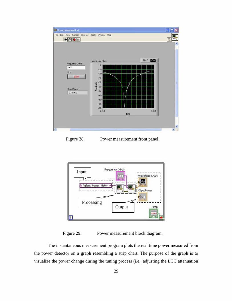
29
Figure 28. Power measurement front panel.
Figure 29. Power measurement block diagram.
The instantaneous measurement program plots the real time power measured from
the power detector on a graph resembling a strip chart. The purpose of the graph is to
visualize the power change during the tuning process (i.e., adjusting the LCC attenuation
Input
Processing Output
30
and phase shift). From the power curve displayed in Figure 28, the tuning of the
cancellation signal amplitude and phase can be observed in real time on the chart. For the
case shown, the residue power level is down to -55 dBm. The program is built with seven
blocks, which are inputs, processing, and output. The two subVI blocks (processing)
acquire the data from the Agilent power meter (input I/O), and present the processed data
in numerical and graphic forms (outputs).
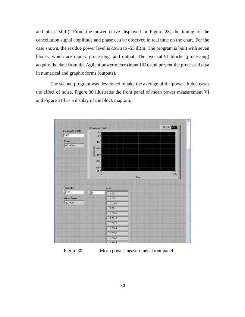
The second program was developed to take the average of the power. It decreases
the effect of noise. Figure 30 illustrates the front panel of mean power measurement VI
and Figure 31 has a display of the block diagram.
Figure 30. Mean power measurement front panel.
31
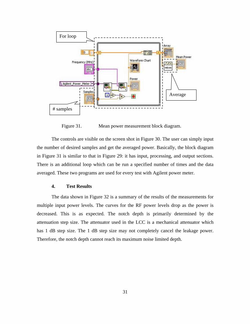
Figure 31. Mean power measurement block diagram.
The controls are visible on the screen shot in Figure 30. The user can simply input
the number of desired samples and get the averaged power. Basically, the block diagram
in Figure 31 is similar to that in Figure 29: it has input, processing, and output sections.
There is an additional loop which can be run a specified number of times and the data
averaged. These two programs are used for every test with Agilent power meter.
4. Test Results
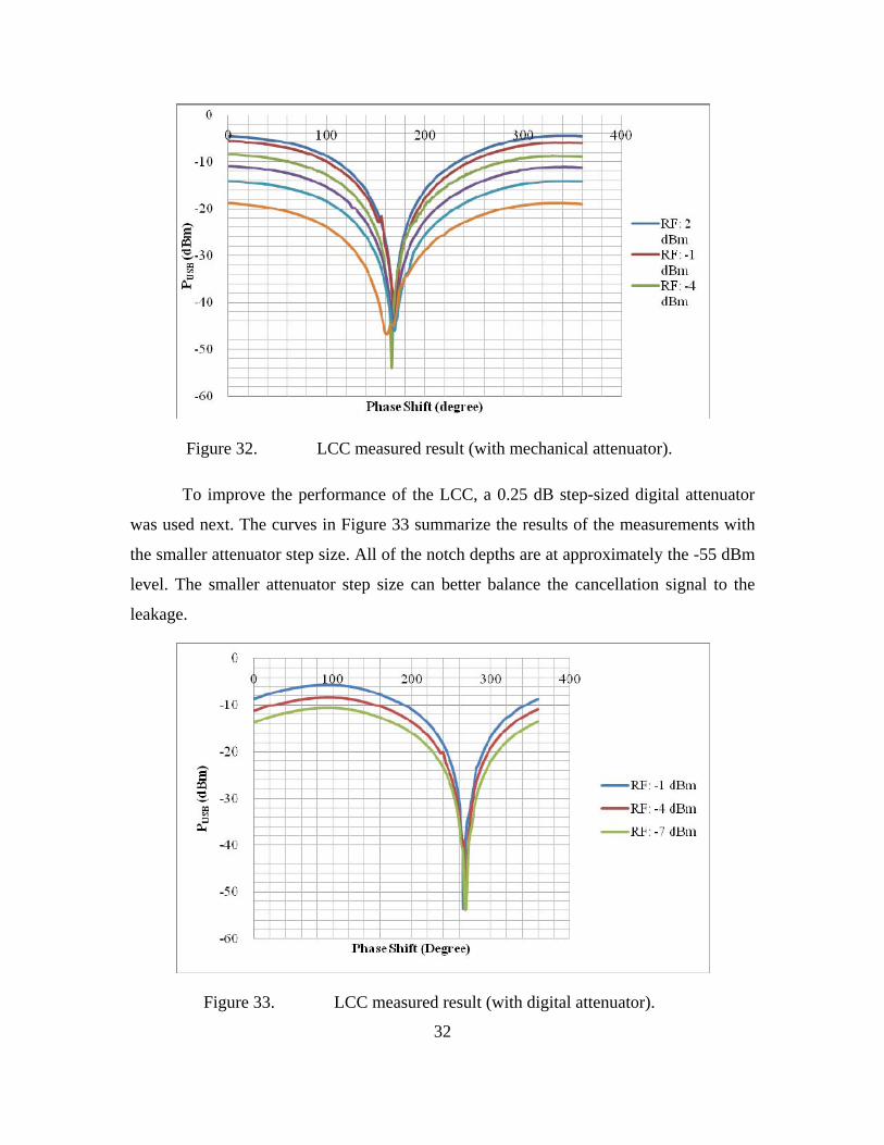
The data shown in Figure 32 is a summary of the results of the measurements for
multiple input power levels. The curves for the RF power levels drop as the power is
decreased. This is as expected. The notch depth is primarily determined by the
attenuation step size. The attenuator used in the LCC is a mechanical attenuator which
has 1 dB step size. The 1 dB step size may not completely cancel the leakage power.
Therefore, the notch depth cannot reach its maximum noise limited depth.
# samples
For loop
Average
32
Figure 32. LCC measured result (with mechanical attenuator).
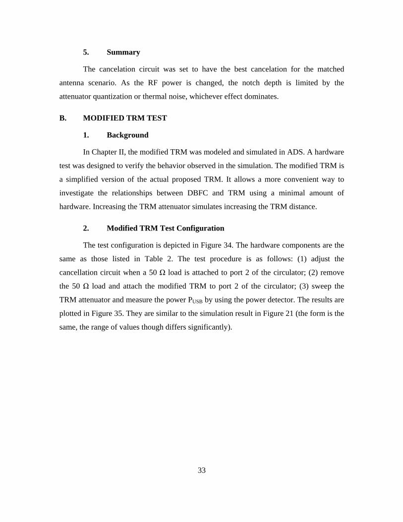
To improve the performance of the LCC, a 0.25 dB step-sized digital attenuator
was used next. The curves in Figure 33 summarize the results of the measurements with
the smaller attenuator step size. All of the notch depths are at approximately the -55 dBm
level. The smaller attenuator step size can better balance the cancellation signal to the
leakage.
Figure 33. LCC measured result (with digital attenuator).
33
5. Summary
The cancelation circuit was set to have the best cancelation for the matched
antenna scenario. As the RF power is changed, the notch depth is limited by the
attenuator quantization or thermal noise, whichever effect dominates.
B. MODIFIED TRM TEST
1. Background
In Chapter II, the modified TRM was modeled and simulated in ADS. A hardware
test was designed to verify the behavior observed in the simulation. The modified TRM is
a simplified version of the actual proposed TRM. It allows a more convenient way to
investigate the relationships between DBFC and TRM using a minimal amount of
hardware. Increasing the TRM attenuator simulates increasing the TRM distance.
2. Modified TRM Test Configuration
The test configuration is depicted in Figure 34. The hardware components are the
same as those listed in Table 2. The test procedure is as follows: (1) adjust the
cancellation circuit when a 50 Ω load is attached to port 2 of the circulator; (2) remove
the 50 Ω load and attach the modified TRM to port 2 of the circulator; (3) sweep the
TRM attenuator and measure the power PUSB by using the power detector. The results are
plotted in Figure 35. They are similar to the simulation result in Figure 21 (the form is the
same, the range of values though differs significantly).

34
Figure 34. Modified TRM and DBFC test configuration.
Figure 35. TRM and DBFC measurements.
First Second Third

35
3. Phase Mismatch Measurement
The measurement PUSB is plotted in Figure 35 for the case of the TRM phase
shifter PS set at 0 phase shift. To see the effect of PS on the cancellation of the residue,
which affects the second region in Figure 35, the TRM PS is set to be 6° and 18°. The RF
power is maintained -1 dBm in these two cases. The results are displayed in Figure 36.
The notch depths of the curves have decreased as predicted by the data in Figure 14.
Figure 36. TRM phase mismatch measurements.
4. Summary
The result follows the simulation results (Figure 21). The first region is dominated
by the signal S and, therefore, it is linear. The linear trend follows the simulated result.
The notch depth in the second region is not as deep as the simulated result. Second, the
flat tail at -15 dBm in the third region is not as low as for the simulation. The level should
be close to the lowest value when the TRM is a 50 Ω load (-54 dBm). The reason may be
the mismatch between circulator and the components of the modified TRM. The multiple
reflections due to different VSWRs create distortion of the signal. The power imbalance
between leakage and the LCC may also introduce the undesirable performance.
First Second Third

36
From Figure 36, the TRM phase shifter PS affects the notch depth of the curves.
Since the residue R is small, it is sensitive to the amplitude and phase. If the cancellation
power is not exactly the same as the residue, it could make a big difference on the notch
depth. The notch depth for a TRM PS of 6° (red) is 15 dB higher than that of TRM PS of
0° (blue). The notch depth for a TRM PS of 18° (green) is 22 dB higher than that of TRM
PS of 0° (blue).
37
IV. QUADRATURE DEMODULATOR APPROACH
A. INTRODUCTION
The previous chapters covered the theory and operation of the LCC as well as
hardware implementation. In practice, the cancellation is limited to about 35 dB due to
phase and amplitude accuracy. Better performance might be achieved by supplementing
the analog cancellation channel with digital cancellation. This chapter describes the
approach and how it would be implemented in hardware.
B. DIGITAL CANCELLATION APPROACH
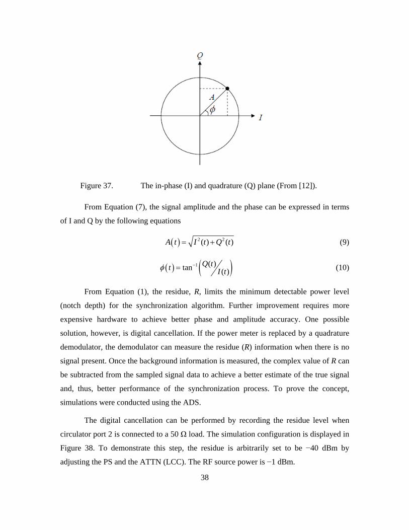
The major advantage of using the demodulator is that its quadrature output retains
the signal phase information. The signals from in-phase (I) and quadrature (Q) channels
can reconstruct the signal’s complex form. The real form of a signal s(t) can be described
as follows
[ ]( ) ( )cos ( ) ( )cs t A t t tω φ= + (5)
where cω = 2 cfπ is the carrier frequency (2.4 GHz in this case) and A(t) is the amplitude
and ( )tφ the phase. Equation (5) can be represented in quadrature form as
( )( ) ( )cos(2 ) ( )sin 2c cs t I t f t Q t f tπ π= − (6)
where
( )( ) cos( ( ))I t A t tφ= (7)
and
( )( ) sin( ( )).Q t A t tφ= (8)
The amplitude and the phase are represented as a point in the I and Q plane which is
shown in Figure 37.
38
Figure 37. The in-phase (I) and quadrature (Q) plane (From [12]).
From Equation (7), the signal amplitude and the phase can be expressed in terms
of I and Q by the following equations
( ) 2 2( ) ( )A t I t Q t= + (9)
( ) ( )1 ( )tan ( )Q tt I tφ −= (10)
From Equation (1), the residue, R, limits the minimum detectable power level
(notch depth) for the synchronization algorithm. Further improvement requires more
expensive hardware to achieve better phase and amplitude accuracy. One possible
solution, however, is digital cancellation. If the power meter is replaced by a quadrature
demodulator, the demodulator can measure the residue (R) information when there is no
signal present. Once the background information is measured, the complex value of R can
be subtracted from the sampled signal data to achieve a better estimate of the true signal
and, thus, better performance of the synchronization process. To prove the concept,
simulations were conducted using the ADS.
The digital cancellation can be performed by recording the residue level when
circulator port 2 is connected to a 50 Ω load. The simulation configuration is displayed in
Figure 38. To demonstrate this step, the residue is arbitrarily set to be −40 dBm by
adjusting the PS and the ATTN (LCC). The RF source power is −1 dBm.
39
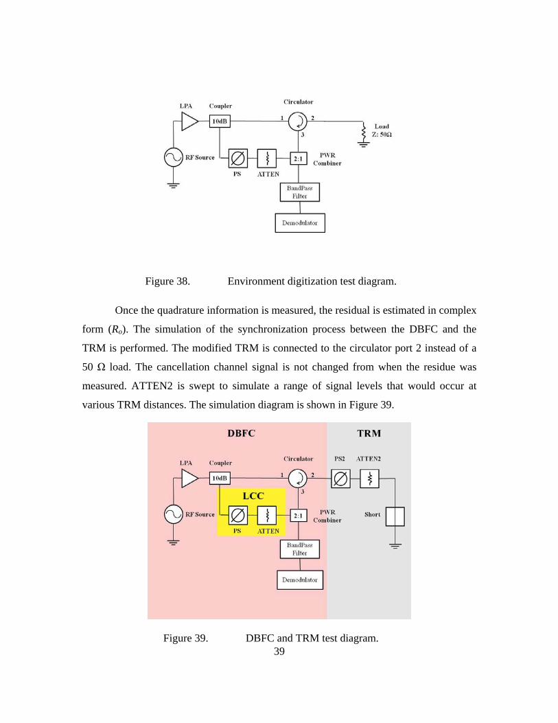
Figure 38. Environment digitization test diagram.
Once the quadrature information is measured, the residual is estimated in complex
form (Ro). The simulation of the synchronization process between the DBFC and the
TRM is performed. The modified TRM is connected to the circulator port 2 instead of a
50 Ω load. The cancellation channel signal is not changed from when the residue was
measured. ATTEN2 is swept to simulate a range of signal levels that would occur at
various TRM distances. The simulation diagram is shown in Figure 39.
Figure 39. DBFC and TRM test diagram.
40
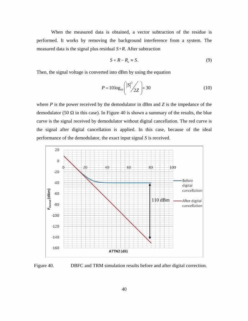
When the measured data is obtained, a vector subtraction of the residue is
performed. It works by removing the background interference from a system. The
measured data is the signal plus residual S+R. After subtraction
.oS R R S+ − ≈ (9)
Then, the signal voltage is converted into dBm by using the equation
2
1010log 302SP Z
⎛ ⎞= +⎜ ⎟⎜ ⎟
⎝ ⎠ (10)
where P is the power received by the demodulator in dBm and Z is the impedance of the
demodulator (50 Ω in this case). In Figure 40 is shown a summary of the results, the blue
curve is the signal received by demodulator without digital cancellation. The red curve is
the signal after digital cancellation is applied. In this case, because of the ideal
performance of the demodulator, the exact input signal S is received.
Figure 40. DBFC and TRM simulation results before and after digital correction.
110 dBm
41
The digital cancellation approach using a demodulator and vector subtraction can
improve the performance of the synchronization algorithm. This resulting curve is linear
if the residue is cancelled perfectly. In practice, the digital improvement will be limited
by the signal-to-noise ratio (SNR) of the I and Q data and quantization error from the
analog-to-digital converter (ADC).
C. DEMODULATOR FOR POWER DETECTION IN THE DBFC
1. Background
From previous test and simulation results, it is known that the LCC and sensitivity
of the power detector plays an important role in the synchronization process. One means
of improvement of the LCC is to deploy digital step attenuators which have a small step
size. This was discussed in Chapter III. In addition, instead of using the power meter, a
quadrature demodulator can possibly be used in the DBFC to improve the sensitivity of
the power measurement. Furthermore, the output has the phase information, which may
allow additional cancellation to be done in the processor using the vector subtraction
method described in Section B.
2. Quadrature Demodulator Calibration
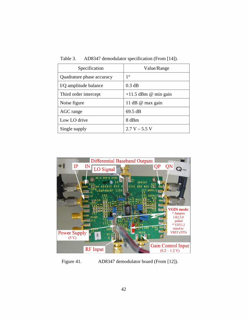
The Analog Devices AD8347 is a Direct Conversion Quadrature Demodulator
(see Figure 41). It has the specifications listed in Table 3. The AD8347 board includes
the quadrature demodulation circuit and integrated RF and baseband amplifiers with
automatic gain control (AGC). A supplementary amplifier board was designed to convert
the differential outputs (I+, I-, Q+, Q-) to single output (I, Q) (see Figure 42). This reduces
the required number of ADCs by half.
42
Table 3. AD8347 demodulator specification (From [14]).
Specification Value/Range
Quadrature phase accuracy 1°
I/Q amplitude balance 0.3 dB
Third order intercept +11.5 dBm @ min gain
Noise figure 11 dB @ max gain
AGC range 69.5 dB
Low LO drive 8 dBm
Single supply 2.7 V – 5.5 V
Figure 41. AD8347 demodulator board (From [12]).

43
Figure 42. Supplementary amplifier board (After [12]).
Each demodulator board has a unique DC offset due to variations in the baseband
circuitry. Before the demodulator is installed in the DBFC, there are some calibration
measurements that need to be done. Many commercial demodulator boards have
problems of DC offset, I/Q mismatch, and even order harmonic distortion. They cause
phase and amplitude errors. Some effects of the phase and amplitude errors are shown in
Figure 43. The effect of DC offset error is shown in Figure 44.
Figure 43. Phase and amplitude error (From [12]).
IP
IN
QP
QN
I Q
44
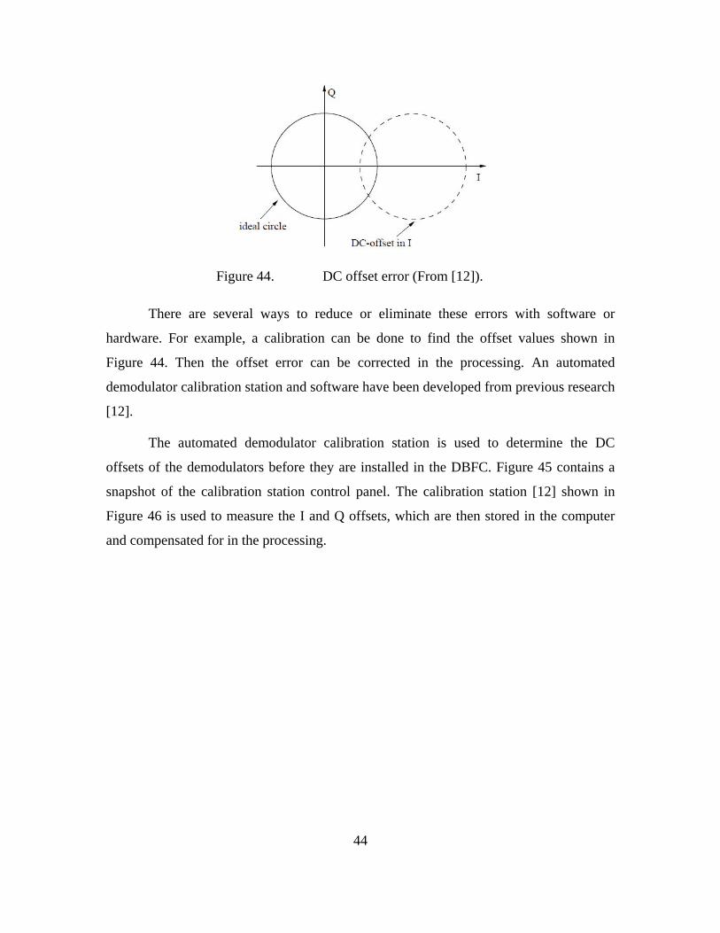
Figure 44. DC offset error (From [12]).
There are several ways to reduce or eliminate these errors with software or
hardware. For example, a calibration can be done to find the offset values shown in
Figure 44. Then the offset error can be corrected in the processing. An automated
demodulator calibration station and software have been developed from previous research
[12].
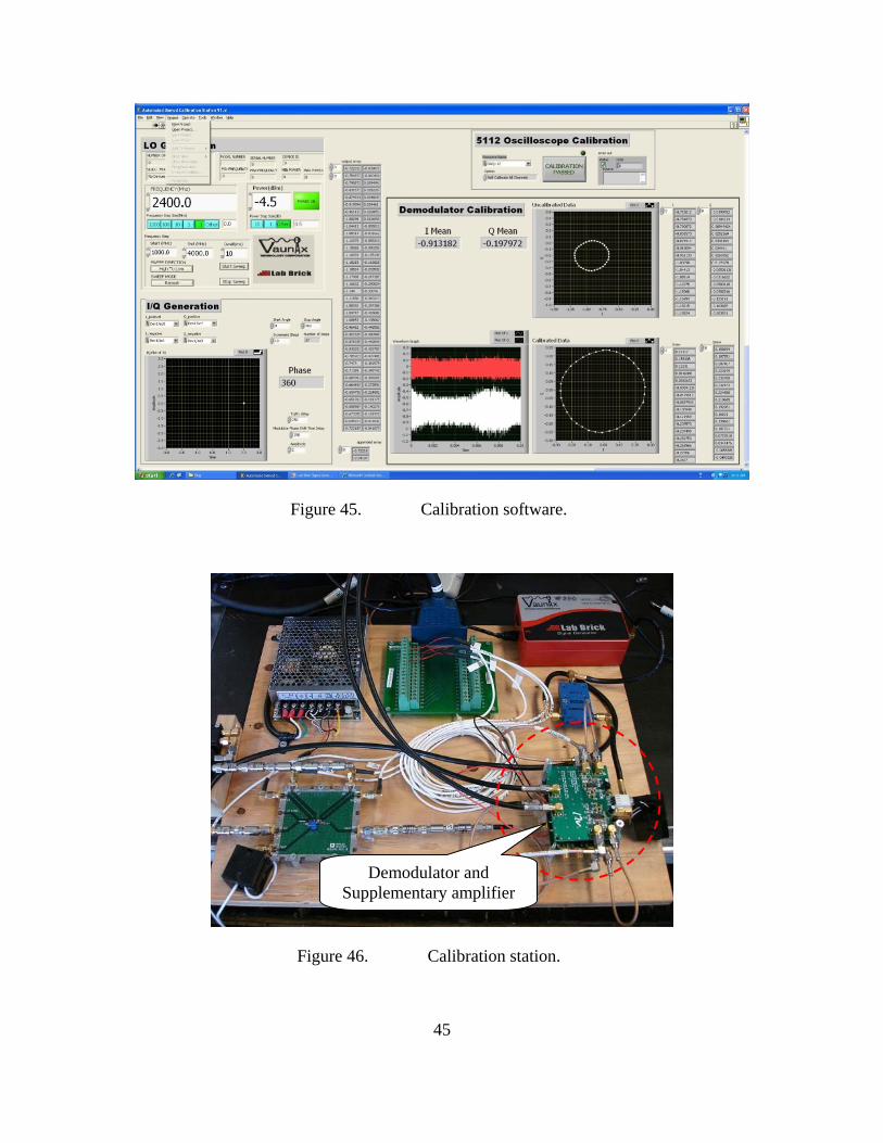
The automated demodulator calibration station is used to determine the DC
offsets of the demodulators before they are installed in the DBFC. Figure 45 contains a
snapshot of the calibration station control panel. The calibration station [12] shown in
Figure 46 is used to measure the I and Q offsets, which are then stored in the computer
and compensated for in the processing.
45
Figure 45. Calibration software.
Figure 46. Calibration station.
Demodulator and Supplementary amplifier

46
The calibration involves sending a 2.4 GHz signal to the demodulator that is
stepped 360° in phase. The I and Q data is plotted and the center recorded as shown in
Figure 47 (top). From the calibration procedure, the offset errors for the demodulator
used in the experiments described in this chapter were found to be -0.913182 V for the I
channel and -0.197972 V for the Q channel. These offsets are used to correct the power
measurement data in subsequent experiments.
Figure 47. Demodulator calibration result.
3. Quadrature Demodulator Test
After the demodulator is calibrated, the sensitivity and the RF dynamic range
were measured for use as a power detector. The power measurement test configuration is
shown in Figure 48. The input RF power varied from −1.5 dBm to −46.5 dBm and the
output voltage computed from the measured I and Q
2 2outV I Q= + . (11)
The time-averaged baseband power out of the demodulator is given by
47
2
2out
outVP Z= . (12)
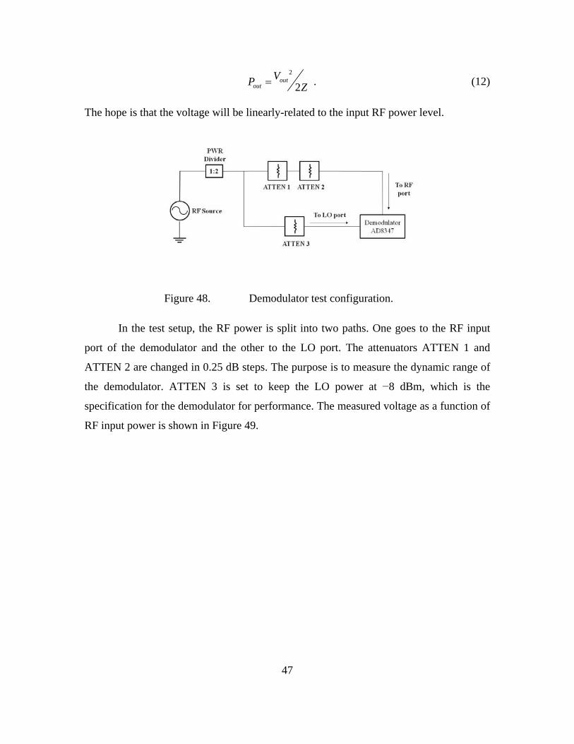
The hope is that the voltage will be linearly-related to the input RF power level.
Figure 48. Demodulator test configuration.
In the test setup, the RF power is split into two paths. One goes to the RF input
port of the demodulator and the other to the LO port. The attenuators ATTEN 1 and
ATTEN 2 are changed in 0.25 dB steps. The purpose is to measure the dynamic range of
the demodulator. ATTEN 3 is set to keep the LO power at −8 dBm, which is the
specification for the demodulator for performance. The measured voltage as a function of
RF input power is shown in Figure 49.
48
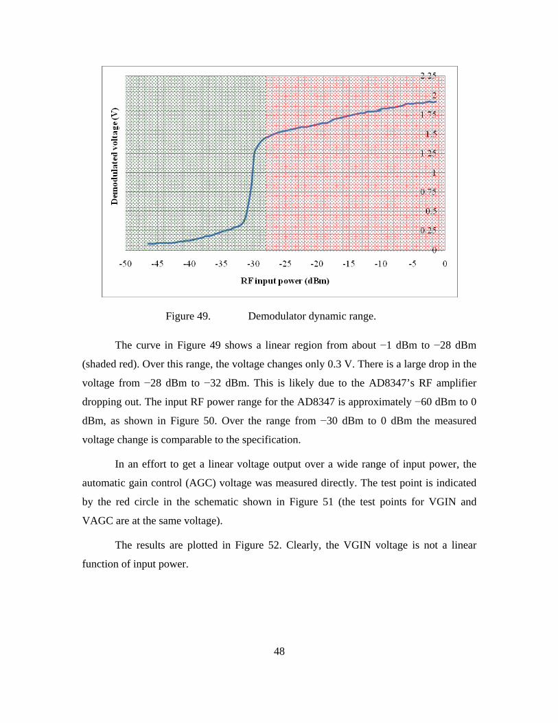
Figure 49. Demodulator dynamic range.
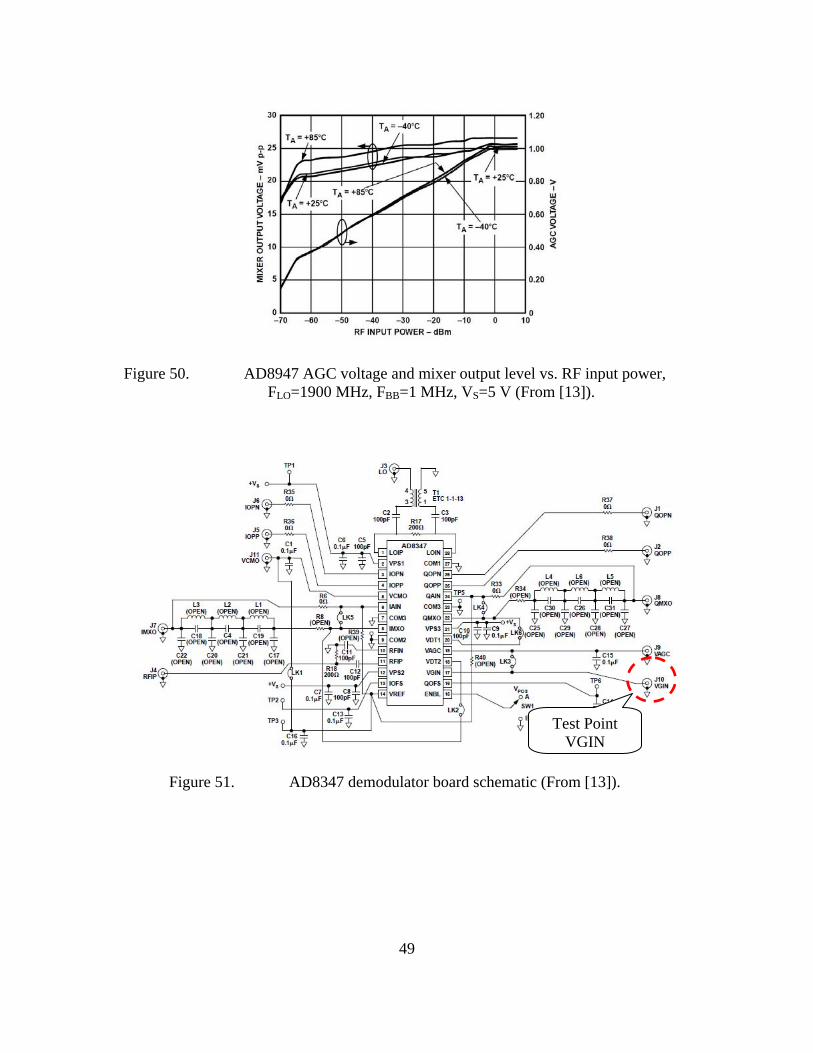
The curve in Figure 49 shows a linear region from about −1 dBm to −28 dBm
(shaded red). Over this range, the voltage changes only 0.3 V. There is a large drop in the
voltage from −28 dBm to −32 dBm. This is likely due to the AD8347’s RF amplifier
dropping out. The input RF power range for the AD8347 is approximately −60 dBm to 0
dBm, as shown in Figure 50. Over the range from −30 dBm to 0 dBm the measured
voltage change is comparable to the specification.
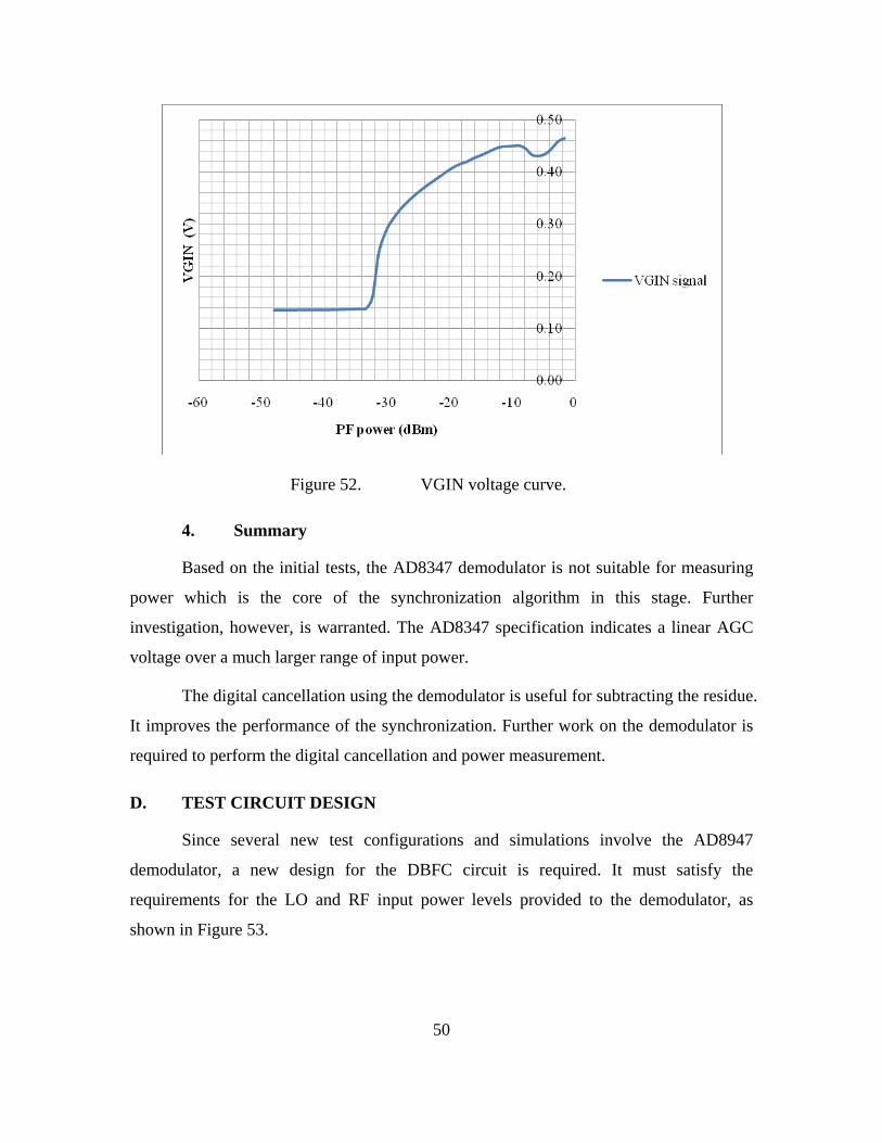
In an effort to get a linear voltage output over a wide range of input power, the
automatic gain control (AGC) voltage was measured directly. The test point is indicated
by the red circle in the schematic shown in Figure 51 (the test points for VGIN and
VAGC are at the same voltage).
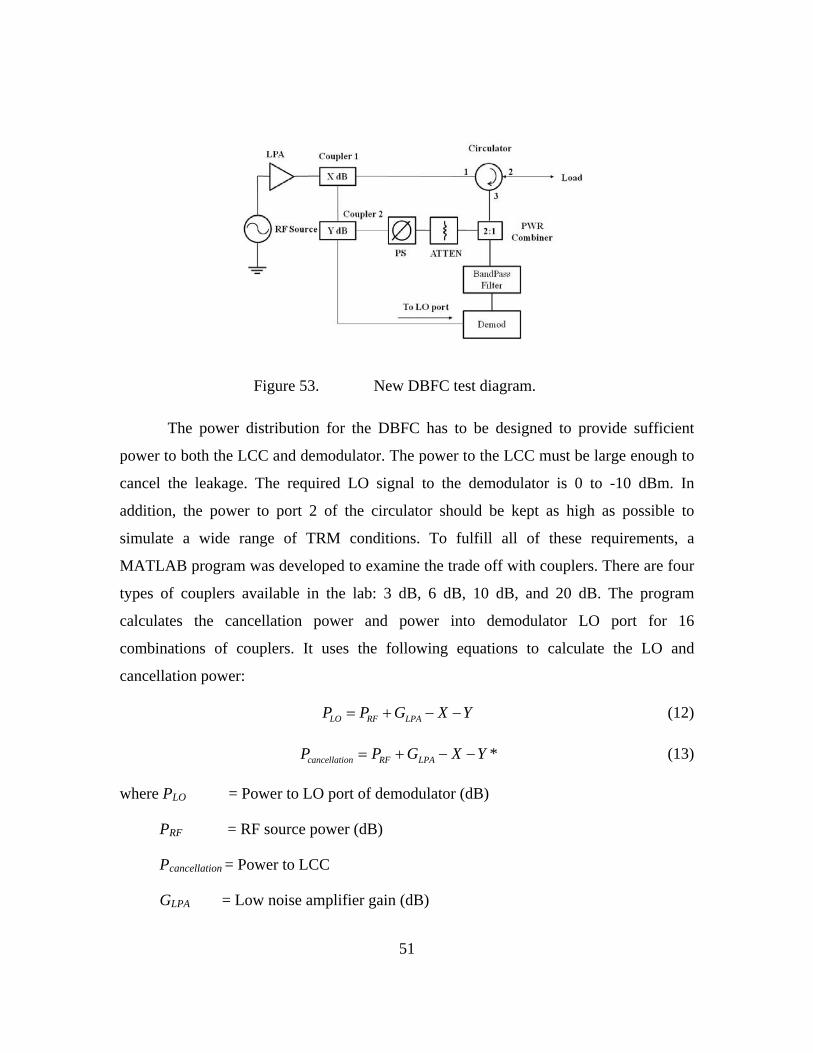
The results are plotted in Figure 52. Clearly, the VGIN voltage is not a linear
function of input power.
49
Figure 50. AD8947 AGC voltage and mixer output level vs. RF input power, FLO=1900 MHz, FBB=1 MHz, VS=5 V (From [13]).
Figure 51. AD8347 demodulator board schematic (From [13]).
Test Point VGIN
50
Figure 52. VGIN voltage curve.
4. Summary
Based on the initial tests, the AD8347 demodulator is not suitable for measuring
power which is the core of the synchronization algorithm in this stage. Further
investigation, however, is warranted. The AD8347 specification indicates a linear AGC
voltage over a much larger range of input power.
The digital cancellation using the demodulator is useful for subtracting the residue.
It improves the performance of the synchronization. Further work on the demodulator is
required to perform the digital cancellation and power measurement.
D. TEST CIRCUIT DESIGN
Since several new test configurations and simulations involve the AD8947
demodulator, a new design for the DBFC circuit is required. It must satisfy the
requirements for the LO and RF input power levels provided to the demodulator, as
shown in Figure 53.
51
Figure 53. New DBFC test diagram.
The power distribution for the DBFC has to be designed to provide sufficient
power to both the LCC and demodulator. The power to the LCC must be large enough to
cancel the leakage. The required LO signal to the demodulator is 0 to -10 dBm. In
addition, the power to port 2 of the circulator should be kept as high as possible to
simulate a wide range of TRM conditions. To fulfill all of these requirements, a
MATLAB program was developed to examine the trade off with couplers. There are four
types of couplers available in the lab: 3 dB, 6 dB, 10 dB, and 20 dB. The program
calculates the cancellation power and power into demodulator LO port for 16
combinations of couplers. It uses the following equations to calculate the LO and
cancellation power:
LO RF LPAP P G X Y= + − − (12)
*cancellation RF LPAP P G X Y= + − − (13)
where PLO = Power to LO port of demodulator (dB)
PRF = RF source power (dB)
Pcancellation = Power to LCC
GLPA = Low noise amplifier gain (dB)

52
X = Coupler 1 coupling (dB)
Y = Coupler 2 coupling at the coupled port (dB)
Y* = Coupler 2 coupling at the output port (dB).
The results are presented in Figure 54 to 57. The notation “3 x 3 LO” denotes PLO with
coupler 1 value (X) by coupler 2 value (Y). The label “C” in the legend represents the
power into the LCC; the label “LO” designates power into the LO.
-50 -40 -30 -20 -10 0 10
-60
-50
-40
-30
-20
-10
0
10
20
30
RF source power (dBm)
Pow
er (d
Bm
)
3X3 LO3X6 LO3X10 LO3X20 LO3X3 C3X6 C3X10 C3X20 C
Figure 54. Coupler selection result (X = 3 dB).

53
-50 -40 -30 -20 -10 0 10
-60
-50
-40
-30
-20
-10
0
10
20
RF source power (dBm)
Pow
er (d
Bm
)
6X3 LO6X6 LO6X10 LO6X20 LO6X3 C6X6 C6X10 C6X20 C
Figure 55. Coupler selection result (X = 6 dB).
-50 -40 -30 -20 -10 0 10
-70
-60
-50
-40
-30
-20
-10
0
10
20
RF source power (dBm)
Pow
er (d
Bm
)
10X3 LO10X6 LO10X10 LO10X20 LO10X3 C10X6 C10X10 C10X20 C
Figure 56. Coupler selection result (X = 10 dB).
54
-50 -40 -30 -20 -10 0 10
-80
-70
-60
-50
-40
-30
-20
-10
0
10
RF source power (dBm)
Pow
er (d
Bm
)
20X3 LO20X6 LO20X10 LO20X20 LO20X3 C20X6 C20X10 C20X20 C
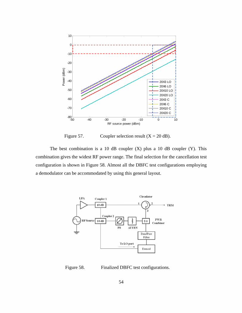
Figure 57. Coupler selection result (X = 20 dB).
The best combination is a 10 dB coupler (X) plus a 10 dB coupler (Y). This
combination gives the widest RF power range. The final selection for the cancellation test
configuration is shown in Figure 58. Almost all the DBFC test configurations employing
a demodulator can be accommodated by using this general layout.
Figure 58. Finalized DBFC test configurations.

55
Some of the hardware issues that arise when the power sensor is replaced by a
quadrature demodulator were examined in this chapter. Further demodulator development
work is required, but the ability of a digital cancelation approach appears promising. A
summary of the research results with conclusions and recommendations is presented in
the next chapter.

56
THIS PAGE INTENTIONALLY LEFT BLANK
57
V. SUMMARY, CONCLUSIONS AND RECOMMENDATIONS
A. SUMMARY
This research focused on the improvement of the WDDPA synchronization circuit
by reducing distortion and errors introduced by leakage and mismatch. The improvement
is primarily achieved by a leakage cancellation circuit (LCC). Several simulations using
ADS and hardware tests with COTS components were conducted to explore the behavior
of the LCC and the AD8347 demodulator in the system.
The cancellation branch of the DBFC circuit has a major effect on the leakage
suppression. If the phase and amplitude are precise enough, the notch depth in the
synchronization power curve shown in Figure 33 can be reduced to allow the detection of
lower signal levels. If the difference between maximum and minimum powers is large
(i.e., large dynamic range), the system can synchronize more accurately. The important
measure of the leakage cancellation is the residue R in Equation (1). The residue
determines the minimum power level that can be received from a TRM during
synchronization. Therefore, to eliminate or reduce the residue to acceptable level is
important for performance improvement. The first step in this direction is to reduce the
step size of the attenuator and phase shifter so that a more accurate balance in amplitude
and phase can be achieved. At some point, however, the synchronization measurement
becomes noise limited. This is because the power detector’s noise will eventually fill the
notch.
An advantage of using the LCC is its “tuning” property. In practice, mismatches
between hardware exist and they are unknown and uncontrollable. The LCC can be
readjusted in the presence of the mismatches. In Figure 18, the two curves show that the
tuning technique can balance the distortion from component mismatch by adjusting
attenuation and phase shift. Unfortunately, the mismatches change with operating
conditions so, to be truly effective, the LCC should be adaptive.
Digital cancellation may provide a significant enhancement to analog cancellation.
It was shown that the complex residue can be stored and a vector subtraction performed
58
on the received signal. Simulations using ADS verify that the digital cancellation
approach is valid. In hardware, the capability to perform the complex measurement of the
residue requires replacing the power meter with a demodulator or other vector voltage
measurement instrument.
An ideal demodulator, such as the one in the ADS device library, provides a
measure of the RF input power from the output I and Q samples, as given in Equation (9).
Therefore, it can be used as a power detector or the output digitized and processed for
digital cancellation. An investigation of the AD8347 demodulator found that the I and Q
outputs gave a linear curve over almost a 27 dB range (Figure 49). The voltage change
over this range was approximately 0.4 V. To increase the dynamic range, an effort was
made to operate the AD8347 without the AGC enabled and use the AGC voltage as a
measure for the input power. This approach was not successful because of the highly
nonlinear behavior of the voltage.
In summary, the LCC was applied successfully to suppress the leakage and
mismatches in the DBFC circuit. The concept of the digital cancellation was validated by
a series of simulations.
B. CONCLUSIONS
The performance of the LCC has been validated by simulations and measurement.
The LCC is effective in reducing leakage and mismatch signals that mask
synchronization signals from the TRMs, thereby allowing the TRMs to operate at larger
ranges, or within the high variations typically seen in the wireless channel environment.
Digital cancellation shows promise in reducing the leakage and mismatch
components even further. The performance, however, of actual COTS demodulators do
not follow what is expected of an ideal quadrature demodulator. Initial measurements on
the AD8347 indicated that the I and Q voltages cannot be used to obtain the amplitude of
the input RF signal. This is likely due to the properties of the baseband amplifier and
automatic gain control circuits integrated with the AD8347.

59
C. RECOMMENDATIONS
There are several areas that merit continued research. One is the need to increase
the bandwidth of the LCC. This can be done by adding more cancellation channels tuned
to slightly different frequencies as depicted in Figure 59. A typical output using three
channels is shown in Figure 60. The approach can be simulated in ADS as a first step
before hardware is assembled and tested.
Figure 59. Wideband leakage cancellation cicuit using N channels.
Figure 60. Typical wideband synchronization performance.

60
Further investigation of the AD8347 demodulator is warranted. If a work-around
for the AGC problem can be found, then hardware validation of the digital cancellation
method can proceed.
61
LIST OF REFERENCES
[1] Jane’s Defense Equipment Image Library, “CG-49 Vincennes, Ticonderoga class cruiser,” date posted: 05 August 2008.
[2] C. H. Tong, “System study and design of broad-band U-slot microstrip patch antennas for aperstuctures and opportunistic arrays,” Naval Postgraduate School Master’s Thesis, Monterey, California, December 2005.
[3] D. C. Jenn, Program review, “Wirelessly Networked Aperstructure Digital Phased Array,” Naval Postgraduate School, May 2007 (unpublished).
[4] Tsai, Yen-Chang, “Development of the phase synchronization circuit for wirelessly distributed digital phased array,” Naval Postgraduate School Master’s Thesis, September 2009.
[5] M. Secmen, S. Demir and A. Hizal, “Dual-polarised T/R Antenna System Suitable for FMCW Altimeter Radar Applications,” IEE Proc. Microw. Antennas & Propag, vol. 153, no. 5, October 2006.
[6] Christian Farger, Klas Yhland, and Herbert Zirath, “A Balanced FET FMCW Radar Transceiver with Improved AM Moise Performance,” IEEE Trans. Microwave Theory Tech., vol. 50, no. 4, April 2002.
[7] Qi Jiming, Qu Xinjian, and Ren Zhijiu, “Development of A 3cm Band Reflected Power Canceller,” Research Institute of Navigation Technology, Xi’an, 710068.
[8] Svein-Erik Hamran1, Tor Berger, Leif Hanssen, and Mats Jørgen Øyan, “Gated FMCW SAR System,” Proceedings of the 5th European Radar Conference, Amsterdam, The Netherlands, October 2008.
[9] P. D. L. Beasley, A. G. Stove, B. J. Reits, and B-O. As, “Solving The Problems Of A Single Antenna Frequency Modulated CW Radar,” IEEE International Radar Conference, 1990.
[10] Choul-Young Kim, Jeong Geun Kim, Joon Ho Oum, Jong Ryul Yang, Dong-Kyun Kim, Jung Han Choi, Sang-Wook Kwon, Sang-Hoon Jeon, Jae-Woo Park, and Songcheol Hong, “Tx Leakage Cancellers for 24 GHz and 77 GHz Vehicular Radar Application,” Microwave Symposium Digest, June 2006.
[11] D. C. Jenn, Y-C Tsai, Y. Ryu, R. Braodston, “Adaptive Phase Synchronization in Distributed Digital Array, NASA/ESA Conference on Adaptive Hardware and Systems, Anaheim, CA, June 2010.

62
[12] Eng, Chun Heong, “Design and Development of an Automated Demodulator Calibration Station,” Naval Postgraduate School Master’s Thesis, December 2009.
[13] Analog Devices, "AD8347: 800 MHz to 2.7 GHz RF/IF Quadrature Demodulator,” http://www.analog.com/static/imported-files/data_sheets/AD8347.pdf, last retrieved on 5 August 2010.

63
INITIAL DISTRIBUTION LIST
1. Defense Technical Information Center Ft. Belvoir, Virginia
2. Dudley Knox Library Naval Postgraduate School Monterey, California
3. Dr. Dan C. Boger Chairman, Information Science Department Naval Postgraduate School Monterey, California
4. Dr. Clark R. Robertson Chairman, Department of Electrical & Computer Engineering Naval Postgraduate School Monterey, California
5. Professor David C. Jenn Professor, Department of Electrical & Computer Engineering Naval Postgraduate School Monterey, California
6. Lt. Col. Terry E. Smith Military faculty, Information Science Department Naval Postgraduate School Monterey, California
7. Robert D. Broadston Staff, Department of Electrical & Computer Engineering Naval Postgraduate School Monterey, California
8. Wei-Han Cheng
Department of Electronic Warfare Systems Engineering Naval postgraduate School Monterey, California