nasa case no. npo-18518-1cu print fig. ii notice · pdf file · 2013-08-30awards...
TRANSCRIPT

NASA CASE No. NPO-18518-1CU
PRINT FIG. ii
NOTICE
The invention disclosed in this document resulted from research
in aeronautical and space activities performed under programs of
the National Aeronautics and Space Administration. The invention
is owned by NASA and is, therefore, available for licensing in
accordance with the patent licensing regulations applicable to
U.S. Government-owned inventions (37 CFR 404, 1 et seq.).
To encourage commercial utilization of NASA-owned inventions,
it is NASA policy to grant licenses to commercial concerns.
Although NASA encourages nonexclusive licensing to promote
competition and achieve the widest possible utilization, NASA
will provide the necessary incentive to the licensee to achieve
early practical application of the invention.
Address inquiries and all applications for license(s) for this
invention to the NASA Management Office-JPL, 4800 Oak Grove
Drive, Mail Station 180-801, Pasadena, CA 91109.
/
Serial No.: 08/372,640 ........j _ _7
Filed: January 12, 1995 JPL z_i_i__ //-_'
(NASA-Case-NPO-lS518-1-CU) N95-26894 /_t#_i- _SOLID-STATE IMAGE SENSOR WITH
FOCAL-PLANE DIGITAL PHCTON-CQUNTINGPIXEL ARRAY Patent Application Unclas(NASA. Pasadena Office) 67 p
G3/74 0049671
https://ntrs.nasa.gov/search.jsp?R=19950020474 2018-05-18T05:57:41+00:00Z


BOLID-STATE IMAGE BgNSOR WITH FOCAL-PLANEDIGITAL PHOTON-COUNTING PIXEL ARRAY
Inventors: Eric R. Fossum JPL Case No. 18518Bedabrata Pain NASA Case No. 18518-I-CU
Contractor: Jet Propulsion Laboratory January 12, 1995
AWARDS ABSTRACT
The invention relates to a solid-state photon-counting imaging devicefor low light level imaging with photoelectron counting CMOS readout ofphoton flux rate that features higher photon count rates than microchannelplate (MCP) imaging devices.
FIGs. la and Ib illustrate two embodiments of the imaging devicecomprising a layer I0 having a readout circuit for each of NxN photodetec-
tors in a focal-plane array which includes.a high gain, low power bufferamplifier with 1/f noise dimension and a dlgital counter as a unit cell.In FIG. laa planar layer 13 of photosensitive material having a focal-
plane array 12 of NxN photodetector diodes, each diode having a freeterminal and a second terminal that Is connected to a second terminal of
every other photodetector diode in said focal-plane array, is bump-bondedonto the silicon layer 10 having the readout circuit as shown in FIG. 2.Other techniques for bonding the layers I0 and 13 may be employed withinterconnection of photodetector diodes and the CMOS circuitry as disclosedin U.S. Patent No. 5,236,871. Thus, each buffer amplifier has an inputterminal directly connected to a free terminal of a separate photodetectordiode for producing in response to each photon received a signal to becounted by a separate one of an NxN array or a linear array of N timeshared digital counters for separately integrating over a fixed intervalof time photon-produced signals received from each photodetector diode asa measurement of photon flux rate on each of said photodetector diodes ofsaid array. In FIG. lb the PIN photodetector diodes are interspersed inthe CMOS readout circuitry, such as adjacent the NxN array of bufferamplifiers for the photodetector diodes of the NxN focal plane array, witha counter adjacent each amplifier or one row of counters time shared withevery row of amplifiers.
FIG. 3a illustrates a schematic diagram for the implementation of areadout circuit for use in either monolithic or hybrid focal-plane arrayscomprising a high gain, low power a_plifier and two timing switches. FIG.3b illustrates the readout circuit of FIG. 3a with a feedback capacitancefor improving the readout circuit performance, FIG. 3c is a timing diagramfor initial reset and then readout operation of the buffer amplifiers forthe detectors of FIGs. 3a and 3b in the focal-plane imaging array of FIG.la or lb. FIG. 3d illustrates schematically a technique for reducingfeedback capacitance in the operationalamplifler circuit of FIG. 3b by theuse of a capacitive divider.
FIG. 4a illustrates a schematic diagram of a buffered direct-injectionpixel readout circuit, and FIG. 4b Illustrates a schematic diagram of acapacitive transimpedanceamplifler (CTIA) for the readout circuit of FIG.


2
4a. FIG. 4c is a small signal equivalent circuit diagram of the CTIA ofFIO. 4b, and FIO. 4d illustrates a schematic diagram of a voltage-modebackground suppressed pixel readout circuit for use in a focal-plane arrayof riG. la or lb.
FIG. 5a illustrates a schematic diagram of a current-mode background-suppressing CTIA pixel readout circuit, FIO. 5b shows an equivalent circuitof the photodetector in FIG. Ib, and FIO. 5c illustrates a schematicdiagram of a simple current memory cell and its sources of error.
FIG. 6a illustrates schematically a basic self-biasing FETamplifier,and FIG. 6b illustrates schematically a self-biased cascade differential
amplifier using the self-biasing technique of the amplifier of FIG. 6a foruse as an alternative in the buffer amplifier of PIO. 3a for enhanced gain,
low power and high output impedance for photoelectron detection in thefocal-plane imaging array of FIO. 1.
FIG. 7 illustrates schematically cascaded buffer amplifiers for apixel unit cell to drive a digital counter.
FIO. S illustrates a CMOS circuit diagram for self-biased amplifiersin the pixel unit cell of FIO. 7.
FIG. 9 illustrates a power saving scheme for the first of the twoself-blased amplifiers of PIG. S.
FIG. 10 illustrates a CMOS circuit diagram for a self-biased, highgain buffer ampllfier for use as the sole amplifier in FIO. 3a or 3b, oras an input amplifier in the unit cell of FIOs. 8 and 9 to drive a digitalcounter.
FIO. II illustrates schematically the architecture for addressing onerow at a time of photoelectron sensor unit cells in the focal-plane arrayof FIO. la or Ib and connecting them in parallel to a linear array ofbuffer amplifiers, one buffer amplifier for each unit cell, the outputs ofwhich buffer amplifiers are connected to the inputs of a row of digitalphotoelectron counters, one counter for each unit cell of the arraycorresponding to the row of photoelectron sensor unit cells in the focalplane, and a digital memory for storing separately every row of pixel dataas it is developed and then read into the memory, thus providing frames ofimage data for subsequent processing and/or display.
The novelty of the invention resides in the provision of a high gain,low power 1/f noise dimension amplifier coupling the photodetector diodesto digital counters in a CMOS readout circuit in the embodiment of FIGs.la and Ib for a monolithic structure (FIO. Ib) or virtually a monolithicstructure (FIQ. lb).


JPL Case No. 18518 PATENT APPLICATION
NASA Case No. NPO-18518-I-CUF92125
SOLID-STATE IMAGE SENSOR WITH FOCAL-PLANE
DIGITAL PHOTON-COUNTING PIXEL ARRAY
ORIGIN OF INVENTION
The invention described herein was made in the perfor-
mance of work under a NASA contract, and is subject to the
provisions of Public Law 96-517 (35 USC 202) in which the
5 contractor has elected not to retain title.
TECHNICAL FIELD
The invention relates to a solid-state imaging system
having digital photon-counting pixels and readout circuitry.
BACKGROUND ART
10 The performance of focal-plane imaging arrays can be
significantly enhanced through the use of on-chip signal
processing. In state-of-the-art image sensors, such as CCDs,
the photon flux on each pixel of an array is integrated as an
analog charge. Readout of the sensor array requires the
15 shifting of an integrated charge from each pixel to an output
amplifier for conversion to a proportional voltage and finally
conversion from voltage to digital signals for storage. Each
of the shifting and converting steps introduces noise that
degrades the output. In harsh environments, sensor perform-


F92125 2
ance can be further degraded due to radiation interference
during the readout process.
In a solid-state image sensor, the photon flux for each
pixel could be integrated by a digital electronic counter
5 coupled to the pixels by amplifiers, as shown in U.S. Patent
4,710,817. The readout process then involves reading out
digital signals that are not as susceptible to noise and
radiation interference as analog signals are. Furthermore,
analog-to-digital conversion would not be required, which is
10 another source of signal degradation problems. However, in
the aforesaid patent, an array of avalanche photodiodes or a
micro-channel plate (MCP) is required to provide an electrical
signal of sufficient amplitude to drive digital counters
through buffer amplifiers.
15 That architecture limits contrast in the output of the
image sensor during the presence of incident photons arriving
closely on individual pixels over such a short period of time
that they are recorded as a single unit. Consequently, in an
attempt to improve contrast, the photoelectron pulse created
20 by a group of photons arriving very close to each other in
time is converted in accordance with its peak value and time
duration into multiple units using a signal level detector
with an analog-to-digital converter and a differentiating
circuit. The differentiating circuit drives the counter to


F92125 3
achieve a unit count for each photoelectron signal pulse, and
the level detector drives the analog-to-digital converter to
inject into the counter a count proportional to photoelectron
signal amplitude that is in excess of a threshold level set in
5 the level detector. That conversion is merely an approxima-
tion of the true image photon flux in that period of the
pulse.
More discriminating PIN photon-flux detector arrays are
commercially available for UV/visible photon-counting imaging
i0 devices from Hughes Technology Center (HTC), but with analog
integration and an analog multiplexer for pixel charge read-
out before analog-to-digital conversion. Thus, the HTC imag-
ing device has much higher noise (>50 electron rms) than can
be tolerated for many applications that require imaging opera-
15 tion under low light level conditions or under radiation sen-
sitive conditions. For example, several scientific and com-
mercial applications have been found to require accurate low
photon flux level detection of images. These applications in-
clude astronomy and astrophysics, where infrared images of ob-
20 jects have led to discovery of several features that are hid-
den in other spectral bands.
Several astrophysics-missions with space-telescopes and
spectrometers for IR band have been planned by the National
Aeronautics and Space Administration or are already in use.


F92125 4
Satellites with IR detector arrays are being planned to
explore temperatures in the upper atmosphere, conduct surveys
of terrestrial minerals, water and agriculture, and record
weather patterns.
5 Medical researchers are using IR detector arrays as tools
to evaluate skin diseases, circulatory and neurological dis-
orders, breast cancer and neo-natal birth. IR detector arrays
also have potential applications in industrial robotics, and
are being used for industrial thermography (mechanical and
i0 electrical fault detection), high temperature and chemical
process monitoring, spectroscopy, and materials research.
Because of these examples requiring low photon flux level
detection of images, reference will sometimes be to an infra-
red focal-plane array (IRFPA) in the description of preferred
15 embodiments of the present invention. However, other applica-
tions require sensitive UV/visible detector arrays. Conse-
quently, it is not intended that the concept of the invention
be limited to infrared radiation bands, and for "IR" in IRFPA,
"UV/visible" is to be appropriately assumed equivalent depend-
20 ing upon the context where it is used. Similarly, wherever
FPA is used the reference is to be understood to be generic to
IR and UV/visible focal-plane arrays (FPAs) since application
of the present invention to image detection in other wave-
length bands, particularly in low image intensity applica-


F92125 5
tions, would merely require the proper selection of the
photoelectric conversion material to be used in the pixel
array at the focal plane of an optical lens for the wavelength
band of interest.
5 In the past, IRFPAs have commonly used a two-dimensional
array of solid state detectors and an optical lens for focus-
ing the image on the focal plane of the array. The detector
pixels convert the radiation into electrical analog signals,
and readout circuitry multiplexes the analog signals to an
i0 analog-to-digital converter for serial pixel readout.
IRFPAs can be used in a scanning mode or a staring mode.
In the early days of IRFPA radiation detection when relatively
few detectors were available, the image field of the scene was
mechanically scanned. However, as the IR detector technology
15 matured, it became possible to reticulate a large number of
pixels with a high fill factor on the focal plane. Then the
IRFPAs were operated in the staring mode. In this mode, each
pixel is dedicated to detecting a very small spot of the
image, thus increasing the definition of the image detected.
20 While the inclusion of a larger number of detector pixels
increases the field of view, the elimination of a scanning
mechanisms simplifies the system design. However, since each
pixel is dedicated to a specific spot of the image, any non-
uniformities of detector responsivities translate directly


F92125 6
into a distortion of the image. That is called detection
noise. Elimination of such noise is an important design
criterion for large array IRFPAs.
Like focal-plane arrays operating in UV/visible spectral
5 bands, large IRFPAs are also required to operate with severe
power dissipation, real-estate and throughput constraints.
Typical dimensions of an IRFPA readout unit-cell are 50_m x
50_m in area, and typical maximum power-dissipation is 100
_W/pixel. The low power-dissipation requirement also imposes
i0 a constraint on the kind of detector that can be used. State-
of-the-art IR detectors are photo-conductive or photo-voltaic
detectors. Photo-conductive detectors require a quiescent-
current for operation, increasing the focal-plane power-
dissipation. On the other hand, a photo-voltaic detector is
15 essentially a reverse-biased diode requiring very low quies-
cent-current for operation. Consequently, for low-power,
staring focal-plane arrays, a photovoltaic detector is
preferred.
The focal-plane array throughput is dependent both on the
20 IRFPA format as well as the application. In commercial appli-
cations, requiring real-time or near real-time decision mak-
ing, the throughput requirement is high and can pose a poten-
tial problem for FPA design. However, throughput is usually
not a concern in scientific applications.


F92125 7
There are two major differences between UV/visible and
infrared imaging focal-plane arrays. First, silicon, the most
familiar and best understood photoelectron conversion mater-
ial, cannot be easily used for detection of infrared radia-
5 tion. This is because silicon has a bandgap energy of 1.12
eV. Therefore, a photon whose energy is less than 1.12 eV
will not generate an electron-hole pair in a silicon photo-
voltaic detector, thereby preventing its use for detection of
IR radiation. Thus, it can be seen that IRFPAs operating
i0 at 3-5 _m and 8-12 _m bands, require detector materials having
band gap energy of 0.25 eV and 0.1 eV, respectively. In the
absence of silicon photo-voltaic detectors at these wave-
lengths, photovoltaic detectors are built on narrow band gap
materials such as IV-VI compounds (lead salts), II-VI semicon-
15 ductors (mercury salts), III-V semiconductors (indium and
gallium salts). IR detectors are built on indium antimonide
(InSb), a III-V compound, and mercury cadmium telluride
(HgCdTe), a II-VI compound. IR detection in silicon is
carried out at 3-5 _m bands by using a platinum silicide
20 (PtSi) Schottky barrier diode (SBD) fabricated in an a-Si
layer.
In SBDs, internal photo-emission is responsible for
exciting a photo-current across the relatively small Schottky
barriers. However, the quantum efficiency of PtSi in a SBD is

F92125 8
extremely low, being in the range of 1-2%. The quantum effi-
ciency can be increased somewhat by changing the thickness of
PtSi or by using an alternate metal film such as Pd2Si. How-
ever, the dark-current is also increased as a result, often
5 resulting in degradation of performance rather than an im-
provement. Other novel IR detector technologies exist, but
they are constrained by the absence of efficient low-noise
readout and multiplexer structures.
Apart from the problems caused by the unreliability of
i0 the photoelectron conversion materials, the reduced bandgap
energy required for detection of infrared radiation also de-
grades the photon detector performance, because the reverse-
bias current in photo-voltaic detectors depends exponentially
on the bandgap energy, causing a reduction in the detector re-
15 sistance. Further, due to materials problems, IR photodetec-
tors exhibit higher degree of response nonlinearity, poor
saturation characteristics and higher i/f noise. These prob-
lems can be ameliorated by operating the diode at a minimal
reverse bias and reducing operating temperature. It is noted
20 that the zero reverse-bias operation necessarily translates to
a smaller detector resistance.
The performance of IR detectors is characterized by the
product of the detector area, A, and the zero-bias resistance,
Ro. For the reasons outlined above, this product, R.A, is


F92125 9
highly dependent on the operating spectral band and is also
found to decrease with the increase in the background flux
density as well. The decrease in the detector resistance
degrades the analog signal readout circuit response by making
5 it nonlinear due to loading of the readout circuit by the
detector resistance.
Unlike visible light imaging, the infrared image of a
typical terrestrial scene has very low contrast and has a high
background pedestal. The detection of low contrast infrared
I0 image in the presence of a high-background pedestal requires
accurate signal processing to estimate-and-subtract the back-
ground. Furthermore, due to response nonuniformity of the de-
tectors, the background pedestal varies from pixel-to-pixel,
requiring periodic calibration of the focal-plane array for
15 estimating the background pedestal. This signal processing is
usually carried out away from the focal-plane array using
expensive, computation intensive, digital signal processing
techniques called nonuniformity correction methods. However,
it is to be noted that a high background photon flux vis-a-vis
20 the photon flux of interest is present only in terrestrial and
some industrial applications where such expensive signal pro-
cessing equipment may be readily provided. Scientific and
astronomical applications of IR detection do not encounter
this high background, but nevertheless may suffer noise pro-

F92125 i0
blems from readout of analog signals which then require con-
version to digital signals for further processing and/or
storage.
There are three main mechanisms by which noise is
5 introduced in a focal-plane readout system. First is the
temporal noise present in the semiconductor devices used for
building the focal-plane array. Secondly, focal-plane arrays
exhibit fixed-pattern noise (or spatial noise) due to
nonuniformities in detector responsivities. Thirdly, even if
i0 the first two noise mechanisms were absent, the shot noise
present in the background flux will add noise to the readout
system. This shot noise is due to statistical variations in
the background that directly translates into an uncertainty in
the number of photoelectrons generated in the focal-plane
15 array. If N is the average number of photoelectrons generated
in a detector by the background radiation, the uncertainty in
this average is given by
where the over-score symbol n_ indicates temporal average.
If the IRFPA could be operated such that all other noise is
20 less than the shot noise due to the background radiation, the
focal-plane array is said to operate in background limited IR
performance (BLIP). The IRFPA then operates with the theore-


F92125 ii
tically minimum possible noise, and therefore, the goal of
every IRFPA is to operate at BLIP.
The first two noise mechanisms described above are not
easy to suppress, and for detectors with large response non-
5 uniformities, such as in HgCdTe focal-plane arrays, this re-
quires expense off-chip digital nonuniformity compensation
techniques. It is the intent of this invention to drastically
reduce complexity, mass and power associated with the signal
processing by incorporating analog buffer amplifiers and digi-
i0 tal integration on the focal-plane array that will allow
photoelectron counting so as to minimize noise problems by,
for example, reducing the detector impedance, utilizing a
capacitance transimpedance amplifier (CTIA) as a buffer ampli-
fier between each pixel having only one available terminal and
15 a digital counter for direct digital integration of photon
flux by counting photoelectrons. In conjunction with that
architecture, which may be monolithic or hybrid, other
techniques are intended to be used for background suppressed
readout of focal-plane pixel arrays as described by Bedabrata
20 Pain in partial fulfillment of the requirements for the
degree of Doctor of Philosophy in the Graduate School of Arts
and Sciences at Columbia University in May 1993, and made
available to the public on January 15, 1994, by UMI Disserta-

F92125 12
tion Services, which by this reference is incorporated herein
and made a part hereof.
STATEMENT OF THE INVENTION
An object of the invention is to provide a focal-plane
5 array of NxN photosensitive diodes in a layer of photoelectric
conversion material with a high percentage fill-factor and a
separate buffer amplifier for each photosensitive diode,
preferably a capacitive transimpedance amplifier (CTIA) or a
self-cascoding field-effect transistor (SCFET), for coupling
i0 each pixel of at least a row of pixels (in which case the CTIA
or SCFET are time-shared with all rows of the array) to at
least a row of photoelectron counters to be time-shared with
all rows of pixels, and a readout multiplexer, but preferably
a unit cell for each photosensitve diode comprising a buffer
15 amplifier and digital counter. All unit cells and readout
circuitry are fabricated in a semiconductor layer juxtaposed
with the layer of photoelectric conversion material reticu-
lated to define the focal-plane array of pixels in the case of
a hybrid focal-plane array or in the same semiconductor layer
20 of photoelectric conversion material used for the photodetec-
tor diodes, i.e., pixels of the array. A separate unit cell
provided for each pixel of the array simplifies the multiplex-
ing part of the readout circuitry, but adds to the realestate


F92125 13
required for NxN unit cells instead of N unit cells. In
either case, VLSI readout circuitry includes high gain, low
power, analog buffer amplifiers having i/f noise reduction
capability at the input terminals of the photoelectron count-
5 ers for amplifying the signals generated by photon to electron
conversion in the pixels with a conversion gain in excess of
50_V/e, thereby providing ultralow light sensitivity (<i000
photons/sec) driving digital photoelectron counters.
Thus, as noted above and described in more detail below,
i0 a row of N counters, and even a row of N analog buffer ampli-
fiers, may be time shared with all rows of the NxN pixel array
in a sample and readout process of the photon flux rate of all
pixels in the array. However, it should be understood that
the pixels (photodetector diodes) of the array implemented as
15 PIN diodes may be distributed among CMOS buffer amplifiers and
counters for a monolithic structure in a silicon substrate.
In either case, monolithic or hybrid structure, a multiplexer
fabricated on the same semiconductor layer as the unit cells
is provided for digital readout of the counters. The need for
20 analog-to-digital conversion is thus eliminated in the digital
counter integration and readout process by direct digital
integration of photoelectrons to obviate noise problems in the
photon flux integration process and provide radiation harden-
ing by the digital counter readout process.


F92125 14
The novel features that are considered characteristic of
this invention are set forth with particularity in the
appended claims. The invention will best be understood from
the following description when read in connection with the
5 accompanying drawings.
BRIEF DESCRIPTION OF THE DRAWINGS
FIG. la illustrates a hybrid focal-plane imaging array of
pixels formed in a layer of photoelectron conversion material
by reticulating the layer into rows and columns of pixels and
i0 mating that layer with a silicon layer having CMOS photoelec-
tron digital integration circuit means and digital signal
readout processing circuit means prefabricated on it. FIG. lb
then illustrates a monolithic focal-plane imaging array of
pixels dispersed among an array of CMOS buffer amplifiers for
15 a more direct connection between the photodiode and input
terminals of the buffer amplifiers.
FIG. 2 illustrates in greater detail the implementation
of the array of pixels in FIG. 1 as an array of PIN photo-
detectors bump-bonded onto CMOS circuitry fabricated on the
20 silicon layer for separate connection of each pixel (PIN
photodetector) to a unit cell comprising a CMOS high gain, low
power buffer amplifier having 1/f noise reduction capability
driving a CMOS digital counter.


F92125 15
FIG. 3a illustrates a schematic diagram for the implemen-
tation of a readout circuit for use in either monolithic or
hybrid focal-plane arrays comprising a high gain, low power
amplifier and two timing switches. FIG. 3b illustrates the
5 readout circuit of FIG. 3a with a feedback capacitance for
improving the readout circuit performance, FIG. 3c is a timing
diagram for initial reset and then readout operation of the
buffer amplifiers for the detectors of FIGs. 3a and 3b in the
focal-plane imaging array of FIG. la or lb. FIG. 3d illus-
i0 trates schematically a technique for reducing feedback capaci-
tance in the operational amplifier circuit of FIG. 3b by the
use of a capacitive divider.
FIG. 4a illustrates a schematic diagram of a buffered
direct-injection pixel readout circuit, and FIG. 4b illus-
15 trates a schematic diagram of a capacitive transimpedance
amplifier (CTIA) for the readout circuit of FIG. 4a. FIG. 4c
is a small signal equivalent circuit diagram of the CTIA of
FIG. 4b, and FIG. 4d illustrates a schematic diagram of a
voltage-mode background suppressed pixel readout circuit for
20 use in a focal-plane array of FIG. la or lb.
FIG. 5a illustrates a schematic diagram of a current-mode
background-suppressing CTIA pixel readout circuit, FIG. 5b
shows an equivalent circuit of the photodetector in FIG. Ib,


F92125 16
and FIG. 5c illustrates a schematic diagram of a simple
current memory cell and its sources of error.
FIG. 6a illustrates schematically a basic self-biasing
FET amplifier, and FIG. 6b illustrates schematically a self-
5 biased cascade differential amplifier using the self-biasing
technique of the amplifier of FIG. 6a for use as an alterna-
tive in the buffer amplifier of FIG. 3a for enhanced gain, low
power and high output impedance for photoelectron detection in
the focal-plane imaging array of FIG. i.
i0 FIG. 7 illustrates schematically cascaded buffer ampli-
fiers for a pixel unit cell to drive a digital counter.
FIG. 8 illustrates a CMOS circuit diagram for self-biased
amplifiers in the pixel unit cell of FIG. 7.
FIG. 9 illustrates a power saving scheme for the first of
15 the two self-biased amplifiers of FIG. 8.
FIG. i0 illustrates a CMOS circuit diagram for a self-
biased, high gain buffer amplifier for use as the sole
amplifier in FIG. 3a or 3b, or as an input amplifier in the
unit cell of FIGs. 8 and 9 to drive a digital counter.
20 FIG. 11 illustrates schematically the architecture for
addressing one row at a time of photoelectron sensor unit
cells in the focal-plane array of FIG. la or Ib and connecting
them in parallel to a linear array of buffer amplifiers, one
buffer amplifier for each unit cell, the outputs of which


F92125 17
buffer amplifiers are connected to the inputs of a row of
digital photoelectron counters, one counter for each unit cell
of the array corresponding to the row of photoelectron sensor
unit cells in the focal plane, and a digital memory for
5 storing separately every row of pixel data as it is developed
and then read into the memory, thus providing frames of image
data for subsequent processing and/or display.
DETAILED DESCRIPTION OF THE INVENTION
Referring to FIG. la, a solid-state photon-counting imag-
10 ing device employs CMOS circuits developed on a silicon semi-
conductor layer 10 epitaxially grown on a substrate 11 for
signal processing in a focal-plane array 12 (part of which is
shown in FIG. 2 for three pixels in a linear array) for photo-
electric conversion using a layer 13 of suitable photosensi-
15 rive material for the wavelengths of interest, such as a-Si
for UV/visible images or other material for IR images. The
image is focused on the focal-plane array 12 with an optical
lens 14.
In this example, the photocetectors of the array 12 con-
20 sist of fully depleted PIN silicon detector reticulated into
an array of NxN pixels with 100% fill factor. CMOS circuitry
comprising unit cells (amplifiers and counters), an accumula-
tor, and addressing means for multiplexing digital pixel data


F92125 18
out are produced in the silicon layer i0 and connected to the
pixels of the array 12 by bump bonding as shown in FIG. 2 or
by a method disclosed by Fossum et al. in U.S. Patent No.
5,236,871 for producing a detector array in a layer of semi-
5 conductor material and integrated pixel readout circuitry in
a separate layer of semiconductor material lifted off a sub-
strate and bonded onto the focal-plane array after which
interconnected channels are etched and plated to provide
electrical connections to the pixels of the focal-plane array.
i0 The technique of bump bonding is illustrated in FIG. 2
for the purpose of discussion as one example of an embodiment
of the invention using as the focal-plane array a commercially
available HAC PIN detector array that is commercially avail-
able bonded to an integrated CMOS readout circuit that is
15 unique to this invention. In other words, the intent of this
invention is not to provide a bonding technique between a
focal-plane detector array and integrated CMOS readout cir-
cuitry, but rather to improve performance of the readout
circuitry of the focal-plane array, particularly where the
20 focal-plane detector array is intended for use with low levels
of image photon flux.
In applications that permit the photodetector diodes to
be fabricated in a layer of silicon together with CMOS readout
and other CMOS circuitry, the focal-plane array of NxN photo-


F92125 19
detector diodes may be interspersed with an array of CMOS buf-
fer amplifiers, one diode directly connected to the input ter-
minal of each separate one of the NxN array of buffer ampli-
fiers, as illustrated in FIG. lb. In that case, a separate
5 digital photon counter may be provided for each buffer ampli-
fier interspersed in the focal-plane array as an integral part
of each photodetector unit cell in the array, or one row of
counters may be time shared with a row of photodetector
diodes.
i0 In either case, hybrid or monolithic focal-plane array,
CMOS unit cells include at least a buffer amplifier, each row
of which may timeshare N digital counters for an array of NxN
pixels. Alternatively, each unit cell may include a digital
counter. A digital buffer memory is separately provided
15 together with all necessary timing and control circuits for
the pixel array data read out sequentially row by row from the
buffer amplifiers and counters. As will become apparent from
later discussion with reference to FIG. I0 of a time-sharing
architecture, the CMOS unit cells may be produced simultan-
20 eously as CMOS integrated circuitry but with the buffer memory
on a part of the silicon semiconductor that extends beyond the
array of NxN pixels.
The intent of whichever fabrication method is chosen to
provide a monolithic or a hybrid focal plane is to connect the

F92125 20
input terminal of the CMOS unit cells as directly to the one
photodetection diode terminal of each pixel as possible to
drive separate ones of the photoelectron digital counters for
unit counts in response to each photoelectron produced in the
5 respective pixels at the focal plane. Alternatively, N rows
of pixels may be read out through one row of time-shared
digital counters when only the CMOS circuit of the buffer
amplifiers fit within the pixel area, but when feasible to
include both the CMOS buffer amplifiers and CMOS digital
i0 photoelectron counters of the pixel cell units within the
pixel area in order to avoid the time sharing of the one row
of counters can be avoided.
FIG. 3a illustrates the basic architecture of a high
gain, low power analog buffer amplifier 15, which may use a
15 CTIA or an SCFET amplifier to be described below, connected
directly to a terminal of a pixel detector (PIN or PN photode-
tector) 16. When the photodetector diode is fabricated in the
si layer as a PIN diode, the CMOS circuitry may also be fabri-
cated in the same Si layer, thus providing a monolithic focal-
20 plane digital photon-counting pixel array.
Initially, a switch #r,t is momentarily closed to reset
(discharge) the memory capacitance Cd of the photosensor.
Then after a set period of time, a switch @=z is closed to
sample the pixel flux as shown in FXG. 3c. Each incident


F92125 21
photon producing a photoelectron will produce, through the
high gain amplifier (conversion gain in excess of 50_V/e), an
amplified voltage pulse sufficient to drive a digital counter
through a column bus Bc. This assumes the photodetector diode
5 16 is fabricated within the CMOS area for the amplifier 15 or
is placed directly under the pixel area of that detector 16 to
which it is dedicated for directly connecting the input ter-
minal of the amplifier 15 to the single terminal of the pixel
detector 16 in the case of the hybrid focal-plane array illus-
10 trated in FIGs. la and 2, and that the digital counter is not
placed under the pixel area with the amplifier 15 but is in-
stead located near a CMOS digital memory produced in the
extended part of the silicon layer i0 and connected to it by
the column bus Be, either as one counter dedicated to one
15 pixel in the focal-plane array, which is yet another possible
arrangement, or as one counter of a row of counters time
shared with all rows of the focal-plane array.
In any of the three possible architectures, operation of
the readout circuit is enhanced by implementing it as a
20 capacitive transimpedance amplifier (CTIA) 15', i.e., with a
feedback capacitance Cf as shown in FIG. 3b. In either case,
the buffer amplifier is preferably implemented as a CMOS
circuit with sufficient pulse gain to overcome distributed
line capacitance CL of the column bus to drive a counter.


F92125 22
After each Qr,t pulse discharges the capacitor Cf through a
parallel switch, a timing pulse #coi connects the buffer
amplifier to the column buffer and waits for a photoelectron
(indicated as a dot on the V o output trace) to be counted.
5 The waiting period shown in FIG. 3c is selected to minimize
the possibility of more than one photon being detected during
that period, a feat made possible by designing the CTIA using
CMOS circuit techniques.
It has been shown that reduction of the detector imped-
i0 ance in the long wavelength IR (LWIR) spectral band (8-12 _m)
is one of the two main causes of inaccurate readout of IR sig-
nals. The lowering of the zero-bias resistance (Ro) of the
detector 16 makes the readout circuit of FIG. 3b nonlinear and
causes a larger portion of the photo-current to couple into
15 the detector resistance. The proportion of the current cou-
pled to the readout circuit depends on the ratio of the zero-
bias detector resistance to the input impedance of the readout
circuit, i.e., the CTIA. The problem of low detector resist-
ance can therefore be circumvented by constructing readout
20 circuits that either reduce the input impedance of the readout
amplifier, or effectively increase the detector resistance
seen by the readout amplifier. One such circuit is the buf-
fered direct-injection input amplifier stage of the readout
circuit as shown in FIG. 4a which operates by modulating the


F92125 23
gate of an injection field-effect transistor (FET) M_
proportional to the change in the detector bias so that the
transconductance (also the input impedance of the circuit) of
the injection FET increases by a factor of (I+A_), where A_ is
5 the gain of the buffer-amplifier.
In either a monolithic or hybrid focal-plane array, only
one terminal of the detector is available to the readout
circuit, the other terminal (Vd.t) being common to all
detectors. For that reason there are only a few readout
I0 circuits that can be considered for use in conjunction with
detectors having a low R_A product. If instead both the
terminals were available, other alternative designs would be
possible for use in the circuit of FIG. 3a. However, there is
at least one other circuit that is compatible with such
15 detectors having a low R_ product. This circuit, shown in
FXG. 4b is the capacitive transimpedance amplifier (CTIA)
referred to above with reference to FXG. 3b.
The CTIA of FIG. 4b is a feedback amplifier that is used
to integrate the photo-current on a feedback capacitor Cz, as
20 shown in FIG. 3b. The circuit consists of an input network
consisting of the capacitor C d in FIG. 3b and the input imped-
ance Ro of the amplifier 15'; a feedback network consisting of
the MOSFET-switch M_ and the capacitor Cf; and a MOS
differential amplifier 15" with a differential gain of A_.


F92125 24
The circuit operates as follows. Once the switch MRsT is
closed, the amplifier functions in unity-gain-mode, so that
the dc level of the output, which is tied to the inverting
input, settles to a value very close to the dc bias on the
5 noninverting input V B. The residual difference between the
voltage levels of the two inputs depends on the open-loop gain
of the amplifier, as well as offsets resulting from component
mismatches. Having established the operating conditions, the
switch M_ is opened and the photo-current is allowed to inte-
i0 grate on the capacitor network. The maximum integration-time
is limited by the dynamic range of the amplifier. However,
the presence of the resistors (comprising the detector resist-
ance and resistors in the feedback loop) in the circuit fur-
ther lowers the maximum possible integration-time. This can
15 be observed from the transfer function of the CTIA, which is
derived from the equivalent circuit shown in FIG. 4c with the
resultant current transfer function being given by:
Vo.t(f) 1Hi (f) -
(2)
J/
with the cut-off frequencies defined as:


F92125 25
gf +gogf+ --
Avo gm g.
2;Yfc- Cz+C d CL +C f ; Avo- ; Avd-gds gdC f+-- +--
Av° Avd (3)
2;Yfa=2_fLAvo -I ; 2=fr- gal.
I +--cd CL+C_C:
The pole given by fa is due to the differential ampli
fier, and that given by f= is due to the resistor-capacitor
network at the input and in the feedback loop. It can be seen
from the expression for the transfer function that the detec-
5 tor resistance has been effectively increased by a factor of
;_, the open-loop gain of the amplifier. Thus, by designing
the CTIA with a high enough open-loop gain, the errors intro-
duced by low Ro value can be avoided.
The cut-off frequency fo should be much smaller than fa
i0 in order to allow proper integration of the photo-current. If
this is the case, the cut-off frequency of the CTIA is deter-
mined by fc, and smaller its value, longer can be the integra-
tion-time. If the bandwidth due to the input and feedback
network is smaller than the MOS amplifier bandwidth, the
15 effective time-constant (re) of the CTIA is determined by the
resistor capacitor network at the input and the feedback loop,
and can be calculated from Equation (3) to be:


F92125 26
C d +OfOf+ --
mvo_c-- (4)
gd +g:gf-
Avo
For typical values of the capacitances and resistances, rc is
of the order of 5 msec for a LWIR detector. Since, the inte-
gration-time must be smaller than the time-constant, this
means that the integration-time of a typical LWIR readout for
5 terrestrial applications is limited to about 1 msec.
While the high background-flux in LWIR makes it
possible to theoretically reach lower NEAT levels, where NE_T
is defined as the equivalent temperature differential in the
background for which the IR signal at the output of the
i0 detection system is equal to the electronic noise at the same
mode, it also demands unduly large analog storage capacity.
In other words, the required storage capacitor is too big to
be integrated into a focal-plane array unit cell. However, if
the number of the background photocharges could be estimated
15 and subtracted at the readout unit-cell amplifier circuit, the
limitation imposed by the signal handling capacity can be
overcome. Additionally, such a circuit would possess several
desirable features as follows:
i. The increased electronic signal-to-background con-
20 trast (i.e. the contrast seen by the readout cir-


F92125 27
cuit) will ease the dynamic range requirement of
the readout circuit.
2. Since the background-flux will, anyway, be con-
verted into an equivalent number of charges by the
5 photo-detector, it is possible to achieve a very
low value of NEAT, in spite of the fact that the
number background-charges at the output of the
readout amplifier circuit is reduced to an insig-
nificant level.
i0 3. Lastly, it is pointed out that background-subtrac-
tion acts as a non-uniformity suppressor, reducing
the spatial noise and making BLIP operation feas-
ible even with detectors having large non-unifor-
mity.
15 Voltaqe-mode Subtraction of Backqround Charqes
The background-charge-estimation can be carried out
either in the voltage domain or in the current domain. In the
voltage-mode operation of the background suppression circuit,
shown schematically in FIG. 4d, the background-flux is esti-
20 mated by integrating the background-charges on the capacitance
C I. It is subsequently sampled-and-held on capacitance C,.


F92125 28
The background-pedestal, stored on C,, is finally subtracted
when the IR signal is read out, thereby canceling the back-
ground-pedestal. The subtraction can, in principle, be car-
ried out with a differential amplifier.
5 Apart from the issue of signal handling capacity, one of
the major problems with this scheme is the offset produced by
the charge-feedthrough from the switch M._ in FIG. 4d, and
the nonuniformity in the buffer-amplifier due to threshold
voltage variations. It has been shown that the feedthrough-
i0 related error is of the order of 30 mV or more for reasonably
large capacitances. Further, threshold-related error can add
another 15-20 mV to it. Since the minimum signal-to-back-
ground contrast is very small (0.01 or less), the random error
in the background-estimation will be more than the detectable
15 signal.
Available offset and non-uniformity free sample-and-hold
circuits require the use of amplifiers and complicated clock-
ing-schemes in order to achieve the required compensation.
This results in an unacceptable increase in real-estate and
20 power for focal-plane array applications. Alternately, the
sample-and-hold circuit can be replaced by a CCD-based analog
buffer memory that is small enough in size and power consump-
tion for focal-plane array applications.


F92125 29
Although demonstrated to operate without offset, this
CCD-based scheme was not pursued, since voltage-mode back-
ground-suppression is inherently limited by signal handling
capacity.
5 Current-mode Subtraction of Backqround-Flux
Since the background-flux presents itself to the readout
circuit in the form of a current, it is more sensible to carry
out the background-subtraction in the current-mode itself.
Unlike the voltage-mode operation, subtraction of the back-
i0 ground-pedestal in the current-mode is carried out prior to
photo-current integration, resulting in reduction of the back-
ground-current itself. Consequently, far fewer background-
charges are integrated on the focal plane, resulting in over-
coming charge handling capacity limitations.
15 The current-subtraction scheme can be incorporated along
with the focal-plane readout circuit by adding a transistor in
the feedback loop of the CTIA as shown in FIG. 5a. An
equivalent circuit of the photodetector 16 shown in FIG. 5a,
which is the same detector shown in FIGs. 3a and 3b, is shown
20 in FIG. 5b. For the operation of the background-suppressed
CTIA readout circuit, a calibration-cycle is needed. During
the calibration-cycle, the focal-plane array is made to stare
at an equivalent background-scene, and the resultant


F92125 30
background-current is memorized in the circuit. This is
accomplished by resetting the circuit of FIG. 5a by turning
the switch M_s_ ON. This operation biases the transistor Mm_
with its gate-and-drain short-circuited. The background-
5 current flowing from the detector is coupled to the transistor
M_ and the gate-to-source voltage of the transistor charges
up to the required voltage level to support this current. At
the end of the calibration-cycle, the switch M_s_ is shut OFF,
causing a voltage to be stored on the capacitor C_., the
10 voltage being equivalent to the channel current through M_.
During the readout,phase, the detector current increases
by an amount equal to the signal current. The voltage stored
on C_. causes a current to flow through M_. This current is
the same as the background-current. Thus, the share of the
15 detector current that is due to the background-flux, is
bypassed through the transistor M_ and is therefore not
integrated on the capacitance C_t. In other words, the
background-flux is subtracted in this circuit by bypassing it
through M._.
20 The transistor _ along with the reset-switch and the
storage capacitance C..is called the current memory circuit.
Of course, due to an error associated with the current memory,
whose sources will be described later, the entire background
current is not subtracted, but is reduced to a value equal to


F92125 31
KIb, where _ is the background-suppression factor and Ib is the
background-current. Using the circuit shown in FIG. 5a, typi-
cal values Of K have been measured to be 0.1%. By comparing
FIG. 5a with FIG. 3b, it will be appreciated that the current-
5 mode background suppressing CTIA shown in FIG. 5a is a prefer-
red embodiment of the basic detector readout circuit of FIG.
3b.
Another parameter of concern is the injection efficiency
of the circuit during calibration. It can be calculated by
i0 writing KCL at the input node of the CTIA. Noting that the
impedance of the transistor M_ during the calibration-phase
is equal to its transconductance (g.), the injection efficien-
cy (in the calibration-phase) can be computed as:
i,... g_Ro (1 +Avo )
_c- ip - l+g_o( l +Avo) (5)
For typical values in LWIR, such as Ro = 0.5 M_, gm = 1 _A/V
15 (for Ib = 100 nA) and ;Wo = 200, Rc=0.99.
One advantage of using the circuit of FIG. 5a over a
buffered direct-injection circuit is that unlike the latter,
the circuit of FIG. 5a is not susceptible to injection
efficiency (_) degradation during the integration-mode. As
20 long as the integration-time (Ti.t) is smaller than the time-


F92125 32
constant (to) of the circuit, the impedance of the capacitors
is much more than that of the resistors during integration,
and all the detector current is coupled into the capacitors
only. Of course, during integration, the photo-current is
5 shared between capacitors C_t and Cd. However, this does not
degrade the performance of the readout circuit, since unlike
the detector resistance, the detector capacitance Cd does not
depend upon the background flux. Further, due to the feedback
operation, the detector capacitance is effectively reduced by
i0 a factor of A. compared to C_t , in a manner similar to im-
provement in injection efficiency. The performance of this
background-suppressed readout circuit depends upon the
performance of the current memory portion of the circuit which
will now be discussed.
15 Current Memory
MOS transistors require no gate current to control their
drain currents. Dynamic analog techniques have exploited this
property for storage of analog information on the gate
capacitor. These techniques have often been used for offset-
20 compensation and proper biasing of CMOS amplifiers. In recent
years, current-mode analog signal processing has been shown to
perform better than voltage or charge-mode signal processing


F92125 33
in some applications. Consequently, sampled-data systems have
tried to tap the advantages offered by current-mode analog
signal processing by developing sampled-current techniques.
Current memory is an example of a sampled-current circuit. It
5 is essentially a sample-and-hold cell, as illustrated in FIG.
5c which indirectly samples the drain current flowing through
a MOSFET by storing its gate-to-source voltage required to
maintain that current.
This circuit has been referred in literature by various
I0 terms such as current copier cell, current self-calibration
circuit, and dynamic current mirror. The operation of the
circuit can be understood from the simple circuit diagram
shown in FXG. Sc. The current Qf._ to be memorized is made to
flow through the memorizing transistor M._ when the clock #._
15 is high by short-circuiting the gate and the drain of the
memorizing transistor. The short-circuiting is achieved by
turning ON the MOSFET switch M,, when #._ is high. The gate
voltage of the memorizing transistor M.. is charged up to an
adequate level required to support the drain current. After
20 the switch M w is turned OFF, this voltage is held on by the
capacitor C.tm, so that at a later time, when the clock #=_
goes HIGH, memorized current is read out.


F92125 34
The current memory system is affected by parasitic
capacitance C_= in the store and readout circuit as will be
noted below.
Since the same transistor is used both to read and write
5 data in the current memory, the very notion of mismatch due
to technological variations disappears. This is unlike cir-
cuits operated in voltage-mode, where cell-to-cell mismatch is
a major source of random error. However, a current memory has
its own sources of error, the main one usually being the
10 charge-feedthrough associated with the MOSFET switch M_.,
causing the sampled voltage to be different from the actual
gate-to-source voltage of the MOSFET.
The current retrieved from the current memory will always
be different from the current that was memorized by a small
15 amount. For a current memory array, two kinds of errors are
of concern, the original-to-copy error and the relative error.
The original-to-copy error refers to the error (within a given
cell) between the current memorized and that read out. The
sources of this kind of error are indicated in FXG. 5c. The
20 relative error refers to the fractional difference in the
current read out from two different current memory cells,
after the same current was written into both of them.
The main source of error in a current memory is the
switch-feedthrough. Switch feedthrough refers to the residual


F92125 35
channel-charge of a MOSFET-switch that is dumped on the stor-
age node following the turn-OFF of the MOSFET. If Qch be the
channel charge present under the MOSFET gate when it was ON,
and C.to= be the storage capacitance, the switch-feedthrough is
5 given by:
AZf£_ g=Qch (6)I Cstor,
Since the switch-feedthrough-related error depends upon the
g./I ratio, the fractional error given by the Equation 2 is
lower for higher values of current memorized, i.e. when the
transistor operates in strong-inversion. This is because in
i0 strong-inversion, g. is proportional to the square root of the
drain current. Therefore, g. to I ratio, decreases with in-
creasing levels of current memorized, thereby reducing the
fractional error. On the other hand, when extremely small
current-levels (1-200 nA) are memorized, causing the memoriz-
15 ing transistor to operate in weak-inversion, the transconduct-
ance can be expressed as:
I (7)gin-mvk
where m is a constant that varies from one transistor to


F92125 36
another. Its typical value is between 3 to 5 for CMOS
technology. Equation 2 can now be rewritten as:
Izt Qchn - (8)
I mVkTCstor .
The switch-feedthrough error is independent of current for the
transistor operating in weak-inversion and is inversely pro-
5 portional to the storage capacitance size. For W_ = 3 pm, L.,
= 5 _m, C_ = 0.85 fF/_m 2, Vg. - VT = iV, and C.t_o = 0.5 pF, the
charge feedthrough-related error can be calculated from Equa-
tion (8) and is of the order of 25%, if it is assumed that the
channel-charge is split in equal halves, and one half goes to
i0 the drain side and one half to the source side.
The actual charge that is fed onto the source end depends
upon a number of factors. It has been shown that the charge-
feedthrough depends upon the rate of turn OFF of the MOS
switch, its ON conductance, the impedance on the drain end,
15 and the ratio of the capacitance on the drain to that on the
source side. For a slow enough rate of switch turn-OFF, the
fraction of channel-charge fed through to the source side
becomes smaller as the ratio of the drain side capacitance to
the source side capacitance decreases. For a current memory,
20 the source-end capacitance (C.to_) is less than that in the
drain-end (CI_ , not shown). Therefore, for slow enough turn-


F92125 37
OFF rate, the amount of switch feedthrough to the storage node
decreases. Even then, the resultant switch feedthrough-
related error can be significantly large.
The drain-to-source voltage of the memorizing transistor
5 during the write-mode is the same as its gate-to-source
voltage. However, in the readout-mode, this voltage will be
larger causing the current flowing through the transistor to
be different due to the finite output impedance of a MOSFET in
saturation.
i0 The small-signal output conductance of a MOSFET in
saturation is dependent on the current flowing through it, and
is usually modeled as:
gds = kids (9)
with values of k being in the range of 0.01 to 0.05 for a 2 _m
15 CMOS technology. Further, the output conductance is more for
a p-MOS than for an n-MOS by a factor as much as 5 times. The
error induced by the channel-length-modulation can be
expressed as:
_Icl gd_Vout- -kavo.t (lo)I I


F92125 38
This error is also independent of the current memorized and is
of the order of 2-5%.
There is always a parasitic capacitance (C_) between the
drain and the gate of a MOSFET, a large component of which is
5 the overlap capacitance between the gate and drain. This
overlap capacitance C_ is proportional to the width of the
memorizing transistor M_. and is usually small. However, when
the stored memory is being read out and the drain voltage is
different from what it was during the write-phase, this capa-
i0 citor C_ will couple a part of this increased drain voltage
to the gate, causing a change in the current proportional to
the increase in the drain voltage. This error can therefore
be expressed as:
A oo_( iAVoo (11)I Cpar+C,tor.) mVkT
where V_ is the thermal voltage. Equation (ii) indicates that
15 the error can be kept small by reducing the parasitic capaci-
tance, and by making the memorizing capacitance C,tor. large
which can be done by proper integrated circuit layout.
Temporal errors in a current memory are caused when the
write-time is too small or when there is junction leakage
20 associated with the memorizing node between the switch M n and
the capacitance C.to_. If the write-cycle is terminated before


F92125 39
the circuit settles in equilibrium, and the gate voltage of
the memorizing transistor cannot charge up to its proper
value, there will be an error during the readout-phase. This
error is particularly troublesome for small currents memor-
5 ized, since for small currents the memorization time is usual-
ly longer. The memorization time is mainly determined by the
time-constant due to the C.t=o and the transconductance of the
memorizing transistor C._, since the switch ON conductance is
much larger than the transconductance (g_) . Assuming a
i0 single-pole system, the error in the gate voltage as a
function of the write-time (t_) is given by:
AVgs( twr) -Vgs()=exp- (12)
vg,(-)
where z._ is memorization-time-constant given by:
= Cstorelg_ (13)
It can be seen from Equation (13) that the smaller the current
the larger the memorization-time-constant. Since a small
15 error in the gate voltage causes a large error in the drain
current, t_> 10.r._, for this error to be negligible.
The other temporal error is caused by the p-n junction-
diode leakage at the memorizing node. The presence of this

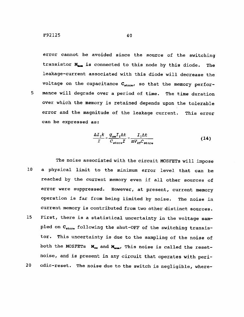
F92125 40
error cannot be avoided since the source of the switching
transistor M._ is connected to this node by this diode. The
leakage-current associated with this diode will decrease the
voltage on the capacitance C.to_ , so that the memory perfor-
5 mance will degrade over a period of time. The time duration
over which the memory is retained depends upon the tolerable
error and the magnitude of the leakage current. This error
can be expressed as:
AI1k-g_IiAt- IiAt (14)I Cstore/ mVkTCstor e
The noise associated with the circuit MOSFETs will impose
i0 a physical limit to the minimum error level that can be
reached by the current memory even if all other sources of
error were suppressed. However, at present, current memory
operation is far from being limited by noise. The noise in
current memory is contributed from two other distinct sources.
15 First, there is a statistical uncertainty in the voltage sam-
pled on C.to_ following the shut-OFF of the switching transis-
tor. This uncertainty is due to the sampling of the noise of
both the MOSFETs M n and M.., This noise is called the reset-
noise, and is present in any circuit that operates with peri-
20 odic-reset. The noise due to the switch is negligible, where-


F92125 41
as the noise in memorizing MOSFET determines the reset noise
and the uncertainty in the voltage sampled is given by:
_. _ kT (15)C,tore
Further, during the readout of the current memory, the channel
noise is also present and causes another error in the
5 memorized current. At the same time, because of the periodic
reset of the circuit, it reduces the low-frequency i/f noise
of the current memory.
When the CMOS counters will not fit under the limited
pixel areas with its cell unit, a row of N photoelectron
i0 counters may be produced on the extended silicon semiconductor
area together with the digital memory, one digital counter for
each column of the NxN pixel array, each to be time shared by
all N pixels in the column. As these N digital counters com-
plete sampling a row of N pixels over a timed integration
15 period, the contents of the counters are transferred serially
or in parallel to a corresponding row of N registers in the
digital memory. The necessary address decoding and timing
circuits are also produced on that extended silicon semicon-
ductor area. In an extreme case of very high definition, it
20 may be necessary to place even the unit cell amplifier for
each of the pixels in the extended part of the silicon


F92125 42
semiconductor layer next to the digital converters. In that
case, only N time shared unit cells are provided, one for each
of N photoelectron counters for each of N columns of pixels.
Improved Readout Circuitry
5 Although the readout circuits in FIGs. 3a and 3b through
FIGs. 5a and 5c may be found in the literature in other
contexts, i.e., in other architectures, the following unique
readout circuits will provide better performance for low light
level imaging with lower voltage and power requirements in
10 either monolithic or hybrid architectures. MCP detector
arrays which operate at a high voltage (2000 volts), large
effective pixels (40 _m resolution), low intrinsic quantum
efficiency at Lyman-a (1216A, 8%), high sensitivity to water
vapor and the need to be periodically "scrubbed" for
15 stability. CCD detector arrays offer large formats, low noise
readout and do not require such high voltages, but have an
equally unappealing collection of limitations. These include
the need for backside illumination or frontside application of
a down converting phosphor.
20 Backside illumination calls for thinning a large area
device and then treating the mechanically fragile surface to
ensure electrical stability and high UV QE. The use of a
frontside phosphor results in more limited QE and cutoff at


F92125 43
about 500 _. The high vapor pressure of the phosphor, and its
tendency to crystallize leads to long term reliability
concerns.
Other issues important for CCDs are their fundamental
5 sensitivity to radiation (e.g., proton) damage that signifi-
cantly reduces charge transfer efficiency and hence signal
fidelity, and residual read noise (3-5 e- rms) that precludes
photon counting. It should also be noted that while sub-
electron read noise has been demonstrated for CCDs using
i0 multiple non-destructive sampling, the transport of single
electrons (or even a few electrons) across macroscopic
distances has not yet been demonstrated. (CTE is typically
quoted for more than 1000 electrons in a charge packet, and
with enough illuminated pixels to ensure that single electron
15 traps are filled.)
While both CCD and MCP approaches find supporters and
continue to be improved, one would like to ideally combine the
photocounting ability of the MCP detector array with the com-
parative ease of solid-state monolithic detectors whenever the
20 photoelectron conversion material can also be used for the
readout circuits, as in the case of CMOS circuits for PIN
photodetector diodes. This is so it would be possible to have
a detector array that could count photoelectrons as they are
generated within the pixel so that the readout could be digi-


F92125 44
tal and hence noise free. The present invention is thus in-
tended to provide an advanced solid-state monolithic photon-
counting imaging device when possible that represents a next-
generation sensor beyond the microchannel plate (MCP) device.
5 The monolithic device is a focal-plane array that
consists of a fully-depleted PIN silicon detector array with
100% fill-factor and high QE, made possible by a
photoelectron-counting silicon CMOS readout with a multi-
plexer. The purpose of this device is to count individual
i0 photoelectrons on the focal plane at a much higher rate than
is presently possible with the MCP/MAMA or strip and wedge
readout system (-i000 counts/pixel/sec) with higher spatial
resolution and low voltage operation. The device will have a
25 micron spatial resolution, and quantum efficiency and dark
15 current similar to that of backside illuminated CCDs (QE a 20%
at 100-400 nm, dark current of 40 count_/pixel/sec at -50°C).
The array format may be readily provided with a i024xi024
pixel array based on proven infrared hybrid focal-plane array
technology. Its main advantage is that the device will not
20 require high voltages typical of MCPs, thus simplifying
associated electronics and packaging. The size of the pixel
will scale with commercial microelectronics minimum feature
sizes and thus will have even higher resolution in succeeding
generations. Since the readout multiplexer uses the common


F92125 45
CMOS fabrication process widely used in space applications,
the radiation hardening of the multiplexer to levels that are
orders of magnitude greater than that of the CCD is also
readily achievable.
5 The open-face nature of the PIN focal-plane detector
array permits inclusion of UV QE enhancement technology under
development for backside illuminated CCDs (e.g., various
pinning technologies, down-converting phosphors, molecular
beam epitaxy of thin silicon films, etc.), and will hence
i0 always have a QE equal to that of backside illuminated CCDS.
Thus, this invention sets the stage for a new class of
UV/visible detectors that will compete favorably against the
MCP technology as well as small format (si0242) CCDS, especi-
ally under low light level conditions. The detectors will be
15 applicable to a wide range of future UV/visible image detec-
tors for large and small missions.
The critical component of the improved device is the
photoelectron-counting readout unit cell design. PIN detector
arrays are already commercially available from Hughes Techno-
20 logy Center (HTC) as noted hereinbefore, albeit with a analog
multiplexer that has much higher noise (>50 electrons rms),
which lends itself to a hybrid architecture, but which is more
advantageously used in a monolithic solid-state architecture.
Thus, in either architecture the primary novelty of the


F92125 46
present invention is the photoelectron-counting circuitry.
The proposed unit cell contains a ultra-low power (<i _W),
very high gain amplifier (A>200,000) with an embedded i/f
noise reduction scheme that extensive circuit analysis and
5 simulation has already shown to exhibit sub-electron input-
referred noise levels. This unit cell gives high confidence
that a photoelectron counting circuit can be achieved in
minimal pixel area.
Referring to FIGs. 1 and ib, which show the photons are
i0 incident on the front surface where they are converted to
electron-hole pairs through the photo-absorption process. The
electrons diffuse through the thin, neutral p-region of the
PIN photodetector diodes and enter the electric field region
(I-layer). They drift through the depleted I-layer and then
15 are collected in the neutral n-region. The photoelectron
charges the capacitance of the buffer amplifier that includes
the detector capacitance as well as the CMOS connection capa-
citance, input transistor gate capacitance, and parasitic
circuit capacitances resulting in change in input voltage to
20 a digital counter. A digital readout multiplexer out of the
counter typically consists of a source-follower amplifier and
selection transistors for gating the readout.
Infrared focal-plane arrays of the prior art use analog
CMOS readout multiplexers. Typical read noise levels for the

F92125 47
most advanced multiplexers (e.g., low background) are in the
range of 30-50 electrons rms, though with multiple nondestruc-
tive readout techniques, noise levels as low as i0 electrons
rms have been reported. The major source of noise is present-
5 ly believed to be random noise introduced on the focal plane
from clocking signals. The intrinsic unit cell noise is domi-
nated by MOSFET i/f noise for low light level signal detection
involving long integration times and is of the order of I0
electrons rms. To date, there has been no report of any ana-
l0 log readout system that attempts to quantify photoelectrons
within the unit cell. The overall design of a pixel unit cell
capable of detecting a single photoelectron is as follows:
i. The required gain of the cell buffer amplifier is
approximately 200,000. The cell size, using 0.8 _m
15 design rules, is estimated to be 25 _m x 25 _m. It
is estimated the unit cell will be capable of
counting up to i000 photoelectrons per second and
dissipate less than 1 _W of power.
2. Assemble the unit cells in a CMOS circuitry plane
20 with an on-chip scanner and accumulator circuits
for reading out the unit cells which include a
digital counter for photon flux integration. The
single bit output of each cell buffer amplifier is


F92125 48
accumulated in an array of dedicated counters
located adjacent to, the detector array. This
counter array is then accessed to readout the
photon flux detected. The output of the counter
5 array is the digital representation of the photon
flux incident on each pixel.
The basis for the unit cell high gain buffer amplifier with an
embedded i/f noise rejection scheme for simultaneously
achieving low noise, high gain, low power and small real
i0 estate amplifier circuits is a novel self-cascoding FET
(SCFET) shown in FIG. 6a. The SCFET is compatible with low
power operations, requires virtually no extra real estate, and
features high output impedance.
The amplifier should be configured to operate in sample-
15 and-subtract mode, so that the i/f noise sample collected
during the reset phase of operation is subtracted during the
high gain phase, thereby directly reducing i/f noise.
The SCFET of FIG. 6a is a common-gate composite
transistor consisting of a cascoding transistor Mc connected
20 in series with the controlling transistor M,. The dimensions
of the two transistors are properly chosen so that the
cascoding transistor M c acts as a screen gate shielding the
main transistor MI from all the variations at the output node,
thereby increasing the output resistance. It has been


F92125 49
demonstrated that a twenty-fold increment in the output
resistance can be achieved with ease.
A buffer amplifier and a comparator fed by the SCFET is
implemented using a cascode differential amplifier as shown in
5 FIG. 6b. The reason for choosing the cascode differential
topology is to increase gain due to cascoding, increase power
supply rejection ratio due to a small common mode gain, in-
crease output impedance due to cascoding, and provide band-
width control by changing the bias current. For the SCFET
10 differential amplifier to be used for electron counting
applications, it is required to possess self-biasing
capability. Auto biasing by dynamic analog techniques will
fail to work because of the high gain of the amplifier in
question. The high gain of the circuit amplifies the effect
15 of any residual switch-feedthrough causing the amplifier to be
driven into saturation.
The novel switch-feedthrough canceling self-biased
differential cascode amplifier shown in FIG. 6b is preferred.
In this circuit, the composite transistors Mil and M_ are the
20 input transistors, ML, and M_ are the load transistors, and M b
is the bias transistor. Because of the increased output
resistance of the SCFET, the differential amplifier possesses
a large gain for a single stage (-500). This value can be


F92125 50
further increased, if necessary, through controlled positive
feedback circuitry.
The switch-feedthrough cancellation scheme takes
advantage of the low common mode gain and large common mode
5 range available in differential topology. By allowing the
switch feedthrough (as a result of the shutting off of the
switch _) to occur in common mode, its effect can be
completely suppressed.
The self-biasing action also results in i/f noise
i0 reduction due to the sample-and-subtract operation inherent in
it. The noise analysis for such periodically resetting
amplifiers have been carried out by the coinventor in his
Ph.D. dissertation cited above and closed form expressions for
noise have been derived. These closed form expressions have
15 emerged as extremely helpful tools in predicting noise
performance of the i/f noise reducing amplifier for a given
bias current (Ib) and sample period (T.). Using the results
derived in the dissertation, the input-referred noise can be
written as:


F92125 51
where g_ and g_ are the transconductances of the input and
the load FETS, fc is the cut-off frequency of the amplifier,
L I and L 2 are the channel lengths, tr is the response time,
is the mobility, C= is the oxide capacitance per unit area,
5 and K s and Kf. are the flicker noise coefficients. This
design equation allows the choice of an optimum channel length
and width for maximizing the signal-to-noise ratio.
Since the proposed circuit operates by counting single
photoelectrons, the dynamic range is determined by the
i0 shortest and the longest possible wait times (i.e. the time
interval between the arrival of consecutive photons) of the
circuit. The maximum wait-time is determined by the tolerable
i/f noise. From Equation (16), it can be seen that the I/f
noise depends on the ratio between the sample-period (T.) and
15 the response-time (£r)- Since, the response time cannot be
increased beyond 0.5 msec without paying severe penalty in
terms of load capacitance size, T./2t r ratio can be as high as


F92125 52
i0,000 for ultra-low level signal-detection. From Equation
(16), the increase in the rms i/f noise voltage is found to be
only one-and-half times, which means that even for extremely
long wait times, i/f noise will not be critically large. The
5 shortest possible wait time, on the other hand, is determined
by the tolerable white noise. It has been demonstrated that
sub-electron input-referred noise is achieved over a large
range of response time values. Further, there exists a trade
off between the minimum response time for which single
i0 electron detection is possible and the power budget. A
typical number for the minimum response time is about 50 _sec,
indicating that the dynamic range is more than 50,000 and the
maximum count rate is greater than i000 per pixel per sec.,
which is orders of magnitude higher than what is achievable
15 with MCPS.
FIG. 7 illustrates the manner in which the buffer
amplifier described with reference to FIGs. 6a and 6b may be
employed to implement the readout circuit of FIG. 3a using two
buffer amplifiers in cascade for sensitivity given by
AVo- AIA2_q _lOmV (17)Cd


F92125 53
for Cd=4OfF
At=A2=50
_rmtl and #_t2 are internal resets required for biasing the gain
stages. For photon counting, neither accurate gain nor
stability is required. Gain of 50-100 per stage is enough.
FIG. 8 illustrates a CMOS circuit diagram for cascaded
5 self-biased amplifiers with cascode input for reduction of
Miller capacitance. Reset noise is dominated by C, and C2, not
by small parasitic input capacitance. Feedthrough on capaci-
tors CI and C 2 limit utility for biasing the high-gain stage,
with a total gain of approximately 5,000 to i0,000. However,
i0 this circuit design is not unity gain stable and therefore
cannot be used for the circuit of FIG. 3a.
FIG. 9 illustrates a power saving scheme for a buffer
amplifier connected directly to a PIN pixel diode 16. However
such a readout circuit creates some concern for parasitic
15 capacitance coupling during transition from high to low bias
current and speed of switching bias currents that must be
attended to in the CMOS layout.
FIG. i0 illustrates a self-biased SCFET buffer amplifier
with cascode input for reduction of Miller capacitance that
20 can be used for the circuit of FIG. 3b.


F92125 54
FIG. II illustrates schematically a hybrid architecture
for the readout system of FIG. i with an address decoder 20
for gating a unit cell buffer amplifier (CTIA or SCFET) to a
row 21 of digital counters which can be serially read out if
5 desired and an address decoder 22 for gating the time shared
row of counters into discrete rows of digital registers in a
buffer memory 23. This arrangement of a CMOS buffer amplifier
provided in an integrated silicon chip, one buffer amplifier
for each pixel in the silicon chip area underneath the focal-
I0 plane array eliminates the need for ultra-high gain buffer
amplifier at each pixel, and sharing one row 21 of photoelec-
tron digital counters provides semiparallel periodic readout,
while the buffer memory 23 provides an accumulator for
extended storage. A row 24 of shift registers provides
15 ultimate semiparallel periodic readout to a permanent storage
device 25, which may be, for example, a reel of magnetic tape,
all under control of a programmed control unit 26.
In the event a complete unit cell comprising a buffer
amplifier and a 10-bit digital counter can be integrated in
20 CMOS circuitry in the silicon area under each reticulated
pixel area, the row of counters 21 may be omitted. The
decoders 20 and 22 normally coordinate control of the buffer
amplifiers of the focal-plane array. Time shared counters 21
and the buffer memory 23 plus the readout shift register 24


F92125 55
under the control of the unit 26 would then need to coordinate
the focal-plane array and counters together and the transfer
of the contents of the digital counters to the buffer memory
and from there to the output shift register 24 for extended
5 memory also under control of the unit 26.
For a monolithic architecture comparable to that of the
hybrid architecture in FXG. i0, there are virtually no
constraints in the CMOS layout adopted. It would be possible
to provide the SCMOS buffer amplifier and CMOS 10-bit counter
i0 in a single readout cell with the PIN photodetector diode
connected to the input terminal of the amplifier. Each pixel
may then be read out in sequence or in parallel row by row
into the buffer memory. However, it would also be possible to
time share a row of digital counters as in the hybrid
15 structure. The advantage of the monolithic architecture is to
be found not only in improved performance, but also in the
ease of fabrication.
Although particular embodiments of the invention have
been described and illustrated herein, it is recognized that
20 modifications may readily occur to those skilled in the art.
Consequently it is intended that the claims be interpreted to
cover such modifications and equivalents thereof.


F92125
SOLID-STATE IMAGE SENSOR WITH FOCAL-PLANE
DIGITAL PHOTON-COUNTING PIXEL ARRAY
ABSTRACT OF THE DISCLOSURE
A photosensitive layer such as a-Si for a UV/visible
5 wavelength band is provided for low light level imaging with
at least a separate CMOS amplifier directly connected to each
PIN photodetector diode to provide a focal-plane array of NxN
pixels, and preferably a separate photon-counting CMOS circuit
directly connected to each CMOS amplifier, although one row of
10 counters may be time shared for reading out the photon flux
rate of each diode in the array, together with a buffer memory
for storing all rows of the NxN image frame before transfer to
suitable storage. All CMOS circuitry is preferably fabricated
in the same silicon layer as the PIN photodetector diode for
15 a monolithic structure, but when the wavelength band of inter-
est requires photosensitive material different from silicon,
the focal-plane array may be fabricated separately on a dif-
ferent semiconductor layer bump-bonded or otherwise bonded for
a virtually monolithic structure with one free terminal of
20 each diode directly connected to the input terminal of its
CMOS amplifier and digital counter for integration of the
photon flux rate at each photodetector of the array.


',,,,//\/

NASA Case No. NPO-18518-I-CU
Page I of 8SOLID-STATE IMAGE SENSOR WITH
FOCAL-PLANE DIGITAL PHOTON-COUNTING PIXEL ARRAY
Inventor: Eric R. Fossum, et al.
Contact: John H. Kusmiss
Telephone No. 818-354-7770

-___--_1_--_! _,h O r,,.J"_--_- :r Cd
/o/_-.I_ c<__/_-IU.Jo.__ol,,,,,,,.,,..
4,ist
,,, "__,I'_ +_,I,,

NASA Case No. NPO-18518-I-CU
Page 2 of 8SOLID-STATE IMAGE SENSOR WITH
FOCAL-PLANE DIGITAL PHOTON-COUNTING
PIXEL ARRAY
Inventor: Eric R. Fossum, et al.
Contact: John H. Kusmlss
Telephone No. 818-354-7770

" VpVdel
IICf

"'_-"/ 909_
:x ' _/o,-/ 20
NASA Case No. NPO-18518-1-CU
Page 3 of 8SOLID-STATE IMAGE SENSOR WITH
FOCAL-PLANE DIGITAL PHOTON-
COUNTING PIXEL ARRAY
Inventor: Eric R. Fossum, et al.
Contact: John H. Kusmiss
Telephone No. 818-354-7770


NASA Case No. NPO-18518-1-CU
Page 4 of 8SOLID-STATE IMAGE SENSOR WITH FOCAL-PLANE DIGITAL PHOTON-COUNTING PIXEL
ARRAY
Inventor: Eric R. Fossum, et al.
Contact: John H. Kusmlss
Telephone No. 818-354-7770


c _LIII(;III F----l--,
--IIL RI:.SliT
MIllelll
F.quiv. Circuit of Ci.iI'llc_lc._deteclol"
I{ _,I I_i ' __ " A v __ v !
T , Ib v,_
)'"

_.o.<-I ,_"o¢ ,?NASA Case No. NPO-IB518-I-CU
Pa_e 5 _ 8SOLID-STATE IMAGE SENSOR WITH
FOCAL-PLANE DIGITAL PHOTON-
COUNTING PIXEL ARRAY
Inventor: Eric R. Fossum, et al.
Contact: John H. Kusmiss
Telephone No. 818-354-7770

v<j,I,_ -T-v"", ,_.1 ]/lli
-- - / Vss
(li rsl
___ -- V o
Col,l,,n bus

_£_/.. 0990
" ; 6 _7/,_I
NASA Case No. NPO-18518-I-CU
Page 6 of 8SOLID-STATE IMAGE SENSOR WITH
FOCAL-PLANE DIGITAL PHOTON-
COUNTING PIXEL ARRAY
Inventor: Eric R. Fossum, et al.
Contact: John H. Kusmlss
Telephone No. 818-354-7770

Vdd
1 1V
'" q£ _F-r2 v
¢
v _8_i ct I_ --_ o.tV
casc_ [_. El& £
°" -I I--1_, -HE IE, I 1Vss
VddVdd
-'l":s' v._[-
l__inCl, _ R Ih,gh 'll L (,,)

NASA Case No. NPO-18518-1-CU
Page 7 of 8SOLID-STATE IMAGE SENSOR WITH FOCAL-
PLANE DIGITAL PHOTON-COUNTING
PIXEL ARRAY
Inventor: Eric R. Fossum, et al.
Contact: John H. Kusmiss
Telephone No. 818-354-7770


NASA Case No. NPO-18518-I-CU
Page 8 of 8SOLID-STATE IMAGE SENSOR WITHFOCAL-PLANE DIGITAL PHOTON-
COUNTING PIXEL ARRAY
Inventor: Eric R. Fossum, et al.
Contact: John Kusmlss
Telephone No. 818-354-7770