nanotechnology || what is nanotechnology?
TRANSCRIPT

“04-ch01-001-014-9780080964478” — 2011/6/30 — 1:54 — page 1 — #1
CHAPTER
What is Nanotechnology? 1C H A P T E R C O N T E N T S
1.1 Definitions and Concepts .. . . . . . . . . . . . . . . . . . . . . . . . . . . . . . . . . . . . . . . . . . . . . . . . . . . . . . . . . . . . . 21.1.1 Working Definitions . . . . . . . . . . . . . . . . . . . . . . . . . . . . . . . . . . . . . . . . . . . . . . . . . . . . 21.1.2 Towards a Concept System for Nanotechnology . . . . . . . . . . . . . . . . . . . . . . . 3
1.2 An Ostensive Definition of Nanotechnology ... . . . . . . . . . . . . . . . . . . . . . . . . . . . . . . . . . . . . . . . 51.3 A Brief History of Nanotechnology ... . . . . . . . . . . . . . . . . . . . . . . . . . . . . . . . . . . . . . . . . . . . . . . . . . 5
1.3.1 Ultraprecision Engineering . . . . . . . . . . . . . . . . . . . . . . . . . . . . . . . . . . . . . . . . . . . . . 71.3.2 Semiconductor Processing qua Microtechnology . . . . . . . . . . . . . . . . . . . . . . 71.3.3 Nanoparticles . . . . . . . . . . . . . . . . . . . . . . . . . . . . . . . . . . . . . . . . . . . . . . . . . . . . . . . . . . 9
1.4 Biology as Paradigm .... . . . . . . . . . . . . . . . . . . . . . . . . . . . . . . . . . . . . . . . . . . . . . . . . . . . . . . . . . . . . . . . 101.5 Why Nanotechnology? ... . . . . . . . . . . . . . . . . . . . . . . . . . . . . . . . . . . . . . . . . . . . . . . . . . . . . . . . . . . . . . . 11
1.5.1 Novel Combinations of Properties. . . . . . . . . . . . . . . . . . . . . . . . . . . . . . . . . . . . . . 111.5.2 Device Miniaturization: Functional Enhancement . . . . . . . . . . . . . . . . . . . . . 131.5.3 A Universal Fabrication Technology . . . . . . . . . . . . . . . . . . . . . . . . . . . . . . . . . . . . 14
1.6 Summary... . . . . . . . . . . . . . . . . . . . . . . . . . . . . . . . . . . . . . . . . . . . . . . . . . . . . . . . . . . . . . . . . . . . . . . . . . . . . . 141.7 Further Reading ... . . . . . . . . . . . . . . . . . . . . . . . . . . . . . . . . . . . . . . . . . . . . . . . . . . . . . . . . . . . . . . . . . . . . . 14
Nanotechnology is above all a mindset, a way of thinking about the world that isrooted in atomically precise perception. As such, it represents the apotheosis ofman’s ceaseless urge to understand the world and use that understanding for prac-tical purposes. Well synonymized as “atomically precise technology”, it encapsulatesthe vision of building “our earthly estate” atom-by-atom, controlling architecture,composition and hence physical properties with atomic resolution. “Hard” nanotech-nologists promote a future world in which every artifact (and even food) can beconstructed atom-by-atom from a feedstock such as acetylene, requiring in addi-tion only energy and instructions. A more pragmatic view accepts that there aremany intermediate stages in which partially atomically precise construction canimprove existing artifacts and create new ones. Similarly, the resolute aim of “hard”nanotechnologists is to create productive nanosystems (PN) working with atomicprecision—the nanoscale assemblers that would execute the instructions and buildeverything we need from the bottom upwards, whereas a more pragmatic viewaccepts that while in principle everything can be reproduced and many things imi-tated via atom-by-atom assembly, in many cases the improvement in properties orperformance would be negligible and a hybrid approach will best serve the needs of
Nanotechnology: An Introduction. DOI: 10.1016/B978-0-08-096447-8.00001-6Copyright c© 2011. Published by Elsevier Inc. All rights reserved.
1

“04-ch01-001-014-9780080964478” — 2011/6/30 — 1:54 — page 2 — #2
2 CHAPTER 1 What is Nanotechnology?
humanity. This is particularly likely to be the case for large artifacts (such as humandwellings or airplanes) and for relatively complex products such as food, which canbe quite easily grown naturally.
In this chapter we shall first look at the basic definitions for nanotechnology,and sketch a concept system (“ontology”) for the field. It is also possible to definenanotechnology ostensively, according to what is already generally considered to benanotechnology, and extended by what is envisaged in the future. A further way ofdefining it is through its history. We also briefly look at the relation of nanotechnologyto biology, which has been a powerful paradigm for convincing engineers that nano-technology is possible—nanobiotechnology and bionanotechnology form the topicsof subsequent chapters (4 and 11 respectively). General motivations for nanotechnol-ogy are considered—“Why nanotechnology?” Attention is drawn to the appended listof neologisms associated with nanotechnology (Appendix, p. 247).
1.1 DEFINITIONS AND CONCEPTS1.1.1 Working DefinitionsThe simplest definition of nanotechnology is “technology at the nanoscale”. The vari-ous definitions currently circulating can be reasonably accurately thus paraphrased.Obviously, this definition is not intelligible in the absence of a further definition,namely that of the nanoscale. Furthermore, definitions of components of nanotechnol-ogy, such as “nanofiber”, also refer to the nanoscale; indeed every word starting with“nano”, which we can generically write as “nanoX”, can be defined as “nanoscaleX”. Therefore, unless we define “nanoscale”, we cannot therefore properly definenanotechnology. A rational attempt to do so is made in Chapter 2. Here we notethat provisionally, the nanoscale is considered to cover the range from 1 to 100 nm.Essentially this is a consensus without a strong rational foundation.
A slightly longer but still succinct definition of nanotechnology is simply “engi-neering with atomic precision”, or “atomically precise technology” (APT). However,this definition does not explicitly include the aspects of “fundamentally new proper-ties” or “novel” and “unique” that nanotechnologists usually insist upon, wishing toexclude existing artifacts that happen to be small. These aspects are encapsulated bythe US National Nanotechnology Initiative’s declaration that “the essence of nano-technology is the ability to work at the molecular level, atom-by-atom, to create largestructures with fundamentally new molecular organization . . . nanotechnology is con-cerned with materials and systems whose structures and components exhibit noveland significantly improved physical, chemical, and biological properties, phenomena,and processes due to their nanoscale size” [123].
The US Foresight Institute gives “nanotechnology is a group of emerging tech-nologies in which the structure of matter is controlled at the nanometer scaleto produce novel materials and devices that have useful and unique properties”.

“04-ch01-001-014-9780080964478” — 2011/6/30 — 1:54 — page 3 — #3
1.1 Definitions and Concepts 3
Function is stressed in: “the design, synthesis, characterization and application ofmaterials, devices and systems that have a functional organization in at least onedimension on the nanometer scale”. This is emphasized even more strongly in “nano-technology pertains to the processing of materials in which structure of a dimensionof less than 100 nm is essential to obtain the required functional performance” [36].
In all such definitions, there is the implicit meaning that, as for any technology,the end result must be of practical use. A dictionary definition of nanotechnology is“the design, characterization, production and application of materials, devices andsystems by controlling shape and size in the nanoscale” [1]. An alternative definitionfrom the same dictionary is “the deliberate and controlled manipulation, precisionplacement, measurement, modeling and production of matter in the nanoscale inorder to create materials, devices, and systems with fundamentally new propertiesand functions” [1]. The emphasis on control is particularly important: it is this thatdistinguishes nanotechnology from chemistry, with which it is often compared. Inthe latter, motion is essentially uncontrolled and random, within the constraint that ittakes place on the potential energy surface of the atoms and molecules under con-sideration. In order to achieve the desired control, a special, nonrandom eutacticenvironment needs to be available. How eutactic environments can be practicallyachieved is still being vigorously discussed. Finally, a definition of nanotechnologyattempting to be comprehensive is “the application of scientific knowledge to meas-ure, create, pattern, manipulate, utilize or incorporate materials and components inthe nanoscale”. This underlines the idea of nanotechnology as the consummation ofStage 4 in the sequence of technological revolutions that marks the development ofhuman civilization (Table 12.1 in Chapter 12).
It is sometimes debated whether one should refer to “nanotechnology” or “nano-technologies”. The argument in favor of the latter is that nanotechnology encom-passes many distinctly different kinds of technology. But there seems to be no reasonnot to use “nanotechnology” in a collective sense, since the different kinds are never-theless all united by striving for control at the atomic scale. Both terms are, in fact,legitimate. When one wishes to emphasize diverse applications, the plural form isappropriate. The singular term refers above all to the mindset or attitude associatedwith the technology.
1.1.2 Towards a Concept System for NanotechnologyObjects are perceived or conceived. The properties of an object (which may be com-mon to a set of objects) are abstracted into characteristics. Essential characteristics(feature specifications) typically falling into different categories (e.g., shape, color)are combined as a set to form a concept; this is how objects are abstracted into con-cepts, and the set of essential characteristics that come together as a unit to form aconcept is called the intension. The set of objects abstracted into a concept is called theextension. Delimiting characteristics distinguish one concept from another. Conceptsare described in definitions and represented by designations. The set of designations
“04-ch01-001-014-9780080964478” — 2011/6/30 — 1:54 — page 4 — #4
4 CHAPTER 1 What is Nanotechnology?
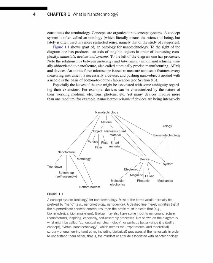
constitutes the terminology. Concepts are organized into concept systems. A conceptsystem is often called an ontology (which literally means the science of being, butlately is often used in a more restricted sense, namely that of the study of categories).
Figure 1.1 shows (part of) an ontology for nanotechnology. To the right of thediagram one has products—an axis of tangible objects in order of increasing com-plexity: materials, devices and systems. To the left of the diagram one has processes.Note the relationships between metrology and fabrication (nanomanufacturing, usu-ally abbreviated to nanofacture, also called atomically precise manufacturing, APM)and devices. An atomic force microscope is used to measure nanoscale features; everymeasuring instrument is necessarily a device; and pushing nano-objects around witha needle is the basis of bottom-to-bottom fabrication (see Section 8.3).
Especially the leaves of the tree might be associated with some ambiguity regard-ing their extensions. For example, devices can be characterized by the nature oftheir working medium: electrons, photons, etc. Yet many devices involve morethan one medium: for example, nanoelectromechanical devices are being intensively
Nanotechnology
Material
Object
Smartmaterial
Plate
Fiber
Particle
Metrology
Nanofacture
Top–down
Bottom–up(self-assembly)
Bottom-bottom
Molecularelectronics
Photonic
FluidicMagnetic
Electronic
Mechanical
System
Bionanotechnology
Biology
Device
Nanostructuredmaterial
FIGURE 1.1
A concept system (ontology) for nanotechnology. Most of the terms would normally beprefixed by “nano” (e.g., nanometrology, nanodevice). A dashed line merely signifies that ifthe superordinate concept contributes, then the prefix must indicate that (e.g.,bionanodevice, bionanosystem). Biology may also have some input to nanomanufacture(nanofacture), inspiring, especially, self-assembly processes. Not shown on the diagram iswhat might be called “conceptual nanotechnology”, or perhaps better (since it is itself aconcept), “virtual nanotechnology”, which means the (experimental and theoretical)scrutiny of engineering (and other, including biological) processes at the nanoscale in orderto understand them better; that is, the mindset or attitude associated with nanotechnology.

“04-ch01-001-014-9780080964478” — 2011/6/30 — 1:54 — page 5 — #5
1.3 A Brief History of Nanotechnology 5
Table 1.1 Some nano concepts and their intensions and extensions
Intension Concept Extension
One or more external dimensionsin the nanoscale
Nano-object Graphene, fullerene
One or more geometrical featuresin the nanoscale
Nanomaterial A nanocomposite
Automaton with informationstorage and/or processingembodiments in the nanoscale
Nanodevice Single electron transistor
researched as a way of achieving electronic switching; optoelectronic control is apopular way of achieving photonic switching; and photochemistry in miniaturizedreactors involves both nanophotonics and nanofluidics.
Table 1.1 describes a few of the concepts and their intensions and extensions.At the time of writing, the terminology of nanotechnology is still being intensivelydebated within national standards organizations as well supranational bodies suchas the Comite Europeen de Normalisation (CEN) and the International StandardsOrganization (ISO), hence no attempt has been made to be comprehensive here.
1.2 AN OSTENSIVE DEFINITION OF NANOTECHNOLOGYAn ostensive definition of current nanotechnology can be constructed from the mostpopular topics (Table 1.2), essentially extensions in the sense of Section 1.1.2.
A number of inferences can be drawn from this table, including the preeminenceof carbon as a nanomaterial, the nanoparticle as a nano-object, and energy, compos-ites (materials) and sensors as applications. Interestingly, “water” features highly onthe list. The reasons for this will be apparent from reading Section 3.8.
A very simple (albeit privative) ostensive definition of nanotechnology is “If youcan see it (including with the aid of an optical microscope), it’s not nano”, referringto the fact that any object below 100 nm in size is below the Abbe limit for opticalresolution using any visible wavelength (equation 5.2). A nanoplate, however, wouldonly be invisible if oriented exactly parallel to the line of sight.
1.3 A BRIEF HISTORY OF NANOTECHNOLOGYReference is often made to a lecture given by Richard Feynman in 1959 at Caltech[56]. Entitled “There’s Plenty of Room at the Bottom”, it expounds his vision ofmachines making the components for smaller machines (a familiar enough oper-ation at the macroscale), themselves capable of making the components for yetsmaller machines, and simply continuing the sequence until the atomic realm is

“04-ch01-001-014-9780080964478” — 2011/6/30 — 1:54 — page 6 — #6
6 CHAPTER 1 What is Nanotechnology?
Table 1.2 Table of the relative importance (ranked bynumbers of occurrences of words in the titles of paperspresented at the Nano2009 Conference in Houston, Texas)of nanotechnology terms and applications
Rank Term Number of occurrences
1 Carbon, CNT 1512 Nanoparticle, nanocrystal 1383 Energy 964 (Nano)material 925 Nanotube 826 (Nano)composite 797 (Bio)sensor 558 Water 459 Device 33
10 Nanowire 3311 Assembly 3112 Silicon 3013 Zinc (oxide) 2614 Titanium (oxide) 2515 Quantum 2416 Silica 2117 Phage 2018 Bio 1919 Photovoltaic 1520 Nanorod 821 Graphene 722 Nanopore 723 Silver 7
reached. Offering a prize of $1000 for the first person to build a working electricmotor with an overall size not exceeding 1/64th of an inch, Feynman was dismayedwhen not long afterwards a student, William McLellan, presented him with a labori-ously hand-assembled (i.e., using the technique of the watchmaker) electric motor ofconventional design that nevertheless met the specified criteria.
A similar idea was proposed at around the same time by Marvin Minsky: “Clearlyit is possible to have complex machines the size of a flea; probably one can havethem the size of bacterial cells . . . consider contemporary efforts towards construct-ing small fast computers. The main line of attack is concentrated on “printing”or evaporation through masks. This is surely attractive; in one operation one canprint thousands of elements. But an alternative, equally attractive, has been ignored.Imagine small machines fabricating small elements at kilocycle rates. (The speed ofsmall mechanical devices is extremely high.) Again, one can hope to make thousandsof elements per second. But the generality of the mechanical approach is much greatersince there are many structures that do not lend themselves easily to laminar maskconstruction” [118]. One wonders whether Feynman and Minsky had previously

“04-ch01-001-014-9780080964478” — 2011/6/30 — 1:54 — page 7 — #7
1.3 A Brief History of Nanotechnology 7
read Robert A. Heinlein’s short story “Waldo”, which introduces this idea (it waspublished in the August 1942 issue of “Astounding” magazine under the pseudonymAnson MacDonald).
Here we find the germ of the idea of the assembler, a concept later elaborated byEric Drexler. The assembler is a universal nanoscale assembling machine, capable notonly of making nanostructured materials, but also other machines (including copiesof itself). The first assembler would have to be laboriously built atom-by-atom, butonce it was working numbers could evidently grow exponentially, and when a largenumber became available, universal manufacturing capability, hence the nano-era,would have truly arrived (see also Chapter 8).
However, the idea of a minute device intervening at the level of elementary par-ticles was conceived almost a hundred years earlier by James Clerk Maxwell whenhe conceived his “demon” for selectively allowing molecules to pass through a door,thereby entangling physics with information. Perhaps Maxwell should be consid-ered as the real father of nanotechnology. The demon was described in Maxwell’sTheory of Heat first published in 1871, but had already been mentioned in earliercorrespondence of his.
1.3.1 Ultraprecision EngineeringIt could well be said that the history of technological advance is the history of everfiner tolerances in machining metals and other materials. A classic example is thesteam engine: James Watt’s high-pressure machine that paved the way for the tech-nology to move from a cumbersome and rather inefficient means of pumping waterout of mines to an industrially useful and even self-propelling technology was onlypossible once machining tolerance had improved to enable pistons to slide withincylinders without leaking.
An approach to the nanoscale seemingly quite different from the Heinlein–Feynman–Minsky–Drexler vision of assemblers starts from the microscopic worldof precision engineering, progressively scaling down to ultraprecision engineering(Figure 1.2). The word “nanotechnology” was itself coined by Norio Taniguchi in1974 to describe the lower limit of this process [159]. He referred to “atomic bitmachining”.
1.3.2 Semiconductor Processing qua MicrotechnologyThe trend in ultraprecision engineering is mirrored by relentless miniaturization inthe semiconductor processing industry. The history of the integrated circuit couldperhaps be considered to start in 1904, when Bose patented the galena crystal forreceiving electromagnetic waves, followed by Picard’s 1906 patent for a silicon crys-tal. The thermionic valve and the triode were invented respectively by Fleming (in1904) and de Forest (in 1906), which became the basis of logic gates, reaching zenithwith the ENIAC, which contained about 20,000 valves. The invention of the pointcontact transistor in 1947 at Bell Laboratories essentially rendered the thermionic

“04-ch01-001-014-9780080964478” — 2011/6/30 — 1:54 — page 8 — #8
8 CHAPTER 1 What is Nanotechnology?
200019801960
1nm
Mac
hini
ng a
ccur
acy
1 �m
1mm
Normal machining
Precision machining
Ultraprecision machining
Year
1940
FIGURE 1.2
The evolution of machining accuracy (after Norio Taniguchi).
valve obsolete, but the first commercial use of transistors only occurred in 1953(the Sonotone 1010 hearing aid), the first transistor radio appearing one year later.Meanwhile the idea of an integrated circuit had been proposed by Dummer at theRoyal Signals Research Establishment (RSRE) in 1952, but (presumably) he was notallowed to work on it at what was then a government establishment, and the firstactual example was realized by Kilby in 1958 at Texas Instruments, closely followedby Noyce at Fairchild in the following year. It is interesting to recall that the Apolloflight computer (“Block II”) used for the first moon landing in 1969 was designedin 1964 (the year before Moore’s law was first proposed), used resistor–transistorlogic (RTL) and had a clock speed of 2 MHz. Intel introduced the first microproces-sor, with about 2000 transistors, in 1971, the year in which the pioneering “LE-120AHandy” pocket calculator was launched in Japan. It took another decade before theIBM personal computer appeared (1981); the Apple II had already been launchedin 1977. By 2000, we had the Pentium 4 chip with about 1.2 × 10⁶ transistors fab-ricated with 180 nm process technology. In contrast, today’s dual core Intel Itaniumchip has about 1.7 × 10⁹ transistors (occupying an area of about 50 × 20 mm) witha gate length of 90 nm. A 45 nm transistor can switch 3 × 10¹¹ times per second—this is about 100 GHz. Experimental graphene-based devices achieve more than aTHz. Despite the extraordinarily high precision fabrication called for in such devices,

“04-ch01-001-014-9780080964478” — 2011/6/30 — 1:54 — page 9 — #9
1.3 A Brief History of Nanotechnology 9
modern integrated circuits are reliable enough for spacecraft (for example) to usecommercial off-the-shelf (COTS) devices. The fabrication plants are not cheap—Intel’s 2008 China facility is reputed to have cost $2.5 ×10⁹: a mask alone for a chipmade using 180 nm process technology costs about $100,000, rising to one milliondollars for 45 nm technology. Despite the huge costs of the plant, cost per chip con-tinues to fall relentlessly: for example, a mobile phone chip cost about $20 in 1997,but only $2 in 2007.
The relentless diminution of feature size, and the concomitant increase of thenumber of transistors that can be fabricated in parallel on a single chip, has beenwell documented; structures with features a few tens of nanometers in size capableof being examined in an electron microscope were reported as long ago as 1960;device structures with dimensions less than 100 nm were already being reportedin 1972, with 25 nm achieved in 1979. Incidentally, the lower size limit for prac-tical semiconductor circuits is considered to be 20 nm; smaller sizes, hence highertransistor number densities per unit area, will only be achievable using three-dimensional design or quantum logic (Section 7.3). Thus we see that since thebeginning of nanotechnology—identifying this with the conception of Maxwell’sdemon—nanotechnology has been intimately connected with information scienceand technology.
1.3.3 NanoparticlesIf we define nanotechnology ostensively, we have to concede a very long history:there is evidence that PbS nanocrystals were the goal of a procedure used sinceGreco-Roman times to color hair black [164]. Nanoparticulate gold has a long history,not least in medicine (see Section 4.2). The Flemish glassmaker John Utynam wasgranted a patent in 1449 in England for making stained glass incorporating nanopar-ticulate gold; and the Swiss medical doctor and chemist von Hohenheim (Paracelsus)prepared and administered gold nanoparticles to patients suffering from certainailments in the early 16th century; a modern equivalent is perhaps the magneticnanoparticles proposed for therapeutic purposes. The secret of the extraordinarilyadvanced metallurgical features of Damascus swords made more than 400 years agohas recently been found to be carbon nanotubes embedded in the blades [146].
With such a long history, it is perhaps hardly surprising that at present they rep-resent almost the only part of nanotechnology with commercial significance. Thefabrication of different kinds of nanoparticles by chemical means seems to have beenwell established by the middle of the 19th century (e.g., Thomas Graham’s methodfor making ferric hydroxide nanoparticles [63]). Wolfgang Ostwald lectured exten-sively on the topic in the early 20th century in the USA, and wrote up the lecturesin what became a hugely successful book, Die Welt der vernachlassigten Dimensio-nen. Many universities had departments of colloid science (sometimes considered asphysics, sometimes as chemistry), at least up to the middle of the 20th century, thenslowly the subject seemed to fall out of fashion, until its recent revival as part of

“04-ch01-001-014-9780080964478” — 2011/6/30 — 1:54 — page 10 — #10
10 CHAPTER 1 What is Nanotechnology?
nanotechnology. The field somewhat overlapped that of heterogeneous catalysis, inwhich it was well known, indeed almost obvious, that specific activity (i.e., per unitmass) tended to increase with increasing fineness of division.
1.4 BIOLOGY AS PARADIGMWhen Feynman delivered his famous lecture [56] it was already well known that thesmallest viable unit of life was the cell, which could be less than a micrometer insize. It was surmised that cells contained a great deal of machinery at smaller scales,which has since been abundantly evidenced through the work of molecular biolo-gists. Examples of these machines are molecule carriers (e.g., hemoglobin), enzymes(heterogeneous catalysts), rotary motors (e.g., those powering bacterial flagella),linear motors (e.g., muscle), pumps (e.g., transmembrane ion channels), and multi-enzyme complexes carrying out more complicated functions then simple reactions(e.g., the proteasome for degrading proteins, or the ribosome for translating informa-tion encoded as a nucleic acid sequence into a polypeptide sequence). When Drexlerdeveloped his explicit schema of nanoscale assemblers, allusion to nanoscale biolog-ical machinery was explicitly made as a “living proof-of-principle” demonstratingthe feasibility of artificial devices constructed at a similar scale [43].
At present, probably the most practically useful manifestation of the biologicalnanoparadigm is self-assembly. In simple form, self-assembly is well known in thenonliving world (for example, crystallization). This process does not, however, havethe potential to become a feasible industrial technology for the general-purpose con-struction of nanoscale objects, because size limitation is not intrinsic to it. Only whenhighly regular structures need to be produced (e.g., a nanoporous membrane, or a col-lection of monosized nanoparticles) can the process parameters be set to generate anoutcome of a prespecified size. Nature, however, has devised a more sophisticatedprocess, known to engineers as programmable self-assembly, in which every detailof the final structure can be specified in advance by using components that not onlyinterlock in highly specific ways but are also capable of changing their structure uponbinding to an assembly partner in order to block or facilitate, respectively, previouslypossible or impossible interlocking actions. Inspiration for harnessing programmableself-assembly arose from the work of virologists who noticed that pre-assembledcomponents (head, neck, legs) of bacteriophage viruses would further assemble spon-taneously into a functional virus merely upon mixing and shaking in a test-tube. This“shake and bake ” approach appeared to offer a manufacturing route to nanodevicesobviating: (1) the many difficulties involved in making Drexlerian assemblers, whichwould appear to preclude their realization in the near future; and (2) the great expenseof the ultrahigh precision “top–down” approach, whether via UPMT or semiconduc-tor processing. Even if assemblers are ultimately realized, it might be most advanta-geous to use them to assemble sophisticated “nanoblocks”, designed to self-assembleinto final macroscopic objects (see Section 8.3.2). In other words, self-assembly’s

“04-ch01-001-014-9780080964478” — 2011/6/30 — 1:54 — page 11 — #11
1.5 Why Nanotechnology? 11
greatest potential utility will probably arise as a means to bridge the size gap betweenthe nanoscopic products of assemblers and the macroscopic artifacts of practical usefor humans. Self-assembly is covered in detail in Chapter 8.
1.5 WHY NANOTECHNOLOGY?Nanotechnology is associated with at least three distinct advantages:
1. It offers the possibility of creating materials with novel combinations of proper-ties.
2. Devices in the nanoscale need less material to make them, use less energy andother consumables, their function may be enhanced by reducing the characteristicdimensions, and they may have an extended range of accessibility.
3. It offers a universal fabrication technology, the apotheosis of which is the personalnanofactory.
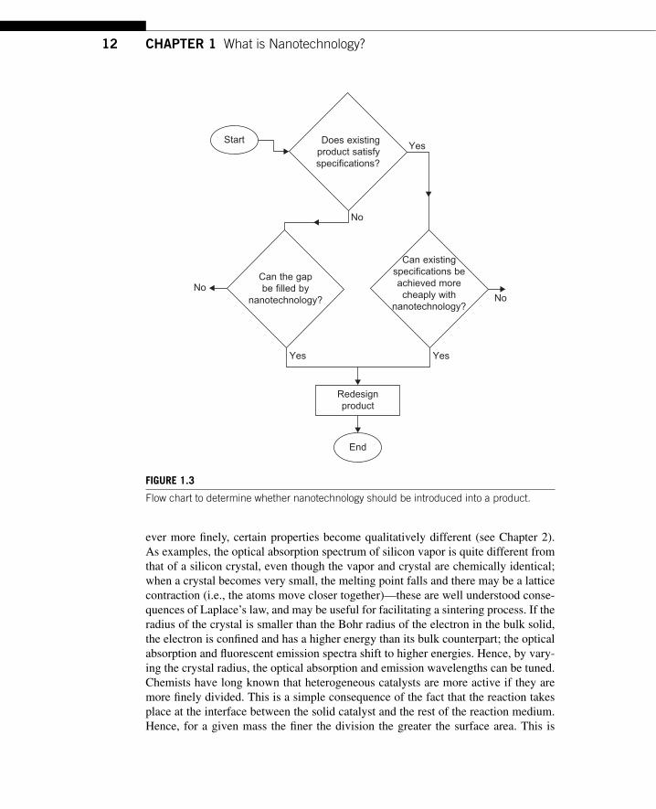
The burgeoning worldwide activity in nanotechnology cannot be explained purelyas a rational attempt to exploit “room at the bottom”, however. Two other impor-tant human motivations are doubtless also playing a role. One is simply “it hasn’tbeen done before”—the motivation of the mountaineer ascending a peak previouslyuntrodden. The other is the perennial desire to “conquer nature”. Opportunities fordoing so at the familiar macroscopic scale have become very limited, partly becauseso much has already been done—in Europe, for example, there are hardly anymarshes left to drain or rivers left to dam, historically two of the most typical arenasfor “conquering nature”—and partly because the deleterious effects of such “con-quest” are now far more widely recognized, and the few remaining undrained marshesand undammed rivers are likely nowadays to be legally protected nature reserves.But the world at the bottom, as Feynman picturesquely called it, is uncontrolled andlargely unexplored. On a more prosaic note, nanotechnology may already offer imme-diate benefit for existing products through substitution or incremental improvement(Figure 1.3). The space industry has a constant and heavily pressing requirementfor making payloads as small and lightweight as possible. Nanotechnology is ideal-ly suited to this end user—provided the nanomaterials, devices and systems can bemade sufficiently reliable (see Chapter 10).
1.5.1 Novel Combinations of PropertiesThere are two ways of creating nanomaterials. One is by adding nano-objects(nanoadditives) to a matrix. For example, organic polymer matrices incorporat-ing carbon nanotubes can be light and very strong, or transparent and electricallyconducting. The other is by fabricating materials de novo, atom-by-atom.
Since it is usually more expensive to create nanosized rather than microsized mat-ter, one needs to justify the expense of downscaling the additives: as matter is divided
“04-ch01-001-014-9780080964478” — 2011/6/30 — 1:54 — page 12 — #12
12 CHAPTER 1 What is Nanotechnology?
Start
NoNo
No
Yes
Can existingspecifications beachieved morecheaply with
nanotechnology?
Can the gapbe filled by
nanotechnology?
Does existingproduct satisfyspecifications?
Yes
Redesignproduct
End
Yes
FIGURE 1.3
Flow chart to determine whether nanotechnology should be introduced into a product.
ever more finely, certain properties become qualitatively different (see Chapter 2).As examples, the optical absorption spectrum of silicon vapor is quite different fromthat of a silicon crystal, even though the vapor and crystal are chemically identical;when a crystal becomes very small, the melting point falls and there may be a latticecontraction (i.e., the atoms move closer together)—these are well understood conse-quences of Laplace’s law, and may be useful for facilitating a sintering process. If theradius of the crystal is smaller than the Bohr radius of the electron in the bulk solid,the electron is confined and has a higher energy than its bulk counterpart; the opticalabsorption and fluorescent emission spectra shift to higher energies. Hence, by vary-ing the crystal radius, the optical absorption and emission wavelengths can be tuned.Chemists have long known that heterogeneous catalysts are more active if they aremore finely divided. This is a simple consequence of the fact that the reaction takesplace at the interface between the solid catalyst and the rest of the reaction medium.Hence, for a given mass the finer the division the greater the surface area. This is

“04-ch01-001-014-9780080964478” — 2011/6/30 — 1:54 — page 13 — #13
1.5 Why Nanotechnology? 13
not in itself a qualitative change, although in an industrial application there may be aqualitative transition from an uneconomic to an economic process.
1.5.2 Device Miniaturization: Functional EnhancementThe response time of a device usually decreases with decreasing size. Informationcarriers have less far to diffuse, or travel ballistically, and the resonant frequency ofoscillators increases (Section 2.7).
Clearly the quantity of material constituting a device scales roughly as the cube ofits linear dimension. Its energy consumption in operation may scale similarly. In themacroscopic world of mechanical engineering, however, if the material costs are dis-regarded, it is typically more expensive to make something very small; for example,a watch is more expensive than a clock, for equivalent timekeeping precision. Onthe other hand when things become very large, as in the case of the clock familiarlyknown as Big Ben for example, costs again start to rise, because special machinerymay be needed to assemble the components, and so on. We shall return to the issueof fabrication in Chapter 8.
Performance (expressed in terms of straightforward input–output relations)may thus be enhanced by reducing the size, although the enhancement does notalways continue ad libitum: for most microelectromechanical systems (MEMS)devices, such as accelerometers, performance is degraded by downscaling below themicroscale (Section 10.8), and the actual size of the devices currently mass-producedfor actuating automotive airbags already represents a compromise between econ-omy of material, neither taking up too much space nor weighing two much, andstill-acceptable performance. On the other hand processor speed of VLSI chips isincreased through miniaturization, since components are closer together and electronshave to traverse shorter distances.
Miniaturization may enable new domains of application by enhancing deviceaccessibility. In other words, functionality may be enhanced by reducing the size.A typical example is the cellular (mobile) phone. The concept was developed in the1950s at Bell Labs, but the necessary circuitry would have occupied a large multi-storey building using the then current thermionic valve technology and, hence, onlybecame practical with large-scale circuit integration. Similarly, it would not be prac-ticable to equip mass-produced automobiles with macroscopic accelerometers with avolume of about one liter and weighing several kilograms.
Functional enhancement also applies to materials. The breaking strain of a mono-lithic material typically increases with diminishing size (see, e.g., Section 2.7). Thisis usually because, for a given probability of occurrence of defects per unit volume,a smaller volume will inevitably contain fewer defects. This advantage may be coun-tered if the surface itself is a source of defects because of the increased preponderanceof surface (Section 2.2).
Fabrication procedures may also be enhanced by miniaturization: any movingparts involved in assembly will be able to operate at much higher frequencies thantheir macroscopic counterparts. New difficulties are, however, created: noise and

“04-ch01-001-014-9780080964478” — 2011/6/30 — 1:54 — page 14 — #14
14 CHAPTER 1 What is Nanotechnology?
surfaces. The random thermal motion of atoms plays a much more deleteriouslyinfluential role than at the macroscale, where it can normally be neglected. The con-cept of the eutactic environment was introduced partly to cope with this problem.Bottom–up self-assembly, of course, requires noise to drive it; it is amplified up toconstructive macroscopic expression by virtue of special features of the compon-ents being assembled. The preponderance of surfaces at the nanoscale, which can actas attractors for contamination and so forth, is probably best solved by appropriateenergetic engineering of the surfaces (Section 3.2).
1.5.3 A Universal Fabrication TechnologySuch a technology is usually considered to be based on nanoscale assemblers (i.e.,personal nanofactories). They would enable most artifacts required by humans to bemade out of a simple feedstock such as acetylene together with a source of energy(see Section 8.3). Note that there is an intermediate level of technological achieve-ment in which objects are constructed with atomic precision, but without the needfor construction equipment to be itself in the nanoscale (e.g., using current tip-basedultramicroscope technology and its derivatives). Nanofabrication (nanomanufactureor nanofacture) represents the ultimate in modularity. Using nanoblocks, purity, thebane of specialty chemical manufacturing, especially pharmaceuticals, is no longeras issue—extraneous molecules are simply ignored by the fabrication system.
1.6 SUMMARYNanotechnology is defined in various ways; a selection of already published defin-itions is given, from which it may be perceived that a reasonable consensus alreadyexists. A more formal concept system is developed, in which care is taken to usethe terms consistently. Nanotechnology is also defined ostensively (i.e., what objectsalready in existence are called “nano”?) and by its history. The role of biology isintroduced as providing a living proof-of-principle for the possibility of nanotech-nology; this has been of historical importance and continues to provide inspiration.Motivations for nanotechnology are summarized.
1.7 FURTHER READINGA.N. Broers, Limits of thin-film microfabrication, Proc. R. Soc. Lond. A 416 (1988) 1–42.K.E. Drexler, Engines of Creation, Anchor Books/Doubleday, New York, 1986.K.E. Drexler, Nanosystems: Molecular Machinery, Manufacturing, and Computation, Wiley-
Interscience, 1992.K. Maruyama, F. Nori, V. Vedral, The physics of Maxwell’s demon and information, Rev. Mod.
Phys. 81 (2009) 1–23.W. Ostwald, Die Welt der vernachlassigten Dimensionen, Steinkopff, Dresden, 1914.R. Zsigmondy, P.A. Thiessen, Das kolloide Gold, Akademische Verlagsgesellschaft, Leipzig,
1925.