nanostructures - india’s premier educational … unit iv...d nanostructures crystal with...
TRANSCRIPT

Pro
perties o
f Nan
om
aterials
NANOSTRUCTURES

Pro
perties o
f Nan
om
aterials
Zero-Dimensional Nanomaterials
One-Dimensional Nanomaterials
Two-Dimensional Nanomaterials
Three-Dimensional Nanomaterials
Pro
perties o
f Nan
om
aterials
Zero-Dimensional Nanomaterials
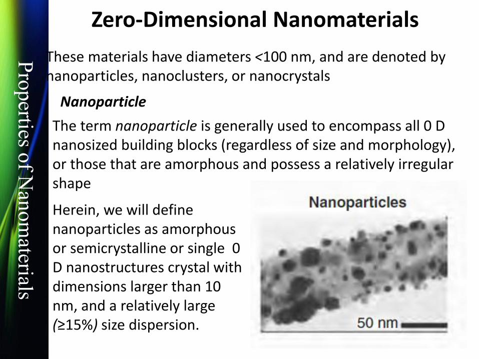
These materials have diameters <100 nm, and are denoted by nanoparticles, nanoclusters, or nanocrystals
The term nanoparticle is generally used to encompass all 0 D nanosized building blocks (regardless of size and morphology), or those that are amorphous and possess a relatively irregular shape
Herein, we will define nanoparticles as amorphous or semicrystalline or single 0 D nanostructures crystal with dimensions larger than 10 nm, and a relatively large (≥15%) size dispersion.
Nanoparticle
Pro
perties o
f Nan
om
aterials
For the fabrication of nanoparticles, a small size is not the only requirement. For any practical application, the processing conditions need to be controlled in such a way that resulting nanoparticles have the following characteristics: (i) identical size of all particles (also called monosized or with uniform size distribution) (ii) identical shape or morphology, (iii) identical chemical composition and crystal structure (iv) individually dispersed or monodispersed, i.e. no agglomeration. If agglomeration does occur, nanoparticles should be readily redispersible

Pro
perties o
f Nan
om
aterials

Pro
perties o
f Nan
om
aterials
The first 0D nanoarchitecture: the fullerenes
“Nanotechnology revolution” was catalyzed by the mid-1980s discovery of carbon nanoclusters known as fullerenes C60
The 1996 Nobel Prize in Chemistry was awarded to Richard Smalley, Robert Curl, and Sir Harold Kroto for this discovery
To date, the most common applications for fullerenes include MRI contrast agents (exploiting its container properties), drug-delivery agents (through surface functionalization), and light-activated antimicrobial Agents etc.

Pro
perties o
f Nan
om
aterials C60, containing alternating six- and five membered rings of sp2 hybridized carbon atoms. This is only one isomer for C60, out of a staggering total of 1,812 possible structures
Pro
perties o
f Nan
om
aterials
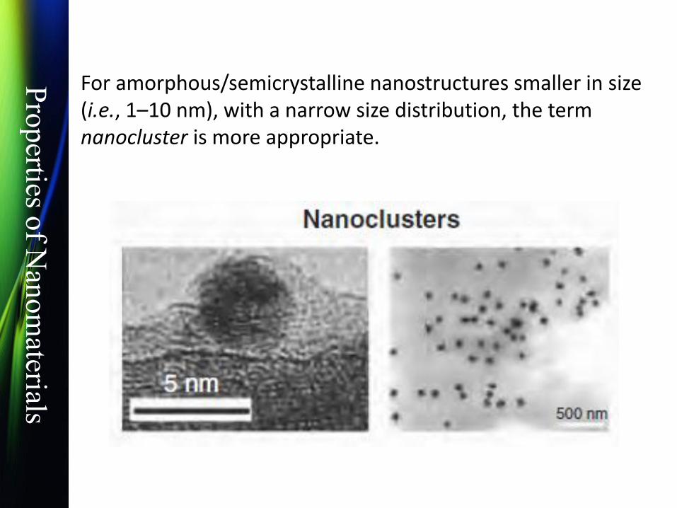
For amorphous/semicrystalline nanostructures smaller in size (i.e., 1–10 nm), with a narrow size distribution, the term nanocluster is more appropriate.
Pro
perties o
f Nan
om
aterials
It is also important here to note the difference between nanoparticles/nanoclusters and traditional colloids, which date back to the early 1860s
Term colloid, which is used to describe solid/liquid and solid/gas suspensions such as milk, paints, butter, smoke, and smog.
Although both types of materials have sizes within the nanoregime, the leading difference is the control one has over composition and morphology.
In order to stabilize metal nanostructures, a stabilizing agent must be used to prevent agglomeration into a larger powder. This is also the case for colloids, which generally employ polydispersed organic polymers and other ionic species that may adsorb to the colloid surface.

Pro
perties o
f Nan
om
aterials
Analogous to bulk materials, any nanomaterial that is crystalline should be referred to as a nanocrystal. This term should be reserved for those materials that are single crystalline; if a particle exhibits only regions of crystallinity, it is better termed a nanoparticle or nanocluster depending on its dimensions. Transmission electron microscopy, especially in tandem with electron diffraction is most useful in determining the crystallinity of any nanostructure
A special case of nanocrystal that is comprised of a semiconductor is known as a quantum dot.
Typically, the dimensions of these nanostructures lie in the range 1–30 nm, based on its composition Quantum dots currently find applications as sensors, lasers, and LEDs. In fact, new high-density disks (e.g., HD-DVD and Blu-ray high-definition DVD formats) may only be read via blue lasers, which are fabricated from quantum dots. Long-term applications for these structures will likely include optical computing and high-efficiency solar cells.

Pro
perties o
f Nan
om
aterials
TEM images of amorphous nanoclusters (a), and nanocrystals, (b). The inset of (a) shows selected area electron diffraction (SAED); the absence of a pattern indicates an amorphous structure. The scale bar is 20 nm. The high-resolution TEM image inset in (b) shows lattice spacings of an individual nanocrystal.
Pro
perties o
f Nan
om
aterials
when an electron is promoted from the valence to conduction bands, an electron–hole pair known as an exciton is created in the bulk lattice. The physical separation between the electron and hole is referred to as the exciton Bohr radius (rB) that varies depending on the semiconductor composition. In a bulk semiconductor crystal, rB is significantly smaller than the overall size of the crystal; hence, the exciton is free to migrate throughout the lattice
However, in a quantum dot, rB is of the same order of magnitude as the diameter (D) of the nanocrystal, giving rise to quantum confinement of the exciton. Empirically, this translates to the strongest exciton confinement when D ≤ 2rB.
Quantum dot

Pro
perties o
f Nan
om
aterials
Analogous to the “particle-in-a-box” model from introductory physical chemistry, exciton quantum confinement results in discrete energy levels rather than the continuous bands of a bulk semiconductor crystal. Since the gap between adjacent energy levels is infinitesimally small for a bulk semiconductor, the bandgap is considered as a fixed value. In contrast, since the dimensions of a quantum dot are extremely small, the addition/subtraction of a single atom will significantly change the nanocrystal dimensions and bandgap.
Table lists the rB values for common semiconductor crystals whose bandgap may be easily fine-tuned by simply changing the diameter of the quantum dot, as long as the dimensions are smaller than rB.

Pro
perties o
f Nan
om
aterials
In the early 1980s, Efros described the size-dependent electronic properties of quantum dots, first delineating that the bandgap, En, will increase from the bulk value based on a 1/R2 confinement energy term (Eq. 1). According to quantum confinement theory, electrons in the conduction band and holes in the valence band are spatially confined by the potential barrier of the surface. Due to confinement of both electrons and holes, the lowest energy optical transition from the valence to conduction band will increase in energy, effectively increasing the bandgap.
where Eg is the bandgap of the bulk semiconductor; h, Planck’s constant; R, the radius of the quantum dot; and μ is mass of the exciton given by memh/(me +mh). Here me and mh are masses of the electron and hole, respectively

Pro
perties o
f Nan
om
aterials
where ER is the Rydberg (spatial correlation) energy of bulk semiconductor:
where ε0 is the permittivity of free space; ε, the dielectric constant of the bulk semiconductor; and me is the mass of the electron. Hence, the absorption energy of quantum dots will shift to higher frequency with decreasing diameter of the dots, with a dependence of 1/R2.

Pro
perties o
f Nan
om
aterials
Synthesis of metallic and oxide nanoparticles
Reduction of metal complexes in dilute solutions is the general method in the synthesis of metal colloidal dispersions, and a variety of methods have been developed to initiate and control the reduction reactions.
In the synthesis of metallic nanoparticles, or more specifically speaking, metallic colloidal dispersion, various types of precursors, reduction reagents, other chemicals, and methods were used to promote or control the reduction reactions
Colloidal dispersion of rhodium by refluxing a solution of
rhodium chloride and PVA in a mixture of methanol and water
at 79°C. Here, methanol was used as a reduction reagent
Commonly oxide particles in colloidal dispersions are
synthesized by sol-gel processing.

Pro
perties o
f Nan
om
aterials
One-Dimensional Nanostructures
Referred to as 1D nanostructures, is reserved for those materials that have nanoscale dimensions that are equivalent in all but one direction.
The common thread among all of these structures is that their diameters must be within the 1–100 nm range; typically, their lengths are within the micron (or larger) regime.
Nanotube, Nanofiber, Nanowire, and Nanorod

Pro
perties o
f Nan
om
aterials
Carbon nanotubes
The most widely studied 1D nanomaterial is the carbon nanotube (CNT). These structures were first discovered by Iijima in 1991, and consist of a graphitic sheet(s) rolled into a tubular array. Based on the layers of graphene sheets that comprise the CNT, the structures are designated as single-walled, double-walled, or multiwalled nanotubes (SWNTs, DWNTs, or MWNTs respectively)
Pro
perties o
f Nan
om
aterials
TEM images of MWNTs, formed from the folding (a) 5-, (b) 2-
(i.e., DWNT), and (c) 7- stacked graphene sheets.
Pro
perties o
f Nan
om
aterials
The diameters of CNTs range from 1 nm (SWNTs) to >30 nm (MWNTs), with aspect ratios (length:width) ranging from 100 to greater than 1 × 10⁶ . Even though the diameters of CNTs are orders of magnitude smaller than a human hair, their tensile strength is ca. 20 times greater than steel – a property attributed to extremely strong sp2 bonding between neighboring hexagonal units.
The electrical conductivity of SWNTs may vary from metallic to semiconducting, depending on the way a graphene sheet is folded
For metallic SWNTs, the electrical conductance may exceed silver or copper by three orders of magnitude.
Pro
perties o
f Nan
om
aterials
metallic
semiconducting

Pro
perties o
f Nan
om
aterials
Since CNTs have a high electrical conductivity and contain sharp tips, these nanomaterials are the best-known field emitter.
In general, the smaller the radius of curvature of the tip, the more concentrated the electric field will be, which corresponds to increased field emission at low required voltages. This property is currently being exploited for the design of flat-panel field emission displays.
Though plasma and LCD displays are hot ticket items at electronics stores, they both possess inherent disadvantages. Plasma displays are extremely heavy, consume a significant amount of energy, and are prone to “burn-in,” which permanently degrades the screen. On the other hand, LCD screens are expensive to produce and often lack the response time required to view fast-paced sporting events/movies without blur.
Pro
perties o
f Nan
om
aterials
Hence, as far as picture quality is concerned, traditional CRT displays are still among the finest quality. The replacement of this technology with CNTs is a logical step in the evolution of display panels. Rather than a single electron gun, CNT-based screens will contain a separate nanotube electron gun for each individual pixel in the display – dramatically enhancing the resolution and clarity of the picture. Further, in contrast to current large flat-panel televisions, the overall weight of CNT-based analogues will be significantly lower, and they will consume far less power.

Pro
perties o
f Nan
om
aterials
A nanotube is a 1D structure that contains a hollow core, whereas the other three nanoarchitectures are solid throughout.
MnO2 nanotube arrays

Pro
perties o
f Nan
om
aterials
A nanorod is typically a crystalline 1D nanostructure, with an overall length comparable to its width (i.e., both dimensions are <100 nm). As their name implies, another feature of nanorods is their rigid sidewall structures. The term “nanocrystal” is probably more appropriate for these structures (or, more explicitly: “rod-like nanocrystals”).
Whereas nanowires, nanofibers, and nanotubes exhibit an interwoven array, nanorods are completely linear in morphology. As such, nanorods are capable of stacking onto each other to yield interesting 2D and 3D arrays
SEM pictures of
ZnO nanorods
on sapphire
substrate (A)
and SiO2
substrate (B)
Nanorods
Pro
perties o
f Nan
om
aterials
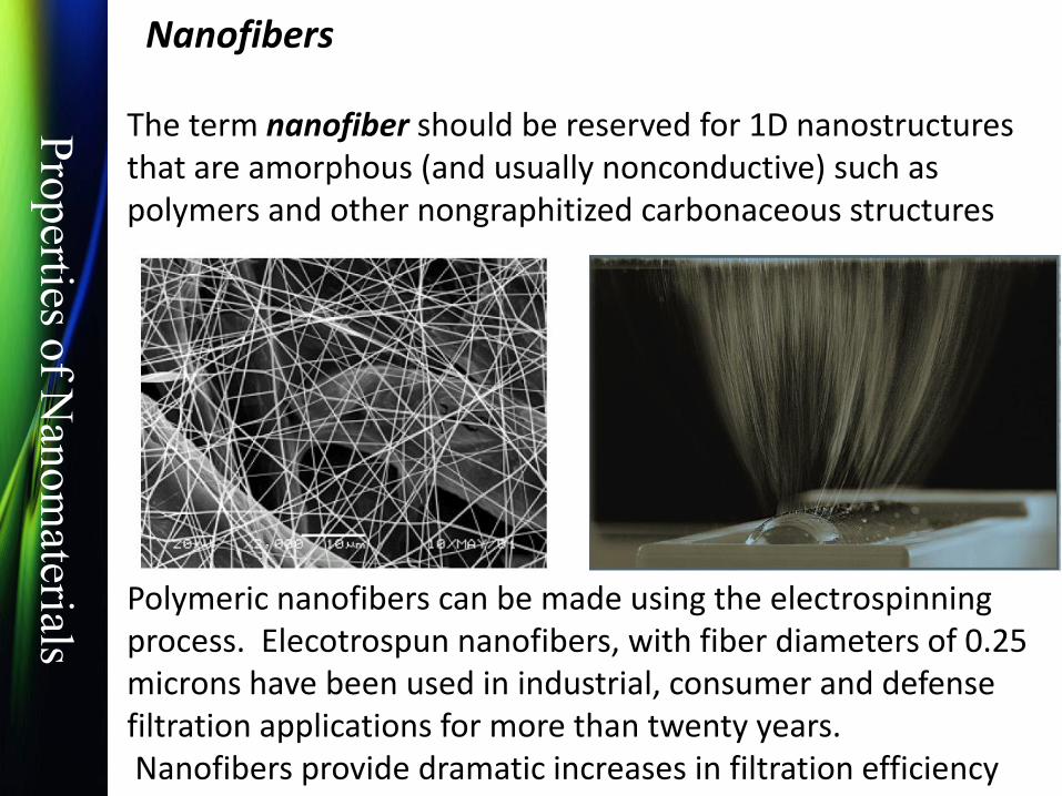
The term nanofiber should be reserved for 1D nanostructures that are amorphous (and usually nonconductive) such as polymers and other nongraphitized carbonaceous structures
Polymeric nanofibers can be made using the electrospinning process. Elecotrospun nanofibers, with fiber diameters of 0.25 microns have been used in industrial, consumer and defense filtration applications for more than twenty years. Nanofibers provide dramatic increases in filtration efficiency
Nanofibers
Pro
perties o
f Nan
om
aterials
2Dimentional Nano Structured Materials 2D nanostructures have two dimensions outside of the nanometric size range. In recent years, a synthesis 2D NSMs have become a focal area in materials research, owing to their many low dimensional characteristics different from the bulk properties. In the quest of 2D NSMs, considerable research attention has been focused over the past few years on the development of 2D NSMs. 2D NSMs with certain geometries exhibit unique shape-dependent characteristics and subsequent utilization as building blocks for the key components of nanodevices

Pro
perties o
f Nan
om
aterials
SEM image of Bi2WO6 nanoplates

Pro
perties o
f Nan
om
aterials
SEM and TEM images of ZnO nanodisks

Pro
perties o
f Nan
om
aterials
3 Dimentional Nano Structured Materials
It is of great interest to synthesize 3D NSMs with a controlled structure and morphology. In addition, 3D nanostructures are an important material due to its wide range of applications in the area of catalysis, magnetic material and electrode material for batteries. Moreover, the 3D NSMs have recently attracted intensive research interests because the nanostructures have higher surface area and supply enough absorption sites for all involved molecules in a small space . On the other hand, such materials with porosity in three dimensions could lead to a better transport of the molecules
nanoballs (dendritic structures), nanocoils, nanocones, nanopillers and nanoflowers

Pro
perties o
f Nan
om
aterials
3D urchin-like nanostructured AlN
Pro
perties o
f Nan
om
aterials
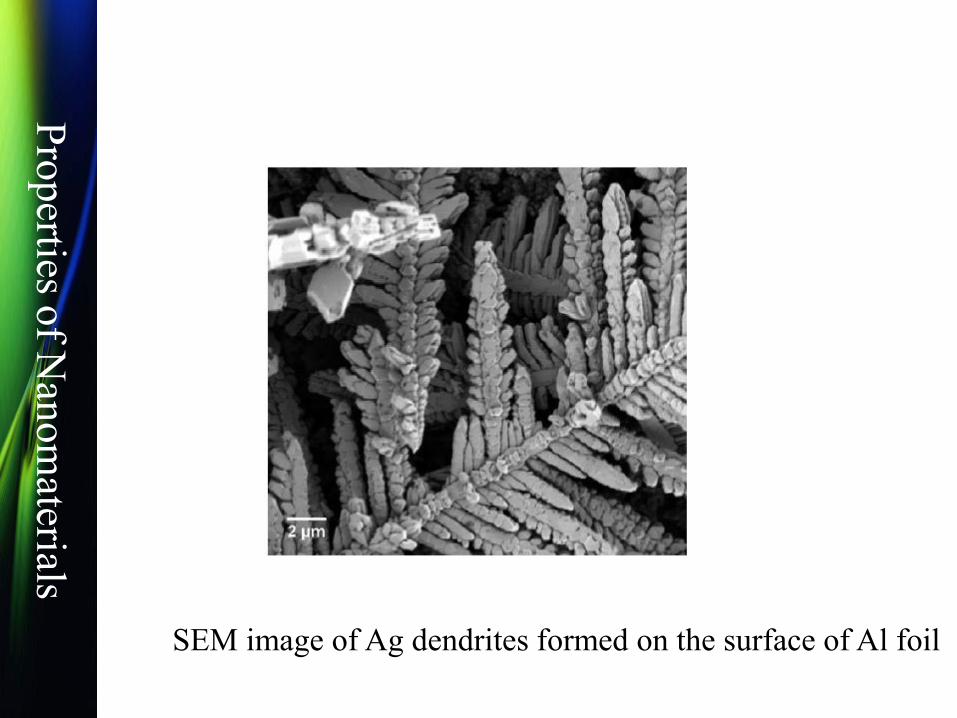
SEM image of Ag dendrites formed on the surface of Al foil

Pro
perties o
f Nan
om
aterials
Low-magnification SEM images of 3D crystalline
TiO2 nanostructures

Pro
perties o
f Nan
om
aterials
Analogous to bulk materials, the agglomeration of noncrystalline nanostructural subunits should best be termed a nanopowder
Nanopowder

Pro
perties o
f Nan
om
aterials
Many techniques have been developed in the
synthesis and formation of one-dimensional
nanostructured materials
These techniques can be generally grouped into four
(1) Spontaneous growth:
(a) Evaporation-condensation
(b) Vapor (or solution)–liquid–solid (VLS or SLS) growth
(2) Template-based synthesis:
(a) Electroplating
(b) Colloid dispersion, melt, or solution filling
(3) Electrospinning
(4) Lithography
Pro
perties o
f Nan
om
aterials
Spontaneous growth and template-based synthesis are considered as a bottom-up approach, whereas lithography is a top-down technique. Spontaneous growth commonly results in the formation of single crystal nanowires or nanorods along a preferential crystal growth direction depending on the crystal structures and surface properties of the nanowire materials. Template-based synthesis mostly produces polycrystalline or even amorphous products
Pro
perties o
f Nan
om
aterials
Evaporation (dissolution)-condensation growth
Evaporation-condensation process is also referred to as
a vapor–solid (VS) process
Nanowires and nanorods grown by evaporation-condensation
methods are commonly single crystals with fewer imperfections.
The formation of nanowires, nanorods or nanotubules through
evaporation (or dissolution)-condensation is due to the
anisotropic growth.
Pro
perties o
f Nan
om
aterials
In a VLS growth, the process can be simply described as
following
The growth species is evaporated first, and then diffuses and
dissolves into a liquid droplet. The surface of the liquid has a
large accommodation coefficient, and is therefore a preferred
site for deposition. Saturated growth species in the liquid
droplet will diffuse to and precipitate at the interface between
the substrate and the liquid. The precipitation will follow first
nucleation and then crystal growth.
Continued precipitation or growth will separate the substrate
and the liquid droplet, resulting in the growth of nanowires.

Pro
perties o
f Nan
om
aterials Schematic showing the principal steps of the vapor–
liquid–solid growth technique: (a) initial nucleation
and (b) continued growth

Pro
perties o
f Nan
om
aterials
Example the VLS growth
A thin layer of gold is sputtered on a silicon substrate and
annealed at an elevated temperature (above the eutectic point
of 385 C of the silicon–gold system), which is typically the same
as the growth temperature.
During the annealing, silicon and gold react and form a liquid
mixture, which forms a droplet on the silicon substrate surface.
When silicon species is evaporated from the source and
preferentially condensed at the surface of the liquid droplet, the
liquid droplet will become supersaturated with silicon.
Subsequently, the supersaturated silicon will diffuse from
the liquid–vapor interface to and precipitate at the solid–liquid
interface

Pro
perties o
f Nan
om
aterials
The size of nanowires grown by VLS method is solely
determined by the size of the liquid catalyst droplets. To
grow thinner nanowires, one can simply reduce the size of
the liquid droplets. Typical method used to form
small liquid catalyst droplets is to coat a thin layer of catalyst
on the growth substrate and to anneal at elevated temperatures
Control of the size of nanowires

Pro
perties o
f Nan
om
aterials
Synthesis of 3D NSMs by physical processes In recent
years, with the progress of nanotechnology, there has
been increasing interest in the synthesis of 3D NSMs (for
instance spring-like nanocoils, ball-like nanodendritic
structures, and nanoflowers) because they are exhibit
newer and/or better physical/chemical properties.
Concerning the fabrication of these nanoarchitectures,
evaporation technique, sputtering technique, lithography
process, hot plasma, cold plasma, spray pyrolysis, inert
gas phase condensation technique,

Pro
perties o
f Nan
om
aterials
3D graphitic nanosheets using CVD in the presence of
methane gas
(A) SEM and (B) AFM images of the 3D graphitic nanosheets.
Pro
perties o
f Nan
om
aterials
Metallic nanoparticles possess unique optical, electronic, chemical and magnetic properties that are strikingly different from that of the individual atoms as well as their bulk counterparts . Various physical properties, such as, mechanical strength, ductility, thermal stability, sintering ability, diffusivity and the chemical reactivity of the particles in the nanometer regime have also been found to be dependent on particle size without a change in the chemical composition of the particles.
Metallic nanoparticles

Pro
perties o
f Nan
om
aterials
In a metal cluster, atoms at surfaces have fewer neighbours than atoms in the bulk. As a result, the atoms in the bulk are co-ordinatively saturated while the atoms on the surface are co-ordinatively unsaturated. Because of this lower coordination and unsatisfied bonds, surface atoms are less stabilised than bulk atoms. The smaller a particle, the larger the fraction of atoms at the surface and the higher the average binding energy per atom. One distinguishing characteristic of nanometer scale structures is that unlike macroscopic materials, they typically have a high percentage of their constituent atoms at the surface.
Pro
perties o
f Nan
om
aterials
The volume of an object (Vα R3, where R is the characteristic length) decreases more quickly than its surface area (S αR2) as the size diminishes: S/V α R-1, where R has atomic or molecular dimensions. This scaling behavior leads, in the most extreme case, to structures where nearly every atom in the structure is interfacial and in some sense, it could be assumed that nanostructures are “all surface”. The term ‘surface’ has been used to indicate the geometrical separation between two or more phases of matter whereas the term ‘interface’ implies a region of finite thickness over which the phase change occurs

Pro
perties o
f Nan
om
aterials
Another important aspect is the electronic structure of the nanoparticles that depends critically on the size of the particles. In metals and semiconductors, the electronic wavefunctions of conduction electrons are delocalised over the entire particle. Electrons can, therefore, be described as ‘particles in a box’ and the densities of state and the energies of the particles depend crucially on the size of the box which, at the onset, leads to a smooth size dependence.
Pro
perties o
f Nan
om
aterials
The HOMO– LUMO band gap of semiconductor particles and therefore, their absorption and fluorescence wavelengths become size dependent
Ionisation potentials and electron affinities are tuned between the atomic values and the work function of the bulk material by variation of the cluster size. These properties relate to the availability of electrons for forming bonds or getting involved in redox reactions and thus, the catalytic activity and selectivity also become functions of size
Pro
perties o
f Nan
om
aterials
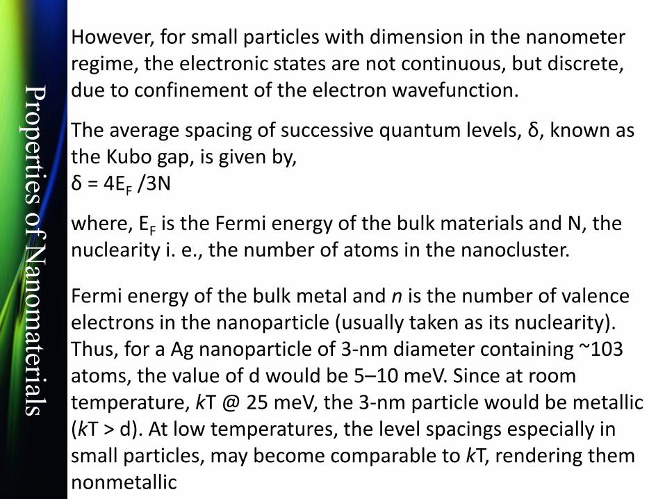
However, for small particles with dimension in the nanometer regime, the electronic states are not continuous, but discrete, due to confinement of the electron wavefunction.
The average spacing of successive quantum levels, δ, known as the Kubo gap, is given by, δ = 4EF /3N
where, EF is the Fermi energy of the bulk materials and N, the nuclearity i. e., the number of atoms in the nanocluster.
Fermi energy of the bulk metal and n is the number of valence electrons in the nanoparticle (usually taken as its nuclearity). Thus, for a Ag nanoparticle of 3-nm diameter containing ~103 atoms, the value of d would be 5–10 meV. Since at room temperature, kT @ 25 meV, the 3-nm particle would be metallic (kT > d). At low temperatures, the level spacings especially in small particles, may become comparable to kT, rendering them nonmetallic

Pro
perties o
f Nan
om
aterials
Named after the Japanese theoretical physicist, Roygo Kubo introduced the concept in 1962. The Kubo gap is the average spacing that exists between consecutive energy levels and measured in the units of millielectron volts (meV). Since, the number of valence electrons in the nanoparticles is measured as a function of nuclearity, the energy level spacing varies inversely with the nuclearity of the particles

Pro
perties o
f Nan
om
aterials Evolution of the band gap and the density of states as the number of atoms in a system increases

Pro
perties o
f Nan
om
aterials
In band theory, the breadth of a band is directly related to the strength of interactions among nearest neighbours. For atoms/molecules, this interaction is weak which corresponds to a narrow band.
Additional atoms are added to the solid, stronger interactions will occur resulting in a greater density of states near the Fermi level.
Hence, the insulating properties of very small nanoclusters are due to the small number of neighboring atoms which are held together primarily by non-metallic interactions (e.g., van der Waal forces). As size of the nanocluster increases, the atomic s/p and d orbitals from a larger number of constituent atoms will broaden into bands forming an energy continuum

Pro
perties o
f Nan
om
aterials
Theoretical investigations of the electronic structure of metal nanoparticles gold clusters with N = 6,……,147 also throw light on the size-induced changes in the electronic structure.
The HOMO-LUMO gap decreases with particle size from 1.8 eV for Au6 to 0.3 eV for Au147.
The Kubo gap has dramatic effect on the properties associated with the material. It is possible to control the Kubo gap which will, then, cause the system to become metallic or non-metallic.

Pro
perties o
f Nan
om
aterials
Atoms have their well known atomic orbitals. Depending on the extent of overlap in a solid they remain mostly unperturbed, as in noble gases, or they combine to extended band structures, as in metals or semiconductors. The core orbitals are confined to a relatively small volume and remain localised (atom-like). Each of N atoms contributes with its atomic states to a band so that, although the width of a band increases slightly when more atoms are added, the density of states (DOS) within a band is basically proportional to the number of atoms of an ensemble with an extended band-like state. The band width amounts typically to a few eV. Thus, the DOS is on the order of N per eV, which is very large for a bulk amount of matter (N # Avogadro’s number, NA) but low for small clusters.
Pro
perties o
f Nan
om
aterials
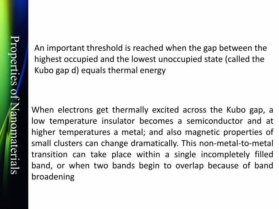
An important threshold is reached when the gap between the highest occupied and the lowest unoccupied state (called the Kubo gap d) equals thermal energy
When electrons get thermally excited across the Kubo gap, a low temperature insulator becomes a semiconductor and at higher temperatures a metal; and also magnetic properties of small clusters can change dramatically. This non-metal-to-metal transition can take place within a single incompletely filled band, or when two bands begin to overlap because of band broadening

Pro
perties o
f Nan
om
aterials
Temperature dependence of the resistivity for nanostructured Nb films with different grain sizes (dXRD). The scale on the left refers to the metallic films with dXRD 8 nm while the scale on the right is for the insulating films with dXRD < 8 nm. Particle size dependence of the resistivity at 10 and 300 K, depicted, respectively, by open triangles and circles.
High resolution transmission electron micrographs of the nanostructured Nb sample with dXRD ≈ 5 nm. The grains are defined as crystallographically ordered regions (delineated in the figure) while the disordered inter-granular regions are ≈1 nmwide.
Pro
perties o
f Nan
om
aterials
The creation, processing, characterization, and
utilization of materials, devices, and systems with
dimensions on the order of 0.1–100 nm, exhibiting
novel and significantly enhanced physical,
chemical, and biological properties, functions,
phenomena, and processes due to their nano-
scale size’’ .
Current interests in nanotechnology
encompass nano-biotechnology, nano-systems,
nano-electronics, and nano-structured materials,
of which nanocomposites are a significant parti
Nanocomposites
Pro
perties o
f Nan
om
aterials
The expansion of length scales from meters (finished
woven composite parts), micrometers (fiber diameter),
sub-micrometers (fiber/matrix interphase) to nanome-
ters (nanotube diameter) presents tremendous
opportu-nities for innovative approaches in the
processing, characterization, and analysis/modeling of
this new gen-eration of composite materials.
Pro
perties o
f Nan
om
aterials
Constituents have at least one dimension in
the nanometer scale.
Nanoparticles (Three nano-scale dimensions)
Nanofibers (Two nano-scale dimensions)
Nanoclays (One nano-scale dimensions)
Pro
perties o
f Nan
om
aterials
Nanoparticle-reinforced composites
Particulate composites reinforced with micron-sized particles of various
materials are perhaps the most widely utilized composites in everyday
materials. Particles are typically added to enhance the matrix elastic
modulus and yield strength. By scaling the particle size down to the
nanometer scale, it has been shown that novel material properties can be
obtained
Micron-scale particles typically scatter light making otherwise
transparent matrix materials appear opaque. showed in their
study of SiO2/epoxy composites that decreasing the particle size
resulted in significantly improved transmittance of visible light.

Pro
perties o
f Nan
om
aterials
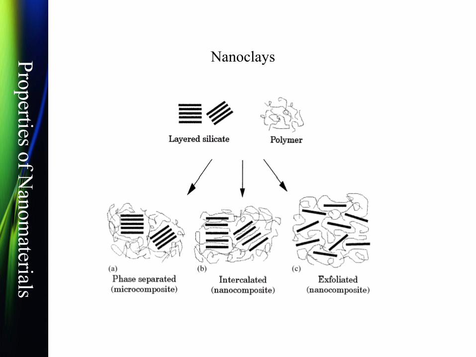
Nanoplatelet-reinforced composites
Clay and graphite. In their bulk state, both clay and
graphite exist as layered materials. In order to utilize these
materials most efficiently, the layers must be separated and
dispersed throughout the matrix phase.
The advantages of polymer-based clay nano-composites
include improved stiffness, strength, tough-ness, and thermal
stability as well as reduced gas permeability and coefficient of
thermal expansion
In addition to mechanical properties, the thermal sta-bility, fire
resistance and gas barrier properties of poly-mer/clay
nanocomposites can be enhanced through the addition of
nanometer-scale reinforcement.
Pro
perties o
f Nan
om
aterials
Nanoclays

Pro
perties o
f Nan
om
aterials
Nanofiber-reinforced composites
Vapor grown carbon nanofibers (CNF) have been
used to reinforce a variety of polymers, including poly-
propylene, polycarbonate, nylon, and epoxy.
Carbon nanofibers are known to have wide-ranging
morphologies, from structures with a disordered bamboo-
like structure to highly graph-itized ‘‘cup stacked’’
structures
Carbon nanofibers typically have diameters on the order of 50–200 nm
Pro
perties o
f Nan
om
aterials
Researchers utilized a variety of techniques to
achieve dispersion of carbon nanofibers in a poly(ethylene
terephthalate) (PET) matrix and subsequently melt-spun
fibers. The compressive strength and torsional moduli of the
nanocomposite fibers were considerably higher than that for
the unreinforced PET fiber

Pro
perties o
f Nan
om
aterials
Carbon nanotube-reinforced composites
The density of a SWCNT is about 1.33–1.40 g/cm3
, which is just one-half of the density of aluminum. The elastic
modulus of SWCNT is comparable to that of diamond
(1.2 TPa). The reported tensile strength of SWCNT is much
higher than that of high-strength steel (2 GPa). The
tremendous resilience of SWCNT in sustaining bending to
large angles and restraightening without damage is
distinctively different from the plastic defor-mation of metals
and brittle fracture of carbon fibers at much lower strain when
subjected to the same type of deformation.
Pro
perties o
f Nan
om
aterials
The electric current carrying capability is estimated to be 1·10
9 amp/cm 2 , whereas copper wires burn out at about 1·10
6 amp/cm 2 . The thermal conductivity of SWCNT is predicted
to be 6000 W/ m K at room temperature; this is nearly double
the ther-mal conductivity of diamond of 3320 W/m K.
SWCNTs are stable up to 2800�C in vacuum and 750�C in air,
whereas metal wires in microchips melt at 600–1000 �C.
SWCNTs have great potential in field emission applications
because they can activate phosphors at 1– 3 V if electrodes are
spaced 1lm apart. Traditional Mo tips require fields of 10–100
V/lm and have very limited lifetimes.

Pro
perties o
f Nan
om
aterials
The outstanding thermal and electric properties com-bined
with their high specific stiffness and strength, and
very large aspect ratios have stimulated the development
of nanotube-reinforced composites for both structural
And functional application

Pro
perties o
f Nan
om
aterials
Both SWCNTs and MWCNTs have been utilized for
reinforcing thermoset polymers (epoxy, polyimide, and
phenolic), as well as thermoplastic polymers (polypro-
pylene, polystyrene, poly methyl methacrylate (PMMA),
nylon 12 etc.
Researchers fabricated nanocomposites consisting of DWCNTs
with a high degree of dispersion The resulting composites
showed increase of strength, Young� s modulus and strain to
failure at a nanotube con-tent of only 0.1 wt%. In addition, the
nanocomposites showed significantly enhanced fracture
toughness as compared to the unreinforced epoxy..
Pro
perties o
f Nan
om
aterials
In the processing of nanocomposites, carbon nano-tubes need
to be separated from bundles and dispersed uniformly in a
polymer matrix for maximizing their contact surface area
with the matrix. Modification of nanotube surfaces, for
example, the creation of cova-lent chemical bonds between
nanotubes and the poly-mer matrix, enhances their
interactions and gives rise to higher interfacial shear strength
than van der Waals bonds.
Pro
perties o
f Nan
om
aterials
Critical issues in nanocomposites
There is a lack of understanding of the interfacial
bonding between the reinforcements and the matrix
material from both analytical and experimental
viewpoints
Dispersion
Uniform dispersion of nanoparticles, and nanotubes
against their agglomeration due to van der Waals bond-ing is
the first step in the processing of nanocomposites.
Beside the problems of agglomeration of nanoparticles,
exfoliation of clays and graphitic layers are essential.
SWCNTs tend to cluster into ropes and MWCNTs pro-duced
by chemical vapor deposition are often tangled
together like spaghettis. The separation of nanotubes
in a solvent or a matrix material is a prerequisite for
aligning them.

Pro
perties o
f Nan
om
aterials
Alignment
Because of their small sizes, it is exceedingly
difficult to align the nanotubes in a polymeric
matrix material in a manner accomplished in
traditional short fiber com posites. The lack of
control of their orientation dimin-ishes the
effectiveness of nanotube reinforcement in
composites, whether for structural or functional
performance.

Pro
perties o
f Nan
om
aterials
Volume and rate
High volume and high rate fabrication is fundamen-
tal to manufacturing of nanocomposites as a commer-
cially viable product. The lessons learned in the
fabrication of traditional fiber composites have clearly
demonstrated that the development of a science base
for manufacturing is indispensable. Efficiency in
manu-facturing is pivotal to the future development of
nanocomposites
Pro
perties o
f Nan
om
aterials
Cost effectiveness
Besides high volume andhigh rate production, the cost
of nanocomposites also hinges on that of the nano-
reinforcement material, particularly, nanotubes. It is
anticipated that as applications for nanotubes and their
composites increase the cost will be dramatically
reduced
Pro
perties o
f Nan
om
aterials
Size dependent absorption spectra

Pro
perties o
f Nan
om
aterials
UV-visible absorption spectroscopy probes electronic transitions
due to electronic excited states
Pro
perties o
f Nan
om
aterials
Some Applications
Detection of Impurities
UV absorption spectroscopy is one of the best methods for determination of
impurities in organic molecules. Additional peaks can be observed due to
impurities in the sample and it can be compared with that of standard raw
material. By also measuring the absorbance at specific wavelength, the impurities
can be detected.
Structure elucidation of organic compounds.
UV spectroscopy is useful in the structure elucidation of organic molecules.
It is rarely used as a primary method for structure determination

Pro
perties o
f Nan
om
aterials
Quantitative analysis
UV absorption spectroscopy can be used for the quantitative determination
of compounds that absorb UV radiation.
Qualitative analysis
UVabsorption spectroscopy can characterize those types of compounds
which absorbs UV radiation. Identification is done by comparing the
absorption spectrum with the spectra of known compounds.
Chemical kinetics
Kinetics of reaction can also be studied using UV spectroscopy. The
UV radiation is passed through the reaction cell and the absorbance
changes can be observed.
Band Gap determination
Particle size determination

Pro
perties o
f Nan
om
aterials
Transition between two electronic energy levels should give
rise to a line in an absorption.
In practice, it may not be possible to distinguish individual
line.
Large molecules have large number of vibrational and
rotational levels. These energy levels may be close together.
UV-vis radiation may rise molecules at many slightly
different electronic energy levels to many slightly different
higher levels.
As a result sharp lines are replaced by narrow bands
Pro
perties o
f Nan
om
aterials
Blue Shift
Nanosized semiconductor particles generally exhibit a threshold energy in the
optical absorption measurements, due to the size specific band gap structures,
which is reflected by the blue shifting of the absorption edge (from near-infrared
to visible) with decreasing particle size
A convenient method of characterizing the size and size distribution of
semiconductor nano-particles is UV/Visible absorption spectroscopy
Semiconductor nano- crystallites are know to have an absorption edge, which is
shifted with respect to the bulk materials towards shorter wavelengths
Pro
perties o
f Nan
om
aterials

Pro
perties o
f Nan
om
aterials
Pro
perties o
f Nan
om
aterials
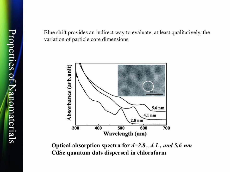
Blue shift provides an indirect way to evaluate, at least qualitatively, the
variation of particle core dimensions
Optical absorption spectra for d=2.8-, 4.1-, and 5.6-nm
CdSe quantum dots dispersed in chloroform

Pro
perties o
f Nan
om
aterials
UV-Vis absorption spectra for ZnO nanoparticles.
Pro
perties o
f Nan
om
aterials

Pro
perties o
f Nan
om
aterials
An exciton is a bound state of an electron and hole which are attracted to each other by
the electrostatic Coulomb force. It is an electrically neutral quasiparticle that exists in
insulators, semiconductors and some liquids. The exciton is regarded as an elementary
excitation of condensed matter that can transport energy without transporting net
electric charge
An exciton forms when a photon is absorbed by a semiconductor. This excites an electron
from the valence band into the conduction band. In turn, this leaves behind a localized
positively-charged hole. The electron in the conduction band is then attracted to this
localized hole by the Coulomb force. This attraction provides a stabilizing energy balance.
Consequently, the exciton has slightly less energy than the unbound electron and hole.

Pro
perties o
f Nan
om
aterials
Size distribution
If there is a very narrow size distribution, the first exciton peak will be
very sharp. This is because due to the
narrow size distribution, the differences in band gap between different
sized particles will be very small and hence most of the electrons will get
excited over a smaller range of wavelengths

Pro
perties o
f Nan
om
aterials
Silver Nanoparticles
Pro
perties o
f Nan
om
aterials
In metal nano particles such as in silver, the conduction band and
valence band lie very close to each other in which electrons move
freely. These free electrons give rise to a surface plasmon resonance
(SPR) absorption band occurring due to the collective oscillation of
electrons of silver nano particles in resonance with the light wave
Classically, the electric field of an incoming wave induces a polarization
of the electrons with respect to much heavier ionic core of silver
nanoparticles. As a result a net charge difference occurs which in turn
acts as a restoring force. This creates a dipolar oscillation of all the
electrons with the same phase.
Pro
perties o
f Nan
om
aterials
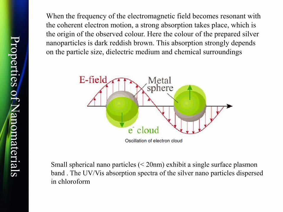
When the frequency of the electromagnetic field becomes resonant with
the coherent electron motion, a strong absorption takes place, which is
the origin of the observed colour. Here the colour of the prepared silver
nanoparticles is dark reddish brown. This absorption strongly depends
on the particle size, dielectric medium and chemical surroundings
Small spherical nano particles (< 20nm) exhibit a single surface plasmon
band . The UV/Vis absorption spectra of the silver nano particles dispersed
in chloroform
Pro
perties o
f Nan
om
aterials
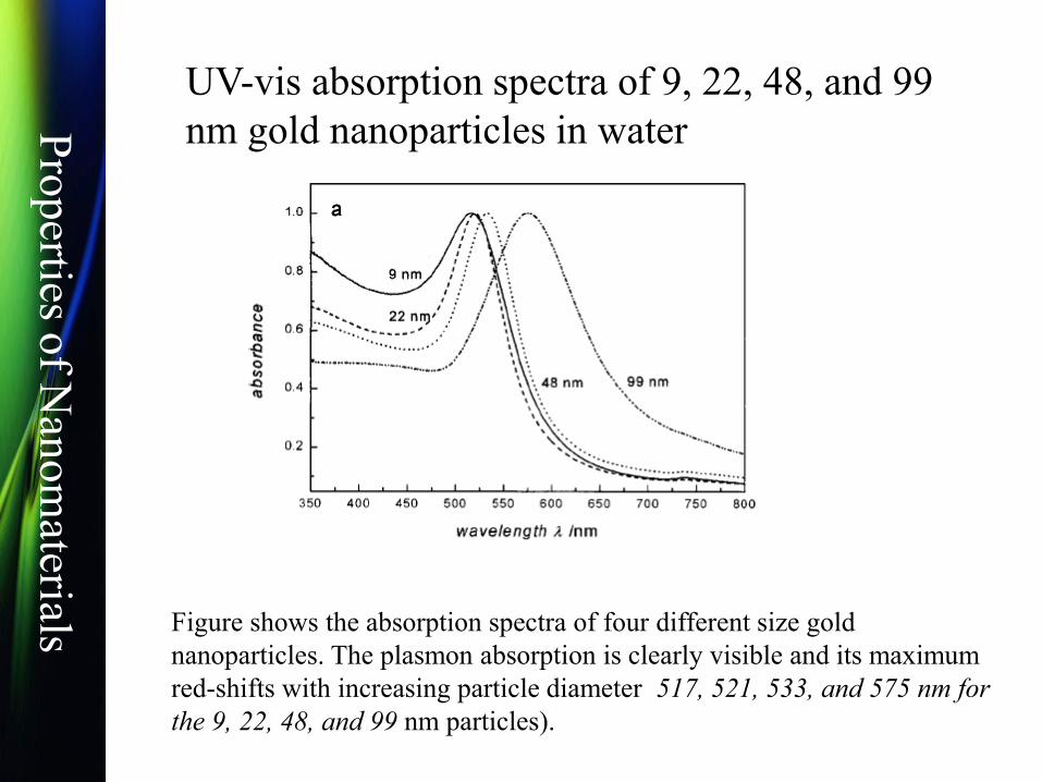
UV-vis absorption spectra of 9, 22, 48, and 99
nm gold nanoparticles in water
Figure shows the absorption spectra of four different size gold
nanoparticles. The plasmon absorption is clearly visible and its maximum
red-shifts with increasing particle diameter 517, 521, 533, and 575 nm for
the 9, 22, 48, and 99 nm particles).

Pro
perties o
f Nan
om
aterials
400 600 800 10000.0
0.2
0.4
0.6
0.8
Absorb
ance (
arb
. unit)
Wavelength (nm)
Size(nm) Ab. Peak Gr. time
6 700 nm 8 min
5.2 679 nm 4 min
4.7 665 nm 3 min
4.2 643 nm 2 min
2 531 nm 5 sec
Bulk
Absorption spectra of cadmium telluride
semiconductor nanocrystals including Bulk
Pro
perties o
f Nan
om
aterials
Phonons in Nanostructures

Pro
perties o
f Nan
om
aterials
Phonons are the principal carriers of thermal energy
in semiconductors and insulators, and they serve a
vital role in dissipating heat produced by scattered
electrons in semiconductor devices
Phonons are present in any material. They are the
driving forces for quite a number of phenomena
mentioning only the thermal expansion, heat
conductivity, temperature dependence of mechanical,
electric properties, phase transitions. They also enhance
the diffusion. They occur in bulk crystals, surface,
interfaces, multilayers, crystals with topological defects
and impurities.
Pro
perties o
f Nan
om
aterials
Unlike static lattice model , which deals with average positions of atoms in a
crystal, lattice dynamics extends the concept of crystal lattice to an array of
atoms with finite masses that are capable of motion. This motion is not random
but is a superposition of vibrations of atoms around their equilibrium sites due to
the interaction with neighbor atoms.
A collective vibration of atoms in the crystal forms a wave of allowed
wavelength and amplitude.
What are Phonons?
Just as light is a wave motion that is considered as composed of
particles called photons, we can think of the normal modes of vibration
in a solid as being particle-like. Quantum of lattice vibration is called
the phonon.
Phonon dispersion
The problem of lattice dynamics (LD) is to find the normal modes of vibration
of a crystal. In other words, LD seeks to calculate the energies (or frequencies
) of the phonons as a function of their wave vector's q . The relationship
between energy and q is called phonon dispersion .

Pro
perties o
f Nan
om
aterials
Two possible modes of vibrations of atoms in the crystal
Longitudinal
Transverse
In case of longitudinal mode the displacement of atoms from
their equilibrium position coincides with the propagation
direction of the wave
In the case of transverse mode, atoms move perpendicular to
the propagation of the wave.
Pro
perties o
f Nan
om
aterials
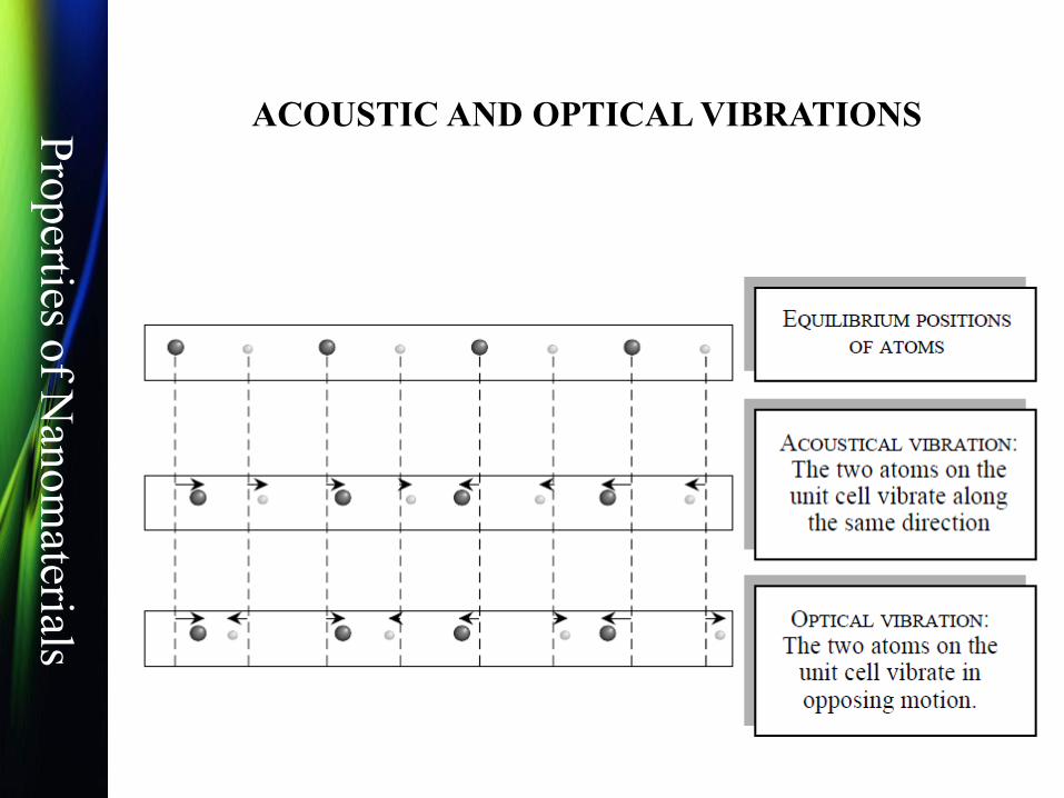
ACOUSTIC AND OPTICAL VIBRATIONS

Pro
perties o
f Nan
om
aterials
The difference between acoustical and optical branches
arises because of the more options of vibrations for atoms in
the unit cell. For example, atoms A and B of diatomic cell
can move together in phase (acoustical branch) or out of
phase (optical branch).

Pro
perties o
f Nan
om
aterials
In a simple mono atomic solid with only one atom per primitive
cell , one can have only three acoustic phonon branches
corresponding to the three degrees of freedom of atomic motion.
On the other hand, for monoatomic solids with two atoms per
primitive cell such as diamond, magnesium, or diatomic
compounds such as GaAs, one also has three optic phonon
branches in addition to the three acoustic phonons
In compounds with a greater number of atoms and complex
crystal structures, the number of optic phonons is more than
three.
If the crystal unit cell contains N atoms, then 3N degrees of
freedom result in 3 acoustic phonons and 3N − 3 optical
phonons.
ACOUSTIC AND OPTICAL BRANCHES

Pro
perties o
f Nan
om
aterials
These phonons can propagate in the lattice of a single crystal as
a wave and exhibit dispersion depending on their wavelength
or equivalently their wavevector
Phonon propagation is interrupted when a grain boundary is
encountered in a polycrystalline material.
In an isolated grain the phonon can get reflected from the
boundaries and remain confined within the grain.
Pro
perties o
f Nan
om
aterials
However, from the point of view of phonons, a well-
crystallized
polycrystalline sample with several micrometer grain size can
be treated as a bulk/infinite crystal for all practical purposes
The consequences of phonon confinement are noticeable in
the vibrational spectra only when the grain size is smaller
than typically 20 lattice parameters.
The atomic vibrational frequencies in crystalline solids
range from zero to about 100 THz.
Pro
perties o
f Nan
om
aterials
Acoustic phonons have frequencies from zero to
about a few hundred wave numbers
Optic phonons have higher frequencies
Hence the vibrational spectra could be probed using
infrared absorption/reflectivity or using Raman
spectroscopy
Pro
perties o
f Nan
om
aterials
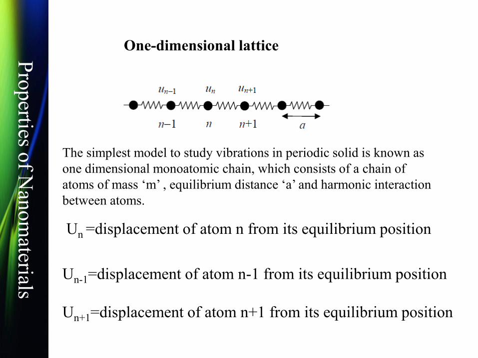
One-dimensional lattice
The simplest model to study vibrations in periodic solid is known as
one dimensional monoatomic chain, which consists of a chain of
atoms of mass ‘m’ , equilibrium distance ‘a’ and harmonic interaction
between atoms.
Un =displacement of atom n from its equilibrium position
Un-1=displacement of atom n-1 from its equilibrium position
Un+1=displacement of atom n+1 from its equilibrium position
Pro
perties o
f Nan
om
aterials
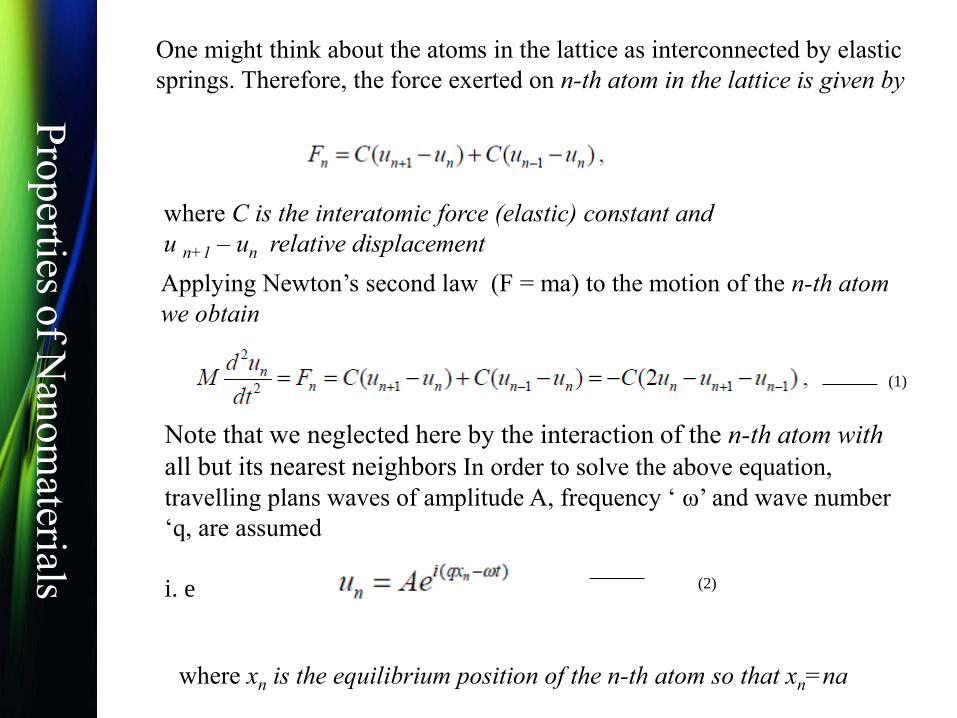
where C is the interatomic force (elastic) constant and
u n+1 – un relative displacement
One might think about the atoms in the lattice as interconnected by elastic
springs. Therefore, the force exerted on n-th atom in the lattice is given by
Applying Newton’s second law (F = ma) to the motion of the n-th atom
we obtain
Note that we neglected here by the interaction of the n-th atom with
all but its nearest neighbors In order to solve the above equation,
travelling plans waves of amplitude A, frequency ‘ ω’ and wave number
‘q, are assumed
i. e
where xn is the equilibrium position of the n-th atom so that xn=na
(1)
(2)

Pro
perties o
f Nan
om
aterials
Now substituting Eq.(2) into Eq.(1) and canceling the common
quantities (the amplitude and the
time-dependent factor)
we obtain
This equation can be further simplified by canceling the common
factor eiqna , which leads to
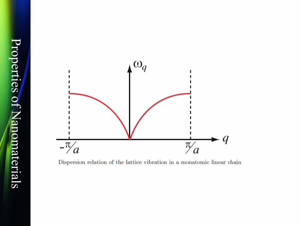
We find therefore the dispersion relation for the frequency
which is the relationship between the frequency of vibrations and
the wavevector q.
Pro
perties o
f Nan
om
aterials

Pro
perties o
f Nan
om
aterials
Diatomic 1D lattice
Now we consider a one-dimensional lattice with two non-equivalent
atoms in a unit cell
We can treat the motion of this lattice in a similar fashion as for monoatomic
lattice. However, in this case because we have two different kinds of atoms, we
should write two equations of motion:
Solution in the form of traveling mode for the two atoms leads to
Pro
perties o
f Nan
om
aterials
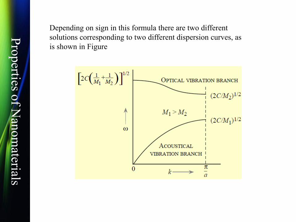
Depending on sign in this formula there are two different
solutions corresponding to two different dispersion curves, as
is shown in Figure
Pro
perties o
f Nan
om
aterials
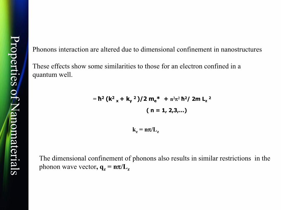
Phonons interaction are altered due to dimensional confinement in nanostructures
These effects show some similarities to those for an electron confined in a
quantum well.
= ħ2 (k2 x + ky 2 )/2 me* + n22 ħ2/ 2m Lz
2
( n = 1, 2,3,…)
kz = n/Lz
The dimensional confinement of phonons also results in similar restrictions in the
phonon wave vector, qz = n/Lz
Pro
perties o
f Nan
om
aterials
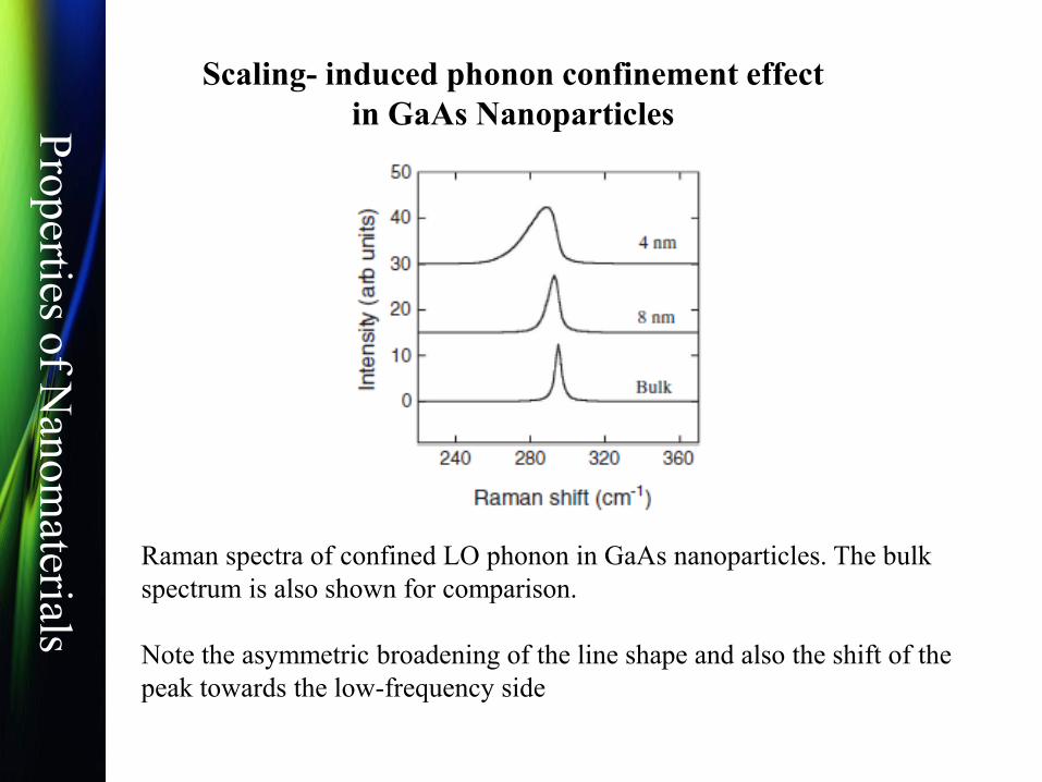
Raman spectra of confined LO phonon in GaAs nanoparticles. The bulk
spectrum is also shown for comparison.
Note the asymmetric broadening of the line shape and also the shift of the
peak towards the low-frequency side
Scaling- induced phonon confinement effect
in GaAs Nanoparticles
Pro
perties o
f Nan
om
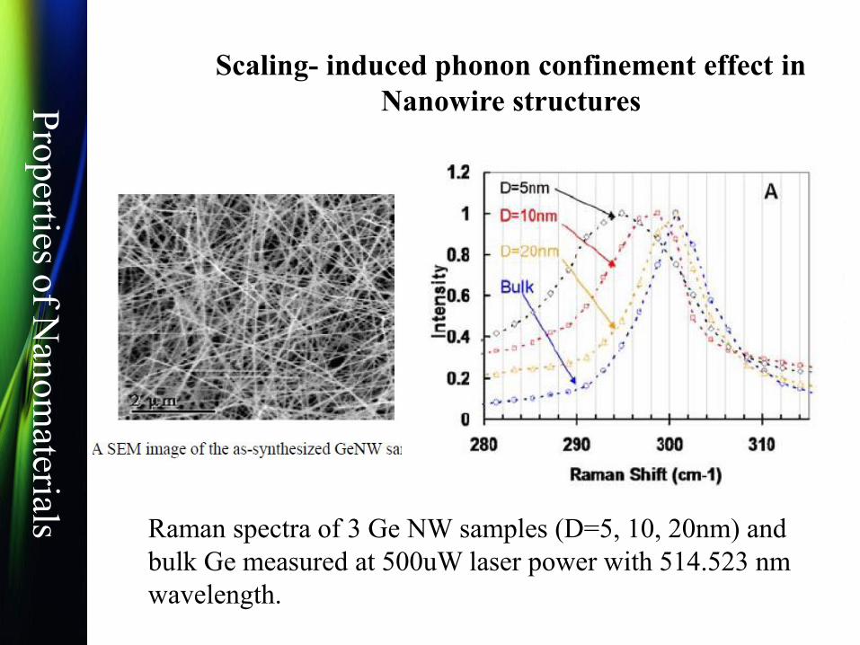
aterials Raman spectra of 3 Ge NW samples (D=5, 10, 20nm) and
bulk Ge measured at 500uW laser power with 514.523 nm
wavelength.
Scaling- induced phonon confinement effect in
Nanowire structures

Pro
perties o
f Nan
om
aterials Experimental Raman spectra four Si nanowire samples (each is a different
ensemble of Si nanowires with a different core diameter distribution, as
measured by TEM)
Pro
perties o
f Nan
om
aterials
Raman spectra develop marked asymmetry towards the low frequency
side and exhibit marginal shift in the peak position also towards the same side.
As the optical phonon dispersion curves in most solids have negative dispersion,
That is, phonon frequency decreases as a function of wavenumber, the increased
intensity in the wing of the Raman spectra on the low-frequency side basically arises
from the contribution from the phonon branch away from the zone center
Raman red shift is the consequence of the combination of the effects of size-
induced phonon confinement and surface relaxation. The structural defects
may also contribute to the Raman red shifts

Pro
perties o
f Nan
om
aterials
The dependence of the peak shift and the line
broadening on the particle size is shown in
Figure for the longitudinal optic phonon in
GaAs.
Both peak shift and the line width increase as the
particle size reduces.
However, the changes are marginal if the particle
size is larger than 10 nm.
Pro
perties o
f Nan
om
aterials
Other methods of observing the dispersion
relation of lattice vibrations
•Neutron Inelastic Scattering
•Electron Energy Loss Spectroscopy (EELS)
•Inelastic Atom Scattering