nanoskiving: a new method to produce arrays of ... · nanoskiving: a new method to produce arrays...
TRANSCRIPT
Subscriber access provided by HARVARD UNIV
Accounts of Chemical Research is published by the American Chemical Society.1155 Sixteenth Street N.W., Washington, DC 20036
Article
Nanoskiving: A New Method To Produce Arrays of NanostructuresQiaobing Xu, Robert M. Rioux, Michael D. Dickey, and George M. Whitesides
Acc. Chem. Res., 2008, 41 (12), 1566-1577• DOI: 10.1021/ar700194y • Publication Date (Web): 23 July 2008
Downloaded from http://pubs.acs.org on April 20, 2009
More About This Article
Additional resources and features associated with this article are available within the HTML version:
• Supporting Information• Access to high resolution figures• Links to articles and content related to this article• Copyright permission to reproduce figures and/or text from this article

Nanoskiving: A New Method To Produce Arraysof Nanostructures
QIAOBING XU, ROBERT M. RIOUX, MICHAEL D. DICKEY, ANDGEORGE M. WHITESIDES*
Department of Chemistry and Chemical Biology, Harvard University, 12 OxfordSt., Cambridge, Massachusetts 02138
RECEIVED ON SEPTEMBER 1, 2007
C O N S P E C T U S
This Account reviews nanoskiving-a new technique that combines thin-film deposition of metal on a topographically contoured substrate with
sectioning using an ultramicrotome-as a method of fabricating nanostruc-tures that could replace conventional top-down techniques in selected appli-cations. Photolithography and scanning beam lithography, conventional top-down techniques to generate nanoscale structures and nanostructuredmaterials, are useful, versatile, and highly developed, but they also have lim-itations: high capital and operating costs, limited availability of the facili-ties required to use them, an inability to fabricate structures on nonplanarsurfaces, and restrictions on certain classes of materials. Nanoscience andnanotechnology would benefit from new, low-cost techniques to fabricateelectrically and optically functional structures with dimensions of tens ofnanometers, even if (or perhaps especially if) these techniques have a dif-ferent range of application than does photolithography or scanning beamlithography.
Nanoskiving provides a simple and convenient procedure to producearrays of structures with cross-sectional dimensions in the 30-nm regime. Thedimensions of the structures are determined by (i) the thickness of the depos-ited thin film (tens of nanometers), (ii) the topography (submicrometer, usingsoft lithography) of the surface onto which the thin film is deposited, and (iii)the thickness of the section cut by the microtome (g30 nm by ultramicro-tomy). The ability to control the dimensions of nanostructures, combined with the ability to manipulate and position them,enables the fabrication of nanostructures with geometries that are difficult to prepare by other methods. The nanostruc-tures produced by nanoskiving are embedded in a thin epoxy matrix. These epoxy slabs, although fragile, have sufficientmechanical strength to be manipulated and positioned; this mechanical integrity allows the nanostructures to be stackedin layers, draped over curved surfaces, and suspended across gaps, while retaining the in-plane geometry of the nano-structures embedded in the epoxy. After removal of the polymer matrix by plasma oxidation, these structures generate sus-pended and draped nanostructures and nanostructures on curved surfaces. Two classes of applications, in optics and inelectronics, demonstrate the utility of nanostructures fabricated by nanoskiving.
This technique will be of primary interest to researchers who wish to generate simple nanostructures, singly or in arrays,more simply and quickly than can be accomplished in the clean-room. It is easily accessible to those not trained in top-down procedures for fabrication and those with limited or no access to the equipment and facilities needed for photoli-thography or scanning-beam fabrication.
This Account discusses a new fabrication method (nanoskiving) that produces arrays of metal nanostructures. Thedefining process in nanoskiving is cutting slabs from a polymeric matrix containing embedded, more extended metalstructures.
1566 ACCOUNTS OF CHEMICAL RESEARCH 1566-1577 December 2008 Vol. 41, No. 12 Published on the Web 07/23/2008 www.pubs.acs.org/acr10.1021/ar700194y CCC: $40.75 © 2008 American Chemical Society

What is Nanoskiving?“Nanoskiving” is the name we have given to a technique for
the fabrication of nanostructures that combines the deposi-
tion of thin films on flat or topographically patterned poly-
meric substrate using physical vapor methods with sectioning
using an ultramicrotome.1 Figure 1 outlines the procedure
used to fabricate nanomaterials by nanoskiving. The first step
utilizes an epoxy substrate obtained by curing an epoxy pre-
polymer (e.g., Araldite 502) against a flat or topographically
patterned poly(dimethylsiloxane) (PDMS) stamp formed by soft
lithography.2 A number of deposition techniques make it pos-
sible to form films with nanometer thickness on the surface of
this flat or topographically patterned epoxy. We embed the
resulting structure in more epoxy and generate an epoxy
block containing an embedded thin film. An ultramicrotome
sections this block to produce slabs that are, remarkably, as
thin as ∼30 nm. After sectioning, the slabs typically float on
the surface of water filling the sample-collecting reservoir of
the microtome. The epoxy sections can be transferred onto a
solid substrate, where the removal of epoxy by oxygen
plasma generates freestanding nanostructures; the dimensions
of the structures (Figure 1) are determined by the topogra-
phy of the substrate (x), the thickness of the deposited film
(y), and the thickness of the epoxy slab generated by sec-
tioning (z).
Figure 2 is a collage of images of both simple and com-
plex metal nanostructures fabricated by nanoskiving;3–5 these
images establish both the versatility of this technique and the
positioning of these structures on unconventional substrates.
This Review focuses on the development and use of
nanoskiving as a technique to produce nanomaterials, includ-
ing a historical context, applications, advantages, and
disadvantages.
Motivation of NanoskivingNanoskiving is fundamentally a technique that generates
structures with nanometer-scale dimensions by sectioning thin
films deposited on a master structure fabricated in epoxy. It
takes advantage of two techniques, deposition of the thin film
on the master from the vapor phase (e.g., by e-beam evapo-
ration or sputtering) and sectioning using a microtome, to pro-
duce nanometer-scale features in two dimensions. The third
dimension is fixed by the topography of the master. The mas-
ter can be prepared using conventional photolithography
(which may require a clean-room for features smaller than
∼0.5–1 µm but can be conducted outside a clean-room for
larger features). Masters are also readily available at either low
or no cost from commercial vendors or university-based
foundaries.6 Structures such as anodized aluminum mem-
branes, electron microscope grids, and patterns for optical
metrology are readily available commercially and can serve as
masters for soft lithography (see Supporting Information, Fig-
ure S1). Some structures (e.g., straight, extended wires) require
only flat surfaces. Thus, although for users with access to
clean-room facilities it may be convenient to make certain cus-
tom masters using these facilities, there are numerous ways
of obtaining appropriate masters that do not require access to
a clean-room at all.
Nanoskiving uses an ultramicrotome to produce nanostruc-
tures embedded in sub-100 nm thick slabs of supporting
matrix. We utilize this capability to produce nanostructures
with compositions and geometries that are challenging to
make using conventional techniques (e.g., extreme UV (EUV)
or X-ray photolithography, e-beam lithography (EBL), focused
FIGURE 1. Fabrication of metal nanowires by nanoskiving. Thisprocedure begins with the replication of a flat or topographicallypatterned PDMS surface in epoxy, followed by the deposition of athin film of metal on the epoxy by e-beam evaporation orsputtering. The topography of the original template determines thedimension along the x-direction. The thickness of the evaporatedmetal film determines the dimension in the y-direction and can beas small as 20 nm for gold. After embedding the thin metallic filmin more epoxy and curing, sectioning with an ultramicrotomeproduces sections with a thickness (z) as small as 50 nm using astandard 45° diamond knife. After sectioning, transfer of the epoxysection to a silicon substrate and removal of the epoxy with anoxygen plasma leaves free-standing metal nanostructures. The y-and z-dimensions of these nanostructures throughout the paper areas defined in the figure.
Nanoskiving Xu et al.
Vol. 41, No. 12 December 2008 1566-1577 ACCOUNTS OF CHEMICAL RESEARCH 1567

ion-beam (FIB)).7–9 Ultramicrotomes are generally much more
accessible and less expensive than clean-rooms, e-beam writ-
ers, and related equipment. Furthermore, many materials
(especially organics that are amenable to nanoskiving) are for-
FIGURE 2. (A) SEM image of 100-nm wide, 1-µm high step-shaped nanostructures fabricated by nanoskiving a metal-coated epoxy substrateprepatterned with 1-µm wide lines with 1-µm spacing.3 (B) SEM image of parallel gold nanowires with 20-nm spacing, by nanoskiving a flatepoxy substrate coated with a multilayer, composite Au/SiO2 film, followed by complete etching of the SiO2 spacing layers using reactive ionetching.3 (C) Dark-field optical microscopy image of “L-shaped” nanostructures patterned over a ∼3-mm2 area by nanoskiving in a directionparallel to the patterned substrate.4 (D) SEM image of double loop-shaped gold nanostructures.5 (E) SEM image of loop-shaped SiO2
nanostructures on a SiO2/Si(100) substrate by using gold loop-shaped nanostructures as a physical mask during reactive ion etching withCF4. (F) SEM image of an array of “U-shaped” gold nanostructures positioned on the curved surface of a glass rod.3 (G) SEM image of parallelgold nanowires draped over 20-µm wide “truncated-V”-shaped trenches, etched in a Si(100) surface.3 (H) Cross-bar nanostructures fabricatedby the orthogonal stacking of two epoxy slabs containing arrays of gold nanowires on top of each other. The insets are high-magnificationSEM images of the nanostructures.
Nanoskiving Xu et al.
1568 ACCOUNTS OF CHEMICAL RESEARCH 1566-1577 December 2008 Vol. 41, No. 12
bidden in semiconductor facilities. The slabs produced by
nanoskiving enable the structures to be manipulated and posi-
tioned on arbitrary substrates, including curved surfaces and
over gaps, and while retaining the relative in-plane positions
of arrays of structures.
Nanoskiving: Description of the ProcedureUltramicrotomy, which enables the reproducible generation of
sections with a thickness of <100 nm, allows biologists to
examine details of cellular or tissue ultrastructure.10 Materi-
als scientists adapted ultramicrotomy to study the details of
nanometer-thick (10–100 nm) sections of inorganic and
organic materials.11 In nanoskiving, the “sample block”, which
is ultimately sectioned by the ultramicrotome to produce
nanomaterials, is typically fabricated by embedding one or
multiple structures (e.g., a film on a flat surface or a confor-
mal film over a topologically patterned surface) within an
embedding matrix; this embedding matrix, in our work a
cross-linked epoxy resin, sections well because of its mechan-
ical properties.
Embedding Matrices: Selection of Materials. The
mechanical properties of the embedding material must be
appropriate for microtome sectioning at room temperature:
this material must have a relatively large elastic (Young’s)
modulus (E >1500 MPa).12 Materials with a value of Young’s
modulus of this magnitude are considered “brittle” and include
such common polymers as poly(methylmethacrylate) (3100
MPa), polystyrene (3050 MPa), polycarbonate (3000 MPa),
and epoxy-based resins such as Epon (3030 MPa) and Dur-
cupan (3000 MPa).12 Softer resins (E < 1500 MPa) including
materials such as low-density polyethylene (230 MPa) and
PDMS (0.5 MPa) do not allow cutting of thin sections at room
temperature, although they may when colder.
The embedding material must have some flexibility
because the sections bend at an angle of ∼90° as they move
from the sample block to the surface of the water in the
trough used for collecting the samples.12 The embedding
material must provide support for the nanostructures formed
upon sectioning in order for the structures to be manipulated.
The embedding matrix must be removed easily and quickly
by etching if desired. The adhesion of the embedding matrix
to the surface of the embedded material must be sufficient to
prevent delamination during sectioning.
Choices of Materials for Thin-Film Formation. There
are a number of methods for the deposition of thin films of
metals with nanometer accuracy; for metals, these include
physical vapor deposition, chemical vapor deposition, and
atomic layer deposition.13 The best method to form thin films
of organic materials, including conducting and electroactive
polymers, is spin-coating.
The mechanical properties of the embedded material influ-
ence the outcome of the final structures that result from sec-
tioning. Structures of malleable materials (e.g., gold and silver)
can be cut without significant catastrophic damage to the
nanostructures. Brittle materials, such as chromium and sili-
con, usually crack or break during sectioning. This limitation
can be mitigated by using an ultrasonic knife or a diamond
knife with a small wedge angle (35°) and by proper selection
of the embedding matrix.14
Knife Options. Knives are commonly made either from
glass or from high-quality, natural diamond. The formation of
high-quality sections requires the use of diamond knives
whose sharp edge has a radius of curvature of 3–6 nm.15
These knives are considerably more expensive than glass
knives. (Diamond knives range from $1700–3500, depend-
ing on the knife angle and the width of the cutting edge; the
cost of disposable glass knives is ∼$0.50/knife) Glass knives
are used typically one time because these knives dull quickly.
Diamond knives have significantly longer service life than
glass knives; they require resharpening only every 1–2 years.
The cost of resharpening ranges from $800–2200, depend-
ing on the knife specifications (knife angle and the width of
the cutting edge), and the resharpening process takes 2–3
weeks.16 In some cases, knives may dull very quickly if they
are not suited for the material to be sectioned. For example,
we found that sectioning gold thin films embedded in Araldite
epoxy with a diamond knife with a wedge angle of 25°
resulted in rapid damage of the knife edge.
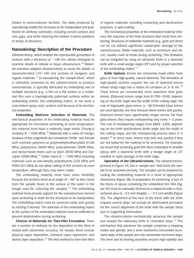
Operation of the Ultramicrotome. The ultramicrotome,
pictured in Figure 3A, has a “sample arm” that holds the sam-
ple to be sectioned securely. The samples can be prepared by
casting the embedding material in a mold of appropriate
dimensions (Figure 3B). In preparation for sectioning, a face of
the block of epoxy containing the embedded thin film (Fig-
ure 3C) must be manually trimmed to a trapezoid with a cross-
sectional area of ∼0.5 mm (height) × ∼0.5 mm (width) (Figure
3D). The alignment of the face of the block with the knife
requires several steps; we include an abbreviated procedure
for the correct alignment of the knife with the sample block
face in Supporting Information.
The ultramicrotome mechanically advances the sample
arm toward the stationary knife in controlled steps.17 The
mechanism that advances the sample comprises a stepping
motor and spindle, and a lever transforms micrometer-incre-
ment steps of the sample arm into nanometer-increment steps.
The lever and its bearing assembly ensures high stability and
Nanoskiving Xu et al.
Vol. 41, No. 12 December 2008 1566-1577 ACCOUNTS OF CHEMICAL RESEARCH 1569

FIGURE 3. (A) Photograph of an ultramicrotome and close-up photograph of the sample and diamond knife mount. (B) Photograph of theflat-embedding mold in which the Au-coated epoxy film (planar or patterned) is placed. (C) After curing, the epoxy blocks are pressed out ofthe mold. (D) A photograph of the face of the sample block trimmed with a razor blade into the shape of a trapezoid. The surface createdwith the razor blade is smoothed using a glass knife before final sectioning with a diamond knife. (E, F) Schematic illustration of the twomethods used for the collection of slabs after microtoming and for the further manipulation of these sections (e.g., positioning on asubstrate). Epoxy sections floating on the surface of water are collected either with a loop which supports a thin film of water and holds thesample by capillarity or by the “direct-capture” of the epoxy film onto a substrate (piece of silicon wafer shown in Figure 3F). (G) Bright-fieldoptical microscopy image of self-assembled multiple sections on the surface of a SiO2/Si(100) substrate.
Nanoskiving Xu et al.
1570 ACCOUNTS OF CHEMICAL RESEARCH 1566-1577 December 2008 Vol. 41, No. 12

step increments as small as approximately 1 nm. After each
incremental advance of the sample, the sample arm moves
through a down stroke (total displacement ∼1 cm) and then
returns to its starting position before advancing again. Dur-
ing the downstroke of the sample arm, the sample is forced
against the edge of the knife to section the sample. The sec-
tions are generated at rate of 1 Hz; this rate allows for the pro-
duction of 200 slabs in 10 min.
It is not entirely clear how the microtome produces nanom-
eter-thick sections. There are two mechanisms postulated for
sectioning:12 (i) During direct-sectioning (or “true-sectioning”),
the edge of the knife remains in contact with the epoxy block
through the entire process of section removal. This mecha-
nism is believed to be the primary mechanism for soft, plas-
tic materials. (ii) In cleavage-fracture, the edge of the knife
initiates a crack that propagates in the sample block. This
mechanism is believed to be responsible for sectioning hard,
brittle materials. Both mechanisms could operate during the
sectioning of heterogeneous materials (e.g., heterostructures
and interfacial materials).
Collecting and Transferring the Sections. “Wet section-
ing” is the most commonly used sectioning technique because
of its convenience; the sections float onto the surface of water
(which fills the trough on the back side of the knife) as they
come off of the edge of the knife. The water reduces dam-
age (e.g., compression) to the sample by reducing the friction
between the back edge of the knife and the epoxy section.
The sections (i.e., the epoxy slabs with embedded metal nano-
structures) floating in the trough can be collected and trans-
ferred by several techniques to solid substrates. The slabs can
be removed from the trough using a collection loop (2-mm
diameter) (Figure 3E),10 in which a meniscus of water that
spans the loop supports the sample. The sample can be trans-
ferred to a substrate (e.g., silicon wafer or TEM grid) by touch-
ing the loop to the substrate (by capillary action). Alternatively,
the samples can be collected by submerging the substrate
directly below the floating epoxy section(s) and pulling the
substrate toward the section(s) in such a way that it (or they)
settle on the substrate (Figure 3F). Figure 3G is an example of
the direct deposition of a series of epoxy sections on a piece
of silicon wafer.
Removing the Embedding Matrix. After transfer of the
section to a substrate, the embedding matrix can be removed
to produce free-standing nanomaterials. To remove the
embedding matrix (Araldite 502), we expose it to an oxygen
plasma. The time necessary to remove the embedding matrix
completely is dependent upon the thickness of the section
removed with the ultramicrotome and the character of the
plasma (i.e., oxygen partial pressure, power, and time).
Fabrication of Complex NanostructuresUsing Topographically PatternedSubstratesFigure 1 illustrates the simplest possible application of nanosk-
iving: sectioning a flat epoxy substrate coated with a thin film
of metal to produce wires. We are able to fabricate more com-
plex nanostructures by choosing the topography of the sub-
strate and by rationally selecting the orientation used to
section the substrate (Figure 4A). Figure 4B shows a free-stand-
ing, step-shaped nanostructure fabricated by nanoskiving
epoxy replicas of photolithographically patterned 1-µm wide
lines with 1-µm separation in a direction perpendicular to the
plane of the patterned substrate.4 One advantage of perpen-
dicular sectioning is that a single block can be sectioned to
form multiple samples, (e.g., a 2-D metal film embedded in an
epoxy matrix (1-cm long) can generate ∼105 sections with
50-nm thickness); nanoskiving is, thus, in principle, a
“nanomanufacturing” process.
Figure 4C shows an array of gold nanowires fabricated by
sectioning epoxy replicas in the plane parallel to the patterned
substrate.5 Photolithography (or another type of patterning
method) defines one dimension; this dimension thus can be
varied and controlled within the limits of the patterning tech-
nique. Parallel-sectioning generates large arrays of metallic
nanostructures in a single section. The number of elements
defined in the patterning step determines the number of nano-
structures in the section. A shortcoming of the parallel-sec-
tioning approach in some applications is that only a limited
number of individual sections can be generated from a sin-
gle sample because of the limited aspect ratio (height:width)
of features fabricated by photolithography. For example, a cir-
cular post with a 2-µm diameter and 2-µm height defined by
photolithography can generate a maximum of approximately
forty 50-nm thick sections when sectioned in the plane where
the top of the circle resides. This limitation, however, could be
overcome through the use of a high-aspect-ratio fabrication
technique,18,19 such as LIGA, deep RIE, and surface micro-
machining.
Applications of Nanostructures and Arraysof Nanostructures Fabricated byNanoskivingThe following examples demonstrate the utility of nano-
skiving:
Nanoskiving Xu et al.
Vol. 41, No. 12 December 2008 1566-1577 ACCOUNTS OF CHEMICAL RESEARCH 1571

Frequency-Selective Surface-Plasmonic Nanowires.Localized surface plasmon resonance occurs when incident
light resonates with the collective excitation of the conduc-
tion electrons on the surface of metallic nanostructures.20
Local electromagnetic fields near the structure can be many
orders of magnitude higher than the incident fields; these
strong, oscillating fields generate intense scattered light
around the wavelength of the resonant peak. The enhance-
ment in local field and strong scattering is useful for a num-
ber of applications, including surface-enhanced Raman
scattering,21 subwavelength optical waveguides,22 biolabel-
ing, and biosensing.23 The magnitude, peak wavelength, and
spectral bandwidth of the plasmon resonance of a nanostruc-
ture depend on the size, shape, material of fabrication, and
local environment (i.e., dielectric properties) of the particle.24
Nanoskiving provides a simple route to uniform metallic
nanowires of well-defined cross-sectional dimensions.
Figure 5A and B show color, dark-field optical images (and
corresponding scattering spectra at visible wavelengths) of a
series of gold nanowires with the same dimensions in length
(x ) 2 µm) and width (y ) 20 nm), but different in height (the
z-dimension ranges from 30 to 100 nm), which is the thickness
of the epoxy sections formed by nanoskiving. The resonant
wavelength of the surface plasmons on gold nanowires depends
on the aspect ratio of the cross-section of the nanowires. The
spectrum shifts to longer wavelength as the aspect ratio (z/y) of
the cross-section of the nanowire increases. A similar shift in the
resonant wavelength of the surface plasmons is observed when
the aspect ratio of the cross-section of the nanowire increases on
changing the thickness of the evaporated metal film (y) while
holding the thickness (z) of the section constant.25
Nanostructures as Templates for the Fabrication ofan Array of Nanoslits. Nanoskiving has the ability to gener-
ate certain types of “master” structures; that is, it does not
FIGURE 4. (A) Schematic illustration of the procedure used to fabricate complex nanostructures by sectioning a topographicallypatterned substrate (1-µm lines with 1-µm separation) positioned in different orientations (relative to edge of the knife). (B, C) Thedifference in the shape of the nanostructures obtained from the same sample with different orientation of the sample and knife: (B)perpendicular-sectioning to the substrate patterned with rectangular ridges leads to the formation of continuous stepped structures and(C) parallel-sectioning leads to parallel 1-µm lines with 1-µm separation. Both (B) and (C) are SEM images of gold nanostructuressupported on a SiO2/Si(100) substrate.
Nanoskiving Xu et al.
1572 ACCOUNTS OF CHEMICAL RESEARCH 1566-1577 December 2008 Vol. 41, No. 12

require the nanostructures to be written in a separate step
using a technique such as e-beam writing or FIB.8 We dem-
onstrated the fabrication of large-area arrays (∼mm2) of nano-
structures by sectioning in a plane parallel to the patterned
substrate containing structures with different shapes (e.g.,
closed-loop and open nanostructures), defined by photolithog-
raphy and selective metal deposition using shadow evapora-
tion.4 We are able to transfer these arrays of nanostructures
into PDMS and other polymers by soft lithography.2 The nano-
structures from nanoskiving can be the physical master for the
transfer of the nanostructures into other materials, such as a
layer of SiO2, through reactive ion etching (Figure 2E).
Arrays of nanostructures can also be used as shadow
masks to generate an inverse replica of the structures onto the
substrate (e.g., a gold film). Figure 6A shows the arrays of
square-loop-shaped gold nanostructures (50-nm wide and
150-nm tall) fabricated by nanoskiving4,5 and subsequently
coated with a 5-nm thick Ti adhesion layer, followed by a
50-nm thick Au film, both by electron beam evaporation. The
adhesion between the substrate and the loop-shaped nano-
structures is much poorer than the adhesion between the
substrate and the titanium adhesion layer of the additional
evaporated gold film. The loop-shaped nanostructures on
the substrate can be removed using adhesive tape or soni-
cation to generate roughly loop-shaped nanoslits in a Au/Ti
film (Figure 6B).
Fabrication of Addressable Nanoelectrode Embeddedin a Polymer Matrix. One of the challenges for nanoscience
is fanout, making connections between the nanostructures and
external electrical circuits.26 The most common technique to
connect nanowires to electrical circuits uses a combination of
e-beam lithography and photolithography;27 nanoscience
would benefit from new techniques.8,28–30
We have used nanoskiving to fabricate an array of nano-
electrodes that can be addressed from the back face of the
slab of epoxy resin. We deposited a 50-nm thick gold film by
electron-beam evaporation on an epoxy substrate patterned
with parallel lines. The collimated metal deposition prevents
metal coating on the sidewall of the line. We embedded the
resulting structure in more epoxy, generating an epoxy block
containing isolated metal wires. We exposed the cross-sec-
tion of the block by cutting the sample perpendicular to the
plane of the metal wire using an ultramicrotome at –120°C.31
The low-temperature sectioning minimizes the delamination
between the polymer and metal film. Sectioning of the sam-
ple block exposes a cross-section of the embedded metal
FIGURE 5. Surface plasmon resonance of gold nanowires withdifferent cross-sectional dimensions. (A) Dark-field opticalmicroscopy images of 2-µm (x) long gold nanowires with differentcross-sectional dimensions. The dimensions of the cross-section arethe thickness of the gold film (y) and the thickness of the epoxysection (z) (respectively). (B) The scattering spectra in the visibleregime of the gold nanowires with the dimensions correspondingto the gold nanowires in (A). As the aspect ratio (z/y) of the cross-section of the nanowire increases, the resonance of the surfaceplasmons shifts to higher energy.
FIGURE 6. (A) SEM image of an array of gold nanorings on a SiO2/Si(100) substrate. (B) SEM image of the same surface after coatingthe substrate with an adhesion layer (5 nm Ti) and a 50-nm thickAu layer, and removal of the original gold nanorings by sonication,generating inverse replicas of the gold nanorings in the thin-film ofgold.
Nanoskiving Xu et al.
Vol. 41, No. 12 December 2008 1566-1577 ACCOUNTS OF CHEMICAL RESEARCH 1573

wires. The thickness of the metal film (50 nm) determines the
width of the exposed metal. The exposed metal has the use-
ful feature that it can be addressed electrically on the side of
the polymer slab opposite the exposed metal edges (Figure
7A). The electrodeposition of more gold on the metal edge
exposed at the surface of the epoxy slab (Figure 7B) demon-
strated the electrical conductivity of the embedded nanostruc-
tures (Figure 7C). This method thus provides a route to a kind
of addressable nanoelectrodes that cannot be easily
achieved with conventional nanofabrication techniques
(which put connections in the plane of the electrodes). This
fabrication technique does not circumvent the common
problem of addressing each electrode individually; in fact,
this was not the intention of this demonstration. We believe
that a current approach in our laboratory based on shadow
deposition and nanoskiving may enable individually
addressable electrodes.
Stacking Multilayer Structures to Make Functional
Quasi-3D Materials. These thin polymer slabs containing the
embedded nanostructures have sufficient mechanical strength
to be manipulated to fabricate certain types of arrays of nano-
structures that are otherwise difficult to prepare. For exam-
ple, we positioned (by hand) nanometer-sized features by
manipulating the epoxy sections (∼1 mm2) onto curved sur-
faces (Figure 2D) and across gaps (Figure 2E).3 Stacking the
epoxy films on top of each other formed quasi-3D nanostruc-
tures (e.g., cross-bar nanostructures in Figure 2F).
Figure 8A outlines a procedure to construct multilayer
structures for applications in frequency-selective surfaces at
mid-IR wavelengths by stacking sections on top of each oth-
er.3 The bottom layer of epoxy contained an array of
U-shaped gold nanostructures, with dimensions 50 nm (y) ×100 nm (z). We stacked a second section of epoxy (200-nm
thick with no embedded nanostructures) on top of the epoxy
slab containing the U-shaped nanostructures, followed by a
third layer containing parallel gold nanowires with dimenions
50 nm (y) × 100 nm (z) on top of the stack (Figure 8B).
These large-area, highly ordered arrays of nanostructures
have the right dimensions required to test many of the prop-
erties of nanostructures acting as true plasmonic oscillators in
the IR regions of the electromagnetic spectrum. We demon-
strated the ability of single layers of arrays of square loop and
open (L- and U-shaped) nanostructures to serve as mid-infra-
red band-stop optical filters.4 Figure 8C shows the transmis-
sion spectra of the stacked multilayer nanostructures and the
individual films of epoxy-embedded nanostructures. The
mid-IR transmission spectrum had three resonant peaks (5.1,
6.5, and 14.5 µm) for the array of U-shaped nanostructures;
we attribute these resonances to first-order and harmonic res-
onant plasmon modes induced by the unpolarized incident
infrared light.4 The transmission spectrum of a single epoxy
slab (100-nm thick) containing periodic parallel lines had no
resonant peaks, and the transmission decreased continuously
in the 4- to 16-µm region. The transmission spectrum of the
stacked multilayer assembly has a significantly more asym-
metric line shape than the transmission spectra of the array of
U-shaped nanostructures, with a single resonant peak at ∼7
µm, which is red-shifted from the 6.5-µm peak observed with
the U-shaped nanostructures. The slab containing arrays of
nanowires acts as a mid-IR wire grid polarizer3 and attenu-
ates the two resonant peaks excited by the incident p-polar-
ized light from arrays of U-shaped nanostructures.4
FIGURE 7. (A) Schematic illustration of the experimental setup usedto demonstrate the electrical connectivity of the exposed edge ofgold wires embedded in an epoxy matrix. Electrodeposition of goldonto the exposed gold edge of embedded wires was accomplishedby connecting a wire to one face of the slab with InGaSn solderand conductive carbon tape. The electrodeposition of gold occurson the opposite exposed face. (B) The SEM image of the embedded50-nm wide gold film within a continuous epoxy matrix. (C) Theexposed metal edge (opposite to the electrical connection) is thecathode for the electrodeposition of additional gold onto theconductive exposed edge of the nanwires embedded in theinsulating matrix. Some edges are not conductive; evidenced by thelack of gold deposition during electrodeposition.
Nanoskiving Xu et al.
1574 ACCOUNTS OF CHEMICAL RESEARCH 1566-1577 December 2008 Vol. 41, No. 12

Comparison with Other TechniquesNanoskiving is a simple and inexpensive route for the
production of nanomaterials (ranging from simple, single
nanostructures to large-area arrays of more complex nano-
structures) with minimal facilities. There are examples of
nanostructures (Figures 2A,C-H, and 4–8) in which we used
clean-room facilities to fabricate the template (defines x-di-
mension), but the nanoscale features come from a combina-
tion of evaporation/deposition and sectioning with the
ultramicrotome, not from photolithography. The smallest x-di-
mension demonstrated in this Review is 1–2 µm and does not
necessarily require a clean-room for its fabrication, just access
to a contact aligner. The fabrication of the array of parallel
nanowires (Figure 2B) required no access to a clean-room. We
demonstrated in a previous publication that commonly avail-
able masters (i.e., diffraction grating) can be used to fabricate
nanostructures without the need of a clean-room.3
Nanoskiving can generate patterns of nanostructures with
relatively large areas (∼mm2) (Figure 4). Self-assembly of the
epoxy sections containing the nanostructures (Figure 3G)
allows tiling of patterned arrays of nanostructures over areas
of cm2; this area of patterning is still not comparable with the
areas (∼500 cm2) of patterning achieved with photolithogra-
phy and nanoimprint lithography.32 Nanostructures with high-
aspect-ratio structures that are difficult or impossible to
fabricate by other methods can be generated easily with
nanoskiving (Figure 2A). Nanoskiving allows for the position-
ing and assembly of nanomaterials because the slices can be
physically manipulated. The slices can be positioned over non-
planar topologies including curved surfaces and gaps or
stacked on another slab of epoxy containing embedded nano-
structures to form multilayer, quasi-3D structures (Figure
2D-F).
Nanoskiving substitutes “sectioning by microtome” for the
“exposure” in photolithography, “writing” in e-beam lithogra-
phy and scanning probe lithography, and “printing/molding”
in soft and imprint lithography. Nanoskiving can serve as a
method for both mastering and replicating arrays of nano-
structures. In the role of a mastering technology, it is related,
albeit distantly, to electron-beam or scanning probe lithogra-
phy; in the role of a replicating technology, it has some anal-
ogy to photolithography or soft lithography. The versatility of
FIGURE 8. (A) Schematic illustration of the procedure for constructing multilayer structures by the stacking of multiple sections. (B) SEMimage of the stacked, epoxy-embedded multilayer structure. The inset is a high-magnification SEM image of the stacked structure. (C) Mid-IRtransmission spectra of the individual elements and multilayer structure embedded in epoxy.
Nanoskiving Xu et al.
Vol. 41, No. 12 December 2008 1566-1577 ACCOUNTS OF CHEMICAL RESEARCH 1575

nanoskiving as a technique for both mastering and replicat-
ing is not found in any of the other methods used for
nanofabrication.
Nanoskiving also has, of course, limitations. Nanoskiving is
currently restricted to generating unconnected line structures.
The inability to fabricate connected structures limits the appli-
cation of these nanostructures in applications such as mak-
ing integrated circuits. It also does not currently have the
stability in the pattern necessary to generate sections that can
be registered precisely.
OutlookPotential Applications of Nanoskiving. Nanoskiving is not
competitive with photolithography or scanning beam meth-
ods for making the multilayer, registered structures required
for integrated circuits. Instead, this technique will be of pri-
mary interest to researchers who wish to generate simple
nanostructures, singly or in arrays, more simply and quickly
than can be accomplished in the clean-room. It is easily acces-
sible to those not trained in top-down procedures for fabrica-
tion and those with limited or no access to the equipment and
facilities needed for photolithography or scanning-beam
fabrication.
Challenges Associated with Nanoskiving As a Tool forResearch and Manufacturing. Many of the procedures
important in nanoskiving, especially sample mounting and
aligning, are presently done exclusively by hand, and the gen-
eration of high-quality sections requires an experienced micro-
tome user. The development of an automated microtome
instrument would be required to reduce or eliminate the influ-
ence of the user on the quality of the section. Nanoskiving
would also benefit from advances in the ultramicrotome setup,
such as (i) ease of alignment of the knife edge with the face
of the sample, (ii) ease of manipulation and positioning of thin
polymer sections, and (iii) methods for the integration of nano-
structures produced by nanoskiving into other systems, such
as optical fibers or microfabricated devices.
The sectioning procedure can lead to artifacts and defects
in the nanostructures. Brittle materials, such as SiO2, tend to
crack and form small segments during sectioning. The sam-
ple can compress during sectioning, causing deformation of
the nanostructures and also causing the true thickness of the
individual nanostructures or individual elements in the array
of nanostructures to be greater than the nominal thickness.33
The compression in the sectioning process can be minimized
with the use of ultrasonic knives14 and by the choice of an
embedding material that decreases the amount of compres-
sion.34
This research was supported by NIH (GM065364) and by
DARPA (subaward to G.M.W. from the Center for Optofluidic
Integration at the California Institute of Technology). The
research used MRSEC and NSEC facilities supported by NSF
(DMR-0213805 and PHY-0117795) and at the Center for
Nanoscale Systems (CNS: NSE ECS-0335765). R.M.R. acknowl-
edges NIH for a postdoctoral fellowship (1 F32 NS060356). Our
colleagues Federico Capasso and Jiming Bao helped with the
optical characterization. We acknowledge Dr. Reinhard Lihl of
Leica Microsystems and Dr. Helmut Gnägi of Diatome for
numerous private communications about the operation of a
microtome and technical details of knife preparation and usage.
Supporting Information Available. A collection of images of
potential masters for soft lithography that can be purchased
commercially and/or fabricated outside of a clean-room facil-
ity and the procedure for correct alignment of the microtome
is given. This information is available free of charge via the
Internet at http://pubs.acs.org.
BIOGRAPHICAL INFORMATION
Qiaobing Xu was born in 1977 in Jiangsu, China. He received hisB.S. degree in 1999 and his M.S. degree in 2002 from Jilin Uni-versity, P. R. China. In 2007 he earned is Ph.D. degree in chem-istry at Harvard University under his advisor, Professor George M.Whitesides. He is now a postdoctoral research fellow at the Mas-sachusetts Institute of Technology with Professor Robert S. Langer.His research interests include micro- and nanotechnology, mate-rials science, and bioengineering.
Robert M. Rioux was born in 1975 in Hartford, CT. He receiveda Ph.D. in physical chemistry from the University of California, Ber-keley (2006) under his advisor, Professor Gabor A. Somorjai. Heis currently a National Institute of Health postdoctoral fellow in thelaboratory of Professor George M. Whitesides at Harvard Univer-sity. His research interests include soft lithography tools for neu-robiology, unconventional nanofabrication, surface science, andheterogeneous catalysis.
Michael D. Dickey was born in 1976 in Raleigh, NC. He receivedhis B.S. in chemical engineering (1999) from the Georgia Insti-tute of Technology and a Ph.D. in chemical engineering from theUniversity of Texas (2006) under his advisor, Professor C. GrantWillson. He is currently a postdoctoral fellow in the laboratory ofProfessor George M. Whitesides at Harvard University. Hisresearch interests include unconventional nanofabrication, micro-and nanotechnology, and materials science.
George M. Whitesides was born in Louisville, KY, in 1939. Hereceived his A.B. degree from Harvard University in 1960 and hisPh.D. degree with Professor John D. Roberts from the California Insti-tute of Technology in 1964. He was a member of the faculty of theMassachusetts Institute of Technology from 1963 to 1982. Hejoined the Department of Chemistry of Harvard University in 1982,where he is now the Woodford L. and Ann A. Flowers University Pro-
Nanoskiving Xu et al.
1576 ACCOUNTS OF CHEMICAL RESEARCH 1566-1577 December 2008 Vol. 41, No. 12

fessor. His research interests include physical organic chemistry,materials science, biophysics, complexity, surface science, microflu-idics, self-assembly, micro- and nanotechnology, cell-surface bio-chemistry, and rational ligand design.
FOOTNOTES
*To whom correspondence should be addressed. Tel: (617) 495-9430. Fax: (617) 495-9857. Email: [email protected].
REFERENCES1 According to the Webster-Merriam dictionary, the verb “to skive” is of Scandinavian
origin and defined as “to cut off in thin layers or pieces”. It is often used in the context ofcutting rubber or leather. Skiving apparently also has a slang usage in parts of the UnitedKingdom in which it means “skipping an obligation” (e.g., a class).
2 Xia, Y.; Whitesides, G. M. Soft lithography. Angew. Chem., Int. Ed. 1998, 37, 550–575.
3 Xu, Q.; Rioux, R. M.; Whitesides, G. M. Fabrication of complex metallicnanostructures by nanoskiving. ACS Nano 2007, 1, 215–227.
4 Xu, Q.; Bao, J.; Rioux, R. M.; Perez-Castillejos, R.; Capasso, F.; Whitesides, G. M.Fabrication of large-area patterned nanostructures for optical applications bynanoskiving. Nano Lett. 2007, 7, 2800–2805.
5 Xu, Q.; Perez-Castillejos, R.; Li, Z. F.; Whitesides, G. M. Fabrication of high-aspect-ratio metallic nanostructures using nanoskiving. Nano Lett. 2006, 6, 2163–2165.
6 There are a number of university-based foundaries with soft lithography services.For example, the Center for Nanotechnology at the University of Washington (http://www.nnin.org/nnin_washington.html), the Center for Nanoscale Systems at HarvardUniversity (http://www.cns.fas.harvard.edu), the Stanford Microfluidics Foundry atStanford University (http://thebigone.stanford.edu/foundry/), and the KavliNanoscience Institute Microfluidic Foundry at the California Institute of Technology(http://kni.caltech.edu/foundry/) are a few examples of foundaries in the UnitedStates.
7 Gates, B. D.; Xu, Q.; Love, J. C.; Wolfe, D. B.; Whitesides, G. M. Unconventionalnanofabrication. Annu. Rev. Mater. Res. 2004, 34, 339–372.
8 Gates, B. D.; Xu, Q.; Stewart, M.; Ryan, D.; Willson, C. G.; Whitesides, G. M. Newapproaches to nanofabrication: molding, printing, and other techniques. Chem. Rev.2005, 105, 1171–1196.
9 Love, J. C.; Estroff, L. A.; Kriebel, J. K.; Nuzzo, R. G.; Whitesides, G. M. Self-assembled monolayers of thiolates on metals as a form of nanotechnology. Chem.Rev. 2005, 105, 1103–1169.
10 Glauert, A. M. Practical Methods in Electron Microscopy; American ElsevierPublishing Co. Inc.: New York, 1974.
11 Plummer, H. K. Reflections on the use of microtomy for materials science specimenpreparation. Microsc. Microanal. 1997, 3, 239–260.
12 Acetarin, J. D.; Carlemalm, E.; Kellenberger, E.; Villiger, W. Correlation of somemechanical properties of embedding resins with their behavior in microtomy. J.Electron Microsc. Tech. 1987, 6, 63–79.
13 Seshan, K. Handbook of Thin Film Deposition Techniques; William AndrewPublishing Inc.: New York, 2002.
14 Studer, D.; Gnaegi, H. Minimal compression of ultrathin sections with use of anoscillating diamond knife. J. Microsc. 2000, 197, 94–100.
15 Matzelle, T. R.; Gnaegi, H.; Ricker, A.; Reichelt, R. Characterization of the cuttingedge of glass and diamond knives for ultramicrotomy by scanning force microscopyusing cantilevers with a defined tip geometry. Part II. J. Microsc. 2003, 209, 113–117.
16 http://www.emsdiasum.com/Diatome/diamond_knives/default.htm.17 The details of operation of a microtome are proprietary. This information was kindly
provided by Dr. R. Lihl, R & D manager at Leica Microsystems.18 del Campo, A.; Greiner, C. SU-8: a photoresist for high-aspect-ratio and 3D
submicron lithography. J. Micromech. Microeng. 2007, 17, R81–R95.19 Friedrich, C. R.; Vasile, M. J. Development of the micromilling process for high-
aspect-ratio microstructures. J. Microelectromech. Syst. 1996, 5, 33–38.20 Willets, K. A.; Van Duyne, R. P. Localized surface plasmon resonance spectroscopy
and sensing. Annu. Rev. Phys. Chem. 2007, 58, 267–297.21 Kneipp, K.; Kneipp, H.; Kneipp, J. Surface-enhanced Raman scattering in local
optical fields of silver and gold nanoaggregatess - From single-molecule Ramanspectroscopy to ultrasensitive probing in live cells. Acc. Chem. Res. 2006, 39, 443–450.
22 Maier, S. A.; Atwater, H. A. Plasmonics: Localization and guiding of electromagneticenergy in metal/dielectric structures. J. Appl. Phys. 2005, 98, 011101.
23 Rosi, N. L.; Mirkin, C. A. Nanostructures in biodiagnostics. Chem. Rev. 2005, 105,1547–1562.
24 Wang, H.; Brandl, D. W.; Nordlander, P.; Halas, N. J. Plasmonic nanostructures:Artificial molecules. Acc. Chem. Res. 2007, 40, 53–62.
25 Xu, Q.; Bao, J.; Capasso, F.; Whitesides, G. M. Surface plasmon resonances of free-standing gold nanowires fabricated by nanoskiving. Angew. Chem., Int. Ed. 2006,45, 3631–3635.
26 Mendes, P. M.; Preece, J. A. Precision chemical engineering: integratingnanolithography and nanoassembly. Curr. Opin. Colloid Interface Sci. 2004, 9, 236–248.
27 Li, Y.; Qian, F.; Xiang, J.; Lieber, C. M. Nanowire electronic and optoelectronicdevices. Mater. Today 2006, 9, 18–27.
28 Ginger, D. S.; Zhang, H.; Mirkin, C. A. The evolution of dip-pen nanolithography.Angew. Chem., Int. Ed. 2004, 43, 30–35.
29 Guo, L. J. Nanoimprint lithography: Methods and material requirements. Adv. Mater.2007, 19, 495–513.
30 Menard, E.; Meitl, M. A.; Sun, Y. G.; Park, J. U.; Shir, D. J. L.; Nam, Y. S.; Jeon, S.;Rogers, J. A. Micro- and nanopatterning techniques for organic electronic andoptoelectronic systems. Chem. Rev. 2007, 107, 1117–1160.
31 Xu, Q.; Gates, B. D.; Whitesides, G. M. Fabrication of metal structures withnanometer-scale lateral dimensions by sectioning using a microtome. J. Am. Chem.Soc. 2004, 126, 1332–1333.
32 Li, N. H.; Wu, W.; Chou, S. Y. Sub-20-nm alignment in nanoimprint lithographyusing Moire fringe. Nano Lett. 2006, 6, 2626–2629.
33 Richter, K. Cutting artifacts on ultrathin cryosections of biological bulk specimens.Micron 1994, 25, 297–308.
34 Private communication with Dr. Helmut Gnägi of Diatome Ltd., Switzerland.
Nanoskiving Xu et al.
Vol. 41, No. 12 December 2008 1566-1577 ACCOUNTS OF CHEMICAL RESEARCH 1577