nanoscale molecular- switch crossbar circuits group 2 j. r. edwards pierre emelie mike logue zhuang...
TRANSCRIPT

Nanoscale molecular-switch crossbar circuitsGroup 2J. R. EdwardsPierre EmelieMike LogueZhuang Wu

Outline
Introduction and basic principles of crossbar circuits
Growth techniques Current research results Summary

Introduction
Nearly a billion transistors on a silicon chip Lengths of the smallest chip will shrink to
nearly the molecular scale Major innovations are needed to reach a
length for functional features around 10 nm (30 atoms long)

Quantum Computing A classical computer has a memory made up of bits A quantum computer maintains a set of qubits and operates by
manipulating them A qubit can hold a “1”, a “0” or a superposition of these Qubits can be implemented using the two spin states of an electron If large-scale quantum computers can be built, they will be able to
solve certain problems faster than any classical computer
It is however decades away from realization It remains unclear how useful it would be for most applications
Several groups are investigating another path (one group at the Hewlett-Packard Laboratories was the precursor)
The crossbar architecture

Crossbar Architecture
Configurable crossbar architecture
Array of crossing nanowires
Switch is formed at the junction between two crossing nanowires
Nanowires are separated by a single monolayer of molecules

Crossbar Architecture
VT=0.2 V Voltage limit |VT|<2 V The switch remains in the
state it was last set Positive (negative) cycling
voltages reversibly switch the device to the “ON” (“OFF”) state
Low resistance state
“ON” state
High resistance state
“OFF” state

Crossbar ArchitectureVT=0.2 V
Curves are offset for clarity
“OFF” state (ohmic response)
Rd=8.1x10⁶ Ω
Counter-clockwise IV hysteresis
“ON” state (ohmic response)
Rd=4.8x10⁵ ΩClockwise IV hysteresis
“OFF” state (ohmic response)
Rd=9.2x10⁶ Ω
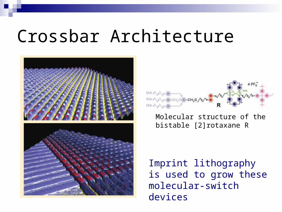
Crossbar Architecture
Molecular structure of the bistable [2]rotaxane R
Imprint lithography is used to grow these molecular-switch devices

Crossbar Architecture
How do we control these crossbars and link them with external systems in order to perform memory and/or logic functions?
By using micron-scale silicon ICs
How do we bridge the gaps in size and number of wires between nanoelectronics and the conventional-scale silicon ICs?
=> By using a demultiplexer

Demultiplexer
Demultiplexer enables conventional wires on silicon chips to control a great number of nanowires
If k is the number of conventional wires, the multiplexer can control 2k nanowires
An additional d conventional wires provide redundancy to work despite broken connections
Applications and Advantages This configurable architecture can be used to perform memory
and/or logic function The wires can be scales continuously down to molecular sizes while
the number of wires in the crossbar can be scaled up arbitrarily to form large-scale generic circuits
It requires only 2N communication wires to address 2N nanowires This allows the nano-circuit to communicate efficiently with external
circuits It can tolerate defective elements generated during the fabrication
process by introducing redundancy Fabrication is feasible and potentially inexpensive
Next: More details on the fabrication process and some results will be presented

Fabrication Overview
Pattern bottom electrode and deposit rotaxane monolayer switching material
Protective Ti layer evaporated onto film
Pattern top electrode Remove excess
Why Nanoimprint Lithography
Pattern small feature sizes High throughput Low cost Precludes damage to sensitive
components

Nanoimprint Lithography (NIL)
But at smaller feature sizes, resist adheres to mold.

Double-layer UV-curable NIL

Double-layer UV-curable resist
Highly cross-linked top imaging layer, mechanically strong
Bottom transfer layer with good liftoff, also serves to planarize the surface
Exceptional thickness uniformity
Thickness distribution of spin-coated UV-curable imprint resist over a 4 inch wafer.

Double-layer UV-curable NIL
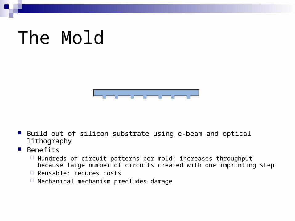
The Mold
Build out of silicon substrate using e-beam and optical lithography Benefits
Hundreds of circuit patterns per mold: increases throughput because large number of circuits created with one imprinting step
Reusable: reduces costs Mechanical mechanism precludes damage

Double-layer UV-curable NIL
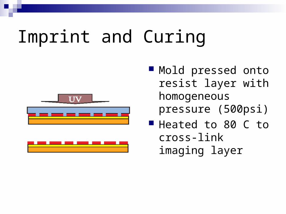
Imprint and Curing
Mold pressed onto resist layer with homogeneous pressure (500psi)
Heated to 80 C to cross-link imaging layer

Double-layer UV-curable NIL
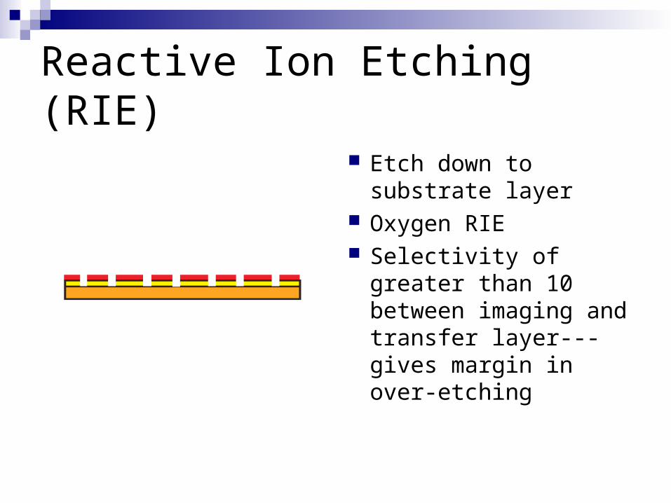
Reactive Ion Etching (RIE)
Etch down to substrate layer
Oxygen RIE Selectivity of greater
than 10 between imaging and transfer layer---gives margin in over-etching

RIE
Reactive gas and accelerated ions increase etch rate
Etch product may form passivation layer on the side wall---preventing lateral etching.
Anisotropic

Double-layer UV-curable NIL

Metal and Liftoff
Metal (Ti and Au, Pt) evaporated onto pattern
Solubility of transfer layer provides good liftoff of resist
Wetting problem

Adhesion and Wetting
Hydrophobic imaging layer reduces adhesion forces between mold and resist but also prevents solvent from getting into the feature gaps
Solution: treat the surface with O2 plasma to improve wetting property of the resist.

Nanoscale cross-bar circuits
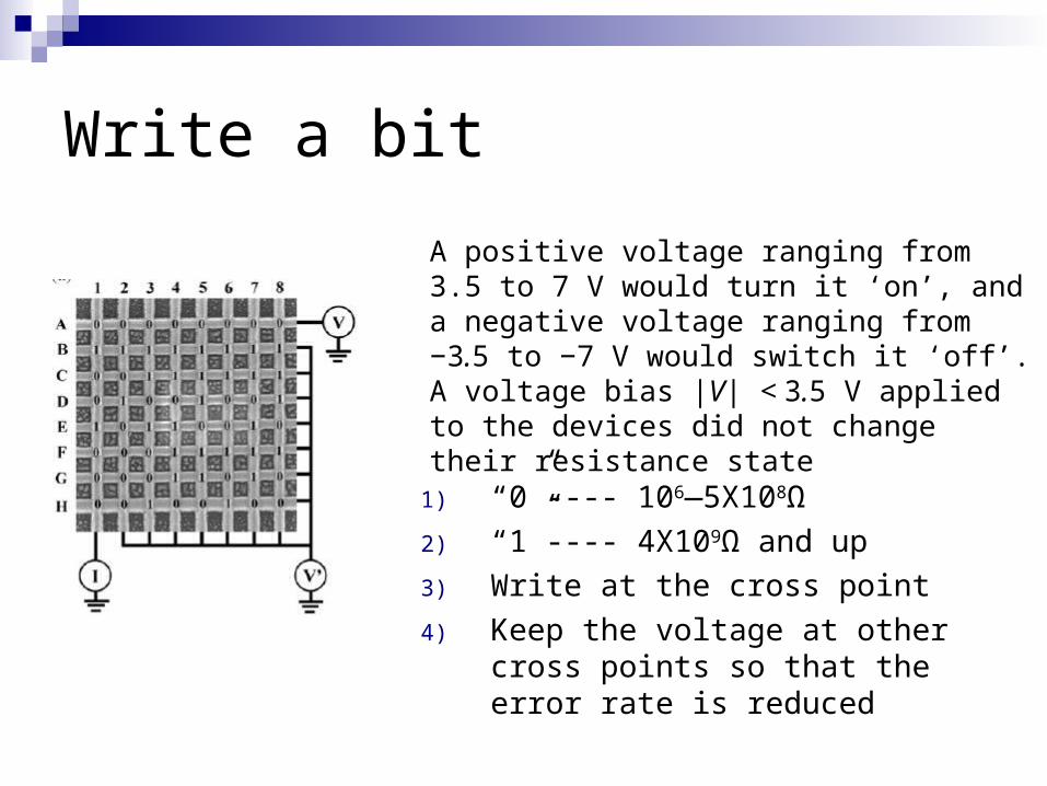
Write a bit
A positive voltage ranging from 3.5 to 7 V would turn it ‘on’, and a negative voltage ranging from −3.5 to −7 V would switch it ‘off’. A voltage bias |V| < 3.5 V applied to the devices did not change their resistance state
1) “0”---- 106—5X10⁸Ω
2) “1”---- 4X10⁹Ω and up
3) Write at the cross point
4) Keep the voltage at other cross points so that the error rate is reduced

Read a bit a bias voltage (much smaller than the voltage used to write the bit)
was applied across the row and column of the bit to be read (e.g. row A and column 1 for reading cross point (1, A) in figure 3(a)), but
all of the other rows and columns were grounded.

Resistivity

Reading current Max reading
current is of the order of 10-10A

Results for 1kbits memory circuits
More condensed nanowires

Read current

Electronic characteristics it shows the process of
turning on and off.
the turning on and off processes don’t overlap with each other.

Limitations The current crossbar memory technology
does not allow for a very large number of write cycles
A voltage magnitude, |V| >=3.5 is needed to change the resistance state between ‘0’ and ‘1’
Lithography used in electrode and connection fabrication
Nanowires are so small that atomic defects are unavoidable and serious

Limitations
Resolution is limited currently to about 30nm half-pitch
Have to build in redundancy to compensate for defects
Range of logic operations that can be performed is limited without the NOT function

Conclusions
Nanoscale crossbar structures show potential in developing new nanoelectronics, especially high density memory and logic
It will take many years before the manufacturing technology reaches the point where the full potential of these structures can be realized

Future Work
Defect Tolerance Improvement of nanofabrication technology
for more reliable, higher density crossbar structures
Look at what materials are best suited for these structures
Increase logic capabilities of the crossbar structure

Summary Nanoscale molecular crossbar circuits can
function as ultra high density memory Demultiplexer/multiplexer logic can be
integrated with the memory using the crossbar structure
There is a lot of interest in the use of nanoscale crossbar structures for use in high density nanoelectronics
More work has to be done to achieve full potential of the crossbar structure