nanolaminated thin films for thermoelectrics - diva portal323672/fulltext01.pdf · during...
TRANSCRIPT

Department of Physics, Chemistry, and Biology
Master’s Thesis
Nanolaminated Thin Films for Thermoelectrics
Sit Kedsongpanya
LITH-IFM-A-EX--10/2296--SE
Thin Film Physics Division
Department of Physics, Chemistry, and Biology (IFM)
Linköping University
SE-581 83 Linkoping, Sweden


Datum
Date
2010-06-02
Avdelning, institution
Division, Department
Division of Thin Film Physics Department of Physics, Chemistry, and Biology Linköping University SE-581-83 Linköping, Sweden
URL för elektronisk version http://urn.kb.se/resolve?urn=urn:nbn:se:liu:diva-56699
ISBN
ISRN: LITH-IFM-A-EX--10/2296--SE
_________________________________________________________________
Serietitel och serienummer ISSN
Title of series, numbering ______________________________
Språk
Language
Svenska/Swedish
Engelska/English
________________
Rapporttyp
Report category
Licentiatavhandling
Examensarbete
C-uppsats
D-uppsats
Övrig rapport
_____________
Titel
Title Nanolaminated Thin Films for Thermoelectrics
Författare
Author Sit Kedsongpanya
Nyckelord Thermoelectric, Thermoelectric figure of merit (ZTm), TiN, ScN, Superlattice, Ca3Co5O9, Nanolaminate, Seebeck effect, Keyword Peltier effect.
Sammanfattning Abstract
Energy harvesting is an interesting topic for today since we face running out of energy source, a serious problem in the world. Thermoelectric devices are a good candidate. They can convert heat (i.e. temperature gradient) to electricity. This result leads us to use them to harvest waste heat from engines or in power plants to generate electricity. Moreover, thermoelectric devices also perform cooling by applied voltage to device. This process is clean, which means that no greenhouse gases are emitted during the process. However, the converting efficiency of thermoelectrics are very low compare to a home refrigerator. The thermoelectric figure of merit (ZTm) is a number which defines the converting efficiency of thermoelectric materials and devices. ZTm is defined by Seebeck coefficient, electrical conductivity and thermal conductivity. To improve the converting efficiency, nanolaminated materials are good candidate.
This thesis studies TiN/ScN artificial nanolaminates, or superlattices were grown by reactive dc magnetron sputtering from Ti and Sc targets. For TiN/ScN superlattice, X-ray diffraction (XRD) and reciprocal space map (RSM) show that we can obtain single crystal TiN/ScN superlattice. X-ray reflectivity (XRR) shows the superlattice films have a rough surface, supported by transmission electron microscopy (TEM). Also, TiN/ScN superlattices grew by TiN as starting layer has better crystalline quality than ScN as starting layer. The electrical measurement shows that our superlattice films are conductive films.
Ca-Co-O system for inherently nanolaminated materials were grown by reactive rf magnetron sputtering from Ca/Co alloy target. The XRD shows we maybe get the [Ca2CoO3]xCoO2 phase, so far. The energy dispersive X-ray spectroscopy (EDX) reported that our films have Al conmination. We also discovered unexpected behavior when the film grown at high temperature showed larger thickness. Therefore, Ca-Co-O material system requires further studies.


"Mankind can not obtain anything without first sacrificing something in return. That is Alchemy's law of equivalent exchange"
by Arakawa Hiromu from “Fullmetal Alchemist” Japanese comic.
Don’t be afraid.

ii
© Sit Kedsongpanya
Figure 4.1 Reprinted with permission from A. C. Masset, C. Michel, A. Maignan, M. Hervieu,
O. Toulemonde, F. Studer, B. Raveau, and J. Hejmanek, Phys. Rev. B 62, 166-175 (2000).
© (2000) by The American Physical Society.
Printed by LiU E-PRESS, Linköping, Sweden, 2010

i
Abstract
Energy harvesting is an interesting topic for today since we face running out of energy source, a
serious problem in the world. Thermoelectric devices are a good candidate. They can convert
heat (i.e. temperature gradient) to electricity. This result leads us to use them to harvest waste
heat from engines or in power plants to generate electricity. Moreover, thermoelectric devices
also perform cooling by applied voltage to device. This process is clean, which means that no
greenhouse gases are emitted during the process. However, the converting efficiency of
thermoelectrics are very low compare to a home refrigerator. The thermoelectric figure of merit
(ZTm) is a number which defines the converting efficiency of thermoelectric materials and
devices. ZTm is defined by Seebeck coefficient, electrical conductivity and thermal conductivity.
To improve the converting efficiency, nanolaminated materials are good candidate.
This thesis studies TiN/ScN artificial nanolaminates, or superlattices were grown by reactive dc
magnetron sputtering from Ti and Sc targets. For TiN/ScN superlattice, X-ray diffraction (XRD)
and reciprocal space map (RSM) show that we can obtain single crystal TiN/ScN superlattice. X-
ray reflectivity (XRR) shows the superlattice films have a rough surface, supported by
transmission electron microscopy (TEM). Also, TiN/ScN superlattices grew by TiN as starting
layer has better crystalline quality than ScN as starting layer. The electrical measurement shows
that our superlattice films are conductive films.
Ca-Co-O system for inherently nanolaminated materials were grown by reactive rf magnetron
sputtering from Ca/Co alloy target. The XRD shows we maybe get the [Ca2CoO3]xCoO2 phase,
so far. The energy dispersive X-ray spectroscopy (EDX) reported that our films have Al
conmination. We also discovered unexpected behavior when the film grown at high temperature
showed larger thickness. Therefore, Ca-Co-O material system requires further studies.


iii
Acknowledgments
This Master’s thesis could not have been realized without the support or contribution of people
during Master’s project work. So I would like to show my gratitude.
• First of all, I owe my deepest gratitude to my supervisor Per Eklund. He is very patient
and wonderful when I always come and ask him for permission to do the experiments
(like father and son when his son would like to play the expensive toy). He always has
good discussion with me (in the scientific way and non-scientific). He always has a good
suggestion and gives exercises for practice everything that he thinks “it is fun!”
• I would like to give my gratitude to my co-supervisor Gunilla Wingqvist for your help
and good discussion all time (and it took very long).
• I owe a big thanks to Agn÷ Žukauskait÷; you help me and teach me how to use Jessie
and non-formal discussion about the language. Especially, she keeps encourage me due
to TiN shot circuited problem that gives me almost miss the beautiful sample for TEM
measurement.
• Thank Ali Khatibi for helping me in RF sputtering in Jessie and a good talk in football.
• I am really grateful to Professor Jens Birch for every Thursday lecture on how to use
Asterix for High Resolution Reciprocal Space Map. Also, a very good discussion and
teaching in superlattice, which is the second thing that you love after your family. The
sentence “you have to think it yourself” always stays in my head.
• This thanks for Thomas Lingefelt for the SEM and EDX teaching, Jun Lu for beautiful
TEM images, Jens Jensen for ERDA measurement.
• Thanks also all other member of the Thin Film Physics, Nanostructured Materials,
Plasma and Coating Physics group for your contribution.
• Thank to my friends who have studied and met me at Linköping University. And a lot of
special thanks to Tom An-Sheng Cheng for helping me speak English quite well today.
Eddy Nai-Yuan Ku for be a good opponent and a nice every discussion group before
exam period past two years.

iv
• I would like to thank Ajan Sukkaneste Tungasmita and Leif Johansson who give such
a big opportunity to study at Linköping University.
• Thank for financial support from “Linnaeus-Palme” scholarship for my study in Sweden.
• I would like to thank Ajan Rujikorn Dhanawittayapol . I know he does not want me to
put his name on this page. However, if I did not have your guidance on that night, I
would not have come to get a very good experience in Sweden.
• Finally, there are a small group of people that I must see at every 4.00 pm and 3.00 pm in
daylight saving every day in front of my laptop. They are my parents and my younger
sister in Thailand who make me laugh every day that give me never homesick. Also,
they encourage, support, and pray for me every day, I have studied in Sweden.

v
Table of Contents
1 INTRODUCTION.......................................................................................................1
2 A BRIEF HISTORY OF THERMOELECTRIC DEVICES........ .............................3
2.1 SEEBECK EFFECT...................................................................................................3
2.2 PELTIER EFFECT....................................................................................................4
2.3 THOMSON EFFECT.................................................................................................5
3 BACKGROUND..........................................................................................................7
3.1 CARNOT’S THEOREM.............................................................................................7
3.2 THERMOELECTRIC MECHANISM.............................................................................8
3.2.1 Coefficient of performance (COP), Efficiency of heat engine (η), and
Thermoelectric figure of merit (ZTm) ...........................................................9
3.2.2 Thermoelectric refrigeration and coefficient of performance (COP)..........10
3.2.3 Thermoelectric generation and efficiency of generator (η) ........................12
3.2.4 Thermoelectric figure of merit (ZTm) – geometrical consideration.............13
3.2.5 Thermoelectric figure of merit (ZTm) for a single thermoelectric material .14
4 LITERATURE REVIEW .........................................................................................17
4.1.1 Complexity through disorder in the unit cell..............................................17
4.1.2 Complex nanostructure approach..............................................................18
4.1.3 Multilayer substructure approach or superlattice approach ......................18
4.1.4 Ca-Co-O and related materials .................................................................20
5 MULTILAYER STRUCTURE AND INHERENT NANOLAMINATE ... .............23
6 DEPOSITION PROCESSES ....................................................................................29
6.1 SPUTTERING........................................................................................................29
6.2 DC MAGNETRON SPUTTERING..............................................................................30
6.3 RF SPUTTERING...................................................................................................31
6.4 REACTIVE SPUTTERING........................................................................................32
6.5 EXPERIMENTAL DETAILS .....................................................................................33
6.5.1 TiN/ScN system .........................................................................................33
vi
6.5.2 Ca-Co-O system........................................................................................34
7 CHARACTERIZATION METHODS ..................................................................... 35
7.1 STRUCTURE CHARACTERIZATION........................................................................ 35
7.1.1 Scanning Electron Microscope (SEM) ...................................................... 35
7.1.2 Transmission Electron Microscope (TEM)................................................ 36
7.1.3 X-Ray Analysis by Scattering Phenomena................................................. 36
7.2 COMPOSITIONAL CHARACTERIZATION................................................................. 42
7.2.1 Energy-Dispersive X-ray Spectroscopy (EDX or EDS).............................. 42
7.2.2 Elastic Recoil Detection Analysis (ERDA) ................................................ 42
7.3 ELECTRICAL CHARACTERIZATION........................................................................ 43
7.3.1 Resistivity measurement............................................................................ 43
8 RESULTS AND DISCUSSION ................................................................................ 45
8.1 TIN/SCN SUPERLATTICES................................................................................... 45
8.1.1 Optimization of TiN and ScN films ............................................................ 46
8.1.2 Characterized TiN/ScN superlattice growth by reactive sputtering............ 53
8.1.3 Electrical properties of TiN/ScN superlattices........................................... 63
8.2 CHARACTERIZATION OF CA-CO-O FILM GROWTH BY REACTIVE SPUTTERING........ 66
9 CONCLUSION ......................................................................................................... 71
10 FUTURE WORK...................................................................................................... 73

1
1 Introduction
“The only way to discover the limits of the possible is to go beyond them into the impossible”
Arthur C. Clarke
Nowadays, global warming and running out of fossil fuels are big issues for people in the world.
Actually, these issues are closely related since global warming or climate change comes mainly
from greenhouse gases, e.g., CO2, CFCs, N2O, etc, which are generated by human activity1.
Starting from the industrial revolution, the fossil fuels are our main energy source; they have
continuously been burned in engines and for heating buildings. Considering that fossil fuels are
unrenewable, running out of fossil fuel is an issue. To solve the problem, we need to find new
sources of energy which are unharmful to the world, renewable, and highly efficient. The
alternative energy technologies are being developed, such as solar cells, hydrogen technology
(fuel cells), wind turbines, etc. To reach higher efficiency, the energy harvesting concept, which
means to capture or store “waste” energy and turn it into useful energy has been involved. The
“waste” energy is the energy that dissipates from generators, i.e., thermal energy, vibration from
heat engine, etc.
Thermoelectric (TE) devices are good candidates in this field because of they can recover heat or
a temperature gradient into electrical energy without any emission of greenhouse gases. Also,
they perform cooling by the reverse process, when they generate a temperature gradient by
applied current. This means that they perform cooling without moving parts and releasing CFCs.
However, the efficiency of cooling and generating electrical energy is low2. Nevertheless, TE
devices have been used in cooling applications; for example microelectronic cooling in X-ray
astronomy or microelectronics that need to operate in low temperature, in generating electrical
energy for vehicles by collecting waste energy from exhaust gas3, and in sensor applications,
e.g., water condensing sensor4.

2
A few decades ago, the “Phonon-Glass Electron-Crystal (PGEC)” concept5 was proposed and
predicted that to achieve high efficiency of TE devices, the materials should have a poor thermal
conductivity and good electrical conductivity. Two types of layered materials have been
suggested that to obey “PGEC” idea, i.e., multilayer or superlattice of metal/semiconductor and
thermoelectric cobaltate. In this thesis, I study the growth of two material systems representing
each of these layered material types respectively.
• First, growth and characterization of thermoelectric multilayer or superlattice which is an
artificial nanolaminate of TiN/ScN on Al2O3 (0001).
• Second, growth and characterization of the thermoelectric cobaltate [Ca2CoO3]xCoO2 on
Si (100) by using reactive RF magnetron sputtering from Ca/Co alloy target.

3
2 A brief history of thermoelectric devices
“History is the version of past events that people have decided to agree upon”
Napoleon
To improve and achieve high efficiency TE devices, we need to understand the mechanism of
TE devices which especially relate to three important effects, i.e., Seebeck effect, Peltier effect,
and Thomson effect (or Kelvin effect).
2.1 Seebeck effect
In 1821, the first thermoelectric effect was discovered by Thomas Johann Seebeck6. Initially, he
proposed that the magnetism of two different metals was generated when the junctions were held
at different temperatures. Later when Ampere's law was proposed, Seebeck realized that he had
misunderstood. Instead of temperature gradient generates magnetism, it produces an
electromotive force (EMF) or voltage in pair of dissimilar metals which can drive an electric
current in a closed circuit. This effect is called Seebeck effect and illustrated in the simple circuit
in Fig. 2.1
Fig. 2.1 A simple thermocouple, TH and TC are the temperature of hot end and cold end, respectively.

4
This effect gives the definition of the Seebeck coefficient (S), often referred to as the
thermoelectric power or thermopower:
( )( ) ,B A H C ABV S S T T S T= − − = ∆ (2.1)
where AB B AS S S= − is the difference in Seebeck coefficients of materials A and B (usually in the
unit µV/K), V is thermoelectric voltage, and H CT T T∆ = − is the temperature difference between
hot end and cold end. If the temperature difference ∆T between the two ends of a material is
small, then
.V
ST
∆=∆
(2.2)
The Seebeck effect is the idea usually used for temperature measurement by thermocouple. To
measure a temperature difference directly or an absolute temperature by setting one end to a
known temperature, the thermoelectric voltage which is produced by heating is scaled up with a
pair of dissimilar metals with known Seebeck coefficients, allowing for temperature to be
determined.
2.2 Peltier effect
In 1834, the second thermoelectric effect was discovered by Jean-Charles Peltier; it is called
Peltier effect6. He showed that cooling occurred when electrical current flowed into a
thermocouple. Heating effect occurred when reverse electrical current was applied. The rate of
cooling (q) at a junction AB when a current (I) is applied from material A to material B, is
obtained by
( ) ,B A ABq I I= Π − Π = Π (2.3)
where AB B AΠ = Π − Π is the difference Peltier coefficients of materials A and B in units of
(W/A). The Peltier effect, however, is quite difficult to determine experimentally due to Joule
heating effect, which occurs when current is passed though metals.

5
2.3 Thomson effect
The relation between the Seebeck and Peltier effects was described by William Thomson (Lord
Kelvin) in 1855, who applied the laws of thermodynamics. He predicted and studied
experimentally the rate of cooling when applying current in a single conductor having a
temperature gradient. This effect is called Thomson effect6, which is the third thermoelectric
effect. The heating or cooling (q) is
,q I Tβ= ∆ (2.4)
where β is the Thomson coefficient of material in units (V/K), I is the current which pass
through the materials, ∆T is the temperature different, and q is the rate of heating or cooling. The
heating or cooling effect depends on electrical discharged of material which gives positive
Thomson effect (+β) or negative Thomson effect (-β). Even though Thomson effect is not
importance in thermoelectric device but it lead to find the relation between Seebeck and Peltier
coefficient
,AB ABS TΠ = (2.5)
and
.AB ABdS
T dT
β = (2.6)
Both are useful for calculating the Seebeck and Peltier coefficient, since we cannot measure the
absolute Seebeck and Peltier coefficient directly. Thomson coefficient can be measured directly.


7
3 Background
TE devices are a kind of heat engine or heat pump. This chapter is going to show how the
efficiency of TE devices can be obtained from thermodynamics and bring us to the
thermoelectric figure of merit, a number that determines the performance of TE devices.
3.1 Carnot’s theorem
The efficiency of heat engines and heat pumps can be obtained from basic ideas in
thermodynamics. The ideally highest efficiency of heat engines were proposed by Nicolas
Léonard Sadi Carnot in 18247, who said that a highest efficiency engine must work in between
hot and cold reservoirs without any loss. This gives Carnot’s theorem:
“No engine operating between two reservoirs can be more efficient than a Carnot’s engine operating between those same two reservoirs”
This assumption can be illustrated in a reversible cycle where the engine will not suffer any
losses, i.e., a cycle must include isothermal* and adiabatic† processes. This cycle is called
Carnot’s cycle. The Carnot’s cycle of a heat engine is shown in Fig. 3.1(a).
Fig. 3.1 (a) shown a Carnot’s cycle in P-V diagram which include two isothermal line connect with two
adiabatic lines, (b) a schematic representation of an engine working in a cycle.
* Isothermal process means the thermodynamic system operates at constant temperature.
† Adiabatic process means the thermodynamic system works without any exchange heat.
(a) (b)

8
The efficiency of heat engine is
.H
W
Qη
∆=
∆ (3.1)
where η is the efficiency of generator, W is energy output from heat engine, and Q is the heat
absorb by the heat engine. The highest efficiency of a heat engine is the Carnot efficiency
1 .C H C
H H
Q T T
Q Tη −= − = (3.2)
The reverse Carnot’s cycle gives the coefficient of performance (COP) of heat pumps:
.HQCOP
W
∆=
∆ (3.3)
where ∆Q is the net heat moved from cold side to hot side (cooling power), ∆W is the net energy
consumed. The Carnot coefficient of performance is
1
.1
C
H H C
C
TCOP
Q T TQ
= =−−
(3.4)
3.2 Thermoelectric mechanism
The thermoelectric mechanism can be explained from heat flow in thermoelectric materials. The
charge carriers (electrons and holes) can diffuse when the material is expressed to a temperature
gradient. Hence, they diffuse from hot end to cold end. The mobile charge carriers will diffuse to
cold side leave behind their immobile element at the hot side thus generating different voltage
between hot and cold side which is called thermoelectric voltage. However, there are some
charged carrier at the cold side can diffuse to hot side. At thermal equilibrium, the rate of
diffusion of hot and cold carriers in opposite directions is equal, which mean there is no net
current in circuit. Due to the imperfection of materials and heat generate lattice vibration
(phonon)‡allow carrier scattering situation giving non-equal charged carrier diffusion. This effect
gives metal behave like n-type and p-type thermoelectric materials which relate to hot carrier or
cold carrier§ is dominate.
‡ This mechanism is called phonon drag (see ref.6) occurs when the phonon-electron scattering predominate in low
temperature condition ( 1 5T≈ ) which give phonon tend to push electron to cold side. § The “hot” and “cold” carriers mean charge carrier which diffused from hot and cold side, respectively.

9
Fig. 3.2 Shown (a) the thermoelectric generating, (b) the thermoelectric cooling diagrams both make from n-
type and p-type thermoelectric materials and connect metal interconnector between them.
The schematic TE devices are shown in Fig. 3.2. They are made from p-type and n-type
semiconductor as thermoelectric materials connected by metal plates. The heat will cause
electrons (in n-type element) and holes (in p-type element) to diffuse to the cold end, creating a
current through the circuit. The Seebeck effect converts the thermal energy into electrical energy.
On the other hand, if a power source is provided, the TE device may act as a cooler. This is the
Peltier effect. Heat is removed from one side of the device into the other side.
3.2.1 Coefficient of performance (COP), Efficiency of heat engine (ηηηη), and Thermoelectric
figure of merit (ZT m)
Thermoelectric devices can work as power generator (Heat engine) or refrigerator (Heat pump)
utilizing the Seebeck or the Peltier process respectively. These processes are in principle
thermodynamically reversible process. Unfortunately, there are also irreversible processes i.e.,
Joule heating (due to electrical resistance in device) and thermal conduction. The actual
efficiency of thermoelectric refrigeration and generation are determined by applied
thermodynamic concepts which give relation to thermoelectric figure of merit (ZTm)6,8-10.
(a) (b)

10
The Tm is the average temperature over the device. Z is dependent on the Seebeck coefficient
(Snp) (which is through the Thomson relations connected to the Peltiter coefficient), the total
series resistance of the device (R) and the total thermal conduction of the device as:
2
,npSZ
KR= (3.5)
In this case, we need to assume no heat resistance between interconnection metals which heat
current from heat sink and source can flow through thermoelectric material perfectly11,12. So if
TE devices would have only reversible process (R→0, K→0), their ZTm value goes to infinity
and their efficiency is the Carnot efficiency.
3.2.2 Thermoelectric refrigeration and coefficient of performance (COP)
The COP of thermoelectric can be calculated by considering simple system as shown in Fig.
3.2(b), thus the net absorbed heat is given in
21,
2np Cq S IT K T I R= − ∆ − (3.6)
where np p nS S S= − is the difference in Seebeck coefficient from each thermoelectric
material, p nK K K= + is the total conductance, p nR R R= + is the series resistance, H CT T T∆ = − is
the absolute temperature different between hot and cold side, and I is a current. The first term is
Peliter cooling, using the Thomson relation (equation (2.5)) to connect Peltier coefficient and
Seebeck coefficient. The second term is the thermal conduction. The last term comes from Joule
heating. So if increasing current, this will increase the Peliter cooling, however, the Joule heating
will dominate since it depends on I2 giving the COP has negative value. By differentiating the
net heat with respect to current, we can find the maximum current as
max .np CS TI
R= (3.7)
This gives the maximum net heat
( )2 2
max
1.
2np C np C
S T S Tq K T
R R
= − ∆ −
(3.8)

11
Next, the electrical power consumes in thermoelectric devices is define by
2 ,npw S I T I R= ∆ + (3.9)
where first term is from thermoelectric effect producing the voltage and the second is electrical
power for external applied voltage. The COP for thermoelectric refrigerator is
( )2 2
2
12
,
np C np C
np
S T S TK T R
R RCOP
S I T I R
− ∆ −
=∆ +
(3.10)
212 ,
C
H C
ZT TCOP
ZT T
− ∆= (3.11)
where Z is thermoelectric figure of merit of thermoelectric devices or materials defined as
2
,npSZ
KR= (3.12)
which will be discuss in later. From equation (3.12), we get maximum temperature difference as
2max
1,
2 CT ZT∆ = (3.13)
Now the alternative condition of particular interest is that maximum coefficient. So the current
that satisfies the condition is defined by
max ,1 1
np
m
S TI
R ZT
∆=
+ − (3.14)
where .2
H Cm
T TT
+=
And using this current calculates the maximum COP as
( )
( )1
.( ) 1 1
C m H C
c
H C m
T ZT T TCOP COP
T T ZTγ
+ −= =
− + + (3.15)
Recall Carnot coefficient of performance is
.C
CH C
TCOP
T T=
−

12
And
( )( )1
.1 1
m H C
m
ZT T T
ZTγ
+ −=
+ +
Thus, the maximum thermoelectric refrigerator efficiency is product of the Carnot cooling
efficiency, which shows the highest thermodynamic theory value for heat pumps and γ is
weight of performance. For example, let us consider the two limiting cases, First ZTm << 1 gives
( ) ( 2)(1 )C H C m H CCOP T T T ZT T T≈ − − which the efficiency is lower that Carnot efficiency.
Second ZTm >> 1 case gives CCOP COP= .
3.2.3 Thermoelectric generation and efficiency of generator (ηηηη)
In order to calculating the efficiency of thermoelectric generator, Let us consider simplest
thermoelectric devices for generating as show in previous section (see Fig. 3.2(a)). For the
energy converting efficiency is obtained like the heat engine (see equation(3.1)). Hence, we
chose load resistance (RL) in appropriate temperature range will give maximum efficiency. This
is shown by Ioffe (see ref.12), he showed the ratio of LR R equal to M which is defined by
1 ,L mM R R ZT= = + (3.16)
where Z is figure of merit, and Tm is average temperature. While, the maximum efficiency is
( 1 1)
,
1
H C mC
HH m
C
T T ZT
TT ZT
T
η εη− + −
= =
+ +
(3.17)
where ,H C
CH
T T
Tη −=
( )
1 1.
1
m
m H C
ZT
ZT T Tε
+ −=
+ +
Therefore, we can see that the maximum thermoelectric generator efficiency is the Carnot
efficiency which is the highest efficiency for heat engine scaling by ε is factor of efficiency
which depend on temperature of heat source and sink and figure of merit. Considering, the
limitation case like in thermoelectric refrigerator ZTm << 1 and. At first limit gives the

13
( )( )2 1H C H M H CT T T ZT T Tη ≈ − + which the Carnot efficiency is factored, giving lower the
efficiency. On the other hand, if ZTm >> 1 it gives H C HT T Tη ≈ − .
3.2.4 Thermoelectric figure of merit (ZTm) – geometrical consideration
Both of thermoelectric generator and refrigerator efficiency depends on the figure of merit as
show in equation(3.15) and (3.17), previously. This section will discuss in detail about figure of
merit (ZTm). Typically, the figure of merit represented as a dimensionless number by multipling
it with average temperature between heat source and sink, hence thermoelectric figure of merit is
written as ZTm. The figure of merit is relation to the properties of materials such as Seebeck
coefficient (S), thermal conductance (K), and electrical resistance (R). As mentioned,
refrigerators operate around 30%-40% of Carnot efficiency that require ZTm equal to 2-42. In
order to achieve mZT >> 1, the product of RK is minimized by reducing the size of
thermoelectric materials. Consequently, one can think that reducing the thermal conduction and
Joule heating increase the figure of merit. However, there are limitations as the result of the
length of material is reduced by increasing cross section. The product of RK is minimize when
the ratio of length and cross section of both sides (formal factor of material) is
1 2
.n p p n
p n n p
L A
L A
ρ κρ κ
=
(3.18)
When this equation is satisfied, it gives the figure of merit of a pair of thermoelectric materials as
( )
( ) ( )
2
21 21 2.
p n
n n p p
S SZ
ρ κ ρ κ
−= +
(3.19)

14
3.2.5 Thermoelectric figure of merit (ZTm) for a single thermoelectric material
Let us now consider the figure of merit of a single thermoelectric material which usually is
represented as:
2
,S
Zσ
κ= (3.20)
whereσ is electrical conductivity,Sis Seebeck coefficient, andκ is thermal conductivity. If we
we can maximize the thermoelectric figure of merit of a material, it will be easier than we
optimize the thermoelectric figure of merit of a device, since we can obtain high thermoelectric
efficiency when combined n- and p-type large ZTm value materials. The individual ZTm value
tells us the thermoelectric efficiency of materials requires high Seebeck coefficient, electrical
conductivity, and low thermal conductivity.
Although we know the requirement of materials for thermoelectric, There are problems in
seeking high figure of merit thermoelectric materials, since the parameters that determine the
ZTm have interrelationship with each other. The electron transport theory lead us to understand
and give possibility to get high ZTm material13. High electrical conductivity can be obtained from
increasing carrier concentration or carrier mobility. Metal is a good candidate, since it has high
carrier concentration. However, the electron-electron scattering cause reducing Seebeck
coefficient of metals. Moreover, metals are half-filled band; they have both electrons and holes
contribution which means that electrons and holes will cancel each other during transported
process lead to get low Seebeck coefficient. According to the simple model (parabolic band,
energy-independent scattering approximation13) the Seebeck coefficient is given by
2 32 2
*2
8,
3 3Bk
S m Teh n
π π =
(3.21)
where Bk is the Boltzmann’s constant, e is the electron charge, h is Planck’s constant, T is a
Temperature,n is the carrier concentration, and *m is the effective mass of the carrier.
Furthermore, electrons and holes also increase thermal conductivity due to thermal conductivity
comes from two sources, electrons and holes transporting heat and lattice vibration (phonon) due
to heat traveling in crystal which the total thermal conductivity is defined as
.e lκ κ κ= + (3.22)

15
For electron thermal conductivity
,e LTκ σ= (3.23)
where σ is electrical conductivity, L is Lorentz factor, and T is temperature. For phonon thermal
conductivity
1 ,3l t mfpC v lκ ρ= (3.24)
where C is the specific heat,ρ is density of phonon, tv is an average phonon velocity, and mfpl is
an average phonon mean free path. While the carrier concentration is raised, the total thermal
conductivity also increase contribute nothing change in thermoelectric figure of merit.
In semiconductor can be optimized a carrier concentration by doping which allows us to achieve
large Seebeck coefficient according to equation(3.21). If we carefully consider the equation,
there is another possibility to increase the Seebeck coefficient, i.e., increasing effective mass.
The band structure of material will affect effective mass of the charge carrier. The effective mass
will be larger when energy bands are flat and narrow close to Fermi energy allows material has
high density of states at Fermi surface. Although the Seebeck coefficient is increased by heavy
carrier, this also reduces carrier mobility since it has low velocity. Typically, the materials have
high effective mass but low mobility which make from covalent bond but in opposite low
effective mass and high mobility make from ionic bond. The semiconductor can also decrease
total thermal conductivity due to reducing carrier thermal conductivity. Hence, the parameters
depending ZTm has relationship with each other. This gives a big issue in optimizing materials
which obtain high figure of merit. Thus, next chapter will discuss about previous developed of
thermoelectric materials are obtained high ZTm.


17
4 Literature review
To obtain good thermoelectric materials, we have to optimize ZTm which depends on S(Seebeck
coefficient), κ (total thermal conductivity), and σ (electrical conductivity). Improved ZTm by
changing properties of material, for example by doping to increase number of charge carriers,
changing structure of materials to reduce phonon thermal conductivity giving Complexity
through disorder in the unit cell and Complex Nanostructure approach concept, or by generating
designable band structures in heterostructures produce high mobility result in Multilayer
substructure approach or superlattices approach, etc. This section is a review of previous work
in research and development of the fabrication of thermoelectric materials with high figure of
merit.
4.1.1 Complexity through disorder in the unit cell
In 1950s, there were a lot of investigation works into semiconductor materials in order to
improve the efficiency of thermoelectrics. The first promising TE materials were found by H. J.
Goldsmid and R. W. Douglas i.e., Bi2Te3 since it had high ZTm at near room temperature (∼290
K)14 which is called low temperature TE material. Bi2Te3 can be doped with Sb2Te3 or Bi2Se3 to
get n-type and p-type thermoelectric materials, respectively13,15. For (Sb0.8Bi0.2)2Te3, which is p-
type, the ZTm values are in range 0.8 to 1.1 because of the inducing point defect by alloying. This
makes increasing of phonon-phonon scattering in U-process (Umklapp process)8 which lowers
the momentum of phonons. As the result of this, the phonon thermal conductivity is reduced. In
spite of this effect, the issue at operating temperature around 300K or higher is that the mobility
is not high enough to maintain good figure of merit due to electron-phonon scattering.
There followed much research on compound tellurides aiming to improve ZTm values. Examples
are PbTe, GeTe, SbTe or SnTe, the ZTm peak in optimized at 0.8 for n-type material13 at
temperature around 300-700 °C (mid-temperature TE materials). For high ZTm p-type is
(AgSbTe2)1-x(GeTe)x or TAGS-x, where x is composition of (GeTe) modules with the highest
ZTm when x = 85 giving ZTm equal to 1.213,16-18. Another approach to reach high figure of merit is
by introducing disorder within the unit cell for example in skutterudies (e.g. CoSb4, IrSb4)8,11,19-21
or clathrates structure (e.g.Na8Si46, Ga16Ge30)8,11,22. In skutterudies structures, a disorder structure

18
is formed by CoSb4 in which a structure is called ‘cage’ or ‘host’ matrix. The disorder makes an
“open structure” like interstitial sites, or partial occupancies. The atoms are filled in the
vacancies, are called ‘rattling’ or ‘guest’ atoms which are the rare-earth elements (e.g. La, Fa,
Zn, Cd, etc.). The total thermal conductivity is reduced due to coupling of cage vibration mode
and rattler vibration mode22. However, their ZTm values are lower than Bi2Te3 since the heavy
atoms generate high carrier concentrations which increase electron thermal conductivity.
4.1.2 Complex nanostructure approach
In 1960s, Si-Ge alloys were found to be good candidates for high ZTm at high temperature (∼1000
°C) with ZTm values around 0.938 and 0.505 for n-type and p-type materials, respectively12,13,23.
Why do n-type Si-Ge alloys have high ZTm values? This is explained by several properties in Si-
Ge alloys: (i) in high temperature regime, Si-Ge alloys have a high carrier concentration that is
generated by thermal energy; the total thermal conductivity will be reduced by electron-phonon
interaction, (ii) the total thermal conductivity of Si and Ge significantly drop when temperature
raises up above 900 °C, (iii) the Si-rich alloys have high melting points compatible with
thermoelectric application, (iv) the electronic structure of Si and Ge since the conduction band of
both materials is highly degenerate resulting in increasing of effective mass give a large Seebeck
coefficient as mention in section 3.3.3.23. Moreover, the total thermal conductivity can be
reduced by Si-Ge polycrystalline alloys, because of grain-boundary phonon scattering.
The good performance of Si-Ge thermoelectric materials is therefore because of their
nanostructure enhances ZTm. To achieve high ZTm material, one should introduce some crystal
defect that scatters phonon to reduce total thermal conductivity without interrupting charge
carrier motion. The idea of “Phonon-Glass Electron-Crystal (PGEC)” was introduced by G. A.
Slack (see ref.5). This idea means that materials with good ZTm value need to have poor phonon
conductivity which gives phonon thermal conductivity like a glass; while they should also have
good electrical conductivity, like a crystal, within the same material.
4.1.3 Multilayer substructure approach or superlattice approach
In the early 1990s, L. C. Hicks calculated and predicted that one could obtain high figure of merit
materials due to quantum confinement of electron charge carriers in a quantum well structure24.
In 1997, G. D Mahan proposed that the best thermoelectric should have high density of state
(DOS) in narrow bands (∼10kBT) close to Fermi level25. Both results suggest that materials

19
having narrows electron energy bands, high density of state, and high effective mass could have
potential to increase the ZTm value. By using quantum wells, narrow bands are obtained and
thermal conductivity of superlattices can be very low due to phonon scattering at the interfaces 26. Thus, a superlattice or “nanolaminate” approach brings us closer to a “phonon-glass” while
maintaining “electron-crystal”. I would like to separate this discussion in two topic i.e.,
thermoelectric multilayer superlattice or artificial nanolaminate and thermoelectric cobalt oxide
(cobaltate) or inherent nanolaminate. I will explain more about the concepts of “artificial” and
“inherent” nanolaminate in next chapter.
The multilayer superlattice hypothesis was corroborated by Rama Venkatasubramanian et al. in
200127. They made Bi2Te3/Sb2Te3 superlattice with remarkably high ZTm~2.4, at room
temperature. The total thermal conductivity of these superlattices decreased due to phonon
scattering at interface, which corresponds to the result Hicks predicted in 1993. So this is good
candidate for “phonon blocking” material. Recently, some theoretical and
experimental28,29attempts to investigate metal-based thermoelectrics failed because of the high
thermal conductivity and also decreased Seebeck coefficient. On the other hand, if one can
optimize the carrier concentration of a metal-base TE there is a possibility to increase ZTm. An
approach around this is to use electron filter consisting of a highly degenerate superlattice with
tall barrier and non-planar barrier (e.g. the tall barrier ∼10.68 eV gives ZTm ≈ 6.8)30, where only
hot electrons* can participate in conducting current. ZrN/ScN superlattice were simulated using
electron filter hypothesis done by M. Zebarjadi et al. in 200931. ZrN has a bulk electrical
resistivity of ρ = 24 µΩ cm at room temperature32 which high melting point of 2980 °C. ScN is a
semiconductor which a direct band gap at theX point in the range of 2.1 eV, while indirect band
gap at Γ→X in the range of 0.9-1.6 eV33-35, and has a high malting point (∼2600 °C)36. The
theory predicted that the ZTm value for this material can be 3 at a temperature of 1200 K32. The
ZTm value is limit by too high barrier height giving low electrical conductivity. They suggested
that one need to optimize barrier height by alloying metal barrier or varying the concentration of
semiconductor.
Experimentally, it has been shown that the total thermal conductivity of ZrN/ScN and
(Zr,W)N/ScN multilayer and superlattice on MgO (100) is gently reduced to compared to
(Zr,W)N alloy32. The results reported that (Zr,W)N/ScN superlattice with film thickness 4.1 ± 0.2
* Hot electrons mean electrons that have high energy from absorbed thermal energy.

20
nm and 2.0 ± 0.2 nm for Zr1-xWxN and ScN, respectively give the lowest total thermal
conductivity at 58% W concentration equal to 1.8 W/(m K) due to multilayer effect and also by
introducing W impurity. So the metal/semiconductor nitride superlattice has possibility to reduce
total thermal conductivity to approximately 2.0 W/m K32. From this result, one can imagine the
superlattice metal/semiconductor to maybe like PGEC materials for promising high-performance
thermoelectric materials. In this thesis, TiN was chosen due to the barrier high adjustment
suggestion30,32. TiN has a NaCl-type rocksalt structure and has an electrical resistivity of 13-15
µΩ cm33,34,37. Moreover, There are some previous work on ScN growth on TiN33.
4.1.4 Ca-Co-O and related materials
The cobaltite oxides system are exciting candidate to improve thermoelectric efficiency. The
cobaltates were interesting to researchers since the discovery of the high-temperature
superconductors (HTSC’s) based on copper oxides (CuO2)38. For HTSC’s, NaCo2O4 was
synthesized with the idea to replace copper with cobalt that would give increased transition
temperature. However, the result showed opposite and further, NaCo2O4 has larger Seebeck
coefficient than HTSC’s while, it has low electrical resistivity as HTSC’s38. More examples of
cobaltates are (Na,Li,Sr)xCoO2 or Ca3Co4O9 or more general [Ca2CoO3]xCoO2 which have been
reported to show that thermoelectric power factor(PF = S2σ) approximately 1.0 × 10⁻³ to 4.5 × 10⁻⁴
W/(m K2) and have total thermal conductivity 1.5 mW/(m K) at 300 K39,40. Considering the
crystalline structure of cobaltates along the [001]-direction, there are metallic-like layers,
consisting of covalently bonded Co-O, separated by insulating; disordered layers with partial
occupancies. Therefore, one can think that the cobaltates have inherently (by nature) a
nanolaminated multilayer structure which highly corresponding with “PGEC” concept.
The result NaxCoO2 and [Ca2CoO3]xCoO2 gave promising thermoelectric properties and it leads
to increased research on materials such as SrxCoO2, LixCoO2 or CaxCoO2 which are called
AxCoO2 (A = Na, Ca, Sr, etc)39 and more complex solid solutions such as Bi2.2-xPbxSr2Co2Oy41,
La1-xCaxCoO3, or La1-xCaxMnO340. NaxCoO2 (x = 0.3 – 1) has a hexagonal lattice with lattice
parameters of a = 0.284 nm, c = 1.081 nm. The [Ca2CoO3]xCoO2 crystal contains alternate stacks
of CdI2-type CoO2 layer and rock-salt-type Ca2CoO3 layer along c axis giving monoclinic42.
Cross section TEM shows the inherently nanolaminated structure of both materials (see
Fig. 4.1).

21
(a) (b)
Both materials have been fabricated with three methods where reactive solid-phases epitaxy
were reported, such as, topotactic-ion exchange39, pulsed laser deposition (PLD)43,44, and RF
magnetron sputtering45. The cobaltate system is an exciting challenge to study as well as need to
understand for high efficient thermoelectric materials.
Fig. 4.1 TEM images of inherent nanolaminate of (a) AxCoO2 where A is a Ca, with periodic 10.7 Å (arrows
indicate the bright AO layer with the dark Co are layer, (b) [Ca2CoO3]xCoO2 with periodicity 36.5 Å. From
ref.46 © (2000) by The American Physical Society.


23
5 Multilayer structure and inherent nanolaminate
Design is not just what it looks like and feels like. Design is how it works.
Steve Jobs (1950-)
Multilayer materials* are known as an artificially structured material, manmade material or
reproducibly manufactured layered structure. Modern thin film techniques are at a stage at which
it is possible to fabricate these structures by depositing two different materials (A/B) from
control able sources which give a periodicity along grow direction where layer thicknesses dA
and dB, are down to one or two monolayer in nano-scales. This technique can create new
materials with unusual properties due to generate new electric structure. The periodicity Λ = dA +
dB is shown in
Fig. 5.1. The multilayer material gives the possibility of engineering new desirable properties
into materials.
Fig. 5.1 Schematic drawing of superlattice where Λ is a period thickness.
Superlattice is a word to describe multilayer structure with periodicity small enough to give
satellite feature in X-ray diffraction pattern (see Fig.5.2). In Fig. 5.1 the two different materials
are stacked along z direction (growth direction) which can be treated as a one dimensional model
layered structure.
* This topic rely on ref.47,48.

24
Fig. 5.2 The XRD pattern of (a) 180 nm thick ScN grown on 120 nm thick TiN which have two peaks
corresponding to ScN 111 and TiN 111, and (b) ScN/TiN multilayer of 30 nm bilayer in each layer
approximately 30 nm thick grown on TiN seed layerwhich shows superlattice satellite features.
The diffraction peaks position is generally determined by Bragg’s law, however, the intensity is
weighted from structure factor F(Q) and Laue function ( )NL Q
2
( ) ( ) ( ),NI Q F Q L Q= (5.1)
where
sin( 2)
( ) ,sin( 2)N
N QL Q
Q
Λ= Λ (5.2)
2 2
2
0
( ) ( )exp( ) ( )exp( ) .n nn
F Q z i dz f Q iρΛ
= ⋅ = ⋅∑∫ Q z Q z (5.3)
Here the Λ is the periodic thickness, the ρ(z) is the electron charge density of superlattice, Q is
scattering wave vector, and fn(Q) is atomic scattering factor in n-th plane.defined by
,
0
( ) ( ) exp( ) .A BD
zf Q z i dzρ= ⋅∫ Q z (5.4)
The electron charge density function of superlattice is described in step model according to
stacking two different materials along z direction, which is generated from modulation of bilayer
stacked superlattice which shown in Fig. 5.3(a). Thus, the electron charge density of superlattice
is a periodic function. In this case, Laue function is calculated from the Fourier transform of

25
periodic step function in real space. It gives Laue function in term of a set of delta function in
reciprocal space. Therefore, one can see satellite or reflected feature on X-ray diffractogram.
However, the periodic delta function will be modified by the atomic scattering factor which is
generated by a Fourier transform of electron charge density of individual material in superlattice
but each material has its periodic electron charge density function (see Fig. 5.3(b)). So the
equation 5.3, the structure factor of new periodic condition is a convolution of two periodic
functions, which is defined by:
( ) [ ]2 1 22 2( ) ( ) 2 ( ) ( ) cos( 2),A A B B A B A BF Q f L Q f L Q f f L Q L Q Q= + + Λ (5.5)
where LA(Q) and LB(Q) are the individual material Laue function.
Fig. 5.3 (a) One-dimensional electron charge density model of superlattice with a perfectly periodic structure.
The N bilayers is stacked in z direction which Λ = DA + DB is a period of superlattice, (b) Modified one-
dimensional electron charge density model of superlattice which is given by individual electron charge density.
If the thickness of both material is small enough, the result of convolution two periodic function
gives diffraction intensity correspond to arithmetic average lattice spacing of two alternate layers
d . The intensity which is obtained from the structure factor convolute with Laue function, gives
(a)
(b)

26
a satellite pattern in XRD pattern. Therefore, the artificially structured materials is called
“superlattice” †. From the XRD pattern, we can calculate the period of superlattice by
( )1
,2 sin sinn n
nλθ θ ±
−Λ =−
(5.6)
where λ is the X-ray wavelength and the integer n is the order of superlattice satellite locate at
θn. Multilayer structures can be used in many applications as a result of their remarkable
electrical, optical, and mechanical properties. For example, they are used in electronic as high
electron mobility transistors, multiple quantum well lasers or waveguides. In optical and
mechanical properties, metallic superlattices are used for UV- or soft X-ray mirrors, magnetic
recording heads, wear protective coatings, etc
The term “Inherently nanolaminate” structure50 is used to describe materials with substructures
that are multilayer structure by itself not artificial design like first case which the individual
layers are in the nanometer scale or in atomic range. Good example for this structure is MAX
phases materials which is ternary carbides or nitrides which are a class of hexagonal-structure.
By anisotropic hexagonal-structure of MAX phase material, if they are seen in cross section
transmission electron microscope (TEM), they show nanolaminate as shown in Fig. 5.4
Fig. 5.4 the cross section TEM image of Ti3SiC2, showing twinning and the characteristic “zig-zag” stacking
of MAX phases. Image took from ref.50, corsetry of P. O. Å Persson.
This structure gives remarkable properties for MAX phase that is the combination of metallic
and ceramic properties. The reason of these properties is TiC or MA which is exhibit highly
ceramic properties since between Ti and C layer have Si layer is inserted that give increasing of
† More detailed descriptions can see in ref.49.

27
Ti-Ti bond by C has to make bond with Si. Additionally, the cobaltate also have inherently
nanolaminate structure which I would like talk in details in previous section.


29
6 Deposition processes
In vapor deposition of thin films*, the films are grown by combination of “building blocks”.
These building blocks are free particles of elements in vapor phase which condense into solid
phase and deposit on a surface as film. How are those free particles formed? And how can the
film be grown? There are two main approaches: physical vapor deposition (PVD) and chemical
vapor deposition (CVD). In chemical vapor deposition, the films are grown on the substrate (the
object we need to coat) by chemically reacting gases. For physical vapor deposition, the vapor
phase originates from a solid or liquid which is thermally evaporated or sputtered. These free
particles are transported to and grown on the substrate. In this chapter, I would like to describe
sputter deposition, which I have used to synthesize material in this thesis.
6.1 Sputtering
“Sputtering” is a method which ejects particles of material from a solid surface (known as
target). The impact of energetic ions are used (often Ar+) to eject or sputter the particles from
target. The sputtered particles are transported to the substrate where they condense and form
film. A schematic sputtering setup is shown in Fig. 6.1(b).
Fig. 6.1 (a) Shows sputtering process at surface of target, (b) Schematic drawing of sputtering setup.
This sputtering setup is called diode sputtering. To get good quality of films, ultra high vacuum
(∼10-9 torr) is often needed to avoid contamination in films. To produce energetic ions, argon gas
or another noble gas is fed to the chamber as sputter gas at pressures of 10-3 mbar to 10-1 mbar.
After that, a negative dc voltage is applied to the target (cathode). The sample holder and
* This chapter is based on the Materials Science of Thin Films by M. Ohring51.
(a) (b)

30
chamber walls act as anode. The argon gas is ionized. The argon ions will be accelerated to
sputter atoms at the target; sputtered species will deposit on the substrate. The substrate is placed
in a substrate holder; that can be electrically biased, grounded, or floating; cooling or heating
also can be applied. Sputtering is widely used for coating in both research work and industrially.
There are many modes of sputtering ,e.g., use of reactive gases during process (known as
reactive sputtering), the use of magnets behind target, called magnetron sputtering†, and different
applied voltage forms. For example, direct current (DC magnetron sputtering), radio frequency
(RF magnetron sputtering), or high-power impulse (High-Power Impulse Magnetron Sputtering,
HiPIMS). In this thesis, I use reactive DC magnetron sputtering and reactive RF magnetron.
6.2 Dc magnetron sputtering
DC magnetron sputtering technique uses an applied magnetic field to trap outgoing electrons
close to the target in order to enhance the sputtering efficiency. The main concept behind this
method is the interaction of charged particles with electromagnetic fields as given by the Lorentz
force
( )d
m edt
= = + ×vF E v B , (6.1)
where e is the electronic charge, m is the particle mass, here is electron mass, v is the velocity, E
the electric field and B the magnetic field. If the vector product ×E B is not equal to zero, this
produces a circular drift electron motion.
A magnetron applies a static magnetic field located parallel to the target (cathode) surface. Due
to electric field between sample holder (anode) and target, this electric field will generate
electron loop motion parallel to the cathode surface. Ionization occurs according to
0 2e Ar Ar e− + −+ → + . (6.2)
This means that electron impact with neutral Ar atoms can generate Ar+ ions. This is the main
process to maintain plasma discharge. So, one needs to increase ionization process (probability
of electron collision with Ar atoms) in order to maintain sputtering. For this purpose, the
secondary electrons, which are produced during ion bombardment (see Fig. 6.1(b)) are confined
† Non-magnetron sputtering is seldom used except for sputtering of magnetic materials, nowadays.

31
by the field from the magnetron. In addition, confinement of the plasma close to target will
increase sputtering rate or deposition rate as shown in Fig. 6.2. Therefore, this technique is used
in both research and industrial production since it has much higher deposition rate (can be 10
time higher) than diode sputtering.
Fig. 6.2 Schematic drawing DC magnetron sputtering increase ionization in plasma which show race-track
region.
6.3 Rf sputtering
Sputtering from insulating targets tends to be complicated, if we use dc sputtering. By applying a
radio frequency alternating voltage supply to the insulating target, sputtering is possible. To be
compatible with plasma sputtering the radio frequency can be chosen in the range 5 MHz to 30
MHz. However, there are many instruments that use radio frequencies, which can cause jamming
problem. The Federal Communications Commission state that 13.56 MHz is reserved for plasma
processing. This kind of sputtering is called RF sputtering.
RF sputtering is a powerful method for sputtering insulating targets. Because of the negative
self-bias of the target, sputtering is possible. The insulating target acts like a capacitor; it will
charge and discharge in cycles of alternating voltage. Additionally, the target does not allow dc
currents to pass through. The self-bias is caused by the fact that the electrons have considerably
higher mobility than the ions, when a large electron current flow to a target at positive half cycle.
Thus, the net current to target must be zero in each RF cycle, the target must develop negative dc
self-bias offset relative to the plasma potential, giving zero net current at steady state.
But this phenomenon also occurs at the substrate. Therefore, electrons oscillate following RF
bias which is disadvantageous for RF sputtering and results in low deposition rate. This can be
avoided by increasing the size of sample holder or electrode on this side larger than the target

32
size; which can reduce the negative self-bias voltage. Unfortunately, we still have problem with
low deposition rate; a more effective way is to use pulse dc.
6.4 Reactive sputtering
Sputtering of compounds has issues with the stoichiometry of films, as result of a loss of certain
species. While sputtering from oxide targets, oxygen tends to be lost during the deposition
process. In order to obtain good stoichiometric growth, reactive sputtering is preferred. This
technique uses sputtering from metallic target in reactive gas ambient. The target vapor phase
species will react with reactive gas when they arrive at the substrate surface and form compound
films. Reactive sputtering is widely used for growth of oxides, nitrides, or sulfides for example.
Fig. 6.3 The deposition rate as a function of reactive gas flow. It is shown hysteresis behavior in reactive
sputtering where fre is a recovery reactive gas flow and fcri is a critical reactive gas flow.
In Fig. 6.3 shows the so-called hysteresis curve of deposition rate against reactive gas flow rate
that occurs during reactive sputtering of metallic targets. There are two different deposition
modes, metallic mode and compound mode which affect the deposition rate. In metallic mode,
the sputtering system has a lot of metallic species than reactive gas, so film is deposited at very
high rate (see Fig. 6.3). This situation will maintain until reach unstable reactive gas flow point
which is called the critical flow point (fcri). If we still increase flow above this point, the
deposition rate will suddenly drop in non-linear or avalanche phenomenon. The extra reactive
gas will form insulating sheet on top of target reduced bias voltage of target (called target
poisoning). As a result low Ar+ ions bombard the target. This situation cannot reverse back to
metallic mode easily by reducing reactive gas flow. As the system has residual reactive gas

33
which sticks at all chamber surfaces, target, and substrate, time is needed for metallic species
consume reactive gas then the deposition rate will back to metallic mode at the recovery reactive
gas flow (fre).
In order to prevent or reduce this situation, one can charge the supply cathode voltage from DC
to RF due to RF sputtering is compatible with insulator, so when the target is poisoning the
sputtering process will continue with a little change. Another useful method is partial pressure
feedback control of the reactive gas.
6.5 Experimental details
6.5.1 TiN/ScN system
Multilayer TiN/ScN films were grown on Al2O3(0001) substrates using reactive magnetron
sputtering in two-chamber consist of a sample introducing chamber working at low vacuum
regime 1x10⁻⁶ Torr (1x10⁻⁴ Pa) and four-target compatible magnetrons growth chamber with a
base pressure in 1x10⁻⁸ Torr (1.3x10⁻⁶ Pa). The sputtering target disks have 5 cm diameter. The Ti
and Sc targets have 99.9% purity. The depositions were performed in Ar/N2 ambient with the
total gas pressure at 1.4 x10⁻³ Torr were measured by capacitance manometer. The flow rate were
maintained constant by mass-controller at 22.0 SCCM for Ar (the unit SCCM is cubic centimeter
per minute at STP) and 3.3 SCCM for N2, respectively. During deposition, the power-regulated
dc power supplies were used to control compositions in 100 - 125 W for TiN and in 60 - 120 W
for ScN. To obtain multilayer films, Ti and Sc target were alternately closed in different period
of time by manually control shutters. The deposition temperature was maintained at a
temperature range of 750 - 800 °C during deposition which was determined by pyrometer. The
substrate was also rotated during deposition in order to obtain uniform film.
The substrates were polished Al2O3 wafers at side where film was deposited. They were cut in 11
x 11 x 0.45 mm3 with protective tape at both sides to avoid dust on surface during cutting. Prior
to deposition, substrates were degreased in ultrasonic bath of trichloroethane, acetone, and
isopropanol, after that blown dry with dry N2. Then they were mounted on solid sample holder
plate, which is made from flat solid Mo with clamping to attach sapphire substrate. The holder
with substrate was inserted into introducing chamber for transfer to deposition chamber. For
final substrates preparation, they were degassed by heating at 1100 °C (determined by

34
thermocouple). A 100 nm thick TiN bottom-electrode layer was grown in order to measure cross-
plane electrical properties. After that, these samples were mounted on another sample holder
using for TiN/ScN multilayer growth which is made from solid Mo plate with a hole in a middle
of the plate where substrate is put in.
6.5.2 Ca-Co-O system
The Ca-Co-O thin films were prepared by reactive rf magnetron sputtering in the same vacuum
system which used in previous growth (TiN/ScN films). The composite Ca/Co with 99.9% purity
had used as a sputtering target which had 5 cm diameter. Sputter deposition was performed in
flow control mode of Ar/O2 mixing atmosphere of pure Ar, 3% of O2 flow, and 5% of O2 flow,
respectively with varied total flow, i.e., 71.2 SCCM and 104.2 SCCM. During deposition, the
power-regulated power supplies were used at 100 W. The deposition temperature was
maintained at a temperature range of room temperature to 700 °C. The substrate was also rotated
during deposition in order to obtain uniform film. Single crystal Si (100) was used as the
substrates. They were cut in 17 x 17 mm3. Prior to deposition, substrates were degreased in
ultrasonic bath of trichloroethane, acetone, and isopropanol, after that blown dry with dry N2.
Then Si substrate was mounted on Mo plate with a hole, which the same model as use for
TiN/ScN multilayer growth. The sample holder with substrate was inserted into introducing
chamber for transfer to deposition chamber.

35
7 Characterization methods
Your equipment DOES NOT affect the quality of your image. The less time and effort you spend worrying about your equipment the more time and effort you can spend creating
great images. The right equipment just makes it easier, faster or more convenient for you to get the results you need.
Ken Rockwell, Your Camera Does Not Matter, 2005
This chapter will discuss and describe the characterization techniques that I have used in this
thesis.
7.1 Structure characterization
7.1.1 Scanning Electron Microscope (SEM)
SEM52 is a technique that acquires three-dimensional topographical surface images of a sample.
SEM uses electrons instead of light, which results in higher resolution and depth of field
compared to Optical Microscope (OM). SEM is analogous with the reflective mode of OM but
uses a focused electron beam that is scanned over the surface of sample. A detector collects the
result of the interaction between the electron beam and the sample, e.g., secondary electrons
(SE), X-rays, backscattered electrons (BSE), etc. The most common modes are imaging is
secondary electrons (SE) mode, in which the surface topography is obtained by secondary
electron contrast and backscattered electrons (BSE) that are used to both compositional contrast
and topographical contrast. SEM is a simple method to understand topographical surface of the
sample and does not require much time in sample preparation process. It is also easier to handle
than Transmission Electron Microscope (TEM). However, SEM has lower resolution compared
to TEM. In this work, SEM LEO which acceleration voltage 5 keV was used for surface
topology characterization of TiN bottom electrode. Also it used to thickness of the Ca-Co-O
sample from cross-section SEM images.

36
7.1.2 Transmission Electron Microscope (TEM)
TEM52 is widely used for investigation of microstructure and composition of materials down to
atomic scale (below 1 Å). TEM uses high energy electron beam typically the acceleration voltage
above 100 keV which is higher than SEM. So that TEM provides very high resolution and large
depth of field compare to SEM. TEM works similar as transmission mode in OM. The electron
beam is focused by electromagnetic lenses to penetrate very thin sample (< 50 nm). The
scattering between the electron beam and the sample gives crystallographic information due to
electron diffraction patterns in reciprocal space and the sample image in real space. Therefore,
the sample is must be very thin, sample preparation is a time consuming, and the instrument is
expensive. But TEM is a powerful and useful tool for materials analysis, and gives information
very difficult to obtain in any other way.
7.1.3 X-Ray Analysis by Scattering Phenomena
X-ray scattering in crystals53, if it obeys momentum conversation law, is described by
diff inc− =k k q (7.1)
where k inc is incident X-ray wave vector which inc
2πλ=k , kdiff is diffracted X-ray wave vector
which the elastic scattering condition inc diff=k k , and q is scattering wave vector or momentum
transferred to crystal. Constructive diffraction (reflection) occurs when the scattering wave
vector is equal to the reciprocal lattice vector (Ghkl) give us the relation
hkl=q G (7.2)
where 2
ˆhkl
hkld
π=G n , where hkld is the distance between lattice planes indicate by Miller indices
(hkl) and n is unit vector perpendicular with (hkl) lattice plane. Furthermore, the reciprocal
lattice vector (Ghkl) is a vector which defines lattice points (coordinate) in reciprocal space where
the coordinate is given subscript set of the coordinate hkl. In Fig. 7.1 shows a circle corresponds
to 2D-Ewald sphere, the sphere can be draw by using Ewald construction. This method helps us
to understand Laue condition and reciprocal space. The construction is started from drawing a
sphere, which the radius equals to inck to a reciprocal lattice point. If the sphere coincides with
another point, the difference between two points will equal to Ghkl; this sphere is called Ewald
sphere.

37
Fig. 7.1 Shows schematic drawing of Ewald circle is constructed by incident X-ray is reflected from sample
which fully fill ksca = k inc + G.
According to Ewald is construction principle, the simple X-ray diffraction measurement can be
preform. If the incidence angle ω is equal to a half of the diffracted angle θ, and the angle
between the incident beam and the detector 2θ are scanned. This scans is called symmetric 2θ
scans or conventional θ-2θ scans see Fig. 7.2(a).
Fig. 7.2 Illustrate X-ray scattering and momentum transfer in different condition (a) symmetric θ-2θ scan, and
(b) “rocking” curve ω-scan.
(a) (b)

38
The incident beam is set equal to θ and the angle between incidence beam and scattered beam
will equal to 2θ. The magnitude q is changed during scanning with direction perpendicular
sample surface. Again, if the scattering follows Laue condition,
2 22sin
2 sin
hkl
diff inc hkl
hkl
hkl
d
d
π πθλ
θ λ
=− =
=
=
q G
k k G
(7.3)
This recovers Bragg formulation and the reciprocal lattice point from Ewald construction. It
indicates Bragg peak positions which mean it gives the X-ray diffraction in reciprocal space. On
the other hand, If ω is scanned and 2θ is fixed, this type of scan is called “rocking” scan (see.
Fig. 7.2(b)) where the magnitude q is constant but it changes in direction. The ω-scan is done by
keeping constant between the angle of X-ray source and detector, while the sample is rocked
around source and detector. The ω-2θ scan is quite similar to θ-2θ scan but instead of setting ω =
θ, this scan will change ω in small amount after that measuring 2θ scan on each step which gives
different magnitude and direction of q. So this method is called asymmetric 2θ scan. By such a
scan the 2-D reciprocal space will be mapped.
7.1.3.1 X-ray Diffraction (XRD)
In thin film work, XRD52 is one the most useful techniques to characterize the structure of films.
XRD is used to identify the crystalline phases in a sample; structural properties can also be
accurately determined: strain state, grain size, epitaxy, preferred orientation, and more. This
technique is based on Bragg’s law:
2 sinn dλ θ= (7.4)
where n is an integer corresponding to order of diffraction, λ is the wavelength of the X-ray
source, d is the distance between atomic planes, θ is the angle between the incident beam and the
atomic plane. By diffraction of X-rays, there is a set of possible peaks depending on the crystal
structure. The most common mode is θ-2θ scans. Here, the detected peaks in the diffraction
pattern are used to identify the crystalline phases present in the sample. The present work
structural characterization of as deposited films was performed by X-ray diffraction (XRD) using
CuKα1 as X-ray source with diffraction θ-2θ scans which employing by a Philips X’pert system
was used.

39
7.1.3.2 X-Ray Reflectivity (XRR)
The thickness of films can be measured by X-Ray Reflectivity (XRR) which is performed in the
same way as XRD with small angle region. The thickness of the film is calculated from the
modified Bragg’s law:
2
2
12 sin 1 ,
sin
nm dλ θ
θ−= + (7.5)
where m is the order of Bragg reflections,n is the average refractive index of the film. From
measurements of low angle X-ray reflectivity (Fig. 7.3), one can calculate film thickness (d)
from equation 7.5
Fig. 7.3 X-rays reflectivity measurement for ScN on Al2O3 which shows sequential interference of X-rays is
called Kiessig fringes.
This method is also used to measure periodicity of multilayer thin films (Λ) according to
2
2
12 sin 1 .
sin
nmλ θ
θ−= Λ + (7.6)
The low angle reflectivity curves from multilayer thin films are more complicated than
individual layers. The curves have Bragg peaks due to the repetition of the blocks inside the
multilayer and Kiessig finges are due to the finite thickness of the whole multilayer stack.
Moreover, The XRR patterns can tell us about an interface structure of superlattice due to the
surface roughness and intermixing of between layers give a diffuse scattering and reduces the
intensity of the specula reflectivity. X-Ray Reflectivity (XRR) measurements were preformed
using CuKα1 as X-ray source with low angle reflection θ-2θ scans which employing by a Philips
X’pert system was used.

40
Fig. 7.4 X-rays reflectivity simulation of TiN/ScN multilayer (20.0 nm TiN/ nm 23.4 ScN) contain 1 and 1/2
bilayers which Both Bragg peaks and Kiessig fringes are shown.
7.1.3.3 Reciprocal Space Mapping (RSM)
RSM54 is a method to investigate 2-D reciprocal space map of sample. RSM is performed by
several ω-2θ scans, where ω is angle between incident beam and sample surface. RSM is a
useful technique for epitaxial film since it can directly determine relaxed or strained epilayer by
look on the reciprocal space map; also the broadening of the peak in the map will determine the
misfit dislocation from the stacking fault. Moreover, the lattice mismatch between film and
substrate is obtained by RSM which is important especially materials base on semiconductor.
Therefore, RSM will map out 2-D reciprocal space which makes it easy for superlattice
identification.

41
Fig. 7.5 A bcc (001) reciprocal space of superlattice and X-ray diffraction in reciprocal space. The inck and
diffk are the incident and diffracted wave vectors are sent to crystal generate222G is the reciprocal wave vector
which corresponds to average superlattice 222 Bragg peak position. Ω and 2θ are the incidence and diffraction
angles, respectively. The areas in closed dashed lines show the ω-2θ scans map which 2-D reciprocal space
will be mapped out.
Fig. 7.5 is schematic drawing of the reciprocal space of the bcc (001) oriented superlattice and
RSM geometry. The areas in closed dashed lines are represented ω-2θ scan for RSM. If
scattering wave vector q equals to average superlattice reciprocal wave vector hklG from Laue
condition in this case hkl = 222. We can determine the average lattice spacing in perpendicular to
the layers d⊥ and in-plane of the layers ||d by the magnitude of hklG in perpendicular component
and in-plane component which are
( )4 2sin cos ,
d
π πθ θ ωλ⊥
⊥
= − =G (7.7)
and ( )||||
4 2sin sin .
d
π πθ θ ωλ
= − =G (7.8)
The RSM was performed by a Philips X’pert-MRD to distinguish superlattice from multilayer
and to use for proving that our superlattice is single crystal.

42
7.2 Compositional characterization
7.2.1 Energy-Dispersive X-ray Spectroscopy (EDX or EDS)
The interaction between high energy electron beam and material produces characteristic X-rays
from elements, like “fingerprint” of element. In EDX52, the energy of characteristic X-ray is
detected. If an electron microscope (SEM or TEM) is combined to the Energy-Dispersive X-ray
Spectroscopy (EDX/EDS), we can use it not only for imaging but also to can determine
composition of materials. Qualitative analysis and semi-quantitative element analyses are easily
performed by EDX. By qualitative determination, the EDX is the best choice because it is fast.
But EDX still has drawbacks in low resolution and accuracy. In addition, EDX is not suitable for
light elements like C as well as N, O or H which difficult to quantify, and also cannot obtain the
type of bond or chemical shifts like X-ray Photoelectron Spectroscopy (XPS).
7.2.2 Elastic Recoil Detection Analysis (ERDA)
ERDA is a type of ion-beam analysis technique, which is used for compositional analysis in thin
film. Since it is powerful and precise to analyze light element content or impurity that contain in
samples (such as C, N, O, especially H) which XPS or EDS cannot perform. Moreover, ERDA
also give composition information in depth profiles of the samples. This is the advantage of
ERDA measurements. The principle of ERDA bases on sputtering concept, the sample is
bombarded with heavy ion-beam to ‘sputter’ or ‘recoil’ atom of material inside sample.
Commonly, iodine or chlorine ions with high energy are used. The incident angle of ion-beam is
set typically 15 - 25° from sample surface. Due to energy and momentum conservation, the
forward recoiled atoms and scattering incoming ions are detected at exit recoil angle, which
relates to the incident angle. The Time-of-flight Energy (ToF-E) detector is applied to
distinguish forwarded recoil atoms by using the velocity and energy loss of the recoiled atom to
quantify which element of atom is it. ERDA has some disadvantage, i.e., a tandem accelerator is
necessary; also for evaluation the analyzing programs are need. And it cannot obtain the type of
bond or chemical shifts unlike XPS.

43
7.3 Electrical characterization
7.3.1 Resistivity measurement
The resistivity is important information for electronic application of thin film. The resistivity that
we measure is called the sheet resistance which is defined as Rs = ρ / d where ρ is the specific
resistivity (Ωm or µΩcm) and d is the film thickness. The basic idea to calculate resistivity is
find the sheet resistance from measure the voltage and current, thus the four-point-probe
technique is used. In Fig. 7.6 the four probes will line up and pressed against the sample surface,
which a pair of them is measure current and another pair is measure voltage. The benefit of this
idea is the measurement is independent of contact resistance and to probe distance, as long as it
is small compared to sample area size. After measurement sheet resistance, Rs must be multiplied
by the film thickness to obtain the specific resistivity of film ( ρ).
Fig. 7.6 Schematic drawing of four-point probe set up which show one of alternate applied
current and voltage.


45
8 Results and Discussion
In first chapter of this thesis, the two main purposes of this work were introduced:
• The growth of thermoelectric superlattice or artificial nanolaminate TiN/ScN by using
reactive DC magnetron sputtering on Al2O3 (0001) (sapphire).
• The growth of [Ca2CoO3]xCoO2 from Ca/Co alloy target by using reactive RF magnetron
sputtering on Si (100).
Both sets of depositions were done in many conditions to investigate the behavior of film growth
and capable in thermoelectric application. This chapter reports and discusses the results I have
obtained in this diploma work.
8.1 TiN/ScN superlattices
The TiN/ScN superlattice film is illustrated in Fig. 8.1. The TiN and ScN layer were repeated
period of superlattice. TiN was used as seed layer and bottom electrode to allow cross plane
electrical measurement and in plane electrical measurement with same films. The substrate was
Al 2O3 (0001).
Fig. 8.1 Schematic drawing of TiN/ScN superlattice grown on Al2O3 substrate. Λ is period thickness which is
the sum of the thickness of ScN and TiN layer.
The goal of this work is to TiN/ScN growth superlattice film. There are three topics that I would
like to discuss in this thesis: the optimization of TiN and ScN, TiN/ScN superlattice, and
electronic properties of TiN/ScN superlattice.

46
8.1.1 Optimization of TiN and ScN films
8.1.1.1 TiN optimization
Considering the structure of film, TiN seed layer is required a smooth surface to obtain a good
quality of superlattice. Since the rough surface will allow defects appear such as vacancies or
dislocations which give poor electrical properties. The stochiometry of TiN seed layer is required
for a good electrical conductivity. The substrate surface is a first issue. SEM images of the
sapphire wafers are shown in Fig. 8.2.
Fig. 8.2 SEM micrograph of (a) uncleaned sapphire, (b) cleaned sapphire which is cleaned by ultrasonic bath
for 3 min. in isopropanol and 3 min. in acetone.
Even though the substrates are cleaned, there was still some particle on surface, which means
those particles cannot remove by chemical process. Those particle might come from substrate
preparation, i.e., during cutting wafer might have particle drop on top of wafer. To solve that
situation, we applied double tape on top and bottom of sapphire wafer during cutting and change
cleaning process to degrease in ultrasonic bath with trichloroethane, acetone, and isopropanol
using 5 min for each step, respectively.
A TiN seed layer with smooth surface is also needed as starting layer for growth superlattice and
bottom electrode application. The TiN films must cover all of Al2O3 surface with it was grown
on a flat sample holder, which is made from flat solid Mo with clamping to attach sapphire
substrate. The condition use to study TiN surface topography as shown in Table 1.
(b) (a)

47
Table. 1 The deposition condition of TiN using for surface topography
Target
power
(W)
Gas flow
(SCCM) Film
Ti Ar N2
Gas
pressure
(mtorr)
Ts
(°C) Holder type
Deposition
time
(min.)
TN01 110 22.0 3.3 1.32 700 Solid holder 60
TN02 110 22.0 3.3 1.32 795 Solid holder 30
TN03 110 26.0 3.3 1.57 795 Solid holder 30
TN04 110 26.0 3.3 1.57 795 Solid holder 30
TN05 125 22.0 3.3 1.32 795 Solid holder 60
TN06 100 22.0 3.3 1.32 795 Solid holder 30
TN07 110 22.0 3.3 1.32 751 Holder with hole 30
TN08 110 22.0 3.3 1.32 751 Holder with hole 60
The SEM images of TN01 and TN02 films are shown in Fig. 8.3. TN01 exhibits rough surface
and facet among uniformly surface. Basically, the behavior of the nitride compound has a low
mobility. They tend to stick together before the facet can be formed. In high resolution image
(see Fig. 8.3(c)), there are strange features on surface which are the facets will from at lines.
Because of sapphire substrate has a number of steps on surface55. Fig. 8.4, shows steps on Al2O3
surface which usually the step height around ∼2-5 Å. Those steps will reduce mobility of adatom.
So that facets are formed at step which is indicated by line on surface when TiN growth.

48
Fig. 8.3 SEM images of TiN film were grown on Al2O3 which (a) TN01, (b) high resolution image of TN01
which the arrows indicate the lines coming from the step of Al2O3 substrate, and (c) TN02.
Fig. 8.4 Schematic drawing of Al2O3 surface. (a) sharp step, (b) non-sharp step.
We need to increase substrate temperature (Ts) allow adatoms have higher mobility to avoid the
forming of facets. TN02 SEM image shows smoother surface than TN01 and size and amount of
facet are reduced (see Fig.8.3 (b)). Since the Ts was higher 100 °C. So the increasing Ts is the
solution to obtain the smoothest surface. However, TiN films were grown in low gas flow
condition for let TiN adatoms have high mobility but we have to face plasma disappear during
deposition*.
* Note that the experiment had plasma died, due to deeper race-track region. This cause insufficient of the magnetic
field confines the secondary electrons giving the system loss plasma.
(c)
(b) (a)
(b) (a)

49
Fig. 8.5 Surface of (a) TN03 (b) TN04 which both surface images were acquired from the films were grown
under the same condition different in deposition time and substrate wafer.
Ar flow rate need to be increased slightly from 22.0 SCCM to 26.0 SCCM. In Fig. 8.5(a), SEM
image shows TN03 has a similar surface compare to TN02 even it was grown at higher Ts.
Therefore, increasing the Ar flow rate means that it will reduce mobility of TiN adatom which is
the surface of film should appear more facets. TN04 shows a strange feature compare to TN03
(see Fig. 8.5(b)) which have big grains of facet and seem likely grew in inside a hole. If we look
at Fig. 8.4(b), the surface of Al2O3 has steps which have some slope. Thus nucleation of TiN
prefers growth at flat area than slope area. This explains that holes were formed at lines (see Fig.
8.5(b)). This result shows that TiN surface topography relate to substrate surface.
Fig. 8.6 SEM images of TiN surface (a) TN05 was grown at P = 125 W, (b) TN06 was grown at P = 100 W,
and (c) low resolution image of TN06.
(b) (a)
(a) (b)
(c)

50
In Fig. 8.6 shows the influence of different applied power on TiN surface. TN05 shows surface
similar to TN04 (see Fig. 8.6(a)). The increasing power will rise up adatom energy due to high
energy of Ar ions. Also, this effect increases the deposition rate. They do not have space to
moving which allow facets appear on TiN and also hole feature come from I had used same set
of sapphire wafer. TN05 had been grown in 1 hour, so there is a possiblity TiN adatom fall into
holes and then they nucleate a facet. In contrast, Fig.8.6 (b) TiN film is grown at low power. The
surface of TiN shows non-sign of hole and facet. This confirms high deposition rate make TiN
formed facet. However, using low power plasma is unstable which shows some area in TN05
sample have big grain on surface (see Fig. 8.6 (c)).
Fig. 8.7 SEM micrograph of surface (a) TN07 (b) TN08.
So far, increasing of substrate temperature is only to get smooth TiN surface. Fig.8.7(a) is SEM
image from TN07 shows smooth film without facet. It was grown at lower substrate temperature
(751 °C) using Mo holder with a hole. Because of it was heated directly from heater. Therefore,
we have limitation for used solid holder, since heat is cannot penetrated till substrate directly.
Combining the heater at sputtering system cannot raise temperature higher than 1185 °C (reading
from thermocouple) which correspond with TS = 795 °C. In Fig 8.7(b) is TiN film was grown
similar with pervious sample which obtain a smooth surface without facets. Since, I had changed
to different sapphire wafer, which means that they maybe have lower step height than earlier.
The stoichiometry of TiN film need to take into account to get correct properties as bottom
electrode; that is, the lowest resistivity at 1:1 of Ti:N. Fig. 8.8 shows XRD pattern on TN08
sample.
(a) (b)

51
Fig. 8.8 X-rays pattern of TN08 sample show TiN 111 peak and Al2O3 0006 peak which indicated by S
notation
The peak is observed at 2θ angle 36.71° which corresponds to TiN stoichiometry37. Furthermore,
the splitting in the TiN 111 peak comes from CuKα2 satellite. This implies that our TiN has very
good crystallity. The resistivity of TN08 equals to 19.2 µΩ cm.
This resistivity is low enough to use as bottom electrode. To summarize: (i) the surface
topography of TiN seed layer is highly relate with substrate, (ii) the smooth TiN surface can be
get by increase adatom mobility, (iii) the best condition for TiN seed layer deposition is P = 110
W, 22.0 sccm Ar, 3.3 sccm N2, TS = 791 °C to avoid unstable plasma problem which is the most
well beware of issue and to get the lowest resistivity.

52
8.1.1.2 ScN optimization
ScN layer is required correct stoichiometry ScN and (111) lattice plane for multilayer or
superlattice growth. The substrate temperature and gas flow condition for ScN, we used similar
to TiN, for multilayer and superlattice growth. The applied power can be changed. In Table 2
shows the deposition condition which were used for ScN optimization.
Table 2 The deposition condition of ScN films
Target
power
(W)
Gas flow
(SCCM) Film
Sc Ar N2
Gas
pressure
(mtorr)
TS (°C) Deposition
time (min.)
SN01 60 22.0 3.3 1.32 795 20
SN02 80 22.0 3.3 1.32 795 20
SN03 120 22.0 3.3 1.32 795 20
The X-rays diffractogram of ScN films are shown in Fig. 8.9. SN03 film shows strange peak in
diffractogram at 2θ angle 36.55° and 37.96° which exhibit Sc2O3 400 and (Sc,Al)2O3 220 instead
of ScN 111. Because of high substrate temperature allows Sc can diffuse to substrate as well as
using PSc = 120 W, give a lot of Sc had sputtered excess to system and low N2 flow. The Sc
prefers Sc2O3 and (Sc,Al)2O3 instead of form ScN. For applied power at 60 W and 80 W, the
XRD pattern of both films show obtain ScN peak at 2θ angle 34.31°which the correct
stoichiometry.

53
Fig. 8.9 X-rays diffractogram of ScN Films were grown under condition: 1.32 mtorr Ar/N2 at Ts 795 °C and
verying applied power (a) 60 W, (b) 80 W, and (c) 120 W, (d) SC is a reference sample. S is indicated Al 2O3
substrate peak.
Finally, our TiN and ScN layer are ready for multilayer and superlattice growth. The good
quality condition of TiN and ScN film growth are PTi = 110 W, PSc = 80 W both of them were
grown in 22.0 SCCM Ar and 3.3 SCCM of N2 at TS = 795 °C.
8.1.2 Characterized TiN/ScN superlattice growth by reactive sputtering
At the optimized condition which had demonstrated above, the deposition rate of TiN and ScN
layer are 30.42 Å/min and 26.36 Å/min, respectively (determined by X-ray reflection technique).
Table 3 shows the thickness and period of test series TiN/ScN multilayer.

54
Table 3 The thickness condition of TiN/ScN multilayer films were used characterization in this project which each film was grown on Al2O3 0001 substrate.
The pure ScN and TiN films were used for electrical properties reference. The test series for
superlattice growth are TSN02 to TSN 05, i.e., TiN/ScN multilayer with difference thickness.
TSN06 is the reproduced test sample. TSN07 and TSN08 were prepared without bottom
electrode and also were used to TEM investigation. TSN07 was grown with ScN as starting layer
and TSN08 was grown with TiN.
In Fig. 8.10, X-ray diffraction patterns show results of samples TSN01, TSN02, and TSN03. The
two peaks at 2θ angle 34.31° and 36.73° correspond to ScN 111 and TiN 111 respectively. This
data means ScN was epitaxial grown in <111> orientation on TiN 111 bottom electrode as we
expect. In TSN02, film was grown in of ScN and TiN which XRD shows similar position as
TSN01. For TSN03 sample, X-ray diffractogram shows TiN 111 peak which come from TiN
bottom electrode and superlattice satellites (cf. Ch.5).
Time per
period Films Type of
film ScN TiN
Period
thickness
(Λ) (nm)
Period
Total
time
(min)
Film
thickness
(nm)
TiN seed
layer
(nm)
SN02 ScN 70 - - - 70 184.52 -
TN08 TiN - 60 - - 60 182.52 -
TSN01 ScN 70 - - - 70 184.52 121.68
TSN02 23.40 20.00 122.0 1 and 1/2 66.40 182.10 121.68
TSN03 2.00 2.00 11.36 15 and 1/2 62 175.67 121.68
TSN04 1.00 1.00 5.68 30 and 1/2 61 173.04 121.68
TSN05 0.50 0.50 2.84 60 and 1/2 60.50 171.72 121.68
TSN06 1.00 1.00 5.68 30 and 1/2 60 173.04 121.68
TSN07 1.00 1.00 5.68 31 62 176.08 -
TSN08
ScN/TiN
multilayer
0.50 0.50 2.84 60 60 170.40 -

55
Fig. 8.10 The θ-2θ XRD patterns of the TiN/ScN multilayer obtain from TSN01, TSN02, TSN03 films.
In Fig. 8.11(a) and (b) show the X-ray diffractogram of TiN/ScN superlattice in different period
thickness which give in Table 3. The TiN peak appears on diffractogram pattern correspond to
TiN seed layer. While the period thickness of TiN/ScN is decreased, the satellite peaks are
shifted far away from each other. This is the reciprocal behavior. In Fig. 8.10 and
Fig. 8.11 show shifted of the average lattice spacing d peaks position, which they supposed to be
at the same position in all of sample due to all of samples were grown under condition the TiN
and ScN have same thickness for each sample. However, the shifted of the d peak, due to human
control shutter and also the shutter is slow response cause different thickness of TiN and ScN
layer†. Furthermore, XRD pattern of TSN08 has a sharp d peak and higher intensity than
TSN07 which is a broader and lower intensity. It suggests that TiN/ScN superlattice which was
grown by TiN as a starting layer has a better crystallity than ScN starting layer.
† More details see 48,49.

56
In Fig. 8.12 XRR patterns of the different superlattice show a few reflectivity peaks (Bragg’s
reflection peaks). This suggests that human control shutter and slow respond shutter cause
superlattice samples have interface roughness56. According to a few reflectivity peaks, we cannot
do more investigation for superlattice. Since, the individual thicknesses of TiN and ScN is
important to simulation the XRD patterns.
Fig. 8.11 The θ-2θ scans XRD patterns of the TiN/ScN multilayer obtain from (a) TSN03, TSN04, and TSN05
films, and (b) from TSN06, TSN07, and TSN08 films which they show satellite superlattice feature. The line
indicate average lattice spacing d , TiN 111 lattice spacing TiNd , and ScN 111 lattice spacing ScNd .
The TSN05, TSN07, and TSN08 have only one peak which impossible to calculate period
thickness from equation(7.6). The WINGIXA reflectivity simulating program was used to
determine period thickness of those films. The simulated XRR patterns were showed in Fig.
8.13.
(a) (b)
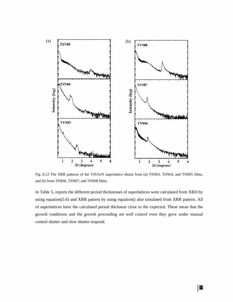
57
Fig. 8.12 The XRR patterns of the TiN/ScN superlattice obtain from (a) TSN03, TSN04, and TSN05 films,
and (b) from TSN06, TSN07, and TSN08 films.
In Table 5, reports the different period thicknesses of superlattices were calculated from XRD by
using equation(5.6) and XRR pattern by using equation() also simulated from XRR pattern. All
of superlattices have the calculated period thickness close to the expected. These mean that the
growth conditions and the growth proceeding are well control even they grew under manual
control shutter and slow shutter respond.
(b) (a)

58
Table 5 Indicate the expected period thickness (Λex) and the calculated period thickness which were determined from the θ-2θ X-ray diffraction (ΛXRD) and from the X-ray reflectivity (ΛXRR).
Film Λex
(nm)
ΛXRD
(nm)
ΛXRR
(nm)
TSN03 11.36 11.07 10.89
TSN04 5.68 5.44 5.44
TSN05 2.84 2.21 2.25*
TSN06 5.68 5.31 5.44
TSN07 5.68 5.43 5.20*
TSN08 2.84 2.73 2.67*
* It obtains from XRR simulation.
Fig. 8.13 The measured and simulated XRR patterns of (a) TSN05, (b) TSN07, and (c) TSN08. The simulation
patterns were simulated from WINGIXA program by generating TiN/ScN stacked in proper thickness to fit the
measured reflection peaks.

59
The RSM technique was using to investigate on a difference period thickness of TiN/ScN
superlattice, i.e., TSN03, TSN05 and TSN06 which are 11.62 nm, 2.64 nm, and 5.24 nm,
respectively. For example, in Fig. 8.14 show reciprocal map of TSN06 sample. The X-ray
diffraction was performed in three different regions in reciprocal space, i.e., 224, 420, and 222.
Hence, it shows TiN spot which is a seed layer (bottom electrode) and the superlattice satellite
indicated in image. This can confirms that TSN06 is superlattice. In addition, this phenomenon is
also observed in TSN03 and TSN 05 with shifted of satellite peak. The RSM of three films
shows the films are relaxed and have an in-plane lattice parameter larger than the TiN in-plane
lattice parameter (af > as).
SL0
SL+1
SL-1
SL-2
SL+3
SL-1
SL+3
TiN SL+1
SL0
SL+2 SL+2
TiN
[1 1 1]
[-1 -1 2]
(a) (b)

60
Fig. 8.14 Illustration of reciprocal space map of TSN06 sample in (a) asymmetric 2θ-ω scan at 224 map
region, (b) symmetric θ-2θ scan at 222 map region, (c) asymmetric 2θ-ω scan at 420 map with 90° sample
rotation, and (d) asymmetric 2θ-ω scan at 222 map with 90° sample rotation.
Because of this technique we can get 2D reciprocal space, the average lattice parameter in
direction that parallel substrate (a) and perpendicular to substrate (c) can be calculated from the
map. Table 4 report the average lattice parameter in different TiN/ScN superlattice samples. It
shows good agreement value in c direction between XRD and RSM result. From the map and the
average lattice parameter obtain the relaxed epitaxy relation between superlattice and TiN seed
layer. However, there is shifted in a values in 224, and 420 maps which are observed in both
sample TSN05 and TSN06. This result can be demonstrated by considering Fig. 8.14(a) and Fig.
8.14 (c). One can see that the 420 map has broadening in superlattice peak more than 224 map.
SL-1
SL0
TiN TiN SL+1
SL+3
SL+2 SL+2
SL+1
SL0
SL-1
(c)
[1 1 1]
[-2 0 2]
SL-2
(d)

61
This broadening comes from misfit of lattice parameter between layers. It generates misfit
dislocation along [-1 -1 2] direction for this case giving broadening.
Table 4 Show the average lattice spacing d and the average lattice parameter a and c of superlattice films are calculated from XRD pattern and reciprocal mapping.
Convectional θ-2θ
XRD 224 Reciprocal mapping
420 Reciprocal mapping
(90° rotation) Film
d c ||d
d⊥ a c ||d
d⊥ a c
TSN03 2.51 4.34 - - - - 1.53 1.26 4.33 4.34
TSN04 2.51 4.34 - - - - - - - -
TSN05 2.49 4.31 2.64 0.93 4.32 4.30 1.54 1.24 4.34 4.31
TSN06 2.51 4.34 2.66 0.94 4.35 4.34 1.52 1.25 4.31 4.34
TSN07 2.51 4.35 - - - - - - - -
TSN08 2.51 4.34 - - - - - - - -
Moreover, TSN07 and TSN08 were studied microstructure by TEM technique. In Fig. 8.15 and
Fig. 8.16 show ScN and TiN nanolayered multilayer structure stack along growth direction. The
period thickness of TSN07 is 5.24 nm and TSN08 is 2.67 nm, approximately which are
measured on the images. The values agree with the expected period thickness which is calculated
from the deposition rate and X-ray technique. High resolution images of both films show that the
films have an epitaxial growth on Al2O3 substrate. Fig. 8.15(d) and Fig. 8.16(d) show electron
diffraction patterns of TSN07 and TSN08. The superlattice satellite feature can be observed on
the pattern. This supports the reciprocal map observation that the TiN/ScN multilayer is
superlattice. The elertron diffraction patterns also observe that both films contain the twin
growth due to the twinning spot can be indicated in pattern.
In addition, the microstructure of both films indicates a columnar like feature or accumulate
roughness feature in the films. For TSN07, the image shows it has more columnar feature than
TSN08. In Fig. 8.16(b) obviously shows the boundary is formed when rough domain join with
flat domain or two flat domains with different period join together. This means that the
roughness evolution causes columnar feature in superlattice. The rough interface can be formed
because of the low mobility of adatom especially in nirides compound has low mobility make
adatom stick together which will form facets or small island on surface instead of layer by layer

62
growth. The small island will give a shadow effect on next incoming adatom which means the
periodicity in that region will develop and the worst case is the periodicity will be destroyed (see
Fig. 8.15(a)). On the other hand, some region that the facet is not too high film can grow on top
of facet giving a next layer will follow that feature giving a “waving” layer. In this case, the
facets are formed due to step on the substrate‡ or they can form due to facets in previous layer.
Fig. 8.15 Cross-section TEM images of TSN07 show (a) overview image, (b) magnified image at the (b)
marked area in (a), (c) the high resolution image at the (c) marked area in (a), (d) the electron diffraction
pattern of TSN07. Arrows indicate superlattice satellites
‡ It had mention in section 8.1.1.
(a)
(c)
(b)
(d)
(b) (c)

63
According to the growth condition, this condition is optimized to get a smooth TiN surface but it
is not optimized for ScN57 which explains why TSN07 has bad result in XRD compare with
TSN08, due to TSN07 have less coherent period. It also confirms the result that we had observed
in the XRR measurement.
Fig. 8.16 TEM images of TSN08 show (a) overview image, (b) magnified image at the (b) marked area in (a),
(c) the high resolution image at the (c) marked area in (a), (d) the electron diffraction pattern of TSN08.
Arrows indicate suplattice satellite.
8.1.3 Electrical properties of TiN/ScN superlattices
Electric resistivity was measured for the different TiN/ScN superlattice samples in Table 3 with
four point probe technique push against film surface that mean the parallel resistivity of the film
is established. Table 5 summaries the room temperature resistivity of TiN/ScN superlattice. For
comparison, also the resistivity of TiN, ScN and ScN on TiN bottom electrode.
(b)
(c)
(a)
(c)
(b)
(d)

64
The TiN/ScN superlattices show conduction films which has resistivity slightly higher than TiN
film. Furthermore, the TSN07 and TSN08 (without TiN bottom electrode) show higher
resistivity than films that have TiN bottom electrode. This means that the TiN bottom electrode
dominates in electrical transport of superlattice. Therefore, the four point probe technique is used
the voltage apply perpendicular to superlattice sample. This can be treated as resistors connected
in parallel (like the model shows in Fig. 8.17). Thus, the summation of resistance depends on the
lowest resistance for this case is TiN bottom layer. This model can be confirmed by we
calculated resistivity of superlattice which the resistivity close to measurement value.
Table 6 The parallel resistivity of TiN/ScN superlattice, TiN and ScN samples were obtained by four point probe technique (ρmea) and the parallel resistivity was obtained by calculate from
resistor parallel connection model is ρcal.
Films Period Film thickness
(nm)
Seed layer
(nm)
ρmea
(µΩ.m)
ρcal
(µΩ.m)
SN02 182 - 1.729
TN08 180 - 0.1951
TSN01 180 120 0.4189 0.4191
TSN02 1 and 1/2 180 120 0.3086 0.3021
TSN03 15 and 1/2 173.2 120 0.2784 0.2607
TSN04 30 and 1/2 170.6 120 0.2844 0.2587
TSN05 60 and 1/2 169.3 120 0.2890 0.2577
TSN06 30 and 1/2 170.6 120 0.3280 0.3390
TSN07 31 176.2 - 0.6691 0.3317
TSN08 60 167.3 - 0.7600 0.3318
The results were reported in Table 5 which corresponds with measurement results; however,
TSN07 and TSN08 do not consist with calculation values. It suggests that the electron filter
hypothesis by metal/semiconductor superlattice is correct or due to residue stress inside film
mismatch between expect thickness and real thickness for period.

65
Fig. 8.17 A model of superlattice resistivity measurement shows the parallel connected resistor due to the
applied voltage from four-point probe.
If we consider SN02 film, the resistivity is lower than normal semiconductor material. The SN02
film was measured chemical composition by ERDA to investigate impurity. The SN02 film has
49.4% Sc, 49.0% N, 0.8% F, 0.5% O, and 0.3 % C, respectively. The result explains that SN02
has correct stoichiometry as XRD result showed in section 8.1.1. This suggests that SN02 maybe
have the vacancies inside crystal. Hence the SN01 film was grown at 60 W (see Table. 3). It was
measured resistivity equal to 4.45 µΩ.m is 10 times higher than SN02. This gives that our
condition for growth ScN layer is not well enough.

66
8.2 Characterization of Ca-Co-O film growth by reactive sputtering
The growth conditions for Ca-Co-O films test series are reported in Table 7. Fig. 8.18 shows
XRD patterns of Ca-Co-O films grown on single crystalline Si (100) to investigate the
temperature dependence of Ca-Co-O system. The CCO01 film was grown in pure Ar gas at room
temperature. There is no peak corresponds to Ca or Co which appears in XRD pattern of a film.
This suggests that it maybe formation of amorphous of Ca/Co. For CCO02, there is one small
peak exhibits at 2θ equal at 30.72° in the pattern, it is indicated Co3O4 110. At Ts = 500 °C, the
XRD pattern of CCO03 is also show one low intensity peak at 2θ angle of 18.86° is
corresponded to Co3O4 111. CCO04 was grown at 700 °C for Ts, the diffractogram obviously
shows three peak were observed at 2θ angle at 36.27° and 42.18 which the first two peaks
exhibits films contain CoO 111 and CoO 200 phase, respectively. The last peak at 2θ angle
equals to 48.17°. This peak may correspond to the Ca3Co4O9 phase but this remains to be
confirmed.
Table 7. The growth condition of test series Ca-Co-O films. O% is a percent of oxygen flow rate in total flow rate. In this investigation, we use 73.2 and 104.3 SCCM total flow rate. Ts is the substrate temperature. Troom means room temperature.
Films PCa/Co
(W)
Ar flow
(SCCM)
O2 flow
(SCCM) O2%
Pressure
(mtorr)
TS
(°C)
Deposition time
(min)
CCO01 100 73.2 - - 3.66 Troom 75
CCO02 100 71.0 2.20 3 3.66 300 135
CCO03 100 71.0 2.20 3 3.66 500 135
CCO04 100 71.0 2.20 3 3.66 700 135
CCO05 100 98.9 5.21 5 5.39 300 135
CCO06 100 98.9 5.21 5 5.39 500 135

67
Fig. 8.18 XRD patterns of Ca-Co-O films on Si 100 substrate were varied substrate temperature (Ts), (a) at
room temperature and 3.66 mtorr in Ar with 100 W, (b) 300 °C, (c) 500 °C, (d) 700 °C. They were grown at
100 W and 3% of O2 flow in 73.2 SCCM Ar total pressure. The Si XRD peaks are indicated.
Fig. 8.19 X-ray diffractogram of Ca-Co-O films on Si 100 substrate which were grown under condition of 100
W applied voltage, 5%O2 flow in 104.2 SCCM Ar ( ≈5.39 mtorr) condition with Ts was varied (a) 300 °C and
(b) 500 °C.
In Fig. 8.19, CCO05 sample, the XRD pattern shows two peaks at 2θ angles at 30.72° and 63.87°
which can be indicated Co3O4 220 and 440, respectively. For CCO06 sample the XRD peaks
corresponding to Ca-Co-O do not appear on the XRD pattern. CCO05 is similar to CCO02
which means that sample was growth at 3% of O2 flow or 5% of O2 flow at low temperature give
the same phase in both films. However, CCO06 was grown at higher substrate temperature. It

68
does not show the XRD peaks like CCO03 which were grown at the same substrate temperature.
This suggests that the target poisoning from O2 occur during deposition, due to increasing of O2
To confirm composition of the Ca-Co-O films, EDX was used with 20 kV acceleration voltages.
Only qualitative analysis was used to analyze the data. In Fig. 8.20 show some of Ca-Co-O films
EDX spectra show that films contain Ca, Co, O and Si which are the correct composition that we
need. However, the Al impurity was discovered in all of Ca-Co-O samples. It could be explain
due to when this set of experiment performed. There is an alternate project which used the same
deposition system at that time. That project was used Al target to deposit the film when I were
started my Ca-Co-O growth, it might be a cross contamination happened during my Ca-Co-O
due to evaporation of Al which deposited on heater or Al which deposited inside chamber could
be sputtered during deposition.
Fig. 8.20 EDX spectra of (a) CCO01, (b) CCO02, (c) CCO04 and (d) CCO06 films
Considering, the absence of Ca phase in XRD peak and the intensity of Ca in EDX spectra is
quite low when they are compared. This result can explain due to Ca has quite low evaporation
temperature in our working pressure. For example, if the pressure equal to 0.1 mtorr, Ca will
have evaporation temperature approximately 565 °C58. This means that films will loss Ca content
during deposition.
(a) CCO02
(b) CCO04 (c) CCO06
(d) CCO01

69
Fig. 8.21 The cross-section SEM micrographs of (a) CCO01, (b) CCO02, and (c) CCO4 samples
The Ca-Co-O film thickness was measured by using cross-section SEM technique is show in
Table 8. In Fig. 8.21, the thickness of Ca-Co-O film can be measured. However, the images
show the thickness of Ca-Co-O films is very thin approximately 40 to 70 nm which each of them
had deposited in 2 hours. This means that the thickness is quite hard to obtain by this SEM
technique.
Table 8 The thickness of Ca-Co-O films which were measured.
Film thickness (nm)
CCO01 67.88
CCO02 46.17
CCO03 44.52
CCO04 174.43
CCO05 73.07
CCO06 -
According to the incredibly thin sample, this can describe low intensity on the XRD pattern.
Because of 100 W applied power, which took from the Al and Cr alternate project as my starting
(a) (b)
(c)

70
point give low sputtering yield§ for Ca and Co. For 4 keV Ar+-ion bombardment, the Ca has a
sputtering yield equal to ≈1 atoms/ion59 and the Co has a sputtering yield equal to ≈2.81
atoms/ion60. These are lower than the Cr has a sputtering yield at 4 keV Ar+ equal to ≈3.55
atom/ion60. From this reason show that Ca and Co has low deposition rate.
However, if one consider CCO04 sample, it is the thickest films in this set of test series. This
gives more mystery to this material, since I did not change any parameter except increasing the
substrate temperature. The deposition rate was increase rapidly compare with the rest of samples
instead of thin sample. When the substrate temperature is increase the Ca should be loss from the
film as we concluded. But comparing the EDX spectra of all samples, CCO04 has quite high
intensity of Ca which is in present contradiction.
§ sputtering yield is the number that describe how much particle can be sputtered at certain Ar+-ion energy (atoms
per ion unit)

71
9 Conclusion
“Imagination is more important than knowledge”
Albert Einstein
From, the issues of this thesis that I had propose in first chapter.
• First, growth and characterization of thermoelectric multilayeres or superlattices which is
an artificial nanolaminate of TiN/ScN by using reactive DC magnetron sputtering on
Al2O3 (0001).
• Second, the thermoelectric cobaltate, I would investigate in growth and characterize of
[Ca2CoO3]xCoO2 on Si (001) by using reactive RF magnetron sputtering.
First part of investigation, we tried to grow the TiN/ScN superlattice for thermoelectric materials
application by reactive DC magnetron sputtering with manual control shutter. To capable for in-
plane and out-of-plane resistivity measurement, the TiN/ScN superlattices were grown on TiN
bottom electrode. During investigation the result shows highly influence of substrate surface to
obtain smooth TiN bottom electrode. This brought to a high attentive thinking in topography of
substrate surface and cleaning process. In term of structure of superlattice, the XRD, XRR, and
RSM results confirm that we get TiN/ScN superlattice according to superlattice satellite appare
on the diffractogram. We also observed the period thickness of superlattices followed the growth
condition. In addition, the RSM shows the overall of superlattices are relaxed.
According to cross-section TEM microscopy, it shows that the roughness evolution occur in
superlattices due to a limiting in mobility cause by defect on substrate surface. The results also
support that if we start by smooth surface, we will obtain better quality superlattice, since this
thesis we had only optimized for smooth TiN. This concludes that we have to optimize in both
film to get better quality. In the electron diffraction pattern, it shows we get a single crystal
superlattice and also superlattice satellite which a twin structures appear. In electronic properties,
TiN/ScN superlattices were measured resistivity by four point probe technique. The entire of test

72
series superlattice exhibits resistivity in metallic. The results suggest that the resistivity of
superlattice is influenced by TiN bottom electrode. In the film without bottom electrode show the
resistivity slightly increase. It maybe come from off stoichiometry ScN due to it has vacancies
which give it has low resistivity.
Secord, I tried to growth [Ca2CoO3]xCoO2 by reactive RF magnetron sputtering. The XRD
results exhibit very low intensity on pattern. Films were grown at same condition and the
substrate temperature was varied 300 °C and 500 °C show Co3O4 phase and absent in
[Ca2CoO3]xCoO2 phase. The film grew at 700 °C, the XRD pattern shows CoO phase appear
with unknown phase which I expect that it might be [Ca2CoO3]xCoO2, however, due to poor
database I cannot certain that it is a [Ca2CoO3]xCoO2. For O2 flow influence, a film was grown
under 5% O2 flow in 104.2 total pressure at Ts = 300 °C which the XRD pattern shows similar
result with the film was grow at lower O2 flow under the same condition of the rest parameter.
And then at Ts = 500 °C, there is no peak appear in the pattern.
From the cross-section SEM show the Ca-Co-O films had incredible thin. This can explain by
the growth condition give the system operates in oxide mode which has low deposition rate due
to target poisoning. This effect maybe dominates by low sputtering yield. In EDX spectra, they
show my films had Al contaminate according to cross contamination from my colleague project.
According to Ca has low evaporation temperature, this is showed in the XRD that there is no
peak that correspond to Ca phase. Also the low Ca intensity in EDX spectra which is compared
between spectra maybe suggest that the Ca content is lost by evaporate during deposition.
However, this thesis discovered a big contradiction when we observed the Ca-Co-O film was
grown at 700 °C, it shows slightly high intensity in XRD pattern compare with the rest of films.
It exhibit thick film instead of thin as we observe in the other film. Also, it has high Ca intensity
in EDX spectra when it is compared. This gives mystery to this kind of material which needs to
have more study.

73
10 Future work
This thesis is the result of my Master’s project and it has a limited of time in advance. There are
some idea and question which have not the answer and come up during project work. Some of
those idea and question are listed below.
• The TiN/ScN superlattice need to be grown in a better way such as the automatically fast
shutter control, the capable substrate temperature heating at 800 °C, etc.
• Of course, this work is related with thermoelectric materials The TiN/ScN superlattice
need to measure the thermoelectric parameter (Seebeck coefficient, electrical
conductivity, thermal conductivity).
• From above, I will try to play around with different individual material thickness how it
effect to thermoelectric parameter. Due to the electron filter idea.
• There is no study about thermal stability of the metal-seimconductor superlattice for
thermoelectric materials that work above room temperature. It would be better to study
such that thing.
• According to the same idea, I try to use different materials to make a superlattice.
Especially, the semi-metal group (like rare-earth nitride such as GdN, YN, etc) due to the
charge carrier maybe in a range that give good contribution in the transport phenomena.
Also, all of those materials have magnetic behavior which means that maybe the
magnetocaloric effect can be enchanted the cooling effect.
• Primary continuing study of Ca-Co-O system uses TEM to determine crystal structure
and confirm phase of films that obtain from XRD.
• In Ca-Co-O materials system, they need to study more about the growth to understand
their behavior. This will lead us to know what and how it contributes to give
[Ca2CoO3]xCoO2 materials be a good thermoelectric material.
• I also interest to grow [Ca2CoO3]xCoO2 by reactive co-sputtering from individual Ca and
Co target to give opportunity to alloy Ca with another materials.

74
References
1http://www.grida.no/publications/vg/climate/ (21 February 2010). 2F. J. DiSalvo, Science 285, 703 (1999). 3K. Matsubara and M. Matsuura, in CRC Thermoelectrics Handbook Macro to Nano, edited by
D. M. Rowe (CRC, Boca Raton, 2006), p. 1-10. 4S. B. Riffat and X. Ma, Appl. Therm. Eng. 23, 913-935 (2003). 5G. A. Slack, in CRC Handbook of Thermoelectrics, edited by D. M. Rowe (CRC, Boca Raton,
1995). 6H. J. Goldsmid, Introduction to Thermoelectricity (Springer, Heidelberg, 2009). 7C. B. P. Finn, THERMAL PHYSICS, 2 ed. (Chapmam & Hall, London, 1993). 8G. S. Nolas, J. Shaph, and H. J. Goldsmid, Thermoelectrics: Basic Principles and New
Materials Developments (Spinger, Heidelberg, 2001). 9D. M. Rowe, in CRC Thermoelectrics Handbook Macro to Nano, edited by D. M. Rowe (CRC,
Boca Raton, 2006), p. 1-10. 10H. J. Goldsmid, in CRC Handbook of thermoelectrics, edited by D. M. Rowe (CRC, Boca
Raton, 1995). 11D. M. Rowe, in CRC Thermoelectrics Handbook Macro to Nano, edited by D. M. Rowe (CRC,
Boca Raton, 2005), p. 1-10. 12D. M. Rowe, CRC Handbook of Thermoelectrics (CRC, Boca Raton, 1995). 13G. J. Snyder and E. S. Toberer, Nat. Mater. 7, 105-114 (2008). 14H. J. Goldsmid and R. W. Douglas, Br. J. Appl. Phys. 5, 386-390 (1954). 15H. J. Goldsmid, A. R. Sheard, and D. A. Wright, Br. J. Appl. Phys. 9, 365-370 (1958). 16E. A. Skrabek and D. S. Trimmer, in CRC Handbook of thermoelectrics, edited by D. M. Rowe
(CRC, Boco Raton, 1995). 17J. R. Salvador, J. Yang, X. Shi, H. Wang, and A. A. Wereszczak, Journal of Solid State
Chemistry 182, 2088-2095 (2009). 18B. A. Cook, M. J. Kramer, X. Wei, J. L. Harringa, and E. M. Levin, J. Appl. Phys. 101, 053715
(2007). 19G. S. Nolas, J. L. Cohn, and G. A. Slack, Phys. Rev. B 58, 164-170 (1998). 20T. M. Tritt, G. S. Nolas, G. A. Slack, A. C. Ehrlich, D. J. Gillespie, and J. L. Cohn, J. Appl.
Phys. 79, 8412-8418 (1996).

75
21Y. Xia, S. Bhattacharya, V. Ponnambalam, A. L. Pope, S. J. Poon, and T. M. Tritt, J. Appl.
Phys. 88, 1952-1955 (2000). 22M. Christensen, A. B. Abrahamsen, N. B. Christensen, F. Juranyi, N. H. Andersen, K.
Lefmann, J. Andreasson, C. R. H. Bahl, and B. B. Iversen, Nat. Mater. 7, 811 (2008). 23F. D. Rosi, Solid-State. Electron. 11, 833-863 (1968). 24L. D. Hicks and M. S. Dresselhaus, Phys. Rev. B 47, 12727-12731 (1993). 25G. D. Mahan and J. O. Sofo, Proc. Nat. Acad. Sci. USA 93, 4436-7439 (1996). 26D. G. Cahill, W. K. Ford, K. E. Goodson, G. D. Mahan, A. Majumdar, H. J. Maris, R. Merlin,
and S. R. Phillpot, J. Appl. Phys. 93, 793-817 (2003). 27R. Venkatasubramanian, E. Siivola, T. Colpitts, and B. O'Quinn, Nature 413, 597-602 (2001). 28D. Vashaee and A. Shakouri, Phys. Rev. Lett. 92, 106103 (2004). 29J. M. O. Zide, D. Vashaee, Z. X. Bian, G. Zeng, J. E. Bowers, A. Shakouri, and A. C. Gossard,
Phys. Rev. B 74, 205335 (2006). 30D. Vashaee and A. Shakouri, J. Appl. Phys. 95, 1233-1245 (2004). 31M. Zebarjadi, Z. Bian, R. Singh, A. Shakouri, R. Wortman, V. Rawat, and T. Sands, J.
Electron. Mater. 38, 960-963 (2009). 32V. Rawat, Y. K. Koh, D. G. Cahill, and T. D. Sands, J. Appl. Phys. 105, 024909 (2009). 33D. Gall, I. Petrov, L. D. Madsen, J.-E. Sundgren, and J. E. Greene, J. Vac. Sci. Technol. A 16,
2411-2417 (1998). 34D. Gall, I. Petrov, and J. E. Greene, J. Appl. Phys. 89, 401 (2001). 35C. Stampfl, W. Mannstadt, R. Asahi, and A. J. Freeman, Phys. Rev. B 63, 155106 (2001). 36C. Höglund, J. Bareño, J. Birch, B. Alling, Z. Czigány, and L. Hultman, J. Appl. Phys. 105,
113517 (2009). 37K. Lal, A. K. Meikap, S. K. Chattopadhyay, S. K. Chatterjee, M. Ghosh, K. Baba, and R.
Hatada, Physica B 307, 150-157 (2001). 38I. Terasaki, Y. Sasago, and K. Uchinokura, Phys. Rev. B 56, R12685-R12687 (1997). 39K. Sugiura, H. Ohta, and K. Koumoto, Int. J. Appl. Ceram. Technol 4, 308-317 (2007). 40A. Weidenkaff, R. Robert, M. Aguirre, L. Bocher, T. Lippert, and S. Canulescu, Renew. Energ.
33, 342-347 (2008). 41G. Xu, R. Funahashi, M. Shikano, I. Matsubara, and Y. Zhou, J. Appl. Phys. 91, 4344-4347
(2000). 42B. C. Sales, Int. J. Appl. Ceram. Technol 4, 291-296 (2007). 43Y. F. Hu, W. D. Si, E. Sutter, and Q. Li, Appl. Phys. Lett. 86, 082103 (2005).

76
44H. Minami, K. Itaka, H. Kawaji, Q. J. Wang, H. Koinuma, and M. Lippmaa, Appl. Surf. Sci.
197-198, 442-447 (2002). 45A. Sakai, T. Kanno, S. Yotsuhashi, A. Odagawa, and H. Adachi, Jpn. J. Appl. Phys. 44, L966-
L969 (2005). 46A. C. Masset, C. Michel, A. Maignan, M. Hervieu, O. Toulemonde, F. Studer, B. Raveau, and
J. Hejmanek, Phys. Rev. B 62, 166-175 (2000). 47J. Birch, "Single-crystal Mo/V superlattices; growth, structure, and hydrogen uptake", Ph. D.
Thesis, Thin Film Physics, Department of Physics and Measurement Technology, Linköping
University, Sweden, 1997. 48T. Takada and T. Shinjo, Metallic superlattices (Elsevier, Amsterdam, 1987). 49Y. Fujii, in Metallic superlattices, edited by T. Shinjo and T. Takada (Elsevier, Amsterdam,
1987). 50P. Eklund, M. Beckers, U. Jansson, H. Högberg, and L. Hultman, Thin Solid Films 518, 1851
(2010). 51M. Ohring, The materials science of Thin Films, 2 ed. (Academic Press, California). 52P. E. J. Flewitt and R. K. Wild, Physical Methods for Materials Characterization, 2 ed.
(Institute of Physics Publishing, Philadelphia, 2003). 53M. Birkholz, Thin Film Analysis by X-Ray Scattering (WILEY-VCH, Weinheim, 2006). 54J. Birch, "Single-crystal Mo/V superlattices; growth, structure, and hydrogen uptake", Ph. D.
Thesis, Thin Film Physics, Department of Physics and Measurement Technology, Linköping
University, Sweden, 1994. 55V. E. Henrich and P. A. Cox, The Surface Science of Metal Oxides (Cambridge University
Press, Cambridge, 1994). 56N. Ghafoor, "Materials Science of Multilayer X-Ray Mirrors ", Ph.D Thesis, Thin Film
Physics, Department of Physics, Chemistry and Biology (IFM), Linköping University, Sweden,
2008. 57J. Birch, T. Joelsson, F. Eriksson, N. Ghafoor, and L. Hultman, Thin solid films 514, 10-19
(2006). 58R. E. Honing and D. A. Kramer, RCA review 30, 285-303 (1969). 59C. S. Hansen, W. F. Calaway, B. V. King, and M. J. Pellin, Surface Science 398, 211-220
(1998). 60N. Matsunami, Y. Yamamura, Y. Itikawa, N. Itoh, Y. Kazumata, S. Miyagawa, K. Morita, R.
Shimizu, and H. Tawara, At. Data Nucl. Data table 31, 1 (1984).

77