nanocomputers and swarm intelligence || elements of technology for information systems of the new...
TRANSCRIPT

Chapter 5
Elements of Technology for Information Systems of the New Century
5.1. Beyond processors
Restricting future trends and the next generation’s computers by focusing only on the processor would be over simplistic. Apart from the race towards higher performance and the miniaturization of circuits, the progress of information systems takes place principally in the production of computer memory and mass storage. However, even this “turgescent” vision does not sufficiently characterize the development of computers over the next two decades.
Since the computer has become portable and a tool for communication, it has been integrating itself into our world in an ever more natural and comprehensive way. The schematic or, in other words, simplified structure of a computer can currently be divided into the following five blocks: the processor, memory and mass storage, telecommunication networks which allow the interaction with other machines, power supplies which now predominantly allow mobility and web diffusion and, last but not least, the interface between the user and the machine or the machine and its environment.
Imagining the computer of the future requires imagining a joint development of these five elements of technology as they often have a strong impact on each other.
Nanocomputers and Swarm Intelligence Jean-B aptiste Waldner
Copyright 0 2008, ISTE Ltd.

136 Nanocomputers and Swarm Intelligence
As previously done for processors, all technologies need to be sub-divided into their current industrial applications and their long term perspectives out of which some may always remain in the area of exploratory research. The combination of different available solutions leads to a chronological outlook on the development of computers and information systems over the next 15 years.
Figure 5.1. The roadmap of information systems over the next two decades
The roadmap of the information systems for the next two decades is based on five dimensions:
– smaller, faster and more powerful processors which use traditional silicon technology but remain open to new developments. These new developments may find complex applications by leading companies into the fields of payment mandates, cryptography, expert systems, etc. Current applications will then become technologies of the past;

Elements of Technology for Information Systems 137
– memory which mainly aims for the smallest possible number of electrons needed to store one bit. Currently, several hundred thousand electrons are “discharged” in the process of storing one single bit. The ultimate goal is the development of memory that consists of only one electron and is also non-volatile, in other words, it does not need a periodic refresh rate to maintain the information saved. New technologies will therefore progressively reduce the number of electrons used, increase the speed of transferring data and decrease the electricity consumption. In the field of mass storage, the density of the information stored will play a predominant role as today all information is stored on digital devices. Research is mainly concentrated on three-dimensional storage which saves information as an entire “page” during each transfer. It should be kept in mind that current storage devices are two-dimensional, which means that the information is cut into small chunks and applied to the surface of a magnetic or optical disk, as was the case for magnetic tapes and punched cards. These new solutions take their inspiration from the living world: information is stored in the three dimensions of a protein. Similarly, in the field of optics, data is stored in a three-dimensional hologram in the center of an extremely small crystal;
– the third axis of progress is that of power supply, which has become crucial since systems have become more and more portable. The race towards the independence of power supplies and the importance of weight began with the appearance of laptops, cell phones, PDAs and other digital portable devices. However, with the notion of web diffusion the problem has increased. Currently, “intelligent” devices are extremely small and often permanently integrated into their environment (e.g. biochips and microsystems), so that replacing a power supply would be very complex and therefore virtually impossible. These new power supplies will perpetuate progress in the field of electrochemical batteries (e.g. lithium polymer batteries which are extremely slim, zinc-air batteries in which particles of zinc are mixed with an electrolyte). Furthermore, they allow for a density of energy which is 100 times higher than that of traditional batteries. In other words, their lifespan is just as long as the device’s lifespan. These power supplies cannot exceed the dimension of the sub-millimeter and need to be rechargeable while working, for example, the on-going production of energy through mechanical vibrations;
– the fourth axis of development concerns the interfaces with the user or the environment interfaces. From a simple keyboard and screen, the computer has developed in around 40 years into something that understands all five human senses and nearly all natural movements. The application of speech recognition on a large scale is now just as common as handwriting recognition. The impressive progress in these fields will allow for smoother, faster and more natural exchanges with machines. Information will be always shown on some form of screen. Current screens using LCD or plasma technology, as new as they may be, will soon be overtaken by less energy consuming technologies. Screens will also be even flatter.

138 Nanocomputers and Swarm Intelligence
The use of a backlight will end and be replaced by ambient light with a better use of the light in the surrounding area. These screens can modify their shape and can be folded just like a piece of paper. In the long term, there is also the possibility of creating an interface that senses and gestures. This interface which directly connects the brain and the machine introduces the notion of telepathic control. For a long time these applications were thought of as a device which would be implanted into our body and would therefore require an operation. Their application was perceived as ethically unacceptable. However, new and very promising applications which will not be implanted into our body have been developed and could enter the market in about 5 to 10 years’ time;
– the fifth axis of development is that of the communication between systems, in other words, networks and telecommunications. If the Internet mainly consists of the global interlinking of traditional networks, the next step, which will favor the development of ambient intelligence and web diffusion, is being developed on the level of large-scale wireless networks. The specialty of these new networks lies in the fact they no longer require permanently installed antennae. These networks consist of active nodes or, in other words, antennae which are directly integrated in the terminals (i.e. the objects that interact with each other). These telecommunication systems will be able to manage themselves. This analog principle known as P2P (see section 4.3.3) is perfectly adapted to the introduction of a highly interlinked network of objects that constantly interact with each other.
5.2. Memory and information storage systems
In the development of digital appliances, one very important factor is the incredible increase in the memory required to execute commands as well as to save data on a permanent basis. Multimedia files which are becoming increasingly large in terms of memory (sound, photos, videos, etc.) are largely responsible for the constant need to increase computer storage capacity. Future generations of machines will accommodate this tendency in the fields of RAM and mass storage.
The technology of magnetic data storage will have followed the same development as the semi-conductor. The speed of computers and the density of data storage has increased one hundredfold between 1985 and 1995. The same factor was also observed between 1995 and 2005. However, in the field of silicon we are about to come up against a “memory wall” in the development of magnetic storage of data. In other words, in the short term current technology will have brought the density of information storage to its maximum capacity. This limit is super-paramagnetic, which means that the binary data stored are positioned so close to one another that their magnetic polarities start interfering with each other. An even denser storage of data would mean that non-magnetic technology would need to be applied. The

Elements of Technology for Information Systems 139
research, whose results are most likely to enter the market in the near future, relies on holographic memories or the usage of devices which derive from the use of atomic force microscopes (AFM) for mass storage.
Furthermore, memory in current computers relies on the globally applied technology of semi-conductors which was mentioned above. It is subject to the same physical limits as processors and might also be replaced by other solutions. Increasing the performance of computer memory requires a reduction in the number of electrons needed to store a single bit of information. From the very beginning of information technology the objective of minimizing the electrons used for the procedure of storing on a single bit has been the decisive factor in the development of storage devices. Today, several thousand million electrons are required to store one piece of binary information. The ultimate goal would be that only a single electron is used. Other approaches simply spare themselves the trouble of working with electrons. They exploit the properties of photosensitive materials such as three-dimensional organic memories (see section 3.6.3).
In 1997, the largest database was Knight Ridder’s DIALOG with a capacity of seven terabytes (according to www.SearchDatabase.com).
In 2002 the largest database was that of the Stanford Linear Accelerator Center which allowed for the storage of more than 500 terabytes of experimental data, which was close to 5% of that year’s global storage capacity.
Techniques of parallel processing as well as optical interconnections help to resolve the limited speed of data transfer in computers that could easily adopt hybrid technologies.
Figure 5.2. The market of mass storage (source IDC – 2003)

140 Nanocomputers and Swarm Intelligence
5.2.1. Memories consisting of semi-conductors – perspectives
RAM or today more precisely DRAM (Dynamic RAM) is a space that allows the temporary storage of data while the program is running, as opposed to storing it on a mass storage memory such as the hard disk. DRAM needs to be “refreshed” periodically to preserve the stored data. This is why it is called dynamic. Once the computer is switched off all data saved in this memory is erased.
A DRAM memory unit consists of a MOS transistor and a capacitor. Once the transistor is activated it becomes permeable and charges the capacitor. DRAM cells are situated on a lattice and at the intersections of lines and columns. It is therefore possible to either “read” the tension of the capacitor or “write” the logic value by creating a difference in the potential of the capacitor’s terminals (e.g. +5 V or 0 V according to the value to be written).
The capacitor discharges at some point because of leaks in the electric current. This is why the work cycle of the memory includes a refresh period of the data which consists of reading and simultaneously rewriting the logic state of all points to be saved in one row.
SDRAM (Synchronous Dynamic Random Access Memory) is the next generation to follow DRAM. This type of memory synchronizes the entry and exit of signals at the rate of the control bus of the processor in order to optimize efficiency. SDRAM, which appeared in 1996, is now hardly used. It has been replaced by the DDR RAM (Double Data Rate RAM) which is synchronized twice during the work cycle, rising and falling at the front during each clocked work cycle. DDR RAM is therefore twice as fast as the SDRAM.

Elements of Technology for Information Systems 141
Figure 5.3. DDR2 is the next step in development and doubles the performance of DDR RAM. Being faster, it also offers a higher capacity because if the current DDR circuits are limited to
1 Gbit, DDR2 allows for the capacity of 2 Gbits or 4 Gbits. With the increased frequency, memory cells in the DDR start to suffer from 200 MHz onwards. The frequency will be
brought down to 100 MHz while maintaining the performance. This means that the frequency of the I/O buffer is doubled at the same time. The DDR2 rate of 100 MHz for the cells lets these deliver 4 bits per work cycle to the I/O buffer which works at a rate of 200 MHz. The bandwidth of a DDR2 at the rate of 100 MHz is therefore the double of a DDR at a rate of
200 MHz. The output based on a rate of 100 MHz is therefore ((100*4)*64)/8 = 3,200 Mo/s
A RAM produced in 2005 consists of a chip of 4 Gbits (512 Mo) engraved on 0.10 micron. The new generation of circuits allows for the reduction of the price per unit (i.e. price per bit) by more than 60% in comparison to the chips of 128 Mbits. They allow an output of more than 10 gigabytes/s. The generation of DDR3 should bring about a bandwidth of more than 16 gigabytes/s.
In order to “write” a single bit of data into a new memory cell of the RAM, a transistor transfers around half a million electrons to a neighboring capacity. This minimal quantity of charge carriers is necessary to ensure the reliability of the saved information, i.e. to preserve the data and make it detectable in the field of ambient electric noise.

142 Nanocomputers and Swarm Intelligence
Figure 5.4a. A DRAM stores a bit of information in the form of an electrical charge. It uses the capacity of certain semi-conductors (capacity of a wired grid of the MOS transistor)
Figure 5.4b. SRAM (static RAM) works differently from DRAM. Its content does not need to be refreshed periodically. One advantage of this kind of memory is its speed. On the other hand, it is much more expensive than DRAM and takes up four times more space than the
latter given its limited density of integrating data: SRAM consists of a flip-flop. Every flip-flop consists of six transistors. The information remains saved as long as there is a different
potential between the different terminals of the cell. This form of RAM also needs a permanent form of power supply. However, it uses an extremely low current of electricity which could be supplied by a small battery. DRAM, on the other hand, stores an electric
charge in the capacitor which is affected by leaks and needs a refresh period, consuming higher amounts of energy

Elements of Technology for Information Systems 143
The highest density in information storage is subject to the size of its capacities or very small capacitors whose dimensions are proportional to the quantity of charge carriers needed to save the data. A device which works by using less electrons to save a piece of information would therefore be even smaller and would consume even less energy.
With current technology, electrons are used each time information is “written” and therefore saved somewhere. The faster a computer is in these writing processes, the more energy it consumes. These are therefore not very compatible with today’s equipment which is becoming more and more portable and therefore restrains the amount of energy that can be used. Furthermore, traditional DRAMs do not limit energy consumption to the process of “writing” a piece of information. In order to save a piece of information, an electric current needs to be injected into the circuit on a permanent basis. If the power supply fails, the information is lost.
The concept of a non-volatile RAM is the main objective for researchers in this domain. A single-electron memory is the ultimate aim of this technology. It would allow for an extremely high density of integration, a much faster access (less charge carriers lead to less inertia) and a very low energy consumption. In 1999 Hitachi announced the creation of a technology which was able to create memory chips of 8 Go with an access time of 10 nanoseconds. An example of this would be all of the sound effects of a film which could, in this case, be stored one a single chip. Since this technology is able to save the data when the computer is switched off, it could be a replacement for the hard disk.
This technology is called PLEDM (Phase-state Low Electron-number Drive Memory). It only uses 1,000 electrons to store one elementary bit, which is 500 times less than traditional DRAM as the information is not stored in a capacitor but in the gate of another transistor, in other words, an amplification cell which introduces a transistor at a low electric noise so the signal of 1,000 electrons is reinforced.
The amplification transistor is installed underneath the storage transistor. Both are installed in the same cell in order to integrate this circuit on an even higher level. The storage transistor uses an electronic shutter which closes the transistor in the case of a power supply failure so the electrons remain inside the cell. In fact, this new generation of RAM could combine the advantages of the currently used DRAM (high density of integration) and SRAM (non-volatile) in order to improve the performance of both technologies. Functioning in the same time as a RAM and as a miniaturized mass storage, this would have a major impact on the most significant domains in the digital world such as portable devices, telephones, audio/video players and recorders as well as PDAs, etc.

144 Nanocomputers and Swarm Intelligence
This technology is the starting point of the transition process towards a single-electron memory in which the presence or absence of a single electron in an atom would allow a single binary information to be saved. This miniaturization of memory cells will certainly take a different route from traditional transistors. In 2006, researchers working for IBM in Zurich managed to trigger a reaction of an organic molecule which was smaller than 1.5 nm (100 times smaller than current transistors) with an electric stimulation and therefore store and retrieve binary information from it. This synthetic molecule called BPDN-DT preserved its capacity of functioning as a capacitor over several hours and after more than 500 tests. This is currently a remarkable result for a monomolecular system.
The exact process of communication with this molecule still needs to be analyzed in great depth. The extremely high speed of communication, however, is already certain. Current tests revealed that the device reacts in less than 640 ms. The outer limits of this speed have not yet been established, which could theoretically allow for the production of memories that work at more than 1,000 GHz!
Figure 5.5. The experimental circuit switching of an BPDN-DT molecule. The synthetic molecule is placed between two electrodes and under a Scanning Electron Microscope
(SEM)1. These electrodes function as an extension which will eventually break down the reversible “nano-bridge” which forms the molecule that communicated with the circuit. This
method is called mechanically controllable break junction (MCBJ). The electrodes are adjusted to a tolerance in the spectrum of the pictometer (10-12 m). In these dimensions, the
Joule effect is a major obstacle in the experiment (source IBM)
1 Scanning Electron Microscopy (SEM) is based on the principle of interactions between electrons and matter. A beam of electrons is shot towards the surface of the sample which in response sets certain particles free.

Elements of Technology for Information Systems 145
Another approach to future memory exists using semi-conductors. This approach does not use an electric charge to store information, but a magnetic field, or more precisely the phenomenon of spintronics observed in the individual components. It is called the tunnel magnetoresistance effect. This device is known as MRAM (Magneto-resistive Random Access Memory). This type of memory consists of a magnetic tunnel junction with a giant tunnel magnetoresistance effect (see section 5.2.2). It is associated with the majority of the advantages of memory based on semi-conductors currently available on the market, such as high speed when storing and reading data, a low energy consumption and being non-volatile. Because of its increased degree of integration (small sized cells and the possible reduction of the homothetic size) and its infinite cyclability2, it has been the successor of flash memory which is rather slow in the writing process and has a high energy consumption. Its imperviousness to radiation, to name just one of the DRAM’s qualities, will, in the medium term, lead to its application in the military domain as well as space travel.
IBM and Infineon were the forerunners of this new technology. Sony, Philips, Motorola, Toshiba and NEC have joined them as well. The first applications on a wide scale concern the generation of cell phones from 2006 onwards. This market could represent $2 billion up to 2008. By 2012, it is estimated to reach $12 billion.
Figure 5.6. The tunnel effect is designed to fit the quantum object’s properties and may break the barrier of the potential. According to traditional mechanics, such a breakthrough is impossible: a magnetic tunnel junction (MTJ) consists of two ironmagnetic layers with
different magnetic polarization which are separated by a fine layer of isolation. Electrons which are injected perpendicularly into the MTJ are polarized on their way by magnetic
electrodes and permeate the isolating barrier with the tunnel effect. This tunnel transmission depends on the relative magnetization of the two electrodes to the interfaces with the tunnel barrier and the type of barrier. The resistance of such a junction can therefore take on two
extreme states; one for a parallel configuration and the other for an orthogonal configuration: this phenomenon is known as tunnel magnetoresistance (TMR)
2 The cyclability gives the possible number of writing and reading cycles, which characterizes the lifespan of a storage device.

146 Nanocomputers and Swarm Intelligence
In a “standard” layout of MRAM, the activation of the parts responsible for the writing of information is carried out with the help of minuscule magnetic fields induced by a lattice of semi-conductors which are subject to electric impulses.
Only the part in the memory which is situated at an intersection of two lines of selected current (i.e. lines/columns) turns around (the spin is inversed).
During the reading process, a low current is sent by a CMOS transistor to read the resistance of the junction. This layout brings certain limits with it. These are, for example, errors concerning the activation and the distribution of fields destined to inverse the spin in the memory’s lattice, the limitation of the ultimate density due to three different levels of lines which move the transistor to the desired point within the memory and, last but not least, the high energy consumption.
5.2.2. Limits of magnetic data storage
More than five million terabytes3 are stored each year on mass storage devices. This includes hard disks, optical devices such as CDs and DVDs and other magneto-optical devices. Magnetic hard disks make up two thirds of the entire market of storage devices. These storage devices need a few milliseconds to access the information and are much slower than RAM. The surface which is occupied by a bit of information on a disk has been reduced by a factor of 100,000 in the last 30 years. The capacities of data storage and the time needed to access them have improved and led to a drop in the prices of storage systems.
“In the future we will ask ourselves about the era when man had libraries in which the books did not talk to each other.”
(Marvin Minsky)
3 The USA alone produces 40% of all new information that is stored. This is one-third of the worldwide amount of information produced by the press and the film industry. The USA creates 40% of all information stored on optical devices and 50% of all information stored on magnetic devices.
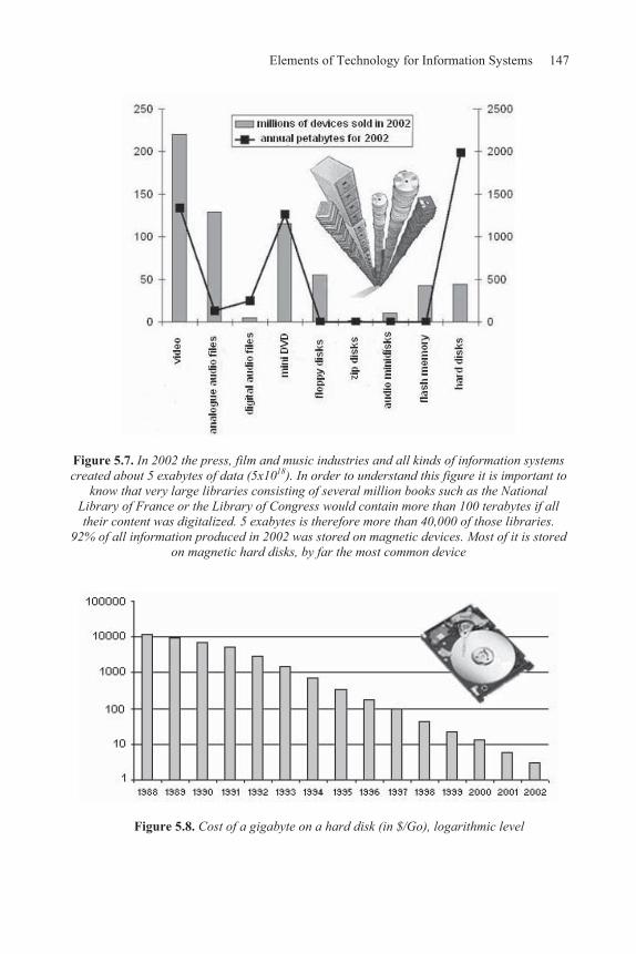
Elements of Technology for Information Systems 147
Figure 5.7. In 2002 the press, film and music industries and all kinds of information systems created about 5 exabytes of data (5x10¹⁸). In order to understand this figure it is important to
know that very large libraries consisting of several million books such as the National Library of France or the Library of Congress would contain more than 100 terabytes if all their content was digitalized. 5 exabytes is therefore more than 40,000 of those libraries.
92% of all information produced in 2002 was stored on magnetic devices. Most of it is stored on magnetic hard disks, by far the most common device
Figure 5.8. Cost of a gigabyte on a hard disk (in $/Go), logarithmic level

148 Nanocomputers and Swarm Intelligence
The race towards a higher memory capacity and speed of accessing the data is taking place in an incredible manner. The density of storage is increased by reducing the size of the magnetic mark left on the disk. This means that in order to increase the density, the size of the disk’s read/write head needs to be reduced but its sensitivity needs to be increased. These improvements depend very much on the materials used.
A density of storage higher than 80 Gbits/in² can today be applied with the exploitation of GMR, which was mentioned in the previous chapter. GMR is a phenomenon that very rapidly decreases the resistance of certain materials when a magnetic field is applied to them. This phenomenon is referred to as “giant” since never before has such an effect been observed in the field of metals. The GMR phenomenon became very interesting for industrial and commercial ventures as it detects a very small magnetic field due to an altering electric current.
GMR disk read/write heads appeared on the market in 1997. Most modern computers are currently equipped with them. A GMR disk read/write head can in its structure be compared to magnetoresistive heads, which were used in previous generations of disks. The principle is based on detecting induced electric current through a coil which is subject to an electric field. MR heads consist of a receiver made up of NiFe in which the resistance changes according to the magnetic field which can be found on the surface of the hard disk. In the case of GMR heads, the writing process is always carried out by an inductive head. The reading process, however, relies on the quantum properties of an electron with two possible spins. When this spin runs parallel to the orientation of the magnetic field of the hard disk a weak resistance can be observed. If the spin, however, takes place in the opposite direction a strong resistance can be observed.
Changes in MR heads affect the electric resistance of an element placed near a magnetic field. However, GMR heads use extremely fine layers of material, so the reading and writing process is much more exact than the one given by MR heads. This is why they are described as “giant”. As the device is much more sensitive and much smaller, magnetic traces on the disk can be detected. Due to this increased sensitivity of the GMR heads, very small fields can be detected and smaller bits can be written. The density of information stored on one disk can therefore be increased. Since GMR heads entered the market in 1997, the density of storage increased a hundredfold.

Elements of Technology for Information Systems 149
The concept of a magnetic hard disk originated in the 1950s. IBM’s engineers discovered that the read/write heads, if they were constructed appropriately, could work from underneath the surface of the rotating disk and read the data without establishing direct contact with the disk’s surface.
The first hard disk produced by IBM was called RAMAC (Random Access Method of Accounting and Control) and introduced in 1956. The device weighed nearly one ton and had a capacity of about 5 megabytes (2 Kbits/in²) as well as a transfer rate of 8.8 Ko/s.
In 1973, IBM presented the 3340, the predecessor of the modern hard disk, which for the first time was based on a sealed environment. Each unit consisted of separate modules, one stable and one movable, and each of them had a capacity of 30 Mo. This is why the disk was often called “30-30”. Referring to the Winchester 30-30 gun, this hard disk is nicknamed the Winchester hard disk.
At present, we are reaching the limits of “traditional” GMR heads, i.e. GMR heads with the electric current running parallel to the layers. The next generation of disks will use other effects of spintronics such as TMR (see section 5.2.1) or GMR with a current that runs perpendicular to the layers.
Another approach to increase the density of storage uses a vertical orientation of the disk’s magnetic dots so that they are perpendicular to the surface of the disk rather than “lying flat” towards the read/write heads. If the size of a magnetic dot decreases, the magnetic field also decreases more quickly. This phenomenon is known as auto-depolarization. A periodic refreshment of the content is required more frequently.
However, all these incremental improvements in storage devices share the same fate as expressed in Moore’s Law. They will “hit a wall” which will manifest itself as an asymptote of their performances. If the density of storage on disks reaches a three-digit growth rate, this could not be more than 100 Gbits/in² (the very next generation). A development which exceeds these dimensions will require new technology.
Saving data with an ultra high density could be an alternative to the present system which is based on a different approach. Information would no longer be written on a medium such as the currently used hard disks, but on a magnetic contact of a length of several dozen nanometers. In this case, the density of storage could reach 200 Gbits/in² instead of today’s 80 Gbits/in². Optimists imagine that this approach would allow the limits of magnetic storage to be pushed even further towards dimensions of TeraBits/in².
150 Nanocomputers and Swarm Intelligence
In portable equipment, miniaturization is the essence for future generations of digital ubiquity. An increasing number of experts consider the relatively fragile hard disk, in terms of miniaturization and the fact that it is a rotating mechanical system, which is far from being ideal, even in the short term. Samsung, amongst others, drew its conclusions from this fact: solid state disks (SSD) replaced the traditional hard disk drive (HDD) with a flash memory. The Korean producer wanted to take over 20% of the storage market by 2008 with this technology, producing hundreds of millions of them. According to Samsung, the market for flash memory chips and the NAND technology of 8 and 16 Gbit was booming by over 100% in 2006. The company will therefore alter its production by 70 nm, changing from the SLC (single level cell) technology to MLC (multi-level cell4). The volume of SLC will remain stable but its size will decrease to 55 nm.
5.2.3. Holographic memory
The principle of holograms has been around since 1947 and the idea of storing data in them developed in the years following their discovery. The first devices to store data for information systems which experimented with this idea are, however, very recent. Since the mid-1990s, big research laboratories such as IBM, Lucent Technologies and more recently Imation have intensified their research in this field. They started mainly because of the incentives offered by DARPA (Defense Advanced Research Project Agency).
Traditional technologies reached a standstill and the developments in the density of storage that concerns them are already a thing of the past. Around one gigabyte of information can be stored on a CD, while a DVD holds around 17 gigabytes. Tests carried out on the magnetic disks mentioned above show that they can store around several hundred gigabytes and are approaching the terabyte. However, the storage requirements of our future computers in the next five years greatly exceed what technology can provide. Amongst all completely new approaches that could be exploited on an industrial level, holographic memory could be a solution.
Holographic memory is an optical storage device that allows a density of saving data as well as a speed of accessing it which is much higher than in traditional devices (i.e. magnetic hard disks). A holographic image is encoded in the form of a very large block of data and saved in one single operation. Reading the data is carried out as a parallel operation, i.e. a block of data can be read in one single
4 MLC memories consist of two bits of stored data per cell. Therefore, four possible states exit: erased (11), two-thirds (10), one-third (01) or programmed (00). The more complex layout of MLCs is a disadvantage when comparing it to SLCs.

Elements of Technology for Information Systems 151
operation. These blocks of data are holographically stored on photosensitive material, a small crystal of lithium niobate (LiNbO3), the researchers’ favorite material for experimental holographic storage devices. To read and write these blocks, analog laser devices, which are similar to those of molecular organic memories, are used.
In theory, the density could approach terabyte/cm3. Practically speaking, these new devices allow a density close to 10 gigabytes/cm3, which makes it impossible to compare them to even the most advanced magnetic devices. This system is marked by a high increase in storage. It is capable of storing and extracting entire pages of data (each made up of several dozen megabytes) in one single operation without using a single mechanically movable piece.
How does holographic memory work? The hologram is created by the interference of a beam of light called an object beam and a second beam of light called a reference beam on a photosensitive material. The object beam first passes through a Spatial Light Modulator (SLM) that consists of a mask or a screen of liquid crystals. This mask can cover certain points and lets the light of the object beam affect only certain areas. This type of grid leaves black and white squares which symbolize the digits 0 and 1 which encode the information to be saved. By using mirrors, the reference beam is directed into the inside of the photosensitive crystal where it will then be met by the object beam. The “meeting” of the two beams leads to the creation of an “image of interferences” which modifies physio-chemical properties of the crystal’s molecules, in particular, those of the refractive index. Every page of information is then written into the inside of the crystal under the form of a hologram. In order to read the information, it is sufficient to light the crystal with a reference beam. As the “image of interference” was previously stored, when exposed to the original beam it leads to a diffraction of light which represents the other beam and therefore creates the page of data. Now the image only needs to be read by a charge-coupled device (CCD) similar to those found in camcorders.
One crystal can contain several “images of interference” which all relate to a page of data, for example, an entire book. To select pages, the wavelength of the laser of the angle between the object beam and the reference beam is altered.
152 Nanocomputers and Swarm Intelligence
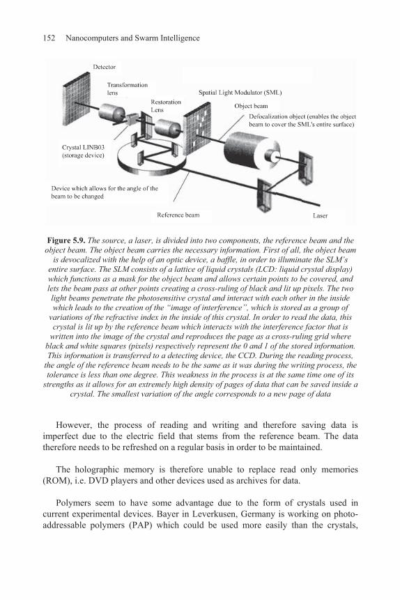
Figure 5.9. The source, a laser, is divided into two components, the reference beam and the object beam. The object beam carries the necessary information. First of all, the object beam
is devocalized with the help of an optic device, a baffle, in order to illuminate the SLM’s entire surface. The SLM consists of a lattice of liquid crystals (LCD: liquid crystal display) which functions as a mask for the object beam and allows certain points to be covered, and lets the beam pass at other points creating a cross-ruling of black and lit up pixels. The two light beams penetrate the photosensitive crystal and interact with each other in the inside which leads to the creation of the “image of interference”, which is stored as a group of
variations of the refractive index in the inside of this crystal. In order to read the data, this crystal is lit up by the reference beam which interacts with the interference factor that is
written into the image of the crystal and reproduces the page as a cross-ruling grid where black and white squares (pixels) respectively represent the 0 and 1 of the stored information. This information is transferred to a detecting device, the CCD. During the reading process,
the angle of the reference beam needs to be the same as it was during the writing process, the tolerance is less than one degree. This weakness in the process is at the same time one of its
strengths as it allows for an extremely high density of pages of data that can be saved inside a crystal. The smallest variation of the angle corresponds to a new page of data
However, the process of reading and writing and therefore saving data is imperfect due to the electric field that stems from the reference beam. The data therefore needs to be refreshed on a regular basis in order to be maintained.
The holographic memory is therefore unable to replace read only memories (ROM), i.e. DVD players and other devices used as archives for data.
Polymers seem to have some advantage due to the form of crystals used in current experimental devices. Bayer in Leverkusen, Germany is working on photo-addressable polymers (PAP) which could be used more easily than the crystals,

Elements of Technology for Information Systems 153
especially when it comes to industrial mass production. Bayer predicts commercial usage in the next two years.
Traditional mass storage devices have to extract the information from the medium before being able to consult it and compare it to the requested operations (this is the IT toolbox needed for production). In the case of holographic memory, the data does not need to be extracted to proceed to the operation that compares it to other sources.
The selection of data according to given criteria in data warehouses or datamarts consists of very long procedures that “kill” content management systems. The time needed to carry out a search is now much shorter.
This property is the biggest commercial advantage of this device for the next five years as it can be applied to systems which lie at the heart of large companies such as ERP, CRM or Business Intelligence. The first systems that will enter the market will be destined for the storage of data in companies.
A market study stated that the first applications will offer a capacity of 150 gigabytes on a removable disk with a format of 5 1/4". The speed of transfer is estimated to be at 20 megabytes/s for the writing and 40 megabytes/s for the reading process. However, this technology is not necessarily limited to disk type formats, but could be reduced to every 3D immobile device.
Figure 5.10. Four possible scenarios for the development of holographic storage devices

154 Nanocomputers and Swarm Intelligence
5.2.4. The technology of AFM memories
Atomic force microscopes allow for the exploration of all possible types of surfaces by only using the molecular force that the surface of the sample applies to the tip of the microscope (see section 3.1). The tip is in contact with the atoms of the surface and the vertical movement of the probe when it scans the sample’s surface horizontally. The atoms are detected optically. If the tip is covered with some form of metal, the variation of the magnetic field emitted by the probe, which swings from side to side at a high frequency, can be converted into images, i.e. meaningful data.
The technology of AFM (Atomic Force Microscopy) memory exploits this principle with the aim of increasing the performance of two-dimensional storage.
The concept stems from IBM’s laboratories in Zurich which already possess the STM and the AFM. This form of memory could be described as a nanoscopic version of the mechanical data storage used in the first computers, i.e. punched cards. However, this time the holes are “nanoholes”. Furthermore, the cards of the nanotechnological generation can hold more than one billion holes per mm². Theoretically, a density of storage of about 300 gigabytes/in² is possible. Tests have so far been limited to a density of 64 gigabytes/in².
The Millipede project developed by IBM in Zurich consists of developing a 3 mm squared device made up of billions of points derived from those of an AFM and aligning them on this square, like the bristles of a hairbrush. These points or probes only move on a square of plastic film of few mm2 in size in which they “punch” nanoholes, or on which they later detect these holes.
“Millipede” indeed refers to the creature and its ability to move all of its legs simultaneously. The system allows for reading and writing processes to be carried out simultaneously by activating several thousand tips at the same time.
The experimental setup contains a 3 mm by 3 mm array of 1,024 (32x32) cantilevers, which are created by silicon surface micromachining. Every tip (or probe, i.e. the millipede “legs”) has its own working zone, and all tips can write or read at the same time. In order for every tip to be able to read and write all positions in its zone, the grid on which the tips are affixed moves according to the X or Y axis, which are determined by the storage support device. At a particular point in time every tip will address the same position within its respective working zone. These movements of X and Y on the matrix allow the encoding device to read and write pages of data structures in tables (rows and columns) of binary data. Every pair in the position of (X,Y) corresponds to one page of data. An activation mechanism allows the selection of a pages (position (X,Y)) on the grid and ensures

Elements of Technology for Information Systems 155
the contact between the two points and support of polymers (position Z). A page of 1,024 bits is therefore read or written in one single operation, which is a step ahead of the relatively slow process of reading and writing of the best performing magnetic systems which are limited due to thermo inertia. The devices authorize very high transfer rates for two-dimensional memory approaching the 10 Mbps mark.
Figure 5.11. The technology of AFM memory, IBM’s Millipede project
The storage support device is made up of three layers: the first layer consists of PMMA (PolyMethylMethAcrylate) and corresponds to the support into which the hole is engraved. The second layer consists of Su8, a photosensitive resin which is there to stop the engraving process and directs heat from the tip to the third layer. The third layer is made up of silicon in order to absorb the residual heat. The second layer acts as a softer penetration stop that avoids tip wear but remains thermally stable (e.g. better quality of the holes and higher resistance towards heat, which is essential for the reading process).
The legs consist of tiny built-in girders whose ends remain free and are the mono-atomic tips of an AFM. Every leg is about 50 microns long and consists of two parts which allow for the circulation of two currents of different temperatures. The first current allows for a temperature of 350ºC which is used for reading the data. When the second current is added the temperature rises to about 400ºC, the temperature needed for the writing process. This tip penetrates the support and is stopped by the layer which is made up of Su8 and disperses the heat. As a convention, a hole corresponds to binary 1 and the absence of a hole to 0.

156 Nanocomputers and Swarm Intelligence
For the reading process, the tips are heated to 350ºC and the grid moves. Unless the tip encounters a hole, heat is dispersed and the strong decrease in the tension of the leg is interpreted as 1. Holes are detected when there is no strong decrease in the tension. These intervals are interpreted as 0.
One of the main challenges lies in the material used to create the support in order to allow for repetitive operations of the reading process without damaging it.
IBM’s researchers have tested two prototypes of ATM memory. The first one comprises five rows of five legs. The second one was previously mentioned and consists of 32 x 32 legs. These tests were mainly focused on different parameters such as the space between the holes, their diameter or the appropriate material for the support.
On the devices consisting of 32² disposing of 80% of functional legs, it is possible to write information with a density of 30 gigabytes/in². Another experiment showed that the density of 200 gigabytes/in² is accessible. It should be kept in mind that currently used hard disks do not exceed a limit of 80 gigabytes/in². During the test, the device was limited to one leg, which of course does not reflect reality. The density reached was several terabytes/in².
IBM believes that this type of device could be produced on a large scale and be commercialized in the short term, i.e. in the next few years. These devices could find their first applications in digital cameras and camcorders. They would be a strong competitor for flash memory because of their high capacity. However, some obstacles remain in the endeavor for mass production. These problems lie in the area of the stability of bits. The process of erasing and rewriting data also requires improvement. Furthermore, the density of storage and the number of legs need to be heavily increased in order to equip the first commercial applications and create a commercial advantage. Millipede 64² memories, consisting of 64 rows and 64 legs, are currently being tested. They are equipped with smaller legs and use a new schema of multiplexing in the activation device. Their energy consumption has been reduced, and in comparison to previous models like the Millipede 32² they offer a higher speed of data transfer.
5.2.5. Molecular memory
The idea of using organic and biological molecules taken from the world of living organisms, such as proteins, to encode, manipulate and restore information, has been explained in section 3.6.3.

Elements of Technology for Information Systems 157
A protein is a nanomachine whose molecular structure has been selected during evolution in order to fulfill a specific biological task.
We have seen how molecular memory use the photo cycle, which means that the structure of a molecule changes when it reacts to light. Here, photosensitive material is used in the cycle to change the protein from a stable state to another state, such as a messenger which encodes and then restores information. This can be compared to traditional RAM. The major property of this technology lies in the protein’s capacity to take on different three-dimensional forms and organize itself in the structure of a cubic matrix within a gel of polymers. Contrary to traditional memories that only use two dimensions to store information, molecular memories use three dimensions. In other words, the density of storage and the time required to access information (this device is based on parallel operations in terms of accessing data) have greatly improved. Their capacity lies within about 1 terabyte/cm3 and a speed of access of 10 Mbits per second.
On the basis of this technology, Robert Birge produced the prototype of a hybrid computer which consists of four main boards on which storage and calculating units are divided and specialized. The board within the main unit only contains circuits made up of semi-conductors. Two boards are equipped with memory based on proteins (digicubes based on bacteriorhodopsin), which are capable of storing a maximum of 40 giga-words. These boards allow random access without any mechanical part being used in the device as is the case of RAM within currently used computers. The other board allows for a more permanent and more economic storage. The fourth board contains an associative memory made up of fine layers of bacteriorhodopsin. The main advantage of such a computer lies in its exceptionally high storage of around one tera-word (1012 words). This capacity is particularly important for complex scientific simulations or cognitive systems based on programming techniques that lead to artificial intelligence.
5.3. Batteries and other forms of power supply
The on-going progress in processing speed, storage capacities, communication between different machines and bandwidth has reduced the size of computer systems. The era of mobility has begun. Whether it is cell phones, PDAs, laptops, handheld game consoles, or even more innovative equipment such as wearable computing (i.e. computerized clothing), all of these rely heavily on mobile energy sources. Who is not aware of the weaknesses in current power supplies after experiencing a flat battery in their cell phone or laptop?

158 Nanocomputers and Swarm Intelligence
The technology of batteries has evolved rather slowly compared to that of semi-conductors and mass storage devices. The rate of innovation only lies at 5 to 7% per year since the introduction of lithium technologies. Power supply, which has so far remained of rather little interest, has become a major challenge in the fields of portability and nomadic systems.
Current innovations of battery components are mainly being carried out in the domain of chemistry rather than in the domain of electronics. Today’s batteries work in the following way: they create a link between two chemical reactions, an oxidation process which generates negatively charged ions or electrons and a reduction process that consumes those electrons. Furthermore, a “path” is created which the electrons use to circulate from the negative terminal to the positive one. These “terminals” are a positive and a negative electrode put into an electrolyte solution which allows the current to circulate in the inside of the battery. The amount of energy in the battery is limited to the quantity of energy stored in it under the form of the materials that participate in the reaction. When the electrons circulate between the negative electrode (anode) and the positive electrode (cathode), the battery generates energy while simultaneously discharging itself.
Improvement in this process currently relies heavily on the widely known technology of nickel-cadmium batteries (NiCd) and nickel metal hydride batteries (NiMH). New emerging technologies such as lithium-ion, lithium-polymer and zinc-air batteries are the focus of research. Progress in the field of nomadic systems and the increasing commercial demand for them is stimulating the development of conventional batteries and also making way for alternative solutions that do not have to rely on the progress made by the chemical industry. These are systems using kinetic energy to recharge batteries.
For ubiquitous computing and the generation of objects that communicate with each other, new approaches are currently being tested. These are power supplies generated from the world of living organisms, microcombustion engines, nuclear batteries and other devices that are very different from traditional batteries. Scientists are currently carrying out experiments on solutions capable of supplying micro and in the future nano-objects with energy that stems from living organisms, such as energy taken from spinach, sugar, slugs or flies. These new sources of energy use ATP (Adenosine TriPhosphate) molecules which store phosphates of high energy in order to store energy just like in the muscles of living organisms.

Elements of Technology for Information Systems 159
Figure 5.12. Because of the presence of bonds which are rich in energy (bonds that link groups of phosphates are anhydride acid bonds), living beings use ATP to provide energy for chemical reactions that require them. The ATP molecule consists of three different types of units: a nitrogenous base called adenin, a 5 carbon atom of the pentose sugar called ribose and three groups of phosphates (H3PO4). The chemical bond between the second and the
third phosphate can easily be created and also be easily detached. When the third phosphate detaches itself from the rest of the molecule, energy is released.
The miniaturization of ambient molecular objects is not only limited to electronic circuits. To miniaturize any kind of technical object down to the micro or nanoscopic level, all technical functions need to be taken into account. This is more than just the integration of proteins and integrated circuits. Mechanical devices and the power supply that is needed for objects that are too small to be recharged on a regular basis need to be considered. Two approaches to these power supplies are currently being researched. One is embedded micro-batteries which rely on the conversion of chemical energy by a mechanical force. This process relies particularly on one protein, kinesin, which is present in all cells that possess a nucleus (eukaryote cells). This protein transforms chemical energy of the ATP molecule, which can for example be found in muscles, into mechanical energy
5.3.1. Lithium-ion and lithium-polymer batteries
The lithium-ion battery is currently used in the majority of portable equipment from laptops to cell phones as it is relatively small and light. Currently, this battery supplies the strongest specific energy (energy/mass) and is of the highest density of energy (energy/volume). It consists of a carbon anode and a lithium cathode, i.e. oxide transition metal whose valence electrons can be found on two layers instead of just one. An organic solution is used as the electrolyte. The disadvantage of this kind of electrolyte is that it is very flammable. In “traditional” batteries, the tension between the electrolytic poles lies at about one to two volts per cell. The lithium-ion battery generates up to four volts per cell which explains its excellent performance in terms of specific energy. For a large number of applications, the lifespan of this battery may reach seven to 10 years. The lithium battery using thionylchlorid has a

160 Nanocomputers and Swarm Intelligence
lifespan of 15 to 20 years, offers the highest energy density in its group and it also discharges itself at a low rate. These batteries are therefore very well adapted to applications for which access to the battery in order to replace it is very difficult.
Lithium-polymer batteries are the next generation of lithium-ion batteries. They are marked by the advantages of lithium, such as being lightweight. At the same time they do not have the inconveniences of the lithium-ion batteries (e.g. they are very flammable, discharge themselves more quickly, etc.). In the case of lithium-polymer batteries, instead of a liquid electrolyte, a solid polymer substrate is used. The lithium ions are incorporated into this substrate so it can be easily worked on. This type of battery is environmentally friendly and is lighter and more reliable; it does not require a metal case which usually harbors the liquid components of batteries of the lithium-ion group. As they do not need the metal case, lithium-polymer batteries can take the shape of very thin pieces of paper, making way for a much wider field of applications.
5.3.2. Zinc-air batteries
The zinc-air battery has one very original property: it uses the oxygen of the air surrounding it. The oxygen therefore does not need to be stored in the electrolyte. This group of batteries consists of a zinc cathode and a graphite anode. It uses the atmospheric oxygen as an electrolyte. These batteries offer a much higher density of energy than the majority of alkaline batteries. They are equipped with functions that block the circulation of air during the charging process and when in a passive state. These functions also ensure ventilation of the cells during the discharging process which allows for an increase in energy and limits auto-discharging in the passive state. The lifespan of this type of battery is generally five times longer than that of other products on the market.
By using oxygen as the electrolyte, this technology allows for a smaller battery. On the other hand, air also contains elements that may damage the battery: steam from water and carbon dioxide are the two main ones. Variations in the air’s humidity can significantly affect performance. Furthermore, carbon dioxide forms carbon crystals in the cathode that are supposed to block the circulation of air which leads to less energy being delivered and also limits the cell’s lifespan. The layout of the tube through which the air circulates is essential, it may be long tubes with a rolled-steel equipped with sections of hydrophobic membranes. This system keeps most of the steam from the water in the air outside and therefore allows for an efficiently working battery even under the worst conditions.

Elements of Technology for Information Systems 161
Figure 5.13. The zinc-air battery uses the oxygen in the air surrounding it. The oxygen therefore does not need to be stored in the electrolyte
5.3.3. Micro-batteries
The implementation of embedded microsystems whose capacitors, processing units, activators or transmission systems are integrated into areas which are difficult to access (such as the engine of a vehicle, on a moving part or inside the human body) is indeed very difficult. This is why embedded microsystems need their own source of energy. Furthermore, the microsystem and its power supply cannot exceed the sub-millimetric dimension.
Developing a “traditional” battery on this level is, of course, impossible.
A new generation of batteries, the size of the width of a hair, with a density of energy which is 100 times higher than that of “traditional” batteries, is currently being developed. These batteries are constantly recharged by devices that recover energy through magnetic vibration (see section 5.3.5), offering long term independence from a stable power supply to embedded microsystems.
The concept’s originality lies in its production and the research of new materials, which were used as electrodes in the form of very fine layers. The components V2O5

162 Nanocomputers and Swarm Intelligence
and FexV2O5 were used as positive electrodes in lithium batteries. Instead of putting the battery together piece by piece, as is the case for traditional batteries, the technology derived from the production of semi-conductors is applied. This technology relies heavily on the process of photolithography.
Such a process is much simpler than the traditional production of batteries and can be easily used on the micron level. Furthermore, it also allows for the usage of materials of a remarkably high level of purity.
This kind of power supply will be used in the first applications of embedded microsystems that are implanted into the human body. These systems will, for example, be able to regulate the level of insulin in a diabetic patient. These systems need to be perfectly autonomous and their lifespan needs to be several years.
5.3.4. Micro-batteries using nuclear energy
Atomic engineers at the University of Wisconsin, Madison have explored the possibilities of producing minuscule batteries which exploit the decrease in the number of radioactive nuclei of substances such as polonium or curium to produce electric energy. They can therefore be used as a weak power supply. These devices, which are similar to MEMS (Micro Electro-Mechanical Systems; see section 5.6), measure between 60 and 70 microns.
These micro-batteries are very light and deliver enough energy to function as a power supply for nanodevices.
The energy released through the decrease in the number of radioactive nuclei is transformed into electric energy, which is restricted to the area of the device that contains the processor and the micro-battery that supplies it with energy.
The decrease in the number of radioactive nuclei releases electrons that shoot the negative pole of the battery and create a difference in the potential which then leads to an electric current that supplies the micro-equipment with electricity. To avoid the electrons reaching the negative/positive pole in a neutral state, a “void” is created between the two poles and the electrons are forced to pass the radioactive material at the negative pole through a minuscule conductor line. Ambient energy that is released by the radioactive substance does not entirely consist of charged particles (electrons that will create electric energy) but most of it is released under the form of heat which could be used as a form of power supply by the micro-equipment.
The energy supplied by this kind of device is measured in microwatts or in milliwatts. This type of source can supply energy for small portable devices,

Elements of Technology for Information Systems 163
chemical receptors and micro-laboratories (lab-on-chip). Scientists are already planning the production of microsensors based on this type of power supply. These sensors will be added to the oil that ensures the smooth running of heavy machinery. In this way, they carry out a local micro-control for an improved maintenance of the machinery.
5.3.5. Recharging batteries with the help of kinetic energy
This principle is based on the conversion of kinetic energy into electrical energy in order to recharge a battery, for example, the alternator of a car through which connection with the combustion engine constantly charges the battery. A large number of research projects are being carried out and some of them are close to being introduced to the market. Compaq has put a patent on a device that uses the mechanical energy of typing on a keyboard to recharge the battery of the laptop in use. This principle is very simple and consists of connecting every key with a small magnet around which an inductor is wrapped. Each time one key is hit the magnet creates a magnetic field which is converted into electric current that then charges a capacitor. When the level of energy in the capacitor is high enough, the energy is stored and transferred to the battery.
The concept of large wireless microsystems that exchange information relies on minuscule systems which are autonomous when it comes to power supply. However, this autonomy is limited by the spread of a high number of batteries used in a certain network of objects (see section 6.4). They are a major source of pollution. The solution might lie in recovering energy (mechanical, chemical, thermal or radiant) in the surrounding area of the systems in order to make them autonomous during their lifespan. Recovering energy through mechanical vibration, used, for example, on moving vehicles or in industrial machinery, is currently one of the most researched solutions in this field. With the help of mechanical converters using silicon technology whose frequency lies around some 10 Hz and vibrates with the amplitude of some hundred microns, a device may have the power of around one microwatt per gram of mass. The power the device may use is around several miliwatts and therefore compatible with the energy the equipment requires to function.
5.4. New peripheral devices and interfaces between humans and machines
The concept of pervasive technology characterizes a new generation of information systems, relies on two principles and goes much further than miniaturization or increases processing and storage capacities. These are the

164 Nanocomputers and Swarm Intelligence
“democratization” of devices in terms of the price and the development of a better interaction between humans and machines.
Human computer interaction (HCI) tends to erase the notion of an interface by merging reality with the world of machines. As technology is increasingly used in our daily lives, such as receptors or other devices that are placed underneath our skin, or the use of electricity produced by the human body which is used as a power supply for appliances that lie on our skin, progress in this field will allow for an osmosis of technology and the human body. The development of these interfaces often merges current scientific disciplines in research and development. The more our environment is interlinked, the more we need to adapt access to fairly complex information.
If traditional keyboards and screens of the new generations remain the principal means of information exchange between our world and that of information systems, new possibilities for the machines to obtain information should be created.
On the one hand, these new approaches allow computers to obtain information and orders from the user in a more natural and anthropomorphic way. Peripheral devices allowing for the entering of data will be an extension of the human body. Some of these systems which are already operational have even been commercialized, while others are still at the prototype stage. They mainly include functions such as eye tracking, recognition of gestures (handwriting recognition has been applied to the keyboards of certain devices for several years now) and voice recognition, which is well known and a rather basic device. Highly pervasive systems or “diluted” information systems can use other channels of information exchange. This exchange is more than the communication with the macroscopic world of humans (voice and gestures) and the world of machines (receptor of position, temperature, pressure, etc.). The desired information is of a microscopic nature from minuscule systems often integrated on just one chip which can hardly be distinguished from the surroundings it controls.
Another aspect of the interface between humans and computers of the new generation is the concept of recovering and visualization of data. “Electronic paper” is a device that possesses the characteristics of traditional paper; it is very fine, light and flexible with clear contrasts once something is written on it. It is also able to maintain the visualization of information when it is not connected to a power supply. Furthermore, it can be reused i.e. the content can be erased and new content can be uploaded. This is one of the new visualization devices which has recently entered the market. If an antenna is integrated into a sheet of paper it can receive data via radio waves from a newspaper for example, and visualize the content with help of the electronic ink that can be found in the paper.

Elements of Technology for Information Systems 165
Apart from this example, other visualization devices of multimedia content are being developed to fit all possible situations in daily life. In the short term, successors of LCD screens will be developed which do not need their own source of light to ensure the visualization process. This weakness is a disadvantage of the LCD screens that took over from the “antique” CRT (Cathod Ray Tube) screens. LCD screens still use too much energy, are too heavy, too thick and too fragile for large-scale distribution. Research is being carried out into devices which can generate their own source of light by recycling the light available in their surrounding area in order to ensure their own light source.
In the case of laptops, their screens use most of the electrical energy. The goal of ubiquity and pervasive systems is based on a massive diffusion of mobile and portable devices. However, it is currently being hindered by the visualization multimedia content.
OLED screens, for example, emit visible light from any angle and allow for more realistic and clearer images. They also consume less energy than LCD screens and are much cheaper in production. As they are very slim, they are compatible with the idea of electronic paper and the mobile usage which characterizes the new generation of our information systems.
As the subject is very broad, there will be no detailed elaboration about new technologies in the fields of video and photography as it will take us too far away from the original topic. Some of the emerging fields will still be mentioned in order to give an overview of the new generation of computers including the visualization of information for the user.
5.4.1. Automatic speech recognition
The interface between humans and computers has evolved since the appearance of the mouse and more recently with touch screens. All interfaces use mechanical force that is applied by the users’ hands and fingers. Since the mid-1990s, automatic speech recognition (ASR) has been developed as an extremely efficient alternative for communicating more naturally with information systems of embedded systems.
The first application took place in the Bell laboratories in 1952 when a team of researchers developed a wired logical system that allowed for a computer to identify 10 decimal numbers and the words YES and NO. The device imposed an extremely slow rhythm of speaking and did not accept the slightest variation in the articulation of words. Pauses of a tenth of a second were taken between each word and were used as a separator. The first systems could only be used by one speaker and often

166 Nanocomputers and Swarm Intelligence
required a long learning process before the machine could process the data delivered by the user.
Even today, machines can process several hundred words but the learning process is still long as the machine needs to save a sample of all those words it is supposed to “understand”. Systems that can process an even larger vocabulary, i.e. several thousand to several hundred thousand words, ask the speaker to recite a group of sentences which will be analyzed by the interface in order to establish the parameters of a model.
Today, systems which allow for several speakers to use them only exist with a very limited vocabulary (some words and 10 numbers). They are used for voice mail applications or for dialing numbers orally.
At present, not every field is experiencing progress due to this new generation of technology. It is used for voicemail in telephones, dialing numbers without using our hands, in more complex transactions in ERP applications and, last but not least, as a form of signature. Our voice is, of course, much easier to imitate than digital fingerprints or eye scanning.
These applications allow for the installation of a natural interface with the capacity to dictate directly to a computer that is able to understand up to several hundred thousand words and whose vocabulary can be extended by the user’s own specialized vocabulary. Even when already using both hands, for example when driving, the user is still able to do business, the same way as with a real assistant: the user can dictate a text or give orders, and also ask for certain research to be carried out or the opening of a folder. This is the case for a highly elaborated interface such as structured query language (SQL) or any other fourth generation language. In warehouses and on logistical platforms, voice recognition is increasingly used to carry out transactions that are relative to supply chain management, i.e. the system that controls entire processes from the warehouse to the ERP. The forklift truck operators can carry out these operations while driving a forklift truck. Before the introduction of voice recognition they were forced to stop driving to carry out administrative tasks. Vocal recognition is an interface whose potential of productivity in the administrative sector is far from being used to its full potential.
The process of voice recognition consists of three main functions: analysis of the received signal (front-end), learning process (training) and recognition (back-end).
Our voice is a sound wave produced by the mechanical vibration which is carried out due to the flexibility of air in the form of analog. The vocal signal is caught by a microphone and digitalized with the help of an analog/digital converter. The human voice consists of a multitude of sounds, most of them repetitive. The signal is

Elements of Technology for Information Systems 167
generally compressed in order to reduce the time of processing and storing it in the memory. High performance applications on the market use highly reliable microphones and DSPs (see section 4.2.3) to ensure the high quality of the received signals, quickly produce samples and easily separate all other noise from the vocal signal. Standard applications use the PC’s own microphone and sound card.
The first step consists of creating parameters for each signal, i.e. producing a characteristic sample of a sound which is then used to recognize it later on. There are several methods to do so, the most widely used ones are spectroscopic or identification based.
Spectral methods bring the sound down to its individual frequency without identifying its structure. In fact, the sound superimposes several sinusoid waves. By using an algorithm known as the Fast Fourier Transform (FFT5), different frequencies which make up a sound are isolated. By repeating this process several times a characteristic sample of the sound can be obtained.
Another approach called the identification method is based on the knowledge of how sounds are produced, for example, how the air passes the vocal cords. The buccal artery consists of a cylindrical tube of an altering diameter. Adjusting the parameters of this model allows for the determination of the transfer function at all times. The resonance frequency of the air passing the vocal cords can be captured. These resonance frequencies correspond to the maximum energy of the spectrum. By repeating this process a sample of the sound is created.
The signal is then sub-divided into workable units. The identification of long units such as syllables or words is complex but allows for easy recognition. Basic sounds would be much easier to identify but are not very reliable in the field of actual voice recognition. The compromise between these two is to take the smallest linguistic units which do not have meaning themselves but change meaning when used in different positions. In French, for example, there are 36 of these units, out of which 16 are vowels and 20 consonants. The French word “dans” (inside) consists of [d] and [ã]. The identification of segments is based on phonetic and linguistic limits of language (e.g. articulatory phonetics, the sounds of a particular language, phonetics, intonation, syntax, semantics, etc.).
The training function enables the program to create a link between elementary units and the act of speech with its lexical elements. This link uses statistic modelization such as the Hidden Markov Models (HMM) or an Artificial Neural
5 The FFT is a mathematical tool used for processing signals. It associates a spectrum of a frequency with a non-periodic function.

168 Nanocomputers and Swarm Intelligence
Network (ANN). To create a dictionary that contains the acoustic references, the interlocutor pronounces the entire vocabulary used several times.
An Artificial Neural Network (ANN) is a model of data processing that directly links to artificial intelligence as it is inspired by the functioning of neurons, i.e. the way our brain cells process, learn and store information. The main applications of neural networks are the optimization and the learning process.
A neural network consists of a large number of basic cells that are interconnected, i.e. a large number of parallel calculating units. An elementary cell has a limited number of entrance and exit gates and can manipulate binary digits and numbers. Binary digits are represented by 0 and 1.
This kind of network consists of simple processing/calculating cells (neurons) which are interconnected through bonds affected by weight or a weighting system. These bonds (or channels) enable each cell to send and receive signals to and from other cells in the network. Every one of these bonds is assigned to a weight which determines its impact on the cells it connects to. Every neuron has an entry gate that allows it to receive information from three different types of sources: other neurons, the activation function which introduces a non-linearity to the working of the neuron and the exit function which states that the result of the function carried out is applied to the neuron itself. In a neural network with N cells in the first layer C(1)..., C(N) and a weight of N assigned to the bonds w(1)...,w(N), the entrance gate of a cell in the second layer is generally the sum of the weight of bonds connected to the preceding neurons:
X = w(1)*C(1) + w(2)*C(2) + ... + w(N)*C(N)
Neurons or cells that process information are able to learn by adjusting the weight of their connections. The learning process consists of determining the optimal weight of different bonds by using a sample. The method which is most commonly used is known as retro-propagation: using the values applied to the cells on the entrance gate and with the errors obtained at the exit gate (delta), the weight is corrected according to the weighting system. This cycle is repeated until the rate of errors of the network stops increasing. If this process is carried out for longer than that, the network’s performance decreases. This phenomenon is known as an “over trained” network.
In the field of voice recognition, the neural networks are largely used in the isolated recognition of words, syllables and phonemes. The increasing demand in the field of continuous speech acts (i.e. a speech, sentences or words that are linked to each other and cannot be separated) progressively increases the usage of neural networks treating the continuous flow of the voice’s signal in real time.

Elements of Technology for Information Systems 169
Voice recognition consists of recreating (back-end function) the most likely text. In order to do so, the machine ensures the concatenation of the elementary segments of the speech act in the form of a target text. Two approaches, one global the other analytical, allow for the recognition and comprehension of words.
In the global approach, the word is the basic unit and is considered as a whole entity which should not be sub-divided into smaller units. The system has an acoustic sample of every word and can therefore identify them. In order to do so, every word is pronounced at least once in the learning process and allows for the storage of this knowledge. The global approach avoids co-articulation, i.e. the assimilation of the place of articulation of one speech sound to that of an adjacent speech sound and leads to the sounds having an impact on each other within a word. However, this approach limits the vocabulary and the number of interlocutors. In fact, the recognition of isolated words requires a memory of considerable size to store all acoustic samples of all words in the vocabulary and an enormous processing capacity to compare an unknown word to all other words in the dictionary. Furthermore, it would be unrealistic to expect the user to dictate the entire vocabulary.
The analytical approach uses the linguistic structure of words. The basic units which are recognized are phonemes or elementary syllables. The analytical approach has a richer vocabulary as it is sufficient to record and save all principal characteristics of the basic units in the machine’s memory.
Today, the demand is constantly increasing in the field of systems that allow the user to speak continually, i.e. naturally just as if the user was speaking to another person. Current voice recognition systems allow the user to dictate naturally and the words appear on screen with a delay of three to five seconds. Modern processors work at more than 1.5 GHz and have a memory of more than 1 megabyte, so this delay can be reduced even further. The recognition of continuous speech acts differs from the recognition of single words. In the latter case, gaps of several tenths of a second have to be left between every word which greatly reduces the difficulty of the task.
The recognition of continuous speech acts requires a signal to be broken down in order to identify the different words or phonemes within it. There are two different approaches.
The first consists of recreating a sentence from the signal. This approach is becoming increasingly popular. A signal is simply read without trying to understand its content; the focus lies entirely on decoding it. However, for every part of the sentence this method needs to search all of the words its dictionary contains. This operation is often of an unpredictable length of time, or simply takes too long.

170 Nanocomputers and Swarm Intelligence
Another approach uses anticipation to recognize words. This concept is similar to our brain which also uses the context to anticipate the end of a sentence. Equipped with “certain intelligence”, the system can anticipate what will be said: a telephone conversation usually starts with “hello” and is followed by “Mr” or “Mrs”, often followed by one of the names in the contacts list which the machine will then search for. This approach avoids the lengthy search in the dictionary and saves a lot of time.
In practice, no system is entirely based on a top-down or bottom-up approach only. In both cases, the vocabulary would be extremely limited. Operational systems use an approach that combines both technologies.
5.4.2. Gesture recognition
The use of gesture recognition as a human/machine interface used to transmit orders is as old as the first machines themselves. It is a hand or foot movement that transmits the order to the machine. Apart from the keyboard, the gesture recognition of computers also includes pens, graphics tablets, the mouse and other joysticks used for the first graphical applications. The keyboard as the sole interface no longer fulfils the task.
Today, these different types of interfaces are being improved by other sensors, for example, gloves which allow the machine to detect and interpret all forms of a body’s gestures including facial expressions. However, an increasing amount of applications no longer need restraining receptors but use the signal of a camera (visible light or infrared) to detect movement. These cameras are today mainly used to follow hand movements as well as eye movements. Applications in this domain do not rely on conventional equipment but use algorithms to allow for an efficient interpretation of visual images by the computer.
The majority of the applications in this domain are used in experiments in virtual reality with in the field of sports. They are also used as simulations and moreover as a supporting tool that helps disabled people to communicate.
At the end of the 1990s, a group of researchers from the University of Carnegie Mellon, USA and the University of Karlsruhe, Germany combined vocal recognition and gesture recognition in a single interface. The aim was to create an interface which was capable of almost natural communication. It can read lips, interpret handwriting and even detect facial expressions and someone’s eye movement.

Elements of Technology for Information Systems 171
5.4.3. Processing and recognizing writing
Processing and recognizing writing are specialized domains in the field of gesture recognition. This principle is already fairly well known and widely used in applications such as PDAs, smartphones and Tablet PCs which use a program that recognizes handwriting and touchscreen panels.
Handwriting recognition is an application that transforms handwritten texts into typed text. The application enables the user to write text with a special pen onto a window which is visible on the touchscreen panel and to obtain its transcription in the form of typed characters.
The new generation of mobile/portable Tablet PCs has this function which enables the user to take notes and use them in traditional or innovative ways.
Tablet PCs digitalize handwriting and transform it into typed characters with the help of an electromagnetic input/output device or a touchscreen panel. The handwriting is then analyzed by a recognition program which is part of Microsoft’s Windows XP Edition Tablet PC. This program is based on several thousand handwritten pages in different languages which were used as a sample. The process of handwriting recognition identifies every individual word. It separates all lines and curls the user draws to write a word. By using a specialized pen the user can, for example, directly write his/her text on the screen of their Tablet PC. By drawing a box around a part of the text and ticking the center of it, this part of the text can be moved very easily as its movement is linked to that of the pen. This concept is called digital ink.
Two different types of devices are currently available: graphics tablets and touchscreens, i.e. screens that can be used as a digital notepad. Technical progress in devices that process either graphic images or handwriting is paving the way for new tools such as digital pens which could be used on any kind of material just like traditional pens. This kind of device is no longer dependant on the link between pens and digital notepads or pens and touchscreens.

172 Nanocomputers and Swarm Intelligence
The displays of touchscreens are often made of glass and are equipped with piezoelectric transducers as emitters and receptors for the X (lines) axis and the Y (columns) axis. The touch screen’s control unit sends an electrical signal of a high frequency (several MHz) to the transducer which then alters the ultrasonic waves in the glass. These waves are sent to the surface of the touchscreen with the help of a series of reflectors. These reflectors placed facing the transducers redirect these waves to the transducer which transforms them into an electrical signal.
By touching the screen, the user absorbs part of the wave that goes through it. The received signal will be compared to the card, or the stored digital matrix, and the detected changes allow for the calculation of the coordinates of a specific point. This process works independently for the X (rows) and the Y (columns) axis. By calculating how much of the wave is absorbed, the Z axis, indicating depth, is also generated. The digital coordinates are transmitted to the computer for further processing.
A digital pen works just like a graphics tablet. It stores the trajectory (x(t),y(t)) of a pen and does not limit itself to the X and Y coordinates of an image, such as a bitmap. This trajectory enables us to understand the movement and potentially the recognition of handwriting, which is crucial information for software dealing with this issue. Intel’s digital pen is a traditional pen that is equipped with miniaturized accelerometers and pressure sensors made up of silicon (the epitaxy of a layer of several microns of silicon in which strain gauges are used). The trajectory of every movement of the pen is captured, stored and transmitted to the computer which then converts these movements into a digital text. The paper (or any other surface that is used) apart from its traditional role of storing content, can be printed out with minuscule geometric images that indicate the positioning of the pen and allows for the identification of the page which is used in order to link it to a particular application.
IBM developed a digital clipboard which could replace traditional note pads. The digital clipboard captures the trajectory of a pen which is equipped with a transmitter using radio waves.
5.4.4. Eye tracking
With the era of the Internet, studies in the effectiveness of advertising messages that lead to the sales of commercial spaces, and research in the field of the visual aspects of pages that appear on screen have strongly developed over the past 10 years. This research has mainly led to the development of eye tracking. These systems have continually developed during this period. Over the years they have

Elements of Technology for Information Systems 173
become more flexible and less restraining and “invasive” to the user. Today they pave the way for new applications in the human/machine interface.
Eye tracking is a method of capturing the position of our gaze, i.e. where we look. Amongst all techniques in this domain, the corneal reflection is one of the most commonly used. It allows for high precision of the data taken but does not restrain the user’s movements. Several infrared light beams are sent by a group of diodes situated in the center of the pupil. The infrared reflections that are sent back by the cornea of the eye are detected and enable the user, after processing the data, to determine the center of the pupil as well as its position when focusing on the target object.
A system that analyzes the data can then retrace the eye movement of the pages that were looked at and gives an indication of which parts of the page were looked at for how long, the so-called GazeTrace.
The idea of using eye tracking as a means of communication and control for patients with physical disabilities led to the creation of a high number of research projects. 40,000 patients in Europe and the USA could possibly benefit from this kind of interface. However, currently only several hundred patients use this new form of technology. On the other hand, this type of application is far from being the only target for the technology of eye tracking. Any other user could be interested in this technology when wanting to use a system in situations where other parts of the body, such as legs and arms, are already used to carry out other tasks, i.e. while driving, operating an engine, etc.
Consulting and managing graphic environments in a virtual reality is based on other applications which are similar to this kind of interface. They are operated visually and are also very promising. The initial presentation of a page could be an (macroscopic or global) overview of graphics. The eye focuses on a section of the graphics and a zoom is used so this section increases its size in proportion to the rest of the page.
5.4.5. Brain machine interface
Brain machine interface (BMI) or brain computer interface (BCI) are interfaces that link the brain directly to the machine. This type of periphery is fundamentally different to all other kinds of interfaces between humans and machine: this kind of connection does not require any kind of transformation of a signal emitted by the brain’s activity expressed in the activity of muscles (psychomotor). The latter is usually used as a signal transmitted to the machine. The speed of a usual chain reaction (brain, nerves, muscles, human/machine interface) can be now be decreased

174 Nanocomputers and Swarm Intelligence
to several tenths of a second. Furthermore, other parts of the body such as hands, feet and eyes are free to carry out other tasks simultaneously. Military research is investigating this new technology which would enable a better coordination of fast and complex operations in a combat situation. Civilian applications may also take place in many different fields such as planes or using complex engines to carry out other tasks while driving, or in the field of crisis management, fires, etc. One possible application of this interface is to allow people who have lost their physical abilities or their senses to recover them artificially. In co-operation with the latest developments in the field of electronics, programming and cognitive science, a paralyzed person could drive a wheelchair with their thoughts.
Two approaches to this technology are currently being exploited.
The first approach uses the electromagnetic fields which are generated on a macroscopic level by virtual dipoles which represent the sum of all activities of a large number of neurons. In other words, all human activities generate a cerebral activity which is represented by the activation of the equivalent zones in the brain. When one of those zones is activated, a small electric current and a small magnetic field induced by the activity of 105 to 106 neurons can be measured. Two types of instruments allow them to be captured: electroencephalogram (EEG) or the magnetoencephalogram (MEG). The EEG measures the electric potential, i.e. the dipolar parallel feedback at the axis of the dipole. This feedback is diffused and affected by the tissue and sensitive to deeper lying sources. The MEG measures a magnetic field, i.e. a dipolar signal perpendicular to the dipole’s axis. This type of feedback is very focused and hardly affected by the cerebral tissue. It is not very sensitive to deeper lying sources. Due to price and practicability, BCI interfaces are used in combination with EEG instruments.

Elements of Technology for Information Systems 175
Figure 5.14. The EEG, a macroscopic approach of non-invasive neural interfaces
The EEG measures the macroscopic current underneath the scalp. Its simplicity represents a fundamental advantage in the development of cerebral interfaces: it is non-invasive, which means that it does not require an operation to implant electrodes or other linking devices to connect the brain to the system. The link is simply made through sensors which are placed on the head and are held in place by a hat or a hairband. These sensors capture cerebral waves and after decoding and processing them they transmit them to a computer.
The second approach is invasive and consists of implanting inorganic components which are connected to the neural system, i.e. directly implanted into the brain to create a link between movements and electric impulses. This approach is nearly microscopic and allows for the detection of the activity of a small group of specific neurons. However, this technology, as it is invasive and less reversible, is less adapted to operational cerebral interfaces which are ethically acceptable. It is used as a tool that allows for brain mapping, i.e. a detailed comprehension of the functioning of the brain, or more precisely the neural code which comes into play to activate or deactivate different neurons during all human activities. Before humans can finally use brain/machine interfaces to control the technical devices in their daily

176 Nanocomputers and Swarm Intelligence
life, they need to investigate on a much larger scale how the brain transmits its orders to organs. This knowledge can be obtained by a study of data captured on neural activity over long periods of time. Researchers at the Duke University Medical Center have tested a neural system by capturing the signals at the level of a neuron with the help of several invasive electrodes which were implanted into the brain of an ape. The team of researchers was able to recombine the signals emitted on the neural level and, with the help of a program running on an external computer, the arms of a robot could be controlled. The ape was encouraged to move the artificial arms by providing it with food that could be reached with the artificial arms. The experiment was successful. It was later reproduced by sending the signal that controlled the artificial arms through the Internet and allowed the arms to be moved more than 1,000 kilometers from the ape’s location. In 2002, the department of medical imagery at Duke University developed a telemetric circuit that allows the acquisition and the transmission of data through the skull without needing a sensor implant with cables which transmit information.
Since 2000, the results of research on non-invasive techniques which could be exploited industrially have breached all previously anticipated limits. The European project ABI (Adaptive Brain Interfaces) favors this approach and developed a cerebral interface based on the mental state of the individual in 2000/2001. In other words, every mental state corresponds to a precise activity. Equipped with an EEG on the person’s head that measures cerebral waves, the user can learn to use the interface by forcing him/herself to present a clear and distinct mental state to the device each time s/he wishes to control the computer by his/her thoughts. For example: relaxation, mental focusing, imagination of moving the arm, a hand, etc. The system is based on a neural network that learns to associate the user’s mental state to the respective activity. Five mental states are required to move the cursor on the screen. These are up, down, left, right and click. The ABI project showed that the user can play a computer game by simply thinking and edit a text with the help of a mental keyboard that appears on screen. Projects creating neural prostheses by BrainLab at the University of Georgia, USA use similar procedures. A non-invasive device captures the cerebral waves via EEG and enables the user to move a cursor by thought, or even command a wheelchair. At the beginning of the 1990s, the US Air Force were already carrying out experiments using BCI by enabling the user to control the flight simulator by thought alone. Only four non-invasive electrodes were used.
However, the researchers encountered two major difficulties. The first was the complexity of learning how to use the simulator. The users needed to concentrate in order to be in a mental state that enabled them to carry out a specific action. Furthermore, in order to interact with the machine and for it to run smoothly this mental state needed to be held and repeated several times. It takes several weeks or months for the user to learn how to interact with the machine effectively. The

Elements of Technology for Information Systems 177
rhythm of choosing letters in the ABI project is very slow. 22 seconds are required per letter. This is far from BCI’s goal to create an extremely high reactivity. The second difficulty is due to the procedures of a macroscopic nature. The required signal gets lost in a magna of “noise” or other undesired signals, and information is detected which is not useful. EEG waves are diffused and highly affected by the tissue; they represent the activity of nearly one million neurons. As the signal theory shows us, the risks of not detecting signals or detecting a false alert will be high until a reliable model that overcomes this weakness is found.
The usage of P300 waves currently represents a perspective in the process of
creating EEG-based, non-invasive and more reliable cerebral interfaces. For about 30 years, neurobiologists have been observing reactions to exceptional but expected stimulus such as going through a red light or a stock market crash. After 400 milliseconds an electric signal which is typical for our brain is sent out, which neurologists call P300. The P300 wave indicates the cognitive process of decision-making. In 1999, a team of researchers at the University of Rochester, USA, showed that the P300 wave is the universal “symbol” of a thought linked to an “expected surprise” and always leads to a reaction of the subject itself and might involve the tools used (computer, machine vehicle, etc.). This universal reaction could be an essential property usable in systems of telepathic control.
A team of researchers at the Technical University of Graz, Austria has developed a system that enabled a young paralyzed person to move objects with his left hand. This system combines the interface brain/machine (BCI) with an electric muscle stimulator. Thinking is an activity that requires our nerves and produces low electric currents within our brain. These currents are captured by the EEG, amplified and analyzed by a computer which selects those thoughts that express the desire to move the object from all of the patient’s thoughts. This filtering process is possible because of one physiological particularity of our brain. Half a second before carrying out a movement, the brain produces a specific EEG that predicts the movement. By concentrating on that movement, the handicapped person, whose brain is linked to the BCI via electrodes, provides the computer with the required information which activates the muscle stimulator that is linked to the young man’s forearm. Today, this young man can open and close his hand again simply thanks to the transmission of his thoughts.
5.4.6. Electronic paper
Trying to replace traditional ink and paper with electronic alternatives while preserving the advantages of traditionally used paper is something all electronic laboratories have been working on over the last decade. Electronic paper is a new visualization device whose qualities are flexibility and manipulation (i.e. it is
178 Nanocomputers and Swarm Intelligence
flexible and fine), just like traditional paper but which can be updated electronically. It works due to electronic ink that is integrated in this device. Generating and updating the text consumes small amounts of energy. Maintaining the text on the paper so it can be read does not consume any energy.
This principle dates back to 1977. Nicholas Sheridon, a researcher at Xerox’s Palo Alto Research Center (PARC), had the idea of replacing traditional ink by minuscule two-colored spheres placed between two slides of plastic. After 18 months of research the project was stopped as Xerox invented the laser printer. The emergence of the first generation electronic books and promising developments at MIT’s Media Laboratory of applying electronic ink to paper, plastic and metal have encouraged Xerox to recommence research and development of Sheridon’s idea.
The prototype of the electronic paper is called Gyricon (from Greek, gyros: turn around and imagine). Its base is a slide of flexible plastic on which a layer of electronic ink is applied. This ink consists of thousands of tiny bi-chromic pearls (one hemisphere is white, the other black) of a maximum size of 0.1 mm; they are covered by a transparent silicon film. Every hemisphere is of an opposed charge, these micro capsules are dipoles and able to turn around in reaction to an electric field. They are placed in a viscous liquid that allows for easier rotations according to the magnetic field which they are subject to and according to which they turn around. Letters or drawings are formed through the alternation of black and white points depending on which hemisphere the user can see. Gyricon’s properties are very similar to paper or cardboard. It is less than 0.3 mm thick, which is very slim when compared to the 2 mm of traditional screens. Furthermore, Gyricon is flexible and can be rolled in a cylindrical form of 4 mm without any reduction in quality. It can also be folded at least 20 times before there are visible damages.
The micro capsules are produces by applying melted wax on two opposing sides of a rotating disk. The centrifugal force moves the wax towards the outside of the disk where it forms black and white filaments on the respective sides and then two-colored spheres which become solid very quickly.
The micro capsules are applied to a silicon film and all of it is covered by an oil of low viscosity. All of this is finally heated. The heat leads to the expansion of the silicon film and oil can enter the gaps between the micro capsules. At the end of the operation every micro capsule floats in its own oil bubble which allows them to turn around easily and respond to an electric field. The required time to turn is 80 to 100 ms. This time could be shortened even further by decreasing the diameter of the micro capsules.

Elements of Technology for Information Systems 179
The silicon layer containing the micro capsules is placed between two slides of plastic or glass that contain a network of electrodes that is very similar to that used for screens made up of liquid crystals. These electrodes direct the rotation movement of the micro capsules. Either the black or the white side of these spheres will be visible and every single one of them reacts immediately and independently of the neighboring micro capsules. When using plastic for this device the final sheet of paper also becomes flexible.
Reading a text written on e-paper requires ambient light just as is the case for traditional paper. Energy is only needed to change the given information. This device uses 2% of the energy consumed by the first generation of electronic books which relied on LCD screens.
In December 2000, Xerox announced the creation of Gyricon Media Inc. which is in charge of the commercialization of Xerox’s electronic paper. This company will develop applications for visual identification and for putting up posters in stores.
Figure 5.15. Make up of a layer of electronic ink: white micro pearls in a capsule filled with liquid black color
MIT’s Media Laboratory has used Nicholas Sheridon’s idea since the 1990s and has been developing a different variety of electronic paper. They used white micro pearls in a capsule filled with liquid black color. The micro pearls used are spheres of 30 to 40 microns in a transparent shell. They contain a titanium dioxide which is white and shiny. When exposed to an electric field these micro pearls move to the surface of the device. This slightly different procedure simplifies the fabrication of spheres and improves the final resolution. MIT’s researchers founded E-ink in 1997 to commercialize their product and produce it industrially. Their method allowed for the introduction of color by using colored pigments in the spheres. Researchers from

180 Nanocomputers and Swarm Intelligence
Bell laboratories had the idea of using bacteriorhodopsin (see section 3.6.3) when introducing color to electronic paper as bacteriorhodopsin changes its color when exposed to an electric field.
The word e-paper (electronic paper) has different meanings. In Europe, it is often used for online editions of newspapers and magazines. In the USA, the term is used in its literal sense. Here an e-paper is a visualization device made up of a plastic film which is fine and flexible and similar to traditional paper but which allows for the information to be changed either by a wired connection or via a radio signal. A text is written on this kind of paper via electric impulses and not by using traditional ink.
However, these devices remain limited to black and white in the visualization process. Over the last decade, Philips’ laboratories have been working on a principle called electro-wetting which allows for colors to be used in the visualization process.
Every point or pixel consists of a bubble that contains water and a drop of colored oil. By applying an electric field the oil is compressed and the white side of the bubble appears. When there is no electric field applied to it the oil spreads out and its color can be seen. By controlling the electric tension the intensity of the color can be adjusted.
This device would be a fairly normal visualization device if it was not capable of visualizing color and, moreover, making rapid changes to its images (e.g. the image can be changed in 10 ms, which enables the user to watch a video of 100 images per second).
However, this is not the only advantage this device has in comparison with traditionally used devices. This system offers an excellent legibility under all conditions, a very impressive luminosity and a very low energy consumption. As its construction is much simpler than a screen of liquid crystals, it uses less energy and sends out four times more light mainly because the color is obtained from the colored oil and not by colored filters which are used in flat screens, for example. Just as for traditional paper, the legibility is very good because natural light is used to create a contrast instead of a backlight. Not only are the contrasts much better but the traditional disadvantage of screens made up of liquid crystals is that they can only be looked at from a certain angle, however, this is no longer the case. The absence of the backlight is also an advantage when it comes to energy consumption. In contrast to traditional screens, no energy is required to maintain the image on screen. Only modifications such as changing the image consume energy.

Elements of Technology for Information Systems 181
Last but not least, the ductility of these new screens should allow for the development of less fragile devices which could be used everywhere. This fact paves the way for fixing screens to our clothes, a concept which is known as wearable computing.
5.4.7. New visualization systems
The general user often groups generations of computers according to their storage and their displays. Punched cards were used in the 1960s. In the 1970s the black and white cathod ray tubes (CRT) emerged and were used until the 1980s. The end of the 1980s is associated with color CRT screens. Multimedia systems appeared in the 1990s ranging from Liquid Crystal Display (LCD) to plasma screens (PDP or Plasma Discharge Panels). Today’s computers are often seen in connection with the Internet. This shows to what extent visualization systems are part of the image of a computer.
Considering the future of computers, therefore, also always includes the future of visualization systems that reproduce data, and, even more so, developments in screens.
The beginning of the 21st century is marked by the replacement of cathode ray tubes with LCD screens or laptops moving on to systems of even smaller dimensions. The TV market has also benefited from this change. After 50 years of only using CRT, plasma screens and LCD displays have entered our homes. They are larger and used not only as TVs but also for watching films or other video documents. The TV is as a “multifunctional visualization tool”, a multimedia screen which covers the main TV channels as well as video documents on magnetic disks such as DVDs and video games, or simply as a larger PC screen. In companies, large flat screens such as plasma screens or LCD beamers have become indispensable tools for group work that uses computers.
However, the successors of the CRT technology, be it LCD or PDP, will not have the same economic lifespan as their predecessors, even if their technical lifespan is nearly twice as long as that of CRT devices. New solutions might enter the market in the next five to seven years.
OLED (Organic Light-Emitting Diode) technology, which is mainly being developed by Kodak, is the next generation of flat screens adapted to color videos. Its performance in terms of sheen and a clear picture cannot be matched by other technologies currently available. In contrast to LCDs, OLED screens provide their own source of light and do not require a backlight. As a backlight is no longer needed screens are much slimmer, very compact and very light. Furthermore, OLED

182 Nanocomputers and Swarm Intelligence
offers a large angle of up to 160 degrees from which the image can be seen even in full light. Last but not least, its energy consumption of 2 to 10 V shows its efficiency and also reduces the heat that electric devices produce due to electric interferences.
OLED cells are light emitting diodes (LED) whose light emitting material is organic. As for an LED, the material becomes fluorescent when an electric current travels through it. An OLED cell consists of several layers of organic material which are in between two conductors. The first conductor is a transparent anode coated with indium tin oxide (ITO). The second conductor is a metallic cathode. The first generation of OLEDs had only one layer of organic material between the two conductors. Their performance was very weak. Today’s OLED cells consist of several layers: one injection layer, one transport layer for holes, one emitting layer and one transport layer for electrons. When the appropriate electrical current is applied to the cell, positive (holes p+) and negative (electron e-) charges are recombined in the emitting layer to produce electroluminescent light. The structure of the organic layers as well as the anode and the cathode are created in a certain way to optimize the recombination process in the emitting layer which also increases the emission of light from the OLED device.
Figure 5.16. The structure of an OLED cell
OLED first appeared in 1997. Several companies have been interested in this technology ever since. Sanyo, Pioneer and Motorola are some of them. The global market for OLED screens has evolved from some hundred thousand units sold in 1999 to a turnover of $3 million in this field and several hundred million screens sold in 2005. In other words, the turnover was over $1 billion in 2005. The reason for this marked increase is mainly the strong demand for MP3 players, PDAs and digital phones of the new generation. All of these were the first systems to make OLED technology available to the general public, even if the size of the screens still remains rather small.
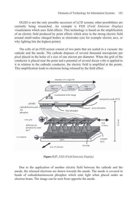
Elements of Technology for Information Systems 183
OLED is not the only possible successor of LCD screens; other possibilities are currently being researched. An example is FED (Field Emission Display) visualization which uses field effects. This technology is based on the amplification of an electric field produced by point effects which arise in the strong electric field around small-radius charged bodies or electrodes (see for example electric arcs, or why lighting hits the highest points).
The cells of an FED screen consist of two parts that are sealed in a vacuum: the cathode and the anode. The cathode disposes of several thousand micropoints per pixel placed in the holes of a size of one micron per diameter. When the grid of the conductor is placed near the point and a potential of several dozen volts is applied to it in relation to the cathodic conductor, the electric field is amplified at the points. This amplification leads to electrons being released by the field effect.
Figure 5.17. FED (Field Emission Display)
Due to the application of another electric field between the cathode and the anode, the released electrons are drawn towards the anode. The anode is covered in beads of cathodoluminescent phosphor which emit light when placed under an electron beam. The image can be seen from opposite the anode.

184 Nanocomputers and Swarm Intelligence
The development of FEDs will never use microtip technology. Due to their small size (1 to 2 mm), they cannot be produced on a large scale and can therefore not be exploited cheaply. Releasing electrons by carbon nanotubes which would allow the potential required to be decreased for emission could be a possible alternative when it comes to industrial applications. Motorola abandoned its research in the field of microtips in 2001 and is now investigating the electronic emission of nanotubes.
In 1986, the first monochromic screen-based on FED technology was presented by a team from LETI (Laboratory for Electronics and Information Technology). This team worked with an industrial partner called Pixtech to develop the production and the characteristics of FED screens. However, their research could not be exploited on a commercial level. Today, it is too early to say whether FED is a competitor to OLED screens. However, OLED screens will be used over the next 10 years and are LCD’s successor in this field.
5.5. Telecommunications – a different kind of revolution
Until quite recently, the telephone was the only means of telecommunication between two people. From the 1970s onwards computers increasingly used this infrastructure to exchange data. The exchange of information requires a much higher speed of transmission than the simple transport of a voice in a telephone network. The capacities of our networks needed to be increased on a very broad scale.
The world of telecommunications changed drastically at the end of the 1990s when the circulation of data exceeded that of the voice. The operators reformed their infrastructures to offer their clients ever more integrated services. The development of computers is therefore strongly linked to developments in telecommunications.
New infrastructures use digital networks and rely on the circulation of packets of information. Until the 1990s, telecommunication networks worked in analog mode. In other words, if a car wanted to go from city A to city B, the entire road between the two cities needed to be blocked for the time of the journey.
On the other hand, the circulation of packets of information allows several vehicles to use the street at the same time. The deregulation of the telecommunications market, and more particularly of the local loop (also referred to as a subscriber line) has largely accelerated the development of networks which offer several services at the same time.
The general user could estimate the progress made in the field of computers while developments in the field of telecommunications were unpredictable. However, with telecommunications via satellite, the improvement in laser

Elements of Technology for Information Systems 185
technology and the progress in the field of fiber optics, which has rapidly taken over from copper, the telecommunications industry is blossoming.
This trend will lead to important changes in telecommunications once a global movement of deregulation sets in and paves the way for competition on the market and the increasing popularity of the Internet. The Internet with its Internet Protocol (IP) can simultaneously diffuse all forms of communication. A packet of information can carry voice as well as image. Web solutions will unleash the imagination of providers in terms of content as well as service and will also change consumers’ habits.
From its invention onwards, the price of telecommunications remained rather stable. However, there has been a significant drop in the price over the last 10 years. All fields of telecommunications such as voice, data or video have become very cheap. Even video conferences, which were previously reserved to very large companies, have now made their way into general households.
The next step in this revolution which will favor the development of ambient intelligence and diffuse informatics is based on wireless connections. This new technology and the protocols that are used are playing a crucial role in the development of emerging platforms (see section 4.3.2) and third generation (3G) mobile telephones. These cell phones allow for an extremely high speed of information exchange. Telecommunications play a central role in the development of web diffusion.
The future of telecommunications lies in its network which could consist simply of nodes in the form of terminals. These nodes are the terminals themselves (cell phones, PDAs, laptops, etc.) which manage themselves and could replace stable antennae.
This analog principle called P2P (see section 4.3.3) is perfectly adapted to the introduction of a highly interlinked network in which the objects that communicate become omnipresent. The basic idea is the same as the one that gave rise to the ARPANET6 network. What would happen if the antennae were damaged by a natural disaster? 6 In the 1960s, the United States Department of Defense (DoD) commissioned a study on the reliability of communication networks during armed conflict. The famous and worrying report was given by the RAND Corporation, which is why this document is known as the “Rand Report”. The report stated that the communication infrastructure is extremely centralized and lacks autonomy of nodes which could take over in case a connection is cut between some of those points. If a secondary structure failed to provide its service, it could endanger the entire system. In the case of even a small nuclear attack the entire telecommunications network of the USA would be at risk. This report led to the creation of the ARPANET network, the

186 Nanocomputers and Swarm Intelligence
This danger could be avoided if mobile terminals serve as antennae within the network. The link is therefore made directly between two terminals that would like to communicate with each other. The solution also seems very convincing because stable antennae that cause permanent magnetic smog, and are therefore a danger to the public, would no longer be needed.
Even if this system seems very convincing, due to the absence of a central unit (i.e. swarm intelligence; see section 6.4.2), several problems are still linked to it. These are, for example, the confidentiality of the transmitted information, its quality, as well as the speed at which information can be transferred.
It will still take three to five years for these networks to be made available. However, a good knowledge of the density of these nodes is currently being established.
A system that manages itself can only be created if security can be guaranteed. In current networks, the protection of privacy and personal data protection are directly ensured by the provider. A self-organized network would no longer have such central control.
The nodes would directly exchange their digital security codes and their addresses. In order to do so, the nodes, or rather terminals7, need to be connected directly at least once to exchange their digital security codes and their addresses. This is the coupling process. This direct link would mean that the users of the terminals “know each other”. Terminals A and B “know each other” and can establish a secure connection. Their communication cannot be intercepted. If B knows the digital security code and the address of C, A can contact C via B without C knowing all security codes.
For a long time people believed that the danger for the security of independent networks lay in weak links within it. Simulations, however, have shown the opposite. This type of peer-to-peer relation could actually increase security.
predecessor to the Internet that is based on the following principles: tested and disposable equipment, shared connections, costs shared between the operators and field extensions. 7 In the short term, devices (e.g. objects or web services which indicate their properties and allow for them to be used) will show their methods online and allow other devices to check and manipulate them.
Elements of Technology for Information Systems 187
5.6. The triumph of microsystems
MEMS are made up of components between 10 to 100 microns in size (i.e. 0.1 to 0.01 mm). They usually consist of a central unit that processes data, the microprocessor and several components that interact with the outside such as microsensors for pressure, temperature, chemical or magnetic changes as well as one or more microactuators. Microsysems need to fulfill highly contradictory standards. They need to offer best performance at the lowest cost and with the least overload of data.
The first application that could be could be considered as a MEMS was a field effect transistor with a wired grid that was created by Westinghouse in 1969, a product that turned out to be more of an object of curiosity than something that could be exploited industrially. However, it still marks the beginning of this technology. At the beginning of the 1970s, the producers used engraved substrate plates to produce pressure sensors. At the beginning of the 1980s, research had moved on and the technique of micro-manufacturing was used to create actuators made up of silicon polycrystalline used in the read heads of disks. At the end of the 1980s, the potential of MEMS was widely recognized and their applications increasingly entered the fields of microelectronics and biomedicine.
In the 1990s MEMS received special attention, especially from the USA and government agencies offered support for projects in this field. During this period, the Air Force Office of Scientific Research (AFOSR) strengthened their research into materials and DARPA created its foundry service in 1993. At the same time, the National Institute of Standards and Technology (NIST) offered support to private foundries which were working in the fields of MEMS or produced CMOS components.
At the end of the 1990s the MEMS device was globally produced industrially. Factories that produced MEMS were built by companies such as Bosch and Motorola. The US government is still very interested in MEMS and continues to subsidize agencies such as DARPA. Recently, a series of miniaturized systems were used in order to control the performances of a space shuttle sent out by NASA. These systems were used for navigation, detection, propulsion, digitalization of data as well as to control temperature.
These systems that emerged more than 30 years ago have been omnipresent in our lives since the 1990s. They can be found in ABS systems, computer applications such as ink jet printing cartridges, all every day multimedia applications, cardiac pacemakers, and in the field of biology where lab-on-a-chip applications allow tests to be carried out, inside the target organism which avoids high costs.

188 Nanocomputers and Swarm Intelligence
In the 21st century, microsystems are mostly used in cars. A luxury car in 2003 contained as many electronics as an Airbus A310 did in the 1980s. In 1974, 4% of a car’s price represented the electronics used in it while in 2003 this figure increased up to 20%. In 2010 the estimated percentage will reach 35%.
Microsystems in the car industry have developed a great deal from their starting point, which was the “intelligent” pressure sensor for tires. MEMS are now a vital part of car systems and fulfill all different kinds of functions such as the accelerometer for airbags, sensor for petrol, controlling the breaking process and, last but not least, reducing the noise in the passenger compartment. Part of the latest innovation is “intelligent” tires that indicate to the driver if one of the tires is going flat. Their performance is so sophisticated that they are able to provide this information up to 80 kilometers before the tire eventually needs to be replaced.
Many other sectors also need to be mentioned here. Especially in the field of telecommunications, microsystems are used on very widespread hyperfrequencies. In the field of cell phones and satellite connections, optical microsystems are used for the optoelectronic conversion.
The fields of aeronautics, space travel and military, which first used microsystems, are still developing new projects. There is no need to give a list of all applications. Let us simply mention the micropyrotechnical systems which pave the way for applications such as microsatellites which weigh about 20 kg. Another interesting example is the research project that is trying to replace the flaps on airplane wings with a network of microflaps (similar to the feathers of a bird) in order to increase the performance in terms of security and fuel consumption.
Microsystems are currently undergoing strong industrial development and represent a market of €50 billion. Their growth rate lies at 15% per year for the last 10 years. This is a market that will grow even more as the production of microsystems will multiply tenfold in the next decade.

Elements of Technology for Information Systems 189
Microsystems growth forecasts
Biometric sensors market CAGR 1999-2005 40%
Lab-on-chip (LOC) sales CAGR 2002-2008 33%
LOC detection of biological/chemical agents market CAGR 1999-2004 20%
Microfluidic device sales annual growth 2002-2008 30%
Biochips US market annual growth 2002-2006 23%
Biomedical microsystems global market annual growth 2001-2011 20%
Medical applications using semi-conductors market annual growth 2004-2009
18%
Fiber optic component assembly/test products sales annual growth 2000-2005
21%
Source: Canadian Microelectronics Corporation, annual report 2004
Table 5.1. Outlook on the growth of microsystems
There are two main reasons that explain their commercial success and positive predictions for their future development. First of all, MEMS have shown reliable performance under extreme conditions and within extremely hostile environments (e.g. thermal shocks, extreme pressure, humid or salty environments, etc.). This fact makes MEMS an ideal candidate for all possible applications in different fields. The second reason for their success is that MEMS can be used for the mass market (e.g. car industry, telecommunications, household appliances, audio and video application, etc.). Therefore, their production is financially beneficial as is the creation of new applications.
The real challenge of these devices lies, however, in the rise of interconnected microsystems that are able to interact with one another, just like a colony of tiny intelligent objects. A new era of information systems has begun. In the past, the data processing units were centralized just like the brain of a primate. Now, the distribution of intelligence will move through the entire network. The diffusion of this decision-making power paves the way for four brilliant principles. These are increased calculating capacities, reactivity towards local situations, a tolerance towards problems (see section 5.5) and self-adaptation.

190 Nanocomputers and Swarm Intelligence
In 1991, Goss and Deneubourg showed in a simulation how a group of simple robots, which could represent a colony of microsystems working in a network, manage to navigate in an unknown space without a map, visual recognition, or the slightest point of orientation. The robots perceive the given space as smaller than it actually is and can encounter obstacles. However, these robots are able to collect objects which are scattered on a square surface and move them to the center of the space.
Even if the method of using colonies is currently less efficient than complex centralized systems, it beats all other competitors when it comes to simplicity, reliability and flexibility (adaptability).
5.7. Is this the end of the silicon era?
The question of whether the domain of silicon will finally reach its limits in the near future (i.e. 5 to 10 years) is far from being answered. This book does not aim to enter the Manichean debate of experts but would like to show that this domain could be combined with, and even benefit from, new trends in technology. More precisely, how can the value chain reorganize itself, open up opportunities and break the deadlocks that go hand in hand with these opportunities?
The debate on whether silicon will be a pillar of nanotechnology is similar to discussing what came first, the egg or the chicken. The term nanotechnology usually refers to processes, structures, materials and devices which are smaller than 100 nanometers. This term is used no matter whether traditional top-down processes or bottom-up assemblies are referred to. The controversy on this issue is brought about by the “purists” who base their ideas on a neologism under which only the second approach i.e. self-assembly and structures on an atomic scale are acceptable.
There is, however, a limit of quantum phenomena which will sooner or later come into force when traditional processes are used to work on a scale less than 50 nm. Since 1900, and mainly thanks to the research carried out by Max Planck, it has been known that energetic exchanges i.e. heat, electric current, light, etc. can only be carried out in small packets of elementary particles, the quanta, when working on a nanoscopic level.
Even if quantum phenomena are barely controlled and understood in the scientific and industrial sector, they still have a positive impact on certain devices that are currently used.

Elements of Technology for Information Systems 191
Since 2006, major companies that dominate, and therefore often limit the market of traditional microelectronics (Intel, Texas Instruments, AMD, etc.) have started working on the engraving process at 45 nm. This means that there are more than 20 million transistors positioned per meter. Only seven years ago experts considered such a high level of integration impossible.
At this level of miniaturization the devices are comparable to the size of a virus, they are therefore smaller than living organisms. Some layers of the material used are even slimmer than a virus. The new generation of transistors made from silicon oxide is only five molecules thick. We have, therefore, finally entered the domain of nanotechnologies. In other words, a domain where measuring units are on an atomic scale.
Over the course of 30 years the semi-conductor industry has greatly evolved. The amount of money spent in R&D facilities is higher than ever before and exceeds the money invested in the Apollo program that led to the landing on the moon. This figure currently makes up 15% of the turnover in the sector which is between €22 and €30 billion per year. In less than 15 years the three biggest European producers have multiplied their investment tenfold and have forced out an increasing number of players in this industry (see section 2.3.1).
During this period, this domain and the computer industry have profoundly reformed their value chain. What is usually called the “golden age of information technology” and marked by the arrival of the PC on the market also marks the beginning of a transition in organization. The trend moves from a vertical integration which is dominated by a handful of multinational players towards an economic distribution chain marked by a large network of companies which co-operate with one another. One form of co-operation is based on a traditional hierarchical relationship of sub-contractors who then work together as a form of strategic co-operation such as partnerships, consortiums, joint-ventures and other agreements made in technical sales. Everybody does business with everyone else, but even a commercial co-operation does not mean that those companies get along well.
After the new trend was introduced by the arrival of the PC, the emergence of open systems such as UNIX and the first standards that were set in terms of creating open systems has led to all partners being focused on a shared objective.
The reorganization process of medium and large size companies was perceived as progress in information systems by clients at the time. Vertical integration enabled technical directors and managing directors to relax. Companies such as IBM, DEC, Siemens, ICL and Bull were in charge of all technologies, produced all

192 Nanocomputers and Swarm Intelligence
devices from processors to programs and even added maintenance devices to their systems. The price was rather stable since there was not much competition on the market.
The new value chain that is currently emerging around open systems is questionable in terms of global responsibility as well as in terms of quality. On this note, the new value chain cannot compete with the previous system that was dominated by large companies. However, this new trend has opened up new segments in the market. These are the creation of small companies and a strong increase in usage. Information technology has entered the period of democratization. Parts of the economy might eventually by recovered by bigger companies which would eventually lead to a change in the criteria of profitability of the investment made in the field of information systems. Furthermore, this open value chain based on a virtual network of companies is extremely flexible and has adapted itself perfectly to the fluctuations of a market which has become more and more difficult to enter.
Between 1999 and 2000, the benefits of virtual value chains and of companies that co-operate were mainly seen as a product of the Internet.
These approaches require a system of organization as well as a communication tool that allows for co-operation. The Internet was therefore the ideal channel to be used. Otherwise, it would not make sense to outsource part of a company if the delivery of a quality product according to the deadline can no longer be guaranteed.
In fact, the concept of meta-companies had been introduced by much older systems of information exchange. In the 1950s, they were discreetly introduced in the car industry and in aeronautics. They were based on exchanges of documents printed in a structured manner. In the 1980s, the progress of viewdata and the exchange of data called EDI and EDIFACT standards further improved the situation.
Western car producers realized that Japanese companies were making great progress. Before it was too late they understood the secret which lay in the rapid and efficient communication with the sub-contractors and could therefore take action. The ODETTE organization that worked on the electronic exchange of data in the European car industry from the mid-1980s onwards can be considered as the first European meta-company.
Will the next step in technology erase the limits of information technology that are set by quantum phenomena? Will this be the beginning of electronics in molecular dimensions? Maybe the next step will not erase those limits straight away.

Elements of Technology for Information Systems 193
A report which was established by the Rand Corporation has investigated the interlinking of three key areas of technological research and development by 2015. These key areas are nanotechnologies, new materials and biology.
Taking into account the unification process of these scientific disciplines and the increasing transversality between them, the report showed that microsystems will play an important role. They use a traditional form of technology but distribute the computing power throughout the entire network. The technology basically remains the same but new applications will lead to visible changes.
At the same time, the first devices using nanotechnologies which are in extremely early stages of research will progressively be introduced into different applications in the next 15 years.
In other words, the development that is perceived by the user will be shown once more by the nature of its applications (i.e. dilution of microsystems) rather than by the technology itself. Nanotechnologies will go hand in hand with the trend towards spreading calculating power throughout the entire network which will mark the “new information technologies”.
Figure 5.18. Innovation, growth and level of pervasive systems, periodic cycles
The end of the silicon cycle does not symbolize a rupture. Rather, there will be a gradually increasing crossover between technologies similar to the phenomenon of the development from vacuum tubes to semi-conductors in the 1970s, or the development from the logical wired machines towards a digital technology that was micro-coded in the 1980s.

194 Nanocomputers and Swarm Intelligence
During this period, the user observed the change from black and white to color TV and discovered other digital devices such as teletext. However, the question of whether a TV is based on vacuum tubes, transistors or is equipped with a microprocessor leaves the user rather indifferent.
A realistic outlook shows that silicon will dominate the market for another 12 years. This decade will allow applications using nanotechnologies to emerge on an industrial scale and will leave time to resolve problems such as the assembly of a large number of very small objects.
Until then, the semi-conductor industry will rely on an extremely competitive production system in terms of cost and mass production of the components. They own the monopoly of an industrial process that has reached its final stage.
Figure 5.19. The assembly of a large number of very small devices can only be carried out in the field of silicon. In the short term, building plans for computers and the infrastructure of
information systems do not have an alternative to the domain of traditional semi-conductors (source STM)

Elements of Technology for Information Systems 195
The beginning of the nanotechnology industrial cycle will concentrate on high performance components while the silicon industry will continue to produce peripheral components. The production process will run at an optimal level and lead to an extremely high cost efficiency.
These changes in technology do not necessarily lead to changes in the players involved. The silicon domain is one of the industries that has been most commercialized throughout history. However, it also remains an example that can be applied to other fields. Because of their financial resources in the field of research and development, the companies which are focusing on silicon right now might be the first ones to propose industrial applications for nanotechnologies. IBM or Intel, amongst other companies previously mentioned, have shown that they are the forerunners in this field. Before entering the era of the quantum computer there are still many different aspects to be researched and exploited. In this way, it will be possible to push the limits set out by Moore’s Law even further and also reduce the cost for the production of a single device.
The real challenge for nanotechnologies compared to traditional photolithography on silicon lies in the aim to industrially produce logic gates of 20 nm or smaller in the next 12 to 15 years. The integration should be at more than 10 billion transistors per chip, which can be compared to assembling 10 billion bristles on a synthetic soccer pitch. Miniaturization also leads to an increased speed in operations. Several hundred thousand electrons were previously necessary to change one logic gate from “0” to “1”. Nanotechnologies only use one single electron or only a few electrons to carry out this change. With an increased speed and a reduced energy consumption, the work cycle of those new generations of machines will be more than 100 GHz as opposed to today’s 3 to 4 GHz. As the work cycle is directly linked to the heat that is produced during operations, the transfer of the charge of hundreds of billions of electrons per operation would melt a traditional silicon chip. The work cycle could not be higher than several GHz, at least for industrial applications.