nanobonding: a key technology for emerging applications …mrhowlader/publications... ·...
TRANSCRIPT

Nanobonding: A key technology for emerging applications
in health and environmental sciences
Matiar M. R. Howlader1, M. Jamal Deen1,2, and Tadatomo Suga3
1Department of Electrical and Computer Engineering, McMaster University, Hamilton, ON L8S 4K1, Canada2Electronic and Computer Engineering Department, The Hong Kong University of Science and Technology, Clear Water Bay, Kowloon, Hong Kong3Department of Precision Engineering, School of Engineering, The University of Tokyo, Bunkyo, Tokyo 113-8656, JapanE-mail: [email protected]; [email protected]; [email protected]
Received August 8, 2014; accepted October 25, 2014; published online January 29, 2015
In this paper, surface-activation-based nanobonding technology and its applications are described. This bonding technology allows for the inte-gration of electronic, photonic, fluidic and mechanical components into small form-factor systems for emerging sensing and imaging applications inhealth and environmental sciences. Here, we describe four different nanobonding techniques that have been used for the integration of varioussubstrates— silicon, gallium arsenide, glass, and gold. We use these substrates to create electronic (silicon), photonic (silicon and galliumarsenide), microelectromechanical (glass and silicon), and fluidic (silicon and glass) components for biosensing and bioimaging systems beingdeveloped. Our nanobonding technologies provide void-free, strong, and nanometer scale bonding at room temperature or at low temperatures(<200 °C), and do not require chemicals, adhesives, or high external pressure. The interfaces of the nanobonded materials in ultra-high vacuumand in air correspond to covalent bonds, and hydrogen or hydroxyl bonds, respectively. © 2015 The Japan Society of Applied Physics
1. Introduction
Integration, bonding and interconnection of components onheterogeneous substrates have been recognized as a powerfultechnology to create miniaturized, low-cost, and high sensi-tivity biomedical- and environmental-sensing and -imagingsystems.1) In this technology, system-on-chip, system-in-package, and system-on-package techniques are being utilizedto integrate more functions than that in Moore’s Law.2) Thisapproach is known as “More-than-Moore” (MtM) (Fig. 1).3)
The MtM approach allows for integrating electrical, optical,photonic, mechanical and fluidic devices for more functionalor smart sensing and imaging systems.4) At present, commonlyused integration technologies such as thermal compressionbonding,5,6) fusion bonding,7) plasma bonding,8,9) and adhe-sive bonding,10) require high pressure,5) elevated temper-atures,7) or chemical solvents.10,11) However, for sensing andimaging applications, some major challenges for the inte-gration of electronic, photonic, fluidic and dielectric materialsand devices are related to incompatibilities in the size (thick-ness and surface roughness),12) structure (crystal, amorphous,polycrystalline, orientation),13) plasticity (deformation),5,7)
chemical reactivity (hydrophilicity and hydrophobicity),8–11)
and thermal stability14) of the various components.The surface smoothness of electronic (silicon) and pho-
tonic (silicon, germanium and gallium arsenide) materials isbetter than that of microelectromechanical (glass) and fluidic(glass and polymers) materials. However, the plasticity of thelater group of materials is higher than that of the former.15–18)
These characteristics result in difficulties in integratingelectronic and photonic materials when an external force isrequired. Also, while the thermal stability of the electronicand photonic materials is considerably higher than that ofpolymers, the lattice mismatch and structure of electronic andphotonic materials is crucial when integrating them. Also,mismatches in the coefficients of thermal expansion areproblematic when heating is required in the integrationprocess. Furthermore, chemical reactivity of the surface is afunction of surface morphology and bonding atmosphere,which determines bonding spontaneity in the integration. Infact, the commonly used integration technologies mentioned
above (such as thermal compression, fusion, or plasmabonding) do not provide the required (1) high bond strength,(2) high electrical conductivity, (3) hermetic sealing, (4) sub-micrometer alignment accuracy, and (5) optical transparencyof the bonded interface between device and substrate withoutdegrading the performance of individual components in thebiosensing and bioimaging systems.
In this paper, we review some of the more promisingnanobonding technologies, especially those that can be usedin creating sensing and imaging systems for health andenvironmental applications. In Sect. 2, we describe some ofthe popular bonding methods. In Sect. 3, we briefly introducetwo examples of biosensing and bioimaging systems. InSect. 4, we describe some important aspects of samplepreparation and characterization. Section 5 contains someselected nanobonding results and discussions of some keyfeatures of nanobonded systems of materials. Finally, thesummary and future perspectives are presented in Sect. 6.
Fig. 1. (Color online) MtM for heterogeneous integration using surfaceactivated nanobonding.3)
Japanese Journal of Applied Physics 54, 030201 (2015)
http://dx.doi.org/10.7567/JJAP.54.030201
SELECTED TOPICS IN APPLIED PHYSICSAdvances in Low-Temperature Bonding Technologies for 3D Integration
030201-1 © 2015 The Japan Society of Applied Physics

2. Nanobonding methods
Nanobonding is a direct bonding technology based on surfaceactivation. It has capabilities for the integration of diversematerials with improved quality of interface19) being devel-oped for compact biosensing and bioimaging systems. Ananobonding technology refers to bonding of smooth sur-faces of similar or dissimilar materials. This technologyoffers nanometer-scale bonding at lateral dimensions in anultrahigh vacuum (UHV), or in air at room temperature.19,20)
Nanobonding can be classified into four categories. Table Isummarizes the categories of the nanobonding. In the firstapproach (direct adhesion), the mating surfaces are cleanedwith an argon fast atom beam (Ar-FAB), and direct adhesionoccurs when they are contacted in UHV.19–32) In the secondapproach (nano-layers adhesion), the surface cleaning andnano-adhesion layer deposition are simultaneously accom-plished using an Ar ion source followed by contact inUHV.33–36) In the third approach (sequential plasma activa-tion), the surfaces are cleaned by a radio-frequency (RF)reactive ion etching (RIE) plasma and microwave (MW)neutral radicals at low vacuum and then bonded in air.37–41)
In all three approaches, the cleaned surfaces are called theactivated surfaces.
The second and third approaches have been developed forionic materials to minimize their surface activation inducedpolarization effect. In the fourth approach (hybrid adhesion),the bonded wafers in the third approach are treated withthe anodic bonding method, that is, a voltage is appliedon the bonded wafers during heating at low temperature,in air.15,16,42) Compared with other existing direct bondingtechnologies,43,44) the advantages of the nanobonding tech-nology45) are the following.(1) Bonding dissimilar materials over wide areas with high
bond strength.(2) No requirement of applying external pressure, adhesive,
heat, or chemicals.(3) Sub-micrometer alignment accuracy.(4) Biologically compatible (i.e., non-toxic) interface.(5) Preserves delicate components and biological speci-
mens.
(6) Mechanical, electrical, and optical connections on thesame surface.
These properties are highly beneficial in bonding andintegrating devices from heterogeneous technologies.
High bonding strength offers enhanced tolerance of han-dling such as grinding and polishing during the fabricationand integration of structures and devices for sensing andimaging systems.45) Submicrometer alignment accuracyenables the integration of nanostructures and devices inmicro- and nano-systems. Optical transparency of the bondedmaterials controls transmitted optical signals,46) which arecritical for the analysis of chemical or biological species inoptical sensing systems. Another example of optical trans-parency is for the solar cells applications. The opticallytransparent material decreases the light reflection at theinterface, allowing photons to efficiently travel throughsubcells, thus enhancing the performance of the subcells.The improved electrical connection between the materialsreduces parasitic losses at the interface, resulting in enhancedcurrent flow. Therefore, nanobonding technology is a highlypromising technology for combining dissimilar materials,devices or components.
Nanobonding technology has been demonstrated in theintegration of diverse materials with different sizes andthicknesses.19,21–28,30–41) In this article, we discuss some ofour recent research results in direct bonding of a variety ofsubstrates including silicon, gallium arsenide, copper, goldand glass. We describe results from nanobonding using thefirst approach (direct adhesion in UHV) and the fourthapproach (the third approach followed by electrostatictreatment in air).
3. Biosensors, bioimagers and nanobondingrequirements
In this section, we provide two examples of systems beingdeveloped for emerging applications in health and environ-mental sciences. Very briefly, as shown in Fig. 2,47) in thisbiosensing system, a real world liquid sample such as blood,saliva from a human or water from a river or lake, is pumpedinto the filtration and concentration microelectromechanicalsystems (MEMS) module. The processed sample is then
Table I. Categories of surface activated nanobonding.
Type
Activation Bonding
MaterialsSource Gas Ambient Temperature Ambient
Applied
Voltage(kV)
Load(MPa)
Direct adhesion FAB Ar UHV RT UHV 0
³0.1–0.2
Si/Si,19,21,22) Si/SiO2,23) Si/GaAs,24) Si/InP,25)
GaAs/GaP,26) Cu/Cu,27,28) Au/Cu,30) Au/Al,30)
Al/Stainless steel,31) Sn–Ag–Cu solders32)
Nano-layersadhesion
LEI Ar UHV RT UHVSi/Si,33) Si/SiN,33)
Si/LiNbO3,34,35) Si/LiTaO336)
Sequential plasmaactivation
RF-RIE+
MW-NRsO2, N2 LV RT CRA 0
Si/Si,38,39) Si/glass,40) glass/glass,41)
Si/SiO2,83) Ge/SiO283)
Hybrid adhesion(SPA+electrostatic)
RF-RIE+
MW-NRsO2, N2 LV 150–200 °C CRA 1
Si/glass,15) Ge/glass,16)
GaAs/glass42)
SPA: sequential plasma activation. FAB: fast atom beam. LEI: low energy ion. RF-RIE: radio-frequency-reactive ion etching. MW-NRs: microwave neutralradicals. UHV: ultra-high vacuum. LV: low-vacuum. RT: room temperature. CRA: clean room air.
Jpn. J. Appl. Phys. 54, 030201 (2015) SELECTED TOPICS IN APPLIED PHYSICS
030201-2 © 2015 The Japan Society of Applied Physics

inserted into the cell processing module where the cells areextracted. Next, the cells are broken apart, nuclear DNAextracted and chemically processed to provide the requiredoligonucleotide related to the pathogen to be detected, andthen amplified.48–52) The double-stranded DNA is thendenatured to provide single-stranded (SS) oligonucleotideswhich are then pumped into a microfluidic channel53) to theBioFET sensors. The BioFETs were previously functional-ized with the matching SS oligonucleotide for possiblehybridization. If the pathogen to be sensed is present in theprocessed real-world sample, then hybridization occurs,which are then sensed by the BioFETs.
As shown, the biosensing system includes control, signalconditioning and signal processing electronics54–57) toimprove the quality of sensed signal. It also includes a low-power, low-cost silicon-based wireless transceiver58–62) tosend information from the sensing environment (e.g., a ruralarea) to an urban center where appropriate actions can betaken if pathogens are present in the water sample. As shown,different material systems such as glass, various types ofpolymers, metals, silicon, gallium arsenide or indium phos-phide are required to be bonded onto a common substrate.The nanobonding technologies discussed above is beingdeveloped for applications such as this and the one im-mediately below in Fig. 3 for bioimaging. More details onvarious components of this biosensing system can be foundin our previous articles.45,47,63–65)
Figure 3 shows an optical bioimaging system that is beingdeveloped to detect autofluorescent signatures from tis-sues,64,65) for example. One application we are pursuing isautofluorescence spectral and lifetime signatures of tissuesfrom the gastrointestinal tract during a normal endoscopicor colonoscopic examination. These signatures, whenmatched to templates in a database, can be a screening anddiagnostic tool for early detection of diseases. We havealready developed compact concave gratings for spectralwavelength separation and focusing,66,67) several typeshigh-speed, high-sensitivity photodiodes and imagers67–75)
and optical coupling systems.74,75) We have also devel-oped data and signal processing electronics.54–57) Theseindividual components or systems, together with othersbeing developed (such as lasers, and antennas), in diversetechnologies (silicon, GaAs, InP, glass or polymer, etc.) mustbe integrated and bonded to create compact, high-perform-ance bioimaging systems.67,74–79) It is such technologiesthat nanobonding technologies are expected to play a criticalrole. In the next section, we provide details on the prepara-tion and characterization of samples from nanobondingexperiments.
4. Specimen preparation and characterization
As received wafers were used for the surface characterizationsand bonding experiments. No chemical treatments or process-ing were used, unless otherwise mentioned. For nanobonding,a number of custom designed bonders have been developedthat allow for bonding in UHV,19) low vacuum20) and air.15)
Before bonding, the contact angle and surface roughness ofthe non-activated and activated surfaces were investigated.The sessile drop method was used to determine the contactangle with a deionized (DI) water droplet (9 µL), using aKruss DSA100. The surface roughness was measured with anatomic force microscope (AFM) from Veeco (ICON). Forinterfacial characterization, the bonding strength, nanostruc-ture and current–voltage (I–V ) characteristics of the bondedinterfaces were examined. To measure the bonding strength, atensile pulling tester from Instron was used. Scanning electronmicroscope (SEM) and high resolution transmission mi-croscopy (HRTEM; JEOL JEM-2100F), were used to observethe micro- and nano-structure of the bonded interfaces. TheI–V characteristics were measured using a semiconductorparameter analyzer (HP-4145B). Most experiments werecarried out in the Micro- and Nano-Systems Laboratory(MNSL) at McMaster University.
Figures 4(a) and 4(b) show a typical example for the AFMimages of a Si surface before and after activation. Thesurfaces were homogeneously activated over the entire 2-in.diameter wafer by placing the activation sources at 45° withrespect to the center of the specimens.19) All the specimensfor nanobonding in UHV were activated with a 1.5 keVAr-FAB source using 48mA for 300 s, unless otherwisementioned. Smooth surfaces were observed before and afteractivation. While the root mean square (RMS) surfaceroughness of Si before activation was 0.17 nm, it decreasedto 0.11 nm after activation. Hence, the clean and smoothsurfaces, that are required for the nanobonding of diversewafers, were maintained or improved after activation.
5. Nanobonding results and discussion
5.1 Si/GaAsNanobonding in UHV requires thin wafers with low surface
Fig. 2. (Color online) Example of a biosensing system for the detection ofpathogens in water using DNA hybridization.
Fig. 3. (Color online) Example of a bioimaging system for the detectionof autofluorescence signatures for disease detection.
Jpn. J. Appl. Phys. 54, 030201 (2015) SELECTED TOPICS IN APPLIED PHYSICS
030201-3 © 2015 The Japan Society of Applied Physics

roughness. These parameters ensure intimate contact betweenthe wafers to be bonded. In general, optically mirror-polishedwafers provide nanometer-scale contact between the wafers.This intimate contact between two surfaces properly cleanedby using an Ar-fast atom beam in UHV can result inenhanced adhesion.
Figure 5(a) shows the infrared (IR) transmission images ofthe interfaces of Si/GaAs bonded using the nanobondingtechnology in UHV at room temperature.24) A number ofvoids were observed at the interfaces due to the presence ofparticles and other defects (e.g., metals ions) on the activatedsurfaces. The white and broken areas at the edges of theSi/GaAs bonded wafers are a result of the blade test. Theblade test was performed in order to measure the bondingstrength of the wafers. The insertion of the blade at thebonded interface failed due to the high bonding strength ofthe Si/GaAs substrates. Figure 5(b) shows the fracture imageof Si/GaAs interfaces after the tensile pulling test.24) Bulkfractured GaAs remained on Si. The bonding strength ofSi/GaAs was 14.4MPa. This behavior shows that thebonded interface is not debonded during or after polishing.In general, the bonding strength depends on the weaker waferof the bonded pair. Therefore, the relatively lower bondingstrength of Si/GaAs24) than that of Si/Si21) can be due to theweaker fracture strength of the GaAs bulk material.
Figure 5(c) shows the HRTEM image of the interface ofbonded Si/GaAs wafers.24) The thickness of the interfacialamorphous layer was 11.5 nm. The amorphous layer pro-duced was due to the distortion of the lattice sites of Siand GaAs by the current of Ar-FAB.17,21–25,27) This amor-phous layer is in contrast to that in the hydrophilic andhydrophobic bonding methods. The interfacial layer in thesemethods contains hydroxyl/oxide and hydrogen bonds, res-pectively.21,27,37) Therefore, the nanobonding in UHV is acovalent bonding rather than chemical reactivity of hydroxyl/oxide and hydrogen bonds in the hydrophilic and hydro-phobic bonding.21,27)
Figure 5(d) shows the I–V behavior of p-Si/n-GaAsbonded wafers. The resistivity of the p-Si and n-GaAs were(0.01–0.02) and (2.2–2.3) © 10¹3³0cm, respectively. Theelectrodes for Si and GaAs were made by deposition of Au
and Au/Ge with 3mm diameter before bonding for the ohmiccontacts. A non-typical I–V curve of the p–n junction wasobserved. However, analysis of the ideality factor of thejunction using thermionic emission theory showed that theideality factor of p-Si/n-GaAs was about 3.0.17,80) Theelectrical transport mechanism of Si/GaAs may be affectedby the interfacial amorphous layer between Si and GaAs. Theproperties of this interfacial layer are most likely determinedby the activation energy and time.17) The influence ofactivation parameters such as the Ar-FAB energy and activa-tion time on the current density of the p–n junction wasobserved, as well as the influence of the exposure time in theUHV atmosphere.17)
5.2 Ge/GaAsWe have reported heterogeneous semiconductor waferbonding of p-Ge/p-GaAs using nanobonding technology inUHV at room temperature.81) The dopants for Ge and GaAswafers were gallium and zinc, respectively. The doping con-centrations for both wafers were 1018 cm¹3. Surfaces ofGe and GaAs wafers with RMS roughness of 0.25 and0.48 nm,81) respectively, were simultaneously activated usingtwo Ar-FABs. The vacuum pressure of the chamber was³6 © 10¹6 Pa. The energy and current of the FAB was1.1 keV and 100mA, respectively. The activated wafersurfaces were contacted with an applied load of 1960N for2min at room temperature.
Figures 6(a) and 6(b) show the scanning acoustic micro-scope (SAM) images of the Ge/GaAs nanobonded interfacesbefore and after annealing, respectively. The annealing wasdone in nitrogen at 250 °C for 2 h. Before annealing, thebonded interface showed a number of voids. These voidswere annealed out.81) The mechanisms responsible for thebehavior of the interfacial voids before and after annealinghave not been studied in detail as yet. In fact, the SAM resultof the nanobonded Ge/GaAs interface is different from the
(a)
(b)
Fig. 4. (Color online) AFM images of Si surface (a) before and (b) aftersurface activation.21)
Fig. 5. (Color online) (a) IR transmission image (b) fracture image,(c) HRTEM image, and (d) I–V characteristics of the p-Si/n-GaAs bondedinterface. The specimens were bonded by using the nanobonding technologyin UHV at room temperature.24)
Jpn. J. Appl. Phys. 54, 030201 (2015) SELECTED TOPICS IN APPLIED PHYSICS
030201-4 © 2015 The Japan Society of Applied Physics
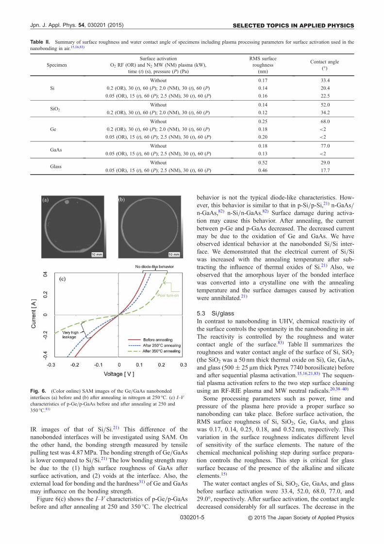
IR images of that of Si/Si.21) This difference of thenanobonded interfaces will be investigated using SAM. Onthe other hand, the bonding strength measured by tensilepulling test was 4.87MPa. The bonding strength of Ge/GaAsis lower compared to Si/Si.21) The low bonding strength maybe due to the (1) high surface roughness of GaAs aftersurface activation, and (2) voids at the interface. Also, theexternal load for bonding and the hardness31) of Ge and GaAsmay influence on the bonding strength.
Figure 6(c) shows the I–V characteristics of p-Ge/p-GaAsbefore and after annealing at 250 and 350 °C. The electrical
behavior is not the typical diode-like characteristics. How-ever, this behavior is similar to that in p-Si/p-Si,21) n-GaAs/n-GaAs,82) n-Si/n-GaAs.82) Surface damage during activa-tion may cause this behavior. After annealing, the currentbetween p-Ge and p-GaAs decreased. The decreased currentmay be due to the oxidation of Ge and GaAs. We haveobserved identical behavior at the nanobonded Si/Si inter-face. We demonstrated that the electrical current of Si/Siwas increased with the annealing temperature after sub-tracting the influence of thermal oxides of Si.21) Also, weobserved that the amorphous layer of the bonded interfacewas converted into a crystalline one with the annealingtemperature and the surface damages caused by activationwere annihilated.21)
5.3 Si/glassIn contrast to nanobonding in UHV, chemical reactivity ofthe surface controls the spontaneity in the nanobonding in air.The reactivity is controlled by the roughness and watercontact angle of the surface.83) Table II summarizes theroughness and water contact angle of the surface of Si, SiO2
(the SiO2 was a 50 nm thick thermal oxide on Si), Ge, GaAs,and glass (500 « 25 µm thick Pyrex 7740 borosilicate) beforeand after sequential plasma activation.15,16,21,83) The sequen-tial plasma activation refers to the two step surface cleaningusing an RF-RIE plasma and MW neutral radicals.20,38–40)
Some processing parameters such as power, time andpressure of the plasma here provide a proper surface sonanobonding can take place. Before surface activation, theRMS surface roughness of Si, SiO2, Ge, GaAs, and glasswas 0.17, 0.14, 0.25, 0.18, and 0.52 nm, respectively. Thisvariation in the surface roughness indicates different levelof sensitivity of the surface elements. The nature of thechemical mechanical polishing step during surface prepara-tion controls the roughness. This step is critical for glasssurface because of the presence of the alkaline and silicateelements.15)
The water contact angles of Si, SiO2, Ge, GaAs, and glassbefore surface activation were 33.4, 52.0, 68.0, 77.0, and29.0°, respectively. After surface activation, the contact angledecreased considerably for all surfaces. The decrease in the
Fig. 6. (Color online) SAM images of the Ge/GaAs nanobondedinterfaces (a) before and (b) after annealing in nitrogen at 250 °C. (c) I–Vcharacteristics of p-Ge/p-GaAs before and after annealing at 250 and350 °C.81)
Table II. Summary of surface roughness and water contact angle of specimens including plasma processing parameters for surface activation used in thenanobonding in air.15,16,83)
SpecimenSurface activation
O2 RF (OR) and N2 MW (NM) plasma (kW),time (t) (s), pressure (P) (Pa)
RMS surfaceroughness
(nm)
Contact angle(°)
Si
Without 0.17 33.4
0.2 (OR), 30 (t), 60 (P); 2.0 (NM), 30 (t), 60 (P) 0.14 20.4
0.05 (OR), 15 (t), 60 (P); 2.5 (NM), 30 (t), 60 (P) 0.16 22.5
SiO2Without 0.14 52.0
0.2 (OR), 30 (t), 60 (P); 2.0 (NM), 30 (t), 60 (P) 0.12 34.2
Ge
Without 0.25 68.0
0.2 (OR), 30 (t), 60 (P); 2.0 (NM), 30 (t), 60 (P) 0.18 <2
0.05 (OR), 15 (t), 60 (P); 2.5 (NM), 30 (t), 60 (P) 0.20 <2
GaAsWithout 0.18 77.0
0.05 (OR), 15 (t), 60 (P); 2.5 (NM), 30 (t), 60 (P) 0.13 <2
GlassWithout 0.52 29.0
0.05 (OR), 15 (t), 60 (P); 2.5 (NM), 30 (t), 60 (P) 0.46 17.7
Jpn. J. Appl. Phys. 54, 030201 (2015) SELECTED TOPICS IN APPLIED PHYSICS
030201-5 © 2015 The Japan Society of Applied Physics

contact angle increases the surface energy and therebyenhances the chemical reactivity of the surface.83) Thedecrease in the contact angle was significant for Ge and GaAssurfaces. The contact angle was less than 2° which is below thedetection limit of the DSA. This very low contact angle is dueto the termination of large amount of hydroxyl moleculeson the free-dangling sites of plasma cleaned Ge and GaAssurfaces when exposed to the clean room ambient.83)
However, a simple analytic relationship between the surfaceroughness and the contact angle was not observed.
Figure 7(a) shows the optical image of glass/Si wafersbonded by the sequential plasma activation followed byanodic bonding at 200 °C with the anodic voltage of 1 kV.15)
This process is known as hybrid plasma bonding (HPB).While the voids were observed at the interface in thesequential plasma activated bonding (SPAB), the void-freeinterfaces were achieved by using HPB. In HPB, voids wereabsorbed in the interfacial oxide.15) The absorption of thevoids depends on the thickness of the oxide. However, thevoids due to the presence of particles on the activated surfaceand plasma induced surface defects that trap air at theinterface could not be removed. Therefore, HPB provides anearly void-free interface by combining effect of electrostatic
force and adhesion between the hydrophilic surfaces.15,16)
Unfortunately, we have not yet investigated HPB for hydro-phobic surfaces. Figure 7(b) shows the fracture images ofbonded glass/Si wafers in SPAB and HPB after tensilepulling tests.15) The left image indicates a partial fracture ofglass in SPAB. The right image shows a complete fractureof glass after HPB at 200 °C. That is, while fractures atthe interface and bulk materials of Si and glass were observedin the SPAB, fractures only in the bulk material of glass wereobserved in the HPB. This indicates stronger bondingstrength in the HPB than that in the SPAB.15) Figure 7(c)shows the HRTEM images of the hybrid plasma bondedinterfaces of Si/glass.15) The HRTEM images show thepresence of intermediate amorphous layers at the bondedinterfaces. The thickness of the interfacial amorphous layerwas ³353 nm. The amorphous layer was brighter than bulkglass and Si, which was a sodium depletion region identifiedby using energy dispersive X-ray analysis.84) The higherbrightness was due to the smaller mean atomic number of thedepletion region compared to that of the bulk glass, causedby the migration of sodium and potassium cations.85) A darkband was observed at the interface of Si/glass. The dark bandat the edge of depletion region in glass was attributed to theaccumulation of less mobile potassium cations.85)
Figure 8 shows a comparative study of the bondingstrength of Si/Si, glass/glass, Si/Ge, SiO2/Ge, Si/glass,Ge/glass, and GaAs/glass bonded wafers with differentbonding conditions. The activation parameters for thespecimens are given in Table II. The activation parametersfor all the specimens are identical except the energy of O2
RIE plasma for the GaAs and Glass wafers. Also, the surfaceroughness of glass is higher than that of other wafers.Furthermore, while the water contact angles of Ge and GaAsbefore the activation are in the ranges of 70°, surfaceactivation changes them into the values that are below thedetection limit of the water contact angle measurementequipment (i.e., DSA100).
Substrates of Si/Si and glass/glass were bonded usingSPAB at room temperature.41,86) Si/Si and glass/glass werenot heated because heating does not improve the bondingstrength in SPAB due to the formation of voids at the bonded
Fig. 7. (Color online) Images of (a) optical (b) fracture and (c) HRTEM ofSi/glass interface bonded by hybrid plasma bonding at 200 °C and 1 kV for10min.15)
Fig. 8. (Color online) Bonding strength of Si/Si, glass/glass, Si/Ge,SiO2/Ge, Si/glass, Ge/glass, and GaAs/glass bonded wafers. The specimensof Si/Si and glass/glass were bonded by using the SPAB at roomtemperature. The specimens of Si/Ge and SiO2/Ge were bonded by usingthe SPAB and were heated at 200 °C for 4 h. The specimens of Si/glass,Ge/glass, and GaAs/glass were bonded by using hybrid plasma bonding at200 °C and 1 kV for 10min.15,16,41,83,86)
Jpn. J. Appl. Phys. 54, 030201 (2015) SELECTED TOPICS IN APPLIED PHYSICS
030201-6 © 2015 The Japan Society of Applied Physics

interface.21,41,86–88) The specimens of Si/Ge and SiO2/Gewere bonded by using SPAB and were heated at 200 °Cfor 4 h.83)
The specimens of Si/glass, Ge/glass, and GaAs/glasswere bonded by using HPB at 200 °C and 1 kV for 10min.15,16,83) The bonding strength of Si/glass is the highestcompared to all other wafers. This is as a result of highlyhydrophilic, reactive, and smooth surfaces of Si and glassafter sequential plasma activation. Si/Si and glass/glasswafers, after Si/glass, offer high bonding strength at roomtemperature. It is worth noting that while the Si and glasssurfaces have identical hydrophilicilty, that is the highreactivity and smooth surfaces in both the SPAB and HPBmethods, why the Si/glass bonded interface in HPB showsthe highest bonding strength. The highest bonding strength inHPB is due to the formation of an alkaline depletion layer inthe glass and an amorphous SiO2 interface that is shared bythe bonded wafers. These phenomena are attributed to theopposite migration of alkaline cations and anions between thecontacted wafers under the applied voltage at an elevatedtemperature.15,87,88) The bonded interface in SPAB doesnot provide to these phenomena21,41,86) that results in highbonding strength.
The bonding strength of Si/Ge was the lowest. This is dueto the high reactivity of Ge wafer after surface activation. Theactivated surface is terminated by hydroxyl molecules whenexposed to the clean room ambient. The hydroxyl moleculesresult in low water contact angle of less than 2° whichremains unchanged after 2min of the measurements. Thislow water contact angle indicates a large number of OH¹
molecules at the Ge activated interface. Therefore, the highreactivity is responsible for the weak bonding strength ofSi/Ge. After heating at 200 °C, the bonding strength ofSi/Ge was slightly improved, but this temperature was stillnot sufficient to remove the OH¹ molecules. Identical resultson the weak bonding strength of Si/Ge were reported89) dueto the enhanced surface oxidation induced by the oxygenand nitrogen radicals. The bonded wafers were annealedat 200 °C for 24 h, and additionally at 300 °C for 24 h toimprove the bonding strength.89)
The relatively high bonding strength of glass/Ge is due tothe increase in surface energy (i.e., low water contact angle)after surface activation38) of glass. Higher reactivity differ-ence of SiO2/Ge wafers is again due to the unique reactivityof Ge, as well as the water absorption of SiO2 layer.Annealing at 200 °C offers higher boding strength in SiO2/
Ge compared to that in Si/Ge. The bonding strength of Si/Geand SiO2/Ge in SPAB after annealing at 200 °C was lowerthan that of Si/Si and glass/glass in SPAB at room tem-perature. As previously mentioned, this relatively low bond-ing strength in the Si/Ge and SiO2/Ge can be attributed tothe high reactivity of activated Ge wafer after being exposedto air. This phenomenon is in contrast to that in the nano-bonding of Si/Si and glass/glass in UHV that results strongcovalent bonding at room temperature.15,16,21,83) In HPB,the difference in bonding strengths of Si/glass, Ge/glass,and GaAs/glass is due to the difference in the widths of thedepletion layer at the interface and the strengths of the bulkmaterials of Si, Ge, and GaAs wafers. Thicker depletion layerat the interface, and weaker strength of materials results inlower bonding strength and vice-versa.15,16,21,83)
5.4 Cu-through silicon vias/Au-stud bumpsThe copper-through silicon vias (Cu-TSVs) and gold-studbumps (Au-SBs) nanobonding was accomplished in UHVafter surface activation with a 1.5 keV Ar-FAB using 48mAfor 300 s at room temperature. While the Au-SBs have beenused in microelectronics packaging for a long time, high-density interconnection between Cu-TSVs and Au-SBsthrough nanobonding can be used in the miniaturizedbiosensing and bioimaging systems.45,90) The shape of thetop surface of stud bumps does not allow for nanobonding.Therefore, a low cost solution has been utilized to flatten thetop surface of the stud bumps by applying an externalcompressive pressure of about 81.5MPa over each bump(external force 0.16N/bump) on this surface.90) This processimproved the surface roughness and contact area thatrequired for the nanobonding.
The first three figures in Fig. 9 show the scanning elec-tron microscope images of the flattened Au-stud bumps[Fig. 9(a)]; the AFM images of Au-stud bump surfaceover 10 © 10 µm2 of deformed (flattened by using theexternal force) [Fig. 9(b)] and non-deformed (not-flattened)[Fig. 9(c)] areas, respectively. Figure 9(d) shows the opticalimage of Cu-TSV wafer and Fig. 9(e) shows the AFM imageof Cu-TSV surface over 10 © 10 µm2 of area. Figure 9(f )shows the optical image of the cross-section of Au-SB/Cu-TSV. The base and height of the Au-SBs were 50 and 37 µm,respectively. The Au-SBs were flattened using an external
Fig. 9. (Color online) (a) SEM images of the flattened Au-stud bumps;AFM images of Au-stud bump surface over 10 © 10µm2 of (b) deformedand (c) non-deformed areas; (d) optical image of Cu-TSV; (e) AFM image ofCu-TSV surface over 10 © 10µm2 of area; and (f ) cross-sectional opticalimage of vertically integrated Au-SB/Cu-TSV interfaces.90)
Jpn. J. Appl. Phys. 54, 030201 (2015) SELECTED TOPICS IN APPLIED PHYSICS
030201-7 © 2015 The Japan Society of Applied Physics

compressive pressure about 81.5MPa over each bump toimprove the surface roughness. A number of Cu-TSVs (120)were vertically sandwiched between two chips with Au-SBs.The RMS surface roughness of the deformed area was9.6 nm, which is significantly improved compared with thatof non-deformed area (36.1 nm). Through AFM investiga-tions of TSV surface over 10 © 10 µm2 of area in Fig. 9(e),the surface roughness was measured to be 6 nm. Since thissurface roughness of deformed Au-SBs and Cu-TSVs doesnot fully meet the requirement of nanobonding in UHV,19) a20N external force was applied for bonding at room tem-perature. The estimated applied pressure was about 81.5MPa(i.e., 0.16N/bump area). Here the base of the bumps (i.e.,50 µm) was used for the calculation of the bump area. Afterbonding, no considerable misalignment is observed in thecross-sectional view of the bonded Au stud bumps andCu-TSV, as shown in Fig. 9(f ). In addition, the bondingstrength of Au-SB and Cu-TSV was approximately as high as110MPa.90)
The electrical resistance of the interconnect, whichincludes two interfaces between Au-SB and Cu-TSV andthe height of one Cu-TSV, was only 0.5³.90) A mechanicalcaulking technique has been reported to bond Au-SBs withTSVs at room temperature to achieve three-dimensional (3D)assembly by applying compressive pressure to squeeze theformer into the latter.5) The compressive pressure is about815MPa,5) which is about one order higher than that of thepressure used in this work.90)
5.5 Chemical/vapor assisted nanobondingFurther modification in the surface preparation for nano-bonding has been realized in order to address the prolongedactivation time issue for some materials such as Cu. Ingeneral, a Cu surface contains 10–20 nm thick oxides. Thesurface activation of Cu using Ar-FAB for the nanobondingrequires prolonged etching time due to the thick oxides.29)
The prolonged activation results in a rough surface andcauses failure of Cu/Cu bonding in the UHV. Therefore, it isvery difficult to remove copper oxides and achieve highquality of nanobonding of Cu/Cu. On the other hand, theambient for surface activation of semiconductors, such as Siand GaAs is critical in the first category of nanobonding ifUHV is not maintained. Many of the combinations of thesemiconductors do not bond without UHV. To address theseissues, a new modified method of the nanobonding has beendeveloped.91–93) It is known as chemically assisted nano-bonding. In this method, the Cu surfaces were treated usingformic acid gas for surface activation. Formic acid gas wasgenerated using N2 gas bubbling through a bottle having asolution of formic acid. The treatment of Cu with formic gasreduces its oxide. The X-ray photoelectron spectroscopyspectra showed that 9min of formic acid gas activationcompletely removed hydroxide, oxides and organic contam-inations from the Cu surface.91,93) Therefore, the chemicallyassisted activated surfaces of Cu can be bonded at a tem-perature below 200 °C.91–93)
In another study, water vapor was used to bond variouscombinations of bumpless Cu structures, SiO2, and poly-imide.94) The motivation in this modified method is identicalto that in the third category of nanobonding. It is to createhydroxyl groups on the surface after activation. In the vapor-
assisted nanobonding,94) the smooth surfaces were activatedwith an Ar-FAB source using 1.5 kV and 15mA for 180 s,followed by exposure to the nitrogen atmosphere containingwater vapor of various absolute humidities for 600 s. Thepressure for exposing nitrogen gas was 9 © 104 Pa (0.89 atm).Cu surface was changed into Cu hydroxide. On the otherhand, the surfaces of SiO2 and polyimide were terminatedwith silanol and hydroxyl groups. Finally these surfaces weremated at RT and then heated at 150 °C for 600 s.94) The newlygrown and terminated layers resulted in strong adhesion afterheating. The bonded interface of Cu/Cu had an electricalresistivity of 4 © 10¹8³0m.94)
6. Conclusions and future perspectives
Four types of surface-activated nanobonding have beendeveloped to address the heterogeneous integration chal-lenges for “More than Moore”. The nanobonding techniquesoffer nanometer scale bonding through direct contactbetween smooth surfaces. Therefore surface preparation isone of the key parameters which control the quality of thebonded interface. The bonding quality is also dependent onthe sensitivity of the surfaces to activation source, bondingatmosphere and external force.
Nanobonding in ultrahigh vacuum (UHV) has beenperformed at room temperature for heterogeneous integra-tion of semiconductors, such as Si/GaAs, Ge/GaAs, andSi/glass. Void-free, strong, and atomic-scale bonding wasconfirmed. The I–V behavior of the nanobonded p–n junctionof the semiconductors was leaky. Investigation on controllingactivation parameters, such as voltage, current and powerof the sources is needed to achieve typical p–n junctionbehavior.
An example of nanobonding of metallic materials using Cuthrough silicon vias (Cu-TSV)/Au-stud bumps (Au-SBs) inUHV has been demonstrated. Cu-TSVs have been verticallyintegrated between chips with Au-SBs for 3D integrationat room temperature. High bond strength was identified atthe Cu/Au interface.
For nanobonding in air at room temperature, a sequentialplasma activated bonding (SPAB) technique has been devel-oped. The O2 RIE plasma followed by MW N2 radicals wasused for the sequential plasma activation. For nanobondingof ionic materials, the sequentially activated semiconductorsand glass were bonded under anodic treatment at 200 °C,known as the hybrid plasma bonding (HPB) technique. Void-free, strong and nanometer scale bonding of diverse materialsin HPB were observed.
Further modification in the surface preparation for nano-bonding was needed to address the activation challengesof surfaces with thick oxide, such as Cu surface. This newlymodified nanobonding utilizes chemical/vapor to ease thethick oxide issues. Prior to the activation of Cu surfaces,formic acid gas was used to reduce the Cu-oxide. Thesechemically assisted activated surfaces of Cu were bondedat 200 °C. Also, water vapor assisted different combinationsof bumpless Cu structures, SiO2, and polyimide were bondedat 150 °C. Therefore, the heterogeneous integration capabil-ities of the nanobonding technologies may have significantpotential and opportunities in the development of thebiosensing and bioimaging systems for emerging applicationsin health and environmental sciences.
Jpn. J. Appl. Phys. 54, 030201 (2015) SELECTED TOPICS IN APPLIED PHYSICS
030201-8 © 2015 The Japan Society of Applied Physics

Acknowledgments
This research is supported by Discovery Grants from theNatural Science and Engineering Research Council ofCanada, an infrastructure grant from the Canada Foundationfor Innovation, an Ontario Research Fund for ResearchExcellence Funding Grant, a FedDev of Southern Ontariogrant and the Canada Research Chair program.
1) International Technology Roadmap for Semiconductors (ITRS), 2007.2) R. R. Tummala, IEEE Spectrum 43, 44 (2006).3) More-than-Moore White Paper, International Technology Roadmap on
Semiconductors (ITRS), 2010.4) T. D. Wang and J. V. Dam, Clin. Gastroenterol. Hepatol. 2, 744 (2004).5) N. Tanaka, Y. Yoshimura, M. Kawashita, T. Uematsu, C. Miyazaki, N.
Toma, K. Hanada, M. Nakanishi, T. Naito, T. Kikuchi, and T. Akazawa,IEEE Trans. Adv. Packag. 32, 746 (2009).
6) S.-H. Choa, Microsyst. Technol. 15, 677 (2009).7) Y. T. Cheng, L. Lin, and K. Najafi, J. Microelectromech. Syst. 9, 3 (2000).8) K. Schjølberg-Henriksen, S. Moe, M. M. V. Taklo, P. Storås, and J. H.
Ulvensøen, Sens. Actuators A 142, 413 (2008).9) X. X. Zhang and J.-P. Raskin, J. Microelectromech. Syst. 14, 368 (2005).
10) S.-D. Song, S. L. Holl, C. Colinge, K. Y. Byun, K. D. Hobart, and F. Kub,ECS Trans. 16 [8], 287 (2008).
11) S. Lai, H. Lin, and C. Hu, Mater. Chem. Phys. 83, 265 (2004).12) V. Dragoi, G. Mittendorfer, C. Thanner, and P. Lindner, Microsyst. Technol.
14, 509 (2008).13) Z. R. Huang, D. Guidotti, L. Wan, Y.-J. Chang, J. Yu, J. Liu, H.-F. Kuo,
G.-K. Chang, F. Liu, and R. R. Tummala, IEEE Trans. Components Packag.Technol. 30, 708 (2007).
14) W. K. Jeung, C. H. Lim, J. Yuan, and S. W. Park, 2008 DTIP MEMSMOEMS, 2008, p. 201.
15) M. M. R. Howlader, M. G. Kibria, F. Zhang, and M. J. Kim, Talanta 82, 508(2010).
16) M. M. R. Howlader, M. G. Kibria, and F. Zhang, Mater. Lett. 64, 1532(2010).
17) M. M. R. Howlader, T. Watanabe, and T. Suga, J. Vac. Sci. Technol. B 19,2114 (2001).
18) M. M. R. Howlader, T. Suga, A. Takahashi, K. Saijo, S. Ozawa, and K.Nanbu, J. Mater. Sci. 40, 3177 (2005).
19) M. M. R. Howlader, A. Yamauchi, and T. Suga, J. Micromech. Microeng.21, 025009 (2011).
20) M. R. Howlader, H. Itoh, T. Suga, and M. Kim, ECS Trans. 3 [6], 191(2006).
21) M. M. R. Howlader and F. Zhang, Thin Solid Films 519, 804 (2010).22) H. Takagi, R. Maeda, N. Hosoda, and T. Suga, Jpn. J. Appl. Phys. 38, 1589
(1999).23) H. Takagi, R. Maeda, N. Hosoda, and T. Suga, Jpn. J. Appl. Phys. 38,
L1559 (1999).24) T. Yu, M. R. Howlader, F. Zhang, and M. Bakr, ECS Trans. 35 [2], 3 (2011).25) M. M. R. Howlader, T. Watanabe, and T. Suga, J. Appl. Phys. 91, 3062
(2002).26) M. M. R. Howlader, T. Suga, F. Zhang, T. H. Lee, and M. J. Kim,
Electrochem. Solid-State Lett. 13, H61 (2010).27) T. H. Kim, M. M. R. Howlader, T. Itoh, and T. Suga, J. Vac. Sci. Technol. A
21, 449 (2003).28) A. Shigetou, T. Itoh, M. Matsuo, N. Hayasaka, K. Okumura, and T. Suga,
IEEE Trans. Adv. Packag. 29, 218 (2006).29) A. Shigetou, T. Itoh, K. Sawada, and T. Suga, IEEE Trans. Adv. Packag. 31,
473 (2008).30) Q. Wang, Z. Xu, M. R. Howlader, T. Itoh, and T. Suga, Electronic
Components and Technology Conf., 2002, p. 915.31) M. M. R. Howlader, T. Kaga, and T. Suga, Vacuum 84, 1334 (2010).32) Y. Wang, M. R. Howlader, K. Nishida, T. Kimura, and T. Suga, Mater.
Trans. 46, 2431 (2005).33) R. Kondou, C. Wang, A. Shigetou, and T. Suga, Microelectron. Reliab. 52,
342 (2012).34) M. M. R. Howlader, T. Suga, and M. Kim, IEEE Trans. Adv. Packag. 30,
598 (2007).35) M. M. R. Howlader, T. Suga, and M. Kim, Appl. Phys. Lett. 89, 031914
(2006).36) H. Takagi, R. Maeda, and T. Suga, J. Micromech. Microeng. 11, 348 (2001).
37) M. M. R. Howlader, T. Suga, H. Itoh, T. H. Lee, and M. J. Kim,J. Electrochem. Soc. 156, H846 (2009).
38) M. G. Kibria, F. Zhang, T. H. Lee, M. J. Kim, and M. M. R. Howlader,Nanotechnology 21, 134011 (2010).
39) M. M. R. Howlader, G. Kagami, S. H. Lee, J. G. Wang, M. Kim, and A.Yamauchi, J. Microelectromech. Syst. 19, 840 (2010).
40) M. M. R. Howlader, S. Suehara, H. Takagi, T. H. Kim, R. Maeda, and T.Suga, IEEE Trans. Adv. Packag. 29, 448 (2006).
41) M. M. R. Howlader, S. Suehara, and T. Suga, Sens. Actuators A 127, 31(2006).
42) M. M. R. Howlader, F. Zhang, and M. J. Deen, Nanotechnology 24, 315301(2013).
43) F. Fournel, H. Moriceau, and R. Beneyton, ECS Trans. 3 [6], 139 (2006).44) V. Masteika, J. Kowal, N. St. J. Braithwaite, and T. Rogers, ECS J. Solid
State Sci. Technol. 3, Q42 (2014).45) M. M. R. Howlader, P. R. Selvaganapathy, M. J. Deen, and T. Suga, IEEE J.
Sel. Top. Quantum Electron. 17, 689 (2011).46) S. Essig, O. Moutanabbir, A. Wekkeli, H. Nahme, E. Oliva, A. W. Bett, and
F. Dimroth, J. Appl. Phys. 113, 203512 (2013).47) M. W. Shinwari, M. J. Deen, and D. Landheer, Microelectron. Reliab. 47,
2025 (2007).48) M. W. Shinwari and M. J. Deen, Sens. Actuators B 171–172, 463 (2012).49) M. W. Shinwari, M. F. Shinwari, M. J. Deen, and P. R. Selvaganapathy,
Sens. Actuators B 160, 441 (2011).50) M. W. Shinwari, M. J. Deen, E. B. Starikov, and G. Cuniberti, Adv. Funct.
Mater. 20, 1865 (2010).51) M. W. Shinwari, M. J. Deen, and P. R. Selvaganapathy, Nanoscale Res. Lett.
5, 494 (2010).52) M. J. Deen, M. W. Shinwari, J. C. Ranuárez, and D. Landheer, J. Appl.
Phys. 100, 074703 (2006).53) M. W. Shinwari, D. Zhitomirsky, I. A. Deen, P. R. Selvaganapathy, M. J.
Deen, and D. Landheer, Sensors 10, 1679 (2010).54) P. Kolev, M. J. Deen, T. Hardy, and R. Murowinski, J. Electrochem. Soc.
145, 3258 (1998).55) P. V. Kolev, M. J. Deen, and N. Alberding, Rev. Sci. Instrum. 69, 2464
(1998).56) P. V. Kolev and M. J. Dee, J. Appl. Phys. 83, 820 (1998).57) P. Kolev and M. J. Deen, in Advances in Imaging and Electron Physics, ed.
P. Hawkes (Academic Press, New York, 1999) Vol. 109, p. 1.58) CMOS RF Modeling, Characterization and Applications, ed. M. J. Deen
and T. A. Fjeldy (World Scientific, Singapore, 2002).59) Silicon-Based Millimeter-Wave Technology, ed. M. J. Deen (Academic
Press, New York, 2012).60) M. M. El-Desouki, S. M. Qasim, M. BenSaleh, and M. J. Deen, Sensors 13,
9878 (2013).61) S. Asgaran, M. J. Deen, and C.-H. Chen, IEEE Trans. Circuits Syst. I 54,
544 (2007).62) M. J. Deen, R. Murji, A. Fakhr, N. Jafferali, and W. L. Ngan, IEE
Proc.—Circuits Devices Syst. 152, 509 (2005).63) M. Kfouri, O. Marinov, P. Quevedo, N. Faramarzpour, S. Shirani, L. W.-C.
Liu, Q. Fang, and M. J. Deen, IEEE J. Sel. Top. Quantum Electron. 14, 226(2008).
64) Y. Yuan, J.-Y. Hwang, M. Krishnamoorthy, K. Ye, Y. Zhang, J. Ning, R. C.Wang, M. J. Deen, and Q. Fang, Opt. Lett. 34, 1132 (2009).
65) Z. Li and M. J. Deen, Opt. Express 22, 18736 (2014).66) Z. Li, M. J. Deen, Q. Fang, and P. R. Selvaganapathy, Appl. Opt. 51, 6855
(2012).67) M. El-Desouki, M. J. Deen, Q. Fang, L. Liu, F. Tse, and D. Armstrong,
Sensors 9, 430 (2009).68) F. S. Campos, N. Faramarzpour, O. Marinov, M. J. Deen, and J. W. Swart,
IEEE Sens. J. 13, 1554 (2013).69) D. Palubiak, M. M. El-Desouki, O. Marinov, M. J. Deen, and Q. Fang,
IEEE Sens. J. 11, 2401 (2011).70) M. M. El-Desouki, O. Marinov, M. J. Deen, and Q. Fang, IEEE Sens. J. 11,
1375 (2011).71) M. M. El-Desouki, D. Palubiak, M. J. Deen, Q. Fang, and O. Marinov,
IEEE Sens. J. 11, 1078 (2011).72) N. Faramarzpour, M. J. Deen, S. Shirani, Q. Fang, L. W. C. Liu, F. Campos,
and J. W. Swart, IEEE Trans. Electron Devices 54, 3229 (2007).73) M. J. Deen and M. H. Kazemeini, Proc. IEEE 93, 1312 (2005).74) M. J. Deen and P. K. Basu, Silicon Photonics—Fundamentals and Devices
(Wiley, New York, 2012).75) R. C. C. Wang, M. J. Deen, D. Armstrong, and Q. Fang, J. Biomed. Opt. 16,
066015 (2011).76) Y. Qin, M. M. R. Howlader, M. J. Deen, Y. M. Haddara, and P. R.
Selvaganapathy, Sens. Actuators B 202, 758 (2014).77) M. M. R. Howlader and M. J. Deen, AIP Conf. Proc. 1590, 244 (2014).
Jpn. J. Appl. Phys. 54, 030201 (2015) SELECTED TOPICS IN APPLIED PHYSICS
030201-9 © 2015 The Japan Society of Applied Physics
78) M. M. R. Howlader and T. E. Doyle, Microelectron. Reliab. 52, 361 (2012).79) A. U. Alam, M. M. R. Howlader, and M. J. Deen, J. Micromech. Microeng.
24, 035010 (2014).80) M. J. Deen and F. Pascal, J. Mater. Sci.: Mater. Electron. 17, 549 (2006).81) G. Kono, M. Fujino, D. Yamashita, K. Watanabe, M. Sugiyama, Y. Nakano,
and T. Suga, Int. Conf. Electronic Packaging, 2014, p. 720.82) S. Essig and F. Dimroth, ECS J. Solid State Sci. Technol. 2, Q178 (2013).83) F. Zhang, M. G. Kibria, K. Cormier, and M. Howlader, ECS Trans. 33 [4],
329 (2010).84) A. T. J. van Helvoort, K. M. Knowles, and J. A. Fernie, J. Electrochem. Soc.
150, G624 (2003).85) K. M. Knowles and A. T. J. van Helvoort, Int. Mater. Rev. 51, 273 (2006).86) M. M. R. Howlader, F. Zhang, and M. G. Kibria, J. Micromech. Microeng.
20, 065012 (2010).87) M. M. R. Howlader and T. Suga, J. Micro/Nanolithogr. MEMS MOEMS 9,
041107 (2010).88) M. M. R. Howlader, F. Zhang, and M. J. Kim, J. Microelectromech. Syst.
20, 17 (2011).89) K. Y. Byun, I. Ferain, P. Fleming, M. Morris, M. Goorsky, and C. Colinge,
Appl. Phys. Lett. 96, 102110 (2010).90) M. M. R. Howlader, F. Zhang, M. J. Deen, T. Suga, and A. Yamauchi,
J. Vac. Sci. Technol. A 29, 021007 (2011).91) W. Yang, M. Akaike, M. Fujino, and T. Suga, ECS Trans. 50 [7], 133
(2013).92) W. Yang, M. Akaike, M. Fujino, and T. Suga, ECS J. Solid State Sci.
Technol. 2, P271 (2013).93) R. He, M. Fujino, A. Yamauchi, and T. Suga, ECS and SMEQ Joint Int.
Meet., 2014.94) A. Shigetou and T. Suga, J. Electron. Mater. 41, 2274 (2012).
Matiar M. R. Howlader received a B.Sc. Eng.degree in Electrical and Electronic Engineering fromKhulna University of Engineering and Technology,in Khulna, Bangladesh, in 1988, and his M.S. andPh.D. degrees in Nuclear Engineering from KyushuUniversity, Fukuoka, Japan, in 1996 and 1999,respectively. Currently, Dr. Howlader is leading thenanobonding and packaging research group in theDepartment of Electrical and Computer Engineeringat McMaster University, Hamilton, ON, Canada.
His research focuses on the nano-integration of bio-micro-opto-electro-mechanical systems and implantable systems for health and environmentalapplications.
M. Jamal Deen received the Ph.D. degree inelectrical engineering and applied physics from CaseWestern Reserve University, Cleveland, OH, in1985. His Ph.D. dissertation was focused on thedesign and modeling of a new CARS spectrometerfor dynamic temperature measurements and com-bustion optimization in rocket and jet engines, andwas sponsored and used by NASA, Cleveland. He iscurrently a Professor of Electrical and ComputerEngineering, Senior Canada Research Chair in
Information Technology and Director of the Micro- and Nano-SystemsLab-oratory at McMaster University. His research interests include nano-electronics, optoelectronics, and nanotechnology and their emergingapplications for health and environmental sciences.
Tadatomo Suga received the M.S. degree inprecision engineering from the University of Tokyo,Tokyo, Japan, in 1979, and the Ph.D. degree fromthe Max-Planck Institut für Metallforschung, Uni-versity of Stuttgart, Stuttgart, Germany, in 1983. HisPh.D. thesis was focused on fracture mechanicscharacterization of metal–ceramic interfaces. He iscurrently a Professor of Precision Engineering atThe University of Tokyo. He is a Director with aResearch Group, National Institute of Materials
Science, Tsukuba, and also a member of the Science Council of Japan.His current research interests include microsystems integration and packag-ing using room temperature bonding method for various applications.
Jpn. J. Appl. Phys. 54, 030201 (2015) SELECTED TOPICS IN APPLIED PHYSICS
030201-10 © 2015 The Japan Society of Applied Physics