nand at center stage - ron maltiel semiconductor consulting€¦ · sandisk and siemens in 1997...
TRANSCRIPT
Eli HarariChairman and CEO
NAND at Center Stage
Flash Memory Summit
Santa Clara, August 8, 2007
Contact: [email protected]

Forward-Looking Statement
During our meeting today we will be making forward-lookingstatements. Any statement that refers to expectations, projectionsor other characterizations of future events or circumstances is aforward-looking statement, including those relating to revenue,pricing, market share, market growth, product sales, industrytrends, expenses, gross margin, production capacity andtechnology transitions and future products. Actual results maydiffer materially from those expressed in these forward-lookingstatements including due to the factors detailed under the caption“Risk Factors” and elsewhere in the documents we file from time-to-time with the SEC. We undertake no obligation to update theseforward-looking statements, which speak only as of the datehereof.

Topics
• A Bit of Flash Storage History
• NAND Technology & Challenges
• NAND Manufacturing
• NAND Industry Players
• Technology Contenders
• Future Outlook

Beating Moore’s Law
19912.5 inch20MB
4Mb chip35KB/sec$50/MB
200711x15x1mm
8GB16Gb chip10MB/sec$10/GB
12 generation (~4000X) in 16 years
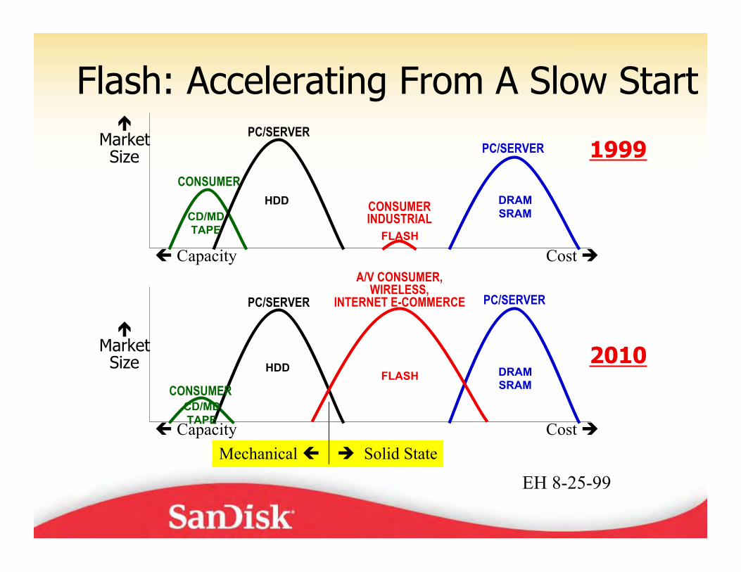
Flash: Accelerating From A Slow Start
MarketSize 1999
CONSUMER
PC/SERVER
CONSUMERINDUSTRIAL
PC/SERVER
CD/MDTAPE
HDD
FLASH
DRAMSRAM
Capacity Cost
MarketSize 2010
CONSUMER
PC/SERVER
A/V CONSUMER,WIRELESS,
INTERNET E-COMMERCE PC/SERVER
CD/MDTAPE
HDDFLASH DRAM
SRAM
Capacity Cost Mechanical Solid State
EH 8-25-99

Projected NAND Demand:~20X from 20062010
Source: Gartner Dataquest, November 2006
Imaging Video & PCAudioData
Billions ofMB
Lifestyle Storage
-
2,000
4,000
6,000
8,000
10,000
12,000
14,000
16,000
2000 2001 2002 2003 2004 2005 2006 2007 2008 2009 2010
Other A utomotive PC Gaming Mobile Phone Camcorder USB Drive Media Player Digital Camera
15.4 Trillion MB
1.4 Billion MB
Media Player
Mobile Phone
PC
USB

Mobile/CE/PC Driving NAND Future
Music Phone
Camera PhonePDA Phone
Game Phone
Video Phone
GPS Phone
MobileTV
PC, C
E M
arke
ts
M
obile
Mar
ket
Email Imaging Music GameVideo Map TV / STB
Application

Pioneered by SanDiskStandardized by thePCMCIA Association
Introduced by SanDiskin 1994
Introduced bySanDisk and Siemensin 1997
Introduced by SanDisk,Toshiba and Panasonicin 1999
Introduced bySanDisk and Sony in2000
Introduced by SanDiskin March 2003Standardized in
Jan 2004
Introduced by SanDisk inMarch of 2004Standardized in
May 2005
Industry Standards—Key to Mega-Markets
Introduced bySanDisk and M-Systems in 2005
Introduced bySanDisk in
Sep 2005
MicrosoftMay 2007

Flash: A License to Disrupt
• Past 10 years:– 35mm film– Floppy, Zip, Clik– Tape– CD– 1.3” KittyHawk, 1” Microdrive,
.85” Drive– NOR Flash
• Next 5-7 years:– 1.8” HDD– DRAM ?– DVD ?– 2.5” HDD ?
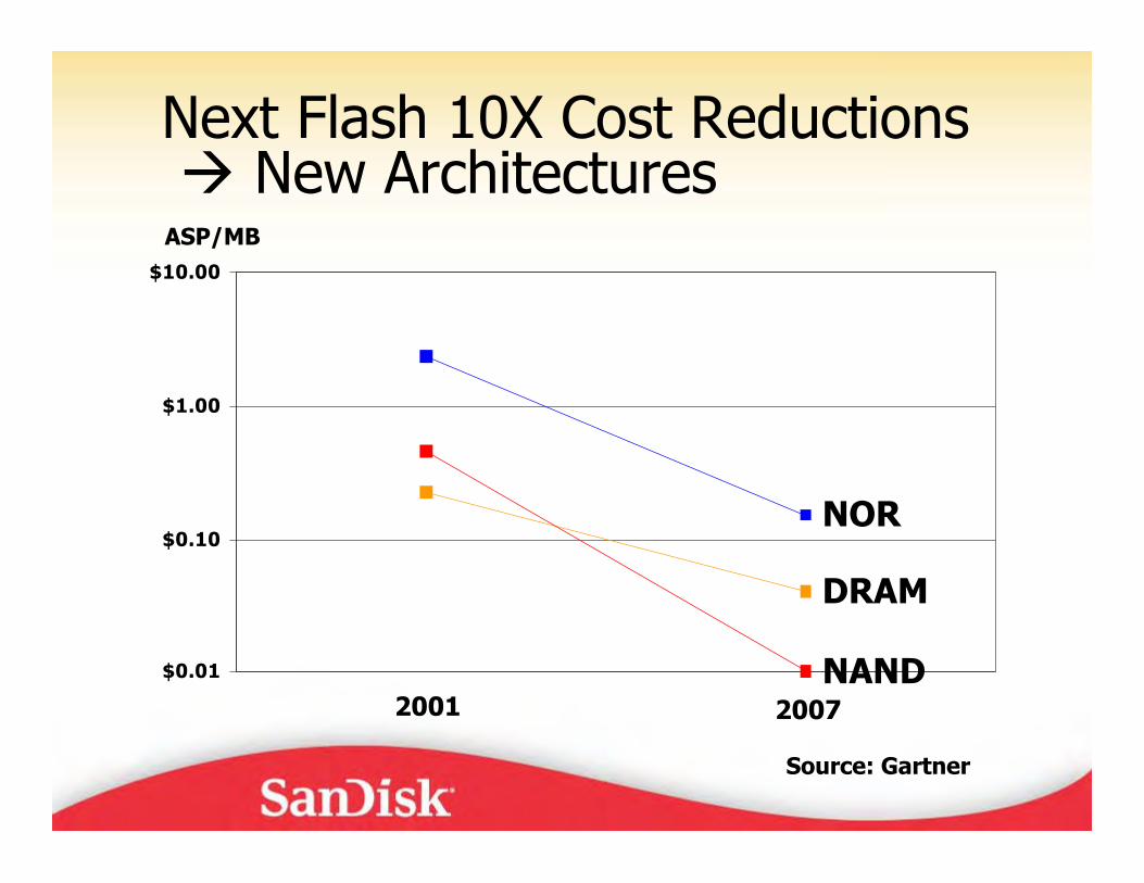
Next Flash 10X Cost Reductions New Architectures
$0.01
$0.10
$1.00
$10.00
DRAM
NAND
ASP/MB
NOR
Source: Gartner
2001 2007

Market Pull
• Digital revolution creating new mega-markets
• Price-elastic demand from consumer markets
• 1 Billion new consumers

NAND Technology &Challenges

NAND: A Remarkable Technology
• NAND Flash has become process technologydriver for the semiconductor industry
• NAND’s unprecedented scaling rateoutstripping lithography, other toolscapabilities

New TOX Process
New STI gap fill material
New gate material
New inter polydielectric material
New tunneloxide process
Increasing Process Complexity

Technology Push
• NAND rapid scaling benefits from:– Simple array architecture, 4F2, self aligned– Si Floating gate >30 years industry experience– Carry-over between successive generations– Tunnel write/erase current massive parallelism– Multi-level cell (x2 now, x3, x4 in next few years)
• However, NAND as we now know it mayapproach practical limits in ~ 4 generations(~20nm) at ~256Gbit
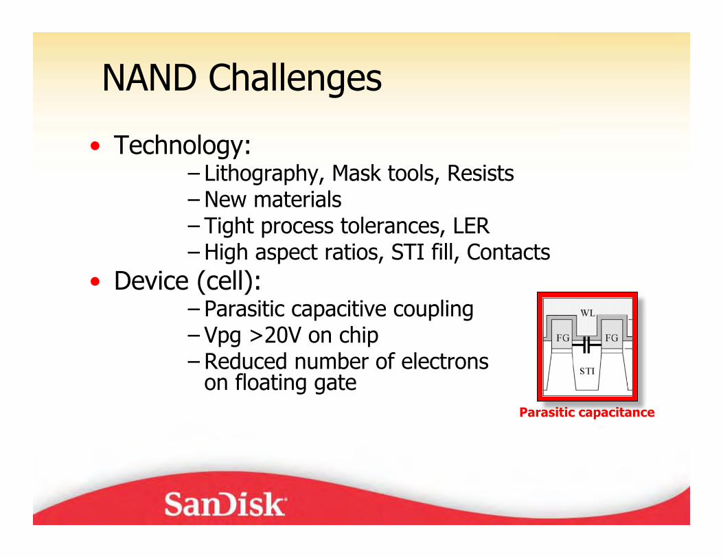
NAND Challenges
• Technology:– Lithography, Mask tools, Resists– New materials– Tight process tolerances, LER– High aspect ratios, STI fill, Contacts
• Device (cell):– Parasitic capacitive coupling– Vpg >20V on chip– Reduced number of electrons
on floating gateParasitic capacitance

Logical Scaling: Beyond 2b/c4 bits/cell16 levels
1111
0000
0010
1 bit/cell2 levels
0 1
2 bits/cell4 levels
00 01 10 11
0011
0100
0101
0110
0111
1000
1001
1010
1011
1100
1110
1101
0001
3 bits/cell8 levels
000
001
010
011
100
101
110
111
Syst
em E
xper
tise
Incr
easi
ngly
Im
port
ant

System Solution Becoming Critical
• Flash Memory Chip+ Controller– Defect management, wear-out leveling, cell-cell
interference mitigation
– Mass storage emulation, file/bad blockmanagement
– Standard I/O (hide chip algorithmic changes)
– Performance boosting
– DSP, Powerful ECC to enable x4

NAND Manufacturing

Dynamics Of NAND Fabs
• In past 2 years, 200mm DRAM NAND capacityconversion to capture higher margins
• >50% of current industry-wide NAND capacity is200mm, becoming obsolete in ~12 months
• Projected annual ASP/MB cost reductions of~40% in next 5 years (best performers)
• ~60% annual ASP/MB price reductions of2006/7 not sustainable going forward

NAND Economies of Scale: $5B+ per FabAS of Jan 26 2007
AS of May 8 2007
Y3 Y4

Short Technology Life Cycles
0%
10%
20%
30%
40%
50%
60%
70%
80%
90%
100%
2004 2005 2006 2007 2008
43nm
56nm
70nm
90nm
130nm
Source: SanDisk
% of production
5 generations in 5 years in production
Flash Competitors

Flash Competitors & Alliances

Competing NVM Technologies

Contenders
• CTF: NAND SONOS/TANOS• NROM/Mirror Bit/Quadbit• PCM/Ovonic• Magnetic RAM (MRAM), Ferroelectric RAM• Probe/Milipede• 3D: Diode , NAND

Required Breakthrough: Write/Erase Switching
3D Memory-Disrupting NAND, HDD?

Conclusions

Summary: NAND at Center Stage
• Young, fast-growing mega-markets for Flashstorage
• Flash a disruptive/enabling force in CE, PC• Huge manufacturing scale and IP required to
compete• Flash device scaling challenges will dictate system
level solutions
• Flash’s 10X cumulative cost reductions innext 5-7 years will complete Flash’s journeyto Center Stage

The Future of Flash Memory is …NOW, and EVERYWHERE!