nanotechnologyacademic.pgcc.edu/~sjohnson/nanolecture_egr101.pdfnanotechnology natural engineering...
TRANSCRIPT

NanotechnologyNatural Engineering
● The nanometer range is the size of molecules● Nanotechnology is simply molecular engineering● Life itself can be viewed as being natural molecular
engineers– Oxygen generation– The programming code of life
● Humankind has been using nanotechnology for centuries (of course without complete understanding)

NanotechnologyOld and New
● Nanotechnology is in part old technology– Nanoparticles have been utilized for many centuries albeit
with out the understanding● The creation of bread is at the nano-level● The creation of certain stained glass windows utilizes
nanoparticles– Gold (and silver) at the nanoparticle level is observed as different
colors such as red, orange, green, yellow– Can manipulate grain size to produce different effects
– Modern nanotechnology starts with the buckyball
● Nanotechnology is now being understood– Allows for advances through theory and simulation– Modeling is very important in this research

Buckyball The start of the modern nanotechnology history

NanotechnologyThe buckyball
● C60 is referred to as a buckyball and has a distinct shape like a old-style soccer ball
● Buckyball (part of the fullerene family)– Truncated Icosahedron– 0.7 nm in diameter with a spacing of 1 nm between
adjacent buckyballs– Inert– Can be made in to superconductor– Offshoot studies led to the discovery of the nanotube– The most massive particle to show wave-particle duality
(Nature 1999)

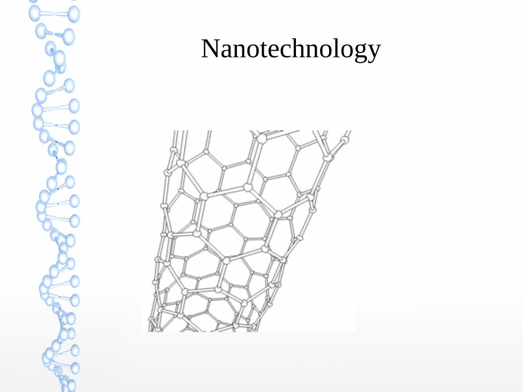
NanotechnologyThe Nanotube
● Nanotube (part of the fullerene family)– Few nm in diameter– Length can be as long as it can be made

NanotechnologyHistory
● C60 was produced in 1985 during an experiment to determine what signature carbon molecules might be generated in space
– Stars have carbon surrounding them– The C60 was a unintended by-product
● Nanotube– First observed in 1991, produced in 1992– Interest in buckyball technology shifted to nanotubes (for
the most part)
Nanotechnology

Nanotechnology

Nanotechnology
● Different “wraps” of the nanotubes produce different results
– m=n are metallic (armchair above)– Others are semiconductors, though there are
exceptions– Check out Dr. Sinex's Excelets on this

Nanotechnology
● Technology at the nanoscale (10-9 meters)– Bioengineering
● Bionanosensors● Biochips
– Environmental Engineering● Nanomembranes● Nanocatalysts
– Material Engineering (Mechanical/Civil/Chemical/Aerospace/etc.)
● Quantum dot● Nanocoating

Nanotechnology● Technology at the nanoscale (10-9 meters)
– Electrical Engineering (Electronics)● Lithography (already at nanolevel)● DNA chips● Nanowires● Bionanosensors (yes, this is in Bioengineering)● Biochips (yes, this is in Bioengineering)● Nano-optics
● Nanotechnology ranges from 1 nm to 100 nm– Only one dimension in this range is required to be called
nanotechnology– Many electronic chips already have components in this range– Coatings at this range are commonplace

NanotechnologyThree “types” of Nanotechnology
● Wet nanotechnology– Water environment– Biological– Cellular level, membranes
● Dry nanotechnology– Carbon, silicon, other inorganic materials– Metals, semiconductors– Too reactive; can't operate in wet conditions
● Computational nanotechnology– Modeling and simulation of complete nanostructures– Required to understand nanotechnology

Nanotechnology
● Surface effects, chemical effects, physical effects are different in the nanoscale then in the macro or micro scale
– This creates new and interesting products● Stain resistant clothes● Sweat absorbing clothes
– This also creates new avenues of research● New exciting discoveries wait● Some disappointments await as well● Nature of research

Nanotechnology
● Top-down– Build nanotechnology using larger elements– No atomic-level control– Nanolithography
● Bottom-up– Build from molecular components– Components assemble themselves using molecular recognition
● Self-assembly● Needs some for of coding
– What in nature might be used as a model for this?– What are some issues with the use of this?

Nanotechnology
● DNA is a coding device that is used in nature● DNA is nanometer in size● DNA faces: Paul Rothemund
Nanotechnology
● Nanotechnology spans all disciplines and is too extensive to be done complete here
– Use examples to try and show some interesting possibilities– Wet, dry, and computational
● Why the understanding of Physics is a must– Concepts that are important
● Scaling laws● Quantum mechanics
– Hartree-Fock– Transport phenomena
● Surfaces– Hydrophobic and hydrophilic– Diffusion, transport in all dimensions

NanotechnologyEnvironment
● Water Purification– Humans need clean consumable water for survival– Environmental contaminants are a serious problem
● Nanotechnology to the rescue?– Ceramic nanomembrane
● Ultrafiltration● Reactive component (iron oxide ceramic membranes) add an extra-level of
removal● Aluminum oxide ceramic membranes are another membrane being
investigated– Iron remediation
● Nanoscale powder– Iron oxidization causes certain organic molecules (including the toxic ones) to break down– Nanoscale iron is more reactive then larger iron grains– Small size allows it to move between soil particles

NanotechnologyMaterials
● Nanocrystalline metals– What are they?
● All metals are crystalline with the grain size an important characterization that defines among other things the yield strength
● Hall-Petch equation (below)– Implies small grain size gives better yield strength– Certainly valid for microcrystalline structures, but questions remain about
nanocrystalline structures– Cons: Corrosion, creep worse
● Observation of small grain size has suggested increase yield strength, but at levels not consistent with Hall-Petch
– Observed negative Hall-Petch effect– Questions remain; studies needed
– Future shows promiseσ y=σ0+
k
d12
σ y= yield strengthσ0 ; k=constant dependant onmaterial

NanotechnologyMaterials
● Bone– Large portion of bone is nanosize hydroxyapatite– Repair could be possible using bioactive and
resorbable ceramics– Mechanism would be osteoinduction

NanotechnologyMaterials
● Spintronics (or magnetoelectronics)– Use the spin of the electron rather then the movement of
the electrons– For technology the promise is to make faster, smaller
transistors– So why is this nanotechnology? An electron certainly is
not nanometer is it?– Technically spintronics is not nanotechnology, however
nanotechnology offers the best approach for its practical use
– Create ferromagnetic semiconductors that require layers that are only a few nanometers ( there you go)←

NanotechnologyMachines
● Nanoparts are uses for micromachines...an actual nanomachine is less practical
● Motion is controlled by some form of voltage● Nanomotor
– Using multi-walled nanotubes– One tube rotates inside the other– In effect have rotational bearings
● Molecular actuator– Nanomotor controlled by the use of a nanocrystal ram
● Nanoelectromechanical relaxation oscillator– Liquid metal droplets exchanging mass– Utilizes surface tension (which is very strong)
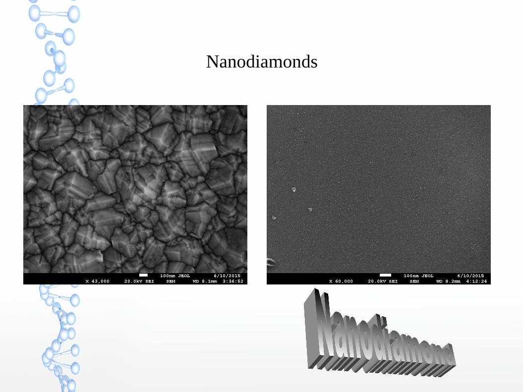
Nanodiamonds

NanotechnologyTools
● Electron microscopes– Scanning electron microscope (SEM)
● Focused beam of electrons● Electrons much smaller than1 nm● 5 to 10 nm resolution; 1 nm ● Surface scanner
– Transmission electron microscope (TEM)● Electrons penetrate sample● Magnets used to bend the electrons● 0.2 nm resolution
– Analytic electron microscope (AEM)● TEM with equipment like spectrometers● 0.1 nm resolution
● Scanning Probe Microscopes (SPM)– Uses probes– Scanning tunneling microscope (STM) and atomic force microscope (AFM)
● Nanomanipulators

NanotechnologyTools
● Theory, Modeling, and Simulation (TMS)● TMS is most important tool presently
– Main idea is to study nanotechnology to direct how to use it better– Need to interpret data– Need models of measuring tools and materials to understand interaction
● Follows the standard protocol– Theory: what do we know about the materials and tools– Model: represent our theory in a testable fashion (equations; numerical analysis
techniques)– Simulate the model to see if it gets us the test results
● Success – use the model to predict some new result– Test for new result to confirm model
● Failure (not computer failure (bugs), but failure of the model)– Re-work model– Investigate theory

Nanotechnology is Nano-everything
● Nanotechnology– Nanomaterials
● Semiconducting nanostructures– Buckyballs– Nanotubes– Nanowires– Nanoparticles
● Metallic nanostructures– Nanoelectronics– Nano-optics– Nanomechanics– Nanofluidics– etc.

26
PGCC courses that discuss nanotechnology
Materials Science course (EGR 2300) http://academic.pgcc.edu/~sjohnson/egr230.html
General Chemistry for Engineers (CHM 2000) http://academic.pgcc.edu/~ssinex/chm2000.htm
Introductory Engineering's “Introduction to Nanotechnology” module http://academic.pgcc.edu/~sjohnson/nanotech.html
Honors Seminar (EGR 2990) http://academic.pgcc.edu/~sjohnson/egr299.html

27
PGCC web sites for the excelets (used to support Materials and
Chemistry) Materials Science excelets
http://academic.pgcc.edu/~ssinex/excelets/matsci_excelets.htm
General Chemistry excelets http://academic.pgcc.edu/~ssinex/excelets/chem_excelets.htm

PGCC supports(which include some materials science and nanotechnology)
● PRDM Website - Howard, Cornell, Gallaudet, and PGCC
● CIQM Website - Harvard, Howard, MIT, Gallaudet, Boston Museum of Science and PGCC

Nanotechnology websites● http://cnst.rice.edu
● http://cnms.ornl.gov
● http://www.nano.gov
● http://www.nanotechinstitute.org
● http://www.nanotechweb.org
● http://www.nanohub.org
● http://www.nano.org.uk
● http://www.nanoscienceworks.org
● http://www.nanotechproject.org/consumerproducts
● http://www.nbtc.cornell.edu
● http://nanocenter.umd.edu
● http://www.sciencemuseum.org.uk/antenna/nano/
● http://nano.tm.agilent.com
● http://www.nanowerk.com● http://en.wikibooks.org/wiki/The_Opensource_Handbook_of_Nanoscience_and_Nanotechnology

Materials/Nanotechnology Simulators/Demos/Games
● Duckboy nanotechnology demonstration
● Molecular Workbench
● Microscope Simulators (Windows/Mac OS only)

Materials
Backup slides for interest only
● Scale is an important issue in nanotecnology● Just compare volume compared to surface area
– Strength proportional to cross sectional area– Weight proportional to volume– Strength/weight
● Elephant ~ 1● Flea ~ 1000

Mechanical scaling
● Mechanics scaling– Mass is proportional to volume (think density)
● Gravitational force is proportional to volume– Therefore frictional force is proportional to volume as well,
but at very small scale van der Waal forces dominate, therefore “striction” force is proportional to contact area
● Spring force is proportional to length● Kinetic energy is proportional to volume (mass)● Potential energy for gravity is proportional to volume● Potential energy for a spring is proportional to area● Etc. Hope you get the idea...

Molecular Dynamics (MD)
● Van der Waal forces– Covers close range and long range forces– Repulsive force and attractive force– Describe in MD simulation by Mie-Jones 6-12 or
Lennard-Jones
– Epsilon and sigma are material dependent – Epsilon is “well depth” – Sigma is “hard repulsion” radius
V LJ=[ vdw
rij 12
− vdw
rij 6
]

Van der Waals revisited
● Van der Waal forces– Note force is derivative of energy– Reason Gecko's stick to walls
● Nanohairs● Lots of surface area● Beats gravity
– Keeps us from going through walls● We touch things or do we?

Scales in Nanorealm
● Melting point is effected by dimensions
– Where D is in nanometers– Imagine 1 nm scale!
T m=T m ,bulk [ 1− 1D ]

Scales in Nano-realm
● An elements bulk crystal structures is not necessarily the same in the nanotechnology realm
– Ruthenium at 2 to 3 nm can have bcc and fcc (normally hexagonal)
– Van der Waal interactions dominate

Scales in Nano-realm
● Geometry of wires matter because of volume to surface area ratio
– High surface-to-volume ratios in nano-realm– Gallium nitride < 100 nm will emit different
wavelengths of light if having different dimensions (wire, belt, rod)

Scales in Nano-realm
● Porous Materials– Zeolites
● Many tunnels; network of “caves”● Cavities 200 to 2000 pm● Pores 300 to 1000 pm● Guest molecules (water)● 56 zeolites
– Aluminosilicates most common– Metal-organic framework
● Clay that are like zeolites● Up to 4500 sq. meters/g

Scales in Nano-realm
● Porous Materials– Zeolites
● Captures clogging charged Magnesium, Calcium in pores; softens water
● Sieves (filter)● Create catalysts (lots of surface area)● Filter & Catalyst better than conventional material● Shape-selective catalysis
– Reactant: only molecules of a given dimension enter and reach the catalyst
– Product: only molecules of a given dimension get get out– Transition state: certain reactions stopped because product
is too big for cavity

Scales in Nano-realm
● Small-grain material– Grain size determines deformation
● Plastic deformation equation– Hall-Petch equation– Where k is constant, d is grain size in micrometers– Accurate for grain size 100 nm to 10 micrometers– Below 30 nm not accurate– At very small size the grain boundaries act more like a web
● Diffuse, migrate, and slide instead given different effects
● Probably below 30 nm the material gets brittle, but hard to tell because melting point drops as well....arg!
y=ok
d whereo is frictional stress
N
m2which oppose dislocation