n e a r e a s tdocs.neu.edu.tr/library/1584431819.pdf · n e a r e a s t u n i v e r s i t y ......
TRANSCRIPT
N E A R E A S T
U N I V E R S I T Y
COMPUTER ENGINEERING DEPARTMENT
S P E C I A L P R O J E C T R E P O R T
C O M 4 0 0
INTERFACING TECHNIQUES
OF RAM DEVICES TO THE
MICROPROCESSOR
J U N E 1 9 9 5
ADVISOR: BY:
HALIL ADAHAN. AYNUR TURKKAL.
RAMIS YAVAS.

AYNUR TURKKAL C
COMPUTER ENGINEERING DEPT.
90220.
RAMIS YAVAS.
COMPUTER ENGINEERING DEPT.
91530.
C O N T E N T S
T I T L E P A G E N 0
CONTENTS----------------------------------------
ACKNOWLEDGEMENTS---------------------------------
PREFACE------------------------------------------
INTRODUCTION-------------------------------------
CHAPTER 1---------------------------------------- 01
The Microprocessors,in general------------------- 01
CHAPTER 11--------------------------------------- 03
The Motorola 6800 Microprocessor----------------- 03
The 6800 pin diagram----------------------------- 04
Pin definitions---------------------------------- 05
The 6800 architecture---------------------------- 08
Registers---------------------------------------- 09
The Stack Pointer-------------------------------- 10
Arithmetic and Logic Unit------------------------ 11
Instruction Decoder------------------------------ 11
The Interrupt and Control Unit------------------- 11
CHAPTER 111-------------------------------------- 11
Microprocessor Interfacing----------------------- 11
Block diagram of Microprocessor Based Design----- 12
Interfacing with ROM----------------------------- 13
Interfacing with RAM----------------------------- 18
CONCLUSION--------------------------------------- 25
APPENDIX A--------------------------------------
APPENDIX B---------------------------------------

A C K N O W L E D G E M E N T S
We would like to thanks Mr. Halil ADAHAN for his valuable help in preparation of our report.

P R E F A C E
This report has been written from students who are in COMPUTER ENGINEERING DEPARTMENT at NEAR EAST UNIVERSITY for graduation project.
The purpose of this work is to provide to explain the microprocessor interfacing.
INTRODUCTION
Most microprocessors in a stand alone fashion do not contain substantial memory. To increase the power of a microprocessor we have to interface I/0 modules. The interconnection, or linkage, of the parts within this system is called interfa cing. Generally, an interface is a shared between two or more devices which utilize information. Other considerations in interfacing include synchronization, direction of data trans mission, and sometimes the adjustment of signal levels or mo dels.
Interfacing deals with the synchronization and transmission of data to and from the MPU, and therefore the software as well as the hardware must be considered in great detail.
Generally, data transfers in and out of the MPU over the bus ses take the form of one of these activities:
1- Memory read 2- Memory write 3- I/0 read 4- I/0 write 5- Interrupt or reset handling.
When it is said that is input from another device, it means input in relation to the MPU. Likewise, an output would be output from the microprocessor unit. Generally, the micropro cessor is the focus of all operations, but in some cases the MPU relases control of the address and data bus so that the peripheral device may access the main system memory directly going to the MPU. This is called DMA (Direct Memory Access).
The processor itself uses MPU, ROM, and RAM externally, and its of importance that the manifactures produce peripheral interface adapters that are compatable with other micropro cessors units. These are generally general purpose in that they can be programmed to function as either input or output interface programmable communication devices. Manufactures p roduce specialised interface component IC (Integrated circu it)'s which are programmable DMA controllers, programmable interrupt controllers, diskette controllers, synchronous data link controllers, and keyboard/display controllers.
General purpose of interfacing, microprocessor can READ/WRITE using memory (ROM or RAM) capacities or more memory capaci ties.
CHAPTER 1
THE MICROPROCESSORS IN GENERAL
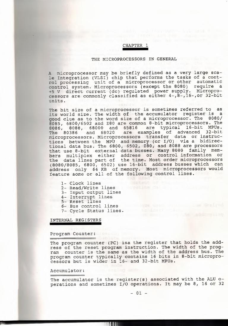
A microprocessor may be briefly defined as a very large sca le Integration (VLSI) chip that performs the tasks of a cont rol processing unit of a microprocessor or other automatic control system. Microprocessors (except the 8080) require a +5 V direct current (de) regulated power supply. Micropro cessors are commonly classified as either 4-,8-,16-,or 32-bit units.
The bit size of a microprocessor is sometimes referred to as its world size. The width of the accumulator register is a good clue as to the word size of a microprocessor. The 8080/ 8085, 6800/6502 and Z80 are common 8-bit microprocessors. The 8086, 8088, 68000 and 65816 are typical 16-bit MPUs. The 80386 and 68020 are examples of advanced 32-bit microprocessors. Microprocessors transfer data or instruc tions between the MPU and memory (or I/0) via a bidirec tional data bus. The 6800, 6502, Z80, and 8088 are processors that use 8-bit external data busses. Many 8080 family mem bers multiplex either address or control information or the data lines part of the time. Most order microprocessors (8080/8085, 6800, 6502) use 16-bit address busses which can address only 64 KB of memory. Most microprocessors would feature some or all of the following control lines.
1- Clock lines 2- Read/Write lines 3- Input output lines 4- Interrupt lines 5- Reset lines 6- Bus control lines 7- Cycle Status lines.
INTERNAL REGISTERS
Program Counter:
The program counter (PC) isa the register that holds the add ress of the reset program instruction. The width of the prog ram counter is the same as the width of the address bus. The program counter typically contains 16 bits in 8-bit micropro cessors but is wider in 16- and 32-bit MPUs.
Accumulator:
The accumulator is the register(s) associated with the ALU o perations and sometimes I/0 operations. It may be 8, 16 or 32
- 01 -

bits wide. The 8080/8085, 6800, and 6502 MPU's all have 8-bit accumulators. Some processors (68000 and Z80) have only ge neral purpose registers that may be used as accumulators.
Status Register or Flags:
The status register is available on all microprocessors. The individual bits in the register are called flags. The condi tions of the flags are generally associated with ALU opera tions and are used by subsequent branch and jump instructions for decision making.
General Purpose Registers:
General purpose registers may be used to temporarily store data or hold an address. They are not assigned a specific task. In 8-bit microprocessors, general purpose registers can not function as an accumulator in ALU and I/0 operations. How ever, 16-bit MPUs usually allow general purpose register to be used as accumulators.
Index Register:
The index register is used to hold the address of an operand when the indexed address mode is used (8080/8085, 6800, 6502, Z80, 8086). General-purpose registers are used as index re gisters on the Z80 and 68000 microprocessors.
Stack pointer Register:
The Stack pointer (SP) is a specialized register that keeps track of the next available memory location in the stack. The stack is reserved area in RAM used for temporary storage of data, return addresses, and content of registers. The stack is used during subroutine calls and interrupts.
ADDRESSING MODES:
An addressing mode is the technique used to fetch the desired operand during the execution of an instruction. Induvidual microprocessors may not use all of the addressing modes listed below:
1 - Inherent (implied) addressing mode 2 - Immediate addressing mode 3 - Extended or absolute addressing mode 4 - Register addressing mode 5 - Register indirect addressing mode 6 - Index addressing mode 7 - Zero page (direct) addressing mode 8 - Relative addressing mode 9 - Based addressing mode 10- Based index addressing mode 11- String addressing mode 12- I/0 addressing mode 13- Status register addressing mode.
- 02 -
Generally, the more modern 16-bit computers have powerful and flexible addressing modes.
CHAPTER II
THE MOTOROLA 6800 MICROPROCESSOR
The motorola MC6800 is an 8-bit microprocessor functionally, the data bus is 8-bit and the address bus is 16-bits. An MPU chip such as the- 68HC11,includes an 8-bit microproces sor a timer, ROM, RAM, and A/D converter, and an on-chip os cillator the functionalities providing also programmable I/0 lines and an EPROM.
The MC68000 is an advanced 16-bit microprocessor other mem bers of the motorola family are the 68HCOOO (CMOS), 68008, 68010, 68020, and 68030. The 68000 MPU features and 32 bit internal architecture with a 16 bit external data bus and it can address 16 MB of memory. The 68010 is an updated 16 bit external/32 bit internal virtual memory.
The 68020 supports a 32 bit internal/external virtual memory is a advanced feature of MPU's. Virtual memory means that a programmer can write programs as it memory capacity is unlimited. Type of PC programs that use virtual memory.
1- WINDOWS 2- ACAD 3- MICROSOFT EXEL 4- 3D STDIO 5- COREL DRAW 6- MATHEMEDICA 7- MAT LAB.
The virtual memory technique permits program to be larger than the capacity of the main memory. The extra part of the program is stored on a secondary storage medium (DISK).
- 03 -
CLOCK ¢1, ¢2
¢1: Supplies the required clock cycles to increment the in ternal register.
¢2: Provides the necessary clock cycles to fetch and execute an instruction.
I • I I I I I I Yi N vi :~ ¢1 l I I I I I :
l I I I • • I l I I I I I I ¢2 I I
~ l
V ~ I I V l I I
I I I I I I I I I I I
ROM (READ ONLY MEMORY)
ROM is a read only memory containing monitor subroutines+ display routines+ timer control subroutines. It is medium-scale integration (MSI).
RAM (RANDOM ACCESS MEMORY)
Where the programs are executed.
PIA (PERIPHERAL INTERFACE ADAPTER)
PIA has two I/0 parts. Each port is 8-bit ports A & B can be programmed to interface I/0 devices.
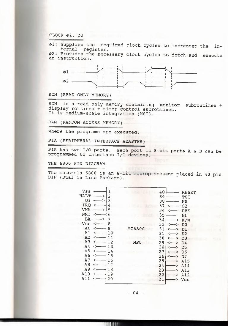
THE 6800 PIN DIAGRAM
The motorola 6800 is an 8-bit microprocessor placed in 40 pin DIP (Dual in Line Package).
Vss 1 40 RESET HALT--> 2 39 TSC
Ql --> 3 38 NS IRQ < 4 37 <- Q2 VMA --> 5 36 <-- DBE NMI < 6 35 NL BA--> 7 34 > R/W
Vee < 8 33 <-> DO AO< 9 MC6800 32 <-> Dl Al < 10 31 <-> D2 A2 < 11 30 <-> D3 A3 < 12 MPU 29 <-> D4 A4 < 13 28 <-> DS AS< 14 27 <-> D6 A6 < 15 26 <-> D7 A7 < 16 25 > Al5 AS< 17 24 > A14 A9 < 18 23 > Al3
AlO < 19 22 > Al2 All < 20 21 > Vss
- 04 -
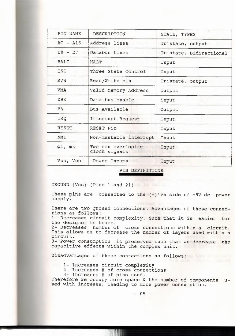
PIN NAME DESCRIPTION STATE, TYPES
AO - Al5 Address lines Tristate, output
DO - D7 Databus Lines Tristate, Bidirectional
HALT HALT Input
TSC Three State Control Input
R/W Read/Write pin Tristate, output
VMA Valid Memory Address output
DBE Data bus enable input
BA Bus Available Output
IRQ Interrupt Request Input
RESET RESET Pin Input
NMI Non-maskable interrupt Input
¢1, ¢2 Two non overloping Input clock signals
Vss, Vee Power Inputs Input
PIN DEFINITIONS
GROUND (Vss) (Pins 1 and 21)
These pins are connected to the (-)'ve side of +5V de power supply.
There are two ground connections. Advantages of these connec tions as follows: 1- Decreases circuit complexity. Such that it is easier for the designer to trace. 2- Decreases number of cross connections within a circuit. This allows us to decrease the number of layers used within a circuit. 3- Power consumption is preserved such that we decrease the capacitive effects within the complex unit.
Disadvantages of these connections as follows:
1- Increases circuit complexity 2- Increases# of cross connections 3- Increases# of pins used.
Therefore we occupy more space & the number of components u sed with increase, leading to more power consumption.
- 05 -
HALT (Pin 2)
When the halt input is activated by a LOW, the 6800 MPU en ters the halt mode. In this mode the tri-state lines go to their high impedence state and the processor stops executing instructions. This input could be used for "single stepping'' in a program in the debugging process. The halt input is disabled by connecting it to +5 V de.
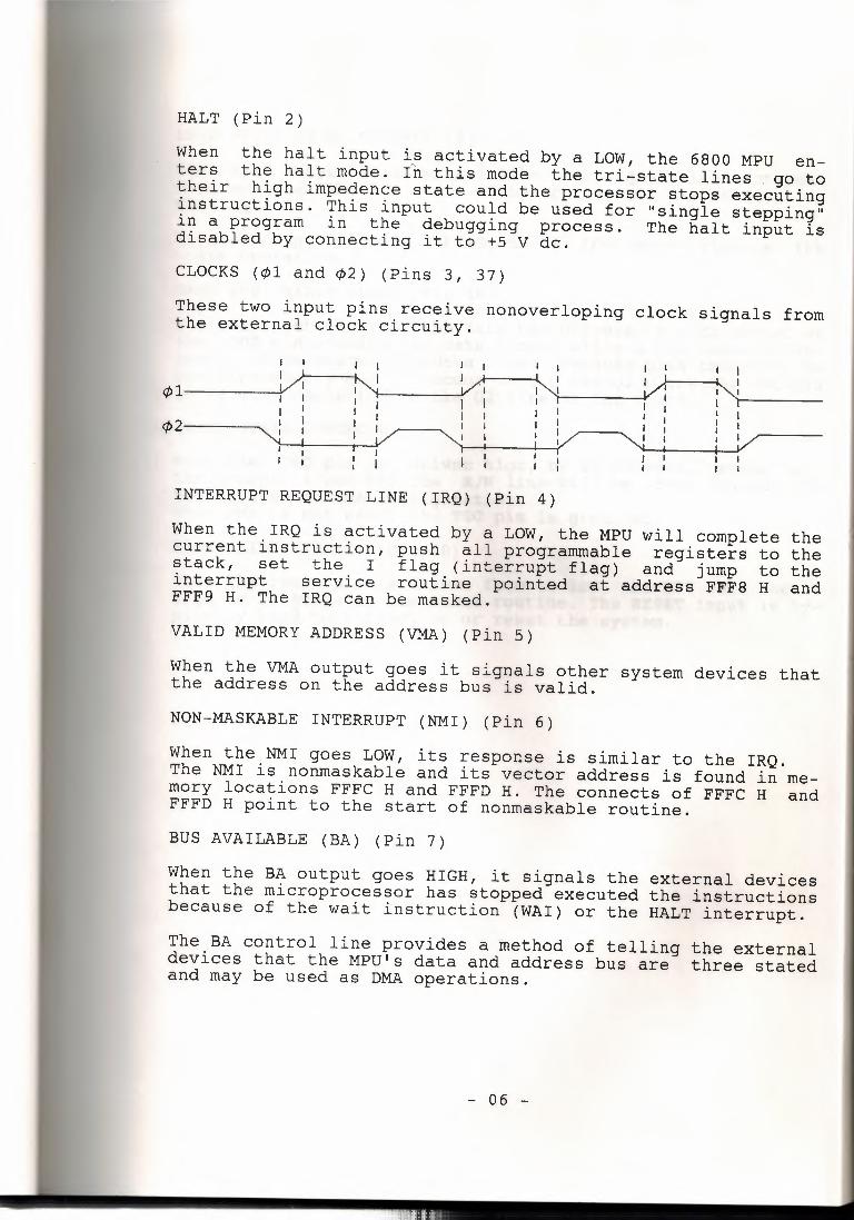
CLOCKS (¢1 and ¢2) (Pins 3, 37)
These two input pins receive nonoverloping clock signals from the external clock circuity.
I I I I I I I I I I I I I I N ~: N ~ N ¢1 ,/i I I I I I I I I l I I I I I I I I I I I I I I I ¢2 I I I i I I I I "1 I I v ~
I I :/ ""1 I I V I I I I I I I I I I I i I I I I I I I I I I I I I I I I I I
INTERRUPT REQUEST LINE (IRQ) (Pin 4)
When the IRQ is activated by a LOW, the MPU will complete the current instruction, push all programmable registers to the stack, set the I flag (interrupt flag) and jump to the interrupt service routine pointed at address FFF8 H and FFF9 H. The IRQ can be masked.
VALID MEMORY ADDRESS (VMA) (Pin 5)
When the VMA output goes it signals other system devices that the address on the address bus is valid.
NON-MASKABLE INTERRUPT (NMI) (Pin 6)
When the NMI goes LOW, its response is similar to the IRQ. The NMI is nonmaskable and its vector address is found in me mory locations FFFC Hand FFFD H. The connects of FFFC H and FFFD H point to the start of nonmaskable routine.
BUS AVAILABLE (BA) (Pin 7)
When the BA output goes HIGH, it signals the external devices that the microprocessor has stopped executed the instructions because of the wait instruction (WAI) or the HALT interrupt.
The BA control line provides a method of telling the external devices that the MPU's data and address bus are three stated and may be used as DMA operations.
- 06 -

READ WRITE (R/W) CONTROL (Pin 34)
The R/W output is a control lihe that signals the external devices (i.e RAM, ROM etc.) whenever the MPU is reading or writing.
A high output signals a READ, and a LOW output signals the write operation.
DATA BUS ENABLE (DBE) (Pin 36)
The DBE input controls the data bus drivers. A high output on the DBE pin enables the data lines, while a low input disab les or three states the data lines. Because data transfer to and from memory and I/0 occur during the Q2 clock,the DBE pin is usually connected to the Q2 line of the clock.
THREE STATE CONTROLS
When the TSC pin is driven high, by an external device all the address lines and the R/W line will be three stated. The TSC is used in DMA configurations. When DMA is not used, the TSC pin is grounded.
RESET LINE (RESET) (Pin 40)
When the reset pin is driven from to low, the MPU sets the I flag to 1, jumps to the reset routine. The RESET input is ty pically used to initialize or reset the system.
- 07 -
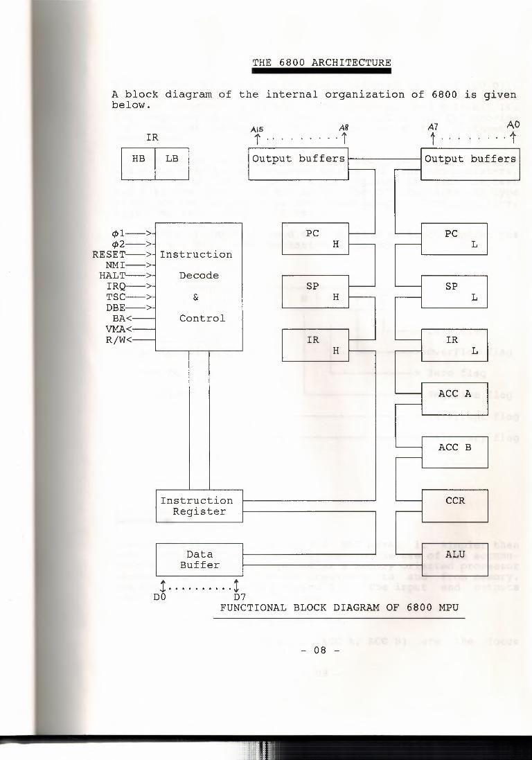
THE 6800 ARCHITECTURE
A block diagram of the internal organization of 6800 is given below.
¢1- ¢2-
RESET- NMI--
HALT- IRQ- TSC- DBE-- BA<
VMA< R/W<
IR AIS i .. AB ..... i A7 AO t .... ' .. ·t
TI Output buffers Output buffers .---
> PC ,___ PC > H ,___ L > Instruction > > Decode > SP .--- SP > & H i--- L > - Control - - IR IR
H .-- L
- ACC A .---
- ACC B .---
Instruction - CCR Register .---
Data ALU Buffer
1 x DO D7
FUNCTIONAL BLOCK DIAGRAM OF 6800 MPU
- 08 -
The MPU has an 8-bit three state buffered data bus (DO-D7). There are 16-bit buffered address bus. The MPU has 16-bit program counter, a 16-bit stack pointer, and a 16-bit IR. The temporary storage registers ACC A, ACC B, and CCR provide the register (temporary) allocation units for arithmetic operations.
The ALU performs the arithmetic and logic operations, in which the results are returned to any of the two registers, ACC A, ACC B, the CCR is an 8-bit register in which the test two bits are internally set of 1. The CCR indicates the type of the number in either of the accumulators (Type: positive, negative, zero, cary, half cary).
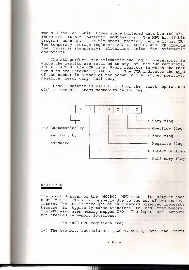
Stack pointer is used to control the stack operations with in the MPU. Stack mechanism as follows.
1 I 1 H I N z
Cary flag ~ [__> Auotomatically
set to 1 by
Owerflow flag
'--~~~~~~> Zero flag
hardware '--~~~~~~~-> Negative flag
'--~~~~~~~~~~> Interrupt flag
'--~~~~~~~~~~~~> Half cary flag
REGISTERS
The block diagram of the MC6800 MPU makes it simpler than 8085 unit. This is primerly due to the use of two accumu lators. The MPU is throught of as a memory oriented processor because it typically makes transfers to and from memory. The MPU also uses memory mapped I/0. The input and outputs are treated as memory locations.
The 6800 MPU registers are;
1-) The two bits accumulators (ACC A, ACC B) are the focus
- 09 -
<
of a large shane of the microprocessor operations. Accumu lator operation include arithmetic, logic, load, store, input and output. The second accumulator ACC B is just a general purpose register but a real accumulator in that all opera tions that can be performed in ACC B.
2-) The program counter(PC) is a 16-bit register that holds the address of the next instruction to be executed.
3-) The stack pointer(SP) is a 16-bit general purpose regis ter. The SP from a 16-bit address defines the top of the stack in the RAM.
4-) The index register(IR) is a general purpose register. Its primary use is to point and modify address.
5-) The condition code register (CCR) is an 8 bit register that contains the 6 flags which indicates the type of either the data or magnitude acted upon by ALU.
THE STACK POINTER
The SP is a 16 bit general purpose register that holds the p resent value of the stack address. The stack address is user defined by a set of allocatable memory locations. The SP is generally used for 2 purposes first is that it keeps reports of pointer address defined in the memory for I/0 operations. Secondary it's used in subroutine call instructions. When a subroutine is activated by the MPU, the process present add ress is diverted from its normal sequence of execution. Thus, the SP keeps record of return address, such that when subrou tine address is returned to the PC, allocates the main prog ram address. In such an execution process, the SP keeps re cord of the address in the stack of the programmable regis ters.
1 0 0 0 1 0 0 0
1 0 0 0 1 0 0 0
FLAGS
The MC 6800 uses six condition code flags. Thus is illustra ted below
STACK-> 1 0 0 0 0 0 0 0 0
These flags are used in branch instructions. Hence, each con ditional and unconditional branch instruction is decided ba sed on these six flags operated by the ALU.
Condition code register only reflects the condition of either ACC A or ACC B.
- 10 -

THE ARITHMETIC & LOGIC UNIT
The ALU is the heart of the microprocessor. It performs all arithmetic and logical operations. The result of the operati ons performed is stored either of the accumulators. The ALU performs such operations as adding, subtructing, comparing AND'ing, OR'ing, and XOR'ing.
INSTRUCTION DECODER
The instruction decoder interprets results from the instruc tion register. Based on these inputs, the instruction decoder directs the control section for execute the instruction.
THE INTERRUPT and CONTROL UNIT
The MPU will accept the interrupt signal from the interrupt input (INTR). Interrupts are generally classified to two ty pes. First one is the software driven interrupt, which is ac tivated by the MPU, and the hardware interrupt is activated using a hardware input using external devices.
CHAPTER III
MICROPROCESSOR INTERFACING
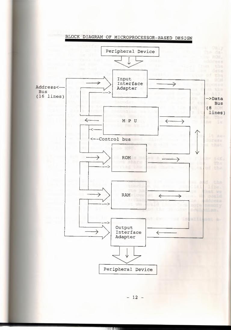
Our topic is microprocessor interfacing. Interfacing means that relation between the MPU and the memories. Introduction division is including the microprocessor interfacing.
General purpose of interfacing, microprocessor can write/read to/from memory (RAM/ROM) capacities or more memory capacities.
The block diagram of microprocessor based design. Suggests that the MPU, ROM, RAM, input interface adapter, and output interface adapter are separate devices. This may or may not be true depending on the specific system. It is quite common for manufacturers to produce peripheral interface adapters that are compatible with their microprocessor units. These are usually general-purpose in that thay can typically be p rogrammed to function as either an input or an output inter face device.
Some manufacturers integrate RAM and I/0 ports or ROM and I/0 ports on the same IC to decrease system component numbers. Manufacturers also produce specialized interface components in IC form. Some of these specialized components include p rogrammable communications interfaces, programmable DMA cont rollers, programmable interrupt controllers, diskette cont rollers, synchronous data link controllers, CRT controllers, and keyboard/display controllers.
- 11 -
Address< Bus
(16 lines)
BLOCK DIAGRAM OF MICROPROCESSOR-BASED DESIGN
Peripheral Device
Input ~-~~ ~I Interface
Adapter >
~ M P U
<--
<--Control bus
ROM 7 >
--) )I RAM
>
> Output Interface Adapter
7
Peripheral Device
j )
< )
I )
~ ~
/
"
->Data Bus
(8 lines)
- 12 -

#1 0000 H
I ~ 0 0 0 0 0 0 0 0 0 0 0 0 0 0 0
3FFF H 0 1 1 1 1 1 1 1 1 1 1 1 1 1 1
#2 4000 H I ~
1 0 0 0 0 0 0 0 0 0 0 0 0 0 0 7FFF H 1 1 1 1 1 1 1 1 1 1 1 1 1 1 1
#3 8000 H
I 1 0 0 0 0 0 0 0 0 0 0 0 0 0 0 0
BFFF H 1 0 1 1 1 1 1 1 1 1 1 1 1 1 1 1
#4 COOO H
I 1 1 0 0 0 0 0 0 0 0 0 0 0 0 0 0
FFFF H 1 1 1 1 1 1 1 1 1 1 1 1 1 1 1 1
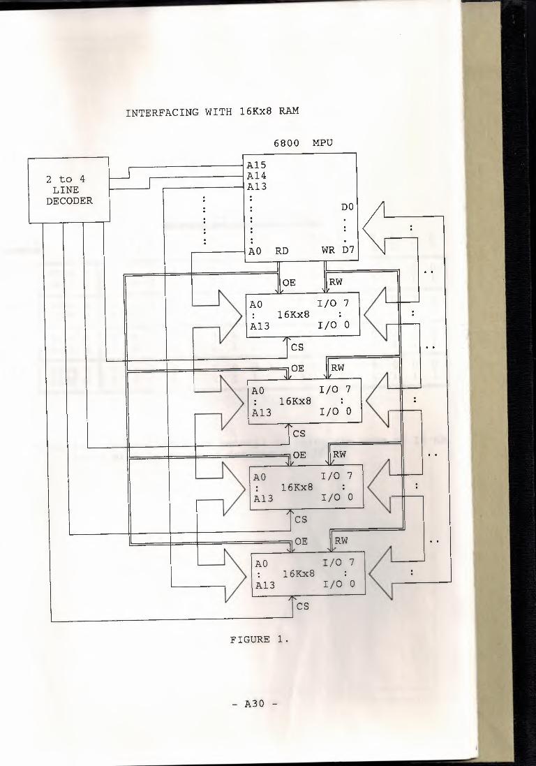
INTERFACING WITH 16Kx8 ROM 6800 MPU
2 to 4 LINE Al5
DECODER A14 A13 DO . . . . . . . AO RD D7
i
OE ' ,
AO 07 . 16Kx8 . . . Al3 00
Tes :> AO 11,0E 07 : 16Kx8 : A13 00
fcs .11.°E
AO 07 : 16Kx8 : Al3 07
Tes :> AO j"OE 07 : 16Kx8 : A13 07
Tes ADDRESS MAP FOR FIGURE 1
DEVICE A A A A 15 14 13 12
A A A A 7 6 5 4
A A A A 11 10 9 8
- 14 -
FIGURE 1.
A A A A 3 2 1 0
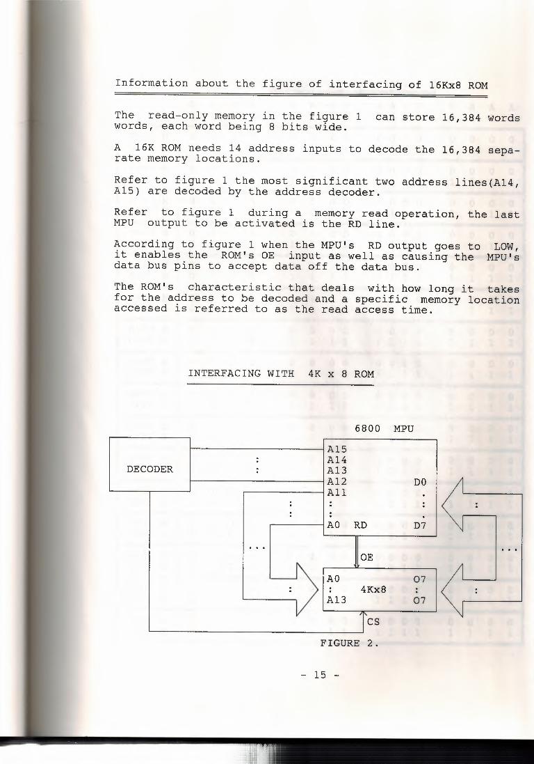
Information about the figure of interfacing of 16Kx8 ROM
The read-only memory in the figure 1 can store 16,384 words words, each word being 8 bits wide.
A 16K ROM needs 14 address inputs to decode the 16,384 sepa rate memory locations.
Refer to figure 1 the most significant two address lines(A14, Al5) are decoded by the address decoder.
Refer to figure 1 during a memory read operation, the last MPU output to be activated is the RD line.
According to figure 1 when the MPU's RD output goes to LOW, it enables the ROM's OE input as well as causing the MPU's data bus pins to accept data off the data bus.
The ROM's characteristic that deals with how long it takes for the address to be decoded and a specific memory location accessed is referred to as the read access time.
INTERFACING WITH 4K x 8 ROM
6800 MPU
Al5 : A14
DECODER : A13 A12 DO All .
: : . . : : .
AO RD D7
... OE
AO 07 : - : 4Kx8 . .
Al3 07 I Tes
FIGURE 2.
- 15 -

A A A A 15 14 13 12
ADDRESS MAP FOR FIGURE 2
A A A A 11 10 9 8
A A A A 7 6 5 4
A A A A 3 2 1 0
0000 H OFFF H
0 0
0 0
0 0 0 0
0 1
0 0 0 1 1 1
0 0 0 0 1 1 1 1
0 0 0 1 1 1
0 1
1000 H lFFF H
2000 H 2FFF H
0 0
0 0
0 0
0 1 0 1
0 1
0 0 0 1 1 1
0 0 0 0 1 1 1 1
0 0 0 0 1 1 1 1
0 0 0 1 1 1
0 0 0 1 1 1
0 1
0 1
3000 H 3FFF H
0 0
0 0
1 0 1 0
0 1
0 0 0 1 1 1
0 0 0 0 1 1 1 1
0 0 0 1 1 1
0 1
4000 H 4FFF H
0 0
0 0
1 1 1 1
0 1
0 0 0 1 1 1
0 0 0 0 1 1 1 1
0 0 0 1 1 1
0 1
5000 H 5FFF H
0 1
0 0
1 1
0 0 0 0
0 1
0 0 0 1 1 1
0 0 0 0 1 1 1 1
0 0 0 1 1 1
6000 H 6FFF H
0 1
0 0
1 1
0 1 0 1
0 1
0 0 0 1 1 1
0 0 0 0 1 1 1 1
0 0 0 1 1 1
7000 H 7FFF H
0 0
1 1
1 0 1 0
0 1
0 0 0 1 1 1
0 0 0 0 1 1 1 1
0 0 0 1 1 1
0 1
8000 H 8FFF H
1 1
1 1
1 1 1 1
0 1
0 0 0 1 1 1
0 0 0 0 1 1 1 1
0 0 0 1 1 1
0 1
9000 H II 1 9FFF H 1
0 1
0 1
0 0
0 0 0 0
0 1
0 0 0 1 1 1
0 0 0 0 1 1 1 1
0 1
0 1
AOOO H II 1 AFFF H 1
0 0 1 0 0 1
0 1 0 0 1 0
0 0 0 0 1 1 1 1
0 0 0 0 1 1 1 1
0 0 0 0 1 1 1 1
0 1
0 1
0 1
0 1
BOOO H I 1 BFFF H 1
COOO H 1 CFFF H 1
0 1 1 0 1 1
0 0 0 0 1 1 1 1
0 0 0 0 1 1 1 1
0 1
0 1
0 1
0 1
1 0 0 1 0 0
0 0 0 0 1 1 1 1
0 0 0 0 1 1 1 1
0 1
0 1
0 1
0 1
DOOO H I 1 DFFF H 1
E()()() R \\ l
EFFF HJ\ 1
1 0 1 1 0 1
l l () 1 1 0
0 0 0 0 1 1 1 1
() () () ()
1 1 1 1
0 0 0 0 1 1 1 1
\) \) \) \) 1 1 1 1
0 1
0 1
0 1
0 1
FOOO H ]~ 1 FFFF H II 1
1 1 1 1 1 1
0 0 0 0 1 1 1 1
- 16 -
0 0 0 0 1 1 1 1
0 1
0 1
0 1 ~ l
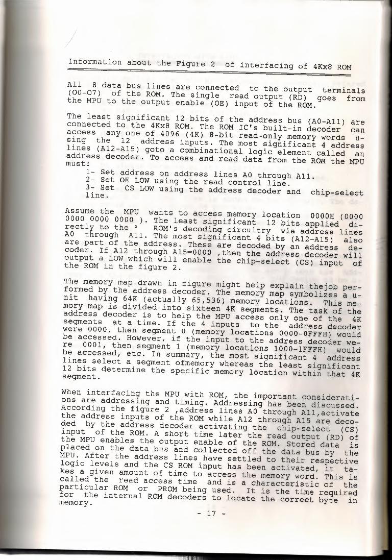
I Information about the Figure 2 of interfacing of 4Kx8 ROM
All 8 data bus lines are connected to the output terminals (00-07) of the ROM. The single read output (RD) goes from the MPU to the output enable (OE) input of the ROM.
The least significant 12 bits of the address bus (AO-All) are connected to the 4Kx8 ROM. The ROM IC's built-in decoder can access any one of 4096 (4K) 8-bit read-only memory words u sing the 12 address inputs. The most significant 4 address lines (Al2-A15) goto a combinational logic element called an address decoder. To access and read data from the ROM the MPU must:
1- Set 2- Set 3- Set line.
address on address lines AO through All. OE LOW using the read control line. CS LOW using the address decoder and chip-select
Assume the MPU wants to access memory location OOOOH (0000 0000 0000 0000 ). The least significant 12 bits applied di rectly to the 2 ROM's decoding circuitry via address lines AO through All. The most significant 4 bits (Al2-Al5) also are part of the address. These are decoded by an address de coder. If Al2 through Al5=0000 ,then the address decoder will output a LOW which will enable the chip-select (CS) input of the ROM in the figure 2.
The memory map drawn in figure might help explain thejob per formed by the address decoder. The memory map symbolizes au nit having 64K (actually 65,536) memory locations. This me mory map is divided into sixteen 4K segments. The task of the address decoder is to help the MPU access only one of the 4K segments at a time. If the 4 inputs to the address decoder were 0000, then segment O (memory locations 0000-0FFFH) would be accessed. However, if the input to the address decoder we re 0001, then segment 1 (memory locations 1000-lFFFH) would be accessed, etc. In summary, the most significant 4 address lines select a segment ofmemory whereas the least significant 12 bits determine the specific memory location within that 4K segment.
- 17 -
When interfacing the MPU with ROM, the important considerati ons are addressing and timing. Addressing has been discussed. According the figure 2 ,address lines AO through All,activate the address inputs of the ROM while Al2 through Al5 are deco ded by the address decoder activating the chip-select (CS) input of the ROM. A short time later the read output (RD) of the MPU enables the output enable of the ROM. Stored data is placed on the data bus and collected off the data bus by the MPU. After the address lines have settled to their respective logic levels and the CS ROM input has been activated, it ta kes a given amount of time to access the memory word. This is called the read access time and is a characteristic of the particular ROM or PROM being used. It is the time required for the internal ROM decoders to locate the correct byte in memory.
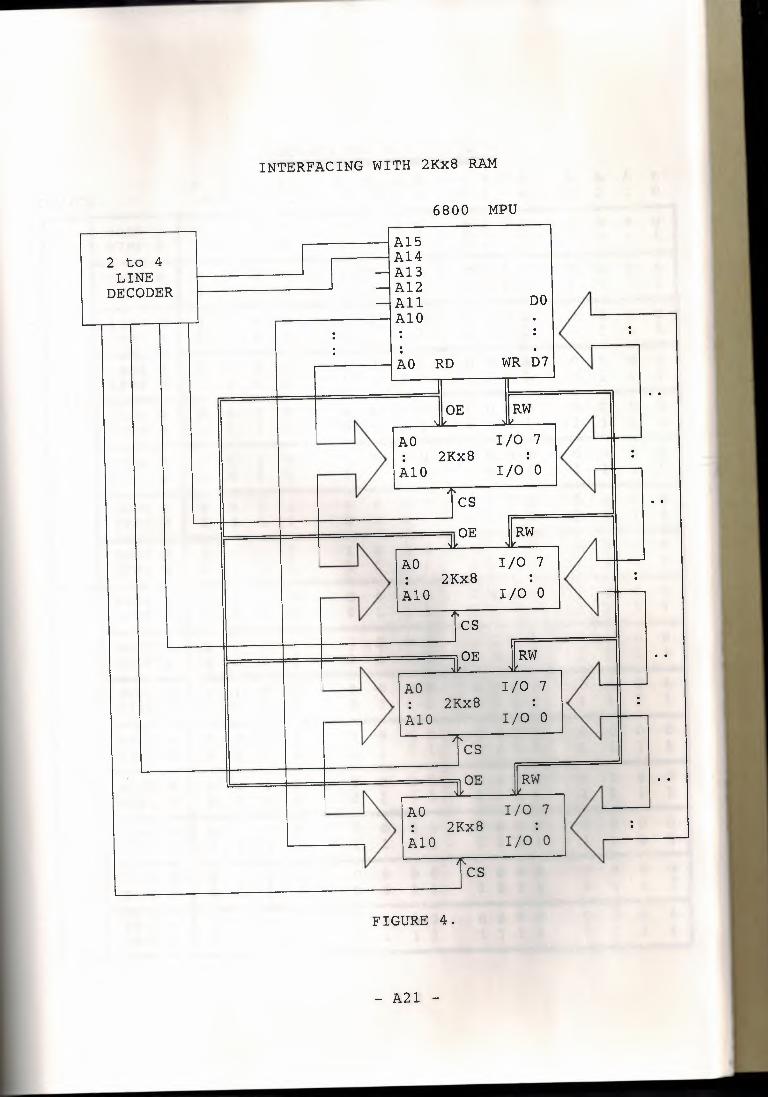
INTERFACING WITH RAM
Read/write devices that the MPU access are commonly refered as RAM. RAM's are divided into 2.
1-) Static RAM characteristics a) Basic elements are the flip flops b) It occupies larger area c) Faster d) It occupies more power to operate
2-) Dynamic Memories (Capacitors) a) Can be constructed densly b) Slower because of its capasitive effects c) Required periodic refreshing. 50 timed/sec.
The interfacing technique is similar to the ROM interface, except that R/W control line is added to the circuit. Theda ta bus could be programmed in two ways. The decoder mechanism works in the same way, such that many RAM modules could be interfaced to the MPU by the module se- lect line (MS).
If we are to write to RAM device, we bring the RD line and the R/W line LOW. The I/0 ports of the RAM are internally programmed as inputs. Hence the MPU selects the data to be written to the required memory location and places the add ress on the address bus. To activate the RAM device to be u sed its selected by address lines A12-Al5. The decoder se lects the appropriate device to be used at the decoder out put. Similarly to read from the RAM, initially WR line is held HIGH so that the I/0 ports of the RAM are programmed as outputs.
Data to be acted on is fetched from the data bus of the RAM, which is selected from the address line inputs. Some discus sions for the expansion of the RAM is also valid for the in terfacing of RAM.
- 18 -
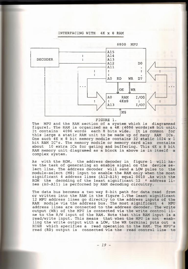
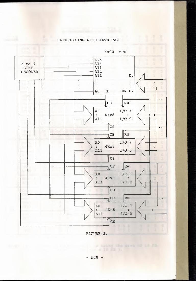
INTERFACING WITH 4K x 8 RAM
6800 MPU
Al5 : A14
DECODER : A13 A12 DO All .
: : : : : .
AO RD WR D7
... OE WR
~ " . AO RAM I/00 : : 4Kx8 . .
A13 I/07
TMS
FIGURE 1. The MPU and the RAM section of a system which is diagrammed figurel. The RAM is organized as a 4K (4096 words)x8 bit unit. It contains 4096 words each 8 bits wide. It is common for this large a static RAM unit to be made up of many RAM res. One such 4K x 8 bit memory module contains 32 static 1024 x 1 bit RAM IC's. The memory module or memory card also contains about 10 extra res for gating and buffering. This 4K x 8 bit RAM memory unit diagramed as a block in above is in itself a complex system.
As with the ROM, the address decoder in figure 1 will ha ve the task of generating an enable signal on the device se lect line. The address decoder will send a LOW pulse to the module-select (MS) input to enable the RAM only when the most significant 4 address lines (Al2-Al5) equal 0010 .As with the ROM the decoding of the least significant 12 2 address li nes (AO-All) is performed by RAM decoding circuitry.
The data bus becomes a two way 8-bit path for data read from or written into the RAM in the figure 1.The least significant 12 MPU address lines go directly to the address inputs of the RAM module via the address bus. The most significant 4 MPU address lines are connected to the address decoder. The write output (WR) of the MPU is connected via the write control li ne to the R/W input of the RAM. Note that this RAM input is a read/write input. This means that when the MPU is not enab ling the write output with a LOW, the WR terminal puts out a HIGH which specifies a read operation to the RAM. The MPU's read (RD) output is connected via the read control line to
- 19 -

the output enable (OE) of the RAM. A LOW on the read control line will enable the outputs of the RAM module.
~DDRESS MAP FOR FIGURE 1
A A A A 15 14 13 12
A A A A 11 10 9 8
A A A A 7 6 5 4
A A A A 3 2 1 0
0000 H I g 0 0 0 0 0 0 0 0 0 0 0 0 0 0 ~ I OFFF H 0 0 0 1 1 1 1 1 1 1 1 1 1 1
1000 H I g 0 0 1 0 0 0 0 0 0 0 0 0 0 0 ~ I lFFF H 0 0 1 1 1 1 1 1 1 1 1 1 1 1
2000 H I g
0 1 0 0 0 0 0 0 0 0 0 0 0 0 ~ I 2FFF H 0 1 0 1 1 1 1 1 1 1 1 1 1 1
3000 H I g 0 1 1 0 0 0 0 0 0 0 0 0 0 0
~ I 3FFF H 0 1 1 1 1 1 1 1 1 1 1 1 1 1
4000 H I g 1 0 0 0 0 0 0 0 0 0 0 0 0 0 ~ I 4FFF H 1 0 0 1 1 1 1 1 1 1 1 1 1 1
5000 H I g 1 0 1 0 0 0 0 0 0 0 0 0 0 0
~ I 5FFF H 1 0 1 1 1 1 1 1 1 1 1 1 1 1
6000 H I g 1 1 0 0 0 0 0 0 0 0 0 0 0 0 ~ I 6FFF H 1 1 0 1 1 1 1 1 1 1 1 1 1 1
7000 H I g 1 1 1 0 0 0 0 0 0 0 0 0 0 0
~ I 7FFF H 1 1 1 1 1 1 1 1 1 1 1 1 1 1
8000 H I i 0 0 0 0 0 0 0 0 0 0 0 0 0 0 ~ I 8FFF H 0 0 0 1 1 1 1 1 1 1 1 1 1 1
9000 H
I
1 0 0 1 0 0 0 0 0 0 0 0 0 0 0 ~ I 9FFF H 1 0 0 1 1 1 1 1 1 1 1 1 1 1 1
AOOO H I 1 0 1 0 0 0 0 0 0 0 0 0 0 0 0 ~ I 0 1 0 1 1 1 1 1 1 1 1 1 1 1 AFFF H 1
BOOO H I i 0 1 1 0 0 0 0 0 0 0 0 0 0 0
~ I BFFF H 0 1 1 1 1 1 1 1 1 1 1 1 1 1
COOO H I i 1 0 0 0 0 0 0 0 0 0 0 0 0 0
~ I CFFF H 1 0 0 1 1 1 1 1 1 1 1 1 1 1
D000 H I i 1 0 1 0 0 0 o- 0 0 0 0 0 0 0
~ I DFFF H 1 0 1 1 1 1 1 1 1 1 1 1 1 1
EOOO H
I
1 1 1 0 0 0 0 0 0 0 0 0 0 0 0 ~ I EFFF H 1 1 1 0 1 1 1 1 1 1 1 1 1 1 1
FOOO H I i 1 1 1 0 0 0 0 0 0 0 0 0 0 0
~ I FFFF H 1 1 1 1 1 1 1 1 1 1 1 1 1 1
- 20 -

The MPU's address lines are set\to a valid address, and then the read output(RD) goes LOW. \The data bus goes from a tree-state to an input condition. The MPU is ready to accept data of the data bus. The RAM's module select(MS) and output enable (OE) inputs are both driven LOW or enabled by the address decoder and the read control line from the MPU. The read/write(R/W) input is held HIGH or in the read mode. Shortly after the output enable (OE) goes LOW, the data out puts are activated. Stored data is placed on the data bus by the outputs of the RAM. As on a ROM, the read access time is an important characteristic of the RAM. The maximum read access time might range from 250 to 1000 ns for common static RAMs.
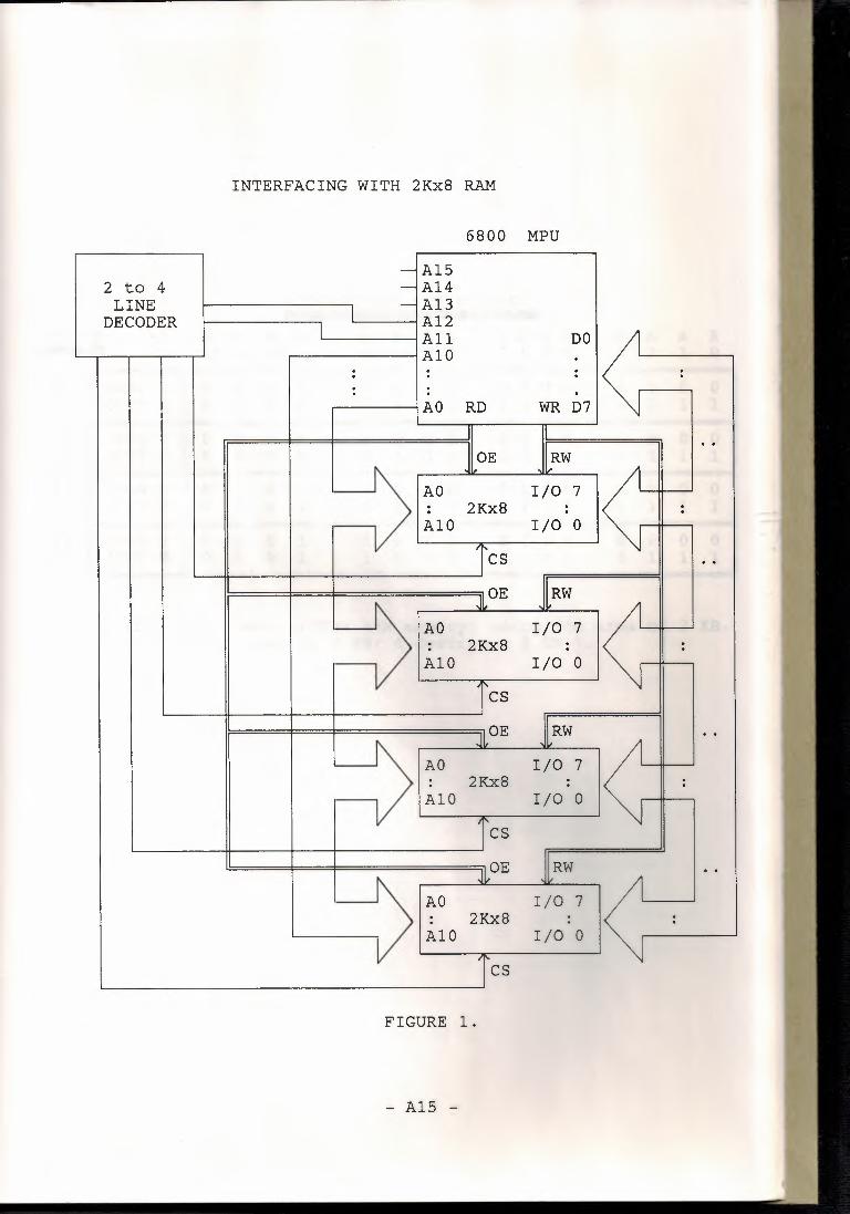
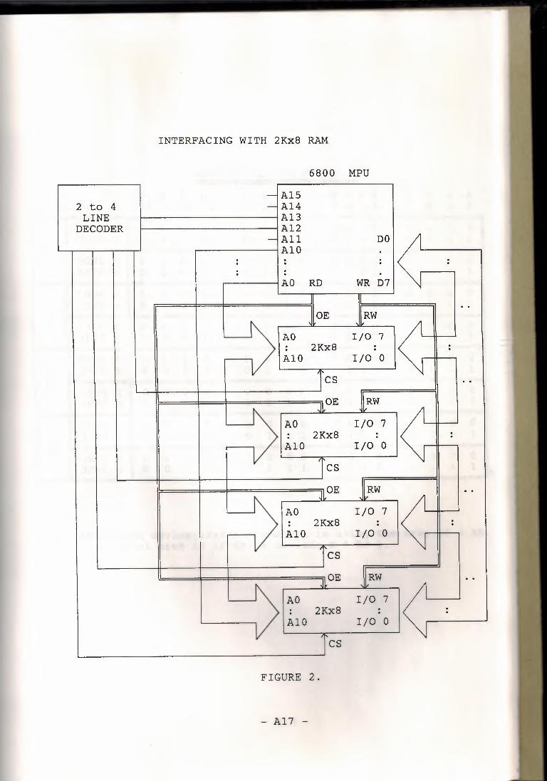
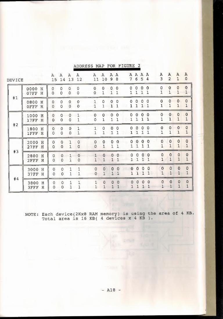
INTERFACING WITH 2K x 8 RAM
6800 MPU
Al5 : Al4
DECODER : Al3 : Al2
All DO AlO .
: : : . : . . AO RD WR D7
... OE WR
I
=>AO RAM I/00
l10 2Kx8 . .
I/07
Tes
FIGURE 2.
The MPU and the RAM section of a system which is diagrammed in the figure 2. The RAM is organized as a 2K (2048 words)x8 bit unit. It contains 2048 words each 8 bits wide. It is com mon for this large a static RAM unit to be made up of many RAM res. One such 2K x 8 bit memory module contains 32 static 1024 x 1 bit RAM IC's. The memory module or memory card also contains about 10 extra res for gating and buffering. This 2K x 8-bit RAM memory unit diagrammed as a block in figure 2 is in itself a complex system.
As with the ROM, the address decoder in figure 2 will ha ve the task of generating an enable signal on the device se lect line. The address decoder will send a LOW pulse to the
- 21 -

module-select (MS) input to enable the RAM only when the most significant 5 address lines (All-Al5) equal 0010 .As with the ROM the decoding of the least significant 11 2 address li nes (AO-AlO) is performed by RAM decoding circuitry.
The data bus becomes a two way 8-bit path for data read from or written into the RAM in the figure 2.The least significant 11 MPU address lines go directly to the address inputs of the RAM module via the address bus. The most significant 5 MPU address lines are connected to the address decoder. The write output (WR) of the MPU is connected via the write control li ne to the R/W input of the RAM. Note that this RAM input is a read/write input. This means that when the MPU is not enab ling the write output with a LOW, the WR terminal puts out a HIGH which specifies a read operation to the RAM. The MPU's read (RD) output is connected via the read control line to the output enable (OE) of the RAM. A LOW on the read control line will enable the outputs of the RAM module.
A7 1 24 Vee
A6 2 23 AS
AS 3 22 A9
A4 4 21 WE
A3 5 2K X 8 20 OE
A2 6 RAM 19 AlO
Al 7 18 cs AO 8 17 I/0 8
6 1 1 6 I/0 1 9 16 I/0 7
I/0 2 10 15 I/0 6
I/0 3 11 STATIC 14 I/0 5
GN 12 13 I/0 4
PIN DIAGRAM OF 2K x 8 RAM.
- 22 -

ADDRESS MAP FOR FIGURE 2
A A A A 15 14 13 12
A A A A 11 10 9 8
A A A A 7 6 5 4
A A A A 3 2 1 0
0000 H I ~
0 0 0 0 0 0 0 0 0 0 0 0 0 0 ~ I 07FF H 0 0 0 0 1 1 1 1 1 1 1 1 1 1
0800 H I ~ 0 0 0 1 0 0 0 0 0 0 0 0 0 0 ~ I OFFF H 0 0 0 1 1 1 1 1 1 1 1 1 1 1
1000 H 0 0 0 1 0 0 0 0 0 0 0 0 0 0 0 0 17FF H 0 0 0 1 0 1 1 1 1 1 1 1 1 1 1 1
1800 H 0 0 0 1 1 0 0 0 0 0 0 0 0 0 0 0 lFFF H 0 0 0 1 1 1 1 1 1 1 1 1 1 1 1 1
2000 H 0 0 1 0 0 0 0 0 0 0 0 0 0 0 0 0 27FF H 0 0 1 0 0 1 1 1 1 1 1 1 1 1 1 1
2800 H 0 0 1 0 1 0 0 0 0 0 0 0 0 0 0 0 2FFF H 0 0 1 0 1 1 1 1 1 1 1 1 1 1 1 1
3000 H 0 0 1 1 0 0 0 0 0 0 0 0 0 0 0 0 37FF H 0 0 1 1 0 1 1 1 1 1 1 1 1 1 1 1
3800 H 0 0 1 1 1 0 0 0 0 0 0 0 0 0 0 0 3FFF H 0 0 1 1 1 1 1 1 1 1 1 1 1 1 1 1
4000 H I ~ 1 0 0 0 0 0 0 0 0 0 0 0 0 0 ~ I 47FF H 1 0 0 0 1 1 1 1 1 1 1 1 1 1
4800 H I ~
1 0 0 1 0 0 0 0 0 0 0 0 0 0 ~ I 4FFF H 1 0 0 1 1 1 1 1 1 1 1 1 1 1
5000 H I ~ 1 0 1 0 0 0 0 0 0 0 0 0 0 0 ~ I 57FF H· 1 0 1 0 1 1 1 1 1 1 1 1 1 1
5800 H 0 1 0 1 1 0 0 0 0 0 0 0 0 0 0 0 5FFF H 0 1 0 1 1 1 1 1 1 1 1 1 1 1 1 1
6000 H 0 1 1 0 0 0 0 0 0 0 0 0 0 0 0 0 67FF H 0 1 1 0 0 1 1 1 1 1 1 1 1 1 1 1
6800 H 0 1 1 0 1 0 0 0 0 0 0 0 0 0 0 0 6FFF H 0 1 1 0 1 1 1 1 1 1 1 1 1 1 1 1
7000 H 0 1 1 1 0 0 0 0 0 0 0 0 0 0 0 0 77FF H 0 1 1 1 0 1 1 1 1 1 1 1 1 1 1 1
7800 H I ~
1 1 1 1 0 0 0 0 0 0 0 0 0 0 0 7FFF H 1 1 1 1 1 1 1 1 1 1 1 1 1 1 1
- 23 -

A A A A 15 14 13 12
A A A A 11 10 9 8
A A A A 7 6 5 4
A A A A 3 2 1 0
8000 H 1 0 0 0 0 0 0 0 0 0 0 0 0 0 0 0 87FF H 1 0 0 0 0 1 1 1 1 1 1 1 1 1 1 1
8800 H 1 0 0 0 1 0 0 0 0 0 0 0 0 0 0 0 8FFF H 1 0 0 0 1 1 1 1 1 1 1 1 1 1 1 1
9000 H 1 0 0 1 0 0 0 0 0 0 0 0 0 0 0 0 97FF H 1 0 0 1 0 1 1 1 1 1 1 1 1 1 1 1
9800 H 1 0 0 1 1 0 0 0 0 0 0 0 0 0 0 0 9FFF H 1 0 0 1 1 1 1 1 1 1 1 1 1 1 1 1
AOOO H 1 0 1 0 0 0 0 0 0 0 0 0 0 0 0 0 A7FF H 1 0 1 0 0 1 1 1 1 1 1 1 1 1 1 1
A800 H 1 0 1 0 1 0 0 0 0 0 0 0 0 0 0 0 AFFF H 1 0 1 0 1 1 1 1 1 1 1 1 1 1 1 1
BODO H
I 1 0 1 1 0 0 0 0 0 0 0 0 0 0 0 0
B7FF H 1 0 1 1 0 1 1 1 1 1 1 1 1 1 1 1
B800 H 1 0 1 1 1 0 0 0 0 0 0 0 0 0 0 0 BFFF H 1 0 1 1 1 1 1 1 1 1 1 1 1 1 1 1
COOO H 1 1 0 0 0 0 0 0 0 0 0 0 0 0 0 0 C7FF H 1 1 0 0 0 1 1 1 1 1 1 1 1 1 1 1
C800 H 1 1 0 0 1 0 0 0 0 0 0 0 0 0 0 0 CFFF H 1 1 0 0 1 1 1 1 1 1 1 1 1 1 1 1
DODO H 1 1 0 1 0 0 0 0 0 0 0 0 0 0 0 0 D7FF H 1 1 0 1 0 1 1 1 1 1 1 1 1 1 1 1
D800 H I i 1 0 1 1 0 0 0 0 0 0 0 0 0 0 ~ I DFFF H 1 0 1 1 1 1 1 1 1 1 1 1 1 1
EOOO H I t 1 1 0 0 0 0 0 0 0 0 0 0 0 0 ~ I E7FF H 1 1 0 0 1 1 1 1 1 1 1 1 1 1
E800 H I t 1 1 0 1 0 0 0 0 0 0 0 0 0 0 ~ I EFFF H 1 1 0 1 1 1 1 1 1 1 1 1 1 1
FOOO H I t 1 1 1 0 0 0 0 0 0 0 0 0 0 0 ~ I F7FF H 1 1 1 0 1 1 1 1 1 1 1 1 1 1
F800 H ( i 1 1 1 1 0 0 0 0 0 0 0 0 0 0 q FFFF H 1 1 1 1 1 1 1 1 1 1 1 1 1 1
- 24 -
- 25 -
C O N C L U S I O N
After the successfull interfacing of devices (ROMs or RAM)s, the microprocessor can read/write to/from memories(ROMs or RAMs). We can interface more memory units to the MPU then its maximum capacity. By using a decoder we could select any memory unit to be interfaced to the MPU providing easy access to all memory units.

A P P E N D I X A

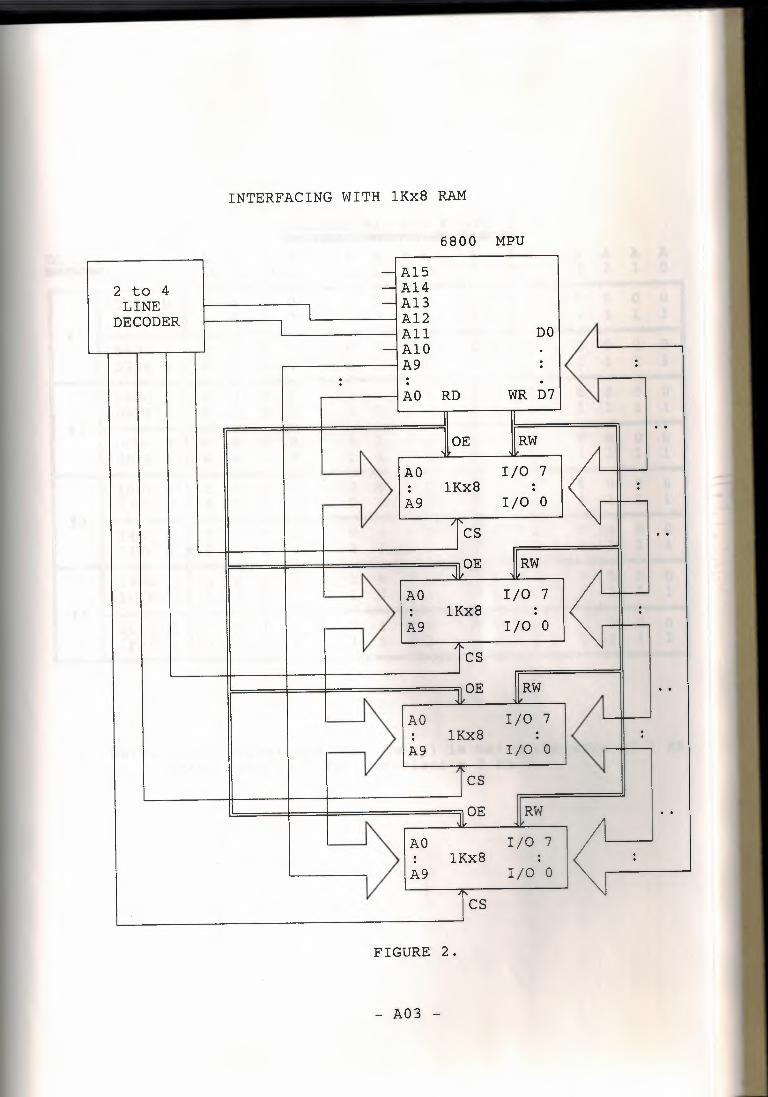
INTERFACING WITH 1Kx8 RAM
6800 MPU
- Al5 2 to 4 - Al4 LINE
I - Al3
DECODER
I - Al2
All DO AlO . A9 : . .
: : . AO RD WR D7
.. OE RW
' 'I,
~ ~o I/0 7
1Kx8 : . . A9 I/0 0
Tes .. J~OE RW
AO I/0 7 : 1Kx8 . . . . A9 I/0 0
Tes J~OE RW ..
AO I/0 7 : 1Kx8 . . . . A9 I/0 0
Tes l~OE RW ..
AO I/0 7 : 1Kx8 : : A9 I/0 0
Tes FIGURE 1.
- AOl -

DEVICE
#1
#2
#3
#4
ADDRESS MAP FOR FIGURE 1
A A A A 3 2 1 0 A A A A
15 14 13 12 A A A A 11 10 9 8
A A A A 7 6 5 4
0000 H I g 0 0 0 0 0 0 0 0 0 0 0 0 0 0 ~ I 03FF H 0 0 0 0 0 1 1 1 1 1 1 1 1 1
0400 H I g 0 0 0 0 1 0 0 0 0 0 0 0 0 0 ~ I 07FF H 0 0 0 0 1 1 1 1 1 1 1 1 1 1
0800 H I g 0 0 0 1 0 0 0 0 0 0 0 0 0 0 ~ I OBFF H 0 0 0 1 0 1 1 1 1 1 1 1 1 1
ocoo H I 0 0 0 0 1 1 0 0 0 0 0 0 0 0 0 ~ I 0 0 0 1 1 1 1 1 1 1 1 1 1 1 OFFF H 0
NOTE: Each device(1Kx8 RAM memory) is using the area of 1 KB. Total area is 4 KB (4 devices x 1 KB).
- A02 -
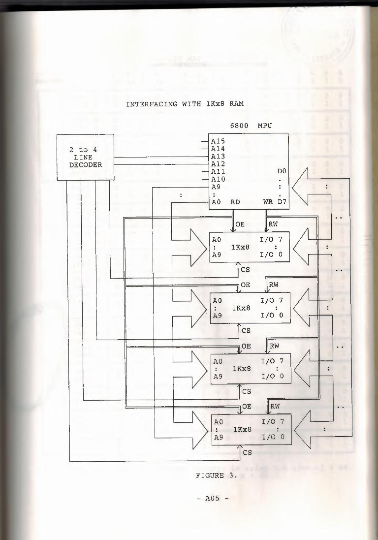
INTERFACING WITH 1Kx8 RAM
6800 MPU
- Al5 2 to 4 - Al4 LINE I - Al3
DECODER Al2 All DO
- AlO . A9 : : . . . . . AO RD WR D7
.. OE RW
' ,i,
AO I/0 7 : 1Kx8 . : . A9 I/0 0
T cs .. ,ll,OE RW
AO I/0 7 : 1Kx8 . : . A9 I/0 0
Tes lLOE RW ..
AO I/0 7 : 1Kx8 : : A9 I/0 0
Tes .II.OE RW ..
AO I/0 7 : 1Kx8 : . . A9 I/0 0
Tes FIGURE 2.
- A03 -
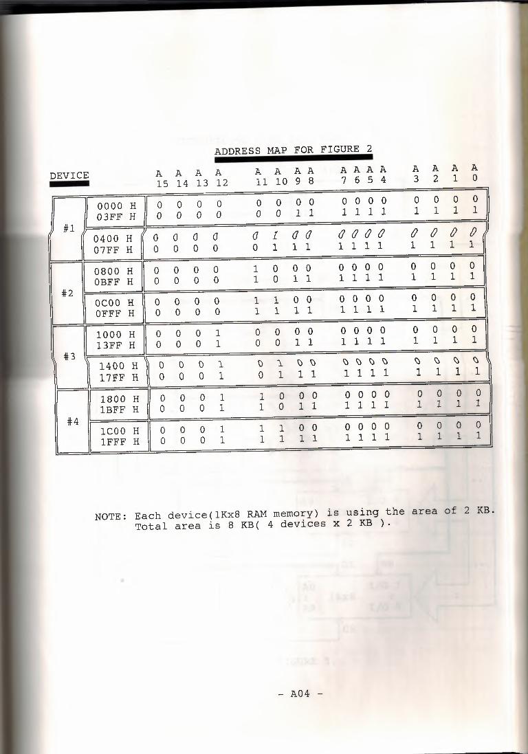
ADDRESS MAP FOR FIGURE 2
DEVICE A A A A 15 14 13 12
A A A A 11 10 9 8
A A A A 7 6 5 4
A A A A 3 2 1 0
0000 H I g 0 0 0 0 0 0 0 0 0 0 0 0 0 0 ~ I 03FF H 0 0 0 0 0 1 1 1 1 1 1 1 1 1
#1 ( ~ r I 0400 H 0 0 a (] I (] (] (l (l (l (l (} (} (}
07FF H 0 0 0 0 1 1 1 1 1 1 1 1 1 1
0800 H I g 0 0 0 1 0 0 0 0 0 0 0 0 0 0 ~ I OBFF H 0 0 0 1 0 1 1 1 1 1 1 1 1 1
#2 ocoo H I 0 0 0 0 1 1 0 0 0 0 0 0 0 0 0 ~ l 0 0 0 1 1 1 1 1 1 1 1 1 1 1 OFFF H 0
1000 H I g 0 0 1 0 0 0 0 0 0 0 0 0 0 0 ~ I 13FF H 0 0 1 0 0 1 1 1 1 1 1 1 1 1
4\:3 1400 Ht 0 () () 1. \) 1. \) \) \) \) \) \) \) \) \)
~ J 0 0 1 0 1 1 1 1 1 1 1 1 1 1 17FF H 0 I
1800 H I g 0 0 1 1 0 0 0 0 0 0 0 0 0 0 f I lBFF H 0 0 1 1 0 1 1 1 1 1 1 1 1 1
#4 lCOO H I g
0 0 1 1 1 0 0 0 0 0 0 0 0 0 ~ I lFFF H 0 0 1 1 1 1 1 1 1 1 1 1 1 1
NOTE: Each device(1Kx8 RAM memory) is using the area of 2 KB. Total area is 8 KB( 4 devices x 2 KB) .
•
- A04 -
INTERFACING WITH 1Kx8 RAM
6800 MPU
- Al5 2 to 4 - Al4 LINE Al3
DECODER Al2 - All DO - AlO .
A9 : : : : .
AO RD WR D7
.. OE RW
' 1,
AO I/0 7 : 1Kx8 : : A9 I/0 0
Tes .. JLOE RW
AO I/0 7 : 1Kx8 : . . A9 I/0 0
Tes ];OE j RW ..
AO I/0 7 : 1Kx8 : . . A9 I/0 0
Tes 11,0E l,RW ..
AO I/0 7 : 1Kx8 : : A9 I/0 0
Tes FIGURE 3.
- A05 -

ADDRESS MAP FOR FIGURE 3
DEVICE A A A A 15 14 13 12
A A A A 11 10 9 8
A A A A 7 6 5 4
A 0
0000 H I g
0 0 0 0 0 0 0 0 0 0 0 0 0 0 ~ I 03FF H 0 0 0 0 0 1 1 1 1 1 1 1 1 1
0400 H I g
0 0 0 0 1 0 0 0 0 0 0 0 0 0 ~ I 07FF H 0 0 0 0 1 1 1 1 1 1 1 1 1 1
#1 0800 H
I ~
0 0 0 1 0 0 0 0 0 0 0 0 0 0 ~ I OBFF H 0 0 0 1 0 1 1 1 1 1 1 1 1 1
OCOO H I g
0 0 0 1 1 0 0 0 0 0 0 0 0 0 ~ I OFFF H 0 0 0 1 1 1 1 1 1 1 1 1 1 1
1000 H I g
0 0 1 0 0 0 0 0 0 0 0 0 0 0 ~ I 13FF H 0 0 1 0 0 1 1 1 1 1 1 1 1 1
1400 H I g
0 0 1 0 1 0 0 0 0 0 0 0 0 0 ~ I 17FF H 0 0 1 0 1 1 1 1 1 1 1 1 1 1
#2 1800 H
I g 0 0 1 1 0 0 0 0 0 0 0 0 0 0
~ I lBFF .H 0 0 1 1 0 1 1 1 1 1 1 1 1 1
lCOO H
I 0 0 0 1 1 1 0 0 0 0 0 0 0 0 0
~ I lFFF H 0 0 0 1 1 1 1 1 1 1 1 1 1 1 1
2000 H I g
0 1 0 0 0 0 0 0 0 0 0 0 0 0 ~ I 23FF H 0 1 0 0 0 1 1 1 1 1 1 1 1 1
2400 H I g
0 1 0 0 1 0 0 0 0 0 0 0 0 0 ~ I 27FF H 0 1 0 0 1 1 1 1 1 1 1 1 1 1
#3 2800 H
I g 0 1 0 1 0 0 0 0 0 0 0 0 0 0
~ I 2BFF H 0 1 0 1 0 1 1 1 1 1 1 1 1 1
2COO H I g
0 1 0 1 1 0 0 0 0 0 0 0 0 0 ~ I 2FFF H 0 1 0 1 1 1 1 1 1 1 1 1 1 1
3000 H I g
0 1 1 0 0 0 0 0 0 0 0 0 0 0 ~ I 33FF H 0 1 1 0 0 1 1 1 1 1 1 1 1 1
3400 H I g
0 1 1 0 1 0 0 0 0 0 0 0 0 0 ~ I 37FF H 0 1 1 0 1 1 1 1 1 1 1 1 1 1
#4 3800 H
I g 0 1 1 1 0 0 0 0 0 0 0 0 0 0 ~ I 3BFF H 0 1 1 1 0 1 1 1 1 1 1 1 1 1
3COO H I g
0 1 1 1 1 0 0 0 0 0 0 0 0 0 ~ I 3FFF H 0 1 1 1 1 1 1 1 1 1 1 1 1 1
NOTE: Each device(1Kx8 RAM memory) is using the area of 4 KB. Total area is 16 KB( 4 devices x 4 KB).
- A06 -

INTERFACING WITH 1Kx8 RAM
6800 MPU
- Al5 2 to 4 I Al4 LINE I Al3
DECODER - Al2 - All DO - AlO .
A9 . . . . : . . .
AO RD WR D7
.. OE RW
' I,
AO I/0 7 : 1Kx8 . : . A9 I/0 0
Tes .. J~OE Jl,Rw
AO I/0 7 : 1Kx8 : : A9 I/0 0
Tes JLOE J RW ..
AO I/0 7 : 1Kx8 . : . A9 I/0 0
1 cs Jl,OE RW ..
AO I/0 7 : 1Kx8 : : A9 I/0 0
fcs FIGURE 4.
- A07 -

ADDRESS MAP FOR FIGURE 4
DEVICE A A A A 15 14 13 12
A A A A 11 10 9 8
A A A A 7 6 5 4
A A A A 3 2 1 0
0000 H I g
0 0 0 0 0 0 0 0 0 0 0 0 0 0 ~ I 03FF H 0 0 0 0 0 1 1 1 1 1 1 1 1 1
0400 H I g
0 0 0 0 1 0 0 0 0 0 0 0 0 0 ~ I 07FF H 0 0 0 0 1 1 1 1 1 1 1 1 1 1
0800 H I g
0 0 0 1 0 0 0 0 0 0 0 0 0 0 ~ I OBFF H 0 0 0 1 0 1 1 1 1 1 1 1 1 1
OCOO H I g
0 0 0 1 1 0 0 0 0 0 0 0 0 0 ~ I OFFF H 0 0 0 1 1 1 1 1 1 1 1 1 1 1
#1
I g ~ I
1000 H 0 0 1 0 0 0 0 0 0 0 0 0 0 0 13FF H 0 0 1 0 0 1 1 1 1 1 1 1 1 1
1400 H I g 0 0 1 0 1 0 0 0 0 0 0 0 0 0
~ I 17FF H 0 0 1 0 1 1 1 1 1 1 1 1 1 1
1800 H I g
0 0 1 1 0 0 0 0 0 0 0 0 0 0 ~ I lBFF H 0 0 1 1 0 1 1 1 1 1 1 1 1 1
lCOO H I 0 0 0 1 1 1 0 0 0 0 0 0 0 0 0 ~ I 0 0 1 1 1 1 1 1 1 1 1 1 1 1 lFFF H 0
2000 H I g
0 1 0 0 0 0 0 0 0 0 0 0 0 0 ~ I 23FF H 0 1 0 0 0 1 1 1 1 1 1 1 1 1
2400 H I g 0 1 0 0 1 0 0 0 0 0 0 0 0 0
~ I 27FF H 0 1 0 0 1 1 1 1 1 1 1 1 1 1
2800 H I g
0 1 0 1 0 0 0 0 0 0 0 0 0 0 ~ I 2BFF H 0 1 0 1 0 1 1 1 1 1 1 1 1 1
2COO H I g
0 1 0 1 1 0 0 0 0 0 0 0 0 0 ~ I 2FFF H 0 1 0 1 1 1 1 1 1 1 1 1 1 1
#2 3000 H I g
0 1 1 0 0 0 0 0 0 0 0 0 0 0 ~ I 33FF H 0 1 1 0 0 1 1 1 1 1 1 1 1 1
3400 H I g
0 1 1 0 1 0 0 0 0 0 0 0 0 0 ~ I 37FF H 0 1 1 0 1 1 1 1 1 1 1 1 1 1
3800 H I g
0 1 1 1 0 00 0 0 0 0 0 0 0 ~ I 3BFF H 0 1 1 1 0 1 1 1 1 1 1 1 1 1
3COO H I g
0 1 1 1 1 0 0 0 0 0 0 0 0 0 ~ I 3FFF H 0 1 1 1 1 1 1 1 1 1 1 1 1 1
- A08 -
DEVICE A A A A 15 14 13 12
A A A A 11 10 9 8
A A A A 7 6 5 4
A A A A 3 2 1 0
4000 H I g 1 0 0 0 0 0 0 0 0 0 0 0 0 0
~ I 43FF H 1 0 0 0 0 1 1 1 1 1 1 1 1 1
4400 H I g
1 0 0 0 1 0 0 0 0 0 0 0 0 0 ~ I 47FF H 1 0 0 0 1 1 1 1 1 1 1 1 1 1
4800 H I g 1 0 0 1 0 0 0 0 0 0 0 0 0 0
~ I 4BFF H 1 0 0 1 0 1 1 1 1 1 1 1 1 1
4COO H I g 1 0 0 1 1 0 0 0 0 0 0 0 0 0
~ I 4FFF H 1 0 0 1 1 1 1 1 1 1 1 1 1 1 #3
5000 H I g
1 0 1 0 0 0 0 0 0 0 0 0 0 0 ~ I 53FF H 1 0 1 0 0 1 1 1 1 1 1 1 1 1
5400 H I g
1 0 1 0 1 0 0 0 0 0 0 0 0 0 ~ I 57FF H 1 0 1 0 1 1 1 1 1 1 1 1 1 1
5800 H I g
1 0 1 1 0 0 0 0 0 0 0 0 0 0 ~ I 5BFF H 1 0 1 1 0 1 1 1 1 1 1 1 1 1
5COO H I g
1 0 1 1 1 0 0 0 0 0 0 0 0 0 ~ I 5FFF H 1 0 1 1 1 1 1 1 1 1 1 1 1 1
6000 H
I
0 1 1 0 0 0 0 0 0 0 0 0 0 0 0 ~ I 63FF H 0 1 1 0 0 0 1 1 1 1 1 1 1 1 1
6400 H I g 1 1 0 0 1 0 0 0 0 0 0 0 0 0
~ I 67FF H 1 1 0 0 1 1 1 1 1 1 1 1 1 1
6800 H I g
1 1 0 1 0 0 0 0 0 0 0 0 0 0 ~ I 6BFF H 1 1 0 1 0 1 1 1 1 1 1 1 1 1
6COO H I g
1 1 0 1 1 0 0 0 0 0 0 0 0 0 ~ I 6FFF H 1 1 0 1 1 1 1 1 1 1 1 1 1 1
#4 7000 H
I g 1 1 1 0 0 0 0 0 0 0 0 0 0 0
~ I 73FF H 1 1 1 0 0 1 1 1 1 1 1 1 1 1
7400 H I g 1 1 1 0 1 0 0 0 0 0 0 0 0 0 ~ I 77FF H 1 1 1 0 1 1 1 1 1 1 1 1 1 1
7800 H
I
0 1 1 1 1 0 0 0 0 0 0 0 0 0 0 ~ I 7BFF H 0 1 1 1 1 0 1 1 1 1 1 1 1 1 1
7COO H I g
1 1 1 1 1 0 0 0 0 0 0 0 0 0 ~ I 7FFF H 1 1 1 1 1 1 1 1 1 1 1 1 1 1
NOTE: Each device(1Kx8 RAM memory) is using the area of 8 KB. Total area is 32 KB( 4 devices x 8 KB).
- A09 -
6800 MPU
INTERFACING WITH 1Kx8 RAM
Al5
\ 2 to 4 I Al4
LINE - Al3
DECODER - Al2 - All DO - AlO .
A9 : : : : . I:
AO RD WR D7
.. OE RW
• L ',. AO I/0 7 : 1Kx8 . . . . A9 I/0 0
Tes .. .II.OE RW
AO I/0 7 : 1Kx8 . . . . A9 I/0 0
Tes JLOE RW ..
AO I/0 7 : 1Kx8 . . . . A9 I/0 0
Tes Jl,OE RW ..
~ ~o I/0 7
1Kx8 : : A9 I/0 0
Tes FIGURE 5.
- AlO -
ADDRESS MAP FOR FIGURE 5
A A A A 3 2 1 0 DEVICE A A A A
15 14 13 12 A A A A 11 10 9 8
A A A A 7 6 5 4
0000 H I g 0 0 0 0 0 0 0 0 0 0 0 0 0 0 ~ I 03FF H 0 0 0 0 0 1 1 1 1 1 1 1 1 1
0400 H I g 0 0 0 0 1 0 0 O O O 0 0 0 0 ~ I 07FF H 0 0 0 0 1 1 1 1 1 1 1 1 1 1
0800 H ~ 0 () () () l I.) I.) I.) I.) I.) I.) I.) \) \) \)
~ ~ () () () l () l l l l l l l l l OBFF H ()
OCOO H l g 0 0 0 1 1 0 0 0 0 0 0 0 0 0 ~ I OFFF H 0 0 0 1 1 1 1 1 1 1 1 1 1 1
1000 H I i 0 0 1 0 0 0 0 0 0 0 0 0 0 0 ~ I 13FF H 0 0 1 0 0 1 1 1 1 1 1 1 1 1
1400 H I g 0 0 1 0 1 0 0 0 0 0 0 0 0 0 ~ I 17FF H 0 0 1 0 1 1 1 1 1 1 1 1 1 1
1800 H I g 0 0 1 1 0 0 0 0 0 0 0 0 0 0 ~ I lBFF H 0 0 1 1 0 1 1 1 1 1 1 1 1 1
lCOO H I g 0 0 1 1 1 0 0 0 0 0 0 0 0 0 ~ I lFFF H 0 0 1 1 1 1 1 1 1 1 1 1 1 1
#1 I g ~ I 2000 H 0 1 0 0 0 0 0 0 0 0 0 0 0 0
23FF H 0 1 0 0 0 1 1 1 1 1 1 1 1 1
2400 H I g 0 1 0 0 1 0 0 0 0 0 0 0 0 0 ~ I 27FF H 0 1 0 0 1 1 1 1 1 1 1 1 1 1
2800 H I g 0 1 0 1 0 0 0 0 0 0 0 0 0 0 ~ I 2BFF H 0 1 0 1 0 1 1 1 1 1 1 1 1 1
2COO H I g 0 1 0 1 1 0 0 0 0 0 0 0 0 0 ~ I 2FFF H 0 1 0 1 1 1 1 1 1 1 1 1 1 1
3000 H I g 0 1 1 0 0 0 0 0 0 0 0 0 0 0 ~ I 33FF H 0 1 1 0 0 1 1 1 1 1 1 1 1 1
3400 H I g
0 1 1 0 1 0 0 0 0 0 0 0 0 0 ~ I 37FF H 0 1 1 0 1 1 1 1 1 1 1 1 1 1
3800 H I g 0 1 1 1 0 0 0 0 0 0 0 0 0 0 ~ I 3BFF H 0 1 1 1 0 1 1 1 1 1 1 1 1 1
3COO H I g 0 1 1 1 1 0 0 0 0 0 0 0 0 0 ~ I 3FFF H 0 1 1 1 1 1 1 1 1 1 1 1 1 1
- All -
DEVICE A A A A 15 14 13 12
A A A A 11 10 9 8
A A A A 7 6 5 4
A A A A 3 2 1 0
4000 H I ~
1 0 0 0 0 0 0 0 0 0 0 0 0 0 ~ I 43FF H 1 0 0 0 0 1 1 1 1 1 1 1 1 1
4400 H I ~
1 0 0 0 1 0 0 0 0 0 0 0 0 0 ~ I 47FF H 1 0 0 0 1 1 1 1 1 1 1 1 1 1
4800 H I ~
1 0 0 1 0 0 0 0 0 0 0 0 0 0 ~ I 4BFF H 1 0 0 1 0 1 1 1 1 1 1 1 1 1
4COO H I 0 1 0 0 1 1 0 0 0 0 0 0 0 0 0 ~ I 1 0 0 1 1 1 1 1 1 1 1 1 1 1 4FFF H 0
5000 H I ~
1 0 1 0 0 0 0 0 0 0 0 0 0 0 ~ I 53FF H 1 0 1 0 0 1 1 1 1 1 1 1 1 1
5400 H I ~
1 0 1 0 1 0 0 0 0 0 0 0 0 0 ~ I 57FF H 1 0 1 0 1 1 1 1 1 1 1 1 1 1
5800 H I 0 1 0 1 1 0 0 0 0 0 0 0 0 0 0 ~ I 1 0 1 1 0 1 1 1 1 1 1 1 1 1 5BFF H 0
5COO H I ~
1 0 1 1 1 0 0 0 0 0 0 0 0 0 ~ I 5FFF H 1 0 1 1 1 1 1 1 1 1 1 1 1 1
#2 6000 H
I ~
1 1 0 0 0 0 0 0 0 0 0 0 0 0 ~ I 63FF H 1 1 0 0 0 1 1 1 1 1 1 1 1 1
6400 H I ~
1 1 0 0 1 0 0 0 0 0 0 0 0 0 ~ I 67FF H 1 1 0 0 1 1 1 1 1 1 1 1 1 1
6800 H I ~
1 1 0 1 0 0 0 0 0 0 0 0 0 0 ~ I 6BFF H 1 1 0 1 0 1 1 1 1 1 1 1 1 1
6COO H I ~ 1 1 0 1 1 0 0 0 0 0 0 0 0 0 ~ I 6FFF H 1 1 0 1 1 1 1 1 1 1 1 1 1 1
7000 H I ~
1 1 1 0 0 0 0 0 0 0 0 0 0 0 ~ I 73FF H 1 1 1 0 0 1 1 1 1 1 1 1 1 1
7400 H I 0 1 1 1 0 1 0 0 0 0 0 0 0 0 0 ~ I 1 1 1 0 1 1 1 1 1 1 1 1 1 1 77FF H 0
7800 H I ~
1 1 1 1 0 0 0 0 0 0 0 0 0 0 ~ I 7BFF H 1 1 1 1 0 1 1 1 1 1 1 1 1 1
7COO H I ~
1 1 1 1 1 0 0 0 0 0 0 0 0 0 ~ I 7FFF H 1 1 1 1 1 1 1 1 1 1 1 1 1 1
- A12 -

DEVICE A A A A 15 14 13 12
A A A A 11 10 9 8
A A A A 7 6 5 4
A A A A 3 2 1 0
8000 H
I 1 0 0 0 0 0 0 0 0 0 0 0 0 0 0
~ I 83FF H 1 0 0 0 0 0 1 1 1 1 1 1 1 1 1
8400 H
I 1 0 0 0 0 1 0 0 0 0 0 0 0 0 0
~ I 87FF H 1 0 0 0 0 1 1 1 1 1 1 1 1 1 1
8800 H I i 0 0 0 1 0 0 0 0 0 0 0 0 0 0
~ I 8BFF H 0 0 0 1 0 1 1 1 1 1 1 1 1 1
8COO H
I 1 0 0 0 1 1 0 0 0 0 0 0 0 0 0
~ I 8FFF H 1 0 0 0 1 1 1 1 1 1 1 1 1 1 1
9000 H
I 1 0 0 1 0 0 0 0 0 0 0 0 0 0 0
~ I 93FF H 1 0 0 1 0 0 1 1 1 1 1 1 1 1 1
9400 H I i 0 0 1 0 1 0 0 0 0 0 0 0 0 0
~ I 97FF H 0 0 1 0 1 1 1 1 1 1 1 1 1 1
9800 H I i 0 0 1 1 0 0 0 0 0 0 0 0 0 0
~ I 9BFF H 0 0 1 1 0 1 1 1 1 1 1 1 1 1
9COO H
I 1 0 0 1 1 1 0 0 0 0 0 0 0 0 0
~ I 9FFF H 1 0 0 1 1 1 1 1 1 1 1 1 1 1 1 #3
AOOO H
I 1 0 1 0 0 0 0 0 0 0 0 0 0 0 0
~ I A3FF H 1 0 1 0 0 0 1 1 1 1 1 1 1 1 1
A400 H
I 1 0 1 0 0 1 0 0 0 0 0 0 0 0 0
~ I A7FF H 1 0 1 0 0 1 1 1 1 1 1 1 1 1 1
A800 H I i 0 1 0 1 0 0 0 0 0 0 0 0 0 0
~ I ABFF H 0 1 0 1 0 1 1 1 1 1 1 1 1 1
ACOO H
I 1 0 1 0 1 1 0 0 0 0 0 0 0 0 0 ~ I AFFF H 1 0 1 0 1 1 1 1 1 1 1 1 1 1 1
BOOO H
I 1 0 1 1 0 0 0 0 0 0 0 0 0 0 0
~ I B3FF H 1 0 1 1 0 0 1 1 1 1 1 1 1 1 1
B400 H I 1 0 1 1 0 1 0 0 0 0 0 0 0 0 0 ~ I 1 0 1 1 0 1 1 1 1 1 1 1 1 1 1 B7FF H
B800 H
I 1 0 1 1 1 0 0 0 0 0 0 0 0 0 0 ~ I BBFF H 1 0 1 1 1 0 1 1 1 1 1 1 1 1 1
BCOO H I i 0 1 1 1 1 0 0 0 0 0 0 0 0 0
~ I BFFF H 0 1 1 1 1 1 1 1 1 1 1 1 1 1
- A13 -
DEVICE A A A A 15 14 13 12
A A A A 11 10 9 8
A A A A 7 6 5 4
A A A A 3 2 1 0
COOO H
I 1 1 0 0 0 0 0 0 0 0 0 0 0 0 0 0
C3FF H 1 1 0 0 0 0 1 1 1 1 1 1 1 1 1 1
C400 H
I 1 1 0 0 0 1 0 0 0 0 0 0 0 0 0 0
C7FF H 1 1 0 0 0 1 1 1 1 1 1 1 1 1 1 1
C800 H
I 1 1 0 0 1 0 0 0 0 0 0 0 0 0 0 0
CBFF H 1 1 0 0 1 0 1 1 1 1 1 1 1 1 1 1
CCOO H 1 1 0 0 1 1 0 0 0 0 0 0 0 0 0 0 CFFF H 1 1 0 0 1 1 1 1 1 1 1 1 1 1 1 1
DOOO H 1 1 0 1 0 0 0 0 0 0 0 0 0 0 0 0 D3FF H 1 1 0 1 0 0 1 1 1 1 1 1 1 1 1 1
D400 H 1 1 0 1 0 1 0 0 0 0 0 0 0 0 0 0 D7FF H 1 1 0 1 0 1 1 1 1 1 1 1 1 1 1 1
D800 H 1 1 0 1 1 0 0 0 0 0 0 0 0 0 0 ~ I DBFF H 1 1 0 1 1 0 1 1 1 1 1 1 1 1 1
DCOO H I i 1 0 1 1 1 0 0 0 0 0 0 0 0 0
~ I DFFF H 1 0 1 1 1 1 1 1 1 1 1 1 1 1 #4
EOOO H
I 1 1 1 0 0 0 0 0 0 0 0 0 0 0 0
~ I E3FF H 1 1 1 0 0 0 1 1 1 1 1 1 1 1 1
E400 H
I 1 1 1 0 0 1 0 0 0 0 0 0 0 0 0
~ I E7FF H 1 1 1 0 0 1 1 1 1 1 1 1 1 1 1
E800 H
I 1 1 1 0 1 0 0 0 0 0 0 0 0 0 0
~ I EBFF H 1 1 1 0 1 0 1 1 1 1 1 1 1 1 1
ECOO H I ~ 1 1 0 1 1 0 0 0 0 0 0 0 0 0 ~ I EFFF H 1 1 0 1 1 1 1 1 1 1 1 1 1 1
FOOO H
I 1 1 1 1 0 0 0 0 0 0 0 0 0 0 0
~ I F3FF H 1 1 1 1 0 0 1 1 1 1 1 1 1 1 1
F400 H I i 1 1 1 0 1 0 0 0 0 0 0 0 0 0 ~ I F7FF H 1 1 1 0 1 1 1 1 1 1 1 1 1 1
F800 H
I 1 1 1 1 1 0 0 0 0 0 0 0 0 0 0
~ I FBFF H 1 1 1 1 1 0 1 1 1 1 1 1 1 1 1
FCOO H
I 1 1 1 1 1 1 0 0 0 0 0 0 0 0 0
~ I FFFF H 1 1 1 1 1 1 1 1 1 1 1 1 1 1 1
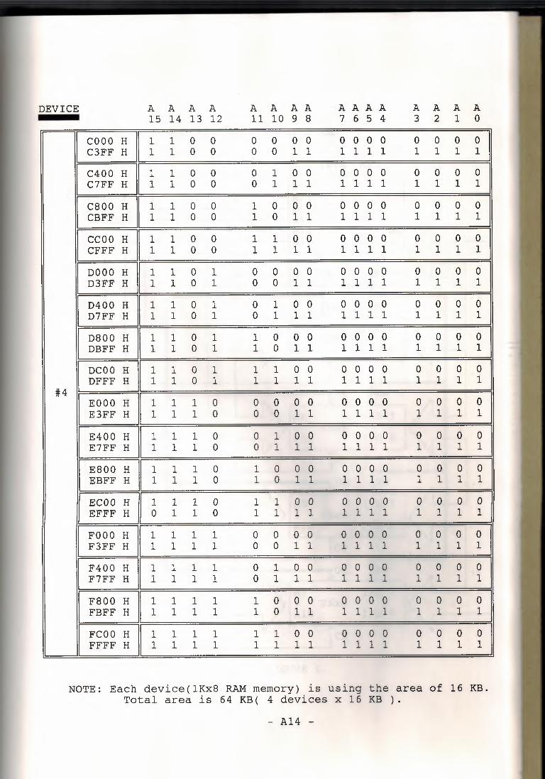
NOTE: Each device(1Kx8 RAM memory) is using the area of 16 KB. Total area is 64 KB( 4 devices x 16 KB).
- A14 -
INTERFACING WITH 2Kx8 RAM
6800 MPU
- Al5 2 to 4 - A14 LINE I - A13
DECODER I A12 All DO AlO . . . . . . . . .
: . . . AO RD WR D7 1
.. OE RW .
AO I/0 7 . 2Kx8 . . . . . AlO I/0 0
Tes .. JLOE RW .
< AO I/0 7 : 2Kx8 : : AlO I/0 0
Tes JLOE .II_RW ..
AO I/0 7 : 2Kx8 : . . AlO I/0 0
Tes JLOE RW ..
AO I/0 7 1< : 2Kx8 : : AlO I/0 0
Tes FIGURE 1.
- Al5 -
ADDRESS MAP FOR FIGURE 1
DEVICE A A A A A A A A A A A A A A A A
15 14 13 12 11 10 9 8 7 6 5 4 3 2 1 0
#1 II 0000 H I ~ 0 0 0 0 0 0 0 0 0 0 0 0 0 0 0
07FF H 0 0 0 0 1 1 1 1 1 1 1 1 1 1 1
#2 II 0800 H I g 0 0 0 1 0 0 0 0 0 0 0 0 0 0 0
OFFF H 0 0 0 1 1 1 1 1 1 1 1 1 1 1 1
#3 II 1000 H I g 0 0 1 0 0 0 0 0 0 0 0 0 0 0 0
17FF H 0 0 1 0 1 1 1 1 1 1 1 1 1 1 1
#4 11 1800 H \\ 0 0 0 1 1 0 0 0 0 0 0 0 0 0 0 0
lFFF H 0 0 0 1 1 1 1 1 1 1 1 1 1 1 1 1
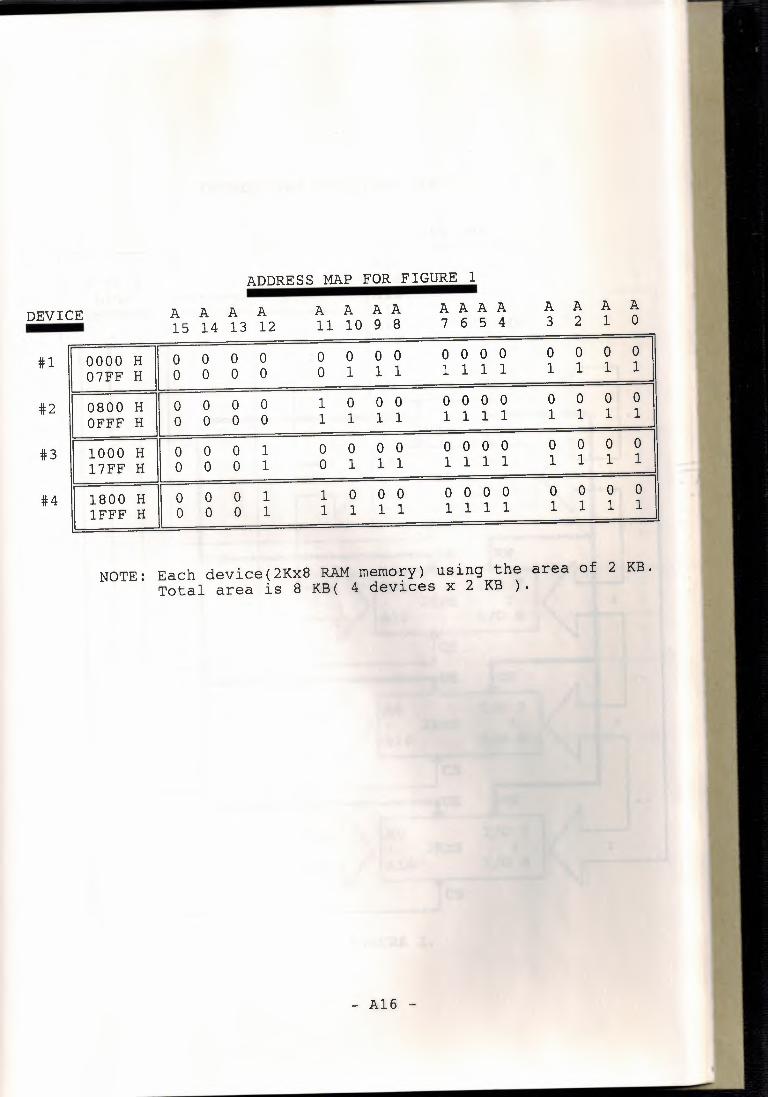
NOTE: Each device(2Kx8 RAM memory) using the area of 2 KB. Total area is 8 KB( 4 devices x 2 KB).
- Al6 -
INTERFACING WITH 2Kx8 RAM
6800 MPU
- Al5 2 to 4 - Al4 LINE Al3
DECODER Al2 - All DO
AlO . : . : . . . : : .
AO RD WR D7
.. OE RW J " ,.
AO I/0 7 : 2Kx8 . : . AlO I/0 0
Tes .. JLOE RW
AO I/0 7 : 2Kx8 . . . . AlO I/0 0
Tes JLOE lRW ..
AO I/0 7 : 2Kx8 . . . . AlO I/0 0
Tes JlOE JlRW ..
AO I/0 7 : 2Kx8 : . . AlO I/0 0
Tes FIGURE 2.
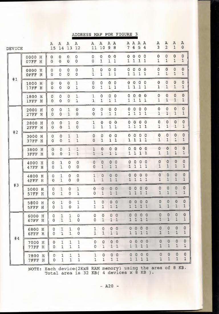
- Al7 -
ADDRESS MAP FOR FIGURE 2
DEVICE A A A A 15 14 13 12
A A A A 11 10 9 8
A A A A 7 6 5 4
A A A A 3 2 1 0
0000 H I g 0 0 0 0 0 0 0 0 0 0 0 0 0 0 ~ I 07FF H 0 0 0 0 1 1 1 1 1 1 1 1 1 1
#1 0800 H I g 0 0 0 1 0 0 0 0 0 0 0 0 0 0
~ I OFFF H 0 0 0 1 1 1 1 1 1 1 1 1 1 1
1000 H I g 0 0 1 0 0 0 0 0 0 0 0 0 0 0 ~ I 17FF H 0 0 1 0 1 1 1 1 1 1 1 1 1 1
#2 1800 H I g 0 0 1 1 0 0 0 0 0 0 0 0 0 0
~ I lFFF H 0 0 1 1 1 1 1 1 1 1 1 1 1 1
2000 H I g 0 1 0 0 0 0 0 0 0 0 0 0 0 0 ~ I 27FF H 0 1 0 0 1 1 1 1 1 1 1 1 1 1 #3
2800 H I g 0 1 0 1 0 0 0 0 0 0 0 0 0 0 ~ I 2FFF H 0 1 0 1 1 1 1 1 1 1 1 1 1 1
3000 H I ~ 0 1 1 0 0 0 0 0 0 0 0 0 0 0 ~ I 37FF H 0 1 1 0 1 1 1 1 1 1 1 1 1 1 #4
3800 H I g 0 1 1 1 0 0 0 0 0 0 0 0 0 0 ~ I 3FFF H 0 1 1 1 1 1 1 1 1 1 1 1 1 1
NOTE: Each device(2Kx8 RAM memory) is using the area of 4 KB. Total area is 16 KB( 4 devices x 4 KB).
- Al8 -

INTERFACING WITH 2Kx8 RAM
6800 MPU
- Al5 2 to 4 I Al4 LINE r Al3
DECODER - Al2 - All DO
AlO . : : : . . . : . .
AO RD WR D7
.. OE RW
' ' AO I/0 7 . 2Kx8 : : . AlO I/0 0
Tes .. Jl,OE RW
AO I/0 7 : 2Kx8 . . . . AlO I/0 0
Tes ]LOE RW ..
AO I/0 7 : 2Kx8 : . . AlO I/0 0
Tes JLOE RW ..
AO I/0 7 . 2Kx8 : : . AlO I/0 0
Tes FIGURE 3.
- Al9 -
-------
DEVICE
ADDRESS MAP FOR FIGURE 3
A A A A 15 14 13 12
A A A A 11 10 9 8
A A A A 7 6 5 4
A A A A 3 2 1 0
0000 H I ~
0 0 0 0 0 0 0 0 0 0 0 0 0 0 ~ I 07FF H 0 0 0 0 1 1 1 1 1 1 1 1 1 1
0800 H I ~
0 0 0 1 0 0 0 0 0 0 0 0 0 0 ~ I OFFF H 0 0 0 1 1 1 1 1 1 1 1 1 1 1
#1 1000 H
I ~
0 0 1 0 0 0 0 0 0 0 0 0 0 0 ~ I 17FF H 0 0 1 0 1 1 1 1 1 1 1 1 1 1
1800 H I ~
0 0 1 1 0 0 0 0 0 0 0 0 0 0 ~ I lFFF H 0 0 1 1 1 1 1 1 1 1 1 1 1 1
2000 H I ~
0 1 0 0 0 0 0 0 0 0 0 0 0 0 ~ I 27FF H 0 1 0 0 1 1 1 1 1 1 1 1 1 1
2800 H I ~ 0 1 0 1 0 0 0 0 0 0 0 0 0 0 ~ I 2FFF H 0 1 0 1 1 1 1 1 1 1 1 1 1 1
#2 3000 H
I ~
0 1 1 0 0 0 0 0 0 0 0 0 0 0 ~ I 37FF H 0 1 1 0 1 1 1 1 1 1 1 1 1 1
3800 H I ~
0 1 1 1 0 0 0 0 0 0 0 0 0 0 ~ I 3FFF H 0 1 1 1 1 1 1 1 1 1 1 1 1 1
4000 H I ~
1 0 0 0 0 0 0 0 0 0 0 0 0 0 ~ I 47FF H 1 0 0 0 1 1 1 1 1 1 1 1 1 1
4800 H I ~
1 0 0 1 0 0 0 0 0 0 0 0 0 0 ~ I 4FFF H 1 0 0 1 1 1 1 1 1 1 1 1 1 1
#3 5000 H
I ~
1 0 1 0 0 0 0 0 0 0 0 0 0 0 ~ I 57FF H 1 0 1 0 1 1 1 1 1 1 1 1 1 1
5800 H I ~
1 0 1 1 0 0 0 0 0 0 0 0 0 0 ~ I 5FFF H 1 0 1 1 1 1 1 1 1 1 1 1 1 1
6000 H I ~
1 1 0 0 0 0 0 0 0 0 0 0 0 0 ~ I 67FF H 1 1 0 0 1 1 1 1 1 1 1 1 1 1
6800 H I ~
1 1 0 1 0 0 0 0 0 0 0 0 0 0 ~ I 6FFF H 1 1 0 1 1 1 1 1 1 1 1 1 1 1
#4 7000 H
I 0 1 1 1 0 0 0 0 0 0 0 0 0 0 0
~ I 77FF H 0 1 1 1 0 1 1 1 1 1 1 1 1 1 1
7800 H I ~
1 1 1 1 0 0 0 0 0 0 0 0 0 0 ~ I 7FFF H 1 1 1 1 1 1 1 1 1 1 1 1 1 1
NOTE: Each device(2Kx8 RAM memory) using the area of 8 KB. Total area is 32 KB( 4 devices x 8 KB).
- A20 -
INTERFACING WITH 2Kx8 RAM
6800 MPU
A15
I 2 to 4 [ A14
LINE - A13 DECODER - A12
- All DO AlO .
: : : : : : .
AO RD WR D7
.. OE RW
'I,
AO I/0 7 : 2Kx8 : . . AlO I/0 0
Tes .. JLOE _\\_RW
AO I/0 7 : 2Kx8 . . . . AlO I/0 0
Tes JLOE RW ..
AO I/0 7 : 2Kx8 . : . AlO I/0 0
Tes ' lLOE RW ..
AO I/0 7 . 2Kx8 : : . AlO I/0 0
Tes
FIGURE 4.
- A21 -
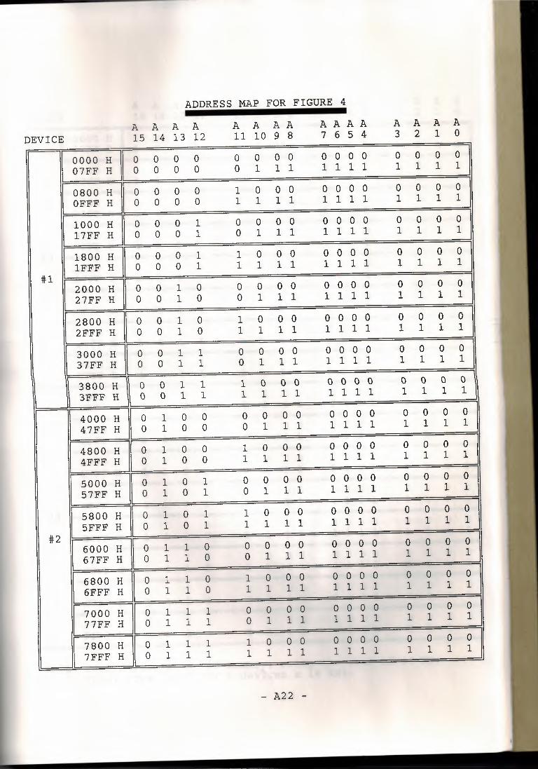
ADDRESS MAP FOR FIGURE 4
A A A A 3 2 1 0 DEVICE
A A A A 15 14 13 12
A A A A 11 10 9 8
A A A A 7 6 5 4
0000 H I g 0 0 0 0 0 0 0 0 0 0 0 0 0 0 ~ I 07FF H 0 0 0 0 1 1 1 1 1 1 1 1 1 1
0800 H I g 0 0 0 1 0 0 0 0 0 0 0 0 0 0 ~ I OFFF H 0 0 0 1 1 1 1 1 1 1 1 1 1 1
1000 H I g 0 0 1 0 0 0 0 0 0 0 0 0 0 0 ~ I 17FF H 0 0 1 0 1 1 1 1 1 1 1 1 1 1
1800 H I g 0 0 1 1 0 0 0 0 0 0 0 0 0 0
~ I lFFF H 0 0 1 1 1 1 1 1 1 1 1 1 1 1
#1 2000 H I g 0 1 0 0 0 0 0 0 0 0 0 0 0 0
~ I 27FF H 0 1 0 0 1 1 1 1 1 1 1 1 1 1
2800 H I g 0 1 0 1 0 0 0 0 0 0 0 0 0 0 ~ I 2FFF H 0 1 0 1 1 1 1 1 1 1 1 1 1 1
3000 H I g 0 1 1 0 0 0 0 0 0 0 0 0 0 0 ~ I 37FF H 0 1 1 0 1 1 1 1 1 1 1 1 1 1
3800 H ! 0 0 1 1 1 0 0 0 0 0 0 0 0 0 0 ~ l 0 1 1 1 1 1 1 1 1 1 1 1 1 1 3FFF H 0
4000 H I g 1 0 0 0 0 0 0 0 0 0 0 0 0 0
~ I 47FF H 1 0 0 0 1 1 1 1 1 1 1 1 1 1
4800 H I g 1 0 0 1 0 0 0 0 0 0 0 0 0 0
~ I 4FFF H 1 0 0 1 1 1 1 1 1 1 1 1 1 1
5000 H I g 1 0 1 0 0 0 0 0 0 0 0 0 0 0 ~ I 57FF H 1 0 1 0 1 1 1 1 1 1 1 1 1 1
5800 H I g 1 0 1 1 0 0 0 0 0 0 0 0 0 0 ~ I 5FFF H 1 0 1 1 1 1 1 1 1 1 1 1 1 1
#2
I g ~ I 6000 H 1 1 0 0 0 0 0 0 0 0 0 0 0 0
67FF H 1 1 0 0 1 1 1 1 1 1 1 1 1 1
6800 H I 0 1 1 0 1 0 0 0 0 0 0 0 0 0 0 ~ I 1 1 0 1 1 1 1 1 1 1 1 1 1 1
6FFF H 0
7000 H I g 1 1 1 0 0 0 0 0 0 0 0 0 0 0
~ I 77FF H 1 1 1 0 1 1 1 1 1 1 1 1 1 1
7800 H I g 1 1 1 1 0 0 0 0 0 0 0 0 0 0
~ I 7FFF H 1 1 1 1 1 1 1 1 1 1 1 1 1 1
- A22 -

uEVICE
A A A A 15 14 13 12
A A A A 11 10 9 8
A A A A 7 6 5 4
A A A A 3 2 1 0
8000 H I i 0 0 0 0 0 0 0 0 0 0 0 0 0 0 ~ I 87FF H 0 0 0 0 1 1 1 1 1 1 1 1 1 1
8800 H I i 0 0 0 1 0 0 0 0 0 0 0 0 0 0 ~ I 8FFF H 0 0 0 1 1 1 1 1 1 1 1 1 1 1
9000 H I t 0 0 1 0 0 0 0 0 0 0 0 0 0 0 ~ I
97FF H 0 0 1 0 1 1 1 1 1 1 1 1 1 1
9800 H I i 0 0 1 1 0 0 0 0 0 0 0 0 0 0 ~ I 9FFF H 0 0 1 1 1 1 1 1 1 1 1 1 1 1
#3 AOOO H I i 0 1 0 0 0 0 0 0 0 0 0 0 0 0 ~ I A7FF H 0 1 0 0 1 1 1 1 1 1 1 1 1 1
A800 H I t 0 1 0 1 0 0 0 0 0 0 0 0 0 0 ~ I AFFF H 0 1 0 1 1 1 1 1 1 1 1 1 1 1
BOOO H l i 0 1 1 0 0 0 0 0 0 0 0 0 0 0 ~ I B7FF H 0 1 1 0 1 1 1 1 1 1 1 1 1 1
B800 H I t 0 1 1 1 0 0 0 0 0 0 0 0 0 0 ~ I BFFF H 0 1 1 1 1 1 1 1 1 1 1 1 1 1
COOO H I t 1 0 0 0 0 0 0 0 0 0 0 0 0 0 ~ l
C7FF H 1 0 0 0 1 1 1 1 1 1 1 1 1 1
C800 H I t 1 0 0 1 0 0 0 0 0 0 0 0 0 0 ~ I CFFF H 1 0 0 1 1 1 1 1 1 1 1 1 1 1
DOOO H I t 1 0 1 0 0 0 0 0 0 0 0 0 0 0 ~ I D7FF H 1 0 1 0 1 1 1 1 1 1 1 1 1 1
D800 H I t 1 0 1 1 0 0 0 0 0 0 0 0 0 0 ~ I DFFF H 1 0 1 1 1 1 1 1 1 1 1 1 1 1
#4 EOOO H I t 1 1 0 0 0 0 0 0 0 0 0 0 0 0 ~ I E7FF H 1 1 0 0 1 1 1 1 1 1 1 1 1 1
E800 H I t 1 1 0 1 0 0 0 0 0 0 0 0 0 0 ~ I EFFF H 1 1 0 1 1 1 1 1 1 1 1 1 1 1
FOOO H I t 1 1 1 0 0 0 0 0 0 0 0 0 0 0 ~ I
F7FF H 1 1 1 0 1 1 1 1 1 1 1 1 1 1
F800 H I t 1 1 1 1 0 0 0 0 0 0 0 0 0 0 ~ I
FFFF H 1 1 1 1 1 1 1 1 1 1 1 1 1 1
NOTE: Each device(2Kx8 RAM memory) using the area of 16 KB, Total area is 64 KB( 4 devices x 16 KB).
- A23 -
.•••••.............. ~--~~~=-=-~
INTERFACING WITH 4Kx8 RAM
6800 MPU
2 to 4 LINE
DECODER
Al5 Al4
r\-------~1Al3
I Al2
r--------' All DO
....------1 AO RD WR D7
OE RW
AO I/0 7 4Kx8
All I/0 0
cs
AO I/0 7 4Kx8
All I/0 0 IT' cs
I RW -
AO I/0 7 4Kx8
All I/0 0
"' cs I RW . -
AO I/0 7 4Kx8
All I/0 0 ,,.,. cs
FIGURE 1.
- A24 -
DEVICE A A A A 15 14 13 12
A A A A 11 10 9 8
A A A A 7 6 5 4
A A A A 3 2 1 0
ADDRESS MAP FOR FIGURE 1
#1 0000 H 0 0 0 0 0 0 0 0 0 0 0 0 0 0 0 0 OFFF H 0 0 0 0 1 1 1 1 1 1 1 1 1 1 1 1
1000 H 0 0 0 1 0 0 0 0 0 0 0 0 0 0 0 0 lFFF H 0 0 0 1 1 1 1 1 1 1 1 1 1 1 1 1
2000 H 0 0 1 0 0 0 0 0 0 0 0 0 0 0 0 0 2FFF H 0 0 1 0 1 1 1 1 1 1 1 1 1 1 1 1
3000 H 0 0 1 1 0 0 0 0 0 0 0 0 0 0 0 0 3FFF H 0 0 1 1 1 1 1 1 1 1 1 1 1 1 1 1
#2
#3
#4
NOTE: Each device(4Kx8 RAM memory) is using the area of 4 KB. Total area is 16 KB( 4 devices x 4 KB).
- A25 -
- Al5 2 to 4 I Al4 LINE I Al3
DECODER - Al2 All DO
: : . : : . . . . : : .
AO RD WR D7
.. OE RW
'I, I,
AO I/0 7 : 4Kx8 . : . All I/0 0
Tes .. J~OE RW
AO I/0 7 : 4Kx8 : . . All I/0 0
fcs JLOE RW ..
AO I/0 7 : 4Kx8 . : . All I/0 0
Tes J~OE RW ..
AO I/0 7 : 4Kx8 . . . . All I/0 0
Tes
INTERFACING WITH 4Kx8 RAM
6800 MPU
FIGURE 2.
- A26 -
DEVICE A A A A 15 14 13 12
A A A A 11 10 9 8
A A A A 7 6 5 4
A A A A 3 2 1 0
ADDRESS MAP FOR FIGURE 2
0000 H I ~ 0 0 0 0 0 0 0 0 0 0 0 0 0 0 ~ I OFFF H 0 0 0 1 1 1 1 1 1 1 1 1 1 1 #1
1000 H I ~ 0 0 1 0 0 0 0 0 0 0 0 0 0 0 ~ I lFFF H 0 0 1 1 1 1 1 1 1 1 1 1 1 1
2000 H I ~ 0 1 0 0 0 0 0 0 0 0 0 0 0 0 ~ I 2FFF H 0 1 0 1 1 1 1 1 1 1 1 1 1 1
#2 3000 H I ~ 0 1 1 0 0 0 0 0 0 0 0 0 0 0
~ I 3FFF H 0 1 1 1 1 1 1 1 1 1 1 1 1 1
4000 H I ~ 1 0 0 0 0 0 0 0 0 0 0 0 0 0 ~ I 4FFF H 1 0 0 1 1 1 1 1 1 1 1 1 1 1
#3 5000 H
I ~
1 0 1 0 0 0 0 0 0 0 0 0 0 0 ~ I 5FFF H 1 0 1 1 1 1 1 1 1 1 1 1 1 1
6000 H I ~
1 1 0 0 0 0 0 0 0 0 0 0 0 0 ~ I 6FFF H 1 1 0 1 1 1 1 1 1 1 1 1 1 1
#4 7000 H I ~ 1 1 1 0 0 0 0 0 0 0 0 0 0 0
~ I 7FFF H 1 1 1 1 1 1 1 1 1 1 1 1 1 1
NOTE: Each device(4Kx8 RAM memory) using the area of 8 KB. Total area is 32 KB( 4 devices x 8 KB).
- A27 -
6800 MPU
INTERFACING WITH 4Kx8 RAM
- Al5 2 to 4 r Al4 LINE I Al3
DECODER - Al2 All DO
: : . : : : . . : : .
AO RD WR D7
.. OE RW
', 'II
AO I/0 7 : 4Kx8 : . . All I/0 0
Tes .. ,II.OE RW
AO I/0 7 : 4Kx8 . : . All I/0 0
Tes Jl,OE JRw ..
AO I/0 7 : 4Kx8 : . . All I/0 0
Tes J~OE JlRw ..
AO I/0 7 : 4Kx8 : . . All I/0 0
Tes FIGURE 3.
- A28 -

ADDRESS MAP FOR FIGURE 3
DEVICE
0000 H I ~ 0 0 0 0 0 0 0 0 0 0 0 0 0 0 ~ I OFFF H 0 0 0 1 1 1 1 1 1 1 1 1 1 1
1000 H I ~ 0 0 1 0 0 0 0 0 0 0 0 0 0 0 ~ I lFFF H 0 0 1 1 1 1 1 1 1 1 1 1 1 1
#1 2000 H I ~ 0 1 0 0 0 0 0 0 0 0 0 0 0 0 ~ I 2FFF H 0 1 0 1 1 1 1 1 1 1 1 1 1 1
3000 H I ~ 0 1 1 0 0 0 0 0 0 0 0 0 0 0 ~ I 3FFF H 0 1 1 1 1 1 1 1 1 1 1 1 1 1
4000 H I ~ 1 0 0 0 0 0 0 0 0 0 0 0 0 0 ~ I 4FFF H 1 0 0 1 1 1 1 1 1 1 1 1 1 1
5000 H I ~ 1 0 1 0 0 0 0 0 0 0 0 0 0 0 ~ I 5FFF H 1 0 1 1 1 1 1 1 1 1 1 1 1 1
#2 6000 H I ~ 1 1 0 0 0 0 0 0 0 0 0 0 0 0
~ I 6FFF H 1 1 0 1 1 1 1 1 1 1 1 1 1 1
7000 H I ~ 1 1 1 0 0 0 0 0 0 0 0 0 0 0 ~ I 7FFF H 1 1 1 1 1 1 1 1 1 1 1 1 1 1
8000 H I i 0 0 0 0 0 0 0 0 0 0 0 0 0 0 ~ I 8FFF H 0 0 0 1 1 1 1 1 1 1 1 1 1 1
9000 H I i 0 0 1 0 0 0 0 0 0 0 0 0 0 0 ~ I 9FFF H 0 0 1 1 1 1 1 1 1 1 1 1 1 1
#3 AOOO H
I
1 0 1 0 0 0 0 0 0 0 0 0 0 0 0 ~ I AFFF H 1 0 1 0 1 1 1 1 1 1 1 1 1 1 1
BOOO H I i 0 1 1 0 0 0 0 0 0 0 0 0 0 0 ~ I BFFF H 0 1 1 1 1 1 1 1 1 1 1 1 1 1
COOO H I t 1 0 0 0 0 0 0 0 0 0 0 0 0 0 ~ I CFFF H 1 0 0 1 1 1 1 1 1 1 1 1 1 1
DOOO H I t 1 0 1 0 0 0 0 0 0 0 0 0 0 0 ~ I DFFF H 1 0 1 1 1 1 1 1 1 1 1 1 1 1
#4 EOOO H
I
1 1 1 0 0 0 0 0 0 0 0 0 0 0 0 ~ I EFFF H 1 1 1 0 1 1 1 1 1 1 1 1 1 1 1
FOOO H I i 1 1 1 0 0 0 0 0 0 0 0 0 0 0 ~ I FFFF H 1 1 1 1 1 1 1 1 1 1 1 1 1 1
A A A A 15 14 13 12
A A A A 11 10 9 8
A A A A 7 6 5 4
A A A A 3 2 1 0
NOTE: Each device(4Kx8 RAM memory) is using the area of 16 KB. Total area is 64 KB( 4 devices x 16 KB).
- A29 -
•••••••••.••••.•..•......... ~~----==-~
INTERFACING WITH 16Kx8 RAM
6800 MPU
A15 2 to 4 LJ Al4 LINE I Al3
DECODER . : . : . DO . : : . . : . . . . . : . . .
AO RD WR D7
.. OE RW
'i, ' I
AO I/0 7 : 16Kx8 . . . . Al3 I/0 0
Tes .. Jl,OE RW
AO I/0 7 . 16Kx8 . . . . . Al3 I/0 0
Tes JI.OE J~w ..
AO I/0 7 : 16Kx8 . . . . A13 I/0 0
jcs .!LOE J[Rw ..
AO I/0 7 : 16Kx8 : . . A13 I/0 0
Tes FIGURE 1.
- A30 -

_. •••••••........... ----------~
ADDRESS MAP FOR FIGURE 1
DEVICE A A A A A A A A A A A A A A A A
15 14 13 12 11 10 9 8 7 6 5 4 3 2 1 0
#1 II 0000 H II 0 0 0 0 0 0 0 0 0 0 0 0 0 0 0 0
3FFF H 0 0 1 1 1 1 1 1 1 1 1 1 1 1 1 1
#2 II 4000 H II 0 1 0 0 0 0 0 0 0 0 0 0 0 0 0 0
7FFF H 0 1 1 1 1 1 1 1 1 1 1 1 1 1 1 1
#3 II 8000 H II 1 0 0 0 0 0 0 0 0 0 0 0 0 0 0 0
BFFF H 1 0 1 1 1 1 1 1 1 1 1 1 1 1 1 1
#4 II cooo H \I 1 1 0 0 0 0 0 0 0 0 0 0 0 0 0 0
FFFF H 1 1 1 1 1 1 1 1 1 1 1 1 1 1 1 1
NOTE: Each device(16Kx8 RAM memory) is using the area of 16 KB, Total area is 64 KB( 4 devices x 16 KB).
- A31 -
A P P E N D I X
~National ~ Semiconductor MM54HC32/MM74HC32 Quad z-tnput OR Gate General Description These OR gates utilize advanced silicon-gate CMOS tech nology to achieve operating speeds similar to LS-TIL gates with the low power consumption of standard CMOS inte grated circuits. All gates have buffered outputs, providing high noise immunity and the ability to drive 1 O LS-TIL loads. The 54HC/74HC logic family is functionally as well as pin out compatible with the standard 54LS/74LS logic family. All inputs are protected from damage due to static dis charge by internal diode clamps to Vee and ground.
Features • Typical propagation delay: 10 ns • Wide power supply range: 2-6V • Low quiescent current: 20 µA maximum (74HC Series) • Low input current: 1 µA maximum • Fanout of 10 LS-TIL loads
Connection and Logic Diagrams Dual-In-Line Package
Vee B4 A4 Y4 B3 A3 Y3
14 113 112 111 110 le la
2 3 4 5 6 7
GND A1 B1 Y1 A2 B2 Y2 TL/F/5132-1
Top View
Order Number MM54HC32• or MM74HC32' 'Please look into Section 8, Appendix D for availability of various package types
Y=A-B A
B
y
(1 of 4)
bsolute Maximum Ratings (Notes 1 & 2) Operating Conditions Mlllt~ry I Aerospace specified devices are required, Min Max Units ntact the National Semiconductor Sales Office/ Supply Voltage (Vee) 2 6 V 1trlbutors for availability and specifications. DC Input or Output Voltage 0 Vee V pply Voltage (Vee) -0.5 to+ 7.0V (V1N, vour) : Input Voltage (V1N) -1.5toVcc+1.5V Operating Temp. Range (T Al
: Output Voltage (Vour) -0.5 to Vee+ 0.5V MM74HC -40 + 85 'C
imp Diode Current (11K, ioK) t 20 mA MM54HC -55 +125 'C
: Output Current, per pin (lour) ±25 mA Input Rise or Fall Times
: Vee or GND Current, per pin (Ice) (tr, tt) Vcc=2.0V 1000 ns
±50 mA Vcc=4.5V 500 ns xage Temperature Range (T STG) - 65°C to + 150'C Vcc=6.0V 400 ns
wer Dissipation (Po) [Note 3) 600 mW S.0. Package only 500mW ad Temperature (TL) [Soldering 10 seconds) zso-c
C Electrical Characteristics (Note 4)
TA= zs-c 74HC 54HC
nbol Parameter Conditions Vee TA= -40 to 65'C TA= -55 to 125°C Units
Typ Guaranteed Limits
Minimum High Level 2.0V 1.5 1.5 1.5 V Input Voltage 4.5V 3.15 3.15 3.15 V
6.0V 4.2 4.2 4.2 V
Maximum Low Level 2.0V 0.5 0.5 0.5 V
Input Voltage •• 4.5V 1.35 1.35 1.35 V 6.0V 1.8 1.8 1.8 V
H Minimum High Level V1N = V1H or V1L Output Voltage liourls:20 µA 2.0V 2.0 1.9 1.9 1.9 V
4.5V 4.5 4.4 4.4 4.4 V 6.0V 6.0 5.9 5.9 5.9 V
V1N = V1H or V1L llourl ~4.0 mA 4.5V 4.7 3.98 3.84 3.7 V
l1ourl~5.2 mA 6.0V 5.2 5.48 5.34 5.2 V
L Maximum Low Level V1N=V1L Output Voltage I 'ourl ~ 20 µA 2.0V 0 0.1 0.1 0.1 V
4.5V 0 0.1 0.1 0.1 V 6.0V 0 0.1 0.1 0.1 V
V1N=V1L l1ourl~4.0mA 4.5V 0.2 0.26 0.33 0.4 V
l'ourl ~ 5.2 mA 6.0V 0.2 0.26 0.33 0.4 V
Maximum Input V1N=VccorGND 6.0V ±0.1 I1.0 = 1.0 µA
Current
; Maximum Quiescent V1N = Vee or GND 6.0V 2.0 20 40 µA
Supply Current lour=O µA ote 1: Absolute Maximum Ratings are those values beyond which damage 10 the device may occur.
ote 2: Un!ess otherwise specified all voltages are referenced to ground. ote 3: Power Dissipation temperature derating - plastic "N" package: -12 mW/"C from 65"C 10 BS'C; ceramic "J" pacxaqe -12 rn',', ·c from 1ocrC 10 12s·c.
ote 4: For a power supply of SV ± 10% the worst case output voltages (VoH, and VOLi occur for HC at 4.SV_ Thus 1he <_SV .a Jes snoulo be used when >signing with this supply. Worst case v1H and v1L occur al Vee= 5.SV and 4.5V respectivelv. (The V1H value at 5.SV rs 3 85V -ne .,,o,s: case eaxaqs current Cl1N, C, and 1oz) occur for CMOS al the higher voltage and so the 6.0V values should be used V1L limits are currently tested al 20% of Vee- The above V1L specification (30% of Vee) will be ,mplemen1ed no later than 01 cv·sg_

_ ••••........ _. ••....... ----------~~ Electrical Characteristics vo:,=5V, TA=25°C. CL= 15 pF, t,=tr=6 ns
ymbol Parameter Conditions Typ Guaranteed I Units
Limit
~L, lpl_H Maximum Propagation 10 18 I ns
Delay --·- I I -· I
: Electrical Characteristics I
= 2.0V to 6.0V. CL= 50 pF, t, =tr= 6 ns (unless otherwise specified) - TA=25°C
74HC 54HC
ibol Parameter Conditions Vee TA= - 40 to 85°C TA= - 55 to 125°C Units
Typ Guaranteed Limits - \pLH Maximum Propagation 2.0V 30 100 125 150 ns
Delay 4.5V 12 20 25 30 ns
6.0V 9 17 21 25 ns -
, tTHL Maximum Output Rise 2.0V 30 75 95 110 ns
and Fall Time 4.5V 8 15 19 22 ns
6.0V 7 13 16 19 ns
Power Dissipation (per gate) 50 pF '·
Capacitance (Note 5)
Maximum Input 5 10 10 10 pF
Capacitance ,e 5: Cpo detennines the no load dynamic power consurnptioo, Po= Cpo V cc2 f + Ice V cc, and the no load dynamic current consumption, Is= Cpo V cc f + Ice.
Connection and Logic Diagrams
Features • Typical propagation delay: 8 ns • Fan out of 10 LS-TIL loads • Quiescent power consumption: 10 JJ-W maximum at
room temperature • Low input current: 1 µA maximum
~National D Semiconductor MM54HC04/MM74HC04 Hex Inverter General Description These inverters utilize advanced silicon-gate CMOS tech nology to achieve operating speeds similar to LS-TIL gates with the low power consumption of· standard CMOS inte grated circuits. The MM54HC04/MM74HC04 is a triple buffered inverter. It has high noise immunity and the ability to drive 10 LS-TIL loads. The 54HC/7 4HC logic family is functionally as well as pin-out compatible with the standard 54LSl74LS logic fami ly. All inputs are protected from damage due to static dis charge by internal diode clamps to Vee and ground.
Dual-In-Line Package
vee A6 Y6 AS Y5 A4 Y4
14 13 12 11 10 9
4 5 7
A1 Y1 A2 Y2 AJ YJ GND TL/F/5069-1
Top View
Order Number MM54HC04' or MM74HC04 • 'Please look into Section 8, Appendix D for availability of vanous pacsaqe iypes
1 of 6 Inverters
"L F, 50€9-2

put Voltage (VouTl
Diode Current (l1K, ioKl
iput Current, per pin (louTl
~ or GND Current, per pin (Ice)
e Temperature Range (T STG)
Dissipation (Po) e 3) Package only ·emperature (T Ll daring 1 O seconds)
-0.5toVce+05V ±20 mA ±25 mA ±50 mA
- 65'C to + 150'C
~
Operating Conditions ~ c.n .i:,.
Min Max Units :c Supply Voltage (Vee) 2 6 V ()
0
DC Input or Output Voltage 0 Vee V .i:,. ...._
(VIN, Vou1) ~ ~
Operating Temp. Range (T Al -..J
MM74HC -40 t 85 'C .i:,. :c
MM54HC -55 + 125 'C () 0
Input Rise or Fall Times .i:,.
(tr, It) Vee=20V 1000 ns
Vee= 4 5V 500 ns
Vee= s.ov 400 ns
rlute Maximum Ratings (Notes 1 & 2) ary I Aerospace specified devices are required, t the National Semiconductor Sales Office/ utors for availability and specifications. Voltage (Vee) -0.5 to + 7.0V Jt Voltage (ViN) -1.5 to Vee+ 1.5V
600mW 500 mW
260'C
Electrical Characteristics (Note 4)
TA =2S'C 74HC 54HC
I Parameter Conditions Vee TA= - 40 to 8S'C TA=-55to125'C Units
Typ Guaranteed Limits
Minimum High Level 2.0V 1.5 1.5 1.5 V
Input Voltage 4.5V 3.15 3.15 3.15 V
6.0V 4.2 4.2 4.2 V
Maximum Low Level 2.0V 0.5 0.5 0.5 V
Input Voltage•• 4.5V 1.35 1.35 1.35 V
6.0V 1.8 1.8 1.8 V
Minimum High Level V1N = V1L Output Voltage I lour Is 20 µA 2.0V 2.0 1.9 1.9 1.9 V
4.5V 4.5 4.4 4.4 4.4 V
6.0V 6.0 5.9 5.9 5.9 V
V1N=V1L l1ourls4.0 mA 4.5V 4.2 3.98 3.84 3.7 V
liouTI s 5.2 mA 6.0V 5.7 5.48 5.34 5.2 V
Maximum Low Level V1N=V1H Output Voltage I 'curl s 20 µA 2.0V 0 0.1 0.1 0.1 V
4.5V 0 0.1 0.1 0.1 V
6.0V 0 0.1 0.1 0.1 V
V1N=V1H l1ouTls4.0 mA 4.5V 0.2 0.26 0.33 0.4 V
l1ouTls5.2 mA 6.0V 0.2 0.26 0.33 0.4 V
Maximum Input V1N = Vee or GND 6.0V ±0.1 = 1.0 I ± 1.0 µA
Current
Maximum Quiescent V1N=VeeorGND 6.0V 2.0 20 I 40 µA
Supply Current louT=O µA 1: Absolute Maximum Ratings are those values beyond which damage to the device may occur.
2: Unless otherwise specified all voltages are referenced to ground. 3: Power Dissipation temperature dera1,ng - plastic "N" package: -12 mWl"C horn 65"C to 85"C; cerarn-c J. pacxace •2 mt, -~c from 100°C to t 25"C.
4: For a power supply of SY ± 10% t11e worst case output voltages (YoH, and Vey.) occur for HG at 4.SV. Tnus me< 5\ ,,, es s'lQUld oe used when designing this supply. Worst case v,H and v1L occur at Vee= 5.5V and 4.SV respectively. (1 he V1H value at 5.5V rs 3 85V Tile nor' case ea,age current (l1N, Ice. and
occur for CMOS at the higher voltage ano so the 6.0Y values should be used. limits are currently tested at 20% or Vee, The above v1L specification (30%, of Vee) will bo implemented no atee Ulan 01 cv·sg
•••••.......... ----------_...........-,=~·
lectrical Characteristics Vee= 5V, TA =25°c. cL = 15 pF. tr= ti =6 ns
)01 Parameter Conditions Typ Guaranteed Units
Limit
PLH Maximum Propagation 8 15 ns
Delay
.lectrlcal Characteristics Vee= 2.0V to 6.0V, CL= 50 pF, tr= ti= 6 ns (unless otherwise specified)
I TA=25'C 74HC 54HC
I I Parameter \ Conditions \ Vee TA= -40 to 85'C TA= - 55 to 125'C I Units I Typ Guaranteed Limits
H I Maximum Propagation I I 2.0V 55 95 120 145 ns
Delay 4.5V 11 19 24 29 ns
6.0V 9 16 20 24 ns
IL I Maximum Output Rise I I 2.0V 30 75 95 110 ns
and Fall Time 4.5V 8 15 19 22 ns
6.0V 7 13 16 19 ns
Power Dissipation I (per gate) I 20 pF
Capacitance (Note 5) I Maximum Input I I 5 I 10 I 10 I 10 I pF
Capacitance I I I
Cpo determines the no load dynamic power consumption. Po= Cpo Vo::;1 f + Ice Vee, and the no load dynamic current consumption, Is= Cpo Vee f + Ice.
~National ~· Semiconductor IM54HC 138/MM7 4HC 138 -to-8 Line Decoder 1eneral Description iis decoder utilizes advanced silicon-gate CMOS technol !Y, and is well suited to memory address decoding or data uting applications. The circuit features high noise immuni- and low power consumption usually associated with
MOS circuitry, yet has speeds comparable to low power
chottky TTL logic. he MM54HC138/ MM7 4HC138 has 3 binary select inputs ~. B, and C). If the device is enabled these inputs deter iine which one of the eight normally high outputs will go )W. Two active low and one active high enables (G1, G2A ind G2B) are provided to ease the cascading of decoders.
The decoder's outputs can drive 10 low power Schottky TTL equivalent loads, and are functionally and pin equivalent to the 54LS 138/7 4LS 138. All inputs are protected from dam age due to static discharge by diodes to Vee and ground.
Features • Typical propagation delay: 20 ns • Wide power supply range: 2V-6V • Low quiescent current: 80 µA maximum (7 4HC Series)
• Low input current: 1 µA maximum • Fanout of 1 O LS-TTL loads
:onnection and Logic Diagrams 15
o--YO Dual-In-Line Package
DATA OUTPUTS
Vee YO Y1 Y2 Y3 Y4 Y5 Y6 I I I r l ...+--i JV"r-vt \....--I '>a-- Y1
16 \1s \14 \13 \12 In \10
A
m5 m m 01 YT ONO m
OUTPUT SELECT ENABLE
TOP VIEW TL/F/5120-1
Order Number MM54HC138* or MM74HC138* 6 --L.r G1
'Please look into Section 8, Appendix D for
TL/F/5120-2
availability of various package types.
Truth Table Inputs I Outputs
Enable Select
G1 G2* C B A YO Y1 Y2 Y3 Y4 YS YG V7
X H X X X H H H H H H H H
L X X X X H H H H H H H H
H L L L L L H H H H H H H
H L L L H H L H H H H H H
H L L H L H H L H H H H H
H L L H H H H H L H H H H
H L H L L H H H H L H H H
H L H L H H H H H H L H H
H L H H L H H H H H H L H
H L H H H H H H H H H H L
'G2= G2A+ G2B H = high level, L = low level, X = don't care
3-108

3:
bsolute Maximum Ratings (Notes 1 & 2) Operating Conditions
3: 0,
Military I Aerospace specified devices are required, Min Max Units
.a;:.. ::c
ntact the National Semiconductor Sales Office/ Supply Voltage (Vee) 2 6 V 0
stributors for availability and specifications.
...• DC Input or Output Voltage 0 Vee V c.)
1pply Voltage (Vee) -0.5 to + 7.0V MN, vour)
(X) - ~ Input Voltage (V1Nl
-1.5toVee+1.5V Operating Temp. Range (T Al 3:: s:
::: Output Voltage (Vour) -0.5 to Vee+ o.5V
MM74HC -40 +85 oc ......•
MM54HC -55 + 125 oc .a;:..
amp Diode Current (l1K, loKl ±20 mA
::c
C Output Current, per pin (lour) ±25 mA
Input Rise or Fall Times 0
(tr, t1) Vee=2.0V 1000 ...•
ns c.)
C Vee or GND Current, per pin (lee) ±50 mA Vee= 4.5V 500 ns QO
torage Temperature Range (T src) -65°C to + 150°c Vee=6.0V 400 ns
ower Dissipation (Po) (Note3)
600mW
S.O. Package only 500mW
.ead Temp. (T Ll (Soldering 10 seconds) 260°C
~C Electrical Characteristics (Note 4l TA=25°C
74HC 54HC
vmbol Parameter Conditions Vee TA= -40to85°C TA= - 55 to 125°C Units
Typ Guaranteed Limits
IH Minimum High Level 2.0V 1.5 1.5 1.5 V
. Input Voltage 4.5V 3.15 3.15 3.15 V
6.0V 4.2 4.2 4.2 V
'IL Maximum Low Level 2.0V 0.5 0.5 0.5 V
Input Voltage•• 4.5V 1.35 1.35 1.35 V
6.0V 1.8 1.8 1.8 V
loH Minimum High Level V1N = V1H or V1L
Output Voltage \lourlQO µA 2.0V 2.0 1.9 1.9 1.9 V
4.5V 4.5 4.4 4.4 4.4 V
6.0V 60 5.9 5.9 5.9 V
V1N=V1HorV1L \lourls4.0 mA 4.5V 4.2 3.98 3.84 3.7 V
l1ourls5.2 mA 6.0V 5.7 5.48 5.34 5.2 V
VoL Maximum Low Level V1N = V1H or V1L
Output Voltage I lour I s 20 µA 2.0V 0 0.1 0.1 0.1 V
4.5V 0 0.1 0.1 0.1 V
6.0V 0 0.1 0.1 0.1 V
V1N = V1H or V1L \lourl s4.0 mA 4.5V 0.2 0.26 0.33 0.4 V
l1ourls5.2mA 6.0V 0.2 0.26 0.33 0.4 V
l1N Maximum Input V1N=Vee or GND 6.0V ±0.1 ±1.0 ± 1.0 µA
Current
Ice Maximum Quiescent V1N=VccorGND 6.0V 8.0 80 160 µA
Supply Current lour=O µA Note 1: Absolute Maximum Ratings are those values beyond which damage to the device may occur.
1
Note 2: Unless otherwise specified all voltages are referenced to ground.
i
Note 3: Power Dissipation temperature derating - plastic "N" package: -12 mW /'C from 65°C to 85°C; ceramic "J" package: -12 mW /'C from 100°C to 125°C. Note 4: For a power supply of 5V ± 10% the worst case output voltages (VoH, and Voll occur for HC at 4.5V. Thus the 4.5V values should be used when designing with this supply. Worst case ViH and Vil occur at Vee= 5.5V and 4.5V respectively. (The V1H value at 5.5V is 3.85V.) The worst case leakage current (l1N, Ice, and 1oz) occur for CMOS at the higher voltage and so the 6.0V values should be used. "Vil limits are currently tested at 20% of Vee, The above Vil specification (30% of Vccl will be implemented no later than 01, CY'89.
' 3-109
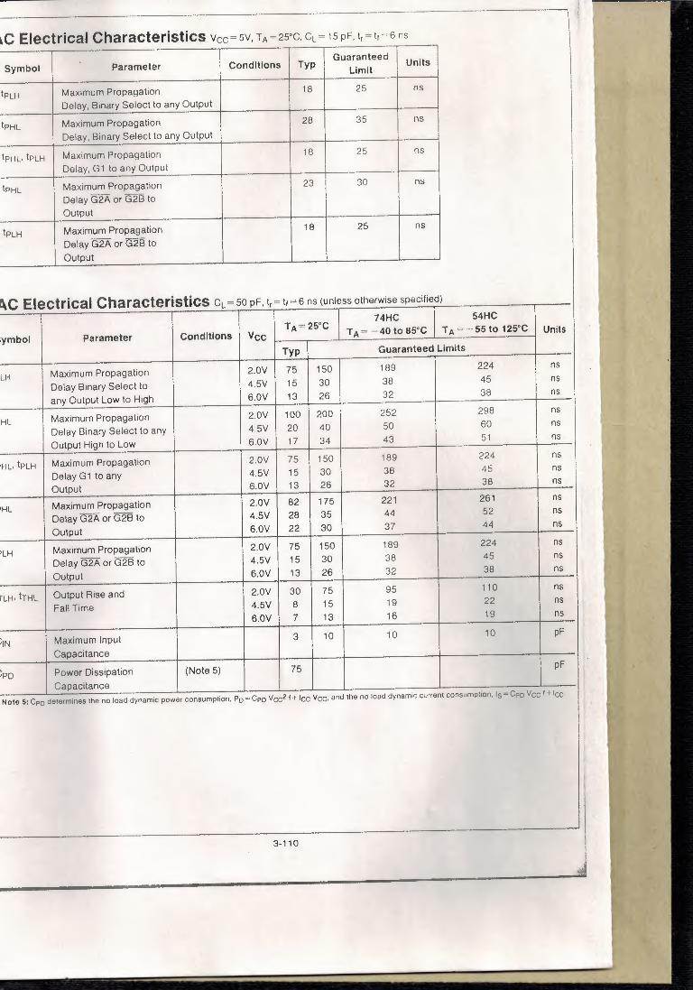
,l 1
~c Electrical Characteristics Vcc=5V, TA=25°C, CL= 15 pF, tr=t1=6 ns Symbol Parameter Conditions Typ
Guaranteed Units Limit
tPLH Maximum Propagation 18 25 ns
Delay, Binary Select to any Output
tpHL Maximum Propagation 28 35 ns
Delay, Binary Select to any Output
tpHL, tpLH Maximum Propagation 18 25 ns
Delay, G1 to any Output
tPHL Maximum Propagation 23 30 ns
Delay G2A or G2B to Output
tpLH Maximum Propagation 18 25 ns
Delay G2A or G2B to Output
~c Electrical Characteristics CL =50 pF, tr=t1=6 ns (unless otherwise specified) TA=25°C
74HC 54HC
,ymbol Parameter Conditions Vee TA= - 40 to 85°C TA=-55to125°C Units
Typ Guaranteed Limits
LH Maximum Propagation 2.0V 75 150 189 224 ns
Delay Binary Select to 4.5V 15 30 38 45 ns
any Output Low to High 6.0V 13 26 32 38 ns
HL Maximum Propagation 2.0V 100 200 252 298 ns
Delay Binary Select to any 4.5V 20 40 50 60 ns
Output High to Low 6.0V 17 34 43 51 ns
'HL, tpLH Maximum Propagation 2.0V 75 150 189 224 ns
Delay G 1 to any 4.5V 15 30 38 45 ns
Output 6.0V 13 26 32 38 ns
'HL Maximum Propagation 2.0V 82 175 221 261 ns ' Delay G2A or G2B to 4.5V 28 35 44 52 ns I
Output 6.0V 22 30 37 44 ns
'LH Maximum Propagation 2.0V 75 150 189 224 ns
Delay G2A or G2B to 4.5V 15 30 38 45 ns
Output 6.0V 13 26 32 38 ns
rLH, trnL Output Rise and 2.0V 30 75 95 110 ns
Fall Time 4.5V 8 15 19 22 ns
6.0V 7 13 16 19 ns
;IN Maximum Input 3 10 10 10 pF
Capacitance
:po Power Dissipation (Note 5) 75 pF
Capacitance Note 5: Cpo determines the no load dynamic power consumption, Po= Cpo Vcc2 f + Ice Vee, and the no load dynamic current consumption. Is= Cpo Vee f + Ice-
3-110