mx25l3235e - rs components · - the software protected mode (spm) uses (bp3, bp2, bp1, bp0) bits to...
TRANSCRIPT
1
MX25L3235E
P/N: PM1773 REV. 1.6, JUN. 27, 2014
MX25L3235E
HIGH PERFORMANCE
SERIAL FLASH SPECIFICATION
2
MX25L3235E
P/N: PM1773 REV. 1.6, JUN. 27, 2014
Contents
1. FEATURES ........................................................................................................................................................ 42. GENERAL DESCRIPTION ............................................................................................................................... 6
Table 1. Read Performance ..................................................................................................................63. PIN CONFIGURATION ...................................................................................................................................... 74. PIN DESCRIPTION ............................................................................................................................................ 75. BLOCK DIAGRAM ............................................................................................................................................. 86. DATA PROTECTION .......................................................................................................................................... 9
Table 2. Protected Area Sizes ..............................................................................................................10Table 3. 4K-bit Secured OTP Definition ............................................................................................... 11
7. MEMORY ORGANIZATION ............................................................................................................................. 12Table 4. Memory Organization .............................................................................................................12
8. DEVICE OPERATION ...................................................................................................................................... 139. HOLD FEATURE .............................................................................................................................................. 1410. COMMAND DESCRIPTION ........................................................................................................................... 15
Table 5. Command Sets .......................................................................................................................1510-1. Write Enable (WREN) ..........................................................................................................................1810-2. Write Disable (WRDI) ...........................................................................................................................1910-3. Read Identification (RDID) ...................................................................................................................2010-4. Read Status Register (RDSR) .............................................................................................................2110-5. Write Status Register (WRSR) .............................................................................................................24
Table 6. Protection Modes ....................................................................................................................2510-6. Read Data Bytes (READ) ....................................................................................................................2710-7. Read Data Bytes at Higher Speed (FAST_READ) ..............................................................................2810-8. Dual Read Mode (DREAD) ..................................................................................................................2910-9. 2 x I/O Read Mode (2READ) ...............................................................................................................3010-10. Quad Read Mode (QREAD) ................................................................................................................3110-11. 4 x I/O Read Mode (4READ) ...............................................................................................................3210-12. Performance Enhance Mode ...............................................................................................................3310-13. Performance Enhance Mode Reset (FFh) ...........................................................................................3310-14. Sector Erase (SE) ................................................................................................................................3610-15. Block Erase (BE) .................................................................................................................................3710-16. Block Erase (BE32K) ...........................................................................................................................3810-17. Chip Erase (CE) ...................................................................................................................................3910-18. Page Program (PP) .............................................................................................................................4010-19. 4 x I/O Page Program (4PP) ................................................................................................................4110-20. Continuous Program mode (CP mode) ................................................................................................4410-21. Deep Power-down (DP) .......................................................................................................................4610-22. Release from Deep Power-down (RDP), Read Electronic Signature (RES) .......................................4710-23. Read Electronic Manufacturer ID & Device ID (REMS), (REMS2), (REMS4) .....................................4910-24. ID Read ................................................................................................................................................50
Table 7. ID Definitions .........................................................................................................................5010-25. Enter Secured OTP (ENSO) ................................................................................................................5010-26. Exit Secured OTP (EXSO) ...................................................................................................................5010-27. Read Security Register (RDSCUR) .....................................................................................................51
Table 8. Security Register Definition ....................................................................................................52
3
MX25L3235E
P/N: PM1773 REV. 1.6, JUN. 27, 2014
10-28. Write Security Register (WRSCUR) .....................................................................................................5310-29. Write Protection Selection (WPSEL) ....................................................................................................5310-30. Single Block Lock/Unlock Protection (SBLK/SBULK) ..........................................................................5710-31. Read Block Lock Status (RDBLOCK) ..................................................................................................6010-32. Gang Block Lock/Unlock (GBLK/GBULK) ...........................................................................................6110-33. Enable SO to Output RY/BY# (ESRY) .................................................................................................6210-34. Disable SO to Output RY/BY# (DSRY) ................................................................................................6210-35. No Operation (NOP) ............................................................................................................................6210-36. Software Reset (Reset-Enable (RSTEN) and Reset (RST)) ...............................................................6210-37. Read SFDP Mode (RDSFDP) ..............................................................................................................63
Table 9. Signature and Parameter Identification Data Values .............................................................64Table 10. Parameter Table (0): JEDEC Flash Parameter Tables .........................................................65Table 11. Parameter Table (1): Macronix Flash Parameter Tables .......................................................67
11. POWER-ON STATE ....................................................................................................................................... 6912. ELECTRICAL SPECIFICATIONS .................................................................................................................. 70
12-1. Absolute Maximum Ratings .................................................................................................................7012-2. Capacitance .........................................................................................................................................70
Table 12. DC Characteristics ................................................................................................................72Table 13. AC Characteristics ................................................................................................................73
13. TIMING ANALYSIS ........................................................................................................................................ 75Table 14. Power-Up Timing .................................................................................................................77
13-1. Initial Delivery State .............................................................................................................................7714. OPERATING CONDITIONS ........................................................................................................................... 7815. ERASE AND PROGRAMMING PERFORMANCE ........................................................................................ 8016. DATA RETENTION ........................................................................................................................................ 8017. LATCH-UP CHARACTERISTICS .................................................................................................................. 8018. ORDERING INFORMATION .......................................................................................................................... 8119. PART NAME DESCRIPTION ......................................................................................................................... 8220. PACKAGE INFORMATION ............................................................................................................................ 8321. REVISION HISTORY ..................................................................................................................................... 86

4
MX25L3235E
P/N: PM1773 REV. 1.6, JUN. 27, 2014
32M-BIT [x 1/x 2/x 4] CMOS MXSMIO® (SERIAL MULTI I/O) FLASH MEMORY
1. FEATURES
GENERAL• Supports Serial Peripheral Interface -- Mode 0 and Mode 3• 33,554,432 x 1 bit structure or 16,777,216 x 2 bits (two I/O mode) structure or 8,388,608 x 4 bits (four I/O
mode) structure• 1024 Equal Sectors with 4K bytes each - Any Sector can be erased individually• 128 Equal Blocks with 32K bytes each - Any Block can be erased individually• 64 Equal Blocks with 64K bytes each - Any Block can be erased individually• Power Supply Operation - 2.7 to 3.6 volt for read, erase, and program operations• Latch-up protected to 100mA from -1V to Vcc +1V
PERFORMANCE• High Performance VCC = 2.7~3.6V - Normal read - 50MHz - Fast read - 1 I/O: 104MHz with 8 dummy cycles - 2 I/O: 86MHz with 4 dummy cycles for 2READ instruction - 4 I/O: Up to 104MHz - Configurable dummy cycle number for 4 I/O read operation - Fast program time: 0.7ms(typ.) and 3ms(max.)/page (256-byte per page) - Byte program time: 12us (typical) - Continuous Program mode (automatically increase address under word program mode) - Fast erase time: 30ms (typ.)/sector (4K-byte per sector) ; 0.25s(typ.) /block (64K-byte per block); 10s(typ.) /
chip • Low Power Consumption - Low active read current: 19mA(max.) at 104MHz, 10mA(max.) at 33MHz - Low active programming current: 15mA (typ.) - Low active sector erase current: 10mA (typ.) - Low standby current: 15uA (typ.) - Deep power down current: 1uA (typ.) • Typical 100,000 erase/program cycles• 20 years data retention
5
MX25L3235E
P/N: PM1773 REV. 1.6, JUN. 27, 2014
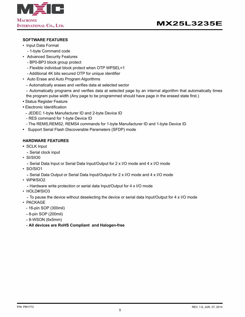
SOFTWARE FEATURES• Input Data Format - 1-byte Command code• Advanced Security Features - BP0-BP3 block group protect - Flexible individual block protect when OTP WPSEL=1 - Additional 4K bits secured OTP for unique identifier• Auto Erase and Auto Program Algorithms - Automatically erases and verifies data at selected sector - Automatically programs and verifies data at selected page by an internal algorithm that automatically times
the program pulse width (Any page to be programmed should have page in the erased state first.)• Status Register Feature• Electronic Identification - JEDEC 1-byte Manufacturer ID and 2-byte Device ID - RES command for 1-byte Device ID - The REMS,REMS2, REMS4 commands for 1-byte Manufacturer ID and 1-byte Device ID• Support Serial Flash Discoverable Parameters (SFDP) mode
HARDWARE FEATURES• SCLK Input - Serial clock input• SI/SIO0 - Serial Data Input or Serial Data Input/Output for 2 x I/O mode and 4 x I/O mode• SO/SIO1 - Serial Data Output or Serial Data Input/Output for 2 x I/O mode and 4 x I/O mode • WP#/SIO2 - Hardware write protection or serial data Input/Output for 4 x I/O mode• HOLD#/SIO3 - To pause the device without deselecting the device or serial data Input/Output for 4 x I/O mode• PACKAGE - 16-pin SOP (300mil) - 8-pin SOP (200mil) - 8-WSON (6x5mm) - All devices are RoHS Compliant and Halogen-free
6
MX25L3235E
P/N: PM1773 REV. 1.6, JUN. 27, 2014
2. GENERAL DESCRIPTION
MX25L3235E is 32Mb bits serial Flash memory, which is configured as 4,194,304 x 8 internally. When it is in two or four I/O mode, the structure becomes 16,777,216 bits x 2 or 8,388,608 bits x 4. MX25L3235E feature a se-rial peripheral interface and software protocol allowing operation on a simple 3-wire bus while it is in single I/O mode. The three bus signals are a clock input (SCLK), a serial data input (SI), and a serial data output (SO). Se-rial access to the device is enabled by CS# input.
MX25L3235E, MXSMIO® (Serial Multi I/O) flash memory, provides sequential read operation on whole chip and multi-I/O features.
When it is in dual I/O mode, the SI pin and SO pin become SIO0 pin and SIO1 pin for address/dummy bits input and data output. When it is in quad I/O mode, the SI pin, SO pin, WP# pin and HOLD# pin become SIO0 pin, SIO1 pin, SIO2 pin and SIO3 pin for address/dummy bits input and data Input/Output.
After program/erase command is issued, auto program/ erase algorithms which program/ erase and verify the specified page or sector/block locations will be executed. Program command is executed on byte basis, or page (256 bytes) basis, or word basis for Continuous Program mode, and erase command is executed on sector (4K-byte), block (32K-byte/64K-byte), or whole chip basis.
To provide user with ease of interface, a status register is included to indicate the status of the chip. The status read command can be issued to detect completion status of a program or erase operation via WIP bit.
When the device is not in operation and CS# is high, it is put in standby mode.
The MX25L3235E utilizes Macronix's proprietary memory cell, which reliably stores memory contents even after 100,000 program and erase cycles.
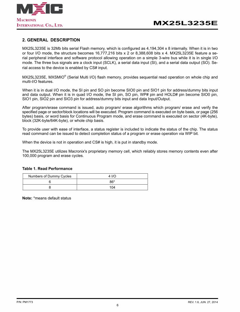
Table 1. Read Performance
Numbers of Dummy Cycles 4 I/O6 86*8 104
Note: *means default status

7
MX25L3235E
P/N: PM1773 REV. 1.6, JUN. 27, 2014
3. PIN CONFIGURATION
8-WSON (6x5mm)
1234
CS#SO/SIO1
WP#/SIO2GND
8765
VCCHOLD#/SIO3SCLKSI/SIO0
4. PIN DESCRIPTIONSYMBOL DESCRIPTION
CS# Chip Select
SI/SIO0Serial Data Input (for 1xI/O)/ Serial Data Input & Output (for 2xI/O or 4xI/O mode)
SO/SIO1Serial Data Output (for 1xI/O)/Serial Data Input & Output (for 2xI/O or 4xI/O mode)
SCLK Clock Input
WP#/SIO2Write protection: connect to GND or Serial Data Input & Output (for 4xI/O mode)
HOLD#/SIO3
To pause the device without deselecting the device or Serial data Input/Output for 4 x I/O mode
VCC + 3.0V Power SupplyGND GroundNC No Connection
Note: 1. The HOLD# pin is internal pull high.
1234
CS#SO/SIO1
WP#/SIO2GND
VCCHOLD#/SIO3SCLKSI/SIO0
8765
8-PIN SOP (200mil)
16-PIN SOP (300mil)
12345678
HOLD#/SIO3VCC
NCNCNCNC
CS#SO/SIO1
16151413121110
9
SCLKSI/SIO0NCNCNCNCGNDWP#/SIO2
8
MX25L3235E
P/N: PM1773 REV. 1.6, JUN. 27, 2014
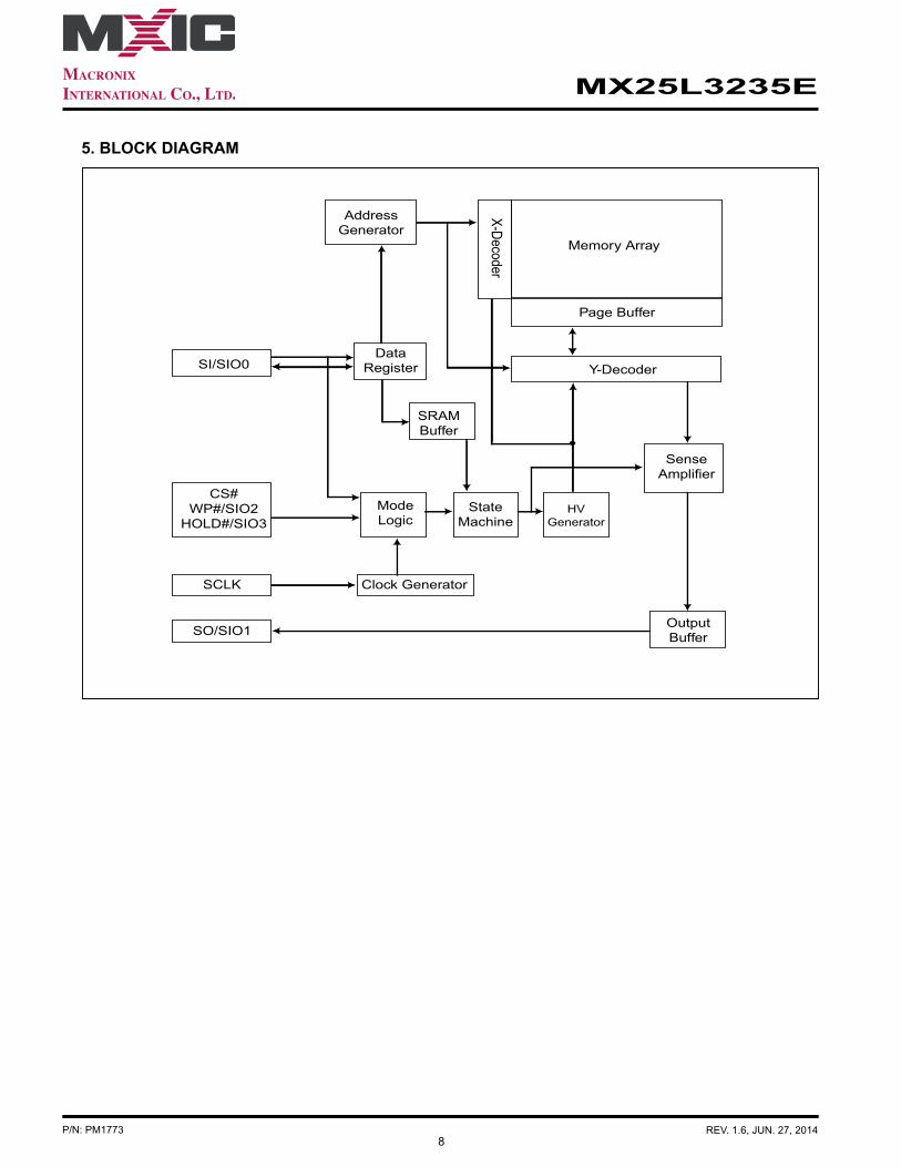
5. BLOCK DIAGRAM
AddressGenerator
Memory Array
Page Buffer
Y-Decoder
X-Decoder
DataRegister
SRAMBuffer
SI/SIO0
SCLK
SO/SIO1
Clock Generator
StateMachine
ModeLogic
SenseAmplifier
HVGenerator
OutputBuffer
CS#WP#/SIO2
HOLD#/SIO3

9
MX25L3235E
P/N: PM1773 REV. 1.6, JUN. 27, 2014
6. DATA PROTECTION
During power transition, there may be some false system level signals which result in inadvertent erasure or programming. The device is designed to protect itself from these accidental write cycles.
The state machine will be reset as standby mode automatically during power up. In addition, the control register architecture of the device constrains that the memory contents can only be changed after specific command sequences have completed successfully.
In the following, there are several features to protect the system from the accidental write cycles during VCC power-up and power-down or from system noise.
• Valid command length checking: The command length will be checked whether it is at byte base and com-pleted on byte boundary.
• Write Enable (WREN) command: WREN command is required to set the Write Enable Latch bit (WEL) before other command to change data. The WEL bit will return to reset stage under following situation:
- Power-up - Write Disable (WRDI) command completion - Write Status Register (WRSR) command completion - Page Program (PP, 4PP) command completion - Continuous Program mode (CP) instruction completion - Sector Erase (SE) command completion - Block Erase (BE, BE32K) command completion - Chip Erase (CE) command completion - Single Block Lock/Unlock (SBLK/SBULK) instruction completion - Gang Block Lock/Unlock (GBLK/GBULK) instruction completion
• Deep Power Down Mode: By entering deep power down mode, the flash device also is under protected from writing all commands except Release from Deep Power Down mode command (RDP) and Read Electronic Signature command (RES).
I. Block lock protection - The Software Protected Mode (SPM) uses (BP3, BP2, BP1, BP0) bits to allow part of memory to be pro-
tected as read only. The protected area definition is shown as table of "Table 2. Protected Area Sizes", the protected areas are more flexible which may protect various areas by setting value of BP0-BP3 bits.
- The Hardware Protected Mode (HPM) uses WP#/SIO2 to protect the (BP3, BP2, BP1, BP0) bits and SRWD
bit. If the system goes into four I/O mode, the feature of HPM will be disabled.
- MX25L3235E provides individual block (or sector) write protect & unprotect. User may enter the mode with WPSEL command and conduct individual block (or sector) write protect with SBLK instruction, or SBULK for individual block (or sector) unprotect. Under the mode, user may conduct whole chip (all blocks) protect with GBLK instruction and unlock the whole chip with GBULK instruction.

10
MX25L3235E
P/N: PM1773 REV. 1.6, JUN. 27, 2014
Table 2. Protected Area SizesProtected Area Sizes (T/B bit = 0)
Status bit Protect LevelBP3 BP2 BP1 BP0 32Mb
0 0 0 0 0 (none)0 0 0 1 1 (1block, block 63rd)0 0 1 0 2 (2blocks, block 62nd-63rd)0 0 1 1 3 (4blocks, block 60th-63rd)0 1 0 0 4 (8blocks, block 56th-63rd)0 1 0 1 5 (16blocks, block 48th-63rd)0 1 1 0 6 (32blocks, block 32nd-63rd)0 1 1 1 7 (64blocks, protect all)1 0 0 0 8 (64blocks, protect all)1 0 0 1 9 (64blocks, protect all)1 0 1 0 10 (64blocks, protect all)1 0 1 1 11 (64blocks, protect all)1 1 0 0 12 (64blocks, protect all)1 1 0 1 13 (64blocks, protect all)1 1 1 0 14 (64blocks, protect all)1 1 1 1 15 (64blocks, protect all)
Protected Area Sizes (T/B bit = 1)Status bit Protect Level
BP3 BP2 BP1 BP0 32Mb0 0 0 0 0 (none)0 0 0 1 1 (1block, block 0th)0 0 1 0 2 (2blocks, block 0th-1st)0 0 1 1 3 (4blocks, block 0th-3rd)0 1 0 0 4 (8blocks, block 0th-7th)0 1 0 1 5 (16blocks, block 0th-15th)0 1 1 0 6 (32blocks, block 0th-31st)0 1 1 1 7 (64blocks, protect all)1 0 0 0 8 (64blocks, protect all)1 0 0 1 9 (64blocks, protect all)1 0 1 0 10 (64blocks, protect all)1 0 1 1 11 (64blocks, protect all)1 1 0 0 12 (64blocks, protect all)1 1 0 1 13 (64blocks, protect all)1 1 1 0 14 (64blocks, protect all)1 1 1 1 15 (64blocks, protect all)
Note: The device is ready to accept a Chip Erase instruction if, and only if, all Block Protect (BP3, BP2, BP1, BP0) are 0.

11
MX25L3235E
P/N: PM1773 REV. 1.6, JUN. 27, 2014
II. Additional 4K-bit secured OTP for unique identifier: to provide 4K-bit One-Time Program area for setting device unique serial number - Which may be set by factory or system maker.
- Security register bit 0 indicates whether the chip is locked by factory or not. - To program the 4K-bit secured OTP by entering 4K-bit secured OTP mode (with ENSO command), and
going through normal program procedure, and then exiting 4K-bit secured OTP mode by writing EXSO com-mand.
- Customer may lock-down the customer lockable secured OTP by writing WRSCUR(write security register) command to set customer lock-down bit1 as "1". Please refer to table of "Table 8. Security Register Defini-tion" for security register bit definition and table of "Table 3. 4K-bit Secured OTP Definition" for address range definition.
Note: Once lock-down whatever by factory or customer, it cannot be changed any more. While in 4K-bit Secured OTP mode, array access is not allowed.
Table 3. 4K-bit Secured OTP Definition
Address range Size Standard Factory Lock Customer Lockxxx000~xxx00F 128-bit ESN (electrical serial number)
Determined by customerxxx010~xxx1FF 3968-bit N/A

12
MX25L3235E
P/N: PM1773 REV. 1.6, JUN. 27, 2014
Table 4. Memory Organization
Block(32K-byte) Sector (4K-byte)1023 3FF000h 3FFFFFh
…
1016 3F8000h 3F8FFFh1015 3F7000h 3F7FFFh
…
1008 3F0000h 3F0FFFh1007 3EF000h 3EFFFFh
…
1000 3E8000h 3E8FFFh999 3E7000h 3E7FFFh
…
992 3E0000h 3E0FFFh991 3DF000h 3DFFFFh
…
984 3D8000h 3D8FFFh983 3D7000h 3D7FFFh
…
976 3D0000h 3D0FFFh
47 02F000h 02FFFFh
…
40 028000h 028FFFh39 027000h 027FFFh
…
32 020000h 020FFFh31 01F000h 01FFFFh
…
24 018000h 018FFFh23 017000h 017FFFh
…
16 010000h 010FFFh15 00F000h 00FFFFh
…
8 008000h 008FFFh7 007000h 007FFFh
…
0 000000h 000FFFh
124
123
122
Address Range
127
126
125
Block(64K-byte)
61
2
1
0
63
62
0
5
4
3
2
1
individual blocklock/unlock unit:64K-byte
individual blocklock/unlock unit:64K-byte
individual blocklock/unlock unit:64K-byte
individual 16 sectorslock/unlock unit:4K-byte
individual 16 sectorslock/unlock unit:4K-byte
7. MEMORY ORGANIZATION

13
MX25L3235E
P/N: PM1773 REV. 1.6, JUN. 27, 2014
8. DEVICE OPERATION
1. Before a command is issued, status register should be checked to ensure device is ready for the intended op-eration.
2. When incorrect command is inputted to this LSI, this LSI becomes standby mode and keeps the standby mode until next CS# falling edge. In standby mode, SO pin of this LSI should be High-Z.
3. When correct command is inputted to this LSI, this LSI becomes active mode and keeps the active mode until next CS# rising edge.
4. For standard single data rate serial mode, input data is latched on the rising edge of Serial Clock(SCLK) and data shifts out on the falling edge of SCLK. The difference of Serial mode 0 and mode 3 is shown as "Figure 1. Serial Modes Supported (for Normal Serial mode)".
5. For the following instructions: RDID, RDSR, RDSCUR, READ, FAST_READ, RDSFDP, 2READ, DREAD, 4READ, QREAD, RDBLOCK, RES, REMS, REMS2, and REMS4 the shifted-in instruction sequence is fol-lowed by a data-out sequence. After any bit of data being shifted out, the CS# can be high. For the follow-ing instructions: WREN, WRDI, WRSR, SE, BE, BE32K, HPM, CE, PP, CP, 4PP, RDP, DP, WPSEL, SBLK, SBULK, GBLK, GBULK, ENSO, EXSO, WRSCUR, ESRY and DSRY. The CS# must go high exactly at the byte boundary; otherwise, the instruction will be rejected and not executed.
6. During the progress of Write Status Register, Program, Erase operation, to access the memory array is ne-glected and not affect the current operation of Write Status Register, Program, Erase.
Note:CPOL indicates clock polarity of Serial master, CPOL=1 for SCLK high while idle, CPOL=0 for SCLK low while not transmitting. CPHA indicates clock phase. The combination of CPOL bit and CPHA bit decides which Serial mode is supported.
Figure 1. Serial Modes Supported (for Normal Serial mode)
SCLK
MSB
CPHA shift in shift out
SI
0
1
CPOL
0(Serial mode 0)
(Serial mode 3) 1
SO
SCLK
MSB

14
MX25L3235E
P/N: PM1773 REV. 1.6, JUN. 27, 2014
9. HOLD FEATURE
HOLD# pin signal goes low to hold any serial communications with the device. The HOLD feature will not stop the operation of write status register, programming, or erasing in progress.
The operation of HOLD requires Chip Select (CS#) keeping low and starts on falling edge of HOLD# pin signal while Serial Clock (SCLK) signal is being low (if Serial Clock signal is not being low, HOLD operation will not start until Serial Clock signal being low). The HOLD condition ends on the rising edge of HOLD# pin signal while Serial Clock(SCLK) signal is being low( if Serial Clock signal is not being low, HOLD operation will not end until Serial Clock being low).
Figure 2. Hold Condition Operation
HOLD#
CS#
SCLK
HoldCondition
(standard)
HoldCondition
(non-standard)
The Serial Data Output (SO) is high impedance, both Serial Data Input (SI) and Serial Clock (SCLK) are don't care during the HOLD operation. If Chip Select (CS#) drives high during HOLD operation, it will reset the internal logic of the device. To re-start communication with chip, the HOLD# must be at high and CS# must be at low.
Note: The HOLD feature is disabled during Quad I/O mode.
15
MX25L3235E
P/N: PM1773 REV. 1.6, JUN. 27, 2014
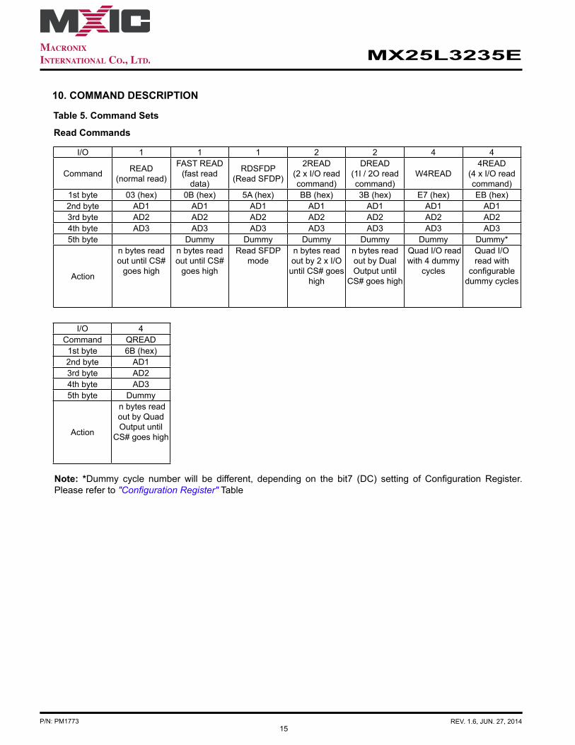
10. COMMAND DESCRIPTION
Table 5. Command Sets
Read Commands
Note: *Dummy cycle number will be different, depending on the bit7 (DC) setting of Configuration Register. Please refer to "Configuration Register" Table
I/O 1 1 1 2 2 4 4
Command READ (normal read)
FAST READ (fast read
data)
RDSFDP(Read SFDP)
2READ (2 x I/O read command)
DREAD (1I / 2O read command)
W4READ4READ
(4 x I/O read command)
1st byte 03 (hex) 0B (hex) 5A (hex) BB (hex) 3B (hex) E7 (hex) EB (hex)2nd byte AD1 AD1 AD1 AD1 AD1 AD1 AD13rd byte AD2 AD2 AD2 AD2 AD2 AD2 AD2 4th byte AD3 AD3 AD3 AD3 AD3 AD3 AD3 5th byte Dummy Dummy Dummy Dummy Dummy Dummy*
Action
n bytes read out until CS#
goes high
n bytes read out until CS#
goes high
Read SFDPmode
n bytes read out by 2 x I/O
until CS# goes high
n bytes read out by Dual Output until
CS# goes high
Quad I/O read with 4 dummy
cycles
Quad I/O read with
configurable dummy cycles
I/O 4Command QREAD1st byte 6B (hex)2nd byte AD13rd byte AD2 4th byte AD3 5th byte Dummy
Action
n bytes read out by Quad Output until
CS# goes high
16
MX25L3235E
P/N: PM1773 REV. 1.6, JUN. 27, 2014
Other Commands
Command WREN(write enable)
WRDI(write disable)
RDSR (read status register)
RDCR (read configuration
register)
WRSR (write status/ configuration
register)
4PP (quad page program)
SE (sector erase)
1st byte 06 (hex) 04 (hex) 05 (hex) 15 (hex) 01 (hex) 38 (hex) 20 (hex)2nd byte Values AD1 AD13rd byte Values AD2 AD24th byte AD3 AD3
Action
sets the (WEL) write enable
latch bit
resets the (WEL) write enable latch
bit
to read out the values of the
status register
to read out the values of the configuration
register
to write new values of the
status register
quad input to program the
selected page
to erase the selected sector
Command BE 32K (block erase 32KB)
BE (block erase 64KB)
CE (chip erase)
PP (page program)
CP (continuous program)
DP (Deep power down)
RDP (Release from deep
power down)1st byte 52 (hex) D8 (hex) 60 or C7 (hex) 02 (hex) AD (hex) B9 (hex) AB (hex)2nd byte AD1 AD1 AD1 AD1 3rd byte AD2 AD2 AD2 AD2 4th byte AD3 AD3 AD3 AD3
Action
to erase the selected 32KB
block
to erase the selected 64KB
block
to erase whole chip
to program the selected page
continuously program
whole chip, the address is automatically
increase
enters deep power down
mode
release from deep power down mode
Command RDID (read identific-
ation)
RES (read electronic ID)
REMS (read electronic
manufacturer & device ID)
REMS2 (read electronic
manufacturer & device ID)
REMS4 (read electronic
manufacturer & device ID)
ENSO (enter secured OTP)
1st byte 9F (hex) AB (hex) 90 (hex) EF (hex) DF (hex) B1 (hex)2nd byte x x x x 3rd byte x x x x 4th byte x ADD (Note 2) ADD ADD
Action
outputs JEDEC
ID: 1-byte Manufacturer ID & 2-byte Device ID
to read out 1-byte Device
ID
output the Manufacturer
ID & Device ID
output the Manufacturer
ID & Device ID
output the Manufacturer ID & device ID
to enter the 4K-bit secured
OTP mode

17
MX25L3235E
P/N: PM1773 REV. 1.6, JUN. 27, 2014
Command EXSO (exit secured OTP)
RDSCUR (read security
register)
WRSCUR (write security
register)
SBLK (single block lock
SBULK (single block unlock)
RDBLOCK (block protect
read)
GBLK (gang block lock)
1st byte C1 (hex) 2B (hex) 2F (hex) 36 (hex) 39 (hex) 3C (hex) 7E (hex)2nd byte AD1 AD1 AD13rd byte AD2 AD2 AD24th byte AD3 AD3 AD3
Action
to exit the 4K-bit secured OTP mode
to read value of security
register
to set the lock-down bit as
"1" (once lock-down, cannot
be update)
individual block
(64K-byte) or sector
(4K-byte) write protect
individual block
(64K-byte) or sector (4K-byte) unprotect
read individual block or sector write protect
status
whole chip write protect
Note 1: The count base is 4-bit for ADD(2) and Dummy(2) because of 2 x I/O. And the MSB is on SI/SIO1 which is different from 1 x I/O condition.
Note 2: ADD=00H will output the manufacturer ID first and ADD=01H will output device ID first.Note 3: It is not recommended to adopt any other code not in the command definition table, which will potentially enter the
hidden mode.Note 4: Before executing RST command, RSTEN command must be executed. If there is any other command to interfere,
the reset operation will be disabled.
COMMAND GBULK (gang block unlock)
NOP (No Operation)
RSTEN(Reset Enable)
RST(Reset
Memory)
WPSEL(Write Protect
Selection)
ESRY (enable SO to output
RY/BY#)
DSRY (disable SO to output
RY/BY#)1st byte 98 (hex) 00 (hex) 66 (hex) 99 (hex) 68 (hex) 70 (hex) 80 (hex)2nd byte 3rd byte 4th byte Action whole chip
unprotectto enter
and enable individal block protect mode
to enable SO to output RY/
BY# during CP mode
to disable SO to output RY/
BY# during CP mode
COMMAND Release Read Enhanced
1st byte FF (hex)2nd byte3rd byte4th byte5th byteAction All these
commands FFh, 00h, AAh
or 55h will escape the
performance mode
18
MX25L3235E
P/N: PM1773 REV. 1.6, JUN. 27, 2014
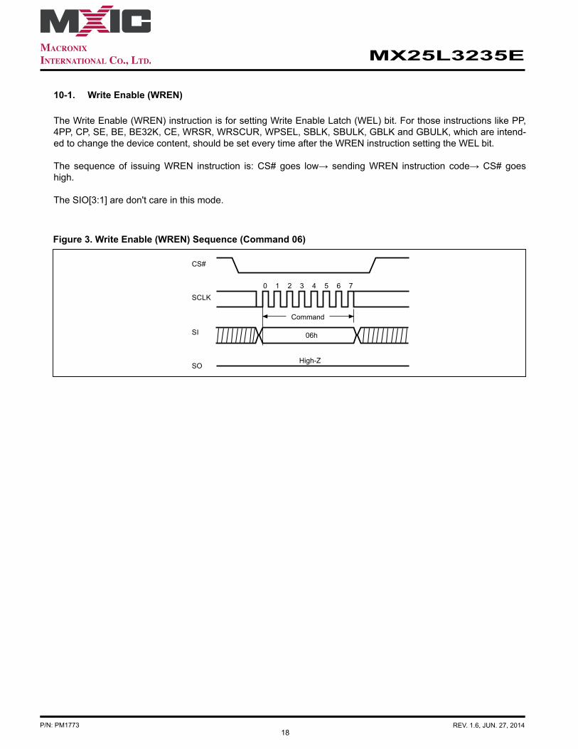
10-1. Write Enable (WREN)
The Write Enable (WREN) instruction is for setting Write Enable Latch (WEL) bit. For those instructions like PP, 4PP, CP, SE, BE, BE32K, CE, WRSR, WRSCUR, WPSEL, SBLK, SBULK, GBLK and GBULK, which are intend-ed to change the device content, should be set every time after the WREN instruction setting the WEL bit.
The sequence of issuing WREN instruction is: CS# goes low→ sending WREN instruction code→ CS# goes high.
The SIO[3:1] are don't care in this mode.
Figure 3. Write Enable (WREN) Sequence (Command 06)
21 3 4 5 6 7
High-Z
0
06h
Command
SCLK
SI
CS#
SO
19
MX25L3235E
P/N: PM1773 REV. 1.6, JUN. 27, 2014
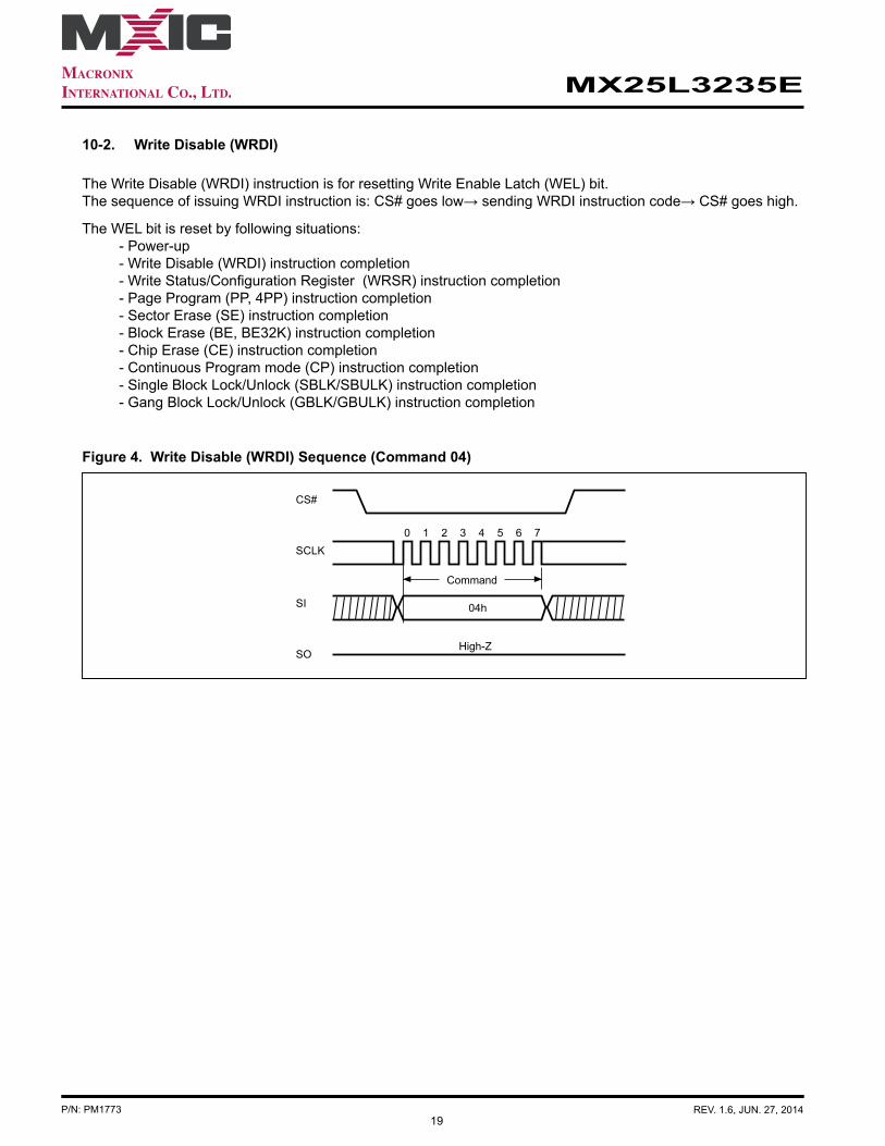
10-2. Write Disable (WRDI)
The Write Disable (WRDI) instruction is for resetting Write Enable Latch (WEL) bit.The sequence of issuing WRDI instruction is: CS# goes low→ sending WRDI instruction code→ CS# goes high.
The WEL bit is reset by following situations: - Power-up - Write Disable (WRDI) instruction completion - Write Status/Configuration Register (WRSR) instruction completion - Page Program (PP, 4PP) instruction completion - Sector Erase (SE) instruction completion - Block Erase (BE, BE32K) instruction completion - Chip Erase (CE) instruction completion - Continuous Program mode (CP) instruction completion - Single Block Lock/Unlock (SBLK/SBULK) instruction completion - Gang Block Lock/Unlock (GBLK/GBULK) instruction completion
Figure 4. Write Disable (WRDI) Sequence (Command 04)
21 3 4 5 6 7
High-Z
0
04h
Command
SCLK
SI
CS#
SO

20
MX25L3235E
P/N: PM1773 REV. 1.6, JUN. 27, 2014
Figure 5. Read Identification (RDID) Sequence (Command 9F)
10-3. Read Identification (RDID)
The RDID instruction is for reading the Manufacturer ID of 1-byte and followed by Device ID of 2-byte. The Macronix Manufacturer ID is C2(hex), the memory type ID is 20(hex) as the first-byte Device ID, and the in-dividual Device ID of second-byte ID are listed as table of "Table 7. ID Definitions".
The sequence of issuing RDID instruction is: CS# goes low→ sending RDID instruction code → 24-bits ID data out on SO→ to end RDID operation can use CS# to high at any time during data out.
While Program/Erase operation is in progress, it will not decode the RDID instruction, so there's no effect on the cycle of program/erase operation which is currently in progress. When CS# goes high, the device is at standby stage.
21 3 4 5 6 7 8 9 10 11 12 13 14 15
Command
0
Manufacturer IdentificationHigh-Z
MSB
15 14 13 3 2 1 0
Device Identification
MSB
7 6 5 3 2 1 0
16 17 18 28 29 30 31SCLK
SI
CS#
SO
9Fh
21
MX25L3235E
P/N: PM1773 REV. 1.6, JUN. 27, 2014
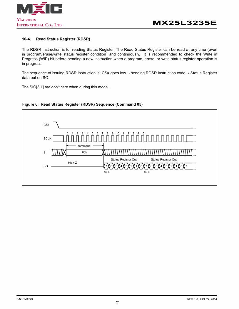
10-4. Read Status Register (RDSR)
The RDSR instruction is for reading Status Register. The Read Status Register can be read at any time (even in program/erase/write status register condition) and continuously. It is recommended to check the Write in Progress (WIP) bit before sending a new instruction when a program, erase, or write status register operation is in progress.
The sequence of issuing RDSR instruction is: CS# goes low→ sending RDSR instruction code→ Status Register data out on SO.
The SIO[3:1] are don't care when during this mode.
Figure 6. Read Status Register (RDSR) Sequence (Command 05)
21 3 4 5 6 7 8 9 10 11 12 13 14 15
command
0
7 6 5 4 3 2 1 0
Status Register OutHigh-Z
MSB
7 6 5 4 3 2 1 0
Status Register Out
MSB
7
SCLK
SI
CS#
SO
05h
22
MX25L3235E
P/N: PM1773 REV. 1.6, JUN. 27, 2014
The definition of the status register bits is as below:
WIP bit. The Write in Progress (WIP) bit, a volatile bit, indicates whether the device is busy in program/erase/write status register progress. When WIP bit sets to 1, which means the device is busy in program/erase/write status register progress. When WIP bit sets to 0, which means the device is not in progress of program/erase/write status register cycle.
WEL bit. The Write Enable Latch (WEL) bit, a volatile bit, indicates whether the device is set to internal write en-able latch. When WEL bit sets to "1", which means the internal write enable latch is set, the device can accept program/erase/write status register instruction. When WEL bit sets to 0, which means no internal write enable latch; the device will not accept program/erase/write status register instruction. The program/erase command will be ignored and will reset WEL bit if it is applied to a protected memory area. To ensure both WIP bit & WEL bit are both set to 0 and available for next program/erase/operations, WIP bit needs to be confirm to be 0 before polling WEL bit. After WIP bit confirmed, WEL bit needs to be confirm to be 0.
BP3, BP2, BP1, BP0 bits. The Block Protect (BP3, BP2, BP1, BP0) bits, non-volatile bits, indicate the protect-ed area (as defined in "Table 2. Protected Area Sizes") of the device to against the program/erase instruction without hardware protection mode being set. To write the Block Protect (BP3, BP2, BP1, BP0) bits requires the Write Status Register (WRSR) instruction to be executed. Those bits define the protected area of the memory to against Page Program (PP), Sector Erase (SE), Block Erase (BE) and Chip Erase (CE) instructions (only if all Block Protect bits set to 0, the CE instruction can be executed). The BP3, BP2, BP1, BP0 bits are "0" as default. Which is un-protected.
QE bit. The Quad Enable (QE) bit, non-volatile bit, while it is "0" (factory default), it performs non-Quad and WP# is enable. While QE is "1", it performs Quad I/O mode and WP# is disabled. In the other word, if the system goes into four I/O mode (QE=1), the feature of HPM will be disabled.
SRWD bit. The Status Register Write Disable (SRWD) bit, non-volatile bit, default value is "0". SRWD bit is oper-ated together with Write Protection (WP#/SIO2) pin for providing hardware protection mode. The hardware pro-tection mode requires SRWD sets to 1 and WP#/SIO2 pin signal is low stage. In the hardware protection mode, the Write Status Register (WRSR) instruction is no longer accepted for execution and the SRWD bit and Block Protect bits (BP3, BP2, BP1, BP0) are read only. The SRWD bit defaults to be "0".
Status Register
Note: See the "Table 2. Protected Area Sizes" .
bit7 bit6 bit5 bit4 bit3 bit2 bit1 bit0SRWD (status
register write protect)
QE(Quad
Enable)
BP3 (level of
protected block)
BP2 (level of
protected block)
BP1 (level of
protected block)
BP0 (level of
protected block)
WEL(write enable
latch)
WIP(write in
progress bit)
1=status register write
disable
1= Quad Enable
0=not Quad Enable
(note 1) (note 1) (note 1) (note 1)
1=write enable
0=not write enable
1=write operation
0=not in write operation
Non-volatile bit
Non-volatile bit
Non-volatile bit
Non-volatile bit
Non-volatile bit
Non-volatile bit volatile bit volatile bit
23
MX25L3235E
P/N: PM1773 REV. 1.6, JUN. 27, 2014
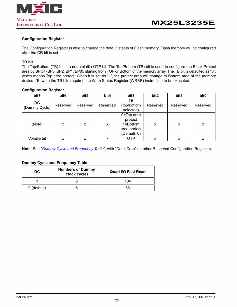
Configuration Register
The Configuration Register is able to change the default status of Flash memory. Flash memory will be configured after the CR bit is set.
TB bitThe Top/Bottom (TB) bit is a non-volatile OTP bit. The Top/Bottom (TB) bit is used to configure the Block Protect area by BP bit (BP3, BP2, BP1, BP0), starting from TOP or Bottom of the memory array. The TB bit is defaulted as “0”, which means Top area protect. When it is set as “1”, the protect area will change to Bottom area of the memory device. To write the TB bits requires the Write Status Register (WRSR) instruction to be executed.
Configuration Registerbit7 bit6 bit5 bit4 bit3 bit2 bit1 bit0
DC(Dummy Cycle) Reserved Reserved Reserved
TB (top/bottom selected)
Reserved Reserved Reserved
(Note) x x x
0=Top area protect
1=Bottom area protect (Default=0)
x x x
Volatile bit x x x OTP x x x
Note: See "Dummy Cycle and Frequency Table", with "Don't Care" on other Reserved Configuration Registers.
Dummy Cycle and Frequency Table
DC Numbers of Dummy clock cycles Quad I/O Fast Read
1 8 104
0 (default) 6 86
24
MX25L3235E
P/N: PM1773 REV. 1.6, JUN. 27, 2014
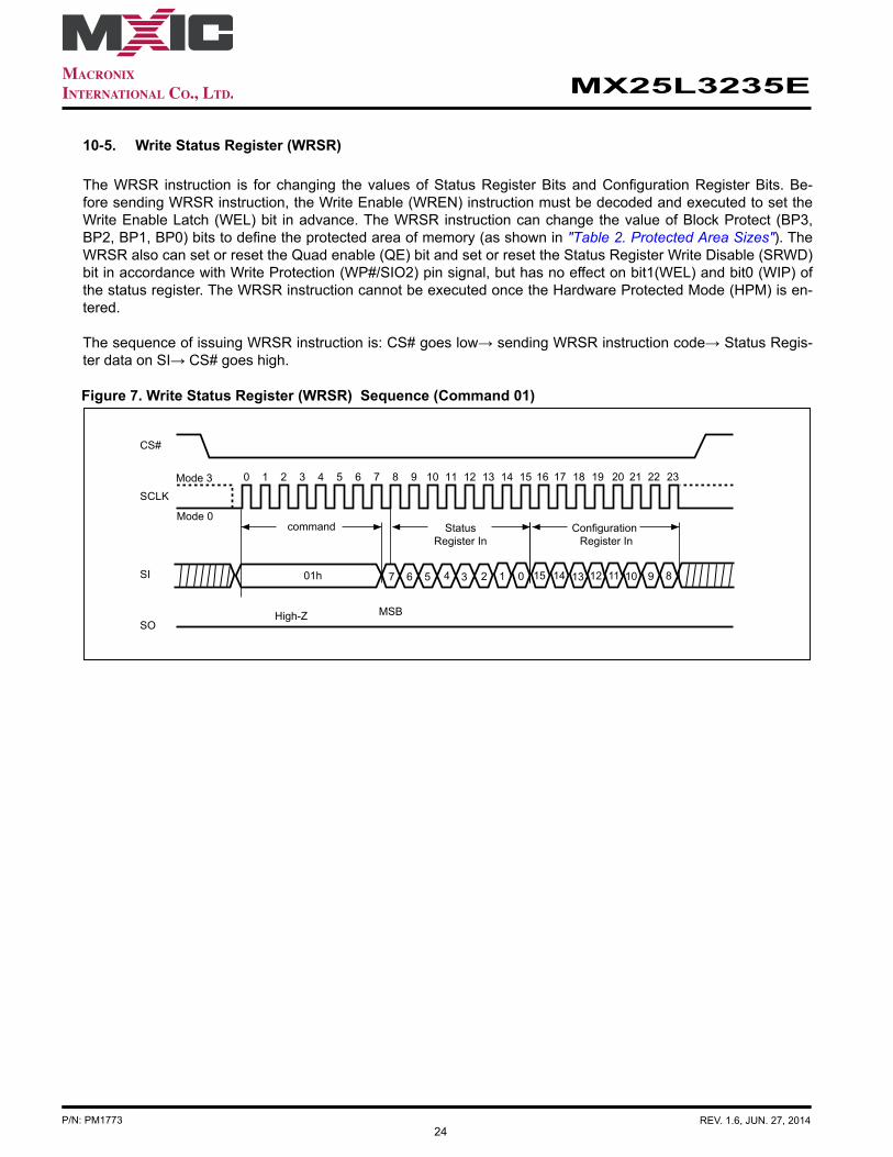
10-5. Write Status Register (WRSR)
The WRSR instruction is for changing the values of Status Register Bits and Configuration Register Bits. Be-fore sending WRSR instruction, the Write Enable (WREN) instruction must be decoded and executed to set the Write Enable Latch (WEL) bit in advance. The WRSR instruction can change the value of Block Protect (BP3, BP2, BP1, BP0) bits to define the protected area of memory (as shown in "Table 2. Protected Area Sizes"). The WRSR also can set or reset the Quad enable (QE) bit and set or reset the Status Register Write Disable (SRWD) bit in accordance with Write Protection (WP#/SIO2) pin signal, but has no effect on bit1(WEL) and bit0 (WIP) of the status register. The WRSR instruction cannot be executed once the Hardware Protected Mode (HPM) is en-tered.
The sequence of issuing WRSR instruction is: CS# goes low→ sending WRSR instruction code→ Status Regis-ter data on SI→ CS# goes high.
Figure 7. Write Status Register (WRSR) Sequence (Command 01)
21 3 4 5 6 7 8 9 10 11 12 13 14 15
StatusRegister In
ConfigurationRegister In
0
MSB
SCLK
SI
CS#
SO
01h
High-Z
command
Mode 3
Mode 0
16 17 18 19 20 21 22 23
7 6 5 4 3 2 1 0 15 14 13 12 11 10 9 8

25
MX25L3235E
P/N: PM1773 REV. 1.6, JUN. 27, 2014
The CS# must go high exactly at the byte boundary; otherwise, the instruction will be rejected and not executed. The self-timed Write Status Register cycle time (tW) is initiated as soon as Chip Select (CS#) goes high. The Write in Progress (WIP) bit still can be checked out during the Write Status Register cycle is in progress. The WIP sets 1 during the tW timing, and sets 0 when Write Status Register Cycle is completed, and the Write En-able Latch (WEL) bit is reset.
Note: As defined by the values in the Block Protect (BP3, BP2, BP1, BP0) bits of the Status Register, as shown in "Table 2. Protected Area Sizes".
Mode Status register condition WP# and SRWD bit status Memory
Software protectionmode (SPM)
Status register can be writtenin (WEL bit is set to "1") and
the SRWD, BP0-BP3bits can be changed
WP#=1 and SRWD bit=0, orWP#=0 and SRWD bit=0, or
WP#=1 and SRWD=1
The protected area cannotbe programmed or erased.
Hardware protectionmode (HPM)
The SRWD, BP0-BP3 ofstatus register bits cannot be
changedWP#=0, SRWD bit=1 The protected area cannot
be programmed or erased.
Table 6. Protection Modes
As the table above showing, the summary of the Software Protected Mode (SPM) and Hardware Protected Mode (HPM):
Software Protected Mode (SPM): - When SRWD bit=0, no matter WP#/SIO2 is low or high, the WREN instruction may set the WEL bit and can
change the values of SRWD, BP3, BP2, BP1, BP0. The protected area, which is defined by BP3, BP2, BP1, BP0, is at software protected mode (SPM).
- When SRWD bit=1 and WP#/SIO2 is high, the WREN instruction may set the WEL bit can change the values of SRWD, BP3, BP2, BP1, BP0. The protected area, which is defined by BP3, BP2, BP1, BP0, is at software protected mode (SPM)
Hardware Protected Mode (HPM):- When SRWD bit=1, and then WP#/SIO2 is low (or WP#/SIO2 is low before SRWD bit=1), it enters the hard-
ware protected mode (HPM). The data of the protected area is protected by software protected mode by BP3, BP2, BP1, BP0 and hardware protected mode by the WP#/SIO2 to against data modification.
Note: To exit the hardware protected mode requires WP#/SIO2 driving high once the hardware protected mode is entered. If the WP#/SIO2 pin is permanently connected to high, the hardware protected mode can never be en-tered; only can use software protected mode via BP3, BP2, BP1, BP0.If the system goes into four I/O mode, the feature of HPM will be disabled.

26
MX25L3235E
P/N: PM1773 REV. 1.6, JUN. 27, 2014
Figure 8. WRSR flow
WREN command
WRSR command
Write status register data
RDSR command
WRSR successfully
Yes
YesWRSR fail
No
start
Verify OK?
WIP=0?No
RDSR command
Yes
WEL=1?No
RDSR command
Read WEL=0, BP[3:0], QE, and SRWD data
27
MX25L3235E
P/N: PM1773 REV. 1.6, JUN. 27, 2014
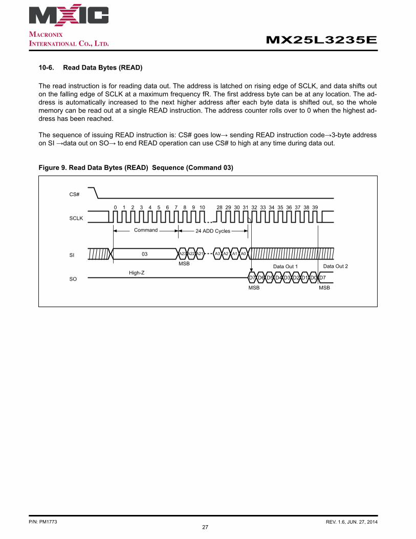
10-6. Read Data Bytes (READ)
The read instruction is for reading data out. The address is latched on rising edge of SCLK, and data shifts out on the falling edge of SCLK at a maximum frequency fR. The first address byte can be at any location. The ad-dress is automatically increased to the next higher address after each byte data is shifted out, so the whole memory can be read out at a single READ instruction. The address counter rolls over to 0 when the highest ad-dress has been reached.
The sequence of issuing READ instruction is: CS# goes low→ sending READ instruction code→3-byte address on SI →data out on SO→ to end READ operation can use CS# to high at any time during data out.
Figure 9. Read Data Bytes (READ) Sequence (Command 03)
SCLK
SI
CS#
SO
21 3 4 5 6 7 8 9 10 28 29 30 31 32 33 34 35 36 37 38
Data Out 1
24 ADD Cycles
0
MSB MSB
MSB
39
Data Out 2
03
High-Z
Command
D7
A23 A22 A21 A3 A2 A1 A0
D7D6 D5 D4 D3 D2 D1 D0

28
MX25L3235E
P/N: PM1773 REV. 1.6, JUN. 27, 2014
10-7. Read Data Bytes at Higher Speed (FAST_READ)
The FAST_READ instruction is for quickly reading data out. The address is latched on rising edge of SCLK, and data of each bit shifts out on the falling edge of SCLK at a maximum frequency fC. The first address byte can be at any location. The address is automatically increased to the next higher address after each byte data is shifted out, so the whole memory can be read out at a single FAST_READ instruction. The address counter rolls over to 0 when the highest address has been reached.
The sequence of issuing FAST_READ instruction is: CS# goes low→ sending FAST_READ instruction code→ 3-byte address on SI→1-dummy byte (default) address on SI→ data out on SO→ to end FAST_READ operation can use CS# to high at any time during data out.
In the performance-enhancing mode, P[7:4] must be toggling with P[3:0] ; likewise P[7:0]=A5h,5Ah,F0h or 0Fh can make this mode continue and reduce the next 4READ instruction. Once P[7:4] is no longer toggling with P[3:0]; likewise P[7:0]=FFh,00h,AAh or 55h and afterwards CS# is raised and then lowered, the system then will escape from performance enhance mode and return to normal operation.
While Program/Erase/Write Status Register cycle is in progress, FAST_READ instruction is rejected without any impact on the Program/Erase/Write Status Register current cycle.
Figure 10. Read at Higher Speed (FAST_READ) Sequence (Command 0B) (104MHz)
23
21 3 4 5 6 7 8 9 10 28 29 30 31
22 21 3 2 1 0
High-Z
24 BIT ADDRESS
0
32 33 34 36 37 38 39 40 41 42 43 44 45 46
7 6 5 4 3 2 01
DATA OUT 1
Dummy Cycle
MSB
7 6 5 4 3 2 1 0
DATA OUT 2
MSB MSB
7
47
7 6 5 4 3 2 01
35
SCLK
SI
CS#
SO
SCLK
SI
CS#
SO
0Bh
Command
29
MX25L3235E
P/N: PM1773 REV. 1.6, JUN. 27, 2014
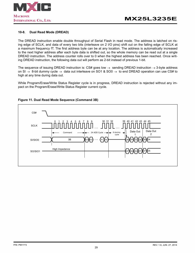
10-8. Dual Read Mode (DREAD)
The DREAD instruction enable double throughput of Serial Flash in read mode. The address is latched on ris-ing edge of SCLK, and data of every two bits (interleave on 2 I/O pins) shift out on the falling edge of SCLK at a maximum frequency fT. The first address byte can be at any location. The address is automatically increased to the next higher address after each byte data is shifted out, so the whole memory can be read out at a single DREAD instruction. The address counter rolls over to 0 when the highest address has been reached. Once writ-ing DREAD instruction, the following data out will perform as 2-bit instead of previous 1-bit.
The sequence of issuing DREAD instruction is: CS# goes low → sending DREAD instruction → 3-byte address on SI → 8-bit dummy cycle → data out interleave on SO1 & SO0 → to end DREAD operation can use CS# to high at any time during data out.
While Program/Erase/Write Status Register cycle is in progress, DREAD instruction is rejected without any im-pact on the Program/Erase/Write Status Register current cycle.
Figure 11. Dual Read Mode Sequence (Command 3B)
High Impedance
21 3 4 5 6 7 80
SCLK
SI/SIO0
SO/SIO1
CS#
9 30 31 32 39 40 41 43 44 4542
3B D4
D5
D2
D3D7
D6 D6 D4D0
D7 D5D1
Command 24 ADD Cycle 8 dummy cycle
A23 A22 A1 A0
… …
…
Data Out1
Data Out2
30
MX25L3235E
P/N: PM1773 REV. 1.6, JUN. 27, 2014
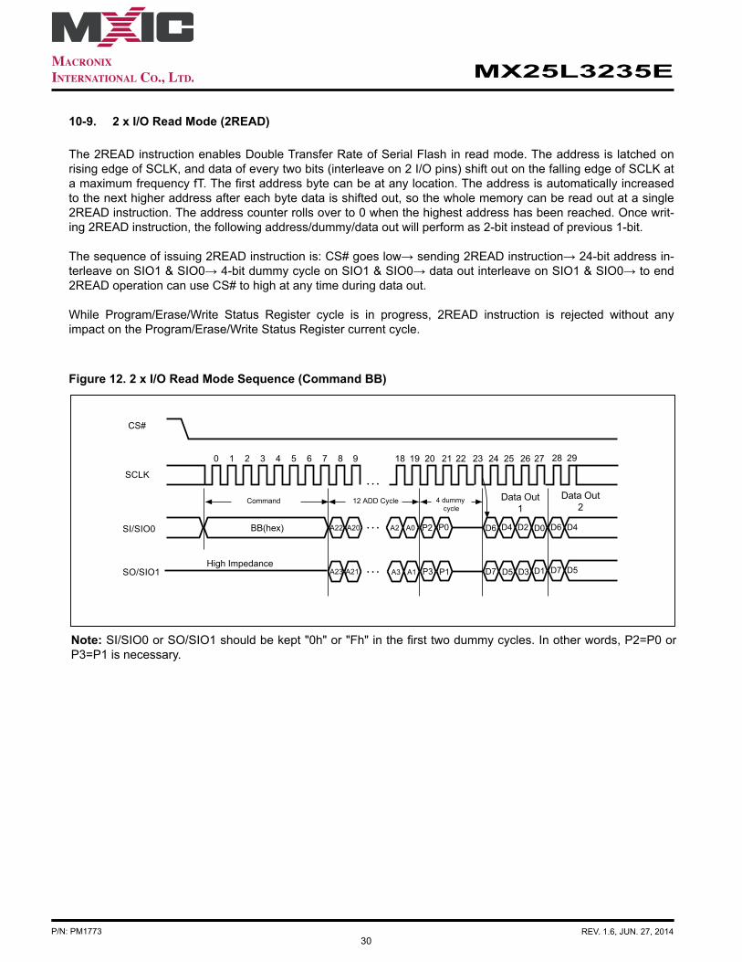
10-9. 2 x I/O Read Mode (2READ)
The 2READ instruction enables Double Transfer Rate of Serial Flash in read mode. The address is latched on rising edge of SCLK, and data of every two bits (interleave on 2 I/O pins) shift out on the falling edge of SCLK at a maximum frequency fT. The first address byte can be at any location. The address is automatically increased to the next higher address after each byte data is shifted out, so the whole memory can be read out at a single 2READ instruction. The address counter rolls over to 0 when the highest address has been reached. Once writ-ing 2READ instruction, the following address/dummy/data out will perform as 2-bit instead of previous 1-bit.
The sequence of issuing 2READ instruction is: CS# goes low→ sending 2READ instruction→ 24-bit address in-terleave on SIO1 & SIO0→ 4-bit dummy cycle on SIO1 & SIO0→ data out interleave on SIO1 & SIO0→ to end 2READ operation can use CS# to high at any time during data out.
While Program/Erase/Write Status Register cycle is in progress, 2READ instruction is rejected without any impact on the Program/Erase/Write Status Register current cycle.
Figure 12. 2 x I/O Read Mode Sequence (Command BB)
High Impedance
21 3 4 5 6 7 80
SCLK
SI/SIO0
SO/SIO1
CS#
9 18 19 20
BB(hex)
21 22 23 24 25 26 27 28 29
P0P2
P1P3
D4
D5
D2
D3D7
D6 D6 D4D0
D7 D5D1
Command 12 ADD Cycle 4 dummy cycle
A22 A20 A2 A0
A3 A1A23 A21
…
…
…
Data Out1
Data Out2
Note: SI/SIO0 or SO/SIO1 should be kept "0h" or "Fh" in the first two dummy cycles. In other words, P2=P0 or P3=P1 is necessary.
31
MX25L3235E
P/N: PM1773 REV. 1.6, JUN. 27, 2014
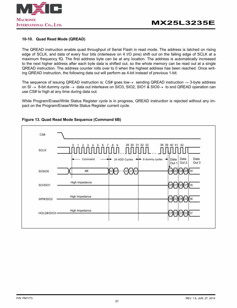
10-10. Quad Read Mode (QREAD)
The QREAD instruction enable quad throughput of Serial Flash in read mode. The address is latched on rising edge of SCLK, and data of every four bits (interleave on 4 I/O pins) shift out on the falling edge of SCLK at a maximum frequency fQ. The first address byte can be at any location. The address is automatically increased to the next higher address after each byte data is shifted out, so the whole memory can be read out at a single QREAD instruction. The address counter rolls over to 0 when the highest address has been reached. Once writ-ing QREAD instruction, the following data out will perform as 4-bit instead of previous 1-bit.
The sequence of issuing QREAD instruction is: CS# goes low→ sending QREAD instruction → 3-byte address on SI → 8-bit dummy cycle → data out interleave on SIO3, SIO2, SIO1 & SIO0→ to end QREAD operation can use CS# to high at any time during data out.
While Program/Erase/Write Status Register cycle is in progress, QREAD instruction is rejected without any im-pact on the Program/Erase/Write Status Register current cycle.
Figure 13. Quad Read Mode Sequence (Command 6B)
High Impedance
21 3 4 5 6 7 80
SCLK
SI/SIO0
SO/SIO1
CS#
299 30 31 32 33 38 39 40 41 42
6B
High ImpedanceWP#/SIO2
High ImpedanceHOLD#/SIO3
8 dummy cycles
D4 D0
D5 D1
D6 D2
D7 D3
D4 D0
D5 D1
D6 D2
D7 D3
D4
D5
D6
D7
A23A22 A2 A1 A0
Command 24 ADD Cycles Data Out 1
Data Out 2
Data Out 3
…
…
…

32
MX25L3235E
P/N: PM1773 REV. 1.6, JUN. 27, 2014
10-11. 4 x I/O Read Mode (4READ)
The 4READ instruction enables quad throughput of Serial Flash in read mode. A Quad Enable (QE) bit of sta-tus Register must be set to "1" before sending the 4READ instruction. The address is latched on rising edge of SCLK, and data of every four bits (interleave on 4 I/O pins) shift out on the falling edge of SCLK at a maximum frequency fQ. The first address byte can be at any location. The address is automatically increased to the next higher address after each byte data is shifted out, so the whole memory can be read out at a single 4READ in-struction. The address counter rolls over to 0 when the highest address has been reached. Once writing 4READ instruction, the following address/dummy/data out will perform as 4-bit instead of previous 1-bit.
The sequence of issuing 4READ instruction is: CS# goes low→ sending 4READ instruction→ 24-bit address in-terleave on SIO3, SIO2, SIO1 & SIO0→2+4 dummy cycles (default)→data out interleave on SIO3, SIO2, SIO1 & SIO0→ to end 4READ operation can use CS# to high at any time during data out.
W4READ instruction (E7) is also available for 4 I/O read. The sequence is similar to 4READ, but with only 4 dummy cycles. The clock rate runs at 54MHz.
Figure 14. 4 x I/O Read Mode Sequence (Command EB)
High Impedance
21 3 4 5 6 7 80
SCLK
SI/SIO0
SO/SIO1
CS#
9 1210 11 13 14
EBh addressbit20, bit16..bit0
addressbit21, bit17..bit1
P4 P0
P5 P1
P6 P2
P7 P3
databit4, bit0, bit4....
databit5 bit1, bit5....
15 16 17 18 19 20 21 22 23 n
High ImpedanceWP#/SIO2
addressbit22, bit18..bit2
databit6 bit2, bit6....
High ImpedanceHOLD#/SIO3 address
bit23, bit19..bit3data
bit7 bit3, bit7....
8 Bit Instruction 6 Address cyclesCon�gurable
Dummy cyclesPerformance
enhance indicator (Note 2)
Data Output(Note 3)
Note:1. Hi-impedance is inhibited for the two clock cycles.2. P7≠P3, P6≠P2, P5≠P1 & P4≠P0 (Toggling) is inhibited.3. The Configurable Dummy Cycle is set by Configuration Register Bit. Please see "Dummy Cycle and Fre-
quency Table"

33
MX25L3235E
P/N: PM1773 REV. 1.6, JUN. 27, 2014
Another sequence of issuing 4READ instruction especially useful in random access is : CS# goes low→ sending 4READ instruction→ 3-bytes address interleave on SIO3, SIO2, SIO1 & SIO0 →performance enhance toggling bit P[7:0]→ 4 dummy cycles (default)→ data out still CS# goes high → CS# goes low (reduce 4 Read instruc-tion) → 24-bit random access address (Please refer to "Figure 15. 4 x I/O Read enhance performance Mode Se-quence (Command EB)").
In the performance-enhancing mode (Notes of "Figure 15. 4 x I/O Read enhance performance Mode Sequence (Command EB)"), P[7:4] must be toggling with P[3:0]; likewise P[7:0]=A5h, 5Ah, F0h or 0Fh can make this mode continue and reduce the next 4READ instruction. Once P[7:4] is no longer toggling with P[3:0]; likewise P[7:0]=FFh, 00h, AAh or 55h. These commands will reset the performance enhance mode. And afterwards CS# is raised and then lowered, the system then will return to normal operation.
While Program/Erase/Write Status Register cycle is in progress, 4READ instruction is rejected without any im-pact on the Program/Erase/Write Status Register current cycle.
10-12. Performance Enhance Mode
The device could waive the command cycle bits if the two cycle bits after address cycle toggles. (Please note "Figure 15. 4 x I/O Read enhance performance Mode Sequence (Command EB)")
Please be noticed that “EBh” and “E7h” commands support enhance mode. The performance enhance mode is not supported in dual I/O mode.
After entering enhance mode, following CSB go high, the device will stay in the read mode and treat CSB go low of the first clock as address instead of command cycle.
To exit enhance mode, a new fast read command whose first two dummy cycles is not toggle then exit. Or issue ”FFh” command to exit enhance mode.
10-13. Performance Enhance Mode Reset (FFh)
To conduct the Performance Enhance Mode Reset operation, FFh command code, 8 clocks, should be issued in 1I/O sequence.
If the system controller is being Reset during operation, the flash device will return to the standard operation.
Upon Reset of main chip, Instruction would be issued from the system. Instructions like Read ID (9Fh) or Fast Read (0Bh) would be issued.
The SIO[3:1] are don't care when during this mode.

34
MX25L3235E
P/N: PM1773 REV. 1.6, JUN. 27, 2014
Figure 15. 4 x I/O Read enhance performance Mode Sequence (Command EB)
High Impedance
21 3 4 5 6 7 80
SCLK
SI/SIO0
SO/SIO1
CS#
9 1210 11 13 14
EBh addressbit20, bit16..bit0
addressbit21, bit17..bit1
P4 P0
P5 P1
P6 P2
P7 P3
databit4, bit0, bit4....
databit5 bit1, bit5....
15 16
n+1 ........... ...... ........... ...........n+7 n+9 n+13
17 18 19 20 21 22 23 n
High ImpedanceWP#/SIO2
addressbit22, bit18..bit2
databit6 bit2, bit6....
High ImpedanceHOLD#/SIO3
addressbit23, bit19..bit3
databit7 bit3, bit7....
8 Bit Instruction 6 Address cyclesPerformance
enhance indicator (Note1)
Data Output
SCLK
SI/SIO0
SO/SIO1
CS#
addressbit20, bit16..bit0
addressbit21, bit17..bit1
P4 P0
P5 P1
P6 P2
P7 P3
databit4, bit0, bit4....
databit5 bit1, bit5....
WP#/SIO2address
bit22, bit18..bit2data
bit6 bit2, bit6....
HOLD#/SIO3address
bit23, bit19..bit3data
bit7 bit3, bit7....
6 Address cyclesPerformance
enhance indicator (Note1)
Data Output
Con�gurable Dummy cycles
(Note 2)
Con�gurable Dummy cycles
(Note 2)
Note: 1. Performance enhance mode, if P7≠P3 & P6≠P2 & P5≠P1 & P4≠P0 (Toggling), ex: A5, 5A, 0F, if not using
performance enhance recommend to keep 1 or 0 in performance enhance indicator. Reset the performance enhance mode, if P7=P3 or P6=P2 or P5=P1 or P4=P0, ex: AA, 00, FF2. The Configurable Dummy Cycle is set by Configuration Register Bit. Please see "Dummy Cycle and Frequen-
cy Table"

35
MX25L3235E
P/N: PM1773 REV. 1.6, JUN. 27, 2014
Figure 16. Performance Enhance Mode Reset for Fast Read Quad I/O
21 3 4 5 6 7Mode 3
Don’t Care
Don’t Care
Don’t Care
Mode 0
Mode 3
Mode 0
0
SCLK
IO0
CS#
IO1
FFh
IO2
IO3
Mode Bit Reset for Quad I/O
36
MX25L3235E
P/N: PM1773 REV. 1.6, JUN. 27, 2014
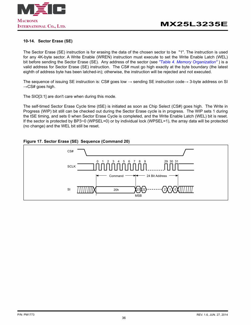
10-14. Sector Erase (SE)
The Sector Erase (SE) instruction is for erasing the data of the chosen sector to be "1". The instruction is used for any 4K-byte sector. A Write Enable (WREN) instruction must execute to set the Write Enable Latch (WEL) bit before sending the Sector Erase (SE). Any address of the sector (see "Table 4. Memory Organization" ) is a valid address for Sector Erase (SE) instruction. The CS# must go high exactly at the byte boundary (the latest eighth of address byte has been latched-in); otherwise, the instruction will be rejected and not executed.
The sequence of issuing SE instruction is: CS# goes low → sending SE instruction code→ 3-byte address on SI →CS# goes high.
The SIO[3:1] are don't care when during this mode.
The self-timed Sector Erase Cycle time (tSE) is initiated as soon as Chip Select (CS#) goes high. The Write in Progress (WIP) bit still can be checked out during the Sector Erase cycle is in progress. The WIP sets 1 during the tSE timing, and sets 0 when Sector Erase Cycle is completed, and the Write Enable Latch (WEL) bit is reset. If the sector is protected by BP3~0 (WPSEL=0) or by individual lock (WPSEL=1), the array data will be protected (no change) and the WEL bit still be reset.
Figure 17. Sector Erase (SE) Sequence (Command 20)
24 Bit Address
21 3 4 5 6 7 8 9 29 30 310
23 22 2 1 0
MSB
SCLK
CS#
SI 20h
Command

37
MX25L3235E
P/N: PM1773 REV. 1.6, JUN. 27, 2014
10-15. Block Erase (BE)
The Block Erase (BE) instruction is for erasing the data of the chosen block to be "1". The instruction is used for 64K-byte block erase operation. A Write Enable (WREN) instruction must execute to set the Write Enable Latch (WEL) bit before sending the Block Erase (BE). Any address of the block (see Table 4. Memory Organization) is a valid address for Block Erase (BE) instruction. The CS# must go high exactly at the byte boundary (the latest eighth of address byte has been latched-in); otherwise, the instruction will be rejected and not executed.
The sequence of issuing BE instruction is: CS# goes low → sending BE instruction code → 3-byte address on SI → CS# goes high.
The SIO[3:1] are don't care when during this mode.
The self-timed Block Erase Cycle time (tBE) is initiated as soon as Chip Select (CS#) goes high. The Write in Progress (WIP) bit still can be checked out during the Sector Erase cycle is in progress. The WIP sets 1 during the tBE timing, and sets 0 when Sector Erase Cycle is completed, and the Write Enable Latch (WEL) bit is reset. If the block is protected by BP3~0 (WPSEL=0) or by individual lock (WPSEL=1), the array data will be protected (no change) and the WEL bit still be reset.
Figure 18. Block Erase (BE) Sequence (Command D8)
24 Bit Address
21 3 4 5 6 7 8 9 29 30 310
23 22 2 01
MSB
SCLK
CS#
SI D8h
Command

38
MX25L3235E
P/N: PM1773 REV. 1.6, JUN. 27, 2014
10-16. Block Erase (BE32K)
The Block Erase (BE32) instruction is for erasing the data of the chosen block to be "1". The instruction is used for 32K-byte block erase operation. A Write Enable (WREN) instruction must execute to set the Write Enable Latch (WEL) bit before sending the Block Erase (BE32). Any address of the block (see "Table 4. Memory Or-ganization" ) is a valid address for Block Erase (BE32) instruction. The CS# must go high exactly at the byte boundary (the latest eighth of address byte has been latched-in); otherwise, the instruction will be rejected and not executed.
The sequence of issuing BE32 instruction is: CS# goes low → sending BE32 instruction code → 3-byte address on SI → CS# goes high.
The SIO[3:1] are don't care when during this mode.
The self-timed Block Erase Cycle time (tBE) is initiated as soon as Chip Select (CS#) goes high. The Write in Progress (WIP) bit still can be checked out during the Sector Erase cycle is in progress. The WIP sets 1 during the tBE timing, and sets 0 when Sector Erase Cycle is completed, and the Write Enable Latch (WEL) bit is reset. If the block is protected by BP3~0 (WPSEL=0) or by individual lock (WPSEL=1), the array data will be protected (no change) and the WEL bit still be reset.
Figure 19. Block Erase 32KB (BE32K) Sequence (Command 52)
24 Bit Address
21 3 4 5 6 7 8 9 29 30 310
23 22 2 01
MSB
SCLK
CS#
SI 52h
Command
39
MX25L3235E
P/N: PM1773 REV. 1.6, JUN. 27, 2014
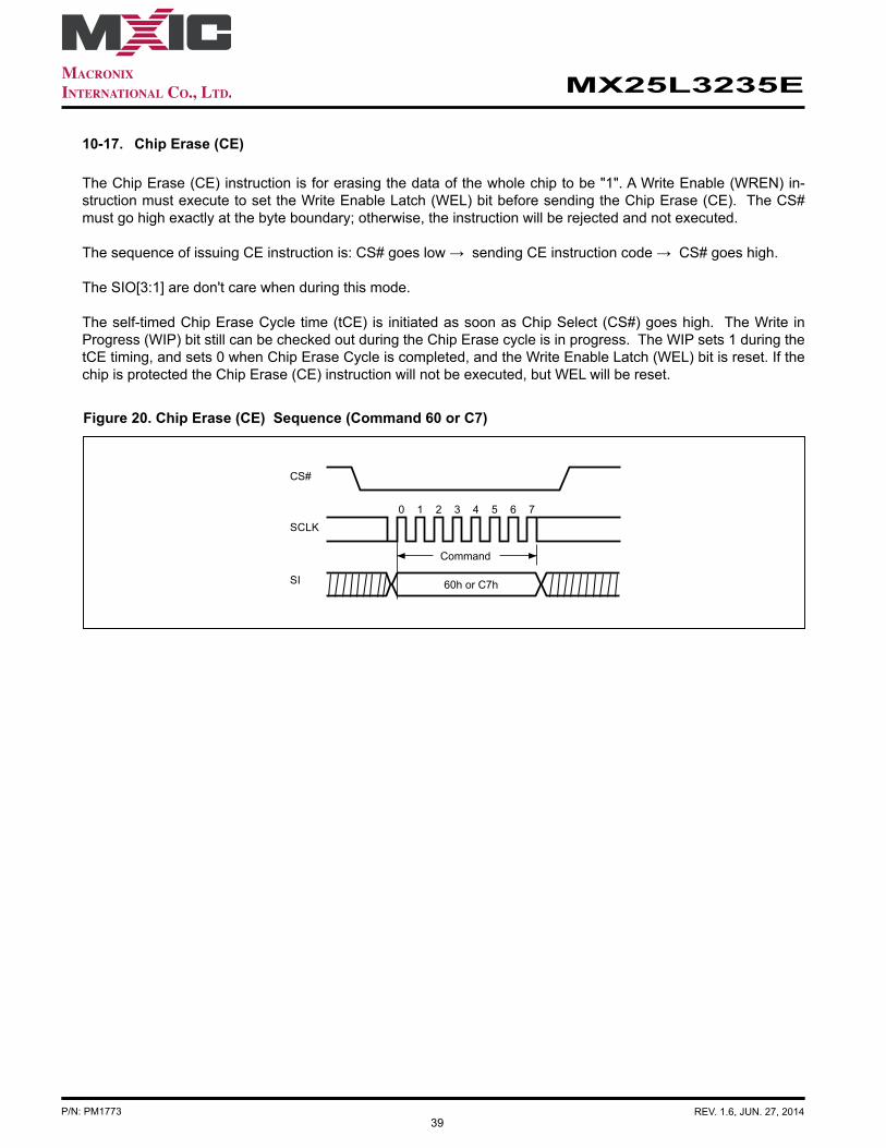
10-17. Chip Erase (CE)
The Chip Erase (CE) instruction is for erasing the data of the whole chip to be "1". A Write Enable (WREN) in-struction must execute to set the Write Enable Latch (WEL) bit before sending the Chip Erase (CE). The CS# must go high exactly at the byte boundary; otherwise, the instruction will be rejected and not executed.
The sequence of issuing CE instruction is: CS# goes low → sending CE instruction code → CS# goes high.
The SIO[3:1] are don't care when during this mode.
The self-timed Chip Erase Cycle time (tCE) is initiated as soon as Chip Select (CS#) goes high. The Write in Progress (WIP) bit still can be checked out during the Chip Erase cycle is in progress. The WIP sets 1 during the tCE timing, and sets 0 when Chip Erase Cycle is completed, and the Write Enable Latch (WEL) bit is reset. If the chip is protected the Chip Erase (CE) instruction will not be executed, but WEL will be reset.
Figure 20. Chip Erase (CE) Sequence (Command 60 or C7)
21 3 4 5 6 70
60h or C7h
SCLK
SI
CS#
Command
40
MX25L3235E
P/N: PM1773 REV. 1.6, JUN. 27, 2014
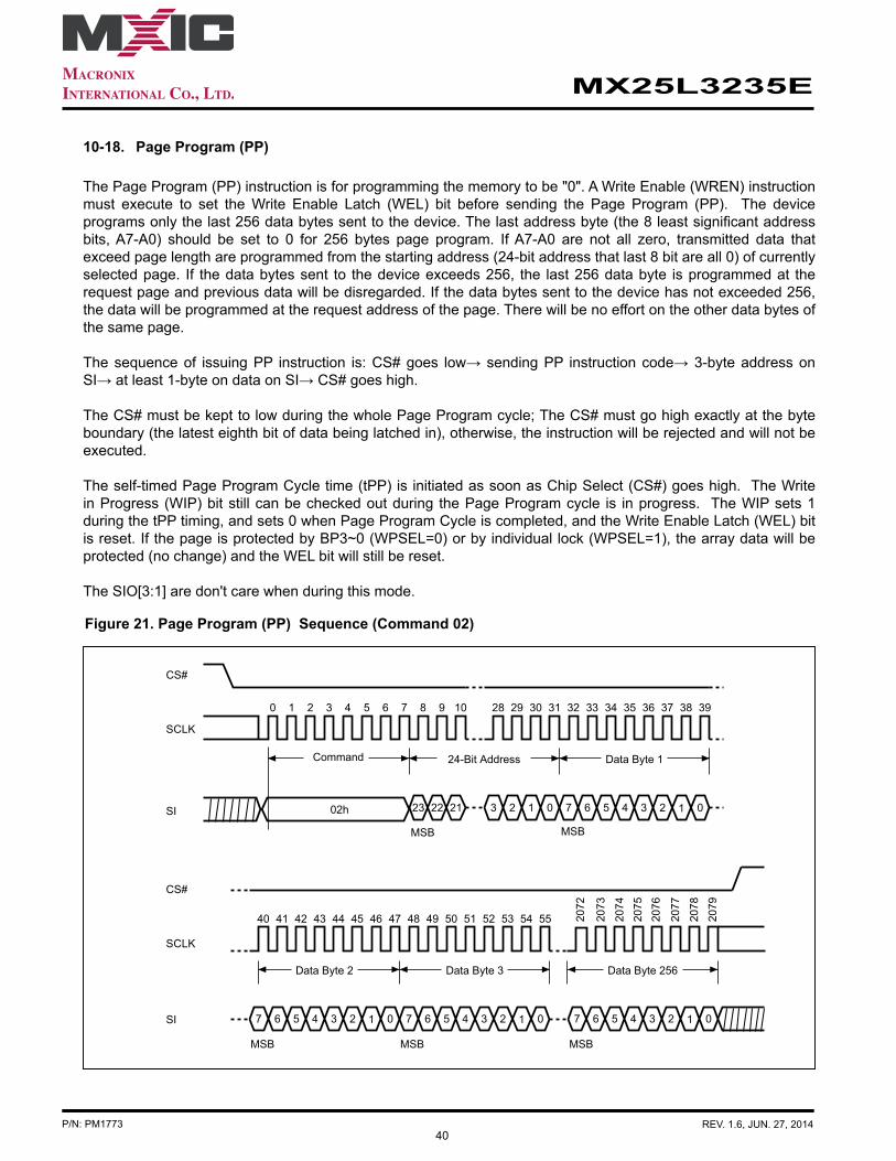
10-18. Page Program (PP)
The Page Program (PP) instruction is for programming the memory to be "0". A Write Enable (WREN) instruction must execute to set the Write Enable Latch (WEL) bit before sending the Page Program (PP). The device programs only the last 256 data bytes sent to the device. The last address byte (the 8 least significant address bits, A7-A0) should be set to 0 for 256 bytes page program. If A7-A0 are not all zero, transmitted data that exceed page length are programmed from the starting address (24-bit address that last 8 bit are all 0) of currently selected page. If the data bytes sent to the device exceeds 256, the last 256 data byte is programmed at the request page and previous data will be disregarded. If the data bytes sent to the device has not exceeded 256, the data will be programmed at the request address of the page. There will be no effort on the other data bytes of the same page.
The sequence of issuing PP instruction is: CS# goes low→ sending PP instruction code→ 3-byte address on SI→ at least 1-byte on data on SI→ CS# goes high.
The CS# must be kept to low during the whole Page Program cycle; The CS# must go high exactly at the byte boundary (the latest eighth bit of data being latched in), otherwise, the instruction will be rejected and will not be executed.
The self-timed Page Program Cycle time (tPP) is initiated as soon as Chip Select (CS#) goes high. The Write in Progress (WIP) bit still can be checked out during the Page Program cycle is in progress. The WIP sets 1 during the tPP timing, and sets 0 when Page Program Cycle is completed, and the Write Enable Latch (WEL) bit is reset. If the page is protected by BP3~0 (WPSEL=0) or by individual lock (WPSEL=1), the array data will be protected (no change) and the WEL bit will still be reset.
The SIO[3:1] are don't care when during this mode.
Figure 21. Page Program (PP) Sequence (Command 02)
4241 43 44 45 46 47 48 49 50 52 53 54 5540
23
21 3 4 5 6 7 8 9 10 28 29 30 31 32 33 34 35
22 21 3 2 1 0
36 37 38
24-Bit Address
0
7 6 5 4 3 2 01
Data Byte 1
39
51
7 6 5 4 3 2 01
Data Byte 2
7 6 5 4 3 2 01
Data Byte 3 Data Byte 256
2079
2078
2077
2076
2075
2074
2073
7 6 5 4 3 2 01
2072
MSB MSB
MSB MSB MSB
SCLK
CS#
SI
SCLK
CS#
SI
02h
Command

41
MX25L3235E
P/N: PM1773 REV. 1.6, JUN. 27, 2014
10-19. 4 x I/O Page Program (4PP)
The Quad Page Program (4PP) instruction is for programming the memory to be "0". A Write Enable (WREN) instruction must execute to set the Write Enable Latch (WEL) bit and Quad Enable (QE) bit must be set to "1" before sending the Quad Page Program (4PP). The Quad Page Programming takes four pins: SIO0, SIO1, SIO2, and SIO3, which can raise programmer performance and the effectiveness of application of lower clock less than 104MHz. For system with faster clock, the Quad page program cannot provide more actual favors, because the required internal page program time is far more than the time data flows in. Therefore, we suggest that while executing this command (especially during sending data), user can slow the clock speed down to 104MHz below. The other function descriptions are as same as standard page program.
The sequence of issuing 4PP instruction is: CS# goes low→ sending 4PP instruction code→ 3-byte address on SIO[3:0]→ at least 1-byte on data on SIO[3:0]→ CS# goes high.
If the page is protected by BP3~0 (WPSEL=0) or by individual lock (WPSEL=1), the array data will be protected (no change) and the WEL bit will still be reset.
Figure 22. 4 x I/O Page Program (4PP) Sequence (Command 38)
A20 A16 A12 A8 A4 A0
A21 A17 A13 A9 A5 A1
A22 A18 A14 A10 A6 A2
A23 A19 A15 A11 A7 A3
21 3 4 5 6 7 8 9
6 ADD cycles DataByte 1
DataByte 2
DataByte 256
0
SCLK
CS#
SI/SIO0
SO/SIO1
HOLD#/SIO3
WP#/SIO2
38
Command
10 11 12 13 14 15 16 17 524 525
…
…
…
…
…
D4 D0
D5 D1
D6 D2
D7 D3
D4 D0
D5 D1
D6 D2
D7 D3
D4 D0
D5 D1
D6 D2
D7 D3
42
MX25L3235E
P/N: PM1773 REV. 1.6, JUN. 27, 2014
The Program/Erase function instruction function flow is as follows:
Figure 23. Program/Erase Flow(1) with read array data
WREN command
Program/erase command
Write program data/address(Write erase address)
RDSR command
Read array data(same address of PGM/ERS)
Program/erase successfully
Yes
YesProgram/erase fail
No
No
Start
Program/erase completed
Verify OK?
WIP=0?
Program/erase another block?
Yes
No
RDSR command*
Yes
WEL=1?No
* * Issue RDSR to check BP[3:0].* If WPSEL=1, issue RDBLOCK to check the block status.

43
MX25L3235E
P/N: PM1773 REV. 1.6, JUN. 27, 2014
Figure 24. Program/Erase Flow(2) without read array data
WREN command
Program/erase command
Write program data/address(Write erase address)
RDSR command
RDSCUR command
Program/erase successfully
Yes
NoProgram/erase fail
YesREGPFAIL/REGEFAIL=1?
WIP=0?
Program/eraseanother block?
Yes
No
RDSR command*
Yes
WEL=1?No
Start
No
Program/erase completed
* Issue RDSR to check BP[3:0].* If WPSEL=1, issue RDBLOCK to check the block status.

44
MX25L3235E
P/N: PM1773 REV. 1.6, JUN. 27, 2014
10-20. Continuous Program mode (CP mode)
The CP mode may enhance program performance by automatically increasing address to the next higher ad-dress after each byte data has been programmed.
The Continuous Program (CP) instruction is for multiple bytes program to Flash. A write Enable (WREN) in-struction must execute to set the Write Enable Latch (WEL) bit before sending the Continuous Program (CP) instruction. CS# requires to go high before CP instruction is executing. After CP instruction and address input, two bytes of data is input sequentially from MSB(bit7) to LSB(bit0). The first byte data will be programmed to the initial address range with A0=0 and second byte data with A0=1. If only one byte data is input, the CP mode will not process. If more than two bytes data are input, the additional data will be ignored and only two byte data are valid. Any byte to be programmed should be in the erase state (FF) first. It will not roll over during the CP mode, once the last unprotected address has been reached, the chip will exit CP mode and reset write Enable Latch bit (WEL) as "0" and CP mode bit as "0". Please check the WIP bit status if it is not in write progress before enter-ing next valid instruction. During CP mode, the valid commands are CP command (AD hex), WRDI command (04 hex), RDSR command (05 hex), and RDSCUR command (2B hex). And the WRDI command is valid after com-pletion of a CP programming cycle, which means the WIP bit=0.
The sequence of issuing CP instruction is : CS# goes low → sending CP instruction code → 3-byte address on SI pin → two data bytes on SI → CS# goes high to low → sending CP instruction and then continue two data bytes are programmed → CS# goes high to low → till last desired two data bytes are programmed → CS# goes high to low →sending WRDI (Write Disable) instruction to end CP mode → send RDSR instruction to verify if CP mode word program ends, or send RDSCUR to check bit4 to verify if CP mode ends.
Three methods to detect the completion of a program cycle during CP mode:
1) Software method-I: by checking WIP bit of Status Register to detect the completion of CP mode.2) Software method-II: by waiting for a tBP time out to determine if it may load next valid command or not.3) Hardware method: by writing ESRY (enable SO to output RY/BY#) instruction to detect the completion of a
program cycle during CP mode. The ESRY instruction must be executed before CP mode execution. Once it is enable in CP mode, the CS# goes low will drive out the RY/BY# status on SO, "0" indicates busy stage, "1" indicates ready stage, SO pin outputs tri-state if CS# goes high. Please note user must send at least one clock cycle on SCLK while CS# is at low to read the status of RY/BY# on SO pin. DSRY (disable SO to output RY/BY#) instruction to disable the SO to output RY/BY# and return to status register data output during CP mode. Please note that the ESRY/DSRY commands are not accepted unless the completion of CP mode.
If the page is protected by BP3~0 (WPSEL=0) or by individual lock (WPSEL=1), the array data will be pro-tected (no change) and the WEL bit will still be reset.

45
MX25L3235E
P/N: PM1773 REV. 1.6, JUN. 27, 2014
Notes: (1) During CP mode, the valid commands are CP command (AD hex), WRDI command (04 hex), RDSR
command (05 hex), RDSCUR command (2B hex), RSTEN command (66 hex) and RST command (99hex). But, RDSR and RDSCUR are invalid commands during CP mode with hardware detection .
(2) Once an internal programming operation begins, CS# goes low will drive the status on the SO pin and CS# goes high will return the SO pin to tri-state. User must send at least one clock cycle on SCLK while CS# is at low to read the status of RY/BY# on SO pin.
(3) To end the CP mode, either reaching the highest unprotected address or sending Write Disable (WRDI) command (04 hex) may achieve it and then it is recommended to send RDSR command (05 hex) to verify if CP mode is ended. Please be noticed that Software reset and Hardware reset can end the CP mode.
CS#
SCLK0 1 6 7 8 9
SI
Command
AD (hex)
30 31 31
S0high impedance
32 47 0
status (2) status (3)
data in24-bit address Byte 0, Byte1
0 1
ValidCommand (1)
data inByte n-1, Byte n
6 7 8 20 21 22 23
04 (hex)
0 0 7 0 7
05 (hex)
8
Figure 25. Continously Program (CP) Mode Sequence with Hardware Detection (Command AD)
46
MX25L3235E
P/N: PM1773 REV. 1.6, JUN. 27, 2014
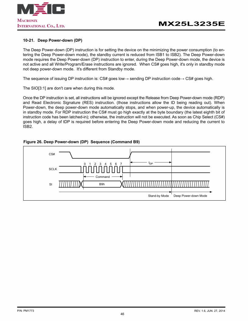
10-21. Deep Power-down (DP)
The Deep Power-down (DP) instruction is for setting the device on the minimizing the power consumption (to en-tering the Deep Power-down mode), the standby current is reduced from ISB1 to ISB2). The Deep Power-down mode requires the Deep Power-down (DP) instruction to enter, during the Deep Power-down mode, the device is not active and all Write/Program/Erase instructions are ignored. When CS# goes high, it's only in standby mode not deep power-down mode. It's different from Standby mode.
The sequence of issuing DP instruction is: CS# goes low→ sending DP instruction code→ CS# goes high.
The SIO[3:1] are don't care when during this mode.
Once the DP instruction is set, all instructions will be ignored except the Release from Deep Power-down mode (RDP) and Read Electronic Signature (RES) instruction. (those instructions allow the ID being reading out). When Power-down, the deep power-down mode automatically stops, and when power-up, the device automatically is in standby mode. For RDP instruction the CS# must go high exactly at the byte boundary (the latest eighth bit of instruction code has been latched-in); otherwise, the instruction will not be executed. As soon as Chip Select (CS#) goes high, a delay of tDP is required before entering the Deep Power-down mode and reducing the current to ISB2.
Figure 26. Deep Power-down (DP) Sequence (Command B9)
21 3 4 5 6 70 tDP
Deep Power-down ModeStand-by Mode
SCLK
CS#
SI B9h
Command
47
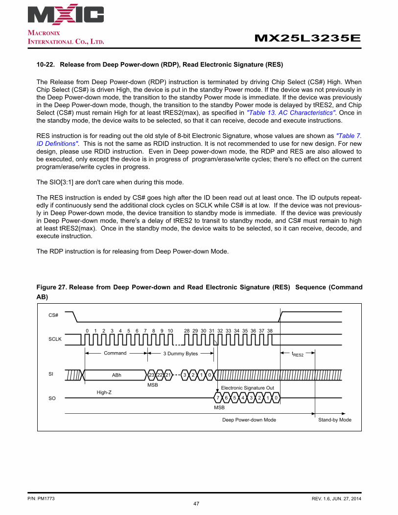
MX25L3235E
P/N: PM1773 REV. 1.6, JUN. 27, 2014
10-22. Release from Deep Power-down (RDP), Read Electronic Signature (RES)
The Release from Deep Power-down (RDP) instruction is terminated by driving Chip Select (CS#) High. When Chip Select (CS#) is driven High, the device is put in the standby Power mode. If the device was not previously in the Deep Power-down mode, the transition to the standby Power mode is immediate. If the device was previously in the Deep Power-down mode, though, the transition to the standby Power mode is delayed by tRES2, and Chip Select (CS#) must remain High for at least tRES2(max), as specified in "Table 13. AC Characteristics". Once in the standby mode, the device waits to be selected, so that it can receive, decode and execute instructions.
RES instruction is for reading out the old style of 8-bit Electronic Signature, whose values are shown as "Table 7. ID Definitions". This is not the same as RDID instruction. It is not recommended to use for new design. For new design, please use RDID instruction. Even in Deep power-down mode, the RDP and RES are also allowed to be executed, only except the device is in progress of program/erase/write cycles; there's no effect on the current program/erase/write cycles in progress.
The SIO[3:1] are don't care when during this mode.
The RES instruction is ended by CS# goes high after the ID been read out at least once. The ID outputs repeat-edly if continuously send the additional clock cycles on SCLK while CS# is at low. If the device was not previous-ly in Deep Power-down mode, the device transition to standby mode is immediate. If the device was previously in Deep Power-down mode, there's a delay of tRES2 to transit to standby mode, and CS# must remain to high at least tRES2(max). Once in the standby mode, the device waits to be selected, so it can receive, decode, and execute instruction.
The RDP instruction is for releasing from Deep Power-down Mode.
Figure 27. Release from Deep Power-down and Read Electronic Signature (RES) Sequence (Command AB)
23
21 3 4 5 6 7 8 9 10 28 29 30 31 32 33 34 35
22 21 3 2 1 0
36 37 38
7 6 5 4 3 2 01High-Z
Electronic Signature Out
3 Dummy Bytes
0
MSB
Stand-by ModeDeep Power-down Mode
MSB
tRES2
SCLK
CS#
SI
SO
ABh
Command
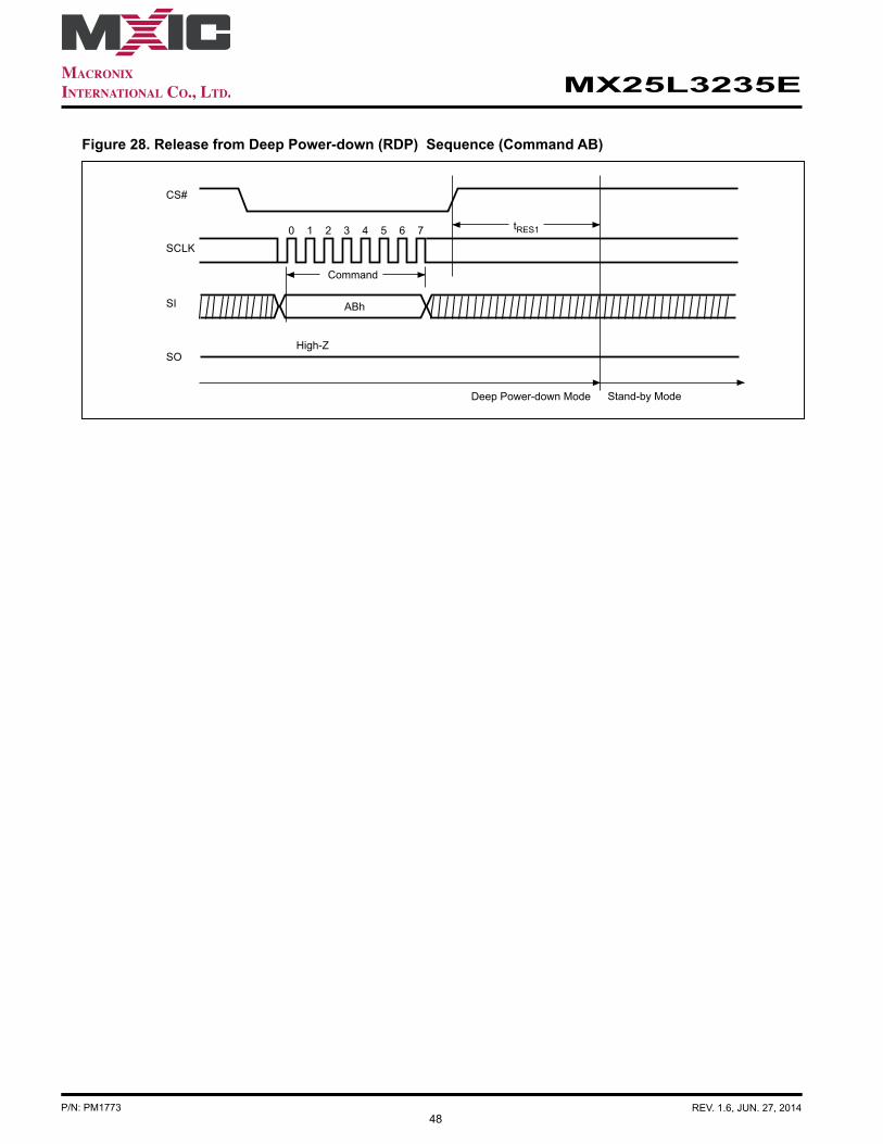
48
MX25L3235E
P/N: PM1773 REV. 1.6, JUN. 27, 2014
21 3 4 5 6 70 tRES1
Stand-by ModeDeep Power-down Mode
High-Z
SCLK
CS#
SI
SO
ABh
Command
Figure 28. Release from Deep Power-down (RDP) Sequence (Command AB)
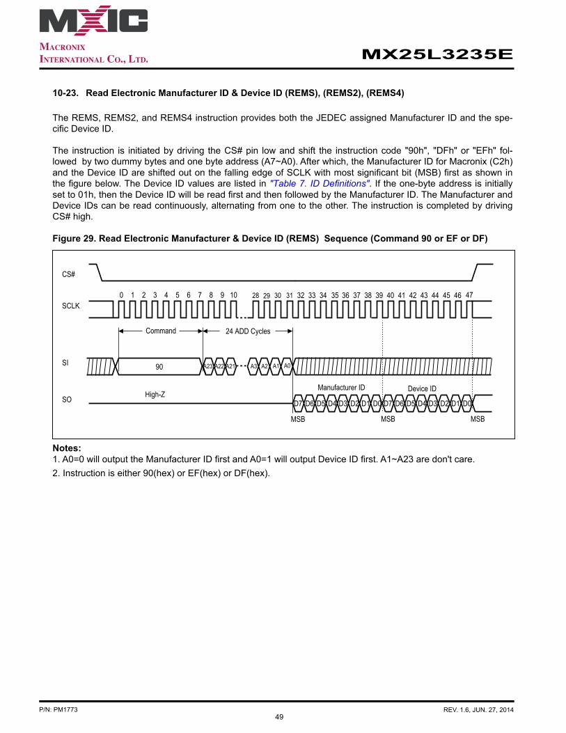
49
MX25L3235E
P/N: PM1773 REV. 1.6, JUN. 27, 2014
10-23. Read Electronic Manufacturer ID & Device ID (REMS), (REMS2), (REMS4)
The REMS, REMS2, and REMS4 instruction provides both the JEDEC assigned Manufacturer ID and the spe-cific Device ID.
The instruction is initiated by driving the CS# pin low and shift the instruction code "90h", "DFh" or "EFh" fol-lowed by two dummy bytes and one byte address (A7~A0). After which, the Manufacturer ID for Macronix (C2h) and the Device ID are shifted out on the falling edge of SCLK with most significant bit (MSB) first as shown in the figure below. The Device ID values are listed in "Table 7. ID Definitions". If the one-byte address is initially set to 01h, then the Device ID will be read first and then followed by the Manufacturer ID. The Manufacturer and Device IDs can be read continuously, alternating from one to the other. The instruction is completed by driving CS# high.
Figure 29. Read Electronic Manufacturer & Device ID (REMS) Sequence (Command 90 or EF or DF)
Notes:1. A0=0 will output the Manufacturer ID first and A0=1 will output Device ID first. A1~A23 are don't care.2. Instruction is either 90(hex) or EF(hex) or DF(hex).
21 3 4 5 6 7 8 9 100 32 33 34 36 37 38 39 40 41 42 43 44 45 46
Manufacturer ID
MSB
Device ID
MSB MSB
4735SCLK
SI
CS#
SO
90
High-Z
Command 24 ADD Cycles
A23 A22 A21 A2A3 A1 A0
D7 D6 D5 D4 D3 D2 D1 D0 D7 D6 D5 D4 D3 D2 D1 D0
313028 29
50
MX25L3235E
P/N: PM1773 REV. 1.6, JUN. 27, 2014
10-24. ID Read
User can execute this ID Read instruction to identify the Device ID and Manufacturer ID. The sequence of issue ID instruction is CS# goes low→sending ID instruction→Data out on SO→CS# goes high. Most significant bit (MSB) first.
After the command cycle, the device will immediately output data on the falling edge of SCLK. The manufacturer ID, memory type, and device ID data byte will be output continuously, until the CS# goes high.
Table 7. ID Definitions Command Type MX25L3235E
RDID manufacturer ID memory type memory densityC2 20 16
RES electronic ID15
REMS/REMS2/REMS4
manufacturer ID device IDC2 15
10-25. Enter Secured OTP (ENSO)
The ENSO instruction is for entering the additional 4K-bit Secured OTP mode. The additional 4K-bit Secured OTP is independent from main array, which may use to store unique serial number for system identifier. After entering the Secured OTP mode, and then follow standard read or program procedure to read out the data or update data. The Secured OTP data cannot be updated again once it is lock-down.
The sequence of issuing ENSO instruction is: CS# goes low→ sending ENSO instruction to enter Secured OTP mode→ CS# goes high.
The SIO[3:1] are don't care when during this mode.
Please note that WRSR/WRSCUR/WPSEL/SBLK/GBLK/SBULK/GBULK/CE/BE/SE/BE32K commands are not acceptable during the access of secure OTP region, once Security OTP is locked down, only read related com-mands are valid.
10-26. Exit Secured OTP (EXSO)
The EXSO instruction is for exiting the additional 4K-bit Secured OTP mode.The sequence of issuing EXSO instruction is: CS# goes low→ sending EXSO instruction to exit Secured OTP mode→ CS# goes high.
The SIO[3:1] are don't care when during this mode.
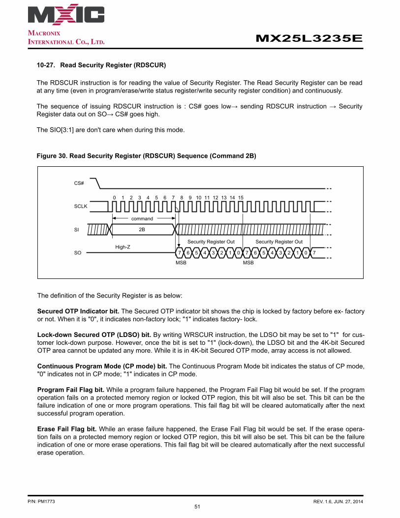
51
MX25L3235E
P/N: PM1773 REV. 1.6, JUN. 27, 2014
10-27. Read Security Register (RDSCUR)
The RDSCUR instruction is for reading the value of Security Register. The Read Security Register can be read at any time (even in program/erase/write status register/write security register condition) and continuously.
The sequence of issuing RDSCUR instruction is : CS# goes low→ sending RDSCUR instruction → Security Register data out on SO→ CS# goes high.
The SIO[3:1] are don't care when during this mode.
21 3 4 5 6 7 8 9 10 11 12 13 14 15
command
0
7 6 5 4 3 2 1 0
Security Register Out Security Register OutHigh-Z
MSB
7 6 5 4 3 2 1 0
MSB
7
SCLK
SI
CS#
SO
2B
Figure 30. Read Security Register (RDSCUR) Sequence (Command 2B)
The definition of the Security Register is as below:
Secured OTP Indicator bit. The Secured OTP indicator bit shows the chip is locked by factory before ex- factory or not. When it is "0", it indicates non-factory lock; "1" indicates factory- lock.
Lock-down Secured OTP (LDSO) bit. By writing WRSCUR instruction, the LDSO bit may be set to "1" for cus-tomer lock-down purpose. However, once the bit is set to "1" (lock-down), the LDSO bit and the 4K-bit Secured OTP area cannot be updated any more. While it is in 4K-bit Secured OTP mode, array access is not allowed.
Continuous Program Mode (CP mode) bit. The Continuous Program Mode bit indicates the status of CP mode, "0" indicates not in CP mode; "1" indicates in CP mode.
Program Fail Flag bit. While a program failure happened, the Program Fail Flag bit would be set. If the program operation fails on a protected memory region or locked OTP region, this bit will also be set. This bit can be the failure indication of one or more program operations. This fail flag bit will be cleared automatically after the next successful program operation.
Erase Fail Flag bit. While an erase failure happened, the Erase Fail Flag bit would be set. If the erase opera-tion fails on a protected memory region or locked OTP region, this bit will also be set. This bit can be the failure indication of one or more erase operations. This fail flag bit will be cleared automatically after the next successful erase operation.
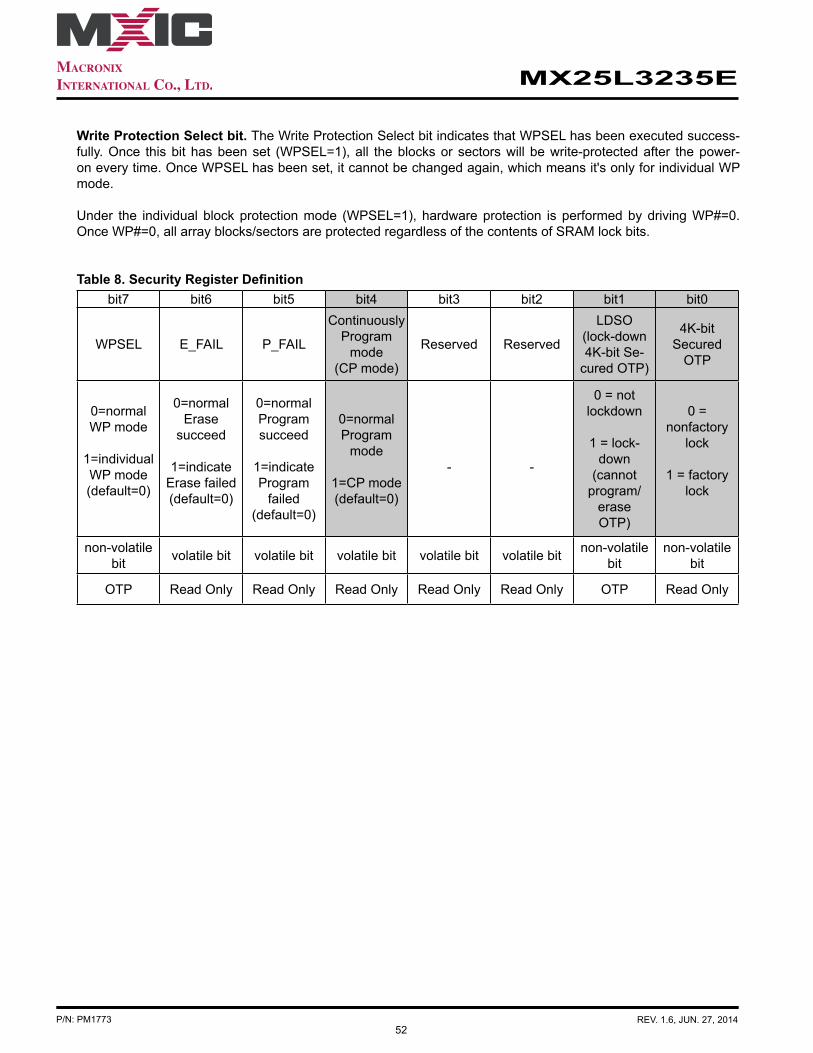
52
MX25L3235E
P/N: PM1773 REV. 1.6, JUN. 27, 2014
Write Protection Select bit. The Write Protection Select bit indicates that WPSEL has been executed success-fully. Once this bit has been set (WPSEL=1), all the blocks or sectors will be write-protected after the power-on every time. Once WPSEL has been set, it cannot be changed again, which means it's only for individual WP mode.
Under the individual block protection mode (WPSEL=1), hardware protection is performed by driving WP#=0. Once WP#=0, all array blocks/sectors are protected regardless of the contents of SRAM lock bits.
Table 8. Security Register Definitionbit7 bit6 bit5 bit4 bit3 bit2 bit1 bit0
WPSEL E_FAIL P_FAIL
ContinuouslyProgram
mode(CP mode)
Reserved Reserved
LDSO(lock-down 4K-bit Se-
cured OTP)
4K-bit Secured
OTP
0=normalWP mode
1=individualWP mode(default=0)
0=normalErase
succeed
1=indicateErase failed(default=0)
0=normalProgram succeed
1=indicateProgram
failed(default=0)
0=normalProgram
mode
1=CP mode(default=0)
- -
0 = not lockdown
1 = lock-down
(cannotprogram/
eraseOTP)
0 = nonfactory
lock
1 = factorylock
non-volatile bit volatile bit volatile bit volatile bit volatile bit volatile bit non-volatile
bitnon-volatile
bit
OTP Read Only Read Only Read Only Read Only Read Only OTP Read Only
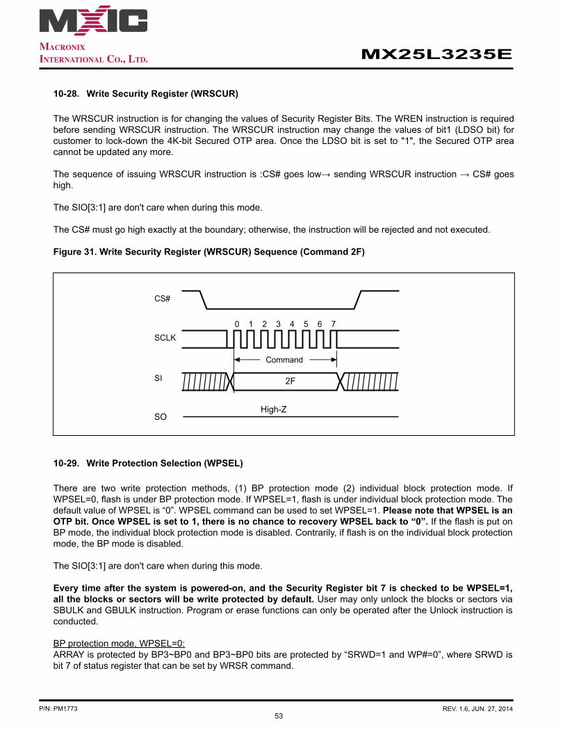
53
MX25L3235E
P/N: PM1773 REV. 1.6, JUN. 27, 2014
10-28. Write Security Register (WRSCUR)
The WRSCUR instruction is for changing the values of Security Register Bits. The WREN instruction is required before sending WRSCUR instruction. The WRSCUR instruction may change the values of bit1 (LDSO bit) for customer to lock-down the 4K-bit Secured OTP area. Once the LDSO bit is set to "1", the Secured OTP area cannot be updated any more.
The sequence of issuing WRSCUR instruction is :CS# goes low→ sending WRSCUR instruction → CS# goes high.
The SIO[3:1] are don't care when during this mode.
The CS# must go high exactly at the boundary; otherwise, the instruction will be rejected and not executed.
Figure 31. Write Security Register (WRSCUR) Sequence (Command 2F)
21 3 4 5 6 70
2F
SCLK
SI
CS#
Command
SOHigh-Z
10-29. Write Protection Selection (WPSEL)
There are two write protection methods, (1) BP protection mode (2) individual block protection mode. If WPSEL=0, flash is under BP protection mode. If WPSEL=1, flash is under individual block protection mode. The default value of WPSEL is “0”. WPSEL command can be used to set WPSEL=1. Please note that WPSEL is an OTP bit. Once WPSEL is set to 1, there is no chance to recovery WPSEL back to “0”. If the flash is put on BP mode, the individual block protection mode is disabled. Contrarily, if flash is on the individual block protection mode, the BP mode is disabled.
The SIO[3:1] are don't care when during this mode.
Every time after the system is powered-on, and the Security Register bit 7 is checked to be WPSEL=1, all the blocks or sectors will be write protected by default. User may only unlock the blocks or sectors via SBULK and GBULK instruction. Program or erase functions can only be operated after the Unlock instruction is conducted.
BP protection mode, WPSEL=0:ARRAY is protected by BP3~BP0 and BP3~BP0 bits are protected by “SRWD=1 and WP#=0”, where SRWD is bit 7 of status register that can be set by WRSR command.

54
MX25L3235E
P/N: PM1773 REV. 1.6, JUN. 27, 2014
21 3 4 5 6 70
68
SCLK
SI
CS#
Command
Individual block protection mode, WPSEL=1:Blocks are individually protected by their own SRAM lock bits which are set to “1” after power up. SBULK and SBLK command can set SRAM lock bit to “0” and “1”. When the system accepts and executes WPSEL instruc-tion, the bit 7 in security register will be set. It will activate SBLK, SBULK, RDBLOCK, GBLK, GBULK, PBLK, RDPBLK etc instructions to conduct block lock protection and replace the original Software Protect Mode (SPM) use (BP3~BP0) indicated block methods. Under the individual block protection mode (WPSEL=1), hardware protection is performed by driving WP#=0. Once WP#=0, all array blocks/sectors are protected regardless of the contents of SRAM lock bits.
The WREN (Write Enable) instruction is required before issuing WPSEL instruction.The sequence of issuing WPSEL instruction is: CS# goes low → sending WPSEL instruction to enter the indi-vidual block protect mode → CS# goes high.
Figure 32. Write Protection Selection (WPSEL) Sequence (Command 68)
WPSEL instruction function flow is as follows:
Figure 33. BP and SRWD if WPSEL=0
64KB
64KB
.
.
.
64KB
64KB
BP3 BP2 BP1 BP0 SRWD
WPB pin
(1) BP3~BP0 is used to define the protection group region. (The protected area size see "Table 2. Protected Area Sizes" )
(2) “SRWD=1 and WPB=0” is used to protect BP3~BP0. In this case, SRWD and BP3~BP0 of status register bits can not be changed by WRSR

55
MX25L3235E
P/N: PM1773 REV. 1.6, JUN. 27, 2014
Figure 34. The individual block lock mode is effective after setting WPSEL=1
64KB
4KB
64KB
4KB
SRAM
SRAMSRAM
4KB
4KB
SRAM
Uniform64KB blocks
SRAM
SRAM
4KB SRAM
SBULK / SBLK / GBULK / GBLK / RDBLOCK
……
…… …
………
Bottom4KBx16Sectors
TOP 4KBx16Sectors
• Power-Up: All SRAM bits=1 (all blocks are default protected). All arrays cannot be programmed/erased
• SBLK/SBULK(36h/39h): - SBLK(36h) : Set SRAM bit=1 (protect) : array can not be
programmed /erased - SBULK(39h): Set SRAM bit=0 (unprotect): array can be
programmed /erased - All top 4KBx16 sectors and bottom 4KBx16 sectors
and other 64KB uniform blocks can be protected and unprotected SRAM bits individually by SBLK/SBULK command set.
• GBLK/ GBULK(7Eh/98h): - GBLK(7Eh):Set all SRAM bits=1,whole chip are protected
and cannot be programmed / erased. - GBULK(98h):Set all SRAM bits=0,whole chip are
unprotected and can be programmed / erased. - All sectors and blocks SRAM bits of whole chip can be
protected and unprotected at one time by GBLK/GBULK command set.
• RDBLOCK(3Ch): - use RDBLOCK mode to check the SRAM bits status after
SBULK /SBLK/GBULK/GBLK command set.

56
MX25L3235E
P/N: PM1773 REV. 1.6, JUN. 27, 2014
Figure 35. WPSEL Flow
RDSCUR(2Bh) command
RDSR command
RDSCUR(2Bh) command
WPSEL set successfully
Yes
Yes
WPSEL set fail
No
start
WPSEL=1?
WIP=0?No
WPSEL disable,block protected by BP[3:0]
Yes
No
WPSEL=1?
WPSEL(68h) command
WPSEL enable.Block protected by individual lock
(SBLK, SBULK, … etc).

57
MX25L3235E
P/N: PM1773 REV. 1.6, JUN. 27, 2014
10-30. Single Block Lock/Unlock Protection (SBLK/SBULK)
These instructions are only effective after WPSEL was executed. The SBLK instruction is for write protection a specified block(or sector) of memory, using A23-A16 or (A23-A12) address bits to assign a 64Kbytes block (or 4K bytes sector) to be protected as read only. The SBULK instruction will cancel the block (or sector) write pro-tection state. This feature allows user to stop protecting the entire block (or sector) through the chip unprotect command (GBULK).
The WREN (Write Enable) instruction is required before issuing SBLK/SBULK instruction.The sequence of issuing SBLK/SBULK instruction is: CS# goes low → send SBLK/SBULK (36h/39h) instruction → send 3 address bytes assign one block (or sector) to be protected on SI pin → CS# goes high.
The CS# must go high exactly at the byte boundary, otherwise the instruction will be rejected and not be execut-ed.
The SIO[3:1] are don't care when during this mode.
Figure 36. Single Block Lock/Unlock Protection (SBLK/SBULK) Sequence (Command 36/39)
24 Bit AddressCycles
21 3 4 5 6 7 8 9 29 30 310
MSB
SCLK
CS#
SI 36/39
Command
A23 A22 A2 A1 A0

58
MX25L3235E
P/N: PM1773 REV. 1.6, JUN. 27, 2014
SBLK/SBULK instruction function flow is as follows:
Figure 37. Block Lock Flow
RDSCUR(2Bh) command
Start
WREN command
SBLK command( 36h + 24bit address )
RDSR command
RDBLOCK command( 3Ch + 24bit address )
Block lock successfully
Yes
Yes
Block lock fail
NoData = FFh ?
WIP=0?
Lock another block?
Block lock completed
No
Yes
No
No
Yes
WPSEL=1? WPSEL command
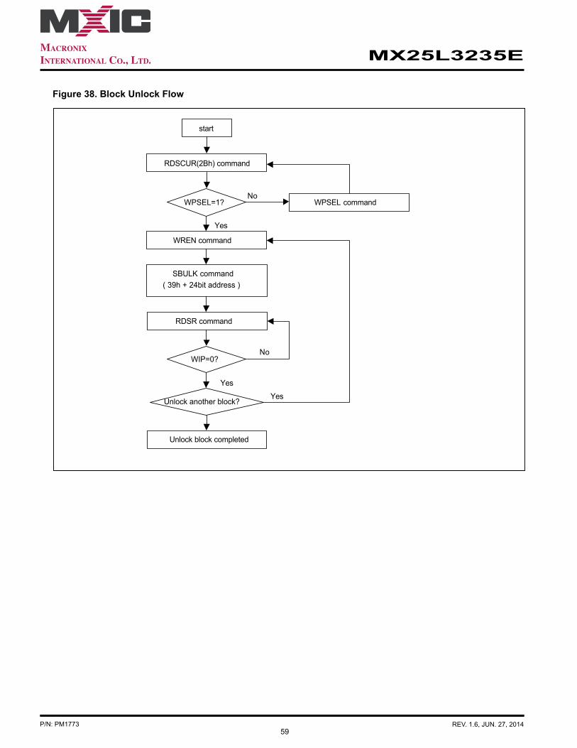
59
MX25L3235E
P/N: PM1773 REV. 1.6, JUN. 27, 2014
Figure 38. Block Unlock Flow
WREN command
RDSCUR(2Bh) command
SBULK command( 39h + 24bit address )
RDSR command
Yes
WIP=0?
Unlock another block?Yes
No
No
Yes
Unlock block completed
start
WPSEL=1? WPSEL command

60
MX25L3235E
P/N: PM1773 REV. 1.6, JUN. 27, 2014
10-31. Read Block Lock Status (RDBLOCK)
This instruction is only effective after WPSEL was executed. The RDBLOCK instruction is for reading the status of protection lock of a specified block(or sector), using A23-A16 (or A23-A12) address bits to assign a 64K bytes block (4K bytes sector) and read protection lock status bit which the first byte of Read-out cycle. The status bit is"1" to indicate that this block has been protected, that user can read only but cannot write/program /erase this block. The status bit is "0" to indicate that this block hasn't be protected, and user can read and write this block.
The sequence of issuing RDBLOCK instruction is: CS# goes low → send RDBLOCK (3Ch) instruction → send 3 address bytes to assign one block on SI pin → read block's protection lock status bit on SO pin → CS# goes high.
The SIO[3:1] are don't care when during this mode.
Figure 39. Read Block Protection Lock Status (RDBLOCK) Sequence (Command 3C)
21 3 4 5 6 7 8 9 10 28 29 30 31 32 33 34 35 36 37 38
High-ZBlock Protection Lock status out
24 ADD Cycles
0
MSB
MSB
SCLK
CS#
SI
SO
3C
Command
A23 A22 A21 A3 A2 A1 A0
D7 D6 D5 D4 D3 D2 D1 D0
39
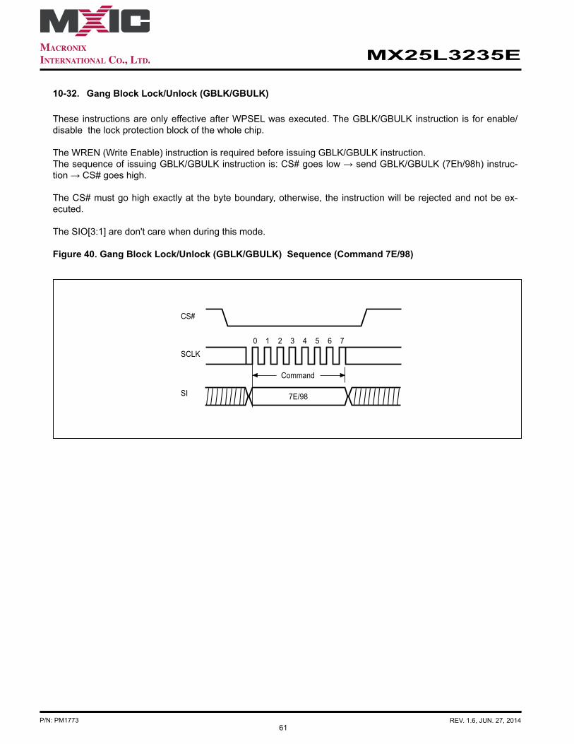
61
MX25L3235E
P/N: PM1773 REV. 1.6, JUN. 27, 2014
10-32. Gang Block Lock/Unlock (GBLK/GBULK)
These instructions are only effective after WPSEL was executed. The GBLK/GBULK instruction is for enable/disable the lock protection block of the whole chip.
The WREN (Write Enable) instruction is required before issuing GBLK/GBULK instruction.The sequence of issuing GBLK/GBULK instruction is: CS# goes low → send GBLK/GBULK (7Eh/98h) instruc-tion → CS# goes high.
The CS# must go high exactly at the byte boundary, otherwise, the instruction will be rejected and not be ex-ecuted.
The SIO[3:1] are don't care when during this mode.
Figure 40. Gang Block Lock/Unlock (GBLK/GBULK) Sequence (Command 7E/98)
21 3 4 5 6 70
7E/98
SCLK
SI
CS#
Command
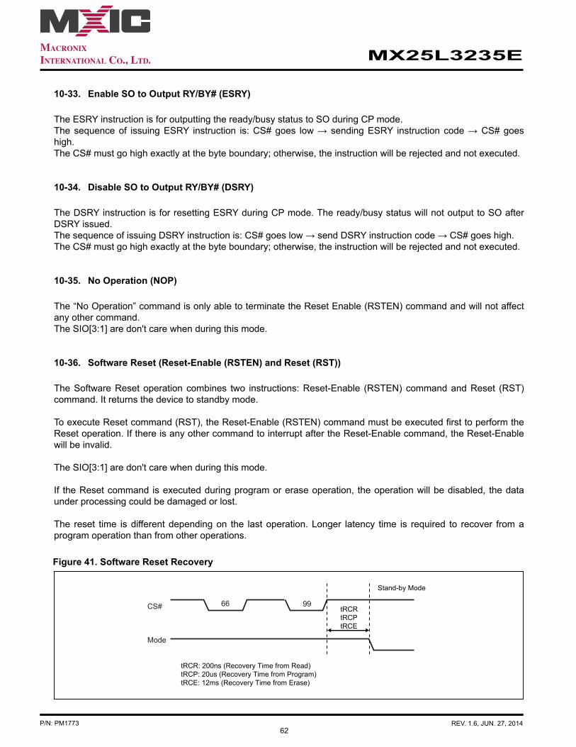
62
MX25L3235E
P/N: PM1773 REV. 1.6, JUN. 27, 2014
10-33. Enable SO to Output RY/BY# (ESRY)
The ESRY instruction is for outputting the ready/busy status to SO during CP mode. The sequence of issuing ESRY instruction is: CS# goes low → sending ESRY instruction code → CS# goes high. The CS# must go high exactly at the byte boundary; otherwise, the instruction will be rejected and not executed.
10-34. Disable SO to Output RY/BY# (DSRY)
The DSRY instruction is for resetting ESRY during CP mode. The ready/busy status will not output to SO after DSRY issued.The sequence of issuing DSRY instruction is: CS# goes low → send DSRY instruction code → CS# goes high. The CS# must go high exactly at the byte boundary; otherwise, the instruction will be rejected and not executed.
10-35. No Operation (NOP)
The “No Operation” command is only able to terminate the Reset Enable (RSTEN) command and will not affect any other command.The SIO[3:1] are don't care when during this mode.
10-36. Software Reset (Reset-Enable (RSTEN) and Reset (RST))
The Software Reset operation combines two instructions: Reset-Enable (RSTEN) command and Reset (RST) command. It returns the device to standby mode.
To execute Reset command (RST), the Reset-Enable (RSTEN) command must be executed first to perform the Reset operation. If there is any other command to interrupt after the Reset-Enable command, the Reset-Enable will be invalid.
The SIO[3:1] are don't care when during this mode.
If the Reset command is executed during program or erase operation, the operation will be disabled, the data under processing could be damaged or lost.
The reset time is different depending on the last operation. Longer latency time is required to recover from a program operation than from other operations.
Figure 41. Software Reset Recovery
CS#
Mode
66 99
Stand-by Mode
tRCRtRCPtRCE
tRCR: 200ns (Recovery Time from Read)tRCP: 20us (Recovery Time from Program)tRCE: 12ms (Recovery Time from Erase)

63
MX25L3235E
P/N: PM1773 REV. 1.6, JUN. 27, 2014
10-37. Read SFDP Mode (RDSFDP)
The Serial Flash Discoverable Parameter (SFDP) standard provides a consistent method of describing the functional and feature capabilities of serial flash devices in a standard set of internal parameter tables. These parameter tables can be interrogated by host system software to enable adjustments needed to accommodate divergent features from multiple vendors. The concept is similar to the one found in the Introduction of JEDEC Standard, JESD68 on CFI.
The sequence of issuing RDSFDP instruction is CS# goes low→send RDSFDP instruction (5Ah)→send 3 address bytes on SI pin→send 1 dummy byte on SI pin→read SFDP code on SO→to end RDSFDP operation can use CS# to high at any time during data out.
SFDP is a JEDEC Standard, JESD216.
Figure 42. Read Serial Flash Discoverable Parameter (RDSFDP) Sequence
23
21 3 4 5 6 7 8 9 10 28 29 30 31
22 21 3 2 1 0
High-Z
24 BIT ADDRESS
0
32 33 34 36 37 38 39 40 41 42 43 44 45 46
7 6 5 4 3 2 01
DATA OUT 1
Dummy Cycle
MSB
7 6 5 4 3 2 1 0
DATA OUT 2
MSB MSB
7
47
7 6 5 4 3 2 01
35
SCLK
SI
CS#
SO
SCLK
SI
CS#
SO
5Ah
Command
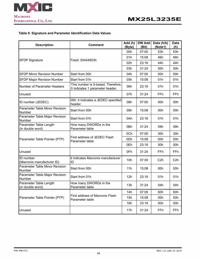
64
MX25L3235E
P/N: PM1773 REV. 1.6, JUN. 27, 2014
Table 9. Signature and Parameter Identification Data Values
Description Comment Add (h)(Byte)
DW Add (Bit)
Data (h/b) (Note1)
Data(h)
SFDP Signature Fixed: 50444653h
00h 07:00 53h 53h
01h 15:08 46h 46h
02h 23:16 44h 44h
03h 31:24 50h 50h
SFDP Minor Revision Number Start from 00h 04h 07:00 00h 00h
SFDP Major Revision Number Start from 01h 05h 15:08 01h 01h
Number of Parameter Headers This number is 0-based. Therefore, 0 indicates 1 parameter header. 06h 23:16 01h 01h
Unused 07h 31:24 FFh FFh
ID number (JEDEC) 00h: it indicates a JEDEC specified header. 08h 07:00 00h 00h
Parameter Table Minor Revision Number Start from 00h 09h 15:08 00h 00h
Parameter Table Major Revision Number Start from 01h 0Ah 23:16 01h 01h
Parameter Table Length (in double word)
How many DWORDs in the Parameter table 0Bh 31:24 09h 09h
Parameter Table Pointer (PTP) First address of JEDEC Flash Parameter table
0Ch 07:00 30h 30h
0Dh 15:08 00h 00h
0Eh 23:16 00h 00h
Unused 0Fh 31:24 FFh FFh
ID number (Macronix manufacturer ID)
it indicates Macronix manufacturer ID 10h 07:00 C2h C2h
Parameter Table Minor Revision Number Start from 00h 11h 15:08 00h 00h
Parameter Table Major Revision Number Start from 01h 12h 23:16 01h 01h
Parameter Table Length (in double word)
How many DWORDs in the Parameter table 13h 31:24 04h 04h
Parameter Table Pointer (PTP) First address of Macronix Flash Parameter table
14h 07:00 60h 60h
15h 15:08 00h 00h
16h 23:16 00h 00h
Unused 17h 31:24 FFh FFh
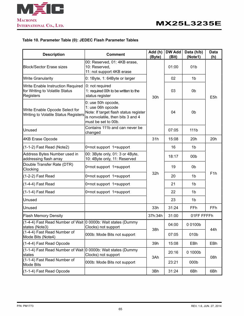
65
MX25L3235E
P/N: PM1773 REV. 1.6, JUN. 27, 2014
Table 10. Parameter Table (0): JEDEC Flash Parameter Tables
Description Comment Add (h)(Byte)
DW Add (Bit)
Data (h/b) (Note1)
Data(h)
Block/Sector Erase sizes00: Reserved, 01: 4KB erase, 10: Reserved, 11: not support 4KB erase
30h
01:00 01b
E5h
Write Granularity 0: 1Byte, 1: 64Byte or larger 02 1b
Write Enable Instruction Required for Writing to Volatile Status Registers
0: not required1: required 00h to be written to the status register
03 0b
Write Enable Opcode Select for Writing to Volatile Status Registers
0: use 50h opcode, 1: use 06h opcode Note: If target flash status register is nonvolatile, then bits 3 and 4 must be set to 00b.
04 0b
Unused Contains 111b and can never be changed 07:05 111b
4KB Erase Opcode 31h 15:08 20h 20h
(1-1-2) Fast Read (Note2) 0=not support 1=support
32h
16 1b
F1h
Address Bytes Number used in addressing flash array
00: 3Byte only, 01: 3 or 4Byte, 10: 4Byte only, 11: Reserved 18:17 00b
Double Transfer Rate (DTR) Clocking 0=not support 1=support 19 0b
(1-2-2) Fast Read 0=not support 1=support 20 1b
(1-4-4) Fast Read 0=not support 1=support 21 1b
(1-1-4) Fast Read 0=not support 1=support 22 1b
Unused 23 1b
Unused 33h 31:24 FFh FFh
Flash Memory Density 37h:34h 31:00 01FF FFFFh(1-4-4) Fast Read Number of Wait states (Note3)
0 0000b: Wait states (Dummy Clocks) not support 38h
04:00 0 0100b44h(1-4-4) Fast Read Number of
Mode Bits (Note4) 000b: Mode Bits not support 07:05 010b
(1-4-4) Fast Read Opcode 39h 15:08 EBh EBh(1-1-4) Fast Read Number of Wait states
0 0000b: Wait states (Dummy Clocks) not support 3Ah
20:16 0 1000b08h(1-1-4) Fast Read Number of
Mode Bits 000b: Mode Bits not support 23:21 000b
(1-1-4) Fast Read Opcode 3Bh 31:24 6Bh 6Bh
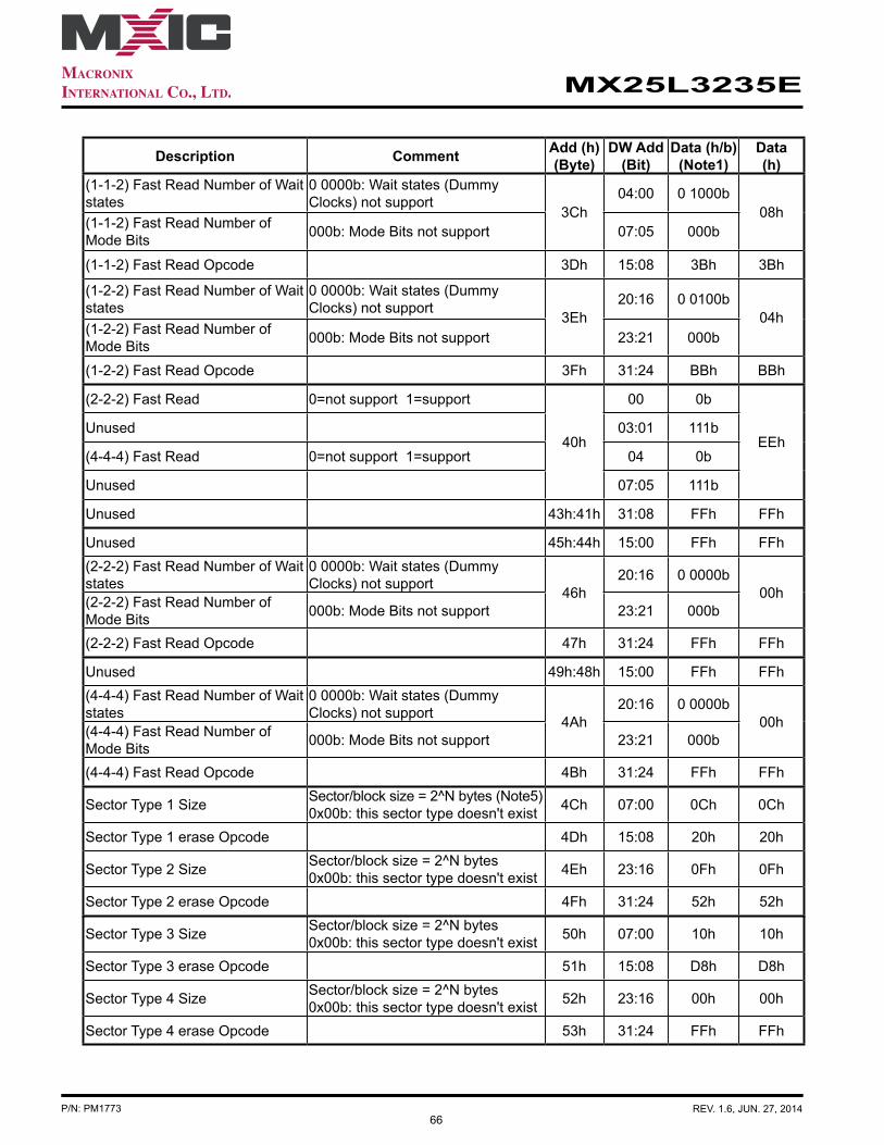
66
MX25L3235E
P/N: PM1773 REV. 1.6, JUN. 27, 2014
Description Comment Add (h)(Byte)
DW Add (Bit)
Data (h/b) (Note1)
Data(h)
(1-1-2) Fast Read Number of Wait states
0 0000b: Wait states (Dummy Clocks) not support
3Ch04:00 0 1000b
08h(1-1-2) Fast Read Number of Mode Bits 000b: Mode Bits not support 07:05 000b
(1-1-2) Fast Read Opcode 3Dh 15:08 3Bh 3Bh
(1-2-2) Fast Read Number of Wait states
0 0000b: Wait states (Dummy Clocks) not support
3Eh20:16 0 0100b
04h(1-2-2) Fast Read Number of Mode Bits 000b: Mode Bits not support 23:21 000b
(1-2-2) Fast Read Opcode 3Fh 31:24 BBh BBh
(2-2-2) Fast Read 0=not support 1=support
40h
00 0b
EEhUnused 03:01 111b
(4-4-4) Fast Read 0=not support 1=support 04 0b
Unused 07:05 111b
Unused 43h:41h 31:08 FFh FFh
Unused 45h:44h 15:00 FFh FFh(2-2-2) Fast Read Number of Wait states
0 0000b: Wait states (Dummy Clocks) not support 46h
20:16 0 0000b00h(2-2-2) Fast Read Number of
Mode Bits 000b: Mode Bits not support 23:21 000b
(2-2-2) Fast Read Opcode 47h 31:24 FFh FFh
Unused 49h:48h 15:00 FFh FFh(4-4-4) Fast Read Number of Wait states
0 0000b: Wait states (Dummy Clocks) not support 4Ah
20:16 0 0000b00h(4-4-4) Fast Read Number of
Mode Bits 000b: Mode Bits not support 23:21 000b
(4-4-4) Fast Read Opcode 4Bh 31:24 FFh FFh
Sector Type 1 Size Sector/block size = 2^N bytes (Note5) 0x00b: this sector type doesn't exist 4Ch 07:00 0Ch 0Ch
Sector Type 1 erase Opcode 4Dh 15:08 20h 20h
Sector Type 2 Size Sector/block size = 2^N bytes 0x00b: this sector type doesn't exist 4Eh 23:16 0Fh 0Fh
Sector Type 2 erase Opcode 4Fh 31:24 52h 52h
Sector Type 3 Size Sector/block size = 2^N bytes 0x00b: this sector type doesn't exist 50h 07:00 10h 10h
Sector Type 3 erase Opcode 51h 15:08 D8h D8h
Sector Type 4 Size Sector/block size = 2^N bytes 0x00b: this sector type doesn't exist 52h 23:16 00h 00h
Sector Type 4 erase Opcode 53h 31:24 FFh FFh

67
MX25L3235E
P/N: PM1773 REV. 1.6, JUN. 27, 2014
Table 11. Parameter Table (1): Macronix Flash Parameter Tables
Description Comment Add (h)(Byte)
DW Add (Bit)
Data (h/b) (Note1)
Data (h)
Vcc Supply Maximum Voltage2000h=2.000V 2700h=2.700V 3600h=3.600V
61h:60h 07:0015:08
00h 36h
00h 36h
Vcc Supply Minimum Voltage
1650h=1.650V 2250h=2.250V 2350h=2.350V 2700h=2.700V
63h:62h 23:1631:24
00h 27h
00h 27h
H/W Reset# pin 0=not support 1=support
65h:64h
00 0b
499Eh
H/W Hold# pin 0=not support 1=support 01 1b
Deep Power Down Mode 0=not support 1=support 02 1b
S/W Reset 0=not support 1=support 03 1b
S/W Reset Opcode Reset Enable (66h) should be issued before Reset Opcode 11:04 1001 1001b
(99h)
Program Suspend/Resume 0=not support 1=support 12 0b
Erase Suspend/Resume 0=not support 1=support 13 0b
Unused 14 1b
Wrap-Around Read mode 0=not support 1=support 15 0b
Wrap-Around Read mode Opcode 66h 23:16 FFh FFh
Wrap-Around Read data length
08h:support 8B wrap-around read 16h:8B&16B 32h:8B&16B&32B 64h:8B&16B&32B&64B
67h 31:24 FFh FFh
Individual block lock 0=not support 1=support
6Bh:68h
00 1b
C8D9h
Individual block lock bit(Volatile/Nonvolatile) 0=Volatile 1=Nonvolatile 01 0b
Individual block lock Opcode 09:02 0011 0110b (36h)
Individual block lock Volatile protect bit default protect status 0=protect 1=unprotect 10 0b
Secured OTP 0=not support 1=support 11 1b
Read Lock 0=not support 1=support 12 0b
Permanent Lock 0=not support 1=support 13 0b
Unused 15:14 11b
Unused 31:16 FFh FFh
Unused 6Fh:6Ch 31:00 FFh FFh

68
MX25L3235E
P/N: PM1773 REV. 1.6, JUN. 27, 2014
Note 1: h/b is hexadecimal or binary.Note 2: (x-y-z) means I/O mode nomenclature used to indicate the number of active pins used for the opcode (x),
address (y), and data (z). At the present time, the only valid Read SFDP instruction modes are: (1-1-1), (2-2-2), and (4-4-4)
Note 3: Wait States is required dummy clock cycles after the address bits or optional mode bits.Note 4: Mode Bits is optional control bits that follow the address bits. These bits are driven by the system
controller if they are specified. (eg,read performance enhance toggling bits)Note 5: 4KB=2^0Ch,32KB=2^0Fh,64KB=2^10hNote 6: All unused and undefined area data is blank FFh.

69
MX25L3235E
P/N: PM1773 REV. 1.6, JUN. 27, 2014
11. POWER-ON STATE
The device is at below states when power-up: - Standby mode (please note it is not Deep Power-down mode) - Write Enable Latch (WEL) bit is reset
The device must not be selected during power-up and power-down stage unless the VCC achieves below cor-rect level: - VCC minimum at power-up stage and then after a delay of tVSL - GND at power-downPlease note that a pull-up resistor on CS# may ensure a safe and proper power-up/down level.
An internal Power-on Reset (POR) circuit may protect the device from data corruption and inadvertent data change during power up state.
For further protection on the device, if the VCC does not reach the VCC minimum level, the correct operation is not guaranteed. The read, write, erase, and program command should be sent after the time delay: - tVSL after VCC reached VCC minimum levelThe device can accept read command after VCC reached VCC minimum and a time delay of tVSL.
Note:- To stabilize the VCC level, the VCC rail decoupled by a suitable capacitor close to package pins is recommend-ed. (generally around 0.1uF)
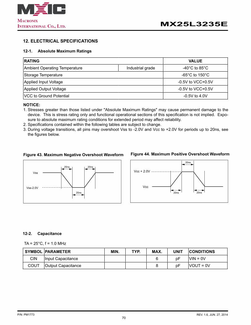
70
MX25L3235E
P/N: PM1773 REV. 1.6, JUN. 27, 2014
Vss
Vss-2.0V
20ns 20ns
20ns
Vcc + 2.0V
Vcc
20ns 20ns
20ns
12. ELECTRICAL SPECIFICATIONS
12-1. Absolute Maximum Ratings
SYMBOL PARAMETER MIN. TYP. MAX. UNIT CONDITIONSCIN Input Capacitance 6 pF VIN = 0V
COUT Output Capacitance 8 pF VOUT = 0V
RATING VALUEAmbient Operating Temperature Industrial grade -40°C to 85°C
Storage Temperature -65°C to 150°C
Applied Input Voltage -0.5V to VCC+0.5V
Applied Output Voltage -0.5V to VCC+0.5V
VCC to Ground Potential -0.5V to 4.0V
NOTICE:1. Stresses greater than those listed under "Absolute Maximum Ratings" may cause permanent damage to the
device. This is stress rating only and functional operational sections of this specification is not implied. Expo-sure to absolute maximum rating conditions for extended period may affect reliability.
2. Specifications contained within the following tables are subject to change.3. During voltage transitions, all pins may overshoot Vss to -2.0V and Vcc to +2.0V for periods up to 20ns, see
the figures below.
Figure 43. Maximum Negative Overshoot Waveform
12-2. Capacitance
Figure 44. Maximum Positive Overshoot Waveform
TA = 25°C, f = 1.0 MHz
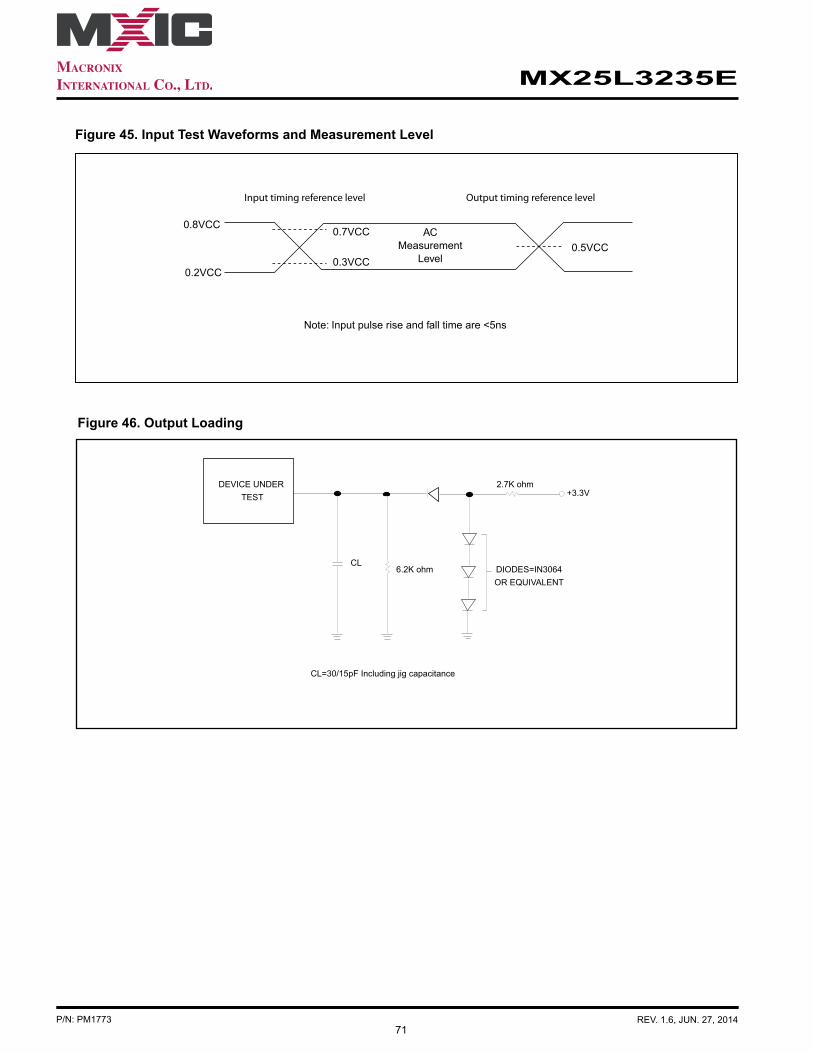
71
MX25L3235E
P/N: PM1773 REV. 1.6, JUN. 27, 2014
DEVICE UNDER TEST
DIODES=IN3064OR EQUIVALENT
CL6.2K ohm
2.7K ohm+3.3V
CL=30/15pF Including jig capacitance
Figure 45. Input Test Waveforms and Measurement Level
Figure 46. Output Loading
ACMeasurement
Level
Input timing reference level Output timing reference level
0.8VCC0.7VCC
0.3VCC0.5VCC
0.2VCC
Note: Input pulse rise and fall time are <5ns

72
MX25L3235E
P/N: PM1773 REV. 1.6, JUN. 27, 2014
Table 12. DC Characteristics
Notes :1. Typical values at VCC = 3.3V, T = 25°C. These currents are valid for all product versions (package and
speeds).2. Typical value is calculated by simulation.3. The value guaranteed by characterization, not 100% tested in production.
Symbol Parameter Notes Min. Typ. Max. Units Test Conditions
ILI Input Load Current 1 ± 2 uA VCC = VCC Max, VIN = VCC or GND
ILO Output Leakage Current 1 ± 2 uA VCC = VCC Max, VOUT = VCC or GND
ISB1 VCC Standby Current 1 15 50 uA VIN = VCC or GND, CS# = VCC
ISB2 Deep Power-down Current 1 25 uA VIN = VCC or GND, CS# = VCC
ICC1 VCC Read 1
35 mAf=104MHz (4 x I/O read) SCLK=0.1VCC/0.9VCC, SO=Open
19 mAf=104MHz (1 x I/O read) SCLK=0.1VCC/0.9VCC, SO=Open
25 mAfQ=86MHz (4 x I/O read) SCLK=0.1VCC/0.9VCC, SO=Open
20 mAfT=86MHz (2 x I/O read)SCLK=0.1VCC/0.9VCC, SO=Open
10 mAf=33MHz, SCLK=0.1VCC/0.9VCC, SO=Open
ICC2 VCC Program Current (PP) 1 15 25 mA Program in Progress, CS# =
VCC
ICC3VCC Write Status Register (WRSR) Current
15 20 mA Program status register in progress, CS#=VCC
ICC4 VCC Sector Erase Current (SE) 1 10 25 mA Erase in Progress, CS#=VCC
ICC5 VCC Chip Erase Current (CE) 1 15 25 mA Erase in Progress, CS#=VCC
VIL Input Low Voltage -0.5 0.8 V
VIH Input High Voltage 0.7VCC VCC+0.4 V
VOL Output Low Voltage 0.4 V IOL = 1.6mA
VOH Output High Voltage VCC-0.2 V IOH = -100uA
Temperature = -40°C to 85°C for Industrial grade

73
MX25L3235E
P/N: PM1773 REV. 1.6, JUN. 27, 2014
Table 13. AC Characteristics
Symbol Alt. Parameter Min. Typ. Max. Unit
fSCLK fC Clock Frequency for all commands (except READ, 2READ, DREAD, 4READ, QREAD, 4PP instructions) D.C. 104 MHz
fRSCLK fR Clock Frequency for READ instructions 50 MHz
fTSCLK fT Clock Frequency for 2READ/DREAD instructions 86 MHzfQ Clock Frequency for 4READ/QREAD instructions (4) 86 MHz
tCH(1) tCLH Clock High Time Others (fSCLK) 4.5 nsNormal Read (fRSCLK) 9 ns
tCL(1) tCLL Clock Low Time Others (fSCLK) 4.5 nsNormal Read (fRSCLK) 9 ns
tCLCH Clock Rise Time (3) (peak to peak) 0.1 V/nstCHCL Clock Fall Time (3) (peak to peak) 0.1 V/nstSLCH tCSS CS# Active Setup Time (relative to SCLK) 4 nstCHSL CS# Not Active Hold Time (relative to SCLK) 4 nstDVCH tDSU Data In Setup Time 2 nstCHDX tDH Data In Hold Time 3 nstCHSH CS# Active Hold Time (relative to SCLK) 4 nstSHCH CS# Not Active Setup Time (relative to SCLK) 4 ns
tSHSL(3) tCSH CS# Deselect Time Read 15 nsWrite/Erase/Program 50 ns
tSHQZ tDIS Output Disable Time 2.7V-3.6V 10 ns3.0V-3.6V 8 ns
tHLCH HOLD# Active Setup Time (relative to SCLK) 5 nstCHHH HOLD# Active Hold Time (relative to SCLK) 5 nstHHCH HOLD# Not Active Setup Time (relative to SCLK) 5 nstCHHL HOLD# Not Active Hold Time (relative to SCLK) 5 ns
tHHQX tLZ HOLD# to Output Low-Z Loading=30pF
2.7V-3.6V 10 ns3.0V-3.6V 8 ns
tHLQZ tHZ HOLD# to Output High-Z Loading=30pF
2.7V-3.6V 10 ns3.0V-3.6V 8 ns
tCLQV tV Clock Low to Output Valid VCC=2.7V~3.6V
Loading: 10pF
1 I/O 5 ns2 I/O & 4 I/O 6 ns
Loading: 15pF
1 I/O 6 ns2 I/O & 4 I/O 6 ns
Loading: 30pF
1 I/O 7 ns2 I/O & 4 I/O 8 ns
tCLQX tHO Output Hold Time 1 nstWHSL Write Protect Setup Time 20 nstSHWL Write Protect Hold Time 100 ns
tDP CS# High to Deep Power-down Mode 10 us
tRES1 CS# High to Standby Mode without Electronic Signature Read 100 us
tRES2 CS# High to Standby Mode with Electronic Signature Read 100 us
Temperature = -40°C to 85°C for Industrial grade
74
MX25L3235E
P/N: PM1773 REV. 1.6, JUN. 27, 2014
Notes: 1. tCH + tCL must be greater than or equal to 1/ fC. 2. The value guaranteed by characterization, not 100% tested in production.3. Only applicable as a constraint for a WRSR instruction when SRWD is set at 1.4. For 4READ instruction, when dummy cycle=6, clock rate is 86MHz (default), and when dummy cycle=8, clock
rate is 104MHz.
Symbol Alt. Parameter Min. Typ. Max. UnittW Write Status Register Cycle Time 40 mstBP Byte-Program 12 50 ustPP Page Program Cycle Time 0.7 3 mstSE Sector Erase Cycle Time (4KB) 30 200 mstBE Block Erase Cycle Time (32KB) 0.14 1.6 stBE Block Erase Cycle Time (64KB) 0.25 2 stCE Chip Erase Cycle Time 10 50 s
tWPS Write Protection Selection Time 1 mstWSR Write Security Register Time 1 ms
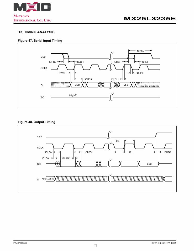
75
MX25L3235E
P/N: PM1773 REV. 1.6, JUN. 27, 2014
Figure 47. Serial Input Timing
Figure 48. Output Timing
13. TIMING ANALYSIS
SCLK
SI
CS#
MSB
SO
tDVCH
High-Z
LSB
tSLCH
tCHDX
tCHCL
tCLCH
tSHCH
tSHSL
tCHSHtCHSL
LSB
ADDR.LSB IN
tSHQZ
tCH
tCL
tCLQX
tCLQV
tCLQX
tCLQV
SCLK
SO
CS#
SI
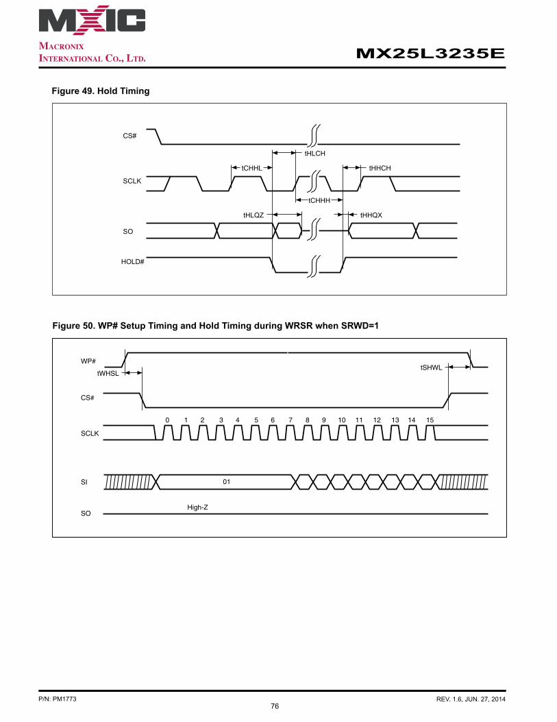
76
MX25L3235E
P/N: PM1773 REV. 1.6, JUN. 27, 2014
Figure 49. Hold Timing
High-Z
01
0 1 2 3 4 5 6 7 8 9 10 11 12 13 14 15
tWHSLtSHWL
SCLK
SI
CS#
WP#
SO
Figure 50. WP# Setup Timing and Hold Timing during WRSR when SRWD=1
tCHHL
tHLCH
tHHCH
tCHHH
tHHQXtHLQZ
SCLK
SO
CS#
HOLD#
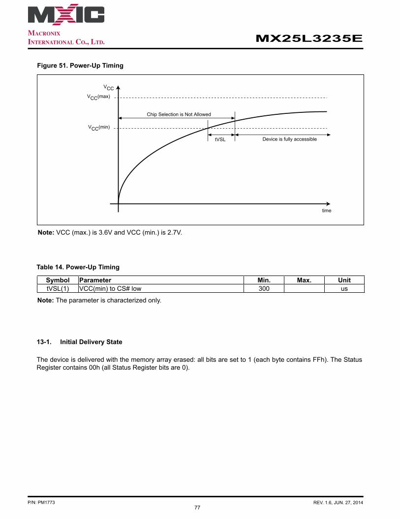
77
MX25L3235E
P/N: PM1773 REV. 1.6, JUN. 27, 2014
13-1. Initial Delivery State
The device is delivered with the memory array erased: all bits are set to 1 (each byte contains FFh). The Status Register contains 00h (all Status Register bits are 0).
Note: The parameter is characterized only.
Symbol Parameter Min. Max. UnittVSL(1) VCC(min) to CS# low 300 us
Note: VCC (max.) is 3.6V and VCC (min.) is 2.7V.
VCC
VCC(min)
Chip Selection is Not Allowed
tVSL
time
Device is fully accessible
VCC(max)
Table 14. Power-Up Timing
Figure 51. Power-Up Timing

78
MX25L3235E
P/N: PM1773 REV. 1.6, JUN. 27, 2014
Notes :1. Sampled, not 100% tested.2. For AC spec tCHSL, tSLCH, tDVCH, tCHDX, tSHSL, tCHSH, tSHCH, tCHCL, tCLCH in the figure, please refer
to "Table 13. AC Characteristics".
Symbol Parameter Notes Min. Max. UnittVR VCC Rise Time 1 20 500000 us/V
14. OPERATING CONDITIONS
At Device Power-Up and Power-Down
AC timing illustrated in "Figure 52. AC Timing at Device Power-Up" and "Figure 53. Power-Down Sequence" are for the supply voltages and the control signals at device power-up and power-down. If the timing in the figures is ignored, the device will not operate correctly.
During power-up and power-down, CS# needs to follow the voltage applied on VCC to keep the device not to be selected. The CS# can be driven low when VCC reach Vcc(min.) and wait a period of tVSL.
Figure 52. AC Timing at Device Power-Up
SCLK
SI
CS#
VCC
MSB IN
SO
tDVCH
High Impedance
LSB IN
tSLCH
tCHDX
tCHCL
tCLCH
tSHCH
tSHSL
tCHSHtCHSL
tVR
VCC(min)
GND
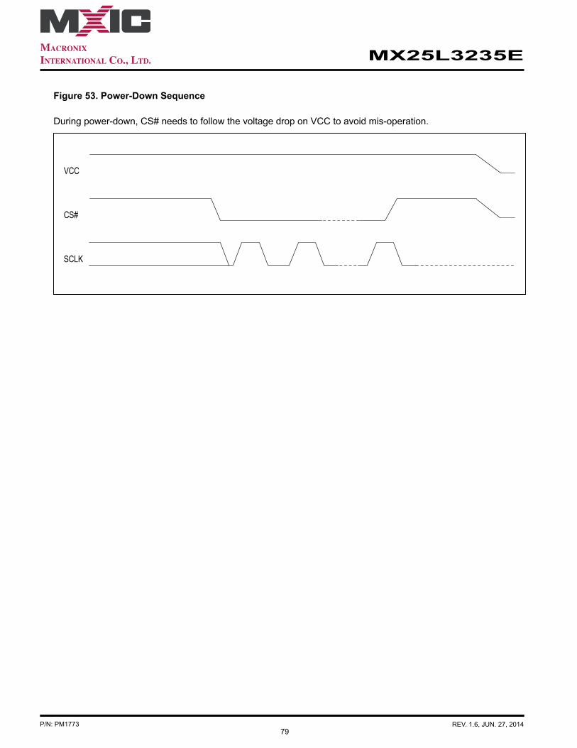
79
MX25L3235E
P/N: PM1773 REV. 1.6, JUN. 27, 2014
Figure 53. Power-Down Sequence
CS#
SCLK
VCC
During power-down, CS# needs to follow the voltage drop on VCC to avoid mis-operation.
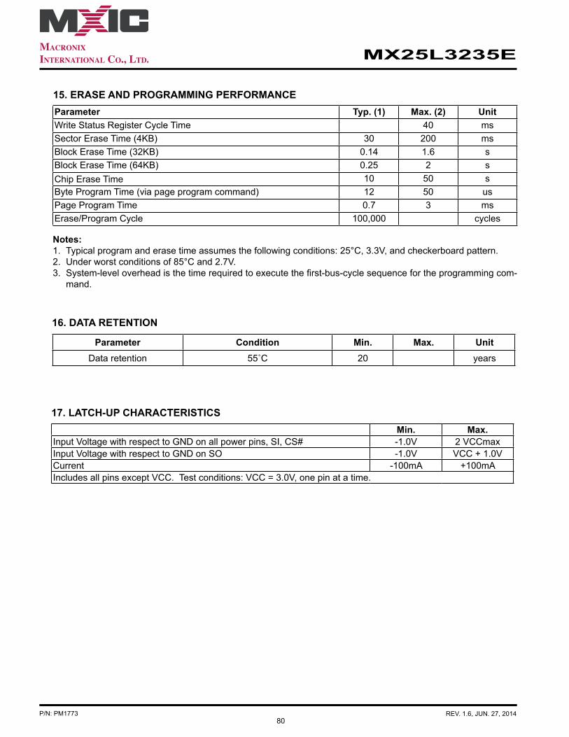
80
MX25L3235E
P/N: PM1773 REV. 1.6, JUN. 27, 2014
15. ERASE AND PROGRAMMING PERFORMANCE
Notes: 1. Typical program and erase time assumes the following conditions: 25°C, 3.3V, and checkerboard pattern.2. Under worst conditions of 85°C and 2.7V.3. System-level overhead is the time required to execute the first-bus-cycle sequence for the programming com-
mand.
16. DATA RETENTION
Min. Max.Input Voltage with respect to GND on all power pins, SI, CS# -1.0V 2 VCCmaxInput Voltage with respect to GND on SO -1.0V VCC + 1.0VCurrent -100mA +100mAIncludes all pins except VCC. Test conditions: VCC = 3.0V, one pin at a time.
Parameter Typ. (1) Max. (2) UnitWrite Status Register Cycle Time 40 msSector Erase Time (4KB) 30 200 msBlock Erase Time (32KB) 0.14 1.6 sBlock Erase Time (64KB) 0.25 2 sChip Erase Time 10 50 sByte Program Time (via page program command) 12 50 usPage Program Time 0.7 3 msErase/Program Cycle 100,000 cycles
17. LATCH-UP CHARACTERISTICS
Parameter Condition Min. Max. UnitData retention 55˚C 20 years

81
MX25L3235E
P/N: PM1773 REV. 1.6, JUN. 27, 2014
18. ORDERING INFORMATION
PART NO. CLOCK (MHz) TEMPERATURE PACKAGE Remark
MX25L3235EMI-10G 104 -40°C~85°C 16-SOP(300mil)
MX25L3235EM2I-10G 104 -40°C~85°C 8-SOP(200mil)
MX25L3235EZNI-10G 104 -40°C~85°C 8-WSON(6x5mm)
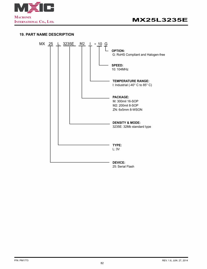
82
MX25L3235E
P/N: PM1773 REV. 1.6, JUN. 27, 2014
19. PART NAME DESCRIPTION
MX 25 L M2 I
TEMPERATURE RANGE:I: Industrial (-40° C to 85° C)
PACKAGE:M: 300mil 16-SOPM2: 200mil 8-SOPZN: 6x5mm 8-WSON
DENSITY & MODE:3235E: 32Mb standard type
TYPE:L: 3V
DEVICE:25: Serial Flash
3235E 10 G
OPTION:G: RoHS Compliant and Halogen-free
SPEED:10: 104MHz
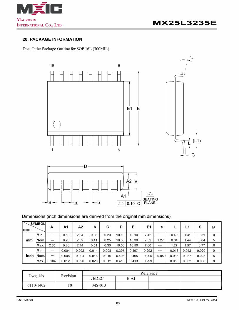
83
MX25L3235E
P/N: PM1773 REV. 1.6, JUN. 27, 2014
20. PACKAGE INFORMATION
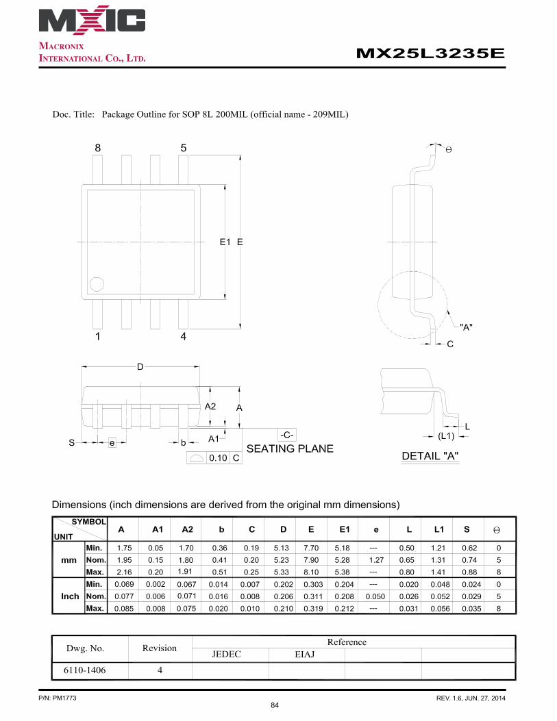
84
MX25L3235E
P/N: PM1773 REV. 1.6, JUN. 27, 2014
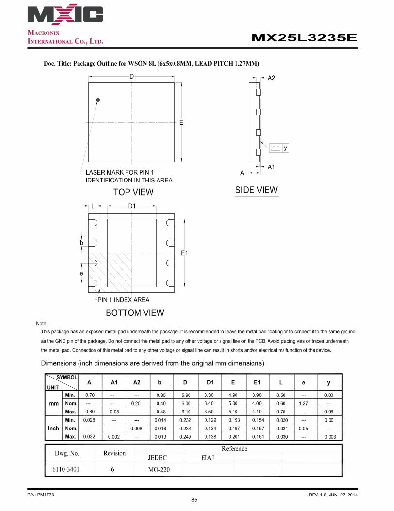
85
MX25L3235E
P/N: PM1773 REV. 1.6, JUN. 27, 2014
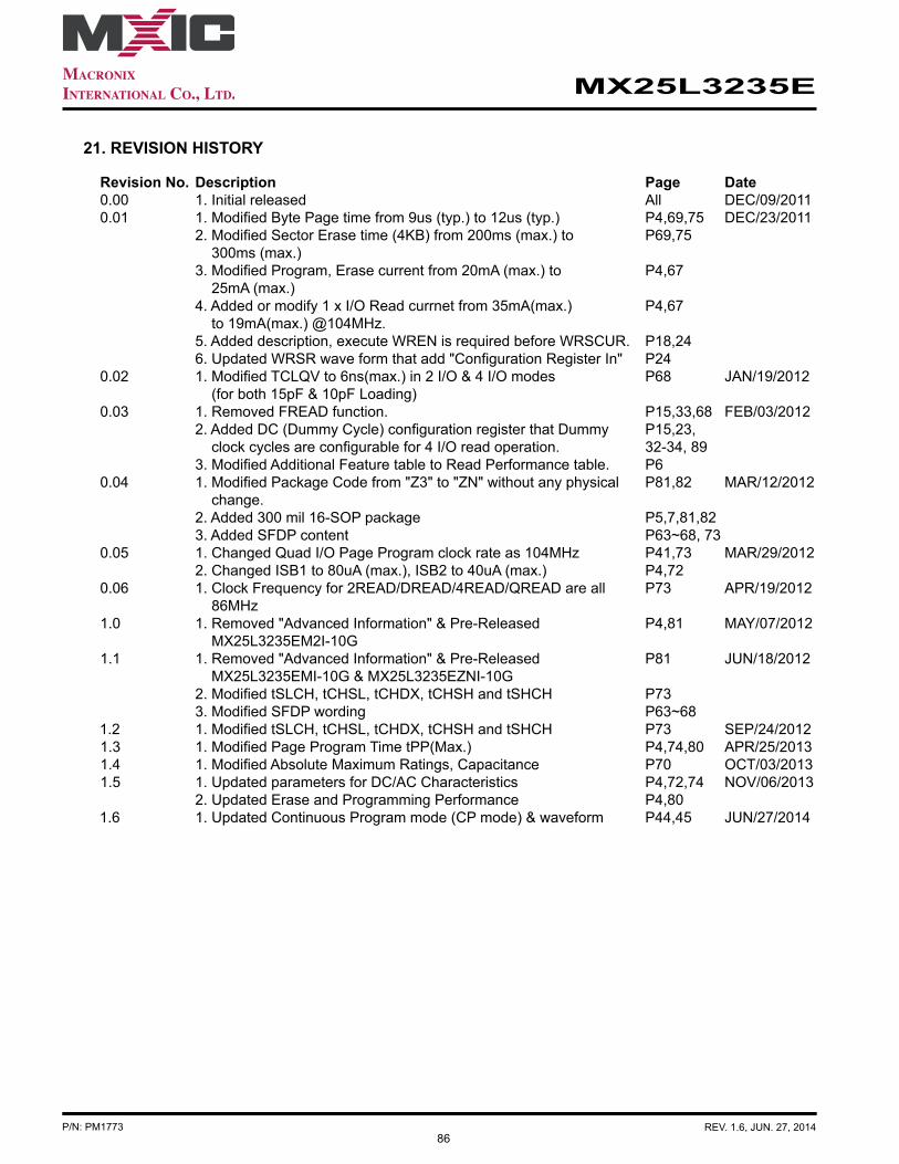
86
MX25L3235E
P/N: PM1773 REV. 1.6, JUN. 27, 2014
21. REVISION HISTORY
Revision No. Description Page Date0.00 1. Initial released All DEC/09/20110.01 1. Modified Byte Page time from 9us (typ.) to 12us (typ.) P4,69,75 DEC/23/2011 2. Modified Sector Erase time (4KB) from 200ms (max.) to P69,75 300ms (max.) 3. Modified Program, Erase current from 20mA (max.) to P4,67 25mA (max.) 4. Added or modify 1 x I/O Read currnet from 35mA(max.) P4,67 to 19mA(max.) @104MHz. 5. Added description, execute WREN is required before WRSCUR. P18,24 6. Updated WRSR wave form that add "Configuration Register In" P24 0.02 1. Modified TCLQV to 6ns(max.) in 2 I/O & 4 I/O modes P68 JAN/19/2012 (for both 15pF & 10pF Loading) 0.03 1. Removed FREAD function. P15,33,68 FEB/03/2012 2. Added DC (Dummy Cycle) configuration register that Dummy P15,23, clock cycles are configurable for 4 I/O read operation. 32-34, 89 3. Modified Additional Feature table to Read Performance table. P60.04 1. Modified Package Code from "Z3" to "ZN" without any physical P81,82 MAR/12/2012 change. 2. Added 300 mil 16-SOP package P5,7,81,82 3. Added SFDP content P63~68, 730.05 1. Changed Quad I/O Page Program clock rate as 104MHz P41,73 MAR/29/2012 2. Changed ISB1 to 80uA (max.), ISB2 to 40uA (max.) P4,720.06 1. Clock Frequency for 2READ/DREAD/4READ/QREAD are all P73 APR/19/2012 86MHz1.0 1. Removed "Advanced Information" & Pre-Released P4,81 MAY/07/2012 MX25L3235EM2I-10G1.1 1. Removed "Advanced Information" & Pre-Released P81 JUN/18/2012 MX25L3235EMI-10G & MX25L3235EZNI-10G 2. Modified tSLCH, tCHSL, tCHDX, tCHSH and tSHCH P73 3. Modified SFDP wording P63~681.2 1. Modified tSLCH, tCHSL, tCHDX, tCHSH and tSHCH P73 SEP/24/20121.3 1. Modified Page Program Time tPP(Max.) P4,74,80 APR/25/20131.4 1. Modified Absolute Maximum Ratings, Capacitance P70 OCT/03/20131.5 1. Updated parameters for DC/AC Characteristics P4,72,74 NOV/06/2013 2. Updated Erase and Programming Performance P4,801.6 1. Updated Continuous Program mode (CP mode) & waveform P44,45 JUN/27/2014

Except for customized products which have been expressly identified in the applicable agreement, Macronix's products are designed, developed, and/or manufactured for ordinary business, industrial, personal, and/or household applications only, and not for use in any applications which may, directly or indirectly, cause death, personal injury, or severe property damages. In the event Macronix products are used in contradicted to their target usage above, the buyer shall take any and all actions to ensure said Macronix's product qualified for its actual use in accordance with the applicable laws and regulations; and Macronix as well as it’s suppliers and/or distributors shall be released from any and all liability arisen therefrom.
Copyright© Macronix International Co., Ltd. 2011~2014. All rights reserved, including the trademarks and tradename thereof, such as Macronix, MXIC, MXIC Logo, MX Logo, Integrated Solutions Provider, NBit, Nbit, NBiit, Macronix NBit, eLiteFlash, HybridNVM, HybridFlash, XtraROM, Phines, KH Logo, BE-SONOS, KSMC, Kingtech, MXSMIO, Macronix vEE, Macronix MAP, Rich Au dio, Rich Book, Rich TV, and FitCAM. The names and brands of third party referred thereto (if any) are for identification purposes only.
For the contact and order information, please visit Macronix’s Web site at: http://www.macronix.com
87
MX25L3235E
MACRONIX INTERNATIONAL CO., LTD. reserves the right to change product and specifications without notice.