multipurpose data interface board (dib) la carte a •t construite a l'aide d'une puce...
TRANSCRIPT

National DefenseDefence nationale
MULTIPURPOSE DATAINTERFACE BOARD (DIB)
by
Capt Yves Simoneau and Caroline Tom
DEFENCE RESEARCH ESTABLISHMENT OTTAWAREPORT NO. 1332
Canad' U S' EA July 1998"______ON__STATE _ OttawaPA' F-Ctlcrlpse.
•Ao~ • ct .p'•- proved for public relCiB,
(~~.JAL~i on Unlimited aP~-~-~j

Abstract
Defence Research Establishment Ottawa is pursuing an in-house research activity inspread-spectrum technology to support development of robust, anti-jam satellite communicationsfor the military. The in-house effort consists of developing a system simulator, including both aground terminal processor and a payload processor, to research the techniques involved inspread-spectrum synchronization. For these experiments, a multipurpose data interface board is
S~required for different data operations, and is the subject of this report. The board is composedmainly of an erasable programmable logic device to reduce the number of integrated circuits andto add flexibility to the design. The board was designed to perform three functions. The firstfunction is the data format conversion between a ground terminal processor and a data source,and likewise, a payload processor and a data sink. The second function is to provide an interfaceto a separate direct link between the payload and ground terminal subsystems for transmitting areference pulse for synchronization. The third function is to provide a set of debug latches forthe user. In this document, the software and hardware details are provided along with a user'sguide for the board.
R sum
be Centre de recherche de la defense Ottawa, dans un projet de recherche intemne,travaille au d~veloppement de technologies iL spectre •tal• reli~es ~i un syst~me decommunications militaires par satellite robuste et it l'•preuve de l'interf~rence. Le projet internese resume au d~veloppement d'un simulateur pour des recherches sur certains aspects difficiles,telle la synchronisation du spectre •ta1•. Pour ces experiences, une carte d'interface multi-fonctions pour les donn~es est requise pour les diff~rentes operations sur les donn~es et est lesujet de ce rapport. La carte a •t construite A l'aide d'une puce logique effa~able etprogrammable pour remplacer les puces et pour donner un maximum de flexibilit• • la carte. Lacarte a egalement •t con~ue pour satisfaire trois diff~rentes fonctions. La premiere fonction estla conversion du format des donn~es entre le processeur du terminal au sol et une source dedonn~es, et de m~me, le processeur de la charge utile et un collecteur de donn~es. La seconde estl'interface A un lien direct s~par~e entre la charge utile et la station terrestre produisant nneimpulsion pour la synchronisation. La troisi~me est de produire trois paneaux contr61eurs. Dansce document, tous les details sont donn~es ainsi qu'un guide pour l'utilisateur.
ii1oo

Executive Summary
Defence Research Establishment Ottawa is pursuing an in-house research activity inspread-spectrum technology to support development of robust, anti-jam satellite communicationsfor the military. The MILSATCOM (Military Satellite Communications) group is developing asystem simulator to research some critical techniques such as spread-spectrum synchronization.In the simulation of such a system, a data source and a data sink are used at the transmitter andreceiver for data communications once synchronization is achieved. Data generated by thesource is in the form of a serial bit stream which must be converted to an appropriate data wordfor modulation and transmission. At the receive end, data is demodulated into data words whichmust be converted back into a bit stream for the data sink. The transformation of this type ofdata to the proper format will be done via a multipurpose data interface board (DIB), designedand developed at DREO. This report describes the interface board, its functions and itsoperation.
The board is designed to perform three distinct functions. The first, is the data formatconversion between a ground terminal processor or payload processor and a data source or sinkrespectively. The second function is to provide a means to access a direct link between thepayload and ground terminal simulator subsystems. The direct link is used to transmit areference pulse to initiate the synchronization process. The third function of the DIB is toprovide a set of debug latches for the user. The multipurpose data interface board was designedto be able to operate on the transmit or receive side of the link. Thus, both the ground terminaland payload simulator subsystems use the same board to interface with a data source and sinkrespectively.
Flexibility was a key aspect of the board design. In addition to designing the board tooperate at either end of the link, an erasable programmable logic device (EPLD) was used toimplement much of the digital circuitry. The EPLD helps in saving physical space on the boardand gives the user flexibility to rapidly make modifications or corrections.
The EPLD was found to be very useful in replacing the numerous small integratedcircuits normally required for any design. The inner functions of the EPLD were divided intofive main logic blocks. They are the clock generator, the address decoder, the command register,the transmit shift and the receive shift. The design and programming of the EPLD was done on apersonal computer simplifying design changes. Substituting one EPLD for all of the usualintegrated circuits meant rapid development of the hardware as well as easy customization of thehardware interface. Future expansion is also possible since the EPLD is used at only 80% of itscapacity. There is also board space for additional interface logic devices.
The DIB was successfully tested and has been integrated in the ground terminal andpayload simulator subsystems. The DIB will be used in the upcoming Skynet trials for uplinksynchronization and data communication.
v

Table of Contents
Page
Abstract iiiRisum6 iiiExecutive Summary v
Table of Contents vii
List of Figures xi
List of Tables xiii
List of Abbreviations xv
1. Introduction 11.1 Background 1
1.2 The Task 2
1.3 Objectives and Report Outline 3
2. Design Concept 52.1 General 5
2.2 System Description 5
2.3 DIB General Description 62.3.1 Data Operation 62.3.2 Frame Zero Pulse 7
2.3.3 Debug Latches 82.4 Addressing Concept 9
2.4.1 Base Address 92.4.2 On Board Addressing 10
2.4.2.1 Write Data 102.4.2.2 Read Data 10
2.4.2.3 Write Command 102.4.2.4 Read Status 12
3. Hardware 133.1 General 133.2 Board Construction 133.3 Erasable Programmable Logic Device 14
3.3.1 Clock Generator 14
3.3.2 Address Decoder 15
vii
3.3.3 Command Register 15
3.3.4 Transmit Shift 15
3.3.5 Receive Shift 16
3.3.6 Status Bit Generation 16
3.4 Debug Latches 16
3.5 External Interfaces 17
4. Testing 19
4.1 Test Setup 19
4.1.1 Data Conversion/Transfer Test 20
4.1.2 Tx/Rx Frame Zero Test 20
4.1.3 Debug Latch Test 21
5. Conclusion 23
References 25
Appendix A: Hardware & Firmware Details Al
1. General Al
2. DIB Al
2.1 Schematic Al
2.2 Layout Description A3
2.3 External Interface Connectors A4
2.3.1 Front Panel Connectors A4
2.3.2 Backplane Connector A5
2.4 Key Component List A8
2.4.1 Integrated Circuits A8
2.4.2 Discrete Components A8
2.4.3 Other Components A9
3. EPLD Description All
3.1 General All
3.2 EPLD Schematics All
3.2.1 Clock Generator Macro A13
3.2.2 Address Decoder Macro A15
3.2.3 Command Register Macro A17
3.2.4 Transmit Shift Macro A19
3.2.5 Receive Shift Macro A21
3.2.6 Rise Detector Macro and D-flip-flop Macro A21
viii

Appendix B: DIB User's Guide BI1. General BI2. Installation BI3. Configuration B2
3.1 DIB Applications B34. Operational Procedure B3
4.1 General Operation B34.1.1 Reset B34.1.2 Selecting the destination for the data transferred to the DIB B4
4.2 Data Operation B54.2.1 Read Data Example B54.2.2 Send Data Example B64.2.3 Writing to Debug Latches B74.2.4 Frame Zero Pulse B7
Appendix C: Test Program for DIB C11. General C12. Program Listings C1
2.1 C Listing C22.2 Assembler Listing C62.3 Berhost. MAK C92.4 Bertest. MAK C92.5 Bertest.CMD C9
ix

List of Figures
Page
Fig. 1. Experiment block diagram 2Fig. 2. Data transforming process 7Fig. 3. Frame zero pulse flow diagram 8Fig. 4. Command register bits 11Fig. 5. Status register bits 12Fig. 6. DIB block diagram 13Fig. 7. Test setup diagram 19Fig. Al. Data interface board schematic A2Fig. A2. Multipurpose DIB printed circuit board layout A3Fig. A3. DIB front panel layout A4Fig. A4. Debug latch #1 external connector (J4) A4Fig. A5. Data source/sink external connector (J2) A5Fig. A6. FRO pulse external connector (J5) A5Fig. A7. DSPLINK backplane connector (J3) A5Fig. A8. EPLD diagram A12Fig. A9. Clock Generator Macro A14Fig. Al0. Address Decoder Macro A16Fig. Al1. Command Register Macro A18Fig. A12. Transmit Shift Macro A20Fig. A13. Receive Shift Macro A22Fig. A14. Rise Detector Macro A23Fig. A15. D-Flip-Flop Macro A23
xi
List of Tables
Pag~e
Table 1. DSPLINK interface [4] signal subset used by the DIB 9
Table 2. DIB addressing 10
Table 3. Write command functions 11
Table Al Data source/sink external connector (J2) pinout description A5
Table A2 FRO pulse external connector (J5) pinout description A5
Table A3. DSPLINK backplane connector (J3) pinout configuration and description A6
Table A4. Integrated circuits A8
Table A5. Discrete components A8
Table A6. Other components A9
Table A7. List of EPLD Macros for the DIB fuctions AllTable B 1. Configuration DIP switch settings B2
Table B2. Settings for selecting destination of data transfer to DIB B4
xiii
List of Abbreviations
BER Bit Error RateCRC Communication Research CentreD/C Down ConverterDIB Data Interface BoardDIP Dual Inline PackageDREO Defence Research Establishment OttawaDSP Digital Signal ProcessorEHF Extremely High FrequencyEPLD Erasable Programmable Logic DeviceFSK Frequency-Shift-KeyingGT Ground TerminalI/O Input/OutputIOE Input/Output EnableLDR Low Data RateMDR Medium Data RateMILSATCOM Military Satellite CommunicationMOU Memorandum Of UnderstandingN/A Not ApplicableNWR Not Write/ReadPC Personal ComputerPL PayloadPLCC Plastic Leadless Chip CarrierPN Pseudo NoiseRESDIP Resistor Dual Inline PackageRX ReceiveRXOVR Receive OverflowRXRDY Receive ReadySATCOM Satellite CommunicationSHF Super High FrequencyTTL Transistor Transistor LogicTX TransmitTXMT Transmit EmptyTXUND Transmit UnderflowU/C Up ConverterUK United Kingdom
xv

1. Introduction
1.1 Background
The Military Satellite Communications (MILSATCOM) group at Defence ResearchEstablishment Ottawa (DREO) and Communications Research Center (CRC) have been involvedin the research and development of Extremely High Frequency (EHF) Satellite Communications(SATCOM) to better assess the associated capabilities, limitations and complexities. Wide-bandfrequency-hopping and onboard satellite processing features of EHF SATCOM can reduce theeffects of electronic interference thereby offering communications robustness. For onboardprocessing, uplink and downlink synchronization play a key role. The MILSATCOM group in-house effort includes examining the synchronization aspects of EHF SATCOM.
Through a Memorandum of Understanding (MOU) with the United Kingdom (UK), DREOand CRC are using the Skynet 4A EHF transponder to carry out the synchronization experiments.The Skynet transponder receives an EHF signal and translates it to an SHF signal to be retransmitted.Uplink and downlink synchronization techniques were examined separately. The downlink portionhas already been completed and documented [1]. Work has commenced on the uplinksynchronization and communications experiments.
As in the downlink synchronization experiments, ground terminal (GT) and payload (PL)simulator subsystems for the uplink synchronization experiments are developed in-house. These twosubsystems are ground-based and are integrated with their respective transmit and receive antennaterminals, which are separated by a distance of approximately 1 km. Each simulator subsystemconsists of a processor and various interface boards connected to IF and RF equipment. Nominaltransmit and receive frequencies are 44.6 and 7.6 GHz with a hopping bandwidth of 50 MHz. Ageneral system block diagram is given in Fig. 1. A more detailed description of the system isprovided in Section 2.2.
In an actual system, uplink synchronization only begins once downlink synchronization isachieved. For the uplink synchronization experiments, the process of downlink synchronization issimulated by providing the GT simulator subsystem with a reference of the PL simulator subsystemclock via a direct serial link. The GT uses this reference to initiate the uplink synchronizationprocess. Synchronization probes are transmitted by the GT simulator subsystem to the PL simulatorsubsystem based on different hypotheses. The PL simulator subsystem processes the signalsreceived relative to its own clock and formulates a synchronization response which must be relayedback to the GT. The synchronization response indicates whether the synchronization probes weredetected. Once detected, the GT clock is corrected. Fine synchronization probes are thentransmitted and the synchronization responses received for these probes are used to fine-tune the GTclock. Once this is completed, synchronization is achieved and data communication can begin. Themodulation scheme used for data communication is 8-ary frequency-shift-keying (FSK) and at a rateof 2.4 kb/s [2].

SKYNET IV
E GT Downlink synchronization reference serial link PL
simulator Synchronization response return serial link Simulator
GT Simulator
Data D at dt DSP I mdlated data-.. Hopping TX signal AntennaSourceI " • :lrGT Processo1 -1Snhsie /
PL SimulatorProcessed &
9a D/C P proopcesDtnk
Fig. 1. Experiment block diagram
1.2 The Task
The uplink synchronization trials setup includes a GT simulator subsystem (located inBuilding 2 at CRC) which operates as the EHF transmit station to the Skynet satellite. At thesatellite, the EHF transmit signal is translated to SOF and retransmitted to a PL simulator subsystem(located in T85 at DREO). In addition to the satellite link setup, a direct serial link, called the"downlink synchronization reference serial link", is used to transmit a reference pulse of the PLclock which serves as a starting point for the synchronization process. The PL simulator subsystemis responsible for generating the reference pulse to be received by the GT simulator subsystem. Itis important to note that even with the reference pulse, there is still a difference between the GT andPL clocks due to the delays experienced with the satellite and serial link transmissions. Anadditional serial link, called the "synchronization response return serial link", is used to return thesynchronization responses formulated by the PL simulator subsystem to the GT simulator subsystem.
2

For the downlink synchronization reference serial link, an interface is required between eachsubsystem processor and the serial link. Furthermore, for data communications, HP 1645 data erroranalyzers are used as the data source and sink. The HP1645 generates and accepts a synchronousserial RS232 bit stream of data. As the modulation scheme is 8-ary FSK for the trials, a formatteris required to convert the serial bit stream to an appropriate data word format for modulation. Boththe interface to the downlink synchronization reference link and the data formatting requirementsare handled by a multipurpose data interface board.
The multipurpose Data Interface Board (DIB) was designed and fabricated to perform threedifferent functions. Its first function is to handle the format conversion requirements between a datasource and the GT processor, and similarly, the PL processor and a data sink. From the point ofview of the GT, serial data is converted from RS232 to transistor-to-transistor logic (TTL) levels andformatted into 12-bit words. The reverse is done on the PL processor side. The DIB's secondfunction is to provide an interface to the downlink synchronization reference serial link between thePL and GT. This link is used in the uplink synchronization experiments to transmit from the PL tothe GT a reference pulse as an estimate of the PL clock and the PL's position in the hopping pattern.The reference pulse provides a starting point for the GT to begin the uplink synchronization processand is analogous to the information available if downlink synchronization had been performed. Thethird function of the DIB is to provide a set of debug latches. These latches may be used as adebugging tool by the user at any point of the experiment to locate any problems in the user'ssubsystems.
1.3 Objectives and Report Outline
The primary objective of this report is to describe the design and implementation of the threefunctions of the DIB. The other objective of this report is to provide a detailed user's guide for theoperation of the DIB and the information necessary to carry out any modifications to the DIB.
In Section 2 of this report, the design concept of the DIB is described for each of the threefunctions as well as the addressing concept for the board. The hardware description (Section 3)includes reasons behind the choice of each element of the DIB. The report also includes adescription of the testing of the DIB in Section 4 to help the user to understand how the DIBfunctions and enable testing of the DIB if modifications are made. The details of the hardware andfirmware implementation are contained in Appendix A. Details include a description of the variouslogic circuit blocks in the EPLD and of the physical layout of the DIB. Appendix B providesexamples of the operations of the DIB with sample code written for use on a TMS320C25 digitalsignal processor (DSP) board built by Spectrum Signal Processing Inc. Appendix C lists theprograms used for the testing described in Section 4.
3

2. Design Concept
2.1 General
The design of this board was based on a prototype board providing similar functions usedin the downlink synchronization experiments [1]. Additional functions have been added toaccommodate uplink synchronization experiment requirements. In this section, the overall systemsetup will be described briefly to explain where and why the DIB is positioned where it is. The threedifferent functions of the DIB will also be explained.
2.2 System Description
As described in Section 1.1, the uplink synchronization experiments are carried out over theSkynet 4A EHF transponder. The use of the EHF transponder requires the development of both GTand PL simulator subsystems as ground-based systems and results in a setup as shown in Fig. 1. TheGT and PL processor functions are developed on digital signal processing (DSP) boards installedin personal computers. Each processor also communicates with a hopping synthesizer controller(HSC) and a data source (GT) or a data sink (PL). In the GT simulator subsystem, the HSCcomputes the frequency of the next hop to be generated by the frequency synthesizer fortransmission. In the PL simulator subsystem, the HSC is used to dehop the received signal beforebeing processed. Other components of the subsystems include the interface to a downlinksynchronization reference serial link and to a synchronization response return serial link describedbelow.
For the uplink synchronization experiments, a reference of the PL clock is transmitted viaa serial link, referred to in this report as the downlink synchronization reference serial link, toprovide the GT with a starting point for synchronization. The serial link simulates the downlinkportion of a practical SATCOM system with onboard processing. Once the reference is received andthe GT has established a starting point, the GT simulator subsystem transmits synchronizationprobes to the PL simulator subsystem. The PL simulator subsystem processes the received data andreturns to the GT an estimate of the synchronization accuracy for the probes sent. The estimate istransferred through a separate link referred to as the synchronization response return serial link.
Once synchronization is achieved, data generated by a data source can also be transmittedfrom the GT to the PL. The modulation scheme used in the uplink synchronization experiments is8-ary frequency-shift-keying (FSK). The data source generates a bit stream of data which isformatted and stored in a data latch. The GT processor subsequently reads the latch and forwardsthe data (three bits at a time) to the hopping synthesizer controller [3] to be transmitted. At the PLreceiver, the received signal is dehopped and demodulated. The demodulated data is then transferredby the PL processor to a data latch and ultimately to the data sink. The interface between eachprocessor and the data source or sink, and between each processor and the downlink synchronizationreference serial link, is provided by a data interface board (DIB) which is the subject of this report.
5

2.3 DIB General Description
The primary function of the DIB is to format the data transferred between the data source andGT processor, and similarly between the data sink and PL processor (Fig. 2). For the uplinksynchronization experiments and for this report, the data source and sink is a Hewlett Packard HP1645 data error analyzer. For data flowing from the data source to the GT, the HP 1645 providesa serial bit stream through an RS232 link to the DIB. The DIB formats the serial data into 12-bitwords and stores them in a latch until the GT processor reads the data.
The operation is reversed for data flowing from the PL processor to the data sink and isimplemented on the same DIB. Hence the DIB is designed for use by either the GT or PL simulatorsubsystems. More details are given in Sections 3.3.4 and 3.3.5 (Hardware/EPLD) and in AppendixA on the way the data is converted from one format to the other.
There are two other secondary functions of the DIB. One is to provide an interface to adownlink synchronization reference serial link between the PL and GT for the PL clock referencesignal. The other is to provide three debug latches. These latches can be used as a debugging toolby the user at any point of the experiment to access intermediate values. Each of these functionswill be discussed in more detail in the following subparagraphs.
2.3.1 Data Operation
The DIB provides the necessary data conversion function between the GT and PL processorsand the HP 1645. On the PL side, the parallel data must be disassembled into a serial bit stream andconverted from TTL levels to RS232 levels. The reverse is true on the GT side. The direction ofdata flow is determined by the address port accessed by the DSP and the DSP operation (read orwrite). This is discussed further in Section 2.4.2.
The block diagram of the data transformation process for the data link is given in Fig. 2. TheDIB contains two separate interfaces. One side of the DIB is connected to an HP 1645 data erroranalyzer via an RS232 interface. On the other side, the DIB communicates with a DSP board. Forthe uplink synchronization experiments, Spectrum Signal Processing Inc. DSP boards with theDSPLINK interface are used. The DSPLINK interface has 16 data lines of which 12 are used fordata transferred between the DIB and the GT or PL processor. From the PL point of view, a 12-bitdata word needs to be converted to a single bit stream in order to transfer it through the RS232connection to the data error analyser. The data conversion is achieved by loading the 12-bit data wordinto a shift register. The 12-bit data word is then clocked out one bit at a time. The resulting data bitstream will then go through a line driver to transform the initial TTL-level signal into an RS232-levelsignal before being transferred to the HP1645A. The next 12-bit word is loaded into the shift registeronce all the previous 12 bits have been transferred. If no data is loaded into theshift register before the next bit is to be clocked out, then an underflow flag bit is set on the statusregister of the DIB. The underflow bit is described further in Section 2.4.1.
6

Data form atting/conversion12 bit word
GT or PL t Bit mtream Data DeviceProcessorTT 000 0 ..
DSP th Tppiint of view HP 1645DSPLtNK 12 -bitword Data device
Tnsetfat interface
4 ---- 030003000....External clock IGT point of view
Fig. 2. Data transforming process
From the GT point of view, the data is assembled from a single bit stream to a 12-bit parallelstream. The data goes through a line receiver that transforms the data format from RS232 to TTLlevels. The data is then assembled into a 12-bit word using a shift register and loaded into a latch.The DIB will then set a flag that will tell the user when the data is available to be read. Once the 12-
bit word is read by the GT processor, the next 12 bits assembled in the shift register are loaded in thelatch. If the previous data in the latch is not read by the GT processor before the next 12 bits areready to be transferred from the shift register, a data overflow bit is set on the status register. The dataoverflow bit is described in Section 2.4.1.
The use of only twelve out of the sixteen data lines first came about as a requirement in thedownlink synchronization experiments [1]. In the implementation of the DIB for the uplinksynchronization experiments, the 12-bit format was retained as it is a suitable grouping of the databits for the 8-ary FSK modulation specified for data transmission [2]. It is noted that a grouping of15 bits is also suitable for the data modulation scheme, however, the clock signals required for thedata conversion is facilitated if the word length remains an even number.
In both cases, an external clock signal is required for the DIB operations. The clock frequencyrequired is the data bit rate. For the uplink synchronization experiments, the data rate is 2.4 kb/s.This clock signal is used in the transformation of the data from one data line to 12 data lines and viceversa by clocking data in and out of shift registers. A derivative of the clock signal is generated bythe DIB and is used by the DIB as a control signal for the transformation process.
2.3.2 Frame Zero Pulse
In practice, a GT performs downlink synchronization to obtain an estimate of the PL clockbefore initiating uplink synchronization. For the uplink synchronization trials, since only the uplinkportion will be implemented over the satellite, there is a need to simulate the downlink portion that
7

the GT will use as a basis for beginning uplink synchronization. It was decided that an estimate ofthe PL clock would be provided in the form of a pulse which would be transmitted from the PLsimulator subsystem to the GT simulator subsystem via a direct link. The rising and falling edges ofthe pulse, which is referred to as the Frame Zero (FRO) pulse, will be used to identify the start andend of the zeroth frame in the pseudorandom frequency hop sequence used for the experiment. Thispulse signal can also be used in tracking the PL clock.
The FRO pulse is transmitted from the PL simulator to the GT simulator via a direct serialRS232 link between them. This serial link is referred to as the downlink synchronization referenceserial link. The interface between the processors and the direct link is provided by the DIB. Thepulse is generated by the PL processor when a "1", followed by a "0", is written to the appropriatecommand data line (FRO-out) of the DIB command register (details of the command register arefound in Sections 2.4.2 and 3.3.3 of the main document, and Section 4.2.4 of Appendix B). TheFROout data line goes to a line driver where the signal is converted from TTL to RS232 levels. Thesignal is then transmitted through the serial link between the PL and GT simulator subsystems. Whenreceived on the other DIB the signal is converted back to TTL levels and is detected by the GTprocessor on one of the DIB status lines (FR0_in) (details of the status register are found in Sections2.4.2 of the main document and Section 4.2.4 of Appendix B). The GT processor will then use thestatus information to verify the alignment of its clock and update the appropriate counters as needed.A flow diagram of the process is shown in Fig. 3.
DIB (GT) DIB (PL)15 0 15 0
Status Reg ComrmndRegDownhnk synchronizationi.'F"R...-.. •...... Reference serial linkTt.
:FR in04 ... FRO out'...... ....... sW-23 eer n ese ilE1TLt ............. ..........
.JL ...... ./1- ....... J .
FRO pulse
Fig. 3. Frame zero pulse flow diagram
2.3.3 Debug latches
This board is also equipped with three 16-bit debug latches. These latches are there to helpthe user in programming and testing the system. This function does not affect the data operationfunction of the board. These latches will store any data the user writes to them. The user cantherefore read the data on the latches with a logic analyser to verify the data and/or identify any
8

hardware or software problems. Data can be written to the latches as often as is required. Anexample of writing to a debug latch is given in the user's guide (Appendix B). The latches are readby probing the pins of the appropriate integrated circuit. In addition, debug latch #1 can be accessedconveniently by a connector (26-pin) that has been set up on the front panel.
2.4 Addressing Concept
The interface between the DIB and the DSP is specified by the DSPLINK interface ofSpectrum Signal Processing Inc. DSP boards. The 50-line DSPLINK interface is a high-speedbidirectional interface supporting 16-bit data transfers. To communicate with the DIB, the signalsrequired are provided by the minimum subset of DSPLINK shown in Table 1. With 4 availableaddress lines, there are 16 possible addresses. The DIB uses two of the sixteen addresses therebyallowing other boards to use the same DSPLINK interface without addressing conflicts.
Signal name In/Out Description
DO-D 15 In/Out 16 fully buffered bi-directional data lines
AO-A3 Out 4 buffered address lines
NWR Out Read/Write line to indicate direction of data transfer
NIOE Out 110 enable line, indicates access to one of 16standard I/O ports only
NRESET Out Reset line, same as reset into processor
GND I Signal ground
Table 1. DSPLINK interface [41 signal subset used by the DIB.
2.4.1 Base Address
For the uplink synchronization experiments, several interface boards are present in both PLand GT simulator subsystems which use the DSPLINK interface. As a result, a DSP backplane withthe DSPLINK interface was developed to facilitate the connection of the various boards to the DSP.In order to address each of these interface boards properly, each board must use non-conflictingaddresses. Furthermore, added flexibility is available if the assignment of addresses is selectable.The DIB requires one address line and the NWR line to decode the necessary ports within its addressspace. This is described further in the next section. The three remaining addresses lines can be usedto select any block of 2 address assignments among the 16 available. For the uplink synchronizationtrials, the base address is set by enabling the appropriate address lines using the DIP switch on eachboard. Details of the DIP configuration for the DIB are included in Fig. Al in Appendix A andTable B I in Appendix B.
9

2.4.2 On Board Addressing
The addressing on the DIB is decoded using one address line (AO) and the NWR line, thusgiving 4 separate I/O ports. All other address lines going to the board will be used only to select thebase address as described above. The functions of the four I/O ports of the DIB are listed in Table2. Each function is described further in the paragraphs below.
AO NWR Address Name Function
0 0 (write) Write Data sends the data to the data sink or to a debug latch
0 1 (read) Read Data gets the data from the data source
1 0 (write) Write Command commands the DIB and selects destination ofWrite Data
1 1 (read) Read Status reads status from the DIB
Table 2. DIB addressing
2.4.2.1 Write Data
The purpose of this address port is to allow data to be transferred to either the data sink orto one of the three debug latches. The designated device is chosen by giving the appropriatecommand specified in the command register (described in the 'Write Command' paragraph) priorto accessing this port. An example of this operation can be found in Appendix B.
2.4.2.2 Read Data
The purpose of this address port is to allow data to be transferred from the data source. TheRead Data operation is prompted by the RXRDY flag in the status register which is set when datais available. The data, which has been formatted by the DIB, is stored in a latch on the DIB. Anexample of this operation can be found in Appendix B.
2.4.2.3 Write Command
The purpose of this address port is to allow a command to be sent to the DIB. The user caneither give a software reset, address one of the 3 debug latches, address the data latch or generate theFrame Zero pulse. Each function is specified by a bit or combination of bits in the command registeras shown in Fig. 4 and Table 3. Note that for the data transfer operations, data lines DO and Dl areused only to select the destination of the transfer to Write Data. To complete the operation, theWrite Command is immediately followed by a Write Data where the actual data transfer takes place(described above). An example of this operation can be found in Appendix B.
10

154� 0
Reset FRO-u DI DO0
S-not used Data DestinationA 4 possibilities
Fig. 4. Command register bits
Command Register Type Function
0000000000000000 TX Hold selects the data latch to be the destination for the data(followed by conversion to a single bit stream)
0000000000000001 Debug selects debug latch #1 to be the destination for the data#1
0000000000000010 Debug selects debug latch #2 to be the destination for the data#2
0000000000000011 Debug selects debug latch #3 to be the destination for the data#3
0000000000000100 FROout puts a '1' on the Frame Zero pulse to be transmitted throughthe serial link
1000000000000000 Reset Gives an active-high software reset.Table 3. Write command functions
11

2.4.2.4 Read Status
The purpose of this address port is to read the 5 status bits of the DIB. The location of the5 status bits in the status register is shown in Fig. 5. Four status bits are used to monitor the transferof data to and from the data sink and source. In addition, one status bit is allocated for receiving theFRO pulse. Each of the status bits is described in the following subparagraphs. Examples of theoperations carried out involving the status register can be found in Appendix B.
a. RXRDY: This status bit will tell the user when the data is ready to be read from theDIB data latch. This bit will be set when the DIB has accumulated 12 bits ofdata from the data source and has transferred them into the data latch on theDIB.
b. RXOVR: This status bit will tell the user that while transferring data from the datasource the 12 data bits waiting on the DIB data latch were not read before thenext 12 bits were available and thus were overwritten resulting in loss of data.
c. TXMT: This status bit will tell the user when the DIB is ready to accept the next wordof data into the hold register. This bit is set when the DIB has transferred thedata from the hold register to the shift register to be converted into a serial bitstream for the data sink.
d. TXUND: This status bit will tell the user that the next 12-bit word was not available inthe hold register to be transferred to the shift register after the previous 12bits were clocked out of the shift register to the data sink.
e. FROin: This status bit indicates the state of the FRO pulse transmitted on thedownlink synchronization reference serial link from the PL simulatorsubsystem.
15 0
jRXRDYIRXOVRI TXMT I TXUNDI FRO-in VNXX>
Z - not used
Fig. 5. Status register bits
12
3. Hardware
3.1 General
In this section, details will be given about the physical components of the DIB and on thedifferent components of the Erasable Programmable Logic Device (EPLD) that are used to implementthe various functions of the DIB.
3.2 Board Construction
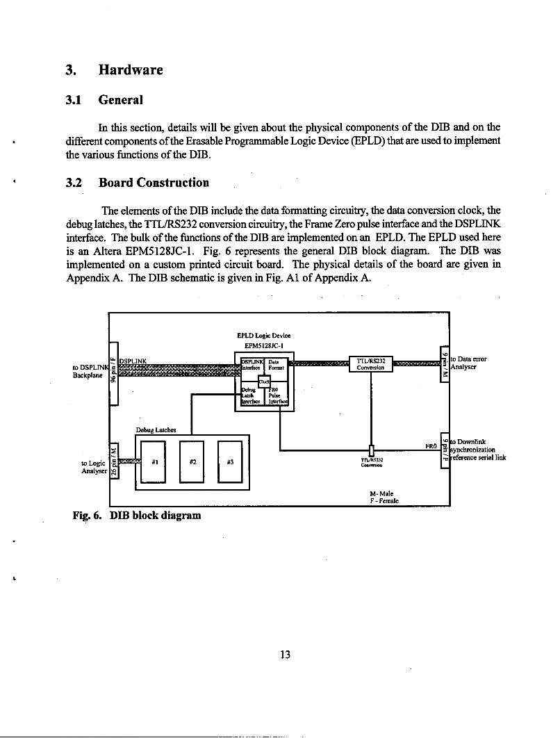
The elements of the DIB include the data formatting circuitry, the data conversion clock, thedebug latches, the TTL/RS232 conversion circuitry, the Frame Zero pulse interface and the DSPLINKinterface. The bulk of the functions of the DIB are implemented on an EPLD. The EPLD used hereis an Altera EPM5128JC-1. Fig. 6 represents the general DIB block diagram. The DIB wasimplemented on a custom printed circuit board. The physical details of the board are given inAppendix A. The DIB schematic is given in Fig. Al of Appendix A.
EPLD Logic Device1 EPM5128JC-1
"DS/at-.RS232 to Data errorto DSPLIN n ~rt222oCovinAaycBackplane
Ss ynchronization
to Logic "-E #1, .rrJR23 eference serial link
M- MaleF - Female
Fig. 6. DIR block diagram
13
3.3 Erasable Programmable Logic Device
The EPLD is an integrated circuit that consists of many macrocells. The collection ofelements or macrocells which are used to implement a particular function in the EPLD produce amacro. A macro can be made of other macros. The EPLD is flexible as it can be erased andreprogrammed to implement modifications for the DIB. The EPLD was found to be very useful inreplacing the numerous small integrated circuits thus reducing the physical space occupied on theboard. The design and programming of the EPLD was done on a personal computer. Substituting oneEPLD for all of the usual integrated circuits meant rapid development of the hardware as well as easycustomization of the hardware interface. The internal chip configuration and the pin usage (input,output or both) are programmed into the EPLD. Modifications can be made on the EPLD by erasingit using ultraviolet light and then reprogramming the EPLD.
The functions implemented in the EPLD include the clock generator, the address decoder asthe logic interface between the DSP and the DIB, the command register, the transmit shift, the receiveshift and status bit generation. These functions are described in greater detail in the followingparagraphs and in Appendix A. The EPLD used in this design is the Altera EPM5128JC-1 whichconsists of 128 macrocells in a 68 pin PLCC package. A schematic of the represented EPLD circuitis given in Fig. A8 of Appendix A.
3.3.1 Clock Generator
The clock generator function of the EPLD provides and distributes the appropriate clock tothe other EPLD functions. This function transforms an external clock signal to the frequency neededby the board to support its operation. The DIB provides two external clock options. The user canprovide the actual 2.4 kHz clock needed for the uplink synchronization experiments, or can providea 432 kHz clock from which the clock generator divides it down to a 2.4 kHz clock. The 432 kHzclock option was initially used in the downlink synchronization experiments [1]. The selection of theexternal clock is made by the DIP switch on the DIB (this is further described in Section 3 ofAppendix B). For the uplink synchronization experiments, the 2.4 kHz external clock is selected.
In the clock generator circuit, the 2.4 kHz clock is called the 'Shift Clock' and is used totransfer data to and from the data sink and source, respectively to satisfy the 2.4 kb/s data rate usedin the uplink synchronization experiments [2]. Another clock is created for internal use, called the'Latch Clock'. The DIB generates the 'Latch Clock' by dividing the 2.4 kHz clock by a factor of 12,thus giving a 200 Hz signal . This is used to signal the DSP when 12 bits of data have beenassembled or disassembled. A schematic of the represented circuit for the clock generator is givenin Fig. A9 of Appendix A.
14

3.3.2 Address Decoder
This EPLD function covers the decoding of the various addresses and sets the base addressof the DIB. The base address is specified by address lines A1,A2, and A3 of the DSPLINK interfaceas described in Section 2.4.1. The selection of the base address is made by the user and is applied bycorrectly setting the DIP switches on the DIB (this is further described in Section 3 of Appendix B).The DIP switch settings are then compared with the corresponding address lines to enable the 3-to-8decoder when there is a match. The 3-to-8 decoder uses address line 0 (AO) and the NWR line togenerate the various I/O port signals required for the DIB (described in Table 2 of Section 2.4.2). Inaddition to the enable signal produced by comparing AO-A3 to the DIP switch settings, the NIOEsignal is also used to enable the 3-to-8 decoder. A schematic of the represented circuit for the addressdecoder is given in Fig. A10 of Appendix A.
3.3.3 Command Register
This EPLD function provides three different operations on the DIB. The command registerenables the user to select whether data is transferred to either the data latch or to one of three debuglatches on the DIB. The command register also allows the user to access the downlinksynchronization reference serial link in order to transmit the FRO pulse. Finally the command registerallows a software reset of the DIB. The operations are identified by specific data bits of the commandregister as described in Section 2.4.2 and are actioned when the Write Command port is accessed.The reset and FRO pulse generation are straightforward in that these operations are carried out bywriting a "0" or a "1" to the appropriate bit. However, as discussed in Section 2, when the userwishes to transfer data to either one of the debug latches or to the data latch for format conversion,the Write Command operation must be followed by a Write Data operation where the actual data istransferred. In this implementation, the Command register bits DO-Dl are used to select thedestination for the data transfer. DO-Di are further decoded to enable the appropriate destinationdevice (data latch or debug latch). A schematic of the represented circuit for the command registeris given in Fig. All of Appendix A.
3.3.4 Transmit Shift
This EPLD function covers the conversion of 12-bit data word stored in a latch into a serialbit stream for the data sink. After being latched, all the data lines are directed into shift registers thatwill convert the data coming from 12 parallel data lines to 12 consecutive bits on a single data line.The Shift Clock (2.4 kHz) described in Section 3.3.1 controls the conversion process. Data from theDSP is transferred in the lower 12 bits of the 16 data lines on DSPLINK. On the DIB, the twelve bitsare shifted out sequentially such that the first bit out of the shift register corresponds to the leastsignificant bit (LSB) of the data word, (i.e. DO). The transmit shift logic interface also provides twostatus bits for the user to monitor data flow through the DIB (TXMT, TXUND). Further details onthe status bit can be found in Section 2.4.2. A schematic of the represented circuit for the transmitshift is given in Fig. A12 of Appendix A.
15

3.3.5 Receive Shift
This EPLD function covers the conversion of a serial bit stream from the data source into a12-bit data word stored in a latch. A data stream is directed into a shift register which, with the helpof the Shift Clock, will transform 12 bits from the data stream to a 12-bit word and store it in a 16-bitdata latch. The data latch consists of the upper 4 bits being zeroed and the lower 12 bits holding the12-bit word assembled by the shift register. The result of the shifting process is that the first bit ofthe data stream is stored in the LSB of the data latch (i.e. DO). The receive shift logic interface alsoprovides two status bits for the user to monitor data flow through the DIB ( RXRDY, RXOVR).
This macro also contains the circuitry for assembling the DIB status bits that form the statusregister. The description of the status bits was given in Section 2.4.2. A schematic of the representedcircuit for the receive shift is given in Fig. A13 of Appendix A.
3.3.6 Status Bit Generation
In both the "Transmit Shift" and "Receive Shift" macros, there are two macros which areidentified in the schematics as "RiseDet" and "DFFPlus". They are used to generate the 4 statusbits that are related to the data transfer and format conversion (TXMT, TXUND, RXRDY, RXOVR).In the "RiseDet" macro, a D-type flip flop is connected so that on the rising edge of the 200Hz"Latch Clk", a "high" signal is generated at the output. This signal is used to signal when data isready to be read by the GT (i.e. RXRDY) or when the DIB is ready for the next data to be sent bythe PL (i.e. TXMT). The "high" signal is cleared when the GT or PL subsequently reads or transfers,as appropriate, the next data word. The "DFFPlus" macro follows the "RiseDet" and consists ofanother D-type flip flop used to latch the output of the "RiseDet" macro. The same 200Hz "LatchClk" is used as the clock signal. If the output of the "RiseDet" macro has not been cleared beforethe rising edge of the clock signal, then the output of the "DFFPlus" macro will latch a "high" signalto its output. The output of the "DFFPlus" is used to signal when data has been overwritten becauseof an overflow at the GT simulator subsystem (i.e. RXOVR) or when data has not been madeavailable by the PL simulator subsystem thereby causing an underftow condition (i.e. TXUND).Schematics of the represented circuit for the "RiseDet" and "DFFPlus" are given in Fig. A14 andA15 of Appendix A.
3.4 Debug Latches
There are three 16-bit debug latches on the DIB which can be used as a debugging tool. Each16-bit latch is composed of two octal D-flip-flops. The configuration of the latches is such that thereis a one-to-one correspondence of the DSPLINK data lines to the debug latch data lines. All threedebug latches can be accessed at any time by the user. The debug latches can be read by probing the
16

integrated circuit. In addition, debug latch #1 can also be read directly from a 26-pin connectormounted at one end of the DIB. Details of the 26-pin connector are included in Section 2.2 ofAppendix A.
3.5 External Interfaces
There are four external interfaces on the DIB. The first is a 96-pin connector which isconnected to the DSP backplane developed for the uplink synchronization experiments and providesthe interface between the DSP and the DIB. The DSP backplane includes the DSPLINK expansioninterface of Spectrum Signal Processing Inc. DSP boards. The DSPLINK interface [4] is a high-speed, bidirectional bus that allows data transfer with the DSP, thereby avoiding the PC busbottleneck. The DSPLINK supports 16-bit data transfers. The signals which make up the DSPLINKinterface and are used for the DIB are described in Section 2.4. The DIB can be driven by any of theSpectrum Signal Processing Inc. DSP boards which support the DSPLINK interface. Two 9-pinRS232 connectors are also present on the DIB. One RS232 connector is used for the downlinksynchronization reference serial link which carries the FRO pulse. The other RS232 connector is forthe data source or sink connection. A 26-pin connector is also available and provides off-boardaccess to debug latch #1. The four external interfaces are described in Appendix A.
17

4. Testing
A description of the testing done on the DIB is given in the following section. The purposeof testing is to verify the three functions of the board: data conversion/transfer; transmission anddetection of the Frame Zero pulse; and use of debug latches. The setup used for testing is illustratedin Fig. 7. For testing purposes only, the clock required for the operation of the DIB is provided bya function generator.
4.1 Test Setup
Upon initial completion of the DIB, all the functions of the DIB were verified for properoperation. Fig. 7 illustrates the test setup for the DIB. As the DIB implements both the functions forthe GT and the PL simulator subsystems, a single DIB is set up in a loop back configuration so thatdata flowing in both directions can be tested.
The external clock was generated by the function generator shown in Fig. 7. The Xantraxpower supply was used for DC power necessary for the board to operate. The power supply is usedonly for the test setup as the DIB is installed in a DSPLINK backplane which provides power for theDIB during the uplink synchronization experiments. The data error analyser was used as both thedata source and sink to verify the data flow from the source to the destination. The FROout andFROin lines are connected together so that when a FRO pulse is transmitted, it is immediatelyreflected on the status register of the DIB. The test program used can be found in Appendix C. Adescription of the tests carried out for each of the functions is included in the following paragraphs.
Wire HP 1645
HP3314A LXQ203 Data error
Function Power strobe path analyser
Generator Source I - + RS232 I(Source /sink)
I IData/C~
432 kHz wire I ICIk (coax) 5V,
±15'V
DIB
PC
50 to 96 pin
adaptor board
Fig. 7. Test setup diagram19

4.1.1 Data Conversion/transfer test
The purpose of the test is to verify that the onboard (DIB) data conversion and transfer arebeing performed successfully.
The raw data came from the data error analyser (HP 1645) and is sent through the DIB whereit was transformed from a single bit stream into consecutive 12-bit words and sent to the DSP boardinstalled inside a PC (simulated subsystem). Once on the DSP board, the data was written back tothe DIB and reformatted from 12-bit words to a single bit stream. The data was then forwarded tothe data error analyser. More information on data operation can be found in section 2.3.1.
To verify that the data has successfully been received, transmitted and transformed, the dataerror analyser was monitored during the testing. The testing process was repeated several times toensure reliability. The indicator on the data error analyser read "0" meaning that the conversion andtransfer portion of the DIB was working properly. Therefore, the testing of this portion wassuccessful.
The listing of the test program for the DIB data conversion and transfer can be found in
Appendix C of this document.
4.1.2 Tx/Rx Frame Zero test
The purpose of this test was to verify that the transmission and reception of the Frame Zeropulse were being performed successfully.
The Frame Zero pulse was generated by the TMS DSP board using the DIB command registercausing a pulse on the J5 connector. For testing purpose, a cable was connected between the outputof the Frame Zero port and its input, creating a loop back of the Frame Zero pulse. Once the pulse islooped back on the DIB, it can be read by the DSP from the DIB status register. Therefore, both thereception and the transmission of the Frame Zero pulse are tested simultaneously. To verify that theFrame Zero pulse was successfully transmitted and received, a logic analyser was also used tomonitor the Frame Zero pulse port. The reader is referred to Section 2.3.2 for more information onthe timing of the Frame Zero pulse.
The listing of the test program for the DIB Frame Zero pulse can be found in Appendix C ofthis document.
20

4.1.3 Debug latch test
The purpose of the test is to verify that the onboard 16-bit latches work properly.
The testing of the debug latches consists of simply writing a user-defined 16-bit word ontodebug latch #1 and monitoring the data lines of the latch via the external connector. In addition, thedebug latch operation was tested to ensure it did not affect the other functions of the DIB. This wasverified to be true. The test was performed and was successful for all three debug latches. The readeris referred to section 2.3.3 for more information on the debug latches.
The listing of the test program for the DIB data conversion and transfer can be found inAppendix C of this document.
21

5. Conclusion
A multipurpose DIB was designed and implemented for upcoming uplink synchronizationtrials at DREO. The DIB can be used in both the GT and PL simulator subsystems. The DIB formatsa serial bit stream of data from an HP 1645 data error analyser into consecutive 12-bit words to betransferred to the GT processor for data transmission. Prior to formatting the bit stream, the DIBconverts the original RS232 level signal to TTL levels required for the DIB circuitry. The reverseoperation is also performed by the DIB for the PL processor side. The DIB also provides the interfacebetween the GT and PL simulator subsystems and the downlink synchronization reference serial link.The link is used to carry a reference of the PL system clock, called the FRO pulse, that is generatedby the PL. The FRO pulse is used by the GT as a starting point for uplink synchronization. Again,this interface includes the TTL/RS232 conversion of the reference signal. The DIB also providesthree 16-bit debug latches for the user to use as a debug tool. Data lines from one of the three latcheshave been brought out to a connector for easier access.
The DIB was implemented and fabricated on a custom PCB. Flexibility was a key aspect ofthe DIB design. In addition to designing both the GT and PL requirements for data formatting andconversion on the same board, an EPLD was used to minimize the number of ICs on the board.Substituting the various circuits by an EPLD meant rapid development of the hardware as well aseasy customization of the hardware interface. The EPLD is currently programmed to 80% of itscapacity. The circuits incorporated into the EPLD include the interface between the DSP and theDIB, the data formatting operation, clock signal generation, and command and status registeroperations.
The DIB is driven by either a GT or PL processor. The processors for the uplinksynchronization trials are implemented on Spectrum DSP boards and have a DSPLINK interface. TheDSPLINK interface was implemented on a backplane which contains the DIB as well as other custominterface boards used in the experiments. The DIB is also connected to a data device (HP1645) aswell as a downlink synchronization reference serial link.
A user's guide is provided in an Appendix B which describes the proper configuration andoperation of the DIB. The DIB was tested and all the functions were verified to work properly.Appendix C includes the program written for the Spectrum TMS320C25 DSP board to independentlytest the DIB.
23

References
1. Addison, R., Seed, W., "Implementation of an EHF Frequency-Hopping Simulator", DREOReport 1279, December 1995.
2. Lambert, J.D., "DREO/CRC Joint Data Link Standard for Low Data Rate Service to EHFGround Terminal Payload Simulators", DREO Report 1069, February 1991.
3. Addison, R., "Modified Hopping Synthesizer Controller", DREO Report 1304, December
1996.
4. TMS320C25 Processor Board User's Manual, Spectrum Signal Processing, Inc. Version 2,September 1988.
5. The TTL Data Book, Texas Instruments, Volume 2, 1985.
6. MAX+PLUS, Programmable Logic Development System, ALTERA Corporation, 1995.
25
Appendix A: Hardware & Firmware Details
1. General
This appendix contains the schematics, component list and layout of the DIB. The custommacros of the EPLD for the DIB functions can also be found in this appendix. The external interfaceconnectors of the DIB are also described.
2. DIB
In this section of Appendix A, a graphic description of the circuitry of the DIB, its hardwarecomponents and its layout description can be found.
2.1 Schematic
The schematic for the multipurpose DIB is given in Fig. Al
Al

B~ I'
c~~l v Izi r~a
"a
1A2Ra~9 1 BgBB

2.2 Layout Description
The printed circuit board layout of the DIB is shown in Fig. A2. All parts are standard off-the-shelf. The EPLD is the only component that will need to be modified (programmed). ThisEPLD contains most of the interface logic for the address decoder, data formatting, the clock signalgeneration, command and status register operations. Fig. A2 reveals the position of the six 8-bitlatches used to form the three 16-bit debug latches which are used for debugging purposes. Linedrivers used to convert TTL signal to RS232 signal and vice versa are also shown. The buffers areused to isolate the signal for DSPLINK lines coming from DSPLINK backplane. There is an unusedIC socket on the board (Spare) to allow an TTL IC to be implemented for debugging purposes or forfuture expansion.
RS232 ',9-pin/ I
Front Pane S232 9-Ain/F J4 (26-pin/M)
Lin D i e s ..... ar.e...... .• .. • . ••••°• °-.......................,
• 1 .....•;...........U7 I ' ' II
I #1 LSB
US U10
#2 LSB.°.....................
U12
EPLD #3 LSB
EPM512SJC-1 27, 7
#1 MSB
Swi 1)W on
#2 MSB
LSB: Least Significant Bi : #3M5(DO - D7) #3 MSB
M SB: Most Significant B 43tife ...............
I Capacitor 0.01 tF 03 02 01
* Capacitor 1 pFC9-C13
M - male + arpt 0r"2 *Fps O*"d
FM fmaleF - female --• Backplane Conneto J)(6pnM
Fig. A2. Multipurpose DIB printed circuit board layout
A3
2.3 External Interface Connectors
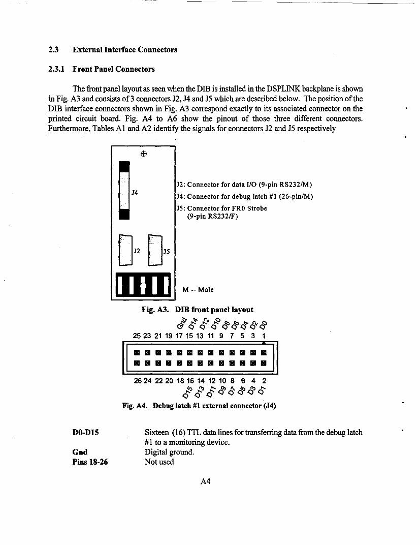
2.3.1 Front Panel Connectors
The front panel layout as seen when the DIB is installed in the DSPLINK backplane is shownin Fig. A3 and consists of 3 connectors J2, J4 and J5 which are described below. The position of theDIB interface connectors shown in Fig. A3 correspond exactly to its associated connector on theprinted circuit board. Fig. A4 to A6 show the pinout of those three different connectors.Furthermore, Tables Al and A2 identify the signals for connectors J2 and J5 respectively
+
J2: Connector for data I/O (9-pin RS232/M)J4: Connector for debug latch #1 (26-pin/M)
J5: Connector for FRO Strobe(9-pin RS232/F)
[]2 J5
[ l M -- Male
Fig. A3. DIB front panel layout
25 23 21 19 17 15 13 11 9 7 5 3 1
26 24 22 20 18 16 14 12 10 8 6 4 2
Fig. A4. Debug latch #1 external connector (J4)
DO-D15 Sixteen (16) TTL data lines for transferring data from the debug latch#1 to a monitoring device.
Gnd Digital ground.Pins 18-26 Not used
A4
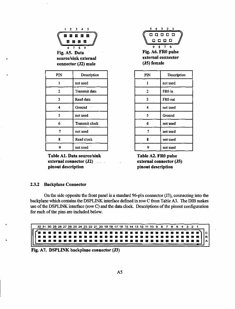
1 2 3 4 5 5 4 3 2 1
6 7 8 9 9 8 7 6
Fig. A5. Data Fig. A6. FRO pulsesource/sink external external connectorconnector (J2) male (JB) female
PIN Description PIN Description
I not used 1 not used
2 Transmit data 2 FRO in
3 Read data 3 FRO out
4 Ground 4 not used
5 not used 5 Ground
6 Transmit clock 6 not used
7 not used 7 not used
8 Read clock 8 not used
9 not used 9 not used
Table Al. Data source/sink Table A2. FRO pulseexternal connector (J2) external connector (J5)pinout description pinout description
2.3.2 Backplane Connector
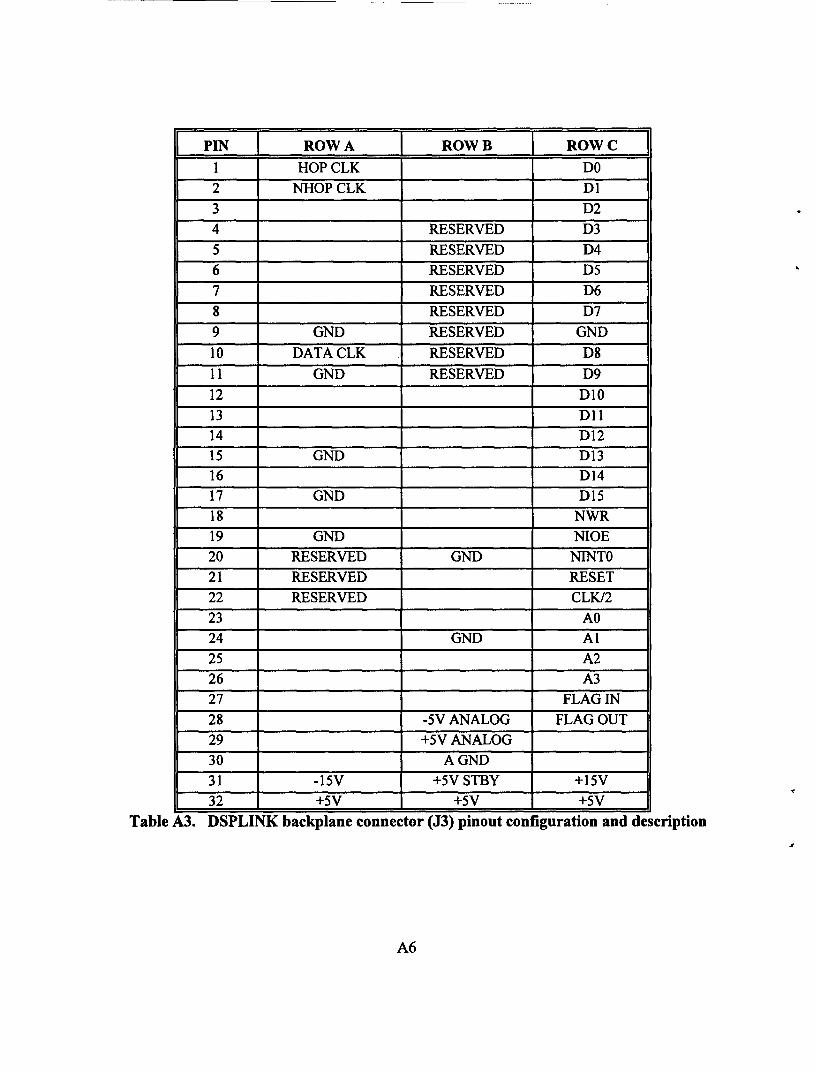
On the side opposite the front panel is a standard 96-pin connector (J3), connecting into thebackplane which contains the DSPLINK interface defined in row C from Table A3. The DIB makesuse of the DSPLINK interface (row C) and the data clock. Descriptions of the pinout configurationfor each of the pins are included below.
32 31 30 29 28 27 26 25 24 23 22 21 20 19 18 17 16 15 14 13 12 11 10 9 8 7 6 5 4 3 2 1
Fig. A7. DSPLINK backplane connector (J3)
A5
"PIN ROW A ROW B ROW C
1 HOP CLK DO2 NHOPCLK DI3 D2
4 RESERVED D35 RESERVED D46 RESERVED D5
7 RESERVED D68 RESERVED D7
9 GND RESERVED GND
10 DATA CLK RESERVED D8
11 GND RESERVED D9
12 D10
13 DlI14 D1215 GND D1316 D1417 GND D1518 NWR19 GND NIOE20 RESERVED GND NINTO
21 RESERVED RESET22 RESERVED CLK/2
23 AO24 GND Al25 A226 A327 FLAG IN28 -5V ANALOG FLAG OUT
29 +5V ANALOG30 AGND
31 -15V +5V STBY +15V32 +5V +5V +5V
Table A3. DSPLINK backplane connector (J3) pinout configuration and description
A6

DO-D15 Sixteen bi-directional TTL data lines of DSPLINK
GND Digital groundNWR DSPLINK read/not write line originating from the
DSP to signal the direction of data transfer. The "notwrite" nomenclature denotes an active-low signal forthe WRITE signal. The direction is determined fromthe point of view of the DSP (i.e. a WRITE refers todata being transferred from the DSP to the DIB.
NIOE An active-low, input/output enable signal indicatingan access on the DSPLINK originating from the DSP.
NINTO A negative-edge triggered, or active-low interruptsignal on DSPLINK. This signal is not used by theDIB.
RESET DSPLINK reset line. This signal is active-low.
CLK/2 General purpose clock signal on DSPLINK originatingfrom the DSP. This signal is not used by the DIB.
AO-A3 Four buffered TTL address lines of DSPLINK.FLAGIN General purpose input line on DSPLINK readable by
the DSP. This signal is not used by the DIB.FLAGOUT General purpose output line on DSPLINK writeable by
the DSP.15V 15 volts power supply.-15V -15 volts power supply5V 5 volts power supply
-5V ANALOG -5 volts analog power supply5V ANALOG 5 volts analog power supply
AGND Analog ground5V STDBY 5 volts standby power supply. This signal is not used
by the DIB.HOP CLK Hop clock signal provided by another source. This pin
is not used by the DIB.
NHOP CLK Inverse hop clock signal. This pin is not used by theDIB.
DATA CLK Data clock signal provided by another source to theDSPLINK backplane.
RESERVED Reserved lines for the DSPLINK backplane.
A7

2.4 Key Component List
A list of the components which were used for the DIB are provided in Tables A4, A5, andA6. The component labels listed in each of the tables correspond to the labels used on the printedcircuit schematic in Fig.A1.
2.4.1 Integrated Circuits
Board Component Type JName
U1, U2 74LS245 Octal bus transceiver
U3 74LS244 Octal line driver
U4 EPM5128JC-1 Altera 128 macro-EPLD, 30 ns
U5 74ALS240 Octal inverting line driver
U6 MC1488 Quad line driver
U7 MC1489 Quad line receiver
U8,U9,U10,U1 1,U12,U13 74LS273 Octal D flip-flop with clear
Table A4. Integrated circuits
2.4.2 Discrete Components
Component [Type
DC1 - DC13 0.01 gF
RESDIP Resistor DIP, 7 wide, 20 kQ
C9 - C13 10 gF Tantalum
TP1 - TP4 Test point postTP 1: monitors line B31 on J3 (+5V STBY)TP2: monitors line A22 on J3 (free)TP3: monitors line A27 on J3 (free)TP4: monitors line A29 on J3 (free)
Switch (SW1) DIP switch, single throw, 7 wide
Spare Unused socket position available for expansion
Table A5. Discrete components
A8
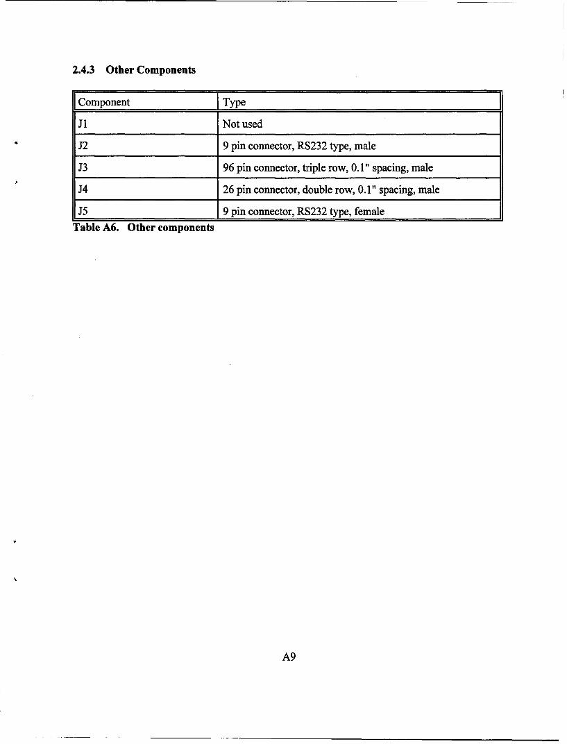
2.4.3 Other Components
Component Type
Ji Not used
J2 9 pin connector, RS232 type, male
J3 96 pin connector, triple row, 0.1" spacing, male
J4 26 pin connector, double row, 0.1" spacing, male
J5 9 pin connector, RS232 type, female
Table A6. Other components
A9

3. EPLD Description
3.1 General
This section graphically describes the firmware used in the EPLD Altera EPM5128JC-1. TheEPLD was configured with the MAX+plusIl compiler installed in a PC and then loaded on the EPLDchip using an interface board and a programming unit.
3.2 EPLD Schematics
The EPLD, Altera 5128, is an erasable programmable logic device that replaces a collectionof TTL logic and reduces significantly the number of ICs. The EPLD is programmed using theMAX II + Plus software from Altera. At present, the macros have used about 80% of the EPLDspace. The EPLD schematic shown in Fig. A8 includes several custom macros in order to simplifythe total logic circuit of the EPLD. Each macro is identified by the box drawn in a dotted line. Thecustom macros are listed in Table A7. Each of the macros are described in the following sections.
Macro Name Description of Macro Reference Fig.
Clocks Clock generation Fig. A9
Address Address decoder Fig. AlO
Comdreg Command register Fig. Al 1
TxShift Transmit Shift - conversion from Fig. A1212-bit word to a 1-bit datastream
RxShift Receive Shift - conversion from Fig. A13a 1-bit data stream to a 12-bitword
RiseDet Rise Detector - status bit Fig. A14generation
DFFPlus D-flip-flop Plus - status bit Fig. A15generation
Table A7. List of EPLD Macros for the DIB Functions
All

- - ----- 171 F - F-7 F -1 Iw I I I mI I WMI I
@ E:$: c! l* i I cu M 0 :
0' (3: (J: (3 W.
00000000000a 00a 0:; la 0 IL
; f.,-. fr- 0 if- frf- f
16Ic
c zLic it3
... .. .. .. . .. . A .l . .. . .. . . . . . . . .
00u L
x 0L 1 L. x m 1
Ii c 0 at. .PJ I. -. hi hi a a I
a C wi I--o -iJ ICI I9 IC 9 2CI
a- z z z 2 x t.. .....
....I. L I ......... ......vA12

3.2.1 Clock Generator Macro
The clock generation macro shown in Fig. A9 produces two clock signals which are requiredfor the data transformation process. The two clock signals required are a 2.4 kHz data clock signaland a 200 Hz clock signal. The 2.4 kHz signal is used to shift the bit stream to and from the datadevice. The 200 Hz signal, derived from the 2.4 kHz data clock signal is used for moving 12 bitsof data.
There are two ways in which the two clock signals may be generated. The first method isa straightforward one where the 2.4 kHz data clock signal is directly provided by the user via theexternal clock input on the DIB. This is represented by the XClk_2400 signal from Fig. A9. The200 Hz signal is subsequently produced by dividing the 2.4 kHz signal using a divide-by-12 circuit(7492). The divide-by-12 process actually occurs in two stages: a divide-by-2, followed by a divide-by-6 stage as indicated by the feedback from the QA output to the CLKB input of the 7492 device.The resulting 200 Hz signal, labelled Clk_200, is produced at the QD output of the divide-by-12circuit.
The second method for producing the required clock signals consists of the user providinga 432 kHz clock signal via the external clock input on the DIB. The 432 kHz input signal optionoriginated from requirements for the DIB used in the downlink synchronization experiments. Thisoption was retained to allow flexibility in expanding the number of clock signals that could begenerated. The clock generation macro again divides the 432 kHz input clock signal to produce therequired signals. The generation of the 2.4 kHz signal is achieved by dividing the input clock signalby 180. This is implemented in two stages: a divide-by-90 and a divide-by-2 stage. The divide-by-90 function is effected by an 8-bit up/down counter which is loaded with an initial value of 90. Inthis implementation, the counter is configured to count down. When the counter reaches "0", it isreset and reloaded with a value of 90 and the process is repeated. The output of the down counteris a 4.8 kHz (432 kHz/90) signal which is then divided by two via a toggle flip-flop (TFF in Fig. A9)to produce the needed 2.4 kHz. As in the first method, the required 200 Hz signal is generated bydividing the 2.4 kHz by 12 as described in the previous paragraph.
A multiplexor is used to allow the user to select which method is used by the EPLD toproduce the required clock signals. The selection is determined by the Sel_2400/N432 line shownin Fig. A9. When the line is "high", the 2400 Hz clock is used. Conversely, when theSel_2400/N432 line is "low", the option to use a 432 kHz signal as the input clock signal is selected.The Sel_2400/N432 line is set by a dip switch on the board which is described in Appendix B.
A13

xw
ww
12:
0~~ LL
a .6*
o r -7zu
1 x 3£ z
10.
A1

3.2.2 Address Decoder Macro
The address decoder macro is illustrated in Fig. A10. The address decoder generates the 1/0port select lines for the EPLD. The I/O port select lines are labelled NWrData, NRdData,NWrComd, and NRdStat. These lines correspond to Write Data, Read Data, Write Command,and Read Status respectively described in Section 2.4.2 in the main document. The four I/O portselect lines are represented by four outputs of a 3-to-8 decoder. The select lines are generated bydecoding the NWR (read/write) line and the AO address line both from the DSPLINK interface. Athird input is tied to ground. A 3-to-8 decoder was used rather than a 2-to-4 decoder to facilitatefuture expansion.
With the 3-to-8 decoder, two enable signals are available for the address decoder macro toensure that a valid I/O access is taking place and that the DIB is being addressed. The first enablesignal is provided by the NIOE signal from the DSPLINK interface. The NIOE is an active-lowsignal which is generated on DSPLINK when the DSP initiates an I/O access to an external board.The other enable signal is provided by the output of a comparator which is included in the addressdecoder macro. The comparator is used to verify the base address of the I/O operation. The baseaddressing scheme ensures that multiple interface boards using the DSPLINK do not use conflictingaddresses and is described in Section 2.4.1 of the main document. The dip switch settings of theDIB for selecting the base address are compared with the Al, A2, and A3 address lines of the I/Ooperation. A "low" signal is produced at the comparator output only if the base address used by theDSP matches the dip switch settings.
In order to isolate the data lines on the DIB from the DSPLINK data lines when the DIB isnot being addressed, two 8-bit buffers, 74LS245, are used on the DIB. The 74LS245 buffers includean enable line which can be used to disable the device, effectively isolating the data lines. Anadditional signal, NBufEn, is generated in the address decoder macro to perform this function. TheNBuf En signal is an active-low signal which is generated by a logic OR of the NIOE signal and theoutput of the comparator. In other words, a "low," signal is produced to enable the buffers when botha valid I/O operation is occurring (NIOE is "low") and the board is selected (output of thecomparator is "low").
A15

:Z:Z: Z: Z:
z z z i z z z
C', Z
00
0 cc ri) L 0IL 0 IL 0JL IL JL jLa tojh1* zz *
~UNas
.4 Z
0 w0
... 4:
~]LiLL iiUA1

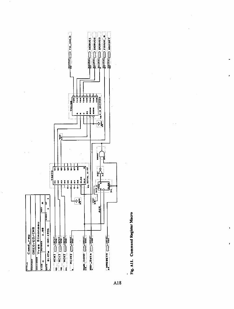
3.2.3 Command Register Macro
The ComdReg macro is illustrated in Fig. Al1. The ComdReg macro provides thenecessary logic to allow the user to select whether data is to be transferred to the data buffer or toone of three debug latches on the DIB. It also allows the user to issue a software reset of the DIBor to send a FRO pulse. These operations are described in Section 2.4.2 of the main document.When a Write Command operation is performed by the DSP, the NWR COMD select line generatedby address decoder macro causes data lines A[O], A[l], and A[2] to be stored in a latch and A[15]to be stored on a flip flop. A[O], A[1], A[2], and A[15] correspond to the data bits (DO, DI, D2, andD15 respectively) on the command register described in Section 2.4.2. Hence, A[O] and A[l] arethe data destination selection lines, A[2] is the FROout line, and A[15] is the software reset line.When the FRO-out line is latched, the output of the latch, labelled FRAME 0 in Fig. A.11, istransferred directly to the TTL/RS232 conversion circuitry. The software reset line is combined withthe DSPLINK reset line, NRESETH, to generate the board reset line, NRESET. The inclusion ofthe DSPLINK reset line allows the DIB to be reset using either a hardware or software reset.
As the DIB allows the user to transfer data to multiple locations on the DIB, a second levelof decoding is required to produce the appropriate select line for transferring data to the DIB. Theselect lines, TxHold, DEBUG_1, DEBUG_2, and DEBUG_3 are generated by decoding the latchedA[O] and A[l] lines, labelled Q1 and Q2 in Fig. A9, using a 3-to-8 decoder. Again, a 3-to-8 decoderis used in lieu of a 2-to-4 decoder to allow additional select lines to be generated in the future ifrequired. The generation of the appropriate select line takes place upon a Write Data operationwhereby a "low" NWrData signal is produced from the address decoder macro to enable the 3-to-8decoder. The actual data transfer occurs during the Write Data operation.
A17
0 .5: M: C: W,
:W: w. :w. :Q: 2M
3- 2. 2 1.- 2
I XI
c a1 0
.. ... ...
14 q v 1 Z1 .
w a & a a L

3.2.4 Transmit Shift Macro
The purpose of the TXShift macro is to take a 12-bit word, transferred from the DSP, andconvert it to a single bit stream that is to be forwarded to the data sink. The 12-bit word is locatedin the lower 12 bits of the 16-bit DSPLINK data interface. From Fig. A12, the 16 data lines fromthe DSPLINK interface, labelled A[15..0], lead to two 8-bit latches. Data on the lines are stored onthe latches upon the rising edge of the TxHold signal. The TxHold signal is the I/O port selectline generated by the secondary level of decoding of the command register bits DO and D1 whichis described in Section 4.2.3 of this appendix. The TxHold signal is selected or active during aWrite Data operation where the data buffer is selected as the destination of the data transfer (i.e. DOand D1 of the command register are both zero). The latched data is transferred to two 8-bit shiftregisters which are connected in series. The data is "shifted" out one bit at a time on the DataOutline using the ShiftClk signal. For the uplink synchronization experiments, the ShiftClk is the 2.4kHz clock provided by the user. It is noted that the data lines are bit reversed between the datalatches and the shift registers so that the least significant bit (LSB) is shifted out first. The shiftprocess is controlled by the LatchClk signal which is generated by dividing the 2.4 kHz data clockby 12 yielding a 200 Hz signal (See Section 4.2.1 of this appendix). The LatchClk signal is usedto generate a low signal to load the next 16-bit word from the data latches to the shift registers. Bygenerating the load signal using the LatchClk, the shift process is effectively limited to 12 bits afterwhich the next data is transferred to the shift registers.
There are also two status lines which are generated by the TXShift macro. They are theHid-Empty and Hld_Under lines, which allow the user to monitor the data flow process of thismacro. The two lines correspond to the TXMT and TXUNND bits of the status register as describedin Section 2.4.2 of the main document. The Hld_Empty signal is generated by a flip flop circuitdefined under the RiseDet macro which is described in Section 4.2.6 of this appendix. A "high"signal is produced on the Hid_Empty line on every rising edge of the LatchClk to signal that the16-bits from the data latch have been transferred to the shift registers and that the data latches areready to store the next 16 bits. The Hld_Empty signal is cleared only when the next 16-bits aretransferred from the DSP, i.e. when a TxHold signal is generated. If no data is transferred to thedata latches by the next rising edge of the LatchClk, the "high" level HldEmpty signal is latchedonto the HId_Under line indicating that an underflow condition has occurred.
A19

.48
L 0.)I1 J
:1 L '
I.8. a. tm
.0 a al
L16
CODo c a. . : . 0
ai LL . Jo "03 0 03
4 J- 4E~ goI.-
. W 1* 0 ..*J 'a
I d oi:a
..x m >-L >z
ILA20

3.2.5 Receive Shift Macro
In the RXShift macro, there are two separate circuits which are implemented. The first isthe transformation of a bit stream of data coming from a data source, the DataIn line in Fig. A13to a 12-bit word. This process is basically the reverse of that described for the TXShift macro. Thesecond circuit contains the logic required to form the status register which is read by the DSP.
For the data transformation, two 8-bit shift registers are connected in series as for theTXShift macro. A single bit stream of data (DataIn) is shifted into the shift registers using the 2.4kHz ShiftClk signal. When 12 bits have been shifted in, the Latch_Clk signal will trigger the 12bits to be transferred in parallel to the internal latch with the 4 upper bits tied to ground. When aRead Data operation occurs, the multiplexor transfers the data lines from the internal latch to a 16-bitbuffer where it can be read by the DSP.
The status register is defined by 5 bits as described in Section 2.4.2 in the main document.The lines labelled "S 15" and "S 14" are related to the data transformation process described in theparagraph above and correspond to status bits RXRDY and RXOVR. The two lines are generatedin the same manner as the Hid_Empty and Hld_Under lines in the TXShift macro described earlier.For the RXShift macro, a "high" signal is generated at the output of the RiseDet macro on everyrising edge of the Latch_Clk. This "high" signal is the RXRDY signal on the status register whichinforms the DSP (user) that 12 bits are available to be read. The RXRDY signal is cleared when thedata is read from the buffer. If the data is not read by the time the next 12 bits are available, a secondflip flop (labelled DFFPlus) produces a "high" RxDataOverflow ( or RXOVR on the statusregister) signal indicating an overflow condition has occurred. The third and fourth bits of the statusregister are the Hid_Empty and Hid_Under lines which are produced by the TXShift macro. Thefifth status bit is the FRO line from the separate serial link connecting the PL and the GT. The fivestatus bits are presented to the other port of the multiplexor with the lower 10 bits set to "0". Duringa read status operation, where the NRdStat line becomes active ("low"), the status register bits aretransferred through the multiplexor to the buffer (labelled, TriB) to be read by the DSP.
3.2.6 Rise Detector Macro and D flip-flop Macro
The RiseDet and DFFPlus macros, shown in Fig. A14 and A15 respectively, are used inthe TXShift and RXShift macros to generate the status register bits. They are both based on a D-type flip flop and are cleared by an appropriate NClr or NReset board reset signal. The selection ofthe NClr signal is discussed in the TXShift and RXShift macros. The NReset signal is describedin the ComdReg macro.
In the RiseDet macro, the input of the D flip flop is tied to Vcc. Consequently, on the risingedge of the Clk signal, the RiseDet macro produces a "high" signal at its positive output. Theoutput is cleared (i.e. returned to "0") only when an active-low NCLR or NRESET is received. Thismacro is used to generate the two status bits TXMT and RXRDY as described in Section 4.2.4 and4.2.5 above.
A21
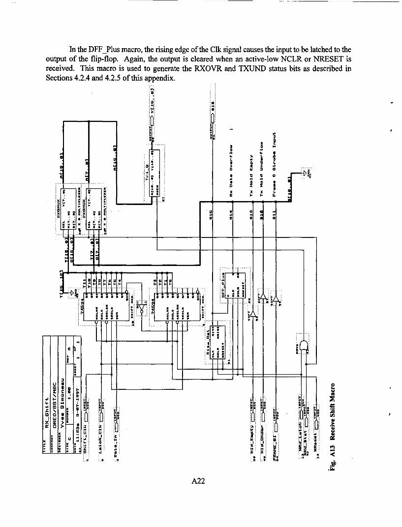
In the DFFPlus macro, the rising edge of the Clk signal causes the input to be latched to theoutput of the flip-flop. Again, the output is cleared when an active-low NCLR or NRESET isreceived. This macro is used to generate the RXOVR and TXUJND status bits as described inSections 4.2.4 and 4.2.5 of this appendix.
w IX
I. I- L
LO q 0*u .4 " 4. U
X~ FA
.... .. ......
:14 0 M~I
j a 6 1o o 09to... 5 .. ... .........
1 0 0.5
03 a 2
*~~~~~I .1...1 -4 I- S(I S .
I A:I
V V04W4.C~P4 Pq4U4
U.iz.,
A22 ~ O
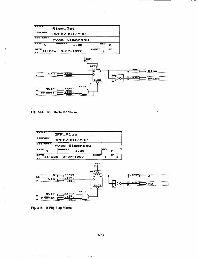
TI TLER i se-Det
coflpnmyDREO/SBT/MSC
DES I SNERYvem Simoneau
SIZE A unBER 1.0REV A
D RTE SHEET OF
f,11:22a 3-87-1997 1 ± J
1P1
D -= Rise
Fig A1m ...- RiseDt
to Ma r
TI TLEDFF-Pl1us
COMPANY
DREO/66T/MSCDES I ONER
Yves SimoneauSIZE A NUMBER 1.00 REV A
DATE SHEET OF11:22a 3-87-199
.. ...... ... .. . . .. ..
Fig..... A15 D-~pFo Acro
A23

Appendix B: DIB User's Guide
1. General
This appendix covers the information required to install, configure and use the DIB. Thelatter consists of a description of the modes of operation and examples of working with the DIB.The examples given are: reading the status; giving a command; reading the data from a data source;sending the data to a data sink; resetting the DIB; writing to the debug latches; andtransmitting/receiving the FRO pulse. Sample code for each of these operations is included.
2. Installation
In order to facilitate the implementation of all the interface boards for the uplinksynchronization experiments, a chassis which provides a DSPLINK interface and additional clocksignals on a single backplane is used. The DIB is installed by sliding it onto the backplane,connecting its 96-pin connector to the rear of the backplane itself. The backplane is connected tothe DSP by an extension card and a 50-pin ribbon cable. The extension card was fabricated to mapthe 96-pin backplane to the 50-pin DSPLINK interface on the DSP board. It is recommended thatthe cable from the backplane to the computer be no longer than 3 feet to minimize losses whichwould corrupt the signal.
Once the board is correctly installed onto the backplane, the connections to the front panelcan take place. The data port, labelled as J2 in Fig.A3, should be connected by an RS232 cable toa designated data device. For the uplink synchronization experiments, the data device used is theHewlett Packard 1645 data error analyser. The DIB will either send serial data through that port orreceive it.
The FRO port, labelled as J5 in Fig.A3, is connected to the FRO port of another DIB via aseparate RS232 cable to realize the downlink synchronization reference link. In the uplinksynchronization experiments, the RS232 cable from the DIB located at the PL simulator subsystemis connected to one of the ports of a statistical multiplexer (stat mux). The stat mux is connected toa serial communication link setup between the transmit and receive locations at DREO/CRC. At theother end of the serial link, the connection is passed through another stat mux to the port connectedto the FRO port of the GT DIB.
A 26-pin connector is also provided to the user to access the data lines for debug latch #1.This facilitates the use of a logic analyser to observe the data stored on the debug latch. The datalines for debug latches #2 and #3 may be accessed by probing the chip.
BI

3. Configuration
In the middle of the DIB, a 7-pin wide DIP switch is accessible (see Fig. Al of Appendix A).The switch is used to configure the board and includes the selection of the base address of the DIB.The details of the DIP switch settings are given in Table B 1.
Switch Selects I Position TTL Value Value
SWI Not Used X X X
SW2 External Clock Closed/On 0 432 kHzSelection Open/Off 1 2.4 kHz
SW3 I/O Format Closed/On 0 RS232Open/Off 1 TTL (not used)
SW4 Not Used X X X
SW5 Base Address Closed/On 0 Disabledselection/ Open/Off 1 EnabledAddress Line #3(MSB)
SW6 Base Address Closed/On 0 Disabledselection/ Open/Off 1 EnabledAddress Line #2
SW7 Base Address Closed/On 0 Disabledselection/ Open/Off 1 EnabledAddress Line #1 (LSB) I I
(X - don't care)Table B1. Configuration DIP switch settings.
The switches, that are being used, are described in the following paragraphs.
External Clock Selection (SW2): The DIB can work with two different input external clockspeeds. One being at 2.4 kHz and the other at 432 kHz. The default setting is at 2.4 kHzwhich is the rate required for the uplink synchronization trials.
I/0 Format (SW3): The DIB is designed to be able to transmit and receive user data in twopossible formats. The first possibility is an RS232-level signal and the other possibility is
a TTL-level signal. There is currently no port setup for the TTL I/O signal on the DIB.Thus, the switch must be closed to select the RS232 signal option.
B2
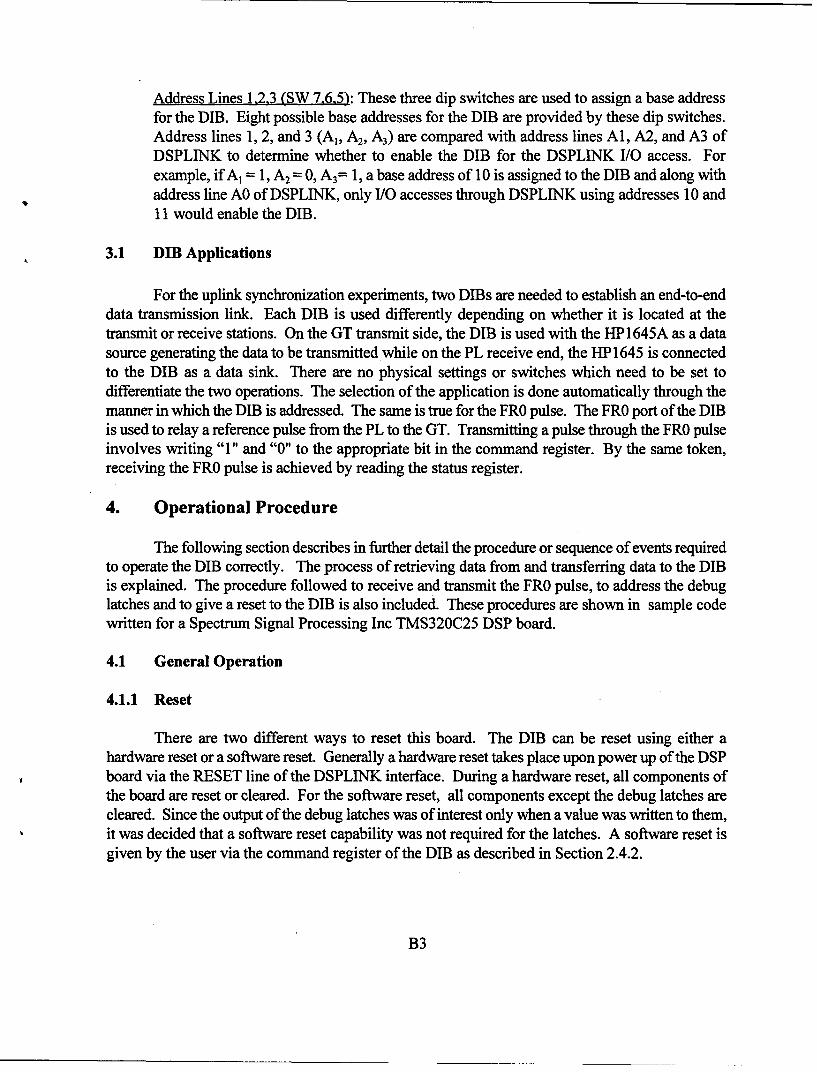
Address Lines 1.2.3 (SW 7.6.5): These three dip switches are used to assign a base addressfor the DIB. Eight possible base addresses for the DIB are provided by these dip switches.Address lines 1, 2, and 3 (A,, A2, A3) are compared with address lines Al, A2, and A3 ofDSPLINK to determine whether to enable the DIB for the DSPLINK I/O access. Forexample, if A1 = 1, A 2 = 0, A 3= 1, a base address of 10 is assigned to the DIB and along withaddress line AO of DSPLINK, only I/O accesses through DSPLINK using addresses 10 and11 would enable the DIB.
3.1 DIB Applications
For the uplink synchronization experiments, two DIBs are needed to establish an end-to-enddata transmission link. Each DIB is used differently depending on whether it is located at thetransmit or receive stations. On the GT transmit side, the DIB is used with the HP 1 645A as a datasource generating the data to be transmitted while on the PL receive end, the HP 1645 is connectedto the DIB as a data sink. There are no physical settings or switches which need to be set todifferentiate the two operations. The selection of the application is done automatically through themanner in which the DIB is addressed. The same is true for the FRO pulse. The FRO port of the DIBis used to relay a reference pulse from the PL to the GT. Transmitting a pulse through the FRO pulseinvolves writing "1" and "0" to the appropriate bit in the command register. By the same token,receiving the FRO pulse is achieved by reading the status register.
4. Operational Procedure
The following section describes in further detail the procedure or sequence of events requiredto operate the DIB correctly. The process of retrieving data from and transferring data to the DIBis explained. The procedure followed to receive and transmit the FRO pulse, to address the debuglatches and to give a reset to the DIB is also included. These procedures are shown in sample codewritten for a Spectrum Signal Processing Inc TMS320C25 DSP board.
4.1 General Operation
4.1.1 Reset
There are two different ways to reset this board. The DIB can be reset using either ahardware reset or a software reset. Generally a hardware reset takes place upon power up of the DSPboard via the RESET line of the DSPLINK interface. During a hardware reset, all components ofthe board are reset or cleared. For the software reset, all components except the debug latches arecleared. Since the output of the debug latches was of interest only when a value was written to them,it was decided that a software reset capability was not required for the latches. A software reset isgiven by the user via the command register of the DIB as described in Section 2.4.2.
B3

The software reset pulse for the DIB is an active-high signal. In order to generate a softwarereset pulse for the DIB the user must first write a "l" to bit 15 of the command register. The DIBcircuitry will then generate the appropriate "high" or "low" signal for the various components on theboard. After the reset occurs, the command register must be returned to its initial state (i.e. the resetmust be cleared). The user must write a "0" to bit 15 of the command register to clear the reset line.
The following is sample code written for the TMS320c25 DSP board to perform software reset ofthe DIB:
BOARD .set 0 ;base address of DIB - 0
COMMND .set BOARD+l ;COMMAND port address
RESHI .set 8000h ;Set reset bit (D15) to "high" commandRESLO .set Oh ;Clear reset bit command
; Sample code begins here
OUT RESHI,COMMND ;send a "l" to D15NOPNOPNOPOUT RESLO,COMMND ;send a "0" to D15,clear reset
; End of sample code
4.1.2 Selecting the destination for the data transferred to the DIB
The process of transferring data to either the data buffer or one of the debug latches involvestwo steps as described in Section 2.4.2. First the user must select the destination which isrepresented by DO and D1 of the command register. To select the destination, DO and DI of thecommand register must be set to one of the values defined in Table B2. Thus, for normal operationof the DIB, bits DO and D1 should always be set to '0'.
Command Register Destination selected
D1/D0 value I
00 Data buffer
01 Debug Latch #1
10 Debug Latch #2
11 Debug Latch #3
Table B2. Settings for selecting destination of data transfer to DIB
The following sample code for the TMS320C25 DSP would be used to select debug latch #1 asthe destination of the data transfer:
B4

BOARD .set 0 ;base address of DIB = 0
COMMND .set BOARD+l ;COMMAND port address
SELLATi .set 1 ;select debug latch #1
; Sample code begins here
OUT SELLAT1,COMMND
; End of sample code
The procedure for transferring data after the destination is selected is described further in the nextsection.
4.2 Data Operation
4.2.1 Read Data Example
The following paragraphs describe the procedure for reading data from the data buffer ofthe DIB. It is assumed that the board has a base address of '0' (i.e. Al, A2, A3 = '0') and theread operation is continuous. For a read operation, the setting of bits DO and Dl of the commandregister is not necessary. However, it is assumed that DO and Dl are set to the default setting(00) for normal operation. During a read operation, single bit stream data which has beenconverted from a RS232 to TTL levels and formatted into a 12-bit word is transferred to theDSP.
The procedure for a read operation is as follows: Test and wait for bit #15 (RXRDY) ofthe status register to be set to '1'. When the RXRDY bit is set to '1', read the 12 data bits fromthe DIB buffer. Reading the data clears the RXRDY flag. The data occupies the lower 12 bits ofthe 16 data lines on DSPLINK. If the data is not read before the next 12 bits are available fromthe data source, the RXOVR bit is set to a '1' meaning that an error has occurred.
A sample code for the read operation written for the TMS320C25 DSP follows:
BOARD .set 0 ;base address of DIB = 0
RXDATA .set BOARD+0 ;Read DATA port addressRDSTAT .set BOARD+l ;Read STATUS port address
RXRDY .set Oh ;C25 bit code for receive ready status bit, D15
.bss STAT ;status register variable
.bss HOLD ;data buffer variable
Sample code begins here
RD LOOP:
WAITRDY:IN STAT,RDSTAT ;read DIB status registerBIT STAT,RXRDY ;test bit 15BBZ WAITRDY ;keep waiting if bit not set
RDDATA:
B5
IN HOLD,RXDATA ;read data from buffer into HOLD
B RDLOOP ;End of loop
End of sample code
4.2.2 Send Data Example
The procedure for sending data to the DIB is similar to reading data from the DIB.Again, it is assumed that the board has a base address of '0' (i.e. A ,, A2, A3 = '0'). It is alsoassumed that the data is to be transferred to the data buffer. As a result, the command registerbits DO and D1 must be set to '0' prior to the data transfer (see Section 4.1.1 of this appendix).During a send operation, 12-bit words are transferred to the DIB from the DSP and formattedinto a single data bit stream. The bit stream is converted from TTL to RS232 levels and thentransferred to the data device.
The procedure for a send operation is as follows: Test and wait for bit #13 (TXMT) of thestatus register to be set to '1'. When the TXMT bit is set to '1', transfer the data to the databuffer. Sending the data clears the TXMT flag. The data is transferred in the lower 12 bits of the16 data lines on DSPLINK. If the data is not sent, the TXUND bit is set to a '1' meaning that anerror has occurred.
BOARD .set 0 ;base address of DIB = 0
TXDATA .set BOARD+O ;Read DATA port addressRDSTAT .set BOARD+I ;Read STATUS port addressCOMMND .set BOARD+I ;Command port address
TXMT .set 2h ;C25 bit code for transmit empty status bit, D13
SELBUFF .set 0 ;select data buffer
DATA .set 99 ;Arbitrary data value to be transferred
.bss STAT,1 ;status register variable
Sample code begins here
TXLOOP:
WAITMT:IN STAT,RDSTAT ;read DIB status registerBIT STAT,TXMT ;test bit 13BBZ WAITMT ;keep waiting if bit not set
SENDDATA:OUT SELBUFF,COMMND;select destination to be data bufferNOPOUT DATA,TXDATA ;transfer data to DIB
B TX_LOOP ;End of loop
End of sample code
B6

4.2.3 Writing to Debug Latches
In cases where a user would like to verify the value of a register, for example, it ispossible to write the value to one of three debug latches on the DIB. The procedure for writingdata to a debug latch mirrors that of writing to the data buffer. The difference comes from theselection of the destination in bits DO and Dl of the command register as discussed above. Oncethe data transfer to the latch is complete, the command register is set back to its default so thatthe data buffer is selected as the destination. For this example, it is assumed that the board has abase address of '0'. It is also important to mention that there are three debug latches on the DIB,but only one (#1) is brought out on a connector (26-pin) to the front panel. A user can write datato a latch anytime during the program.
The procedure for writing data to a debug latch is as follows: The user sets the commandregister to address the specific debug latch (bit 0,1) according to Table B2. Then, the data is sentto the latch using the TXDATA command in the program. Finally, the command register isreturned to its initial state (zero) in order for the program to continue with the normal path of thedata.
Sample code is provided below to transfer a data value to debug latch #1.
BOARD .set 0 ;base address of DIB = 0
TXDATA .set BOARD+O ;Read DATA port addressCOMMND .set BOARD+l ;Command port address
SELBUFF .set 0 ;select data buffer as destinationSELLATi .set 1 ;select debug latch #1 as destination
DATA .set 99 ;Arbitrary data value to be transferred
; Sample code begins here
SEND DATA:OUT SELLATl,COMMND;select destination to be debug latch #1NOPOUT DATA, TXDATA ;transfer data to debug latchNOPOUT SELBUFF,COMMND;select destination to be data buffer
End of sample code
4.2.4 Frame Zero Pulse
For the uplink synchronization experiment, a downlink synchronization reference seriallink is implemented to transmit an estimate of the payload clock to the ground terminal in orderto begin the process of uplink synchronization. The estimate is transmitted in the form of apulse. The rising edges and falling edges refer to specific times in the PL system hop sequence.The DIB provides the interface between the simulators and the serial link for both the generationand detection of the FRO pulse.
B7
To generate the rising edge of the pulse, the FROout bit (bit 2) of the command registeris set to '1' (default is '0'). For the falling edge, the FROout bit is returned to '0'. For the uplinksynchronization experiments, the PL continuously generates this reference pulse for the GT touse for syncrhonization.
To receive the FRO pulse, a user repeatedly reads the status register and monitors bit D1I(FROin) of the status register. The GT processor adjusts its clock based on the detection of therising and falling edges of the pulse. For the uplink synchronization experiments, the rising edgeof the FRO pulse corresponds to the zeroth hop of the zeroth frame in the hop sequence. Thefalling edge of the FRO pulse corresponds to the zeroth hop of the first frame.
The sample TMS320C25 DSP code provided directly below illustrates the procedure fortransmitting one FRO pulse.
BOARD .set 0 ;base address of DIB = 0
COMMND .set BOARD+l ;COMMAND port address
FRMO HI .set 4 ;set D2 of COMMAND reg to 'I1FRM0--LO .set 0 ;clear D2 of COMMAND reg
; Sample code begins here; It is assumed that the FRO bit is originally set to be 0 (default)
OUT FRMOHI,COMMND ;put a I'' on FRO bit of COMMAND regNOP ;delayNOPNOPNOPNOPNOPOUT FRMOLO,COMMND ;put 101 on FRO bit of COMMAND reg
; End of sample code
The sample code written for the TMS320C25 DSP board for detecting the FRO pulse is asfollows:
BOARD .set 0 ;base address of DIB = 0
RDSTAT .set BOARD+l ;Read STATUS port address
FRMO_RX .set 4h ;C25 bit code for FRO bit on status reg (DlI)
.bss STAT,1
Sample code begins here
DET FR0O:IN STAT,RDSTAT ;read status register of DIBBIT FRMO RX, STAT ;test bit D11CALL CHK_4_EDGE ;call subroutine to check for fall/ris edge
;(not included here)
B8

Appendix C: Test Program for DIB
1. General
This appendix contains the listings of the program used by the PC (station) to test the DIBaccording to Fig. 7 of the main document. The testing steps are briefly described in section 4 ofthis document. There will be comments after the program codes when needed to explain themeaning of that particular code.
2. Program Listings
The program listings for the testing of the DIB are found in the following pages.
2.1 C Listing (Berhost). User interface program for a PC.2.2 Assembler listing (Bertest). DSP assembler program.2.3 Berhost.MAK. To compile and link C program.2.4 Bertest.MAK. To compile and link assembler program.2.5 Bertest.CMD. Linker file used to produce output file to be loaded into DSP memory.
C1

2.1 C Listing
Berhost.C
#include <stdlib.h>#include <conio.h>#include <stdio.h>#include "TIC25.h" /* TMS320 development Lib. header file. */
#define PROCBD 3 /* Corresponds to I/O ports 390-397 */
#define MAXWAIT 50000L#define TIMWAIT 2000L
#define CLEAR 0#define TBEGIN 1#define TSTAT 2#define TRESLT 3#define TDEMOD 4
#define C251N 0#define C25PI 1#define C25P2 2#define C25P3 3#define PCIN 4#define PCP1 5#define PCP2 6#define PCP3 7#define FRO FLG 8#define DEBUG 9
ushort mail base;int stop-flag = 0;
void init board(int board);void sendandwait(ushort type,ushort pl,ushort p2,ushort p3,1ong count);ushort get mail(ushort *pl,ushort *p2,ushort *p3,long count);ushort mread(ushort addr);void mwrite(ushort addr,ushort val);void checkkey(void);void display_mail(ushort type,ushort pl,ushort p2,ushort p3);
void main(){ushort ans,tl,t2,t3,mtype;long i,j;
initboard(PROCBD);send and wait(TBEGIN,0,0,0,MAXWAIT);exit(0);
C2
void init-board(int board)
int loadstatus;
SelectBoard (board);AssertReset 0;UnHoldo;RemoveFlag 0;CommRWDisO;CommRRflis();
A ReadStatRego;ReadStatReg();loadstatus = LoadObjectFile("lbertest.out"l);if (loadstatus != 0) {printf("Error! Not able to load \bertest.out\ down to the board\n");
exit (1);
RelReseto;WaitComWr (MAXWAIT);mail -base = RdCommRego;return;
void send-and-wait (ushort type,ushort pl,ushort p2,ushort p3,long count)
long i,j;
mwrite (C2 5P1, pl);mwrite(C25P2,p2);mwrite(C25P3,p3);mwrite(C251N,type);mwrite(DEBUG,l);
for (j=O;j<2000;j++){for (i0O;i<500;i++){
/ *nothing* /
mwrite(FROFLG,0);for (i=l;i.<500;i++){
/*nothing* /
mwrite(FROFLG,1);
mwrite(DEBUG,0);return;
C3

ushort get mail (ushort *pl,ushort *p2,ushort *p3,long count)
long i;ushort mtype;if (count != 0){
for (i=o;i.~count;i++) if ((mtype=mread(PCIN)) 1= CLEAR) break;if Ui= count) return CLEAR;
}else(while ((mtype=mread(PCIN)) ==CLEAR);
*} radPP)*pl = mread(PCP2);*3= mread(PCP3);
mwrite (PCIN, CLEAR);return mtype;
ushort mread(ushort addr)
return GetMeml6 ( DIn,addr+mail-base);
void mwrite(ushort addr,ushort val)
PutMeml6('D' ,addr+mail base,val);return;
void checkkey (void)
mnt c;
if (kbhit()o 0) return;c= getch();switch (c){
case 'q':case IQ':case 1x':
case 'K':case 'el:case 'E':case 1\033':
stop-flag =1;
break;case 0:
c = getcho;break;
default:break;
return;}
C4

void display mail (ushort type,ushort pl,ushort p2,ushort p3)
char buff [80);
switch (type){case CLEAR:
printf("No message - timeout\n");break;
case TEEGIN:printf ("Illegal BEGIN message\n");break;
case TSTAT:itoaC (long) pl,buff,2);printf ("STATUS %16s (%-X)\n"',buff,pl);break;
case TRESLT:ltoa((long) pl,buff,2);printf(", Res = %12s (%x)\n",buff,pl);break;
case TDEMOD:ltoa((long) pl,buff,2);printf("'Demod = 12s (%X)\n"1,buff,pl);break;
default:printf("Illegal message type %d (%d, %d, %d)\n"',type,p1,p2,p3);break;
return;
C5

2.2 Assembler Listing
Bertest.ASM
.global MAIN
.global RESET,INTO,INTIINT2,TINT,RINT,XINT,USER,BADINT
PORTO: .set 0
BOARD: .set 8RXDATA: .set BOARD + 0 ; Receive data (read only)TXDATA: .set BOARD + 0 ; Transmit data (write only)SFLAGS: •set BOARD + 1 ; Status flags (read only)HOPEDG: .set 15 ; C25 bit code for Bit position 0 (LSB)FIFOMT: .set 14 ; C25 bit code for Bit position 1FRMZERO: .set 4 ; C25 bit code for Bit position 11TXUND: .set 3 ; C25 bit code for Bit position 12TXMT: .set 2 ; C25 bit code for Bit position 13RXOVR: .set 1 ; C25 bit code for Bit position 14RXRDY: .set 0 ; C25 bit code for Bit position 15 (MSB)COMMND: .set BOARD + 1 ; Command - used for reset (write only)ADDATA: .set BOARD + 2 ; A/D FIFO data (read only)
CLEAR: .set 0TBEGIN: .set 1TSTAT: .set 2TRESLT: .set 3TDEMOD: .set 4
.sect "IRUPTS"RESET: B MAININTO: B BADINTINTI: B BADINTINT2: B BADINT
.space 16 * 16TINT: B BADINTRINT: B BADINTXINT: B BADINTUSER: B BADINT
.sect "IniDat"MAILBAS:C25IN: .word CLEARC25PI: .word 0C25P2: .word 0C25P3: .word 0PCIN: .word CLEARPCPl: .word 0
C6

PCP2: .word 0PCP3: .word 0FROFLG .word 0DEBUG .word 0
TMPIN: .word 0TMPP1: .word 0TMPP2: .word 0TMPP3: .word 0
XOLD: .word 0YOLD: .word 0X: .word 0Y: .word 0
STAT: .word 0HOLD: .word 0FLAG: .word 0TEMP: .word 0CO: .word 0
UN: .word 1DEUX: .word 2TROIS: .word 3FRM 0: .word 4QZ: .word 8000hNUM word OAAAAh
.text
BADINT:SXF
BADLOP: B BADLOP
Main Program
MAIN:DINT ; Ensure interrupts disabledROVM ; Reset overflow maskLARP ARI ; Set ARP to AROLDPK 0 ; Point to page 0 (control area)LACK 0 ; Mask off all interruptsSACL 4RSXM ; Disable sign extensionSPM 0 ; No shift on P register
C7
LDPK MAILBAS ; Point to data area
LALK MAILBAS ; Send mail base address to PCSACL TEMPOUT TEMP,PORTOLALK 0
SACL FLAG
WAITBG:CALL WAITM ; Waits for FLAG to begin programSUBK TBEGINBNZ WAITBG
LOOP:LAC FRO FLG ; Checks for FRM 0 and makes itBNZ CONT ; vary for testing purpose (simulate)
OUT FRM_0,COMMNDB CONT2
CONTl:OUT CO, COMMND
CONT2:IN STAT, SFLAGS ; Receives status bits from the BIB
LAC FLAGBNZ LlBIT STAT,RXRDY ; Checks for the RXready status bitBBZ Ll ; If the bit is at '0' go to LlIN HOLD,RXDATA ;stores data from BIB in HOLD
LALK 1SACL FLAG
B LOOP
Ll:
LAC FLAGBZ L2BIT STAT,TXMT ; Checks for the RX ready status bitBBZ L2 ; If the bit is at '0' go to L2NOPOUT HOLD,TXDATA ; send data in HOLD to the BIBLALK 0SACL FLAG
LAC DEBUGBZ LOOPOUT UN, COMMND ; Adresses Debug latche #1
OUT HOLD,TXDATA ; Puts the content of HOLD on latchOUT C0,COMMND ; Back to initial stateB LOOP
C8

L2:
B LOOP
_______WAIT BEGIN____
WAITM:LAC C251N
BZ WAITM
SACL TMPIN
LAC C25P1
SACL TMPP1
LAC C25P2
SACL TMPP2
LAC C25P3
SACL TMPP3LALI( CLEAR
SACL C251N
LAC TMPIN
RET.end
2.3 Berhost.MLAK
berhost exe: berhost .obj
link berhost,. , sti25dev;
berhost.obj: berhost.cci /c /Qd berhost.c
2.4 Bertest.MLAK
BERTEST.OUT: BERTEST. OBJ
C: \tms\DSPLNK BERTEST. CID
BERTEST. OBJ: BERTEST .ASM
C:\tms\DSPA BERTEST.ASM -1
2.5 Bertest.CMD
BERTEST.OBJ 1* BER Board Test Software *
-e MAIN /* Entry point
-o BERTEST.OUT /* Executable file *-m BERTEST.MAP 1* Map file
C9

MEMORY{PAGE 0: VECTORS: origin = OH, length = 03FH
PROG: origin = 400H, length = 01COOH
PAGE 1: DATA: origin = 8000H, length = 02000H}
SECTIONS{IRUPTS: { }> VECTORS PAGE 0.text: { } > PROG PAGE 0.data: { } > PROG PAGE 0IniDat: { } > DATA PAGE 1.bss: { } > DATA PAGE 1C
C]0

69
UNCLASSIFIEDSECURITY CLASSIFICATION OF FORM
(highest classification of Title, Abstract, Keywords)
DOCUMENT CONTROL DATA(Security classification of title, body of abstract and indexing annotation must be entered when the overall document is classified)
1. ORIGINATOR (the name and address of the organization preparing the document. 2. SECURITY CLASSIFICATIONOrganizations for whom the document was prepared, e.g. Establishment sponsoring (overall security classification of the documenta contractor's report, or tasking agency, are entered in section 8.) including special warning terms if applicable)
Defence Research Establishment OttawaOttawa, Ontario UNCLASSIFIEDK1A OZ4
3. TITLE (the complete document title as indicated on the title page. Its classification should be indicated by the appropriateabbreviation (S,C or U) in parentheses after the title.)
Multipurpose Data Interface Board (DIB) (U)
4. AUTHORS (Last name, first name, middle initial)
Simoneau (Capt), Yves and Tom, Caroline
S. DATE OF PUBLICATION (month and year of publication of 6a. NO. OF PAGES (total 6b. NO. OF REFS (total cited indocument) containing information. Include document)
July 1998 Annexes, Appendices, etc.)84 6
7. DESCRIPTIVE NOTES (the category of the document, e.g. technical report, technical note or memorandum. If appropriate, enter the type ofreport, e.g. interim, progress, summary, annual or final. Give the inclusive dates when a specific reporting period is covered.
DREO Report
8. SPONSORING ACTIVITY (the name of the department project office or laboratory sponsoring the research and development. Include theaddress.
5cal I
9a. PROJECT OR GRANT NO. (if appropriate, the applicable research 9b. CONTRACT NO. (if appropriate, the applicable number underand development project or grant number under which the document which the document was written)was written. Please specify whether project or grant)
10a. ORIGINATOR'S DOCUMENT NUMBER (the official document 10b. OTHER DOCUMENT NOS. (Any other numbers which maynumber by which the document is identified by the originating be assigned this document either by the originator or by theactivity. This number must be unique to this document.) sponsor)
DREO REPORT 1332
11. DOCUMENT AVAILABILITY (any limitations on further dissemination of the document, other than those imposed by security classification)
(X) Unlimited distribution( ) Distribution limited to defence departments and defence contractors; further distribution only as approved( ) Distribution limited to defence departments and Canadian defence contractors; further distribution only as approved( ) Distribution limited to government departments and agencies; further distribution only as approved
) Distribution limited to defence departments; further distribution only as approved) Other (please specify):
12. DOCUMENT ANNOUNCEMENT (any limitation to the bibliographic announcement of this document. This will normally correspond to
the Document Availability (11). however, where further distribution (beyond the audience specified in 11) is possible, a widerannouncement audience may be selected.)
Unlimited Announcement
UNCLASSIFIEDSECURITY CLASSIFICATION OF FORM RA.W (21 Dec 92)

70
UNCLASSIFIEDSECURITY CLASSIFICATION OF FORM
13. ABSTRACT (a brief and factual summary of the document. It may also appear elsewhere in the body of the document itself. It is highlydesirable that the abstract of classified documents be unclassified. Each paragraph of the abstract shall begin with an indication of thesecurity classification of the information in the paragraph (unless the document itself is unclassified) represented as (S), (C), or (U).It is not necessary to include here abstracts in both official languages unless the text is bilingual).
Defence Research Establishment Ottawa is pursuing an in-house researchactivity in spread-sprectrum technology to support development of robust,anti-jam satellite communications for the military. The in-house effortconsists of developing a system simulator, including both a ground terminalprocessor and a payload processor, to research techniques involved inspread-spectrum synchronization. For these experiments, a multipurposedata interface board is required for different data operations, and is thesubject of this report. The board is composed of mainly an erasableprogrammable logic device to reduce the number of integrated circuitsand to add flexibility to the design. The board was designed to performthree functions. The first function is the data format conversion betweena ground terminal processor and a data source, and likewise, a payloadprocessor and a data sink. The second function is to provide an interfaceto a separate direct link between the payload and ground terminalsubsystems for transmitting a reference pulse for synchronization. Thethird function is to provide a set of debug latches for the user. Inthis document, the software and hardware details are provided along witha user's guide for the board.
14. KEYWORDS, DESCRIPTORS or IDENTIFIERS (technically meaningful terms or short phrases that characterize a document and could behelpful in cataloguing the document. They should be selected so that no security classification is required. Identifiers, such as equipmentmodel designation, trade name, military project code name, geographic location may also be included. If possible keywords should be selectedfrom a published thesaurus. e.g. Thesaurus of Engineering and Scientific Terms (TEST) and that thesaurus-identified. If it is not possible toselect indexing terms which are Unclassified, the classification of each should be indicated as with the title.)
data format conversiondata interface boarderasable programmable logic deviceEPLD
UNCLASSIFIEDSECURITY CLASSIFICATION OF FORM