multichannel codec with s/pdif transceiver€¦ · · 2016-12-16multichannel codec with s/pdif...
TRANSCRIPT
w WM8580A
Multichannel CODEC with S/PDIF Transceiver
WOLFSON MICROELECTRONICS plc
Production Data, November 2013, Rev 4.9
Copyright 2013 Wolfson Microelectronics plc
DESCRIPTION
The WM8580A is a multi-channel audio CODEC with S/PDIF transceiver. The WM8580A is ideal for DVD and surround sound processing applications for home hi-fi, automotive and other audiovisual equipment.
Integrated into the device is a stereo 24-bit multi-bit sigma delta ADC with support for digital audio output word lengths from 16-bit to 32-bit, and sampling rates from 8kHz to 192kHz.
Also included are three stereo 24-bit multi-bit sigma delta DACs, each with a dedicated oversampling digital interpolation filter. Digital audio input word lengths from 16-bits to 32-bits and sampling rates from 8kHz to 192kHz are supported. Each DAC channel has independent digital volume and mute control.
Two independent audio data interfaces support I2S, Left Justified, Right Justified and DSP digital audio formats. Each audio interface can operate in either Master Mode or Slave Mode.
The S/PDIF transceiver is IEC-60958-3 compatible and supports frame rates from 32k/s to 96k/s. It has four multiplexed inputs and one output. Status and error monitoring is built-in and results can reported over the serial interface or via GPO pins. S/PDIF Channel Block configuration is also supported.
The device has two PLLs that can be configured independently to generate two system clocks for internal or external use.
Device control and setup is via a 2-wire or 3-wire (SPI compatible) serial interface. The serial interface provides access to all features including channel selection, volume controls, mutes, de-emphasis, S/PDIF control/status, and power management facilities. Alternatively, the device has a Hardware Control Mode where device features can be enabled/disabled using selected pins.
The device is available in a 48-lead TQFP package.
FEATURES Multi-channel CODEC with 3 Stereo DACs and 1 Stereo
ADC
Integrated S/PDIF / IEC-60958-3 transceiver
Audio Performance
103dB SNR (‘A’ weighted @ 48kHz) DAC
-90dB THD (48kHz) DAC
100dB SNR (‘A’ weighted @ 48kHz) ADC
-87dB THD (48kHz) ADC
DAC Sampling Frequency: 8kHz – 192kHz
ADC Sampling Frequency: 8kHz – 192kHz
Independent ADC and DAC Sample Rates
2 and 3-Wire Serial Control Interface with readback, or Hardware Control Interface
GPO pins allow visibility of user selected status flags
Programmable Audio Data Interface Modes
I2S, Left, Right Justified or DSP
16/20/24/32 bit Word Lengths
Three Independent Stereo DAC Outputs with Digital Volume Controls
Two Independent Master or Slave Audio Data Interfaces
Flexible Digital Interface Routing with Clock Selection Control
2.7V to 5.5V Analogue, 2.7V to 3.6V Digital Supply Operation
48-lead TQFP Package
APPLICATIONS Digital TV DVD Players and Receivers Surround Sound AV Processors and Hi-Fi systems Automotive Audio
WM8580A Production Data
w PD, Rev 4.9, November 2013
2
BLOCK DIAGRAM
Production Data WM8580A
w PD, Rev 4.9, November 2013
3
TABLE OF CONTENTS
DESCRIPTION ....................................................................................................... 1 FEATURES ............................................................................................................ 1 APPLICATIONS ..................................................................................................... 1 BLOCK DIAGRAM ................................................................................................ 2 TABLE OF CONTENTS ......................................................................................... 3 PIN CONFIGURATION .......................................................................................... 4 ORDERING INFORMATION .................................................................................. 4 PIN DESCRIPTION ................................................................................................ 5
MULTI-FUNCTION PINS ................................................................................................. 6 ABSOLUTE MAXIMUM RATINGS ........................................................................ 8 RECOMMENDED OPERATING CONDITIONS ..................................................... 9 ELECTRICAL CHARACTERISTICS ..................................................................... 9
TERMINOLOGY ............................................................................................................ 12 MASTER CLOCK TIMING ............................................................................................. 12 DIGITAL AUDIO INTERFACE – MASTER MODE ........................................................ 13 DIGITAL AUDIO INTERFACE – SLAVE MODE ............................................................ 14 CONTROL INTERFACE TIMING – 3-WIRE MODE ...................................................... 15 CONTROL INTERFACE TIMING – 2-WIRE MODE ...................................................... 16
DEVICE DESCRIPTION ...................................................................................... 17 INTRODUCTION ........................................................................................................... 17 CONTROL INTERFACE OPERATION .......................................................................... 18 DIGITAL AUDIO INTERFACES ..................................................................................... 22 AUDIO DATA FORMATS .............................................................................................. 24 AUDIO INTERFACE CONTROL ................................................................................... 28 DAC FEATURES ........................................................................................................... 30 ADC FEATURES ........................................................................................................... 39 DIGITAL ROUTING OPTIONS ...................................................................................... 40 CLOCK SELECTION ..................................................................................................... 42 PHASE-LOCKED LOOPS AND S/PDIF CLOCKING (SOFTWARE MODE) ................. 53 PHASE-LOCKED LOOPS AND S/PDIF CLOCKING (HARDWARE MODE) ................ 60 S/PDIF TRANSCEIVER ................................................................................................. 60 POWERDOWN MODES ................................................................................................ 73 INTERNAL POWER ON RESET CIRCUIT .................................................................... 75 HARDWARE CONTROL MODE.................................................................................... 77 REGISTER MAP ............................................................................................................ 81
DIGITAL FILTER CHARACTERISTICS .............................................................. 97 DAC FILTER RESPONSES .......................................................................................... 98 DIGITAL DE-EMPHASIS CHARACTERISTICS ............................................................ 99 ADC FILTER RESPONSES .......................................................................................... 99 ADC HIGH PASS FILTER ........................................................................................... 100
APPLICATIONS INFORMATION ...................................................................... 101 RECOMMENDED EXTERNAL COMPONENTS ......................................................... 101
PACKAGE DIMENSIONS .................................................................................. 103 IMPORTANT NOTICE ....................................................................................... 104
ADDRESS: .................................................................................................................. 104
WM8580A Production Data
w PD, Rev 4.9, November 2013
4
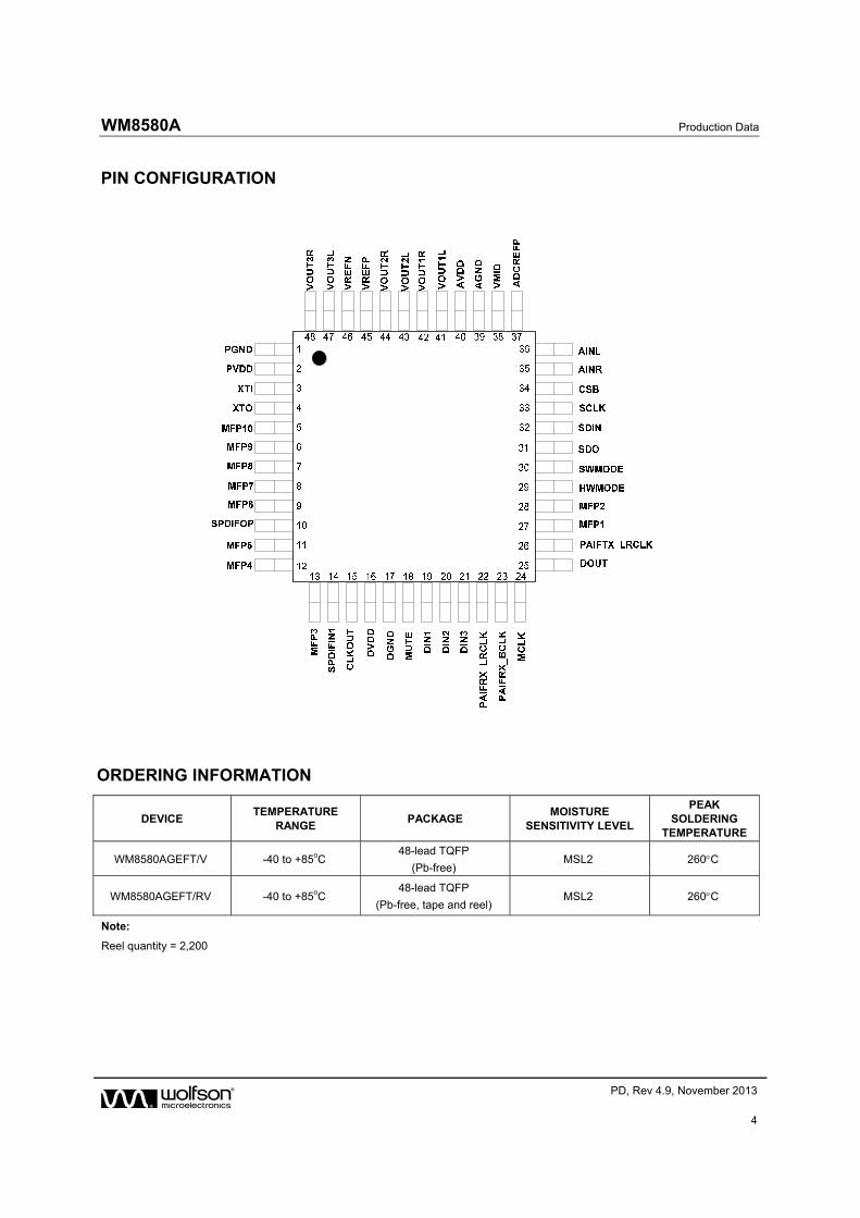
PIN CONFIGURATION
ORDERING INFORMATION
DEVICE TEMPERATURE
RANGE PACKAGE
MOISTURE SENSITIVITY LEVEL
PEAK SOLDERING
TEMPERATURE
WM8580AGEFT/V -40 to +85oC 48-lead TQFP
(Pb-free) MSL2 260C
WM8580AGEFT/RV -40 to +85oC 48-lead TQFP
(Pb-free, tape and reel) MSL2 260C
Note:
Reel quantity = 2,200
Production Data WM8580A
w PD, Rev 4.9, November 2013
5
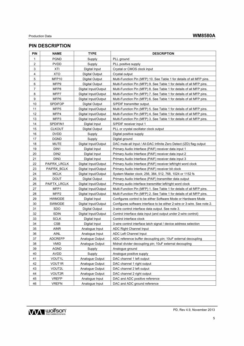
PIN DESCRIPTION
PIN NAME TYPE DESCRIPTION
1 PGND Supply PLL ground
2 PVDD Supply PLL positive supply
3 XTI Digital Input Crystal or CMOS clock input
4 XTO Digital Output Crystal output
5 MFP10 Digital Output Multi-Function Pin (MFP) 10. See Table 1 for details of all MFP pins.
6 MFP9 Digital Output Multi-Function Pin (MFP) 9. See Table 1 for details of all MFP pins.
7 MFP8 Digital Input/Output Multi-Function Pin (MFP) 8. See Table 1 for details of all MFP pins.
8 MFP7 Digital Input/Output Multi-Function Pin (MFP) 7. See Table 1 for details of all MFP pins.
9 MFP6 Digital Input/Output Multi-Function Pin (MFP) 6. See Table 1 for details of all MFP pins.
10 SPDIFOP Digital Output S/PDIF transmitter output.
11 MFP5 Digital Input/Output Multi-Function Pin (MFP) 5. See Table 1 for details of all MFP pins.
12 MFP4 Digital Input/Output Multi-Function Pin (MFP) 4. See Table 1 for details of all MFP pins.
13 MFP3 Digital Input/Output Multi-Function Pin (MFP) 3. See Table 1 for details of all MFP pins.
14 SPDIFIN1 Digital Input S/PDIF receiver input 1
15 CLKOUT Digital Output PLL or crystal oscillator clock output
16 DVDD Supply Digital positive supply
17 DGND Supply Digital ground
18 MUTE Digital Input/Output DAC mute-all Input / All-DAC Infinite Zero Detect (IZD) flag output
19 DIN1 Digital Input Primary Audio Interface (PAIF) receiver data input 1
20 DIN2 Digital Input Primary Audio Interface (PAIF) receiver data input 2
21 DIN3 Digital Input Primary Audio Interface (PAIF) receiver data input 3
22 PAIFRX_LRCLK Digital Input/Output Primary Audio Interface (PAIF) receiver left/right word clock
23 PAIFRX_BCLK Digital Input/Output Primary Audio Interface (PAIF) receiver bit clock
24 MCLK Digital Input/Output System Master clock; 256, 384, 512, 768, 1024 or 1152 fs
25 DOUT Digital Output Primary Audio Interface (PAIF) transmitter data output
26 PAIFTX_LRCLK Digital Input/Output Primary audio interface transmitter left/right word clock
27 MFP1 Digital Input/Output Multi-Function Pin (MFP) 1. See Table 1 for details of all MFP pins.
28 MFP2 Digital Input/Output Multi-Function Pin (MFP) 2. See Table 1 for details of all MFP pins.
29 HWMODE Digital Input Configures control to be either Software Mode or Hardware Mode
30 SWMODE Digital Input/Output Configures software interface to be either 2-wire or 3-wire. See note 2.
31 SDO Digital Output 3-wire control interface data output. See note 3.
32 SDIN Digital Input/Output Control interface data input (and output under 2-wire control)
33 SCLK Digital Input Control interface clock
34 CSB Digital Input 3-wire control interface latch signal / device address selection
35 AINR Analogue Input ADC Right Channel Input
36 AINL Analogue Input ADC Left Channel Input
37 ADCREFP Analogue Output ADC reference buffer decoupling pin; 10uF external decoupling
38 VMID Analogue Output Midrail divider decoupling pin; 10uF external decoupling
39 AGND Supply Analogue ground
40 AVDD Supply Analogue positive supply
41 VOUT1L Analogue Output DAC channel 1 left output
42 VOUT1R Analogue Output DAC channel 1 right output
43 VOUT2L Analogue Output DAC channel 2 left output
44 VOUT2R Analogue Output DAC channel 2 right output
45 VREFP Analogue Input DAC and ADC positive reference
46 VREFN Analogue Input DAC and ADC ground reference
WM8580A Production Data
w PD, Rev 4.9, November 2013
6
PIN NAME TYPE DESCRIPTION
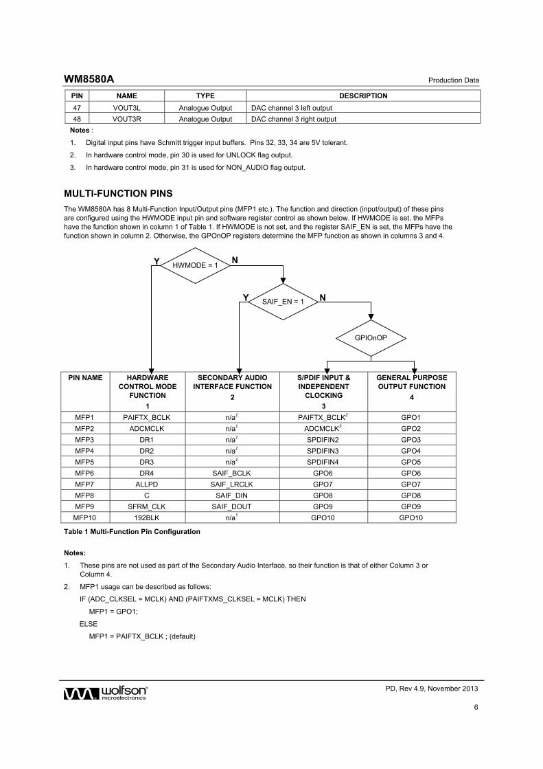
47 VOUT3L Analogue Output DAC channel 3 left output
48 VOUT3R Analogue Output DAC channel 3 right output
Notes :
1. Digital input pins have Schmitt trigger input buffers. Pins 32, 33, 34 are 5V tolerant.
2. In hardware control mode, pin 30 is used for UNLOCK flag output.
3. In hardware control mode, pin 31 is used for NON_AUDIO flag output.
MULTI-FUNCTION PINS
The WM8580A has 8 Multi-Function Input/Output pins (MFP1 etc.). The function and direction (input/output) of these pins are configured using the HWMODE input pin and software register control as shown below. If HWMODE is set, the MFPs have the function shown in column 1 of Table 1. If HWMODE is not set, and the register SAIF_EN is set, the MFPs have the function shown in column 2. Otherwise, the GPOnOP registers determine the MFP function as shown in columns 3 and 4.
PIN NAME HARDWARE CONTROL MODE
FUNCTION
1
SECONDARY AUDIO INTERFACE FUNCTION
2
S/PDIF INPUT & INDEPENDENT
CLOCKING
3
GENERAL PURPOSE OUTPUT FUNCTION
4
MFP1 PAIFTX_BCLK n/a1 PAIFTX_BCLK2 GPO1
MFP2 ADCMCLK n/a1 ADCMCLK3 GPO2
MFP3 DR1 n/a1 SPDIFIN2 GPO3
MFP4 DR2 n/a1 SPDIFIN3 GPO4
MFP5 DR3 n/a1 SPDIFIN4 GPO5
MFP6 DR4 SAIF_BCLK GPO6 GPO6
MFP7 ALLPD SAIF_LRCLK GPO7 GPO7
MFP8 C SAIF_DIN GPO8 GPO8
MFP9 SFRM_CLK SAIF_DOUT GPO9 GPO9
MFP10 192BLK n/a1 GPO10 GPO10
Table 1 Multi-Function Pin Configuration
Notes:
1. These pins are not used as part of the Secondary Audio Interface, so their function is that of either Column 3 or Column 4.
2. MFP1 usage can be described as follows:
IF (ADC_CLKSEL = MCLK) AND (PAIFTXMS_CLKSEL = MCLK) THEN
MFP1 = GPO1;
ELSE
MFP1 = PAIFTX_BCLK ; (default)
HWMODE = 1
GPIOnOP
SAIF_EN = 1
Y
Y
N
N
Production Data WM8580A
w PD, Rev 4.9, November 2013
7
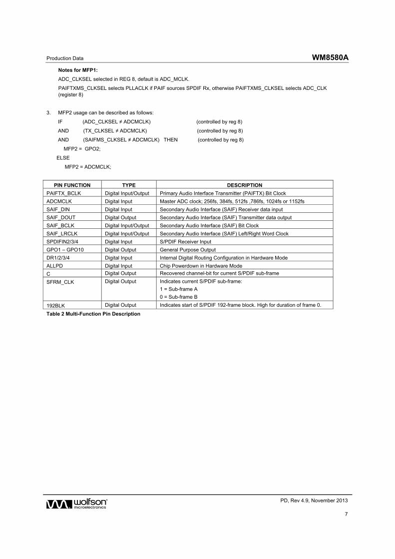
Notes for MFP1:
ADC_CLKSEL selected in REG 8, default is ADC_MCLK.
PAIFTXMS_CLKSEL selects PLLACLK if PAIF sources SPDIF Rx, otherwise PAIFTXMS_CLKSEL selects ADC_CLK (register 8)
3. MFP2 usage can be described as follows:
IF (ADC_CLKSEL ≠ ADCMCLK) (controlled by reg 8)
AND (TX_CLKSEL ≠ ADCMCLK) (controlled by reg 8)
AND (SAIFMS_CLKSEL ≠ ADCMCLK) THEN (controlled by reg 8)
MFP2 = GPO2;
ELSE
MFP2 = ADCMCLK;
PIN FUNCTION TYPE DESCRIPTION
PAIFTX_BCLK Digital Input/Output Primary Audio Interface Transmitter (PAIFTX) Bit Clock
ADCMCLK Digital Input Master ADC clock; 256fs, 384fs, 512fs ,786fs, 1024fs or 1152fs
SAIF_DIN Digital Input Secondary Audio Interface (SAIF) Receiver data input
SAIF_DOUT Digital Output Secondary Audio Interface (SAIF) Transmitter data output
SAIF_BCLK Digital Input/Output Secondary Audio Interface (SAIF) Bit Clock
SAIF_LRCLK Digital Input/Output Secondary Audio Interface (SAIF) Left/Right Word Clock
SPDIFIN2/3/4 Digital Input S/PDIF Receiver Input
GPO1 – GPO10 Digital Output General Purpose Output
DR1/2/3/4 Digital Input Internal Digital Routing Configuration in Hardware Mode
ALLPD Digital Input Chip Powerdown in Hardware Mode
C Digital Output Recovered channel-bit for current S/PDIF sub-frame
SFRM_CLK Digital Output Indicates current S/PDIF sub-frame:
1 = Sub-frame A
0 = Sub-frame B
192BLK Digital Output Indicates start of S/PDIF 192-frame block. High for duration of frame 0.
Table 2 Multi-Function Pin Description
WM8580A Production Data
w PD, Rev 4.9, November 2013
8
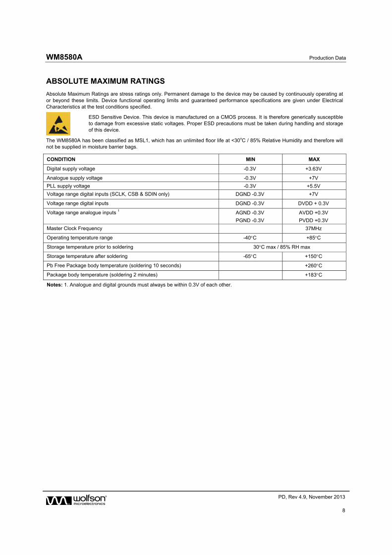
ABSOLUTE MAXIMUM RATINGS
Absolute Maximum Ratings are stress ratings only. Permanent damage to the device may be caused by continuously operating at or beyond these limits. Device functional operating limits and guaranteed performance specifications are given under Electrical Characteristics at the test conditions specified.
ESD Sensitive Device. This device is manufactured on a CMOS process. It is therefore generically susceptible to damage from excessive static voltages. Proper ESD precautions must be taken during handling and storage of this device.
The WM8580A has been classified as MSL1, which has an unlimited floor life at <30oC / 85% Relative Humidity and therefore will not be supplied in moisture barrier bags.
CONDITION MIN MAX
Digital supply voltage -0.3V +3.63V
Analogue supply voltage -0.3V +7V
PLL supply voltage -0.3V +5.5V
Voltage range digital inputs (SCLK, CSB & SDIN only) DGND -0.3V +7V
Voltage range digital inputs DGND -0.3V DVDD + 0.3V
Voltage range analogue inputs 1 AGND -0.3V
PGND -0.3V
AVDD +0.3V
PVDD +0.3V
Master Clock Frequency 37MHz
Operating temperature range -40C +85C
Storage temperature prior to soldering 30C max / 85% RH max
Storage temperature after soldering -65C +150C
Pb Free Package body temperature (soldering 10 seconds) +260C
Package body temperature (soldering 2 minutes) +183C
Notes: 1. Analogue and digital grounds must always be within 0.3V of each other.
Production Data WM8580A
w PD, Rev 4.9, November 2013
9
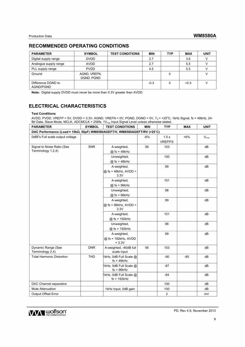
RECOMMENDED OPERATING CONDITIONS
PARAMETER SYMBOL TEST CONDITIONS MIN TYP MAX UNIT
Digital supply range DVDD 2.7 3.6 V
Analogue supply range AVDD 2.7 5.5 V
PLL supply range PVDD 4.5 5.5 V
Ground AGND, VREFN, DGND. PGND
0 V
Difference DGND to AGND/PGND
-0.3 0 +0.3 V
Note: Digital supply DVDD must never be more than 0.3V greater than AVDD.
ELECTRICAL CHARACTERISTICS
Test Conditions
AVDD, PVDD, VREFP = 5V, DVDD = 3.3V, AGND, VREFN = 0V, PGND, DGND = 0V, TA = +25oC, 1kHz Signal, fs = 48kHz, 24-Bit Data, Slave Mode, MCLK, ADCMCLK = 256fs, 1Vrms Input Signal Level unless otherwise stated.
PARAMETER SYMBOL TEST CONDITIONS MIN TYP MAX UNIT
DAC Performance (Load = 10kΩ, 50pF) WM8580AGEFT/V, WM8580AGEFT/RV (+25˚C)
0dBFs Full scale output voltage -6% 1.0 x
VREFP/5
+6% Vrms
Signal to Noise Ratio (See Terminology 1,2,4)
SNR A-weighted,
@ fs = 48kHz
95 103 dB
Unweighted,
@ fs = 48kHz
100 dB
A-weighted,
@ fs = 48kHz, AVDD = 3.3V
99 dB
A-weighted,
@ fs = 96kHz
101 dB
Unweighted,
@ fs = 96kHz
98 dB
A-weighted,
@ fs = 96kHz, AVDD = 3.3V
99 dB
A-weighted,
@ fs = 192kHz
101 dB
Unweighted,
@ fs = 192kHz
98 dB
A-weighted,
@ fs = 192kHz, AVDD = 3.3V
99 dB
Dynamic Range (See Terminology 2,4)
DNR A-weighted, -60dB full scale input
95 103 dB
Total Harmonic Distortion THD 1kHz, 0dB Full Scale @ fs = 48kHz
-90 -85 dB
1kHz, 0dB Full Scale @ fs = 96kHz
-87 dB
1kHz, 0dB Full Scale @ fs = 192kHz
-84 dB
DAC Channel separation 100 dB
Mute Attenuation 1kHz Input, 0dB gain 100 dB
Output Offset Error 2 mV
WM8580A Production Data
w PD, Rev 4.9, November 2013
10
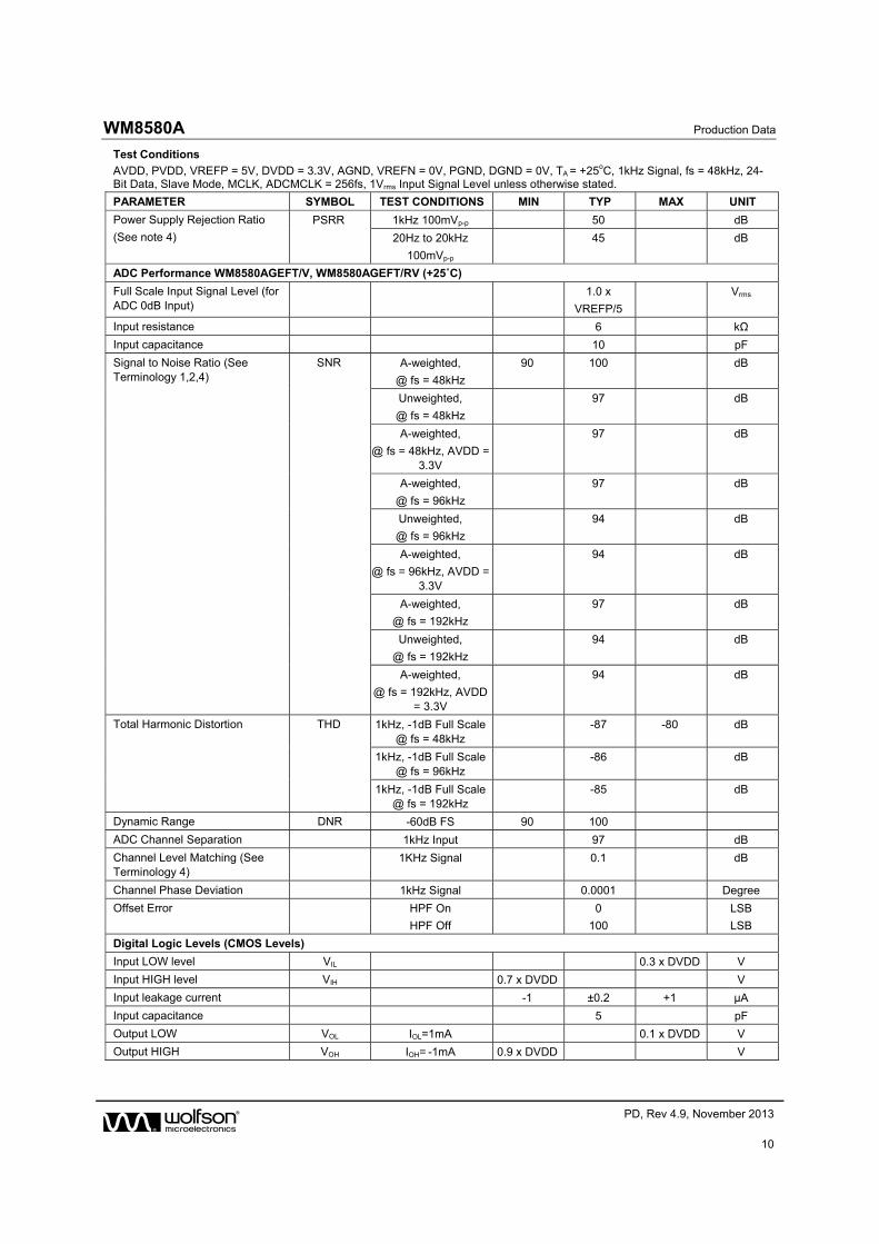
Test Conditions
AVDD, PVDD, VREFP = 5V, DVDD = 3.3V, AGND, VREFN = 0V, PGND, DGND = 0V, TA = +25oC, 1kHz Signal, fs = 48kHz, 24-Bit Data, Slave Mode, MCLK, ADCMCLK = 256fs, 1Vrms Input Signal Level unless otherwise stated.
PARAMETER SYMBOL TEST CONDITIONS MIN TYP MAX UNIT
Power Supply Rejection Ratio
(See note 4)
PSRR 1kHz 100mVp-p 50 dB
20Hz to 20kHz
100mVp-p
45 dB
ADC Performance WM8580AGEFT/V, WM8580AGEFT/RV (+25˚C)
Full Scale Input Signal Level (for ADC 0dB Input)
1.0 x
VREFP/5
Vrms
Input resistance 6 kΩ
Input capacitance 10 pF
Signal to Noise Ratio (See Terminology 1,2,4)
SNR A-weighted,
@ fs = 48kHz
90 100 dB
Unweighted,
@ fs = 48kHz
97 dB
A-weighted,
@ fs = 48kHz, AVDD = 3.3V
97 dB
A-weighted,
@ fs = 96kHz
97 dB
Unweighted,
@ fs = 96kHz
94 dB
A-weighted,
@ fs = 96kHz, AVDD = 3.3V
94 dB
A-weighted,
@ fs = 192kHz
97 dB
Unweighted,
@ fs = 192kHz
94 dB
A-weighted,
@ fs = 192kHz, AVDD = 3.3V
94 dB
Total Harmonic Distortion THD 1kHz, -1dB Full Scale @ fs = 48kHz
-87 -80 dB
1kHz, -1dB Full Scale @ fs = 96kHz
-86 dB
1kHz, -1dB Full Scale @ fs = 192kHz
-85 dB
Dynamic Range DNR -60dB FS 90 100
ADC Channel Separation 1kHz Input 97 dB
Channel Level Matching (See Terminology 4)
1KHz Signal 0.1 dB
Channel Phase Deviation 1kHz Signal 0.0001 Degree
Offset Error HPF On
HPF Off
0
100
LSB
LSB
Digital Logic Levels (CMOS Levels)
Input LOW level VIL 0.3 x DVDD V
Input HIGH level VIH 0.7 x DVDD V
Input leakage current -1 ±0.2 +1 µA
Input capacitance 5 pF
Output LOW VOL IOL=1mA 0.1 x DVDD V
Output HIGH VOH IOH= -1mA 0.9 x DVDD V
Production Data WM8580A
w PD, Rev 4.9, November 2013
11
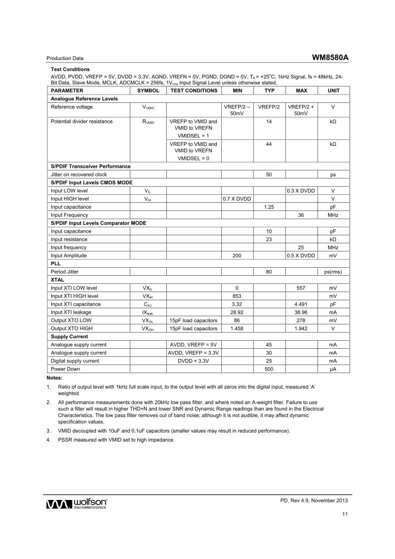
Test Conditions
AVDD, PVDD, VREFP = 5V, DVDD = 3.3V, AGND, VREFN = 0V, PGND, DGND = 0V, TA = +25oC, 1kHz Signal, fs = 48kHz, 24-Bit Data, Slave Mode, MCLK, ADCMCLK = 256fs, 1Vrms Input Signal Level unless otherwise stated.
PARAMETER SYMBOL TEST CONDITIONS MIN TYP MAX UNIT
Analogue Reference Levels
Reference voltage VVMID VREFP/2 – 50mV
VREFP/2 VREFP/2 + 50mV
V
Potential divider resistance RVMID VREFP to VMID and VMID to VREFN
VMIDSEL = 1
14 kΩ
VREFP to VMID and VMID to VREFN
VMIDSEL = 0
44 kΩ
S/PDIF Transceiver Performance
Jitter on recovered clock 50 ps
S/PDIF Input Levels CMOS MODE
Input LOW level VIL 0.3 X DVDD V
Input HIGH level VIH 0.7 X DVDD V
Input capacitance 1.25 pF
Input Frequency 36 MHz
S/PDIF Input Levels Comparator MODE
Input capacitance 10 pF
Input resistance 23 kΩ
Input frequency 25 MHz
Input Amplitude 200 0.5 X DVDD mV
PLL
Period Jitter 80 ps(rms)
XTAL
Input XTI LOW level VXIL 0 557 mV
Input XTI HIGH level VXIH 853 mV
Input XTI capacitance CXJ 3.32 4.491 pF
Input XTI leakage IXleak 28.92 38.96 mA
Output XTO LOW VXOL 15pF load capacitors 86 278 mV
Output XTO HIGH VXOH 15pF load capacitors 1.458 1.942 V
Supply Current
Analogue supply current AVDD, VREFP = 5V 45 mA
Analogue supply current AVDD, VREFP = 3.3V 30 mA
Digital supply current DVDD = 3.3V 25 mA
Power Down 500 μA
Notes:
1. Ratio of output level with 1kHz full scale input, to the output level with all zeros into the digital input, measured ‘A’ weighted.
2. All performance measurements done with 20kHz low pass filter, and where noted an A-weight filter. Failure to use such a filter will result in higher THD+N and lower SNR and Dynamic Range readings than are found in the Electrical Characteristics. The low pass filter removes out of band noise; although it is not audible, it may affect dynamic specification values.
3. VMID decoupled with 10uF and 0.1uF capacitors (smaller values may result in reduced performance).
4. PSSR measured with VMID set to high impedance
WM8580A Production Data
w PD, Rev 4.9, November 2013
12
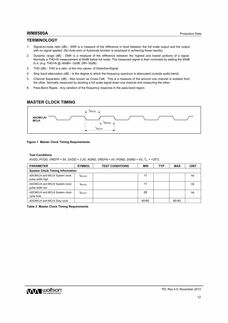
TERMINOLOGY
1. Signal-to-noise ratio (dB) - SNR is a measure of the difference in level between the full scale output and the output with no signal applied. (No Auto-zero or Automute function is employed in achieving these results).
2. Dynamic range (dB) - DNR is a measure of the difference between the highest and lowest portions of a signal. Normally a THD+N measurement at 60dB below full scale. The measured signal is then corrected by adding the 60dB to it. (e.g. THD+N @ -60dB= -32dB, DR= 92dB).
3. THD (dB) - THD is a ratio, of the rms values, of Distortion/Signal.
4. Stop band attenuation (dB) - Is the degree to which the frequency spectrum is attenuated (outside audio band).
5. Channel Separation (dB) - Also known as Cross-Talk. This is a measure of the amount one channel is isolated from the other. Normally measured by sending a full scale signal down one channel and measuring the other.
6. Pass-Band Ripple - Any variation of the frequency response in the pass-band region.
MASTER CLOCK TIMING
ADCMCLK/MCLK
t MCLKL
tMCLKH
tMCLKY
Figure 1 Master Clock Timing Requirements
Test Conditions
AVDD, PVDD, VREFP = 5V, DVDD = 3.3V, AGND, VREFN = 0V, PGND, DGND = 0V, TA = +25oC
PARAMETER SYMBOL TEST CONDITIONS MIN TYP MAX UNIT
System Clock Timing Information
ADCMCLK and MCLK System clock
pulse width high
tMCLKH 11 ns
ADCMCLK and MCLK System clock
pulse width low
tMCLKL 11 ns
ADCMCLK and MCLK System clock
cycle time
tMCLKY 28 ns
ADCMCLK and MCLK Duty cycle 40:60 60:40
Table 3 Master Clock Timing Requirements
Production Data WM8580A
w PD, Rev 4.9, November 2013
13
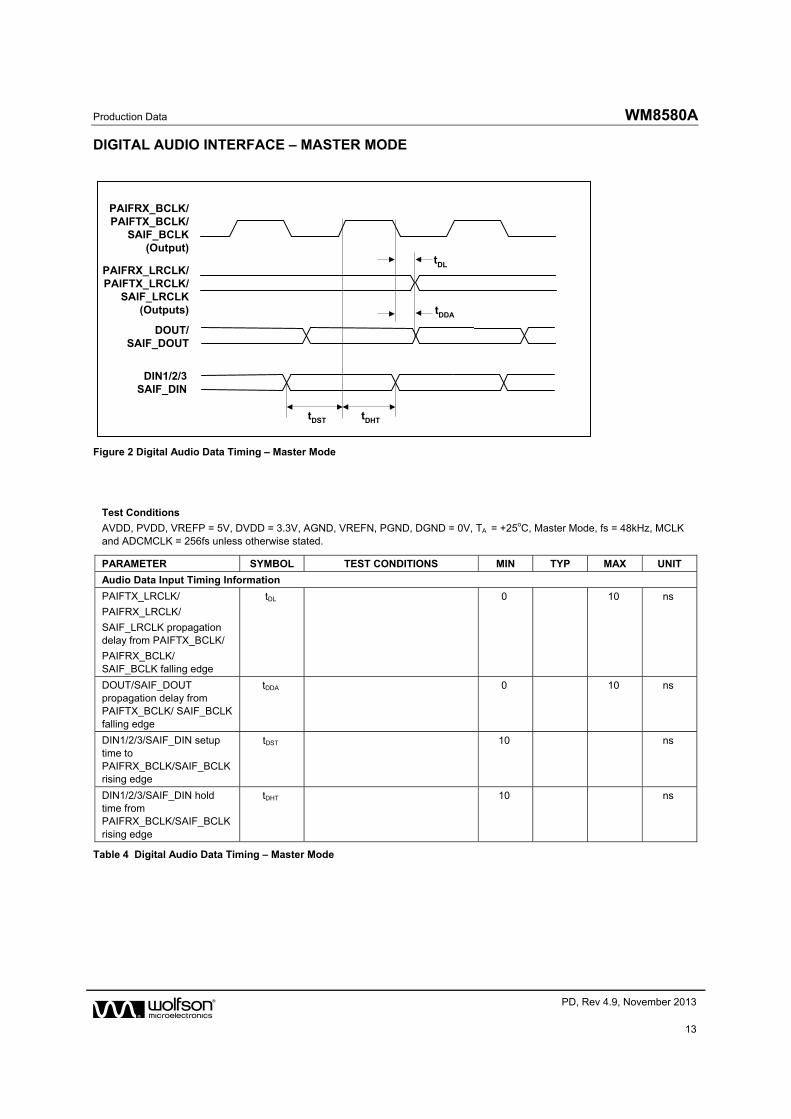
DIGITAL AUDIO INTERFACE – MASTER MODE
PAIFRX_BCLK/PAIFTX_BCLK/
SAIF_BCLK(Output)
DOUT/SAIF_DOUT
PAIFRX_LRCLK/PAIFTX_LRCLK/
SAIF_LRCLK(Outputs)
tDL
DIN1/2/3SAIF_DIN
tDDA
tDHTtDST
Figure 2 Digital Audio Data Timing – Master Mode
Test Conditions
AVDD, PVDD, VREFP = 5V, DVDD = 3.3V, AGND, VREFN, PGND, DGND = 0V, TA = +25oC, Master Mode, fs = 48kHz, MCLK and ADCMCLK = 256fs unless otherwise stated.
PARAMETER SYMBOL TEST CONDITIONS MIN TYP MAX UNIT
Audio Data Input Timing Information
PAIFTX_LRCLK/
PAIFRX_LRCLK/
SAIF_LRCLK propagation delay from PAIFTX_BCLK/
PAIFRX_BCLK/ SAIF_BCLK falling edge
tDL 0 10 ns
DOUT/SAIF_DOUT propagation delay from PAIFTX_BCLK/ SAIF_BCLK falling edge
tDDA 0 10 ns
DIN1/2/3/SAIF_DIN setup time to PAIFRX_BCLK/SAIF_BCLK rising edge
tDST 10 ns
DIN1/2/3/SAIF_DIN hold time from PAIFRX_BCLK/SAIF_BCLK rising edge
tDHT 10 ns
Table 4 Digital Audio Data Timing – Master Mode
WM8580A Production Data
w PD, Rev 4.9, November 2013
14
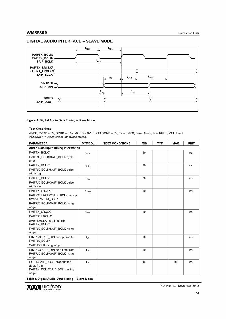
DIGITAL AUDIO INTERFACE – SLAVE MODE
PAIFTX_BCLK/PAIFRX_BCLK/
SAIF_BCLK
PAIFTX_LRCLK/PAIFRX_LRCLK/
SAIF_BCLK
DIN1/2/3/SAIF_DIN
DOUT/SAIF_DOUT
tBCH tBCL
tBCY
tLRSUtDS tLRH
tDHtDD
Figure 3 Digital Audio Data Timing – Slave Mode
Test Conditions
AVDD, PVDD = 5V, DVDD = 3.3V, AGND = 0V, PGND,DGND = 0V, TA = +25oC, Slave Mode, fs = 48kHz, MCLK and ADCMCLK = 256fs unless otherwise stated.
PARAMETER SYMBOL TEST CONDITIONS MIN TYP MAX UNIT
Audio Data Input Timing Information
PAIFTX_BCLK/
PAIFRX_BCLK/SAIF_BCLK cycle time
tBCY 50 ns
PAIFTX_BCLK/
PAIFRX_BCLK/SAIF_BCLK pulse width high
tBCH 20 ns
PAIFTX_BCLK/
PAIFRX_BCLK/SAIF_BCLK pulse width low
tBCL 20 ns
PAIFTX_LRCLK/
PAIFRX_LRCLK/SAIF_BCLK set-up time to PAIFTX_BCLK/
PAIFRX_BCLK/SAIF_BCLK rising edge
tLRSU 10 ns
PAIFTX_LRCLK/
PAIFRX_LRCLK/
SAIF_LRCLK hold time from PAIFTX_BCLK/
PAIFRX_BCLK/SAIF_BCLK rising edge
tLRH 10 ns
DIN1/2/3/SAIF_DIN set-up time to PAIFRX_BCLK/
SAIF_BCLK rising edge
tDS 10 ns
DIN1/2/3/SAIF_DIN hold time from PAIFRX_BCLK/SAIF_BCLK rising edge
tDH 10 ns
DOUT/SAIF_DOUT propagation delay from PAIFTX_BCLK/SAIF_BCLK falling edge
tDD 0 10 ns
Table 5 Digital Audio Data Timing – Slave Mode
Production Data WM8580A
w PD, Rev 4.9, November 2013
15
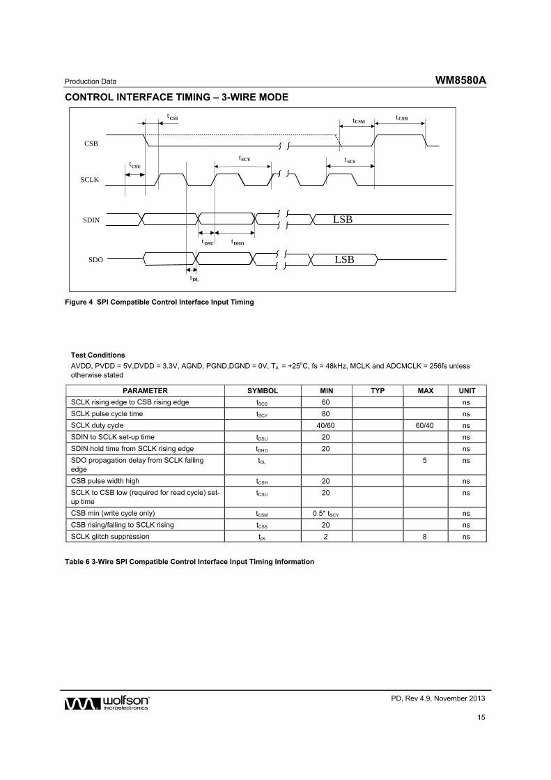
CONTROL INTERFACE TIMING – 3-WIRE MODE
CSB
SCLK
SDIN
tDHOt DSU
tCSH
tSCY t SCS
LSB
SDO
tDL
LSB
tCSS
tCSU
tCSM
Figure 4 SPI Compatible Control Interface Input Timing
Test Conditions
AVDD, PVDD = 5V,DVDD = 3.3V, AGND, PGND,DGND = 0V, TA = +25oC, fs = 48kHz, MCLK and ADCMCLK = 256fs unless otherwise stated
PARAMETER SYMBOL MIN TYP MAX UNIT
SCLK rising edge to CSB rising edge tSCS 60 ns
SCLK pulse cycle time tSCY 80 ns
SCLK duty cycle 40/60 60/40 ns
SDIN to SCLK set-up time tDSU 20 ns
SDIN hold time from SCLK rising edge tDHO 20 ns
SDO propagation delay from SCLK falling edge
tDL 5 ns
CSB pulse width high tCSH 20 ns
SCLK to CSB low (required for read cycle) set-up time
tCSU 20 ns
CSB min (write cycle only) tCSM 0.5* tSCY ns
CSB rising/falling to SCLK rising tCSS 20 ns
SCLK glitch suppression tps 2 8 ns
Table 6 3-Wire SPI Compatible Control Interface Input Timing Information
WM8580A Production Data
w PD, Rev 4.9, November 2013
16
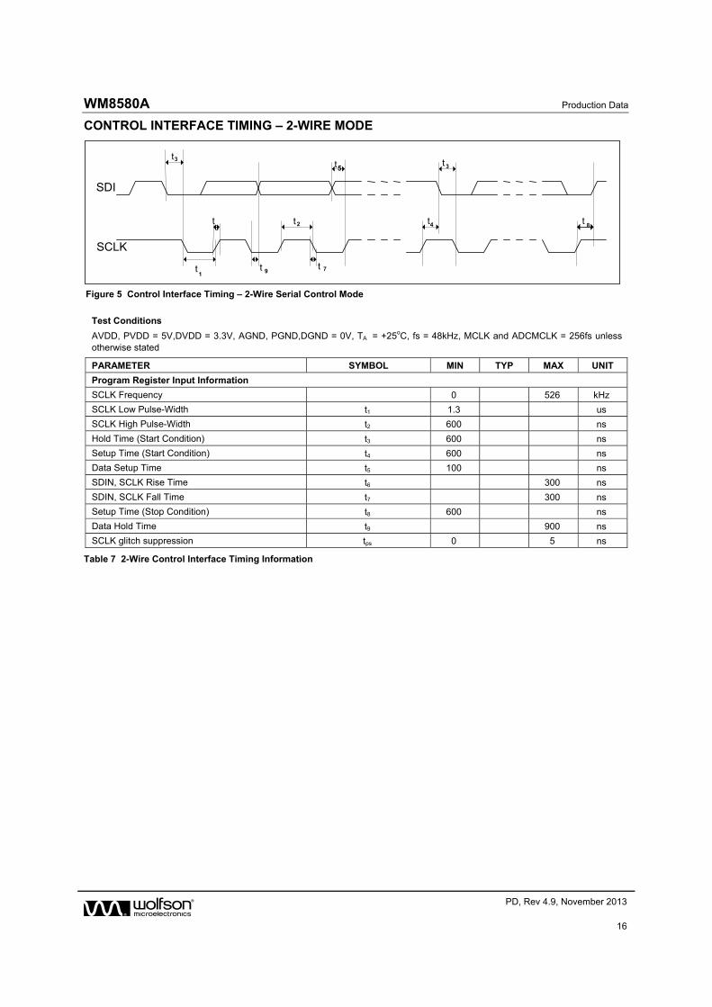
CONTROL INTERFACE TIMING – 2-WIRE MODE
Figure 5 Control Interface Timing – 2-Wire Serial Control Mode
Test Conditions
AVDD, PVDD = 5V,DVDD = 3.3V, AGND, PGND,DGND = 0V, TA = +25oC, fs = 48kHz, MCLK and ADCMCLK = 256fs unless otherwise stated
PARAMETER SYMBOL MIN TYP MAX UNIT
Program Register Input Information
SCLK Frequency 0 526 kHz
SCLK Low Pulse-Width t1 1.3 us
SCLK High Pulse-Width t2 600 ns
Hold Time (Start Condition) t3 600 ns
Setup Time (Start Condition) t4 600 ns
Data Setup Time t5 100 ns
SDIN, SCLK Rise Time t6 300 ns
SDIN, SCLK Fall Time t7 300 ns
Setup Time (Stop Condition) t8 600 ns
Data Hold Time t9 900 ns
SCLK glitch suppression tps 0 5 ns
Table 7 2-Wire Control Interface Timing Information
t3
t1
t6
t 9
t2
t5
t 7
t 3
t4 t 8
SDI
SCLK
Production Data WM8580A
w PD, Rev 4.9, November 2013
17
DEVICE DESCRIPTION
INTRODUCTION
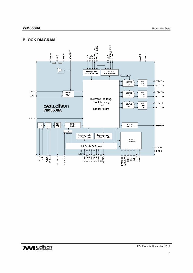
WM8580A is a complete mutli-channel CODEC with integrated S/PDIF transceiver. The device comprises three separate stereo DACs and a stereo ADC, in a single package, and controlled by either software or hardware interfaces.
The three stereo DAC outputs are ideal to implement a complete 5.1 channel surround system. Each DAC has its own digital volume control (adjustable in 0.5dB steps) with zero cross detection. With zero cross enabled, volume updates occur as a signal transitions through its zero point. This minimises audible clicks and ‘zipper’ noise as the gain values change.
Each stereo DAC has its own data input (DIN1/2/3) and shared word clock (PAIFRX_LRCLK), bit clock (PAIFRX_BCLK) and master clock (MCLK). The stereo ADC has data output (DOUT), word clock (PAIFTX_LRCLK), and bit clock (PAIFTX_BCLK). This allows the ADC to operate at a different sample rate to the DACs. In addition, a separate ADC master clock (ADCMCLK) can be used instead of MCLK for further flexibility.
There are two independent Digital Audio Interfaces, which may be configured to operate in either master or slave mode. In Slave mode, the LRCLKs and BCLKs are inputs. In Master mode, the LRCLKs and BCLKs are outputs.
The Audio Interfaces support Right Justified, Left Justified, I2S and DSP formats. Word lengths of 16, 20, 24 and 32 bits are available (with the exception of 32 bit Right Justified).
Operation using system clocks of 128fs, 192fs, 256fs, 384fs, 512fs, 768fs or 1152fs is provided. In Slave mode, selection between clock rates is automatically controlled. In master mode, the master clock to sample rate ratio is set by register control. Sample rates (fs) from less than 8ks/s up to 192ks/s are permitted providing the appropriate system clock is input.
The S/PDIF Transceiver is IEC-60958-3 compatible with 32k frames/s to 96k frames/s support. S/PDIF data can be input on one of four pins, and routed internally to the Audio Interfaces, DAC1, and S/PDIF transmitter. Error flags and status information can be read back over the serial interface, or output on GPO pins. The S/PDIF Transmitter can source data from the ADC, S/PDIF Receiver or Audio Interfaces. The Transceiver supports Consumer Mode Channel information, and transmitted Channel bits can be configured via register control.
The Digital Routing paths between all the interfaces can be configured by the user, as can the corresponding interface clocking schemes.
There are two PLLs, which can be independently configured to generate two system clocks for internal or external use.
The serial control interface is controlled by pins CSB, SCLK, and SDIN, which are 5V tolerant with TTL input thresholds, allowing the WM8580A to be used with DVDD = 3.3V and be controlled by a controller with 5V output. SDO allows status registers to be read back over the serial interface (SDO is not 5V tolerant).
The WM8580A may also be controlled in hardware mode, selected by the HWMODE pin. In hardware mode, limited control of internal functionality is available via the Multi-Function Pins (MFPs) and CSB, SCLK, SDIN and MUTE pins.
WM8580A Production Data
w PD, Rev 4.9, November 2013
18
CONTROL INTERFACE OPERATION
Control of the WM8580A is implemented either in Hardware Control Mode or Software Control Mode. The method of control is determined by the state of the HWMODE pin. If the HWMODE pin is low, Software Control Mode is selected. If the HWMODE pin is high, Hardware Control Mode is selected. The Software Control Interface is described below and Hardware Control Mode is described on page 70
Software control is implemented with a 3-wire (3-wire write, 4-wire read, SPI compatible) or 2-wire read/write serial interface.
The interface configuration is determined by the state of the SWMODE pin. If the SWMODE pin is low, the 2-wire configuration is selected. If SWMODE is high the 3-wire SPI compatible configuration is selected.
HWMODE SWMODE
0 1 0 1
Software Control Hardware Control 2-wire control 3-wire control
Table 8 Hardware/Software Mode Setup
The control interface is 5V tolerant, meaning that the control interface input signals CSB, SCLK and SDIN may have an input high level of 5V while DVDD is 3V. Input thresholds are determined by DVDD.
3-WIRE (SPI COMPATIBLE) SERIAL CONTROL MODE WITH READ-BACK
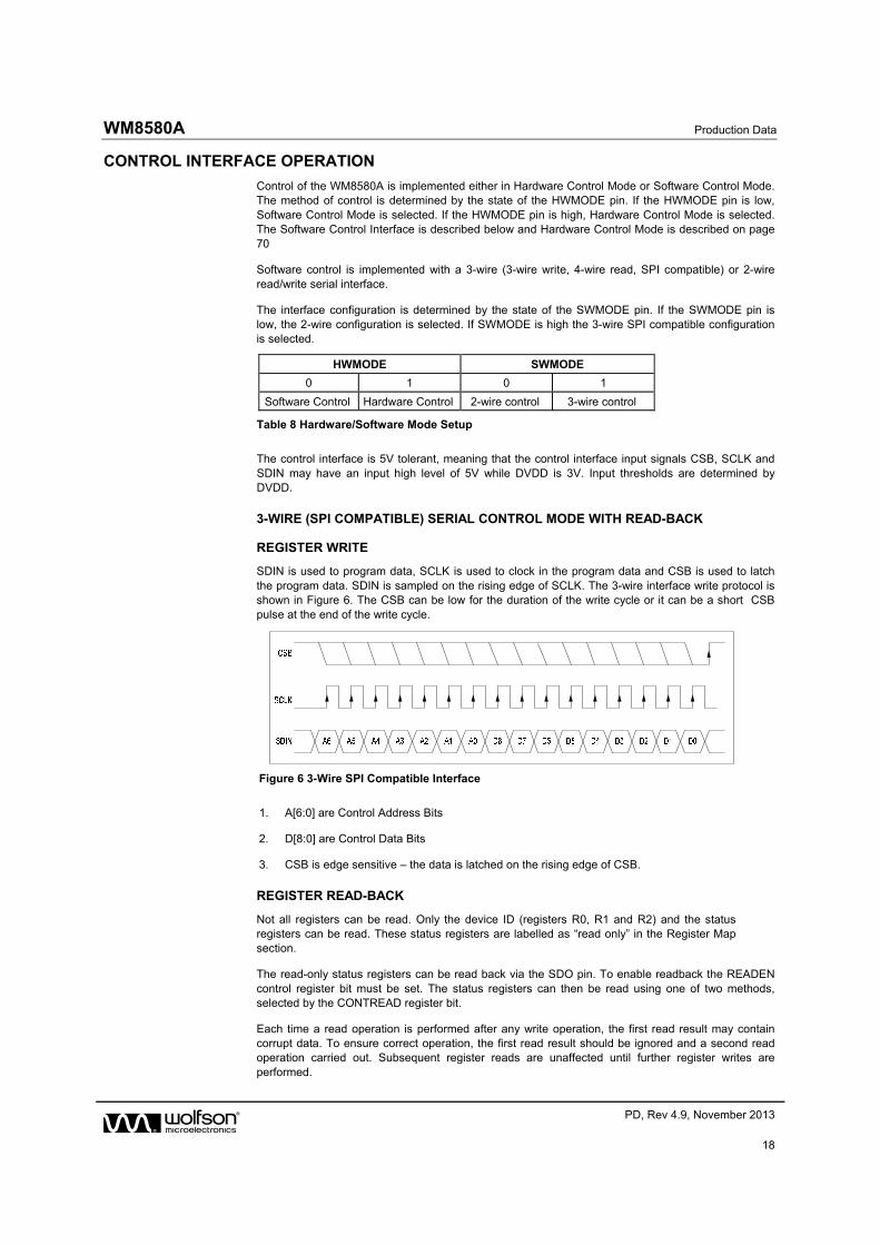
REGISTER WRITE
SDIN is used to program data, SCLK is used to clock in the program data and CSB is used to latch the program data. SDIN is sampled on the rising edge of SCLK. The 3-wire interface write protocol is shown in Figure 6. The CSB can be low for the duration of the write cycle or it can be a short CSB pulse at the end of the write cycle.
Figure 6 3-Wire SPI Compatible Interface
1. A[6:0] are Control Address Bits
2. D[8:0] are Control Data Bits
3. CSB is edge sensitive – the data is latched on the rising edge of CSB.
REGISTER READ-BACK
Not all registers can be read. Only the device ID (registers R0, R1 and R2) and the status registers can be read. These status registers are labelled as “read only” in the Register Map section.
The read-only status registers can be read back via the SDO pin. To enable readback the READEN control register bit must be set. The status registers can then be read using one of two methods, selected by the CONTREAD register bit.
Each time a read operation is performed after any write operation, the first read result may contain corrupt data. To ensure correct operation, the first read result should be ignored and a second read operation carried out. Subsequent register reads are unaffected until further register writes are performed.
Production Data WM8580A
w PD, Rev 4.9, November 2013
19
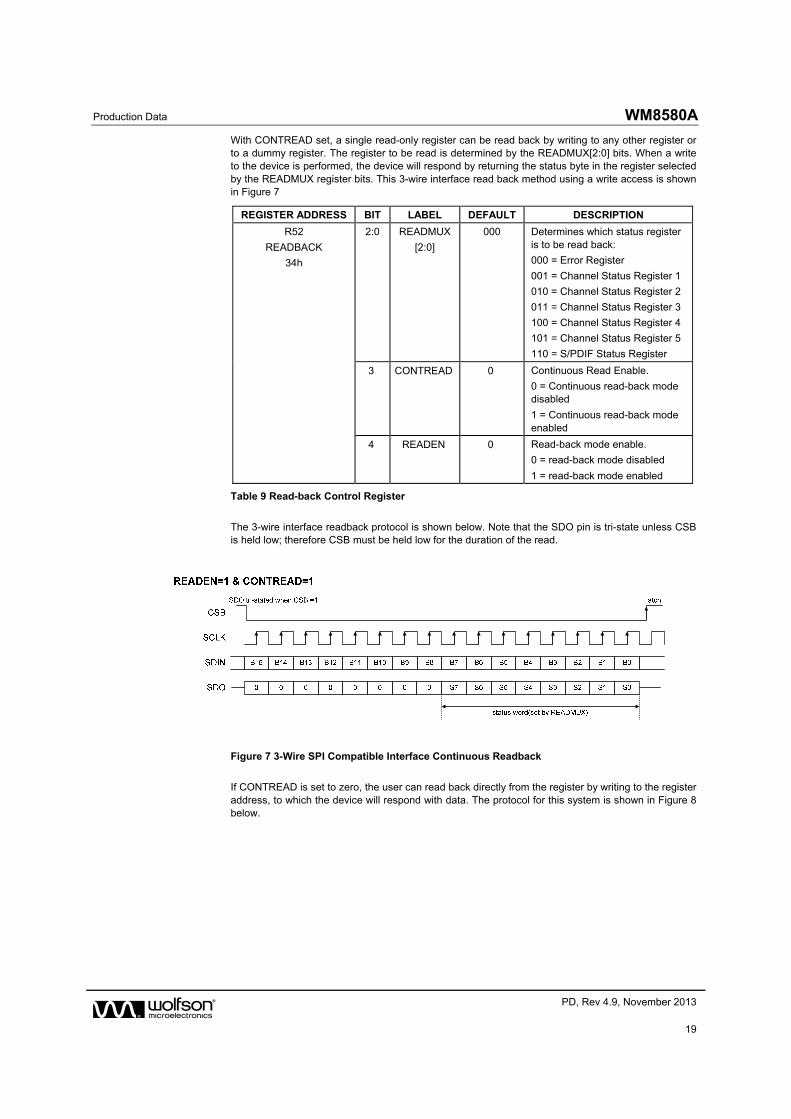
With CONTREAD set, a single read-only register can be read back by writing to any other register or to a dummy register. The register to be read is determined by the READMUX[2:0] bits. When a write to the device is performed, the device will respond by returning the status byte in the register selected by the READMUX register bits. This 3-wire interface read back method using a write access is shown in Figure 7
REGISTER ADDRESS BIT LABEL DEFAULT DESCRIPTION
R52
READBACK
34h
2:0 READMUX
[2:0]
000 Determines which status register is to be read back:
000 = Error Register
001 = Channel Status Register 1
010 = Channel Status Register 2
011 = Channel Status Register 3
100 = Channel Status Register 4
101 = Channel Status Register 5
110 = S/PDIF Status Register
3 CONTREAD 0 Continuous Read Enable.
0 = Continuous read-back mode disabled
1 = Continuous read-back mode enabled
4 READEN 0 Read-back mode enable.
0 = read-back mode disabled
1 = read-back mode enabled
Table 9 Read-back Control Register
The 3-wire interface readback protocol is shown below. Note that the SDO pin is tri-state unless CSB is held low; therefore CSB must be held low for the duration of the read.
Figure 7 3-Wire SPI Compatible Interface Continuous Readback
If CONTREAD is set to zero, the user can read back directly from the register by writing to the register address, to which the device will respond with data. The protocol for this system is shown in Figure 8 below.
WM8580A Production Data
w PD, Rev 4.9, November 2013
20
Figure 8 3-Wire SPI Compatible Control Interface Non-Continuous Readback
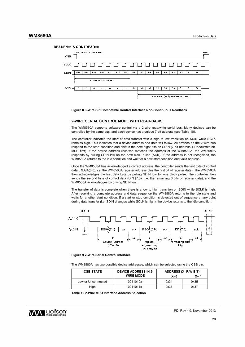
2-WIRE SERIAL CONTROL MODE WITH READ-BACK
The WM8580A supports software control via a 2-wire read/write serial bus. Many devices can be controlled by the same bus, and each device has a unique 7-bit address (see Table 10).
The controller indicates the start of data transfer with a high to low transition on SDIN while SCLK remains high. This indicates that a device address and data will follow. All devices on the 2-wire bus respond to the start condition and shift in the next eight bits on SDIN (7-bit address + Read/Write bit, MSB first). If the device address received matches the address of the WM8580A, the WM8580A responds by pulling SDIN low on the next clock pulse (ACK). If the address is not recognised, the WM8580A returns to the idle condition and wait for a new start condition and valid address.
Once the WM8580A has acknowledged a correct address, the controller sends the first byte of control data (REGA(6:0), i.e. the WM8580A register address plus the first bit of register data). The WM8580A then acknowledges the first data byte by pulling SDIN low for one clock pulse. The controller then sends the second byte of control data (DIN (7:0),, i.e. the remaining 8 bits of register data), and the WM8580A acknowledges by driving SDIN low.
The transfer of data is complete when there is a low to high transition on SDIN while SCLK is high. After receiving a complete address and data sequence the WM8580A returns to the idle state and waits for another start condition. If a start or stop condition is detected out of sequence at any point during data transfer (i.e. SDIN changes while SCLK is high), the device returns to the idle condition.
Figure 9 2-Wire Serial Control Interface
The WM8580A has two possible device addresses, which can be selected using the CSB pin.
CSB STATE DEVICE ADDRESS IN 2-WIRE MODE
ADDRESS (X=R/W BIT)
X=0 X= 1
Low or Unconnected 0011010x 0x34 0x35
High 0011011x 0x36 0x37
Table 10 2-Wire MPU Interface Address Selection
Production Data WM8580A
w PD, Rev 4.9, November 2013
21
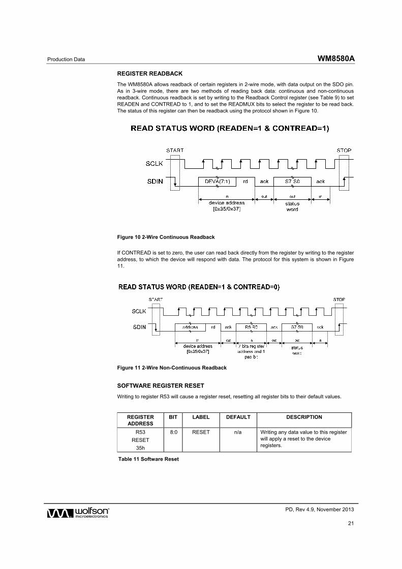
REGISTER READBACK
The WM8580A allows readback of certain registers in 2-wire mode, with data output on the SDO pin. As in 3-wire mode, there are two methods of reading back data: continuous and non-continuous readback. Continuous readback is set by writing to the Readback Control register (see Table 9) to set READEN and CONTREAD to 1, and to set the READMUX bits to select the register to be read back. The status of this register can then be readback using the protocol shown in Figure 10.
Figure 10 2-Wire Continuous Readback
If CONTREAD is set to zero, the user can read back directly from the register by writing to the register address, to which the device will respond with data. The protocol for this system is shown in Figure 11.
Figure 11 2-Wire Non-Continuous Readback
SOFTWARE REGISTER RESET
Writing to register R53 will cause a register reset, resetting all register bits to their default values.
Table 11 Software Reset
REGISTER ADDRESS
BIT LABEL DEFAULT DESCRIPTION
R53
RESET
35h
8:0 RESET n/a Writing any data value to this register will apply a reset to the device registers.
WM8580A Production Data
w PD, Rev 4.9, November 2013
22
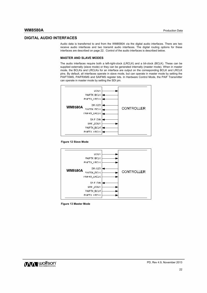
DIGITAL AUDIO INTERFACES
Audio data is transferred to and from the WM8580A via the digital audio interfaces. There are two receive audio interfaces and two transmit audio interfaces. The digital routing options for these interfaces are described on page 22. Control of the audio interfaces is described below.
MASTER AND SLAVE MODES
The audio interfaces require both a left-right-clock (LRCLK) and a bit-clock (BCLK). These can be supplied externally (slave mode) or they can be generated internally (master mode). When in master mode, the BCLKs and LRCLKs for an interface are output on the corresponding BCLK and LRCLK pins. By default, all interfaces operate in slave mode, but can operate in master mode by setting the PAIFTXMS, PAIFRXMS and SAIFMS register bits. In Hardware Control Mode, the PAIF Transmitter can operate in master mode by setting the SDI pin.
Figure 12 Slave Mode
Figure 13 Master Mode
Production Data WM8580A
w PD, Rev 4.9, November 2013
23
REGISTER ADDRESS
BIT LABEL DEFAULT DESCRIPTION
R9
PAIF 1
09h
5 PAIFRXMS
0 PAIF Receiver Master/Slave Mode Select:
0 = Slave Mode
1 = Master Mode
R10
PAIF 2
0Ah
5 PAIFTXMS
0 PAIF Transmitter Master/Slave Mode Select:
0 = Slave Mode
1 = Master Mode
R11
SAIF 1
0Bh
5 SAIFMS 0 SAIF Master/Slave Mode Select:
0 = Slave Mode
1 = Master Mode
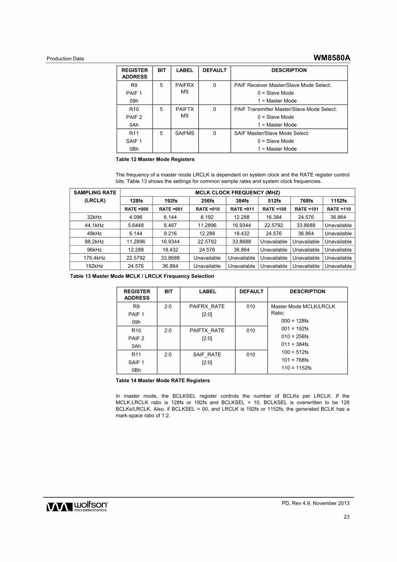
Table 12 Master Mode Registers
The frequency of a master mode LRCLK is dependant on system clock and the RATE register control bits. Table 13 shows the settings for common sample rates and system clock frequencies.
SAMPLING RATE
(LRCLK)
MCLK CLOCK FREQUENCY (MHZ)
128fs 192fs 256fs 384fs 512fs 768fs 1152fs
RATE =000 RATE =001 RATE =010 RATE =011 RATE =100 RATE =101 RATE =110
32kHz 4.096 6.144 8.192 12.288 16.384 24.576 36.864
44.1kHz 5.6448 8.467 11.2896 16.9344 22.5792 33.8688 Unavailable
48kHz 6.144 9.216 12.288 18.432 24.576 36.864 Unavailable
88.2kHz 11.2896 16.9344 22.5792 33.8688 Unavailable Unavailable Unavailable
96kHz 12.288 18.432 24.576 36.864 Unavailable Unavailable Unavailable
176.4kHz 22.5792 33.8688 Unavailable Unavailable Unavailable Unavailable Unavailable
192kHz 24.576 36.864 Unavailable Unavailable Unavailable Unavailable Unavailable
Table 13 Master Mode MCLK / LRCLK Frequency Selection
REGISTER ADDRESS
BIT LABEL DEFAULT DESCRIPTION
R9
PAIF 1
09h
2:0 PAIFRX_RATE
[2:0]
010 Master Mode MCLK/LRCLK Ratio:
000 = 128fs
001 = 192fs
010 = 256fs
011 = 384fs
100 = 512fs
101 = 768fs
110 = 1152fs
R10
PAIF 2
0Ah
2:0 PAIFTX_RATE
[2:0]
010
R11
SAIF 1
0Bh
2:0 SAIF_RATE
[2:0]
010
Table 14 Master Mode RATE Registers
In master mode, the BCLKSEL register controls the number of BCLKs per LRCLK. If the MCLK:LRCLK ratio is 128fs or 192fs and BCLKSEL = 10, BCLKSEL is overwritten to be 128 BCLKs/LRCLK. Also, if BCLKSEL = 00, and LRCLK is 192fs or 1152fs, the generated BCLK has a mark-space ratio of 1:2.
WM8580A Production Data
w PD, Rev 4.9, November 2013
24
REGISTER ADDRESS
BIT LABEL DEFAULT DESCRIPTION
R9
PAIF 1
09h
4:3 PAIFRX_BCLKSEL
[1:0]
00 Master Mode BCLK Rate:
00 = 64 BCLKs per LRCLK
01 = 32 BCLKs per LRCLK
10 = 16 BCLKs per LRCLK
11 = BCLK = System Clock.
R10
PAIF 2
0Ah
4:3 PAIFTX_BCLKSEL
[1:0]
00
R11
SAIF 1
0Bh
4:3 SAIF_BCLKSEL
[1:0]
00
Table 15 Master Mode BCLK Control
AUDIO DATA FORMATS
Five popular interface formats are supported:
Left Justified mode
Right Justified mode
I2S mode
DSP Mode A
DSP Mode B
All five formats send the MSB first and support word lengths of 16, 20, 24 and 32 bits, with the exception of 32 bit right justified mode, which is not supported.
Audio Data for each stereo channel is time multiplexed with the interface’s Left-Right-Clock (LRCLK), indicating whether the left or right channel is present. The LRCLK is also used as a timing reference to indicate the beginning or end of the data words.
In Left Justified, Right Justified and I2S modes, the minimum number of BCLKs per LRCLK period is 2 times the selected word length. LRCLK must be high for a minimum of BCLK periods equivalent to the audio word length, and low for minimum of the same number of BCLK periods. Any mark to space ratio on LRCLK is acceptable provided these requirements are met.
Production Data WM8580A
w PD, Rev 4.9, November 2013
25
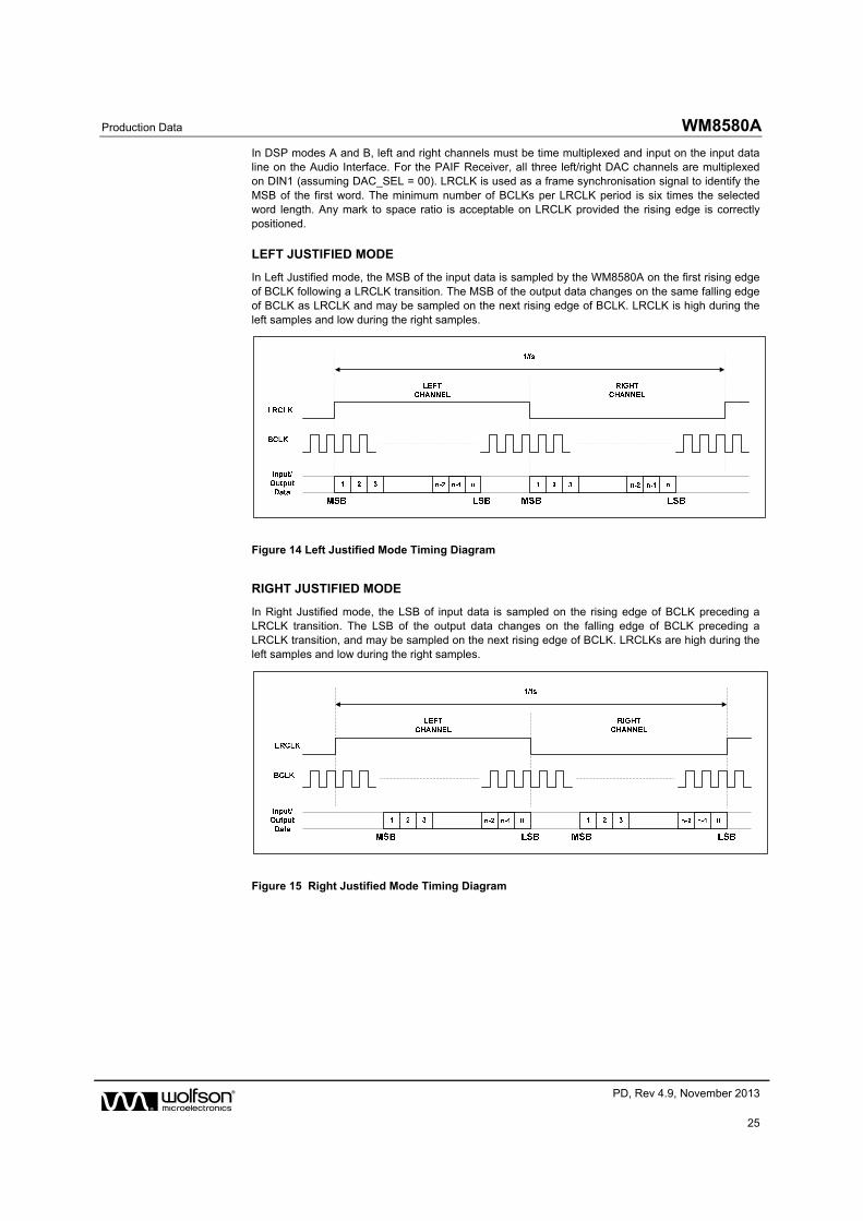
In DSP modes A and B, left and right channels must be time multiplexed and input on the input data line on the Audio Interface. For the PAIF Receiver, all three left/right DAC channels are multiplexed on DIN1 (assuming DAC_SEL = 00). LRCLK is used as a frame synchronisation signal to identify the MSB of the first word. The minimum number of BCLKs per LRCLK period is six times the selected word length. Any mark to space ratio is acceptable on LRCLK provided the rising edge is correctly positioned.
LEFT JUSTIFIED MODE
In Left Justified mode, the MSB of the input data is sampled by the WM8580A on the first rising edge of BCLK following a LRCLK transition. The MSB of the output data changes on the same falling edge of BCLK as LRCLK and may be sampled on the next rising edge of BCLK. LRCLK is high during the left samples and low during the right samples.
Figure 14 Left Justified Mode Timing Diagram
RIGHT JUSTIFIED MODE
In Right Justified mode, the LSB of input data is sampled on the rising edge of BCLK preceding a LRCLK transition. The LSB of the output data changes on the falling edge of BCLK preceding a LRCLK transition, and may be sampled on the next rising edge of BCLK. LRCLKs are high during the left samples and low during the right samples.
Figure 15 Right Justified Mode Timing Diagram
WM8580A Production Data
w PD, Rev 4.9, November 2013
26
I2S MODE
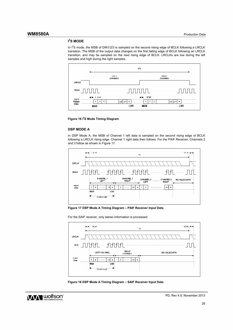
In I2S mode, the MSB of DIN1/2/3 is sampled on the second rising edge of BCLK following a LRCLK transition. The MSB of the output data changes on the first falling edge of BCLK following an LRCLK transition, and may be sampled on the next rising edge of BCLK. LRCLKs are low during the left samples and high during the right samples.
Figure 16 I2S Mode Timing Diagram
DSP MODE A
In DSP Mode A, the MSB of Channel 1 left data is sampled on the second rising edge of BCLK following a LRCLK rising edge. Channel 1 right data then follows. For the PAIF Receiver, Channels 2 and 3 follow as shown in Figure 17.
Figure 17 DSP Mode A Timing Diagram – PAIF Receiver Input Data
For the SAIF receiver, only stereo information is processed.
Figure 18 DSP Mode A Timing Diagram – SAIF Receiver Input Data
Production Data WM8580A
w PD, Rev 4.9, November 2013
27
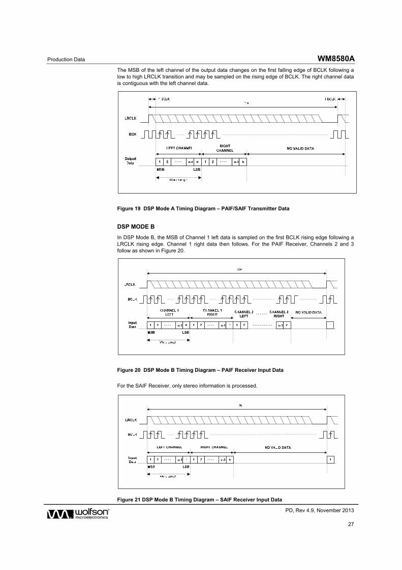
The MSB of the left channel of the output data changes on the first falling edge of BCLK following a low to high LRCLK transition and may be sampled on the rising edge of BCLK. The right channel data is contiguous with the left channel data.
Figure 19 DSP Mode A Timing Diagram – PAIF/SAIF Transmitter Data
DSP MODE B
In DSP Mode B, the MSB of Channel 1 left data is sampled on the first BCLK rising edge following a LRCLK rising edge. Channel 1 right data then follows. For the PAIF Receiver, Channels 2 and 3 follow as shown in Figure 20.
Figure 20 DSP Mode B Timing Diagram – PAIF Receiver Input Data
For the SAIF Receiver, only stereo information is processed.
Figure 21 DSP Mode B Timing Diagram – SAIF Receiver Input Data
WM8580A Production Data
w PD, Rev 4.9, November 2013
28
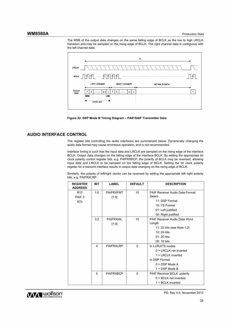
The MSB of the output data changes on the same falling edge of BCLK as the low to high LRCLK transition and may be sampled on the rising edge of BCLK. The right channel data is contiguous with the left channel data.
Figure 22 DSP Mode B Timing Diagram – PAIF/SAIF Transmitter Data
AUDIO INTERFACE CONTROL
The register bits controlling the audio interfaces are summarized below. Dynamically changing the audio data format may cause erroneous operation, and is not recommended.
Interface timing is such that the input data and LRCLK are sampled on the rising edge of the interface BCLK. Output data changes on the falling edge of the interface BCLK. By setting the appropriate bit clock polarity control register bits, e.g. PAIFRXBCP, the polarity of BCLK may be reversed, allowing input data and LRCLK to be sampled on the falling edge of BCLK. Setting the bit clock polarity register for a transmit interface results in output data changing on the rising edge of BCLK.
Similarly, the polarity of left/right clocks can be reversed by setting the appropriate left right polarity bits, e.g. PAIFRXLRP.
REGISTER ADDRESS
BIT LABEL DEFAULT DESCRIPTION
R12
PAIF 3
0Ch
1:0 PAIFRXFMT
[1:0]
10 PAIF Receiver Audio Data Format Select
11: DSP Format
10: I2S Format
01: Left justified
00: Right justified
3:2 PAIFRXWL
[1:0]
10 PAIF Receiver Audio Data Word Length
11: 32 bits (see Note 1,2)
10: 24 bits
01: 20 bits
00: 16 bits
4 PAIFRXLRP 0 In LJ/RJ/I2S modes
0 = LRCLK not inverted
1 = LRCLK inverted
In DSP Format:
0 = DSP Mode A
1 = DSP Mode B
5 PAIFRXBCP 0 PAIF Receiver BCLK polarity
0 = BCLK not inverted
1 = BCLK inverted
Production Data WM8580A
w PD, Rev 4.9, November 2013
29
REGISTER ADDRESS
BIT LABEL DEFAULT DESCRIPTION
R13
PAIF 4
0Dh
1:0 PAIFTXFMT
[1:0]
10 PAIF Transmitter Audio Data Format Select
11: DSP Format
10: I2S Format
01: Left justified
00: Right justified
3:2 PAIFTXWL
[1:0]
10 PAIF Transmitter Audio Data Word Length
11: 32 bits (see Note 1,2)
10: 24 bits
01: 20 bits
00: 16 bits
4 PAIFTXLRP 0 In LJ/RJ/I2S modes
0 = LRCLK not inverted
1 = LRCLK inverted
In DSP Format:
0 = DSP Mode A
1 = DSP Mode B
5 PAIFTXBCP 0 PAIF Receiver BCLK polarity
0 = BCLK not inverted
1 = BCLK inverted
R14
SAIF 2
0Eh
1:0 SAIFFMT
[1:0]
10 SAIF Audio Data Format Select
11: DSP Format
10: I2S Format
01: Left justified
00: Right justified
3:2 SAIFWL
[1:0]
10 SAIF Audio Data Word Length
11: 32 bits (see Note 1,2)
10: 24 bits
01: 20 bits
00: 16 bits
4 SAIFLRP 0 In LJ/RJ/I2S modes
0 = LRCLK not inverted
1 = LRCLK inverted
In DSP Format:
0 = DSP Mode A
1 = DSP Mode B
5 SAIFBCP 0 SAIF BCLK polarity
0 = BCLK not inverted
1 = BCLK inverted
6 SAIF_EN 0 SAIF Enable
0 = SAIF disabled
1 = SAIF enabled
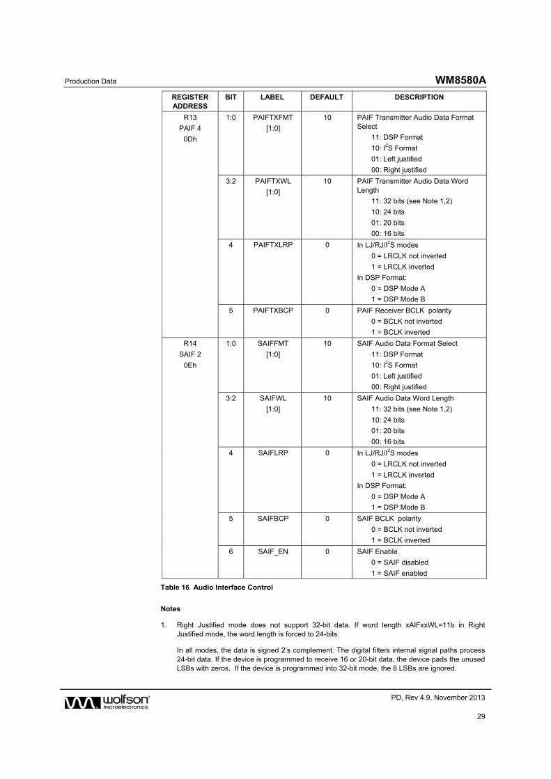
Table 16 Audio Interface Control
Notes
1. Right Justified mode does not support 32-bit data. If word length xAIFxxWL=11b in Right Justified mode, the word length is forced to 24-bits.
In all modes, the data is signed 2’s complement. The digital filters internal signal paths process 24-bit data. If the device is programmed to receive 16 or 20-bit data, the device pads the unused LSBs with zeros. If the device is programmed into 32-bit mode, the 8 LSBs are ignored.
WM8580A Production Data
w PD, Rev 4.9, November 2013
30
2. In 24-bit I2S mode, any data width of 24 bits or less is supported provided that LRCLK is high for a minimum of 24 BCLK cycles and low for a minimum of 24 BCLK cycles. If exactly 32-bit clocks occur in one full left/right clock period the interface will auto detect and configure a 16-bit data word length.
DAC FEATURES
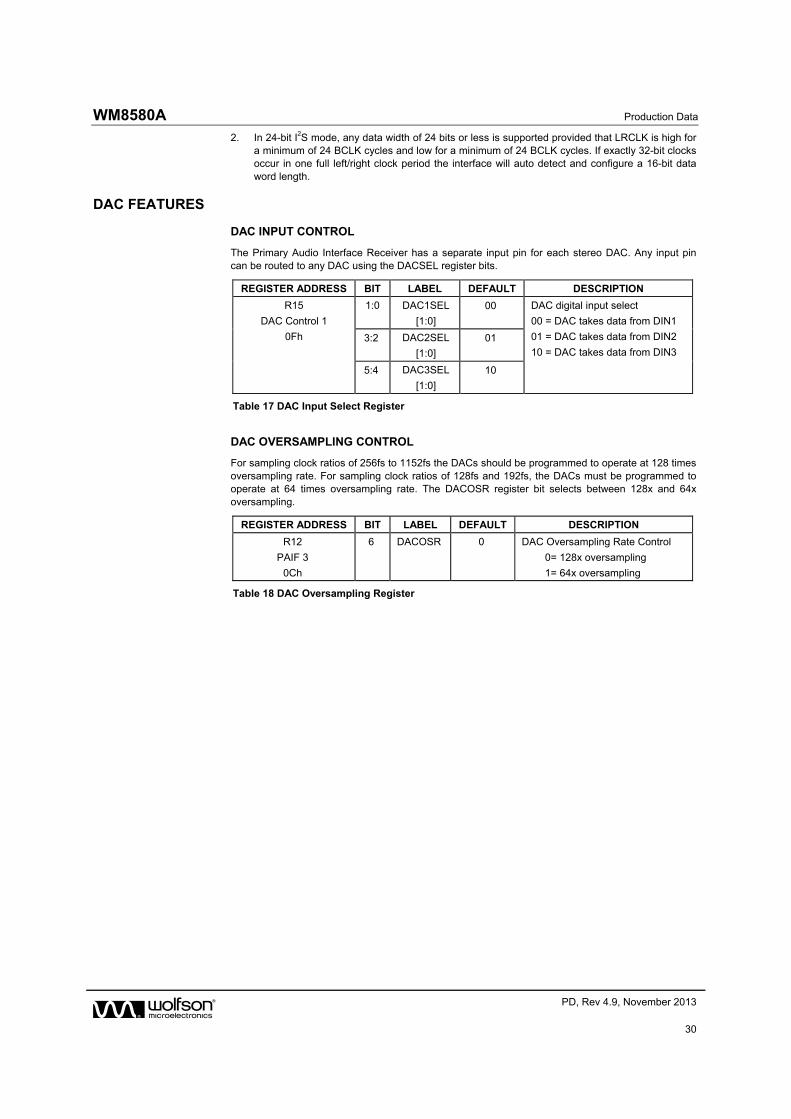
DAC INPUT CONTROL
The Primary Audio Interface Receiver has a separate input pin for each stereo DAC. Any input pin can be routed to any DAC using the DACSEL register bits.
REGISTER ADDRESS BIT LABEL DEFAULT DESCRIPTION
R15
DAC Control 1
0Fh
1:0 DAC1SEL
[1:0]
00 DAC digital input select
00 = DAC takes data from DIN1
01 = DAC takes data from DIN2
10 = DAC takes data from DIN3
3:2 DAC2SEL
[1:0]
01
5:4 DAC3SEL
[1:0]
10
Table 17 DAC Input Select Register
DAC OVERSAMPLING CONTROL
For sampling clock ratios of 256fs to 1152fs the DACs should be programmed to operate at 128 times oversampling rate. For sampling clock ratios of 128fs and 192fs, the DACs must be programmed to operate at 64 times oversampling rate. The DACOSR register bit selects between 128x and 64x oversampling.
REGISTER ADDRESS BIT LABEL DEFAULT DESCRIPTION
R12
PAIF 3
0Ch
6 DACOSR 0 DAC Oversampling Rate Control
0= 128x oversampling
1= 64x oversampling
Table 18 DAC Oversampling Register
Production Data WM8580A
w PD, Rev 4.9, November 2013
31
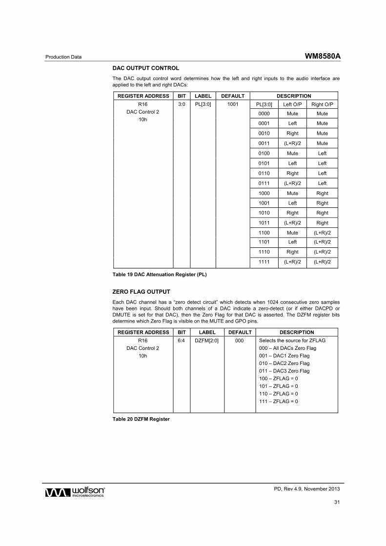
DAC OUTPUT CONTROL
The DAC output control word determines how the left and right inputs to the audio interface are applied to the left and right DACs:
REGISTER ADDRESS BIT LABEL DEFAULT DESCRIPTION
R16
DAC Control 2
10h
3:0 PL[3:0] 1001 PL[3:0] Left O/P Right O/P
0000 Mute Mute
0001 Left Mute
0010 Right Mute
0011 (L+R)/2 Mute
0100 Mute Left
0101 Left Left
0110 Right Left
0111 (L+R)/2 Left
1000 Mute Right
1001 Left Right
1010 Right Right
1011 (L+R)/2 Right
1100 Mute (L+R)/2
1101 Left (L+R)/2
1110 Right (L+R)/2
1111 (L+R)/2 (L+R)/2
Table 19 DAC Attenuation Register (PL)
ZERO FLAG OUTPUT
Each DAC channel has a “zero detect circuit” which detects when 1024 consecutive zero samples have been input. Should both channels of a DAC indicate a zero-detect (or if either DACPD or DMUTE is set for that DAC), then the Zero Flag for that DAC is asserted. The DZFM register bits determine which Zero Flag is visible on the MUTE and GPO pins.
REGISTER ADDRESS BIT LABEL DEFAULT DESCRIPTION
R16
DAC Control 2
10h
6:4 DZFM[2:0] 000 Selects the source for ZFLAG
000 – All DACs Zero Flag
001 – DAC1 Zero Flag
010 – DAC2 Zero Flag
011 – DAC3 Zero Flag
100 – ZFLAG = 0
101 – ZFLAG = 0
110 – ZFLAG = 0
111 – ZFLAG = 0
Table 20 DZFM Register
WM8580A Production Data
w PD, Rev 4.9, November 2013
32
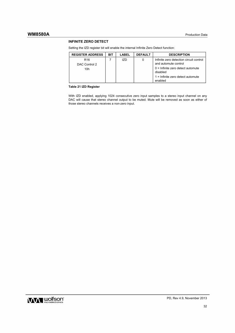
INFINITE ZERO DETECT
Setting the IZD register bit will enable the internal Infinite Zero Detect function:
REGISTER ADDRESS BIT LABEL DEFAULT DESCRIPTION
R16
DAC Control 2
10h
7 IZD 0 Infinite zero detection circuit control and automute control
0 = Infinite zero detect automute disabled
1 = Infinite zero detect automute enabled
Table 21 IZD Register
With IZD enabled, applying 1024 consecutive zero input samples to a stereo input channel on any DAC will cause that stereo channel output to be muted. Mute will be removed as soon as either of those stereo channels receives a non-zero input.
Production Data WM8580A
w PD, Rev 4.9, November 2013
33
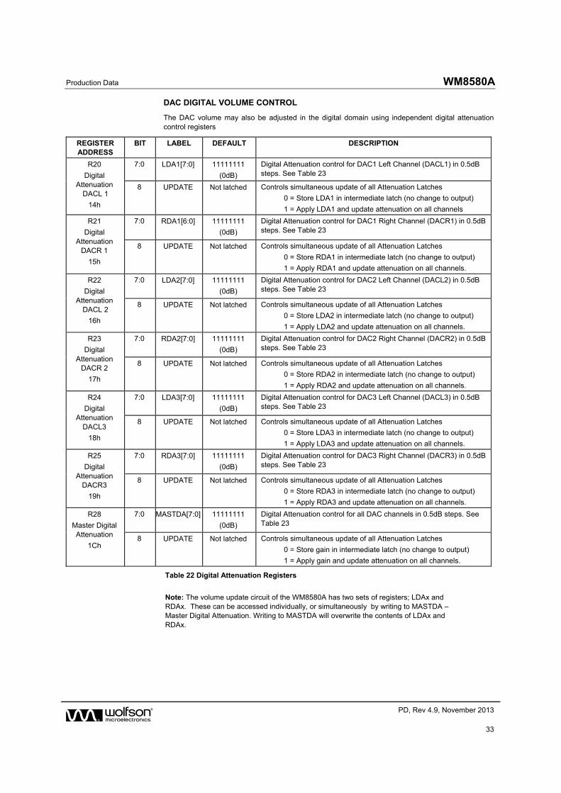
DAC DIGITAL VOLUME CONTROL
The DAC volume may also be adjusted in the digital domain using independent digital attenuation control registers
REGISTER ADDRESS
BIT LABEL DEFAULT DESCRIPTION
R20
Digital Attenuation
DACL 1
14h
7:0 LDA1[7:0] 11111111
(0dB)
Digital Attenuation control for DAC1 Left Channel (DACL1) in 0.5dB steps. See Table 23
8 UPDATE Not latched Controls simultaneous update of all Attenuation Latches
0 = Store LDA1 in intermediate latch (no change to output)
1 = Apply LDA1 and update attenuation on all channels
R21
Digital Attenuation
DACR 1
15h
7:0 RDA1[6:0] 11111111
(0dB)
Digital Attenuation control for DAC1 Right Channel (DACR1) in 0.5dB steps. See Table 23
8 UPDATE Not latched Controls simultaneous update of all Attenuation Latches
0 = Store RDA1 in intermediate latch (no change to output)
1 = Apply RDA1 and update attenuation on all channels.
R22
Digital Attenuation
DACL 2
16h
7:0 LDA2[7:0] 11111111
(0dB)
Digital Attenuation control for DAC2 Left Channel (DACL2) in 0.5dB steps. See Table 23
8 UPDATE Not latched Controls simultaneous update of all Attenuation Latches
0 = Store LDA2 in intermediate latch (no change to output)
1 = Apply LDA2 and update attenuation on all channels.
R23
Digital Attenuation
DACR 2
17h
7:0 RDA2[7:0] 11111111
(0dB)
Digital Attenuation control for DAC2 Right Channel (DACR2) in 0.5dB steps. See Table 23
8 UPDATE Not latched Controls simultaneous update of all Attenuation Latches
0 = Store RDA2 in intermediate latch (no change to output)
1 = Apply RDA2 and update attenuation on all channels.
R24
Digital Attenuation
DACL3
18h
7:0 LDA3[7:0] 11111111
(0dB)
Digital Attenuation control for DAC3 Left Channel (DACL3) in 0.5dB steps. See Table 23
8 UPDATE Not latched Controls simultaneous update of all Attenuation Latches
0 = Store LDA3 in intermediate latch (no change to output)
1 = Apply LDA3 and update attenuation on all channels.
R25
Digital Attenuation
DACR3
19h
7:0 RDA3[7:0] 11111111
(0dB)
Digital Attenuation control for DAC3 Right Channel (DACR3) in 0.5dB steps. See Table 23
8 UPDATE Not latched Controls simultaneous update of all Attenuation Latches
0 = Store RDA3 in intermediate latch (no change to output)
1 = Apply RDA3 and update attenuation on all channels.
R28
Master Digital Attenuation
1Ch
7:0 MASTDA[7:0] 11111111
(0dB)
Digital Attenuation control for all DAC channels in 0.5dB steps. See Table 23
8 UPDATE Not latched Controls simultaneous update of all Attenuation Latches
0 = Store gain in intermediate latch (no change to output)
1 = Apply gain and update attenuation on all channels.
Table 22 Digital Attenuation Registers
Note: The volume update circuit of the WM8580A has two sets of registers; LDAx and RDAx. These can be accessed individually, or simultaneously by writing to MASTDA – Master Digital Attenuation. Writing to MASTDA will overwrite the contents of LDAx and RDAx.
WM8580A Production Data
w PD, Rev 4.9, November 2013
34
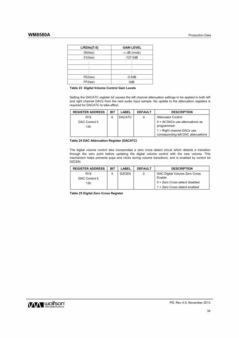
L/RDAx[7:0] GAIN LEVEL
00(hex) - dB (mute)
01(hex) -127.5dB
: :
: :
: :
FE(hex) -0.5dB
FF(hex) 0dB
Table 23 Digital Volume Control Gain Levels
Setting the DACATC register bit causes the left channel attenuation settings to be applied to both left and right channel DACs from the next audio input sample. No update to the attenuation registers is required for DACATC to take effect.
REGISTER ADDRESS BIT LABEL DEFAULT DESCRIPTION
R19
DAC Control 5
13h
6 DACATC 0 Attenuator Control
0 = All DACs use attenuations as programmed.
1 = Right channel DACs use corresponding left DAC attenuations
Table 24 DAC Attenuation Register (DACATC)
The digital volume control also incorporates a zero cross detect circuit which detects a transition through the zero point before updating the digital volume control with the new volume. This mechanism helps prevents pops and clicks during volume transitions, and is enabled by control bit DZCEN.
REGISTER ADDRESS BIT LABEL DEFAULT DESCRIPTION
R19
DAC Control 5
13h
5 DZCEN 0 DAC Digital Volume Zero Cross Enable
0 = Zero Cross detect disabled
1 = Zero Cross detect enabled
Table 25 Digital Zero Cross Register
Production Data WM8580A
w PD, Rev 4.9, November 2013
35
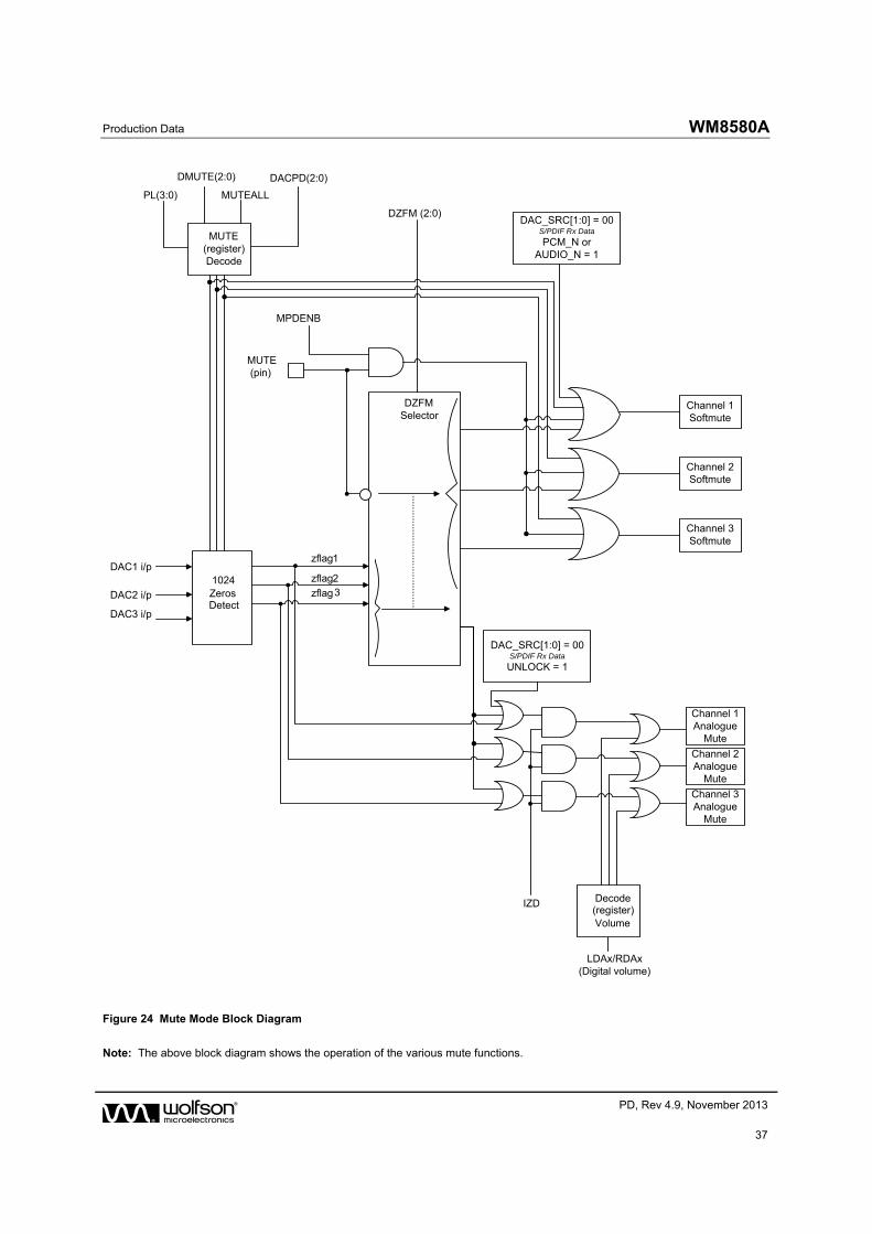
MUTE MODES
The WM8580A has individual mutes for each of the three DAC channels. Setting DMUTE for a channel will apply a ‘soft-mute’ to the input of the digital filters for that channel. DMUTE[0] mutes DAC1 channel, DMUTE[1] mutes DAC2 channel and DMUTE[2] mutes DAC3 channel. Setting the MUTEALL register bit will apply a ‘soft-mute’ to the input of all the DAC digital filters. A soft-mute allows the user to control the analog output of the DAC such that the output waveform is looks like that shown in Figure 23.
The MUTE pin can also be used to apply soft-mute to the DAC selected by the DZFM register bits. However, if the MPDENB register bit is set, the MUTE pin will activate a soft-mute for all DACs.
REGISTER ADDRESS BIT LABEL DEFAULT DESCRIPTION
R19
DAC Control 5
13h
2:0 DMUTE[2:0] 000 DAC channel soft mute enables:
DMUTE[0] = 1, enable soft-mute on DAC1.
DMUTE[1] = 1, enable soft-mute on DAC2.
DMUTE[2] = 1, enable soft-mute on DAC3.
4 MUTEALL 0 DAC channel master soft mute. Mutes all DAC channels:
0 = disable soft-mute on all DACs.
1 = enable soft-mute on all DACs.
7 MPDENB 0 MUTE pin decode enable:
0 = MUTE activates soft-mute on DAC selected by DZFM
1 = MUTE activates softmute on all DACs
Table 26 Mute Registers
WM8580A Production Data
w PD, Rev 4.9, November 2013
36
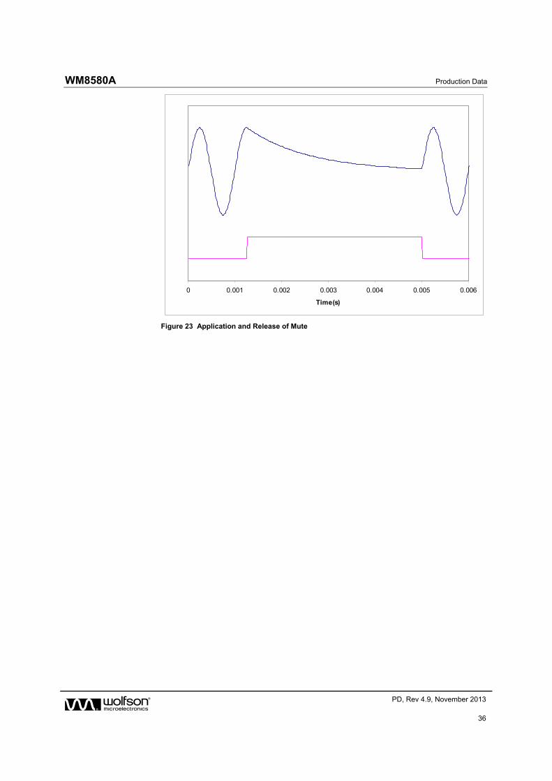
Figure 23 Application and Release of Mute
-2.5
-2
-1.5
-1
-0.5
0
0.5
1
1.5
0 0.001 0.002 0.003 0.004 0.005 0.006
Time(s)
Production Data WM8580A
w PD, Rev 4.9, November 2013
37
DZFMSelector
zflag1
zflag2
zflag3
MUTE(pin)
MUTE(register)Decode
IZD
MPDENB
DMUTE(2:0)
MUTEALL
DAC1 i/p
DAC2 i/p
DAC3 i/p
DZFM (2:0)
1024ZerosDetect
PL(3:0)
DACPD(2:0)
LDAx/RDAx(Digital volume)
Volume(register)Decode
Channel 1Analogue
Mute
Channel 2Analogue
Mute
Channel 3Analogue
Mute
Channel 1Softmute
Channel 2Softmute
Channel 3Softmute
DAC_SRC[1:0] = 00S/PDIF Rx Data
PCM_N orAUDIO_N = 1
DAC_SRC[1:0] = 00S/PDIF Rx Data
UNLOCK = 1
Figure 24 Mute Mode Block Diagram
Note: The above block diagram shows the operation of the various mute functions.
WM8580A Production Data
w PD, Rev 4.9, November 2013
38
Figure 23 shows the application and release of MUTE whilst a full amplitude sinusoid is being played at 48kHz sampling rate. When MUTE (lower trace) is asserted, the output (upper trace) begins to decay exponentially from the DC level of the last input sample. The output will decay towards VMID with a time constant of approximately 64 input samples. If MUTE is applied to all channels for 1024 or more input samples the DAC will be muted if IZD is set. When MUTE is de-asserted, the output will restart immediately from the current input sample.
All other means of muting the DAC channels will cause a much more abrupt muting of the output. This abrupt muting is referred to as an analog mute and it will switch the analog outputs immediately to VMID.
DE-EMPHASIS MODE
A digital de-emphasis filter may be applied to each DAC channel. The de-emphasis filter for each stereo channel is enabled under the control of DEEMP[2:0]. DEEMP[0] enables the de-emphasis filter for DAC 1, DEEMP[1] enables the de-emphasis filter for DAC 2, and DEEMP[2] enables the de-emphasis filter for DAC 3.
REGISTER ADDRESS BIT LABEL DEFAULT DESCRIPTION
R17
DAC Control 3
11h
2:0 DEEMP[2:0] 000 De-emphasis mode select:
DEEMP[0] = 1, enable De-emphasis on DAC1.
DEEMP[1] = 1, enable De-emphasis on DAC2.
DEEMP[2] = 1, enable De-emphasis on DAC3.
4 DEEMPALL 0 0 = De-emphasis controlled by DEEMP[2:0]
1 = De-emphasis enabled on all DACs
Table 27 De-emphasis Register
Refer to Figure 47, Figure 48, Figure 49 and Figure 50 for details of the De-Emphasis modes at different sample rates.
DAC OUTPUT PHASE
The DAC Phase control word determines whether the output of each DAC is non-inverted or inverted
REGISTER ADDRESS BIT LABEL DEFAULT DESCRIPTION
R18
DAC Control 4
12h
5:0 PHASE [5:0]
111111 Controls phase of DAC outputs
0 = inverted
1 = non-inverted
PHASE[0] = 0 inverts phase of DAC1L output
PHASE[1] = 0 inverts phase of DAC1R output
PHASE[2] = 0 inverts phase of DAC2L output
PHASE[3] = 0 inverts phase of DAC2R output
PHASE[4] = 0 inverts phase of DAC3L output
PHASE[5] = 0 inverts phase of DAC3R output
Table 28 DAC Output Phase Register
Production Data WM8580A
w PD, Rev 4.9, November 2013
39
ADC FEATURES
ADC HIGH-PASS FILTER DISABLE
The ADC digital filters incorporate a digital high-pass filter. By default, this is enabled but can be disabled by setting the ADCHPD register bit to 1. This allows the input to the ADC to be DC coupled.
REGISTER ADDRESS BIT LABEL DEFAULT DESCRIPTION
R29
ADC Control 1
1Dh
4 ADCHPD 0 ADC high-pass filter disable
0 = high-pass filter enabled
1 = high-pass filter disabled
Table 29 ADC Functions Register
ADC OVERSAMPLING RATE SELECT
The internal ADC signal processing operates at an oversampling rate of 128fs for all MCLK:LRCLK ratios. The exception to this is for operation with a 128fs or 192fs master clock, where the internal oversampling rate of the ADC is 64fs.
For ADC operation at 96kHz in 256fs or 384fs mode it is recommended that the user set the ADCOSR bit. This changes the ADC signal processing oversampling rate from 128fs to 64fs. Similarly, for ADC operation at 192kHz in 128fs or 192fs mode it is recommended that the user set the ADCOSR bit to change the oversampling rate from 64fs to 32fs.
REGISTER ADDRESS BIT LABEL DEFAULT DESCRIPTION
R29
ADC Control 1
1Dh
3 ADCOSR 0 ADC oversample rate select
0 = 128/64x oversampling
1 = 64/32x oversampling
Table 30 ADC Functions Register
ADC MUTE
As with the DAC, each ADC channel also has a mute control bit, which mutes the inputs to the ADC.
REGISTER ADDRESS
BIT LABEL DEFAULT DESCRIPTION
R29
ADC Control 1
1Dh
0 AMUTEL 0 ADC Mute select
0 : Normal Operation
1: mute ADC left
1 AMUTER 0 ADC Mute select
0 : Normal Operation
1: mute ADC right
2 AMUTEALL 0 ADC Mute select
0 : Normal Operation
1: mute both ADC channels
Table 31 ADC Mute Register
WM8580A Production Data
w PD, Rev 4.9, November 2013
40
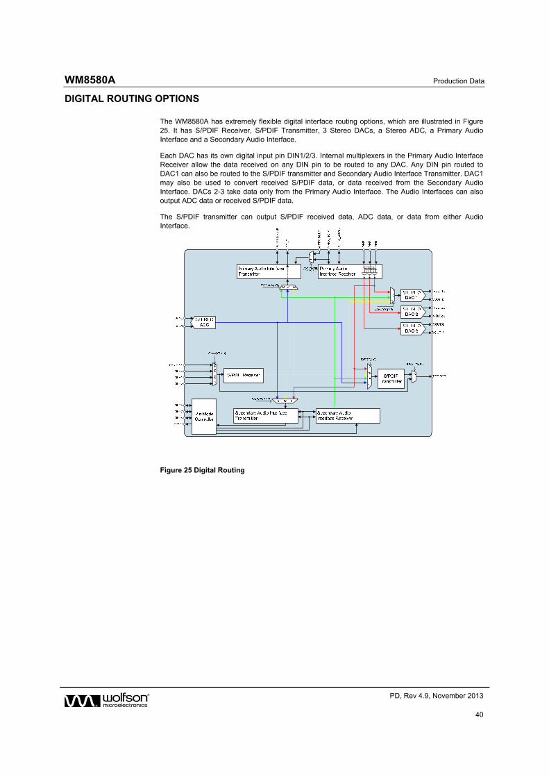
DIGITAL ROUTING OPTIONS
The WM8580A has extremely flexible digital interface routing options, which are illustrated in Figure 25. It has S/PDIF Receiver, S/PDIF Transmitter, 3 Stereo DACs, a Stereo ADC, a Primary Audio Interface and a Secondary Audio Interface.
Each DAC has its own digital input pin DIN1/2/3. Internal multiplexers in the Primary Audio Interface Receiver allow the data received on any DIN pin to be routed to any DAC. Any DIN pin routed to DAC1 can also be routed to the S/PDIF transmitter and Secondary Audio Interface Transmitter. DAC1 may also be used to convert received S/PDIF data, or data received from the Secondary Audio Interface. DACs 2-3 take data only from the Primary Audio Interface. The Audio Interfaces can also output ADC data or received S/PDIF data.
The S/PDIF transmitter can output S/PDIF received data, ADC data, or data from either Audio Interface.
Figure 25 Digital Routing
Production Data WM8580A
w PD, Rev 4.9, November 2013
41
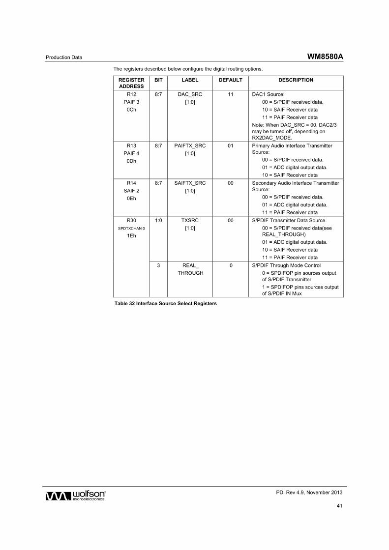
The registers described below configure the digital routing options.
REGISTER ADDRESS
BIT LABEL DEFAULT DESCRIPTION
R12
PAIF 3
0Ch
8:7 DAC_SRC
[1:0]
11 DAC1 Source:
00 = S/PDIF received data.
10 = SAIF Receiver data
11 = PAIF Receiver data
Note: When DAC_SRC = 00, DAC2/3 may be turned off, depending on RX2DAC_MODE.
R13
PAIF 4
0Dh
8:7 PAIFTX_SRC
[1:0]
01 Primary Audio Interface Transmitter Source:
00 = S/PDIF received data.
01 = ADC digital output data.
10 = SAIF Receiver data
R14
SAIF 2
0Eh
8:7 SAIFTX_SRC
[1:0]
00 Secondary Audio Interface Transmitter Source:
00 = S/PDIF received data.
01 = ADC digital output data.
11 = PAIF Receiver data
R30
SPDTXCHAN 0
1Eh
1:0 TXSRC
[1:0]
00 S/PDIF Transmitter Data Source.
00 = S/PDIF received data(see REAL_THROUGH)
01 = ADC digital output data.
10 = SAIF Receiver data
11 = PAIF Receiver data
3 REAL_
THROUGH
0 S/PDIF Through Mode Control
0 = SPDIFOP pin sources output of S/PDIF Transmitter
1 = SPDIFOP pins sources output of S/PDIF IN Mux
Table 32 Interface Source Select Registers
WM8580A Production Data
w PD, Rev 4.9, November 2013
42
CLOCK SELECTION
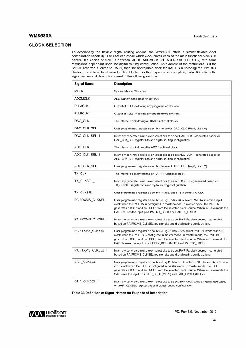
To accompany the flexible digital routing options, the WM8580A offers a similar flexible clock configuration capability. The user can chose which clock drives each of the main functional blocks. In general the choice of clock is between MCLK, ADCMCLK, PLLACLK and PLLBCLK, with some restrictions dependant upon the digital routing configuration. An example of the restrictions is if the S/PDIF receiver is routed to DAC1, then the appropriate clock for DAC1 is autoconfigured. Not all 4 clocks are available to all main function blocks. For the purposes of description, Table 33 defines the signal names and descriptions used in the following sections.
Signal Name Description
MCLK System Master Clock pin
ADCMCLK ADC Masetr clock input pin (MFP2)
PLLACLK Output of PLLA (following any programmed division)
PLLBCLK Output of PLLB (following any programmed division)
DAC_CLK The internal clock driving all DAC functional blocks
DAC_CLK_SEL User programmed register select bits to select DAC_CLK (Reg8, bits 1:0)
DAC_CLK_SEL_I Internally generated multiplexer select bits to select DAC_CLK – generated based on
DAC_CLK_SEL register bits and digital routing configuration.
ADC_CLK The internal clock driving the ADC functional block
ADC_CLK_SEL_I Internally generated multiplexer select bits to select ADC_CLK – generated based on
ADC_CLK_SEL register bits and digital routing configuration.
ADC_CLK_SEL User programmed register select bits to select ADC_CLK (Reg8, bits 3:2)
TX_CLK The internal clock driving the S/PDIF Tx functional block
TX_CLKSEL_I Internally generated multiplexer select bits to select TX_CLK – generated based on
TX_CLKSEL register bits and digital routing configuration.
TX_CLKSEL User programmed register select bits (Reg8, bits 5:4) to select TX_CLK
PAIFRXMS_CLKSEL User programmed register select bits (Reg9, bits 7:6) to select PAIF Rx interface input
clock when the PAIF Rx is configured in master mode. In master mode, the PAIF Rx
generates a BCLK and an LRCLK from the selected clock source. When in Slave mode the
PAIF Rx uses the input pins PAIFRX_BCLK and PAIFRX_LRCLK
PAIFRXMS_CLKSEL_I Internally generated multiplexer select bits to select PAIF Rx clock source – generated
based on PAIFRXMS_CLKSEL register bits and digital routing configuration.
PAIFTXMS_CLKSEL User programmed register select bits (Reg??, bits ??) to select PAIF Tx interface input
clock when the PAIF Tx is configured in master mode. In master mode, the PAIF Tx
generates a BCLK and an LRCLK from the selected clock source. When in Slave mode the
PAIF Tx uses the input pins PAIFTX_BCLK (MFP1) and PAIFTX_LRCLK
PAIFTXMS_CLKSEL_I Internally generated multiplexer select bits to select PAIF Rx clock source – generated
based on PAIFRXMS_CLKSEL register bits and digital routing configuration.
SAIF_CLKSEL User programmed register select bits (Reg11, bits 7:6) to select SAIF (Tx and Rx) interface
input clock when the SAIF is configured in master mode. In master mode, the SAIF
generates a BCLK and an LRCLK from the selected clock source. When in Slave mode the
SAIF uses the input pins SAIF_BCLK (MFP6) and SAIF_LRCLK (MFP7).
SAIF_CLKSEL_I Internally generated multiplexer select bits to select SAIF clock source – generated based
on SAIF_CLKSEL register bits and digital routing configuration.
Table 33 Definition of Signal Names for Purpose of Description
Production Data WM8580A
w PD, Rev 4.9, November 2013
43
It is possible to override any autoconfiguration of clocks, allowing the user to manually select an available clock for a particular interface using the appropriate CLKSEL register bits. The autoconfiguration can be overridden using the CLKSEL_MAN bit (Reg6, bit 6). Great care must to used when overriding autoconfigured clocking.This is described in Manual Clock Selection section.
The sample rate at which the DAC, ADC and S/PDIF interfaces operate is configurable. The rate of operation is determined by the available LRCLK at the interface and how the interface is configured – master or slave mode. The available options are described in the sections which follow.
The PAIF and SAIF generate a BLCK and LRCLK if in master mode. In slave mode they use the clocks from input pins.
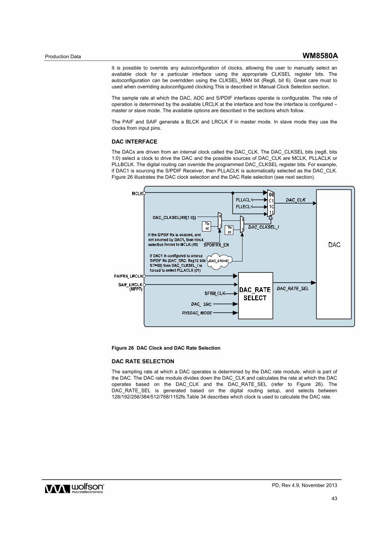
DAC INTERFACE
The DACs are driven from an internal clock called the DAC_CLK. The DAC_CLKSEL bits (reg8, bits 1:0) select a clock to drive the DAC and the possible sources of DAC_CLK are MCLK, PLLACLK or PLLBCLK. The digital routing can override the programmed DAC_CLKSEL register bits. For example, if DAC1 is sourcing the S/PDIF Receiver, then PLLACLK is automatically selected as the DAC_CLK. Figure 26 illustrates the DAC clock selection and the DAC Rate selection (see next section).
Figure 26 DAC Clock and DAC Rate Selection
DAC RATE SELECTION
The sampling rate at which a DAC operates is determined by the DAC rate module, which is part of the DAC. The DAC rate module divides down the DAC_CLK and calculates the rate at which the DAC operates based on the DAC_CLK and the DAC_RATE_SEL (refer to Figure 26). The DAC_RATE_SEL is generated based on the digital routing setup, and selects between 128/192/256/384/512/768/1152fs.Table 34 describes which clock is used to calculate the DAC rate.
WM8580A Production Data
w PD, Rev 4.9, November 2013
44
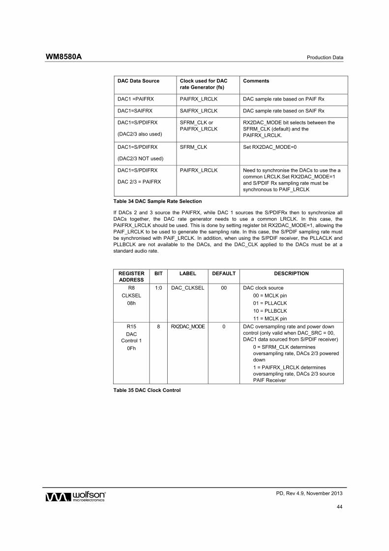
DAC Data Source Clock used for DAC rate Generator (fs)
Comments
DAC1 =PAIFRX PAIFRX_LRCLK DAC sample rate based on PAIF Rx
DAC1=SAIFRX SAIFRX_LRCLK DAC sample rate based on SAIF Rx
DAC1=S/PDIFRX
(DAC2/3 also used)
SFRM_CLK or PAIFRX_LRCLK
RX2DAC_MODE bit selects between the SFRM_CLK (default) and the PAIFRX_LRCLK.
DAC1=S/PDIFRX
(DAC2/3 NOT used)
SFRM_CLK Set RX2DAC_MODE=0
DAC1=S/PDIFRX
DAC 2/3 = PAIFRX
PAIFRX_LRCLK Need to synchronise the DACs to use the a common LRCLK.Set RX2DAC_MODE=1 and S/PDIF Rx sampling rate must be synchronous to PAIF_LRCLK
Table 34 DAC Sample Rate Selection
If DACs 2 and 3 source the PAIFRX, while DAC 1 sources the S/PDIFRx then to synchronize all DACs together, the DAC rate generator needs to use a common LRCLK. In this case, the PAIFRX_LRCLK should be used. This is done by setting register bit RX2DAC_MODE=1, allowing the PAIF_LRCLK to be used to generate the sampling rate. In this case, the S/PDIF sampling rate must be synchronised with PAIF_LRCLK. In addition, when using the S/PDIF receiver, the PLLACLK and PLLBCLK are not available to the DACs, and the DAC_CLK applied to the DACs must be at a standard audio rate.
REGISTER ADDRESS
BIT LABEL DEFAULT DESCRIPTION
R8
CLKSEL
08h
1:0 DAC_CLKSEL 00 DAC clock source
00 = MCLK pin
01 = PLLACLK
10 = PLLBCLK
11 = MCLK pin
R15
DAC Control 1
0Fh
8 RX2DAC_MODE 0 DAC oversampling rate and power down control (only valid when DAC_SRC = 00, DAC1 data sourced from S/PDIF receiver)
0 = SFRM_CLK determines oversampling rate, DACs 2/3 powered down
1 = PAIFRX_LRCLK determines oversampling rate, DACs 2/3 source PAIF Receiver
Table 35 DAC Clock Control
Production Data WM8580A
w PD, Rev 4.9, November 2013
45
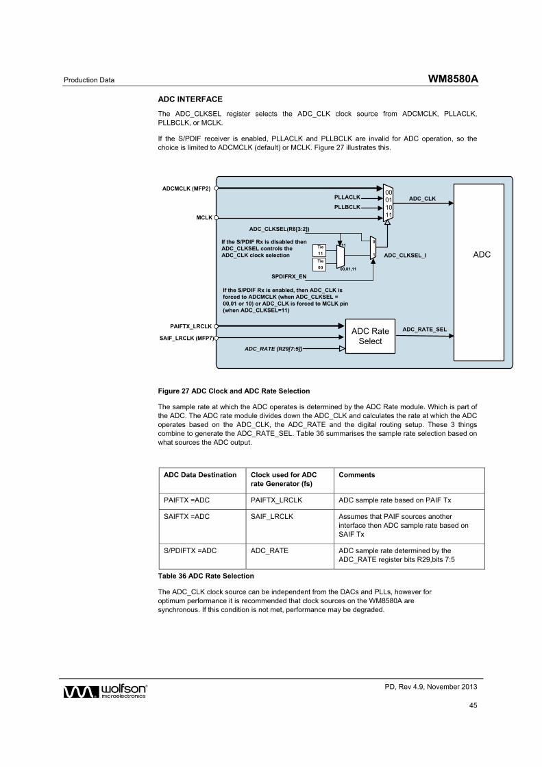
ADC INTERFACE
The ADC_CLKSEL register selects the ADC_CLK clock source from ADCMCLK, PLLACLK, PLLBCLK, or MCLK.
If the S/PDIF receiver is enabled, PLLACLK and PLLBCLK are invalid for ADC operation, so the choice is limited to ADCMCLK (default) or MCLK. Figure 27 illustrates this.
00011011MCLK
ADCMCLK (MFP2)
PLLACLK
PLLBCLK
ADC
ADC RateSelect
ADC_RATE (R29[7:5])
PAIFTX_LRCLK
SAIF_LRCLK (MFP7)
ADC_CLK
0
1
Tie
11
11
00,01,11
Tie
00
ADC_CLKSEL(R8[3:2])
SPDIFRX_EN
ADC_CLKSEL_I
If the S/PDIF Rx is enabled, then ADC_CLK is forced to ADCMCLK (when ADC_CLKSEL = 00,01 or 10) or ADC_CLK is forced to MCLK pin (when ADC_CLKSEL=11)
If the S/PDIF Rx is disabled then ADC_CLKSEL controls the ADC_CLK clock selection
ADC_RATE_SEL
Figure 27 ADC Clock and ADC Rate Selection
The sample rate at which the ADC operates is determined by the ADC Rate module. Which is part of the ADC. The ADC rate module divides down the ADC_CLK and calculates the rate at which the ADC operates based on the ADC_CLK, the ADC_RATE and the digital routing setup. These 3 things combine to generate the ADC_RATE_SEL. Table 36 summarises the sample rate selection based on what sources the ADC output.
ADC Data Destination Clock used for ADC rate Generator (fs)
Comments
PAIFTX =ADC PAIFTX_LRCLK ADC sample rate based on PAIF Tx
SAIFTX =ADC SAIF_LRCLK Assumes that PAIF sources another interface then ADC sample rate based on SAIF Tx
S/PDIFTX =ADC ADC_RATE ADC sample rate determined by the ADC_RATE register bits R29,bits 7:5
Table 36 ADC Rate Selection
The ADC_CLK clock source can be independent from the DACs and PLLs, however for optimum performance it is recommended that clock sources on the WM8580A are synchronous. If this condition is not met, performance may be degraded.
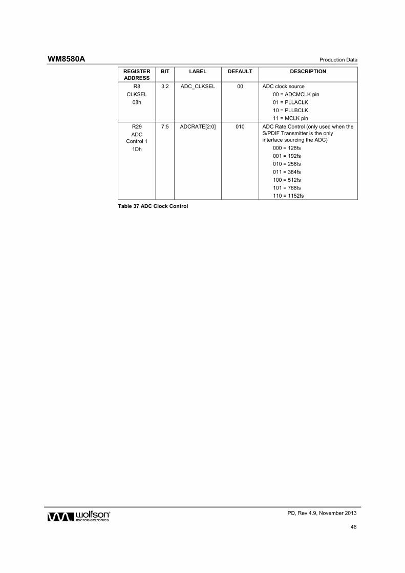
WM8580A Production Data
w PD, Rev 4.9, November 2013
46
REGISTER ADDRESS
BIT LABEL DEFAULT DESCRIPTION
R8
CLKSEL
08h
3:2 ADC_CLKSEL 00 ADC clock source
00 = ADCMCLK pin
01 = PLLACLK
10 = PLLBCLK
11 = MCLK pin
R29
ADC Control 1
1Dh
7:5 ADCRATE[2:0] 010 ADC Rate Control (only used when the S/PDIF Transmitter is the only interface sourcing the ADC)
000 = 128fs
001 = 192fs
010 = 256fs
011 = 384fs
100 = 512fs
101 = 768fs
110 = 1152fs
Table 37 ADC Clock Control
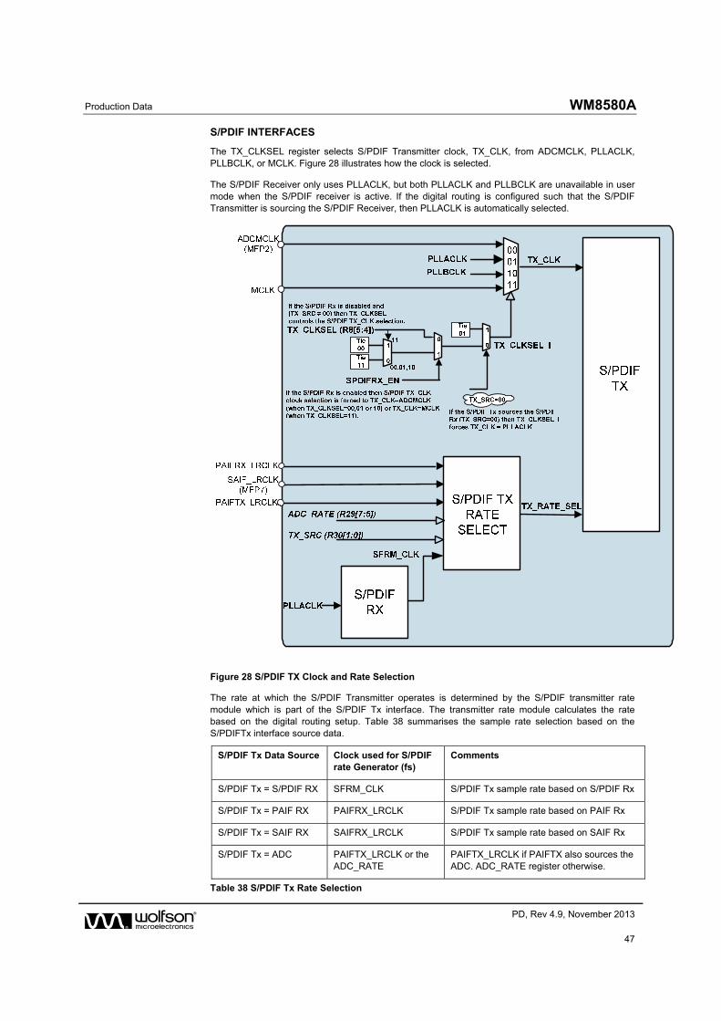
Production Data WM8580A
w PD, Rev 4.9, November 2013
47
S/PDIF INTERFACES
The TX_CLKSEL register selects S/PDIF Transmitter clock, TX_CLK, from ADCMCLK, PLLACLK, PLLBCLK, or MCLK. Figure 28 illustrates how the clock is selected.
The S/PDIF Receiver only uses PLLACLK, but both PLLACLK and PLLBCLK are unavailable in user mode when the S/PDIF receiver is active. If the digital routing is configured such that the S/PDIF Transmitter is sourcing the S/PDIF Receiver, then PLLACLK is automatically selected.
Figure 28 S/PDIF TX Clock and Rate Selection
The rate at which the S/PDIF Transmitter operates is determined by the S/PDIF transmitter rate module which is part of the S/PDIF Tx interface. The transmitter rate module calculates the rate based on the digital routing setup. Table 38 summarises the sample rate selection based on the S/PDIFTx interface source data.
S/PDIF Tx Data Source Clock used for S/PDIF rate Generator (fs)
Comments
S/PDIF Tx = S/PDIF RX SFRM_CLK S/PDIF Tx sample rate based on S/PDIF Rx
S/PDIF Tx = PAIF RX PAIFRX_LRCLK S/PDIF Tx sample rate based on PAIF Rx
S/PDIF Tx = SAIF RX SAIFRX_LRCLK S/PDIF Tx sample rate based on SAIF Rx
S/PDIF Tx = ADC PAIFTX_LRCLK or the ADC_RATE
PAIFTX_LRCLK if PAIFTX also sources the ADC. ADC_RATE register otherwise.
Table 38 S/PDIF Tx Rate Selection
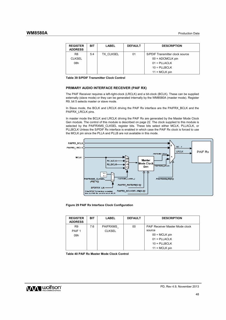
WM8580A Production Data
w PD, Rev 4.9, November 2013
48
REGISTER ADDRESS
BIT LABEL DEFAULT DESCRIPTION
R8
CLKSEL
08h
5:4 TX_CLKSEL 01 S/PDIF Transmitter clock source
00 = ADCMCLK pin
01 = PLLACLK
10 = PLLBCLK
11 = MCLK pin
Table 39 S/PDIF Transmitter Clock Control
PRIMARY AUDIO INTERFACE RECEIVER (PAIF RX)
The PAIF Receiver requires a left-right-clock (LRCLK) and a bit-clock (BCLK). These can be supplied externally (slave mode) or they can be generated internally by the WM8580A (master mode). Register R9, bit 5 selects master or slave mode.
In Slave mode, the BCLK and LRCLK driving the PAIF Rx interface are the PAIFRX_BCLK and the PAIFRX_LRCLK pins.
In master mode the BCLK and LRCLK driving the PAIF Rx are generated by the Master Mode Clock Gen module. The control of this module is described on page 22. The clock supplied to this module is selected by the PAIFRXMS_CLKSEL register bits. These bits select either MCLK, PLLACLK, or PLLBCLK Unless the S/PDIF Rx interface is enabled in which case the PAIF Rx clock is forced to use the MCLK pin since the PLLA and PLLB are not available in this mode.
Figure 29 PAIF Rx Interface Clock Configuration
REGISTER ADDRESS
BIT LABEL DEFAULT DESCRIPTION
R9
PAIF 1
09h
7:6 PAIFRXMS_
CLKSEL
00 PAIF Receiver Master Mode clock source
00 = MCLK pin
01 = PLLACLK
10 = PLLBCLK
11 = MCLK pin
Table 40 PAIF Rx Master Mode Clock Control
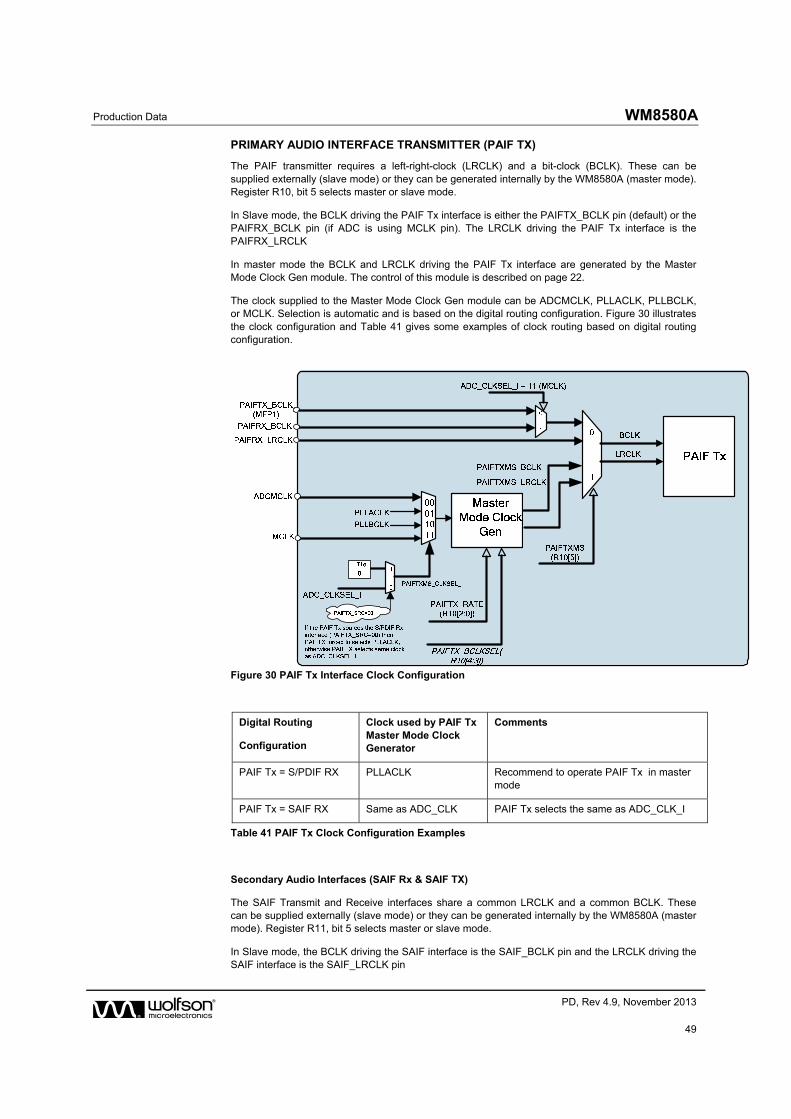
Production Data WM8580A
w PD, Rev 4.9, November 2013
49
PRIMARY AUDIO INTERFACE TRANSMITTER (PAIF TX)
The PAIF transmitter requires a left-right-clock (LRCLK) and a bit-clock (BCLK). These can be supplied externally (slave mode) or they can be generated internally by the WM8580A (master mode). Register R10, bit 5 selects master or slave mode.
In Slave mode, the BCLK driving the PAIF Tx interface is either the PAIFTX_BCLK pin (default) or the PAIFRX_BCLK pin (if ADC is using MCLK pin). The LRCLK driving the PAIF Tx interface is the PAIFRX_LRCLK
In master mode the BCLK and LRCLK driving the PAIF Tx interface are generated by the Master Mode Clock Gen module. The control of this module is described on page 22.
The clock supplied to the Master Mode Clock Gen module can be ADCMCLK, PLLACLK, PLLBCLK, or MCLK. Selection is automatic and is based on the digital routing configuration. Figure 30 illustrates the clock configuration and Table 41 gives some examples of clock routing based on digital routing configuration.
Figure 30 PAIF Tx Interface Clock Configuration
Digital Routing
Configuration
Clock used by PAIF Tx Master Mode Clock Generator
Comments
PAIF Tx = S/PDIF RX PLLACLK Recommend to operate PAIF Tx in master mode
PAIF Tx = SAIF RX Same as ADC_CLK PAIF Tx selects the same as ADC_CLK_I
Table 41 PAIF Tx Clock Configuration Examples
Secondary Audio Interfaces (SAIF Rx & SAIF TX)
The SAIF Transmit and Receive interfaces share a common LRCLK and a common BCLK. These can be supplied externally (slave mode) or they can be generated internally by the WM8580A (master mode). Register R11, bit 5 selects master or slave mode.
In Slave mode, the BCLK driving the SAIF interface is the SAIF_BCLK pin and the LRCLK driving the SAIF interface is the SAIF_LRCLK pin
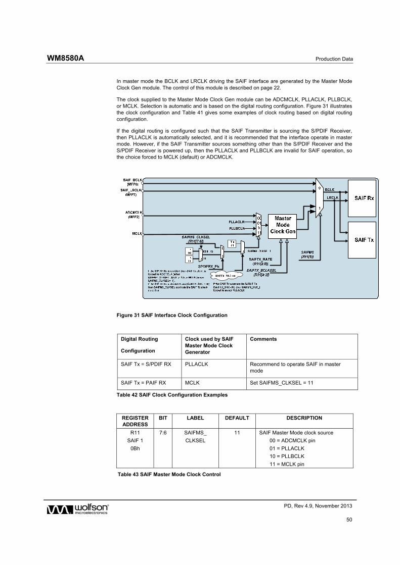
WM8580A Production Data
w PD, Rev 4.9, November 2013
50
In master mode the BCLK and LRCLK driving the SAIF interface are generated by the Master Mode Clock Gen module. The control of this module is described on page 22.
The clock supplied to the Master Mode Clock Gen module can be ADCMCLK, PLLACLK, PLLBCLK, or MCLK. Selection is automatic and is based on the digital routing configuration. Figure 31 illustrates the clock configuration and Table 41 gives some examples of clock routing based on digital routing configuration.
If the digital routing is configured such that the SAIF Transmitter is sourcing the S/PDIF Receiver, then PLLACLK is automatically selected, and it is recommended that the interface operate in master mode. However, if the SAIF Transmitter sources something other than the S/PDIF Receiver and the S/PDIF Receiver is powered up, then the PLLACLK and PLLBCLK are invalid for SAIF operation, so the choice forced to MCLK (default) or ADCMCLK.
Figure 31 SAIF Interface Clock Configuration
Digital Routing
Configuration
Clock used by SAIF Master Mode Clock Generator
Comments
SAIF Tx = S/PDIF RX PLLACLK Recommend to operate SAIF in master mode
SAIF Tx = PAIF RX MCLK Set SAIFMS_CLKSEL = 11
Table 42 SAIF Clock Configuration Examples
REGISTER ADDRESS
BIT LABEL DEFAULT DESCRIPTION
R11
SAIF 1
0Bh
7:6 SAIFMS_
CLKSEL
11 SAIF Master Mode clock source
00 = ADCMCLK pin
01 = PLLACLK
10 = PLLBCLK
11 = MCLK pin
Table 43 SAIF Master Mode Clock Control
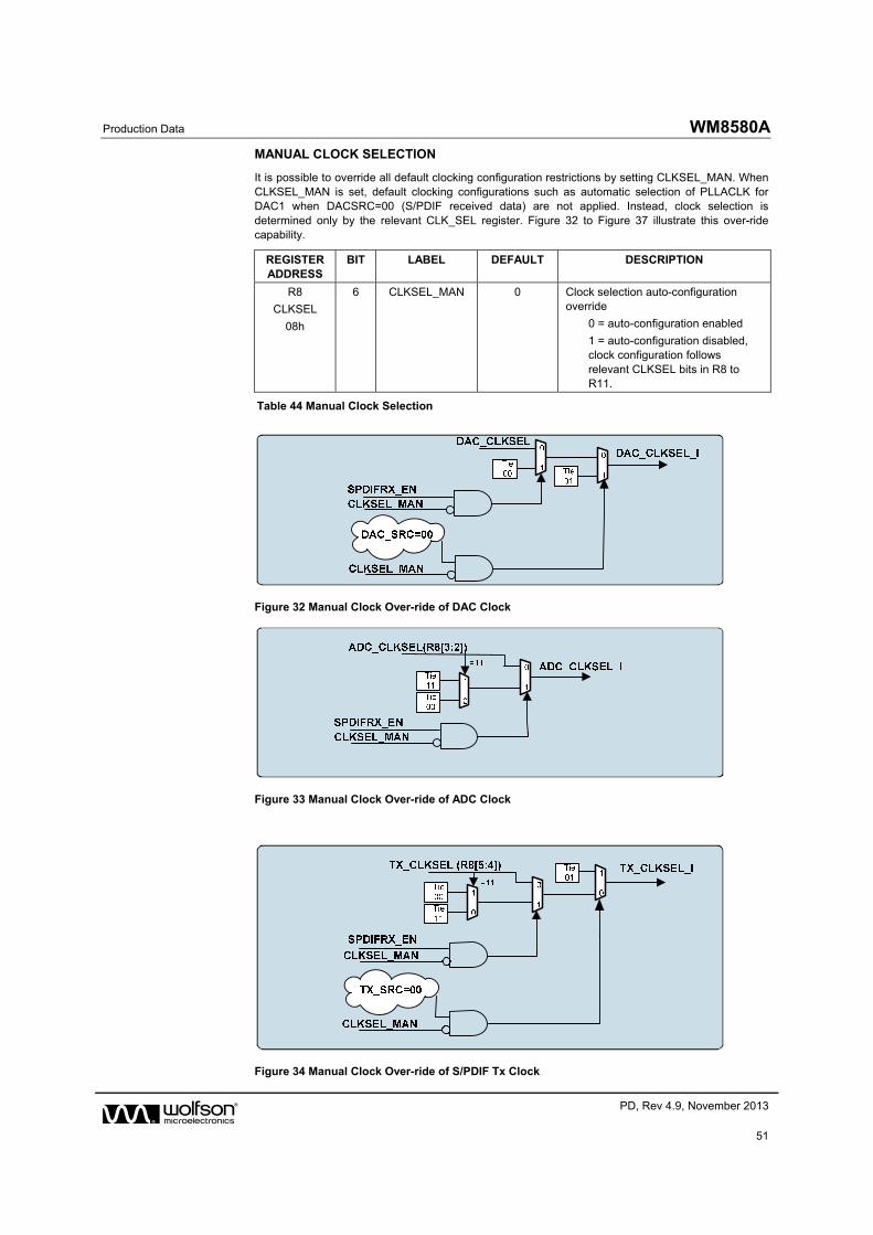
Production Data WM8580A
w PD, Rev 4.9, November 2013
51
MANUAL CLOCK SELECTION
It is possible to override all default clocking configuration restrictions by setting CLKSEL_MAN. When CLKSEL_MAN is set, default clocking configurations such as automatic selection of PLLACLK for DAC1 when DACSRC=00 (S/PDIF received data) are not applied. Instead, clock selection is determined only by the relevant CLK_SEL register. Figure 32 to Figure 37 illustrate this over-ride capability.
REGISTER ADDRESS
BIT LABEL DEFAULT DESCRIPTION
R8
CLKSEL
08h
6 CLKSEL_MAN 0 Clock selection auto-configuration override
0 = auto-configuration enabled
1 = auto-configuration disabled, clock configuration follows relevant CLKSEL bits in R8 to R11.
Table 44 Manual Clock Selection
Figure 32 Manual Clock Over-ride of DAC Clock
Figure 33 Manual Clock Over-ride of ADC Clock
Figure 34 Manual Clock Over-ride of S/PDIF Tx Clock
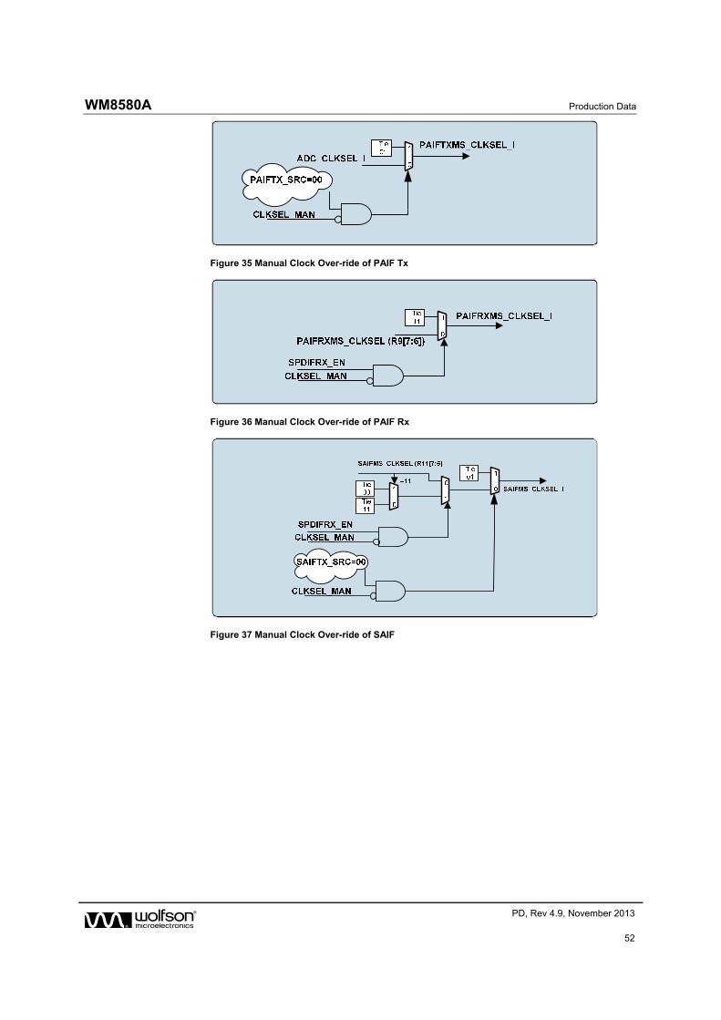
WM8580A Production Data
w PD, Rev 4.9, November 2013
52
Figure 35 Manual Clock Over-ride of PAIF Tx
Figure 36 Manual Clock Over-ride of PAIF Rx
Figure 37 Manual Clock Over-ride of SAIF
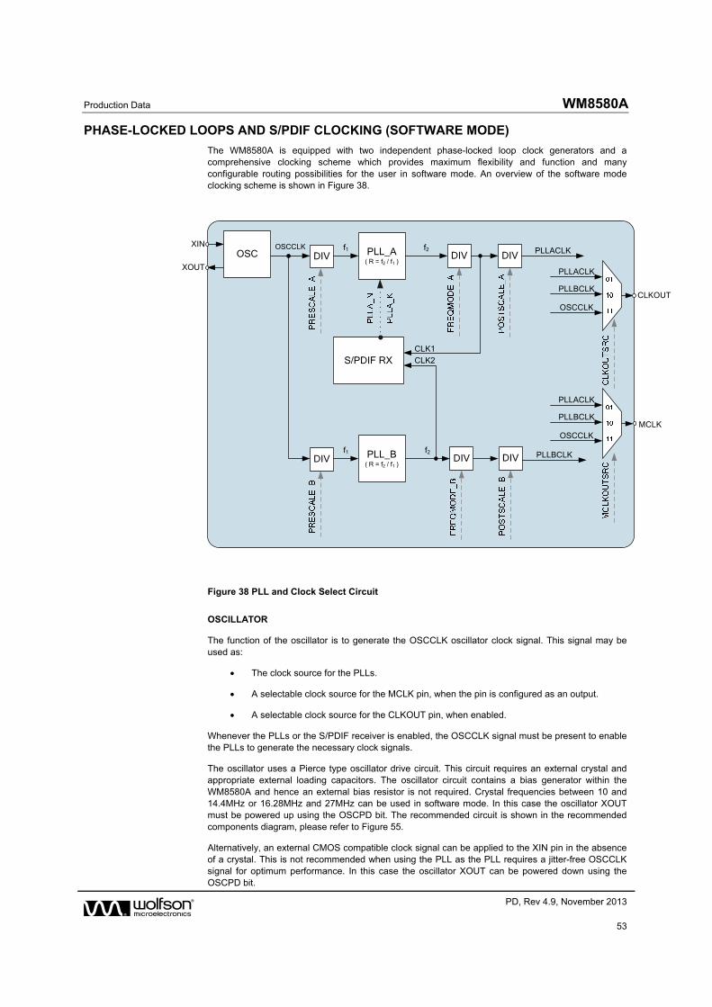
Production Data WM8580A
w PD, Rev 4.9, November 2013
53
PHASE-LOCKED LOOPS AND S/PDIF CLOCKING (SOFTWARE MODE)
The WM8580A is equipped with two independent phase-locked loop clock generators and a comprehensive clocking scheme which provides maximum flexibility and function and many configurable routing possibilities for the user in software mode. An overview of the software mode clocking scheme is shown in Figure 38.
PLL_A( R = f2 / f1 )
DIV DIVf1OSCCLK f2
DIV PLLACLKOSC
CLKOUT
XOUT
XIN
S/PDIF RX
PLL_B( R = f2 / f1 )
DIVf1 f2
DIV DIV PLLBCLK
PLLBCLK
OSCCLK
PLLACLK
MCLKPLLBCLK
OSCCLK
PLLACLK
CLK2
CLK1
Figure 38 PLL and Clock Select Circuit
OSCILLATOR
The function of the oscillator is to generate the OSCCLK oscillator clock signal. This signal may be used as:
The clock source for the PLLs.
A selectable clock source for the MCLK pin, when the pin is configured as an output.
A selectable clock source for the CLKOUT pin, when enabled.
Whenever the PLLs or the S/PDIF receiver is enabled, the OSCCLK signal must be present to enable the PLLs to generate the necessary clock signals.
The oscillator uses a Pierce type oscillator drive circuit. This circuit requires an external crystal and appropriate external loading capacitors. The oscillator circuit contains a bias generator within the WM8580A and hence an external bias resistor is not required. Crystal frequencies between 10 and 14.4MHz or 16.28MHz and 27MHz can be used in software mode. In this case the oscillator XOUT must be powered up using the OSCPD bit. The recommended circuit is shown in the recommended components diagram, please refer to Figure 55.
Alternatively, an external CMOS compatible clock signal can be applied to the XIN pin in the absence of a crystal. This is not recommended when using the PLL as the PLL requires a jitter-free OSCCLK signal for optimum performance. In this case the oscillator XOUT can be powered down using the OSCPD bit.
WM8580A Production Data
w PD, Rev 4.9, November 2013
54
The oscillator XOUT pin has one control bit as shown in Table 45.
REGISTER ADDRESS
BIT LABEL DEFAULT DESCRIPTION
R51
PWRDN 2
33h
0 OSCPD 0 Oscillator XOUT Power Down
0 = Power Up XOUT (crystal mode)
1 = Power Down XOUT (CMOS clock input mode)
Table 45 Oscillator Control
PHASE-LOCKED LOOP (PLL)
The WM8580A has two on-chip phase-locked loop (PLL) circuits which can be used to synthesise two independent clock signals (PLLACLK and PLLBCLK) from the external oscillator clock. The PLLs can be used to:
Generate clocks necessary for the S/PDIF receiver to lock on to and recover S/PDIF data from an incoming S/PDIF data stream.
Generate clocks which may be used to drive the MCLK and/or CLKOUT pins.
Generate clocks which may be used by the S/PDIF transmitter to encode and transmit a S/PDIF data stream.
Generate clocks which may be used as the master clock source for the the ADC and DACs.
Generate clocks which may be used by the master mode clock generator to generate the BCLK and LRCLK signals for the digital audio interfaces.
The PLLs can be enabled or disabled using the register bits shown in Table 46.
REGISTER ADDRESS
BIT LABEL DEFAULT DESCRIPTION
R51
PWRDN 2
33h
1 PLLAPD 1 PLL Power Down Control
0 = Power Up PLL
1 = Power Down PLL
2 PLLBPD 1
Table 46 PLL Power Down Control
The PLLs have two modes of operation:
PLL S/PDIF Receive Mode (Selected if S/PDIF Receiver Enabled)
In S/PDIF receive mode, PLLA is automatically controlled by the S/PDIF receiver to allow the receiver to use PLLA to track and lock on to the incoming S/PDIF data stream. In this case, CLK1 is automatically maintained at a constant frequency of 256fs relative to the sample rate of the recovered S/PDIF stream. PLLB must be configured to produce CLK2, a specific reference clock for the S/PDIF receiver.
PLLACLK may be used as a 256fs or 128fs (selectable – refer to Table 51) master clock source when in S/PDIF receiver mode. PLLBCLK is not available and must not be selected as the clock source for any internal function when the S/PDIF receiver is enabled.
If the sample frequency of the incoming stream is changed and PLLA is forced to unlock in order to track to the new sample frequency, the PLLACLK signal will be stopped until the S/PDIF receiver has locked to the incoming stream at the new sample frequency. If the incoming S/PDIF stream stops, the PLLA_ N and PLLA_K values will be frozen and the PLLACLK will continue at the frequency set by the last recovered S/PDIF stream.
Refer to Table 47 and Table 49 for details of the registers available for configuration in this mode. Refer to the S/PDIF Receive Mode Clocking section on page 59 for full details.
Production Data WM8580A
w PD, Rev 4.9, November 2013
55
PLL User Mode (Selected if S/PDIF Receiver Disabled)
In user mode, the user has full control over the function and operation of both PLLA and PLLB. In this mode, the user can accurately specify the PLL N and K multiplier values and the pre and post-scale divider values and can hence fully control the generated clock frequencies.
Refer to Table 47 and Table 49 for details of the registers available for configuration in this mode.
REGISTER ADDRESS
BIT LABEL DEFAULT DESCRIPTION
R0
PLLA 1/
DEVID1
00h
8:0 PLLA_K[8:0] 100100001 Fractional (K) part of PLLA frequency ratio II .
Value K is one 22-digit binary number spread over registers R0, R1 and R2 as shown.
R1
PLLA 2/
DEVID2
01h
8:0 PLLA_K[17:9] 101111110
R2
PLLA 3/
DEVREV
02h
3:0 PLLA_K[21:18] 1101
7:4 PLLA_N[3:0] 0111 Integer (N) part of PLLA frequency ratio. I
Use values in the range 5 ≤ PLLA_N ≤ 13 as close as possible to 8
R4
PLLB 1
04h
8:0 PLLB_K[8:0] 100100001 Fractional (K) part of PLLB frequency ratio I.
Value K is one 22-digit binary number spread over registers R4, R5 and R6 as shown.
Note: PLLB_K must be set to specific values when the S/PDIF receiver is used. Refer to S/PDIF Receive Mode Clocking section for details.
R5
PLLB 2
05h
8:0 PLLB_K[17:9] 101111110
R6
PLLB 3
06h
3:0 PLLB_K[21:18] 1101
7:4 PLLB_N[3:0] 0111 Integer (N) part of PLLB frequency rat atioII(R).
Use values in the range 5 ≤ PLLB_N ≤ 13 as close as possible to 8
Note: PLLB_N must be set to specific values when the S/PDIF receiver is used. Refer to S/PDIF Receive Mode Clocking section for details.
Table 47 User Mode PLL_K and PLL_N Multiplier Control
PARAMETER PLL USER
MODE PLL S/PDIF RECEIVER MODE
PRESCALE_A Manual Write PRESCALE_B Value
PRESCALE_B Manual Configure Specified PLLB Frequency
PLLA_N Manual Automatically Controlled
PLLA_K Manual Automatically Controlled
PLLB_N Manual Configure Specified PLLB Frequency
PLLB_K Manual Configure Specified PLLB Frequency
FREQMODE_A Manual Automatically Controlled
FREQMODE_B Manual Not Used
POSTSCALE_A Manual 256fs/128fs PLLACLK Select
POSTSCALE_B Manual Not Used
Table 48 PLL Control Register Function in PLL User and PLL S/PDIF Receiver Modes
WM8580A Production Data
w PD, Rev 4.9, November 2013
56
PLL CONFIGURATION
The PLLs perform a configurable frequency multiplication of the input clock signal (f1). The multiplication factor of the PLL (denoted by ‘R’) is variable and is defined by the relationship: R = (f2 ÷ f1).
The multiplication factor for each PLL is set using register bits PLLx_N and PLLx_K (refer to Table 47). The multiplication effect of both the N and K multipliers are additive (i.e. if N is configured to provide a multiplication factor of 8 and K is configured to provide a multiplication factor of 0.192, the overall multiplication factor is 8 + 0.192 = 8.192).
In order to choose and configure the correct values for PLLx_N and PLLx_K, multiplication factor R must first be calculated. Once value R is calculated, the value of PLLx_N is the integer (whole number) value of R, ignoring all digits to the right of the decimal point. For example, if R is calculated to be 8.196523, PLL_N is simply 8.
Once PLLx_N is calculated, the PLLx_K value is simply the integer value of (222 (R-PLLx_N)). For example, if R is 8.196523 and PLLx_N is 8, PLLx_K is therefore (222 (8.196523-8)), which is 824277 (ignoring all digits to the right of the decimal point).
Note: The PLLs are designed to operate with best performance (shortest lock time and optimum stability) when f2 is between 90 and 100MHz and PLLx_N is 8. However, acceptable PLLx_N values lie in the range 5 ≤ PLLx_N ≤ 13.
Each PLL has an output divider to allow the f2 clock signal to be divided to a frequency suitable for use as the source for the MCLK and CLKOUT outputs, the S/PDIF transmitter and the internal ADC and DACs. The divider output is configurable and is set by the FREQMODE_A or FREQMODE_B bits in conjunction with the POSTSCALE_A and POSTSCALE_B bits. Each PLL is also equipped with a pre-scale divider which offers frequency divide by one or two before the OSCCLK signal is input into the PLL. Please refer to Table 49 for details.
REGISTER ADDRESS
BIT LABEL DEFAULT DESCRIPTION
R3
PLLA 4
03h
0 PRESCALE_A 0 PLL Pre-scale Divider Select
0 = Divide by 1 (PLL input clock = oscillator clock)
1 = Divide by 2 (PLL input clock = oscillator clock 2)
Note: PRESCALE_A must be set to the same value as PRESCALE_B in PLL S/PDIF receiver mode.
R7
PLLB 4
07h
0 PRESCALE_B 0
R3
PLLA 4
03h
4:3 FREQMODE_A
[1:0]
10
PLL Output Divider Select
PLL S/PDIF Receiver Mode
FREQMODE_A is automatically controlled. FREQMODE_B is not used.
PLL User Mode
Used in conjunction with the POSTSCALE_x bits. Refer to Table 50.
R7
PLLB 4
07h
4:3 FREQMODE_B [1:0]
10
R3
PLLA 4
03h
1 POSTSCALE_A 0 PLL Post-scale Divider Select
PLL S/PDIF Receiver Mode
POSTSCALE_A is used to configure a 256fs or 128fs PLLACLK, POSTSCALE_B is not used. Refer to Table 51.
PLL User Mode
Used in conjunction with the FREQMODE_x bits. Refer to Table 50.
R7
PLLB 4
07h
1 POSTSCALE_B 0
Table 49 Pre and Post PLL Clock Divider Control
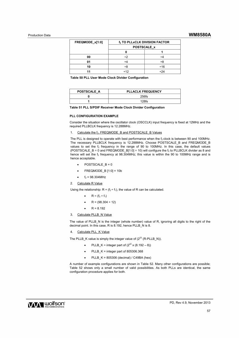
Production Data WM8580A
w PD, Rev 4.9, November 2013
57
FREQMODE_x[1:0] f2 TO PLLxCLK DIVISION FACTOR
POSTSCALE_x
0 1
00 ÷2 ÷4
01 ÷4 ÷8
10 ÷8 ÷16
11 ÷12 ÷24
Table 50 PLL User Mode Clock Divider Configuration
POSTSCALE_A PLLACLK FREQUENCY
0 256fs
1 128fs
Table 51 PLL S/PDIF Receiver Mode Clock Divider Configuration
PLL CONFIGURATION EXAMPLE
Consider the situation where the oscillator clock (OSCCLK) input frequency is fixed at 12MHz and the required PLLBCLK frequency is 12.288MHz.
1. Calculate the f2, FREQMODE_B and POSTSCALE_B Values
The PLL is designed to operate with best performance when the f2 clock is between 90 and 100MHz. The necessary PLLBCLK frequency is 12.288MHz. Choose POSTSCALE_B and FREQMODE_B values to set the f2 frequency in the range of 90 to 100MHz. In this case, the default values (POSTSCALE_B = 0 and FREQMODE_B[1:0] = 10) will configure the f2 to PLLBCLK divider as 8 and hence will set the f2 frequency at 98.304MHz; this value is within the 90 to 100MHz range and is hence acceptable.
POSTSCALE_B = 0
FREQMODE_B [1:0] = 10b
f2 = 98.304MHz
2. Calculate R Value
Using the relationship: R = (f2 ÷ f1), the value of R can be calculated.
R = (f2 ÷ f1)
R = (98.304 ÷ 12)
R = 8.192
3. Calculate PLLB_N Value
The value of PLLB_N is the integer (whole number) value of R, ignoring all digits to the right of the decimal point. In this case, R is 8.192, hence PLLB_N is 8.
4. Calculate PLL_K Value
The PLLB_K value is simply the integer value of (222 (R-PLLB_N)).
PLLB_K = integer part of (222 x (8.192 – 8))
PLLB_K = integer part of 805306.368
PLLB_K = 805306 (decimal) / C49BA (hex)
A number of example configurations are shown in Table 52. Many other configurations are possible; Table 52 shows only a small number of valid possibilities. As both PLLs are identical, the same configuration procedure applies for both.
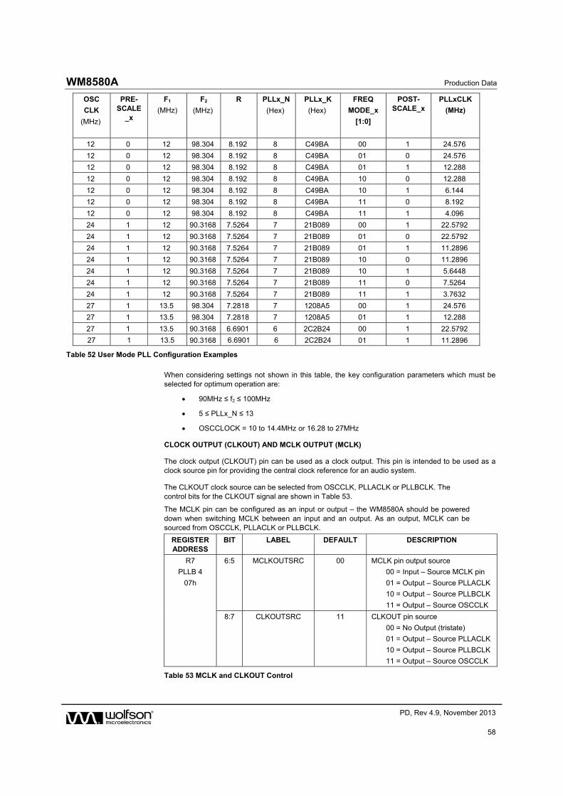
WM8580A Production Data
w PD, Rev 4.9, November 2013
58
OSC
CLK
(MHz)
PRE-SCALE
_x
F1
(MHz)
F2
(MHz)
R PLLx_N
(Hex)
PLLx_K
(Hex)
FREQ
MODE_x
[1:0]
POST-SCALE_x
PLLxCLK
(MHz)
12 0 12 98.304 8.192 8 C49BA 00 1 24.576
12 0 12 98.304 8.192 8 C49BA 01 0 24.576
12 0 12 98.304 8.192 8 C49BA 01 1 12.288
12 0 12 98.304 8.192 8 C49BA 10 0 12.288
12 0 12 98.304 8.192 8 C49BA 10 1 6.144
12 0 12 98.304 8.192 8 C49BA 11 0 8.192
12 0 12 98.304 8.192 8 C49BA 11 1 4.096
24 1 12 90.3168 7.5264 7 21B089 00 1 22.5792
24 1 12 90.3168 7.5264 7 21B089 01 0 22.5792
24 1 12 90.3168 7.5264 7 21B089 01 1 11.2896
24 1 12 90.3168 7.5264 7 21B089 10 0 11.2896
24 1 12 90.3168 7.5264 7 21B089 10 1 5.6448
24 1 12 90.3168 7.5264 7 21B089 11 0 7.5264
24 1 12 90.3168 7.5264 7 21B089 11 1 3.7632
27 1 13.5 98.304 7.2818 7 1208A5 00 1 24.576
27 1 13.5 98.304 7.2818 7 1208A5 01 1 12.288
27 1 13.5 90.3168 6.6901 6 2C2B24 00 1 22.5792
27 1 13.5 90.3168 6.6901 6 2C2B24 01 1 11.2896
Table 52 User Mode PLL Configuration Examples
When considering settings not shown in this table, the key configuration parameters which must be selected for optimum operation are:
90MHz ≤ f2 ≤ 100MHz
5 ≤ PLLx_N ≤ 13
OSCCLOCK = 10 to 14.4MHz or 16.28 to 27MHz
CLOCK OUTPUT (CLKOUT) AND MCLK OUTPUT (MCLK)
The clock output (CLKOUT) pin can be used as a clock output. This pin is intended to be used as a clock source pin for providing the central clock reference for an audio system.
The CLKOUT clock source can be selected from OSCCLK, PLLACLK or PLLBCLK. The control bits for the CLKOUT signal are shown in Table 53.
The MCLK pin can be configured as an input or output – the WM8580A should be powered down when switching MCLK between an input and an output. As an output, MCLK can be sourced from OSCCLK, PLLACLK or PLLBCLK.
REGISTER ADDRESS
BIT LABEL DEFAULT DESCRIPTION
R7
PLLB 4
07h
6:5 MCLKOUTSRC 00 MCLK pin output source
00 = Input – Source MCLK pin
01 = Output – Source PLLACLK
10 = Output – Source PLLBCLK
11 = Output – Source OSCCLK
8:7 CLKOUTSRC 11 CLKOUT pin source
00 = No Output (tristate)
01 = Output – Source PLLACLK
10 = Output – Source PLLBCLK
11 = Output – Source OSCCLK
Table 53 MCLK and CLKOUT Control
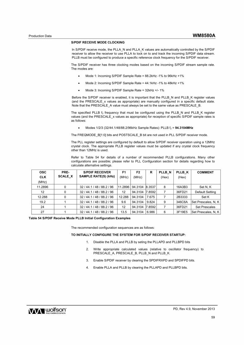
Production Data WM8580A
w PD, Rev 4.9, November 2013
59
S/PDIF RECEIVE MODE CLOCKING
In S/PDIF receive mode, the PLLA_N and PLLA_K values are automatically controlled by the S/PDIF receiver to allow the receiver to use PLLA to lock on to and track the incoming S/PDIF data stream. PLLB must be configured to produce a specific reference clock frequency for the S/PDIF receiver.
The S/PDIF receiver has three clocking modes based on the incoming S/PDIF stream sample rate. The modes are:
Mode 1: Incoming S/PDIF Sample Rate = 88.2kHz -1% to 96kHz +1%
Mode 2: Incoming S/PDIF Sample Rate = 44.1kHz -1% to 48kHz +1%
Mode 3: Incoming S/PDIF Sample Rate = 32kHz +/- 1%
Before the S/PDIF receiver is enabled, it is important that the PLLB_N and PLLB_K register values (and the PRESCALE_x values as appropriate) are manually configured in a specific default state. Note that the PRESCALE_A value must always be set to the same value as PRESCALE_B.
The specified PLLB f2 frequency that must be configured using the PLLB_N and PLLB_K register values (and the PRESCALE_x values as appropriate) for reception of specific S/PDIF sample rates is as follows:
Modes 1/2/3 (32/44.1/48/88.2/96kHz Sample Rates): PLLB f2 = 94.3104MHz
The FREQMODE_B[1:0] bits and POSTSCALE_B bit are not used in PLL S/PDIF receiver mode.
The PLL register settings are configured by default to allow S/PDIF receiver operation using a 12MHz crystal clock. The appropriate PLLB register values must be updated if any crystal clock frequency other than 12MHz is used.
Refer to Table 54 for details of a number of recommended PLLB configurations. Many other configurations are possible; please refer to PLL Configuration section for details regarding how to calculate alternative settings.
OSC
CLK
(MHz)
PRE-SCALE_X
S/PDIF RECEIVER SAMPLE RATE(S) (kHz)
F1
(MHz)
F2
(MHz)
R PLLB_N
(Hex)
PLLB_K
(Hex)
COMMENT
11.2896 0 32 / 44.1 / 48 / 88.2 / 96 11.2896 94.3104 8.3537 8 16A3B3 Set N, K
12 0 32 / 44.1 / 48 / 88.2 / 96 12 94.3104 7.8592 7 36FD21 Default Setting
12.288 0 32 / 44.1 / 48 / 88.2 / 96 12.288 94.3104 7.675 7 2B3333 Set K
19.2 1 32 / 44.1 / 48 / 88.2 / 96 9.6 94.3104 9.824 9 346C6A Set Prescales, N, K
24 1 32 / 44.1 / 48 / 88.2 / 96 12 94.3104 7.8592 7 36FD21 Set Prescales
27 1 32 / 44.1 / 48 / 88.2 / 96 13.5 94.3104 6.986 6 3F19E5 Set Prescales, N, K
Table 54 S/PDIF Receive Mode PLLB Initial Configuration Examples
The recommended configuration sequences are as follows:
TO INITIALLY CONFIGURE THE SYSTEM FOR S/PDIF RECEIVER STARTUP:
1. Disable the PLLA and PLLB by seting the PLLAPD and PLLBPD bits
2. Write appropriate calculated values (relative to oscillator frequency) to PRESCALE_A, PRESCALE_B, PLLB_N and PLLB_K.
3. Enable S/PDIF receiver by clearing the SPDIFRXPD and SPDIFPD bits.
4. Enable PLLA and PLLB by clearing the PLLAPD and PLLBPD bits.
WM8580A Production Data
w PD, Rev 4.9, November 2013
60
PHASE-LOCKED LOOPS AND S/PDIF CLOCKING (HARDWARE MODE)
In hardware mode, the user has no access to the internal clocking control registers and hence a default configuration is loaded at reset to provide maximum functionality.
The S/PDIF receiver is enabled and hence the PLLs operate in S/PDIF receiver mode and all PLL and S/PDIF receiver control is fully automatic. All supported S/PDIF receiver sample rates can be used.
FREQMODE_x and POSTSCALE_x control is fully automatic to ensure that the internal MCLK is maintained at 256fs relative to the S/PDIF received sample rate. In hardware mode, the internal MCLK is not available at the MCLK pin (the pin defaults to an input)
In hardware mode, the OSCCLK must be 12MHz and hence the external crystal (or applied XIN clock) must be 12MHz. No other OSCCLK frequencies are supported in hardware mode.
S/PDIF TRANSCEIVER
FEATURES
IEC-60958-3 compatible with 32k frames/s to 96k frames/s support
Support for Reception and Transmission of S/PDIF data
Clock synthesis PLL with reference clock input and ultra-low jitter output
Input mux with support for up to four S/PDIF inputs
Register controlled Channel Status recovery and transmission
Register read-back of recovered Channel Status bits and error flags
Detection of non-audio data, sample rate, and pre-emphasised data
Programmable GPO for error flags, frame status flags and clocks
An IEC-60958-3 compatible S/PDIF transceiver is integrated into the WM8580A. Operation of the S/PDIF function may be synchronous or asynchronous to the rest of the digital audio circuits.
The receiver performs data and clock recovery, and sends recovered data either to an external device such as a DSP (via the Digital Audio Interfaces), or if the data is audio PCM, it can route the stereo recovered data to DAC1. The recovered clock may be routed out of the WM8580A onto a pin for external use, and may be used to clock the internal DAC as required.
The transmitter generates S/PDIF frames where audio data may be sourced from the ADC, S/PDIF Receiver, or the Digital Audio Interfaces.
S/PDIF FORMAT
S/PDIF is a serial, bi-phase-mark encoded data stream. An S/PDIF frame consists of two sub-frames. Each sub-frame is made up of:
Preamble – a synchronization pattern used to identify the start of a 192-frame block or sub-frame
4-bit Auxiliary Data (AUX) – ordered LSB to MSB
20-bit Audio Data (24-bit when combined with AUX) – ordered LSB to MSB
Validity Bit – a 1 indicates invalid data in that sub-frame
User Bit – over 192-frames, this forms a User Data Block,
Channel Bit – over 192-frames, this forms a Channel Status Block
Parity Bit – used to maintain even parity over the sub-frame (except the preamble)
An S/PDIF Block consists of 192 frames. Channel and User blocks are incorporated within the 192-frame S/PDIF Block. For Consumer mode only the first 40-frames are used to make up the Channel and User blocks. Figure 39 illustrates the S/PDIF format.
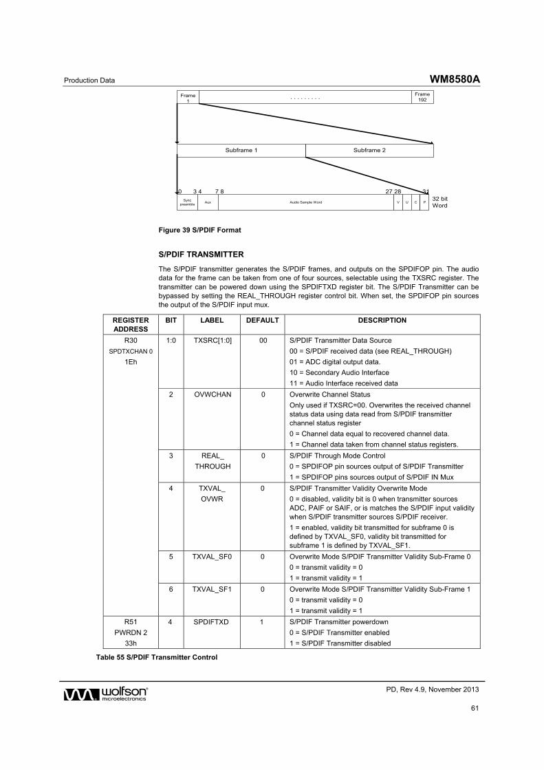
Production Data WM8580A
w PD, Rev 4.9, November 2013
61
. . . . . . . . . Frame192
Frame1
Subframe 1 Subframe 2
Syncpreamble
Aux V U C PAudio Sample Word
3 4 7 8 27 280 3132 bitWord
Figure 39 S/PDIF Format
S/PDIF TRANSMITTER
The S/PDIF transmitter generates the S/PDIF frames, and outputs on the SPDIFOP pin. The audio data for the frame can be taken from one of four sources, selectable using the TXSRC register. The transmitter can be powered down using the SPDIFTXD register bit. The S/PDIF Transmitter can be bypassed by setting the REAL_THROUGH register control bit. When set, the SPDIFOP pin sources the output of the S/PDIF input mux.
REGISTER ADDRESS
BIT LABEL DEFAULT DESCRIPTION
R30
SPDTXCHAN 0
1Eh
1:0 TXSRC[1:0] 00 S/PDIF Transmitter Data Source
00 = S/PDIF received data (see REAL_THROUGH)
01 = ADC digital output data.
10 = Secondary Audio Interface
11 = Audio Interface received data
2 OVWCHAN 0 Overwrite Channel Status
Only used if TXSRC=00. Overwrites the received channel status data using data read from S/PDIF transmitter channel status register
0 = Channel data equal to recovered channel data.
1 = Channel data taken from channel status registers.
3 REAL_
THROUGH
0 S/PDIF Through Mode Control
0 = SPDIFOP pin sources output of S/PDIF Transmitter
1 = SPDIFOP pins sources output of S/PDIF IN Mux
4 TXVAL_
OVWR
0 S/PDIF Transmitter Validity Overwrite Mode
0 = disabled, validity bit is 0 when transmitter sources ADC, PAIF or SAIF, or is matches the S/PDIF input validity when S/PDIF transmitter sources S/PDIF receiver.
1 = enabled, validity bit transmitted for subframe 0 is defined by TXVAL_SF0, validity bit transmitted for subframe 1 is defined by TXVAL_SF1.
5 TXVAL_SF0 0 Overwrite Mode S/PDIF Transmitter Validity Sub-Frame 0
0 = transmit validity = 0
1 = transmit validity = 1
6 TXVAL_SF1 0 Overwrite Mode S/PDIF Transmitter Validity Sub-Frame 1
0 = transmit validity = 0
1 = transmit validity = 1
R51
PWRDN 2
33h
4 SPDIFTXD 1 S/PDIF Transmitter powerdown
0 = S/PDIF Transmitter enabled
1 = S/PDIF Transmitter disabled
Table 55 S/PDIF Transmitter Control
WM8580A Production Data
w PD, Rev 4.9, November 2013
62
The WM8580A also transmits the preamble and VUCP bits (Validity, User Data, Channel Status and Parity bits).
Validity Bit
By default, set to 0 (to indicate valid data) with the following exceptions:
1. TXSRC=00 (S/PDIF receiver), where Validity is the value recovered from the S/PDIF input stream by the S/PDIF receiver.
2. TXVAL_OVWR=1, where Validity is the value set in registers TXVAL_SF0 and TXVAL_SF1.
User Data
Set to 0 as User Data configuration is not supported in the WM8580A – if TXSRC=00 (S/PDIF receiver) User Data is the value recovered from the S/PDIF input stream by the S/PDIF receiver.
Channel Status
The Channel Status bits form a 192 frame –lock - transmitted at one bit per sub-frame. Each sub-frame forms its own 192-frame block. The WM8580A is a consumer mode device and only the first 40 bits of the block are used. All data transmitted from the WM8580A is stereo, so the channel status data is duplicated for both channels. The only exception to this is the channel number bits (23:20) which can be changed to indicate whether the channel is left or right in the stereo image. Bits within this block can be configured by setting the Channel Status Bit Control registers (see Table 56 to Table 60). If TXSRC=00 (S/PDIF receiver), the Channel Status bits are transmitted with the same values recovered by the receiver – unless OVWCHAN is set, in which case they are set by the S/PDIF transmitter channel status registers.
Parity Bit
This bit maintains even parity for data as a means of basic error detection. It is generated by the transmitter.
For further details of all channel status bits, refer to IEC-60958-3.
REGISTER ADDRESS
BIT LABEL CHANNEL STATUS
BIT
DEFAULT DESCRIPTION
R31
SPDTXCHAN 1
1Fh
0 CON/PRO 0 0 0 = Consumer Mode
1 = Professional Mode (not supported by WM8580A)
1 AUDIO_N 1 0 Linear PCM Identification
0 = S/PDIF transmitted data is audio PCM.
1 = S/PDIF transmitted data is not audio PCM.
2 CPY_N 2 0 0 = Transmitted data has copyright asserted.
1 = Transmitted data has no copyright assertion.
5:3 DEEMPH[2:0] 5:3 000 000 = Data from Audio interface has no pre-emphasis.
001 = Data from Audio interface has pre-emphasis.
010 = Reserved (Audio interface has pre-emphasis).
011 = Reserved (Audio interface has pre-emphasis).
All other modes are reserved and should not be used.
7:6 CHSTMODE
[1:0]
7:6 00 00 = Only valid mode for consumer applications.
Table 56 S/PDIF Transmitter Channel Status Bit Control 1
Production Data WM8580A
w PD, Rev 4.9, November 2013
63
REGISTER ADDRESS
BIT LABEL CHANNEL STATUS
BIT
DEFAULT DESCRIPTION
R32
SPDTXCHAN 2
20h
7:0 CATCODE
[7:0]
15:8 00000000 Category Code. Refer to S/PDIF specification IEC60958-3 for details.
00h indicates “general” mode.
Table 57 S/PDIF Transmitter Channel Status Bit Control 2
REGISTER ADDRESS
BIT LABEL CHANNEL STATUS
BIT
DEFAULT DESCRIPTION
R33
SPDTXCHAN 3
21h
3:0 SRCNUM
[3:0]
19:16 0000 Indicates S/PDIF source number.
No definitions are attached to data.
5:4 CHNUM1[1:0] 21:20
23:22
00 Channel Number for Subframe 1
CHNUM1 Function
00 Do not use channel number
01 Send to Left Channel
10 Send to Right Channel
11 Do not use channel number
7:6 CHNUM2[1:0] 00 Channel Number for Subframe 2
CHNUM2 Function
00 Do not use channel number
01 Send to Left Channel
10 Send to Right Channel
11 Do not use channel number
Table 58 S/PDIF Transmitter Channel Status Bit Control 3
REGISTER ADDRESS
BIT LABEL CHANNEL STATUS
BIT
DEFAULT DESCRIPTION
R34
SPDTXCHAN 4
22h
3:0 FREQ[3:0] 27:24 0001 Sampling Frequency Indicated
See S/PDIF specification IEC60958-3 for details.
0001 = Sampling Frequency not indicated.
5:4 CLKACU[1:0] 29:28 11 Clock Accuracy of Transmitted clock.
00 = Level II
01 = Level I
10 = Level III
11 = Interface frame rate not matched to sampling frequency.
Table 59 S/PDIF Transmitter Channel Status Bit Control 4
WM8580A Production Data
w PD, Rev 4.9, November 2013
64
REGISTER ADDRESS
BIT LABEL CHANNEL STATUS BIT
DEFAULT DESCRIPTION
R35
SPDTXCHAN 5
23h
0 MAXWL 32 1 Maximum Audio sample word length
0 = 20 bits
1 = 24 bits
3:1 TXWL[2:0] 35:33 101 Audio Sample Word Length.
000 = Word Length Not Indicated
TXWL[2:0] MAXWL==1 MAXWL==0
001 20 bits 16 bits
010 22 bits 18 bits
100 23 bits 19 bits
101 24 bits 20 bits
110 21 bits 17 bits
All other combinations reserved
7:4 ORGSAMP
[3:0]
39:36 0000 Original Sampling Frequency. See S/PDIF specification for details.
0000 = original sampling frequency not indicated
Table 60 S/PDIF Transmitter Channel Status Bit Control 5
S/PDIF RECEIVER
INPUT SELECTOR
The S/PDIF receiver has one dedicated input, SPDIFIN1. This pin is a IEC-60958-3-compatible comparator input by default or, if SPDIFIN1MODE is set, the pin will be a CMOS-compatible input. There are three other pins which can be configured as either S/PDIF inputs or general purpose outputs (GPOs). The four S/PDIF inputs are multiplexed to allow one input to go to the S/PDIF receiver for decoding. The S/PDIF receiver can be powered down using the SPDIFRXD register bit.
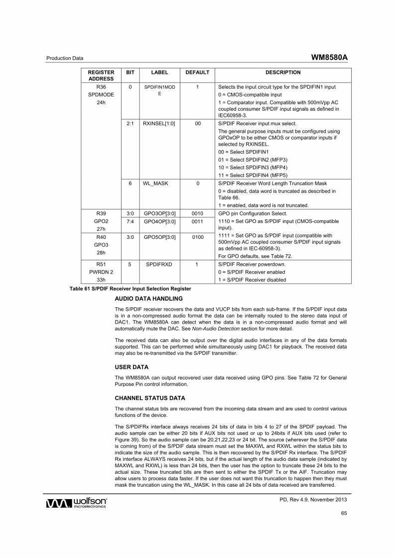
Production Data WM8580A
w PD, Rev 4.9, November 2013
65
Table 61 S/PDIF Receiver Input Selection Register
AUDIO DATA HANDLING
The S/PDIF receiver recovers the data and VUCP bits from each sub-frame. If the S/PDIF input data is in a non-compressed audio format the data can be internally routed to the stereo data input of DAC1. The WM8580A can detect when the data is in a non-compressed audio format and will automatically mute the DAC. See Non-Audio Detection section for more detail.
The received data can also be output over the digital audio interfaces in any of the data formats supported. This can be performed while simultaneously using DAC1 for playback. The received data may also be re-transmitted via the S/PDIF transmitter.
USER DATA
The WM8580A can output recovered user data received using GPO pins. See Table 72 for General Purpose Pin control information.
CHANNEL STATUS DATA
The channel status bits are recovered from the incoming data stream and are used to control various functions of the device.
The S/PDIFRx interface always receives 24 bits of data in bits 4 to 27 of the SPDIF payload. The audio sample can be either 20 bits if AUX bits not used or up to 24bits if AUX bits used (refer to Figure 39). So the audio sample can be 20,21,22,23 or 24 bit. The source (wherever the S/PDIF data is coming from) of the S/PDIF data stream must set the MAXWL and RXWL within the status bits to indicate the size of the audio sample. This is then recovered by the S/PDIF Rx interface. The S/PDIF Rx interface ALWAYS receives 24 bits, but if the actual length of the audio data sample (indicated by MAXWL and RXWL) is less than 24 bits, then the user has the option to truncate these 24 bits to the actual size. These truncated bits are then sent to either the SPDIF Tx or the AIF. Truncation may allow users to process data faster. If the user does not want this truncation to happen then they must mask the truncation using the WL_MASK. In this case all 24 bits of data received are transferred.
REGISTER ADDRESS
BIT LABEL DEFAULT DESCRIPTION
R36
SPDMODE
24h
0 SPDIFIN1MOD
E 1 Selects the input circuit type for the SPDIFIN1 input
0 = CMOS-compatible input
1 = Comparator input. Compatible with 500mVpp AC coupled consumer S/PDIF input signals as defined in IEC60958-3.
2:1 RXINSEL[1:0] 00 S/PDIF Receiver input mux select.
The general purpose inputs must be configured using GPOxOP to be either CMOS or comparator inputs if selected by RXINSEL.
00 = Select SPDIFIN1
01 = Select SPDIFIN2 (MFP3)
10 = Select SPDIFIN3 (MFP4)
11 = Select SPDIFIN4 (MFP5)
6 WL_MASK 0 S/PDIF Receiver Word Length Truncation Mask
0 = disabled, data word is truncated as described in Table 66.
1 = enabled, data word is not truncated.
R39
GPO2
27h
3:0 GPO3OP[3:0] 0010 GPO pin Configuration Select.
1110 = Set GPO as S/PDIF input (CMOS-compatible input).
1111 = Set GPO as S/PDIF input (compatible with 500mVpp AC coupled consumer S/PDIF input signals as defined in IEC-60958-3).
For GPO defaults, see Table 72.
7:4 GPO4OP[3:0] 0011
R40
GPO3
28h
3:0 GPO5OP[3:0] 0100
R51
PWRDN 2
33h
5 SPDIFRXD 1 S/PDIF Receiver powerdown.
0 = S/PDIF Receiver enabled
1 = S/PDIF Receiver disabled
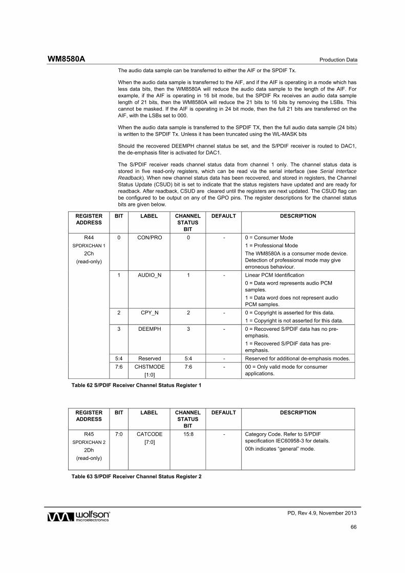
WM8580A Production Data
w PD, Rev 4.9, November 2013
66
The audio data sample can be transferred to either the AIF or the SPDIF Tx.
When the audio data sample is transferred to the AIF, and if the AIF is operating in a mode which has less data bits, then the WM8580A will reduce the audio data sample to the length of the AIF. For example, if the AIF is operating in 16 bit mode, but the SPDIF Rx receives an audio data sample length of 21 bits, then the WM8580A will reduce the 21 bits to 16 bits by removing the LSBs. This cannot be masked. If the AIF is operating in 24 bit mode, then the full 21 bits are transferred on the AIF, with the LSBs set to 000.
When the audio data sample is transferred to the SPDIF TX, then the full audio data sample (24 bits) is written to the SPDIF Tx. Unless it has been truncated using the WL-MASK bits
Should the recovered DEEMPH channel status be set, and the S/PDIF receiver is routed to DAC1, the de-emphasis filter is activated for DAC1.
The S/PDIF receiver reads channel status data from channel 1 only. The channel status data is stored in five read-only registers, which can be read via the serial interface (see Serial Interface Readback). When new channel status data has been recovered, and stored in registers, the Channel Status Update (CSUD) bit is set to indicate that the status registers have updated and are ready for readback. After readback, CSUD are cleared until the registers are next updated. The CSUD flag can be configured to be output on any of the GPO pins. The register descriptions for the channel status bits are given below.
REGISTER ADDRESS
BIT LABEL CHANNEL STATUS
BIT
DEFAULT DESCRIPTION
R44
SPDRXCHAN 1
2Ch
(read-only)
0 CON/PRO 0 - 0 = Consumer Mode
1 = Professional Mode
The WM8580A is a consumer mode device. Detection of professional mode may give erroneous behaviour.
1 AUDIO_N 1 - Linear PCM Identification
0 = Data word represents audio PCM samples.
1 = Data word does not represent audio PCM samples.
2 CPY_N 2 - 0 = Copyright is asserted for this data.
1 = Copyright is not asserted for this data.
3 DEEMPH 3 - 0 = Recovered S/PDIF data has no pre-emphasis.
1 = Recovered S/PDIF data has pre-emphasis.
5:4 Reserved 5:4 - Reserved for additional de-emphasis modes.
7:6 CHSTMODE
[1:0]
7:6 - 00 = Only valid mode for consumer applications.
Table 62 S/PDIF Receiver Channel Status Register 1
REGISTER ADDRESS
BIT LABEL CHANNEL STATUS
BIT
DEFAULT DESCRIPTION
R45
SPDRXCHAN 2
2Dh
(read-only)
7:0 CATCODE
[7:0]
15:8 - Category Code. Refer to S/PDIF specification IEC60958-3 for details.
00h indicates “general” mode.
Table 63 S/PDIF Receiver Channel Status Register 2
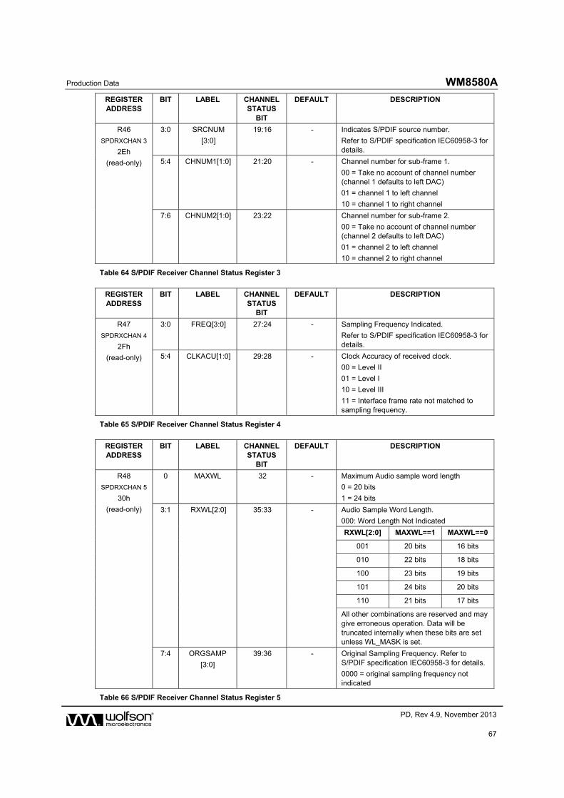
Production Data WM8580A
w PD, Rev 4.9, November 2013
67
REGISTER ADDRESS
BIT LABEL CHANNEL STATUS
BIT
DEFAULT DESCRIPTION
R46
SPDRXCHAN 3
2Eh
(read-only)
3:0 SRCNUM
[3:0]
19:16 - Indicates S/PDIF source number.
Refer to S/PDIF specification IEC60958-3 for details.
5:4 CHNUM1[1:0] 21:20 - Channel number for sub-frame 1.
00 = Take no account of channel number (channel 1 defaults to left DAC)
01 = channel 1 to left channel
10 = channel 1 to right channel
7:6 CHNUM2[1:0] 23:22 Channel number for sub-frame 2.
00 = Take no account of channel number (channel 2 defaults to left DAC)
01 = channel 2 to left channel
10 = channel 2 to right channel
Table 64 S/PDIF Receiver Channel Status Register 3
REGISTER ADDRESS
BIT LABEL CHANNEL STATUS
BIT
DEFAULT DESCRIPTION
R47
SPDRXCHAN 4
2Fh
(read-only)
3:0 FREQ[3:0] 27:24 - Sampling Frequency Indicated.
Refer to S/PDIF specification IEC60958-3 for details.
5:4 CLKACU[1:0] 29:28 - Clock Accuracy of received clock.
00 = Level II
01 = Level I
10 = Level III
11 = Interface frame rate not matched to sampling frequency.
Table 65 S/PDIF Receiver Channel Status Register 4
REGISTER ADDRESS
BIT LABEL CHANNEL STATUS
BIT
DEFAULT DESCRIPTION
R48
SPDRXCHAN 5
30h
(read-only)
0 MAXWL 32 - Maximum Audio sample word length
0 = 20 bits
1 = 24 bits
3:1 RXWL[2:0] 35:33 - Audio Sample Word Length.
000: Word Length Not Indicated
RXWL[2:0] MAXWL==1 MAXWL==0
001 20 bits 16 bits
010 22 bits 18 bits
100 23 bits 19 bits
101 24 bits 20 bits
110 21 bits 17 bits
All other combinations are reserved and may give erroneous operation. Data will be truncated internally when these bits are set unless WL_MASK is set.
7:4 ORGSAMP
[3:0]
39:36 - Original Sampling Frequency. Refer to S/PDIF specification IEC60958-3 for details.
0000 = original sampling frequency not indicated
Table 66 S/PDIF Receiver Channel Status Register 5
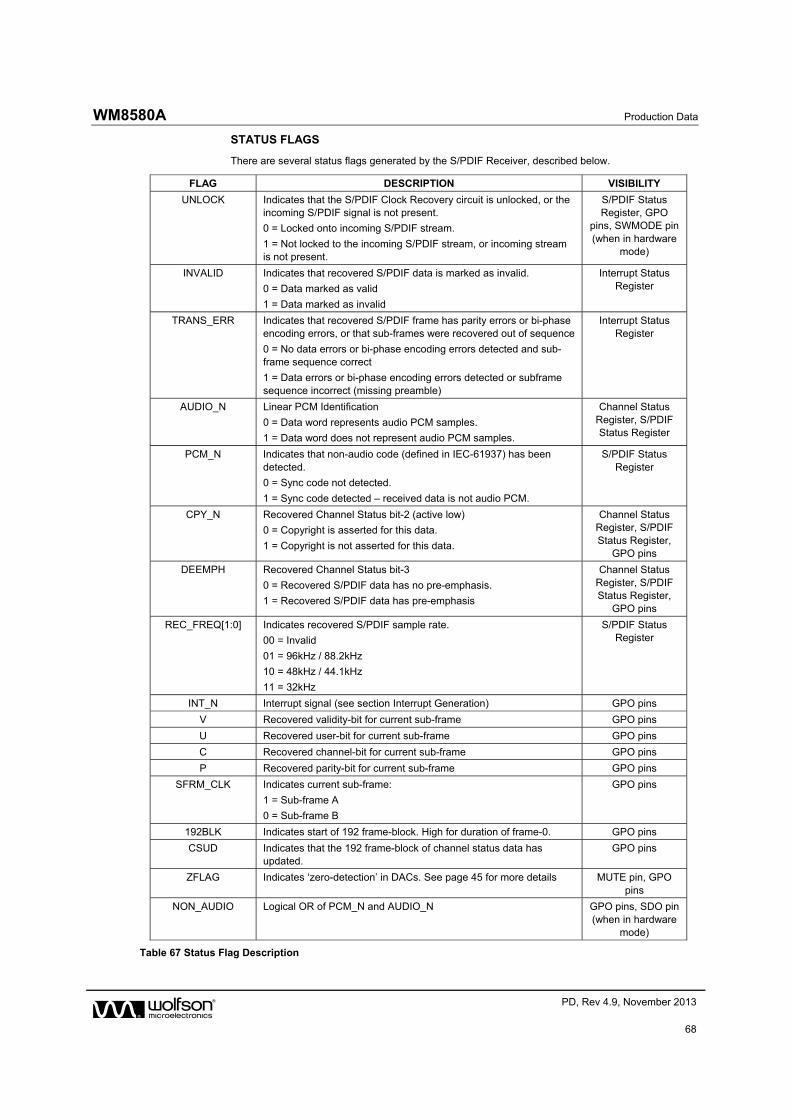
WM8580A Production Data
w PD, Rev 4.9, November 2013
68
STATUS FLAGS
There are several status flags generated by the S/PDIF Receiver, described below.
FLAG DESCRIPTION VISIBILITY
UNLOCK Indicates that the S/PDIF Clock Recovery circuit is unlocked, or the incoming S/PDIF signal is not present.
0 = Locked onto incoming S/PDIF stream.
1 = Not locked to the incoming S/PDIF stream, or incoming stream is not present.
S/PDIF Status Register, GPO
pins, SWMODE pin (when in hardware
mode)
INVALID Indicates that recovered S/PDIF data is marked as invalid.
0 = Data marked as valid
1 = Data marked as invalid
Interrupt Status Register
TRANS_ERR Indicates that recovered S/PDIF frame has parity errors or bi-phase encoding errors, or that sub-frames were recovered out of sequence
0 = No data errors or bi-phase encoding errors detected and sub-frame sequence correct
1 = Data errors or bi-phase encoding errors detected or subframe sequence incorrect (missing preamble)
Interrupt Status Register
AUDIO_N Linear PCM Identification
0 = Data word represents audio PCM samples.
1 = Data word does not represent audio PCM samples.
Channel Status Register, S/PDIF Status Register
PCM_N Indicates that non-audio code (defined in IEC-61937) has been detected.
0 = Sync code not detected.
1 = Sync code detected – received data is not audio PCM.
S/PDIF Status Register
CPY_N Recovered Channel Status bit-2 (active low)
0 = Copyright is asserted for this data.
1 = Copyright is not asserted for this data.
Channel Status Register, S/PDIF Status Register,
GPO pins
DEEMPH Recovered Channel Status bit-3
0 = Recovered S/PDIF data has no pre-emphasis.
1 = Recovered S/PDIF data has pre-emphasis
Channel Status Register, S/PDIF Status Register,
GPO pins
REC_FREQ[1:0] Indicates recovered S/PDIF sample rate.
00 = Invalid
01 = 96kHz / 88.2kHz
10 = 48kHz / 44.1kHz
11 = 32kHz
S/PDIF Status Register
INT_N Interrupt signal (see section Interrupt Generation) GPO pins
V Recovered validity-bit for current sub-frame GPO pins
U Recovered user-bit for current sub-frame GPO pins
C Recovered channel-bit for current sub-frame GPO pins
P Recovered parity-bit for current sub-frame GPO pins
SFRM_CLK Indicates current sub-frame:
1 = Sub-frame A
0 = Sub-frame B
GPO pins
192BLK Indicates start of 192 frame-block. High for duration of frame-0. GPO pins
CSUD Indicates that the 192 frame-block of channel status data has updated.
GPO pins
ZFLAG Indicates ‘zero-detection’ in DACs. See page 45 for more details MUTE pin, GPO pins
NON_AUDIO Logical OR of PCM_N and AUDIO_N GPO pins, SDO pin (when in hardware
mode)
Table 67 Status Flag Description
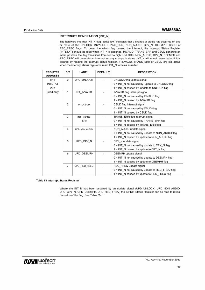
Production Data WM8580A
w PD, Rev 4.9, November 2013
69
INTERRUPT GENERATION (INT_N)
The hardware interrupt INT_N flag (active low) indicates that a change of status has occurred on one or more of the UNLOCK, INVALID, TRANS_ERR, NON_AUDIO, CPY_N, DEEMPH, CSUD or REC_FREQ flags. To determine which flag caused the interrupt, the Interrupt Status Register (INTSTAT) should be read when INT_N is asserted. INVALID, TRANS_ERR and CSUD generate an interrupt when the flag transitions from low to high. UNLOCK, NON_AUDIO, CPY_N, DEEMPH and REC_FREQ will generate an interrupt on any change in status. INT_N will remain asserted until it is cleared by reading the interrupt status register. If INVALID, TRANS_ERR or CSUD are still active when the interrupt status register is read, INT_N remains asserted.
Table 68 Interrupt Status Register
Where the INT_N has been asserted by an update signal (UPD_UNLOCK, UPD_NON_AUDIO, UPD_CPY_N, UPD_DEEMPH, UPD_REC_FREQ) the S/PDIF Status Register can be read to reveal the satus of the flag. See Table 69.
REGISTER ADDRESS
BIT LABEL DEFAULT DESCRIPTION
R43
INTSTAT
2Bh
(read-only)
0 UPD_UNLOCK - UNLOCK flag update signal
0 = INT_N not caused by update to UNLOCK flag
1 = INT_N caused by update to UNLOCK flag
1 INT_INVALID - INVALID flag interrupt signal
0 = INT_N not caused by INVALID flag
1 = INT_N caused by INVALID flag
2 INT_CSUD - CSUD flag interrupt signal
0 = INT_N not caused by CSUD flag
1 = INT_N caused by CSUD flag
3 INT_TRANS
_ERR
- TRANS_ERR flag interrupt signal
0 = INT_N not caused by TRANS_ERR flag
1 = INT_N caused by TRANS_ERR flag
4 UPD_NON_AUDIO - NON_AUDIO update signal
0 = INT_N not caused by update to NON_AUDIO flag
1 = INT_N caused by update to NON_AUDIO flag
5 UPD_CPY_N - CPY_N update signal
0 = INT_N not caused by update to CPY_N flag
1 = INT_N caused by update to CPY_N flag
6 UPD_DEEMPH - DEEMPH update signal
0 = INT_N not caused by update to DEEMPH flag
1 = INT_N caused by update to DEEMPH flag
7 UPD_REC_FREQ - REC_FREQ update signal
0 = INT_N not caused by update to REC_FREQ flag
1 = INT_N caused by update to REC_FREQ flag
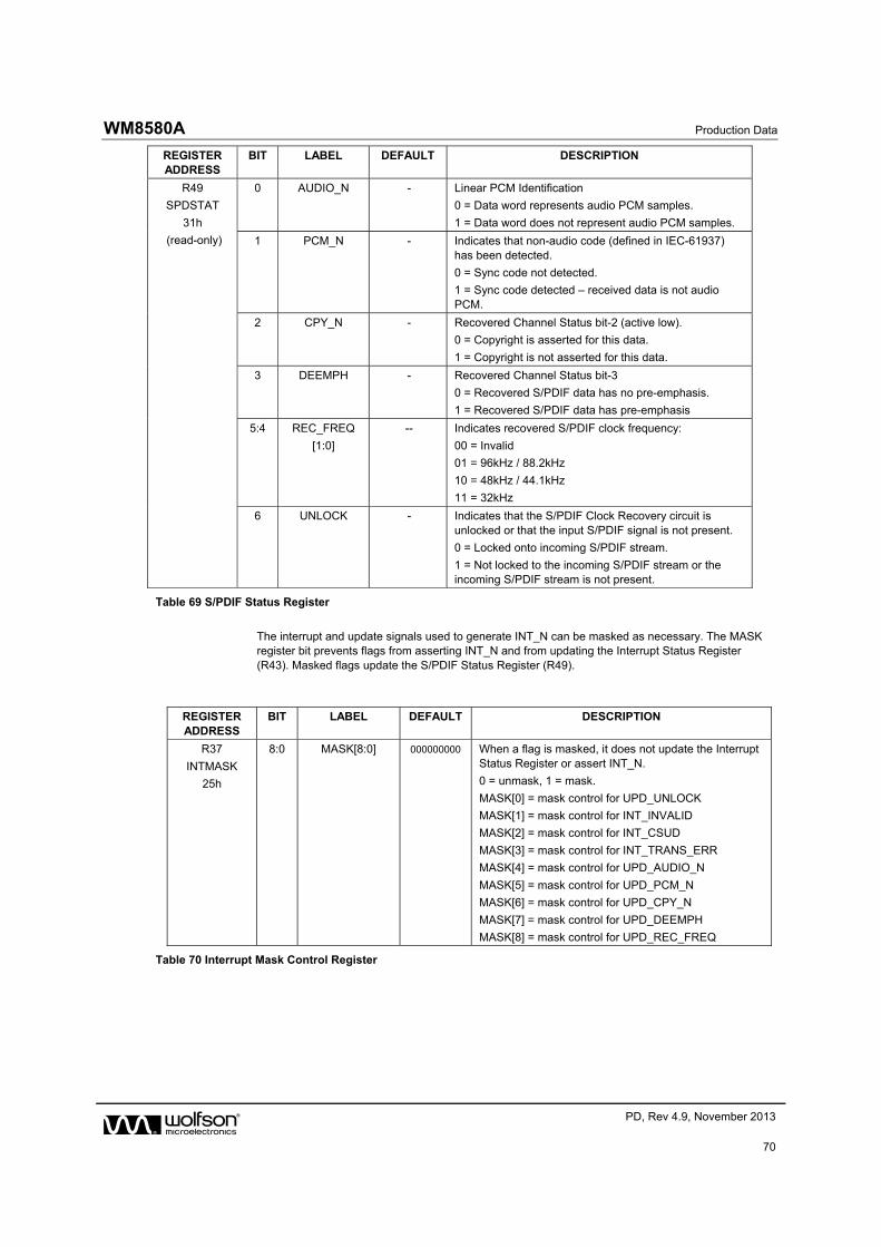
WM8580A Production Data
w PD, Rev 4.9, November 2013
70
REGISTER ADDRESS
BIT LABEL DEFAULT DESCRIPTION
R49
SPDSTAT
31h
(read-only)
0 AUDIO_N - Linear PCM Identification
0 = Data word represents audio PCM samples.
1 = Data word does not represent audio PCM samples.
1 PCM_N - Indicates that non-audio code (defined in IEC-61937) has been detected.
0 = Sync code not detected.
1 = Sync code detected – received data is not audio PCM.
2 CPY_N - Recovered Channel Status bit-2 (active low).
0 = Copyright is asserted for this data.
1 = Copyright is not asserted for this data.
3 DEEMPH - Recovered Channel Status bit-3
0 = Recovered S/PDIF data has no pre-emphasis.
1 = Recovered S/PDIF data has pre-emphasis
5:4 REC_FREQ
[1:0]
-- Indicates recovered S/PDIF clock frequency:
00 = Invalid
01 = 96kHz / 88.2kHz
10 = 48kHz / 44.1kHz
11 = 32kHz
6 UNLOCK - Indicates that the S/PDIF Clock Recovery circuit is unlocked or that the input S/PDIF signal is not present.
0 = Locked onto incoming S/PDIF stream.
1 = Not locked to the incoming S/PDIF stream or the incoming S/PDIF stream is not present.
Table 69 S/PDIF Status Register
The interrupt and update signals used to generate INT_N can be masked as necessary. The MASK register bit prevents flags from asserting INT_N and from updating the Interrupt Status Register (R43). Masked flags update the S/PDIF Status Register (R49).
REGISTER ADDRESS
BIT LABEL DEFAULT DESCRIPTION
R37
INTMASK
25h
8:0 MASK[8:0] 000000000 When a flag is masked, it does not update the Interrupt Status Register or assert INT_N.
0 = unmask, 1 = mask.
MASK[0] = mask control for UPD_UNLOCK
MASK[1] = mask control for INT_INVALID
MASK[2] = mask control for INT_CSUD
MASK[3] = mask control for INT_TRANS_ERR
MASK[4] = mask control for UPD_AUDIO_N
MASK[5] = mask control for UPD_PCM_N
MASK[6] = mask control for UPD_CPY_N
MASK[7] = mask control for UPD_DEEMPH
MASK[8] = mask control for UPD_REC_FREQ
Table 70 Interrupt Mask Control Register
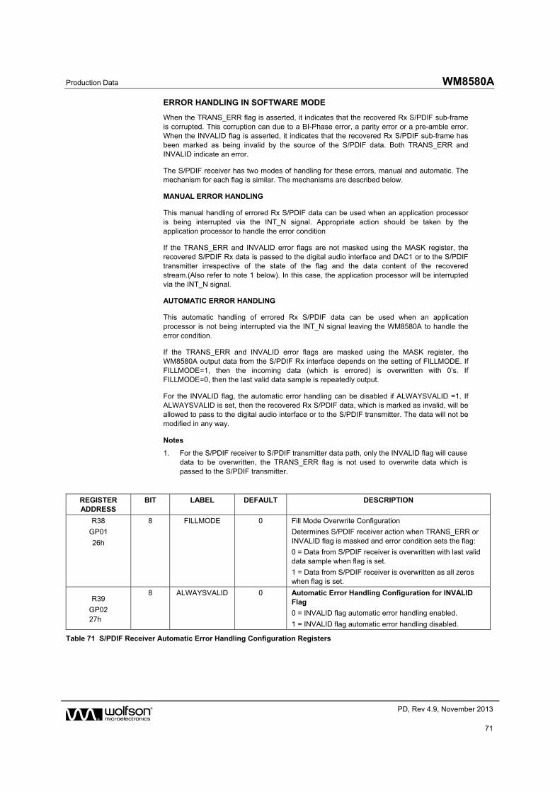
Production Data WM8580A
w PD, Rev 4.9, November 2013
71
ERROR HANDLING IN SOFTWARE MODE
When the TRANS_ERR flag is asserted, it indicates that the recovered Rx S/PDIF sub-frame is corrupted. This corruption can due to a BI-Phase error, a parity error or a pre-amble error. When the INVALID flag is asserted, it indicates that the recovered Rx S/PDIF sub-frame has been marked as being invalid by the source of the S/PDIF data. Both TRANS_ERR and INVALID indicate an error.
The S/PDIF receiver has two modes of handling for these errors, manual and automatic. The mechanism for each flag is similar. The mechanisms are described below.
MANUAL ERROR HANDLING
This manual handling of errored Rx S/PDIF data can be used when an application processor is being interrupted via the INT_N signal. Appropriate action should be taken by the application processor to handle the error condition
If the TRANS_ERR and INVALID error flags are not masked using the MASK register, the recovered S/PDIF Rx data is passed to the digital audio interface and DAC1 or to the S/PDIF transmitter irrespective of the state of the flag and the data content of the recovered stream.(Also refer to note 1 below). In this case, the application processor will be interrupted via the INT_N signal.
AUTOMATIC ERROR HANDLING
This automatic handling of errored Rx S/PDIF data can be used when an application processor is not being interrupted via the INT_N signal leaving the WM8580A to handle the error condition.
If the TRANS_ERR and INVALID error flags are masked using the MASK register, the WM8580A output data from the S/PDIF Rx interface depends on the setting of FILLMODE. If FILLMODE=1, then the incoming data (which is errored) is overwritten with 0’s. If FILLMODE=0, then the last valid data sample is repeatedly output.
For the INVALID flag, the automatic error handling can be disabled if ALWAYSVALID =1. If ALWAYSVALID is set, then the recovered Rx S/PDIF data, which is marked as invalid, will be allowed to pass to the digital audio interface or to the S/PDIF transmitter. The data will not be modified in any way.
Notes
1. For the S/PDIF receiver to S/PDIF transmitter data path, only the INVALID flag will cause data to be overwritten, the TRANS_ERR flag is not used to overwrite data which is passed to the S/PDIF transmitter.
REGISTER ADDRESS
BIT LABEL DEFAULT DESCRIPTION
R38
GP01
26h
8 FILLMODE 0 Fill Mode Overwrite Configuration
Determines S/PDIF receiver action when TRANS_ERR or INVALID flag is masked and error condition sets the flag:
0 = Data from S/PDIF receiver is overwritten with last valid data sample when flag is set.
1 = Data from S/PDIF receiver is overwritten as all zeros when flag is set.
R39
GP02 27h
8 ALWAYSVALID 0 Automatic Error Handling Configuration for INVALID Flag
0 = INVALID flag automatic error handling enabled.
1 = INVALID flag automatic error handling disabled.
Table 71 S/PDIF Receiver Automatic Error Handling Configuration Registers
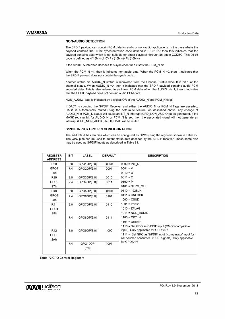
WM8580A Production Data
w PD, Rev 4.9, November 2013
72
NON-AUDIO DETECTION
The SPDIF payload can contain PCM data for audio or non-audio applications. In the case where the payload contains the 96 bit synchronization code defined in IEC61937 then this indicates that the payload contains data which is not suitable for direct playback through an audio CODEC. This 96 bit code is defined as 4*16bits of ‘0’+Pa (16bits)+Pb (16bits)..
If the SPDIFRx interface decodes this sync code then it sets the PCM_N bit.
When the PCM_N =1, then it indicates non-audio data. When the PCM_N =0, then it indicates that the SPDIF payload does not contain the synch code..
Another status bit, AUDIO_N status is recovered from the Channel Status block.It is bit 1 of the channel status. When AUDIO_N =0, then it indicates that the SPDIF payload contains audio PCM encoded data. This is also referred to as linear PCM data.When the AUDIO_N= 1, then it indicates that the SPDIF payload does not contain audio PCM data.
NON_AUDIO data is indicated by a logical OR of the AUDIO_N and PCM_N flags.
If DAC1 is sourcing the S/PDIF Receiver and either the AUDIO_N or PCM_N flags are asserted, DAC1 is automatically muted using the soft mute feature. As described above, any change of AUDIO_N or PCM_N status will cause an INT_N interrupt (UPD_NON_AUDIO) to be generated. If the MASK register bit for AUDIO_N or PCM_N is set, then the associated signal will not generate an interrupt (UPD_NON_AUDIO) but the DAC will be muted.
S/PDIF INPUT/ GPO PIN CONFIGURATION
The WM8580A has ten pins which can be configured as GPOs using the registers shown in Table 72. The GPO pins can be used to output status data decoded by the S/PDIF receiver. These same pins may be used as S/PDIF inputs as described in Table 61.
REGISTER ADDRESS
BIT LABEL DEFAULT DESCRIPTION
R38
GPO1
26h
3:0 GPO1OP[3:0] 0000 0000 = INT_N
0001 = V
0010 = U
0011 = C
0100 = P
0101 = SFRM_CLK
0110 = 192BLK
0111 = UNLOCK
1000 = CSUD
1001 = Invalid
1010 = ZFLAG
1011 = NON_AUDIO
1100 = CPY_N
1101 = DEEMP
1110 = Set GPO as S/PDIF input (CMOS-compatible input). Only applicable for GPO3/4/5.
1111 = Set GPO as S/PDIF input (‘comparator’ input for AC coupled consumer S/PDIF signals). Only applicable for GPO3/4/5
7:4 GPO2OP[3:0] 0001
R39
GPO2
27h
3:0 GPO3OP[3:0] 0010
7:4 GPO4OP[3:0] 0011
R40
GPO3
28h
3:0 GPO5OP[3:0] 0100
7:4 GPO6OP[3:0] 0101
R41
GPO4
29h
3:0 GPO7OP[3:0] 0110
7:4 GPO8OP[3:0] 0111
R42
GPO5
2Ah
3:0 GPO9OP[3:0] 1000
7:4 GPO10OP
[3:0]
1001
Table 72 GPO Control Registers
Production Data WM8580A
w PD, Rev 4.9, November 2013
73
POWERDOWN MODES
The WM8580A has powerdown control bits allowing specific parts of the chip to be turned off when not in use.
The ADC is powered down by setting the ADCPD register bit. The three stereo DACs each have a separate powerdown control bit, DACPD[2:0], allowing individual stereo DACs to be powered down when not in use. DACPD can be overwritten by setting ALLDACPD to powerdown all DACs
The S/PDIF transmitter is powered down by setting SPDIFTXD. Setting SPDIFRXD powers down the S/PDIF receiver.
The PLL, Oscillator and S/PDIF clock recovery circuits are powered down by setting PLLPD, OSCPD and SPDIFPD respectively.
Setting all of ADCPD, DACPD[2:0], SPDIFTXD, SPDIFRXD and OUTPD[3:0] will powerdown everything except the references VMIDADC, ADCREF and VMIDDAC. These may be powered down by setting PWDN. Setting PWDN will override all other powerdown control bits. It is recommended that the ADC and DAC are powered down before setting PWDN. The default is for all powerdown bits to be set except OSCPD and PWDN.
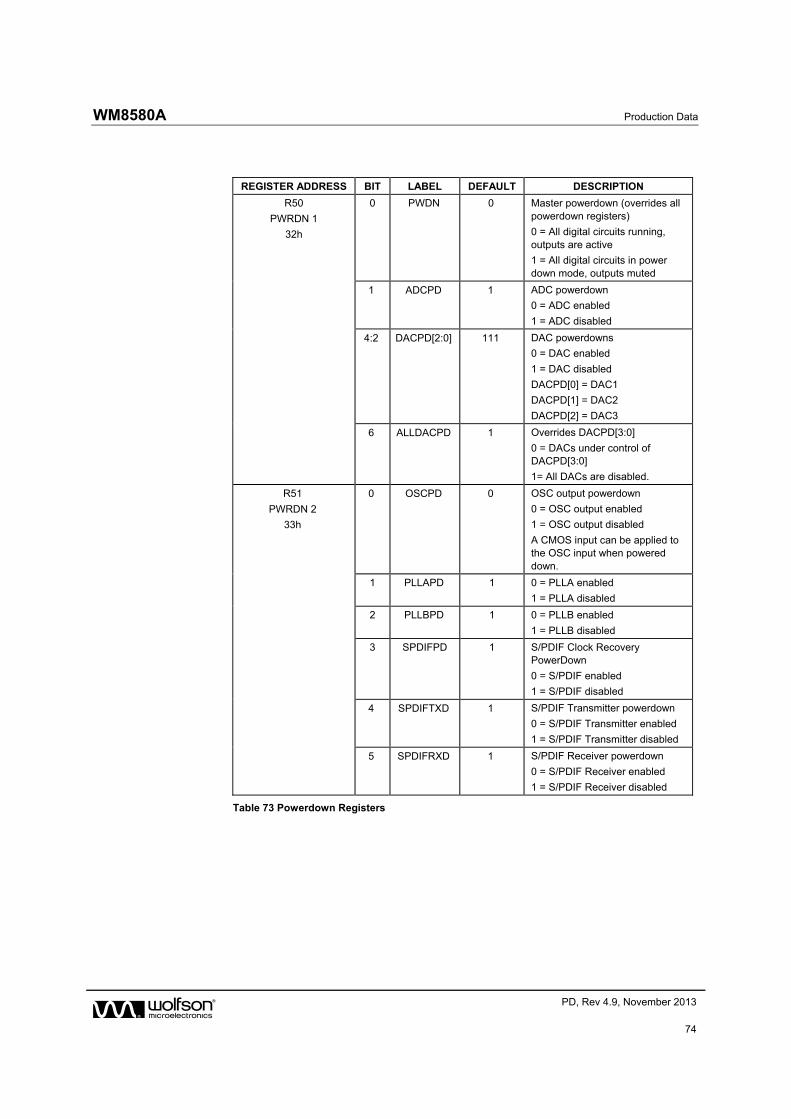
WM8580A Production Data
w PD, Rev 4.9, November 2013
74
REGISTER ADDRESS BIT LABEL DEFAULT DESCRIPTION
R50
PWRDN 1
32h
0 PWDN 0 Master powerdown (overrides all powerdown registers)
0 = All digital circuits running, outputs are active
1 = All digital circuits in power down mode, outputs muted
1 ADCPD 1 ADC powerdown
0 = ADC enabled
1 = ADC disabled
4:2 DACPD[2:0] 111 DAC powerdowns
0 = DAC enabled
1 = DAC disabled
DACPD[0] = DAC1
DACPD[1] = DAC2
DACPD[2] = DAC3
6 ALLDACPD 1 Overrides DACPD[3:0]
0 = DACs under control of DACPD[3:0]
1= All DACs are disabled.
R51
PWRDN 2
33h
0 OSCPD 0 OSC output powerdown
0 = OSC output enabled
1 = OSC output disabled
A CMOS input can be applied to the OSC input when powered down.
1 PLLAPD 1 0 = PLLA enabled
1 = PLLA disabled
2 PLLBPD 1 0 = PLLB enabled
1 = PLLB disabled
3 SPDIFPD 1 S/PDIF Clock Recovery PowerDown
0 = S/PDIF enabled
1 = S/PDIF disabled
4 SPDIFTXD 1 S/PDIF Transmitter powerdown
0 = S/PDIF Transmitter enabled
1 = S/PDIF Transmitter disabled
5 SPDIFRXD 1 S/PDIF Receiver powerdown
0 = S/PDIF Receiver enabled
1 = S/PDIF Receiver disabled
Table 73 Powerdown Registers
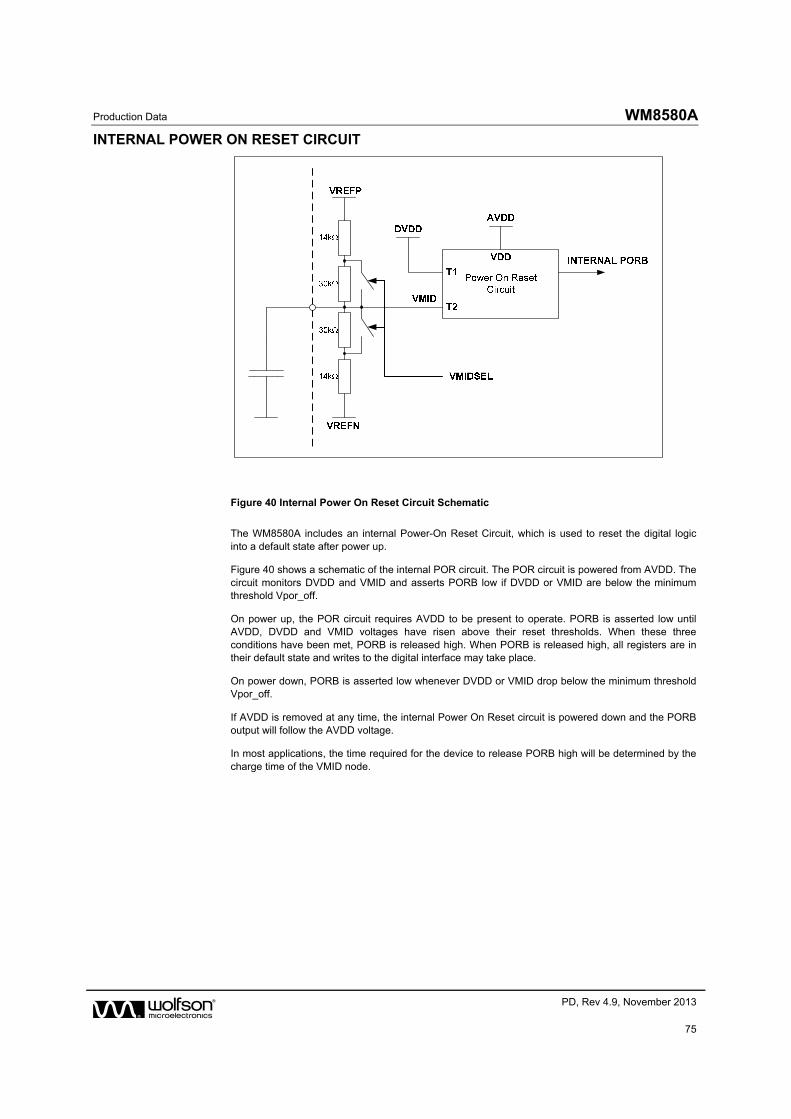
Production Data WM8580A
w PD, Rev 4.9, November 2013
75
INTERNAL POWER ON RESET CIRCUIT
Figure 40 Internal Power On Reset Circuit Schematic
The WM8580A includes an internal Power-On Reset Circuit, which is used to reset the digital logic into a default state after power up.
Figure 40 shows a schematic of the internal POR circuit. The POR circuit is powered from AVDD. The circuit monitors DVDD and VMID and asserts PORB low if DVDD or VMID are below the minimum threshold Vpor_off.
On power up, the POR circuit requires AVDD to be present to operate. PORB is asserted low until AVDD, DVDD and VMID voltages have risen above their reset thresholds. When these three conditions have been met, PORB is released high. When PORB is released high, all registers are in their default state and writes to the digital interface may take place.
On power down, PORB is asserted low whenever DVDD or VMID drop below the minimum threshold Vpor_off.
If AVDD is removed at any time, the internal Power On Reset circuit is powered down and the PORB output will follow the AVDD voltage.
In most applications, the time required for the device to release PORB high will be determined by the charge time of the VMID node.
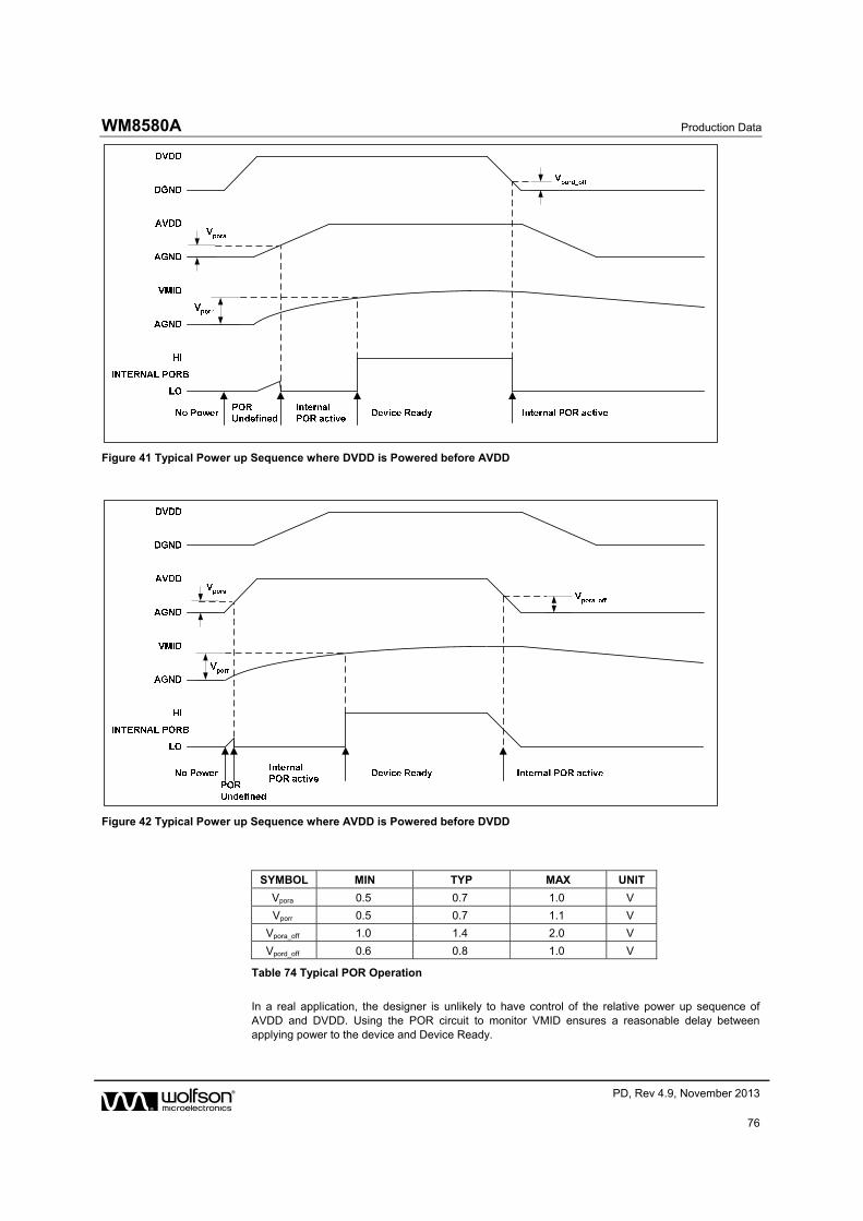
WM8580A Production Data
w PD, Rev 4.9, November 2013
76
Figure 41 Typical Power up Sequence where DVDD is Powered before AVDD
Figure 42 Typical Power up Sequence where AVDD is Powered before DVDD
SYMBOL MIN TYP MAX UNIT
Vpora 0.5 0.7 1.0 V
Vporr 0.5 0.7 1.1 V
Vpora_off 1.0 1.4 2.0 V
Vpord_off 0.6 0.8 1.0 V
Table 74 Typical POR Operation
In a real application, the designer is unlikely to have control of the relative power up sequence of AVDD and DVDD. Using the POR circuit to monitor VMID ensures a reasonable delay between applying power to the device and Device Ready.
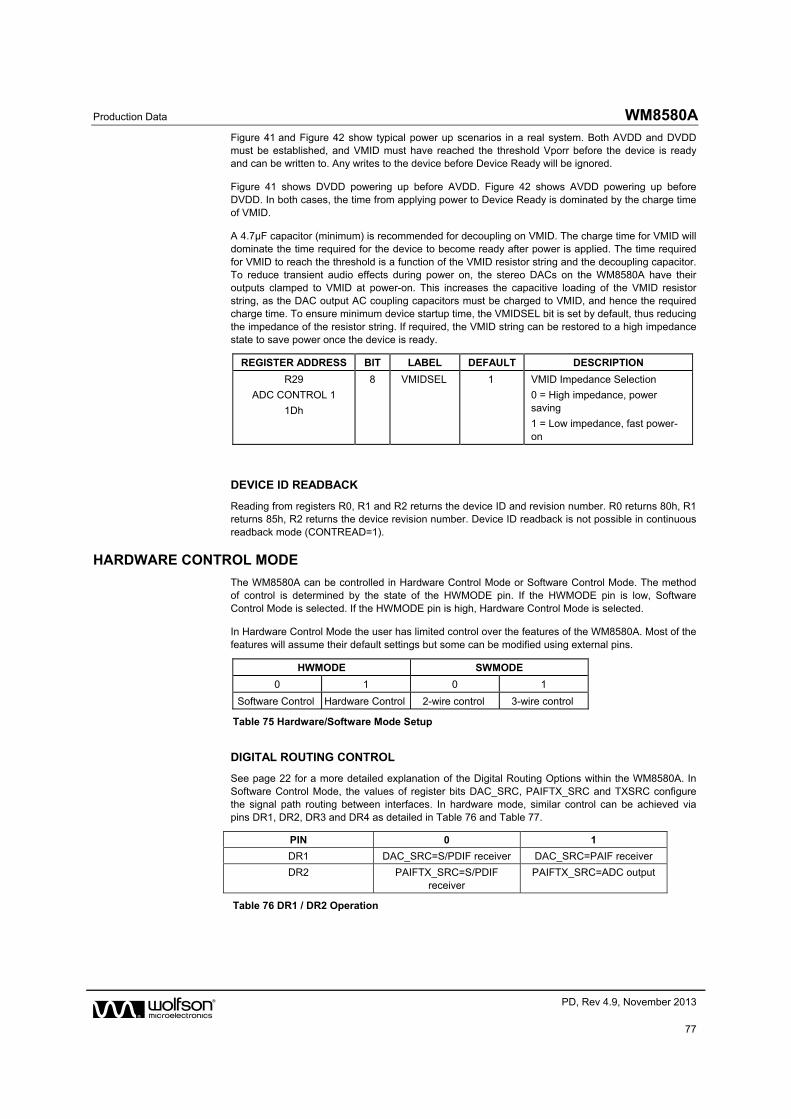
Production Data WM8580A
w PD, Rev 4.9, November 2013
77
Figure 41 and Figure 42 show typical power up scenarios in a real system. Both AVDD and DVDD must be established, and VMID must have reached the threshold Vporr before the device is ready and can be written to. Any writes to the device before Device Ready will be ignored.
Figure 41 shows DVDD powering up before AVDD. Figure 42 shows AVDD powering up before DVDD. In both cases, the time from applying power to Device Ready is dominated by the charge time of VMID.
A 4.7µF capacitor (minimum) is recommended for decoupling on VMID. The charge time for VMID will dominate the time required for the device to become ready after power is applied. The time required for VMID to reach the threshold is a function of the VMID resistor string and the decoupling capacitor. To reduce transient audio effects during power on, the stereo DACs on the WM8580A have their outputs clamped to VMID at power-on. This increases the capacitive loading of the VMID resistor string, as the DAC output AC coupling capacitors must be charged to VMID, and hence the required charge time. To ensure minimum device startup time, the VMIDSEL bit is set by default, thus reducing the impedance of the resistor string. If required, the VMID string can be restored to a high impedance state to save power once the device is ready.
REGISTER ADDRESS BIT LABEL DEFAULT DESCRIPTION
R29
ADC CONTROL 1
1Dh
8 VMIDSEL 1 VMID Impedance Selection
0 = High impedance, power saving
1 = Low impedance, fast power-on
DEVICE ID READBACK
Reading from registers R0, R1 and R2 returns the device ID and revision number. R0 returns 80h, R1 returns 85h, R2 returns the device revision number. Device ID readback is not possible in continuous readback mode (CONTREAD=1).
HARDWARE CONTROL MODE
The WM8580A can be controlled in Hardware Control Mode or Software Control Mode. The method of control is determined by the state of the HWMODE pin. If the HWMODE pin is low, Software Control Mode is selected. If the HWMODE pin is high, Hardware Control Mode is selected.
In Hardware Control Mode the user has limited control over the features of the WM8580A. Most of the features will assume their default settings but some can be modified using external pins.
HWMODE SWMODE
0 1 0 1
Software Control Hardware Control 2-wire control 3-wire control
Table 75 Hardware/Software Mode Setup
DIGITAL ROUTING CONTROL
See page 22 for a more detailed explanation of the Digital Routing Options within the WM8580A. In Software Control Mode, the values of register bits DAC_SRC, PAIFTX_SRC and TXSRC configure the signal path routing between interfaces. In hardware mode, similar control can be achieved via pins DR1, DR2, DR3 and DR4 as detailed in Table 76 and Table 77.
PIN 0 1
DR1 DAC_SRC=S/PDIF receiver DAC_SRC=PAIF receiver
DR2 PAIFTX_SRC=S/PDIF receiver
PAIFTX_SRC=ADC output
Table 76 DR1 / DR2 Operation
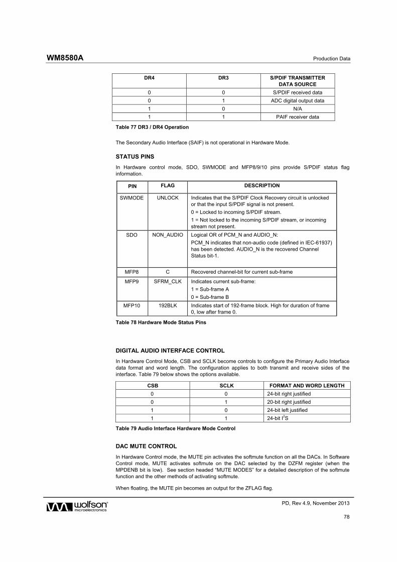
WM8580A Production Data
w PD, Rev 4.9, November 2013
78
DR4 DR3 S/PDIF TRANSMITTER
DATA SOURCE
0 0 S/PDIF received data
0 1 ADC digital output data
1 0 N/A
1 1 PAIF receiver data
Table 77 DR3 / DR4 Operation
The Secondary Audio Interface (SAIF) is not operational in Hardware Mode.
STATUS PINS
In Hardware control mode, SDO, SWMODE and MFP8/9/10 pins provide S/PDIF status flag information.
PIN FLAG DESCRIPTION
SWMODE UNLOCK Indicates that the S/PDIF Clock Recovery circuit is unlocked or that the input S/PDIF signal is not present.
0 = Locked to incoming S/PDIF stream.
1 = Not locked to the incoming S/PDIF stream, or incoming stream not present.
SDO NON_AUDIO Logical OR of PCM_N and AUDIO_N:
PCM_N indicates that non-audio code (defined in IEC-61937) has been detected. AUDIO_N is the recovered Channel Status bit-1.
MFP8 C Recovered channel-bit for current sub-frame
MFP9 SFRM_CLK Indicates current sub-frame:
1 = Sub-frame A
0 = Sub-frame B
MFP10 192BLK Indicates start of 192-frame block. High for duration of frame 0, low after frame 0.
Table 78 Hardware Mode Status Pins
DIGITAL AUDIO INTERFACE CONTROL
In Hardware Control Mode, CSB and SCLK become controls to configure the Primary Audio Interface data format and word length. The configuration applies to both transmit and receive sides of the interface. Table 79 below shows the options available.
CSB SCLK FORMAT AND WORD LENGTH
0 0 24-bit right justified
0 1 20-bit right justified
1 0 24-bit left justified
1 1 24-bit I2S
Table 79 Audio Interface Hardware Mode Control
DAC MUTE CONTROL
In Hardware Control mode, the MUTE pin activates the softmute function on all the DACs. In Software Control mode, MUTE activates softmute on the DAC selected by the DZFM register (when the MPDENB bit is low). See section headed “MUTE MODES” for a detailed description of the softmute function and the other methods of activating softmute.
When floating, the MUTE pin becomes an output for the ZFLAG flag.
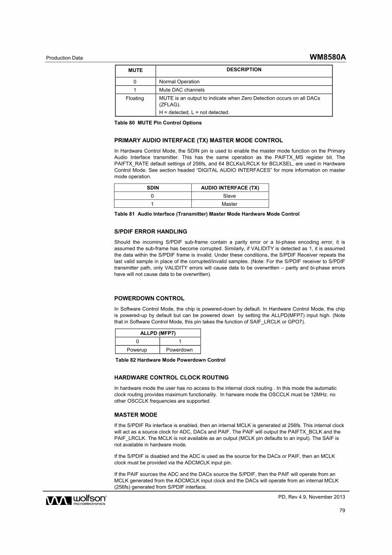
Production Data WM8580A
w PD, Rev 4.9, November 2013
79
MUTE DESCRIPTION
0 Normal Operation
1 Mute DAC channels
Floating MUTE is an output to indicate when Zero Detection occurs on all DACs (ZFLAG).
H = detected, L = not detected.
Table 80 MUTE Pin Control Options
PRIMARY AUDIO INTERFACE (TX) MASTER MODE CONTROL
In Hardware Control Mode, the SDIN pin is used to enable the master mode function on the Primary Audio Interface transmitter. This has the same operation as the PAIFTX_MS register bit. The PAIFTX_RATE default settings of 256fs, and 64 BCLKs/LRCLK for BCLKSEL, are used in Hardware Control Mode. See section headed “DIGITAL AUDIO INTERFACES” for more information on master mode operation.
SDIN AUDIO INTERFACE (TX)
0 Slave
1 Master
Table 81 Audio Interface (Transmitter) Master Mode Hardware Mode Control
S/PDIF ERROR HANDLING
Should the incoming S/PDIF sub-frame contain a parity error or a bi-phase encoding error, it is assumed the sub-frame has become corrupted. Similarly, if VALIDITY is detected as 1, it is assumed the data within the S/PDIF frame is invalid. Under these conditions, the S/PDIF Receiver repeats the last valid sample in place of the corrupted/invalid samples. (Note: For the S/PDIF receiver to S/PDIF transmitter path, only VALIDITY errors will cause data to be overwritten – parity and bi-phase errors have will not cause data to be overwritten).
POWERDOWN CONTROL
In Software Control Mode, the chip is powered-down by default. In Hardware Control Mode, the chip is powered-up by default but can be powered down by setting the ALLPD(MFP7) input high. (Note that in Software Control Mode, this pin takes the function of SAIF_LRCLK or GPO7).
ALLPD (MFP7)
0 1
Powerup Powerdown
Table 82 Hardware Mode Powerdown Control
HARDWARE CONTROL CLOCK ROUTING
In hardware mode the user has no access to the internal clock routing . In this mode the automatic clock routing provides maximum functionality. In harware mode the OSCCLK must be 12MHz. no other OSCCLK frequencies are supported.
MASTER MODE
If the S/PDIF Rx interface is enabled, then an internal MCLK is generated at 256fs. This internal clock will act as a source clock for ADC, DACs and PAIF. The PAIF will output the PAIFTX_BCLK and the PAIF_LRCLK. The MCLK is not available as an output (MCLK pin defaults to an input). The SAIF is not available in hardware mode.
If the S/PDIF is disabled and the ADC is used as the source for the DACs or PAIF, then an MCLK clock must be provided via the ADCMCLK input pin.
If the PAIF sources the ADC and the DACs source the S/PDIF, then the PAIF will operate from an MCLK generated from the ADCMCLK input clock and the DACs will operate from an internal MCLK (256fs) generated from S/PDIF interface.
WM8580A Production Data
w PD, Rev 4.9, November 2013
80
SLAVE MODE
If the S/PDIF Rx interface is enabled, then an internal MCLK is generated at 256fs. This internal clock will act as a source clock for ADC, DACs and PAIF. The user is required to supply input clocks to the PAIFTX_BCLK and the PAIF_LRCLK.
If the PAIF or DACs source the S/PDIF Rx interface then the PAIFTX_BCLK and the PAIF_LRCLK input clocks must be synchronous to clock driving the S/PDIF interface. If these clocks cannot be guaranteed synchronous then this mode of operation is not recommended.
If the PAIF sources the ADC data, then the user must supply input clocks to ADCCLK, PAIFTX_BCLK and the PAIF_LRCLK pins.
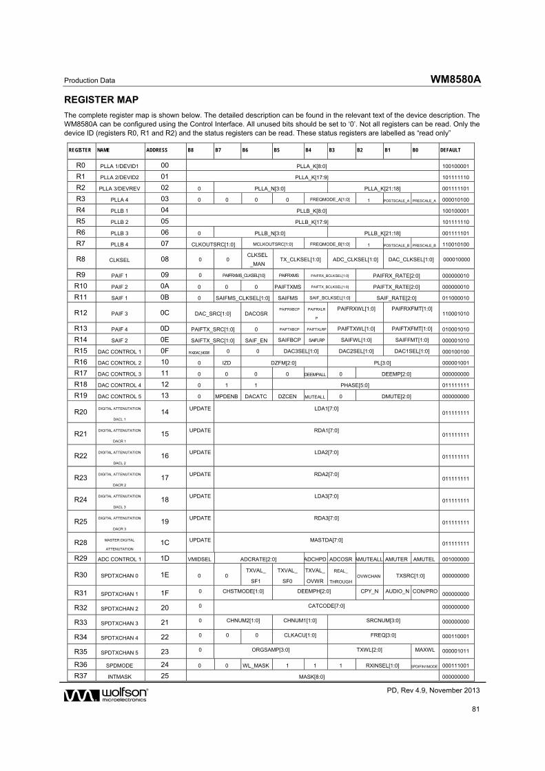
Production Data WM8580A
w PD, Rev 4.9, November 2013
81
REGISTER MAP
The complete register map is shown below. The detailed description can be found in the relevant text of the device description. The WM8580A can be configured using the Control Interface. All unused bits should be set to ‘0’. Not all registers can be read. Only the device ID (registers R0, R1 and R2) and the status registers can be read. These status registers are labelled as “read only”
REGISTER NAME ADDRESS B8 B7 B6 B5 B4 B3 B2 B1 B0 DEFAULT
R0 PLLA 1/DEVID1 00 PLLA_K[8:0] 100100001
R1 PLLA 2/DEVID2 01 PLLA_K[17:9] 101111110
R2 PLLA 3/DEVREV 02 0 PLLA_N[3:0] PLLA_K[21:18] 001111101
R3 PLLA 4 03 0 0 0 0 FREQMODE_A[1:0] 1 POSTSCALE_A PRESCALE_A 000010100
R4 PLLB 1 04 PLLB_K[8:0] 100100001
R5 PLLB 2 05 PLLB_K[17:9] 101111110
R6 PLLB 3 06 0 PLLB_N[3:0] PLLB_K[21:18] 001111101
R7 PLLB 4 07 CLKOUTSRC[1:0] MCLKOUTSRC[1:0] FREQMODE_B[1:0] 1 POSTSCALE_B PRESCALE_B 110010100
R8 CLKSEL 08 0 0 CLKSEL
_MAN TX_CLKSEL[1:0] ADC_CLKSEL[1:0] DAC_CLKSEL[1:0] 000010000
R9 PAIF 1 09 0 PAIFRXMS_CLKSEL[1:0] PAIFRXMS PAIFRX_BCLKSEL[1:0] PAIFRX_RATE[2:0] 000000010
R10 PAIF 2 0A 0 0 0 PAIFTXMS PAIFTX_BCLKSEL[1:0] PAIFTX_RATE[2:0] 000000010
R11 SAIF 1 0B 0 SAIFMS_CLKSEL[1:0] SAIFMS SAIF_BCLKSEL[1:0] SAIF_RATE[2:0] 011000010
R12 PAIF 3 0C DAC_SRC[1:0] DACOSR PAIFRXBCP PAIFRXLR
P
PAIFRXWL[1:0] PAIFRXFMT[1:0] 110001010
R13 PAIF 4 0D PAIFTX_SRC[1:0] 0 PAIFTXBCP PAIFTXLRP PAIFTXWL[1:0] PAIFTXFMT[1:0] 010001010
R14 SAIF 2 0E SAIFTX_SRC[1:0] SAIF_EN SAIFBCP SAIFLRP SAIFWL[1:0] SAIFFMT[1:0] 000001010
R15 DAC CONTROL 1 0F RX2DAC_MODE 0 0 DAC3SEL[1:0] DAC2SEL[1:0] DAC1SEL[1:0] 000100100
R16 DAC CONTROL 2 10 0 IZD DZFM[2:0] PL[3:0] 000001001
R17 DAC CONTROL 3 11 0 0 0 0 DEEMPALL 0 DEEMP[2:0] 000000000
R18 DAC CONTROL 4 12 0 1 1 PHASE[5:0] 011111111
R19 DAC CONTROL 5 13 0 MPDENB DACATC DZCEN MUTEALL 0 DMUTE[2:0] 000000000
R20 DIGITAL ATTENUTATION
DACL 1
14 UPDATE LDA1[7:0]
011111111
R21 DIGITAL ATTENUTATION
DACR 1
15 UPDATE RDA1[7:0]
011111111
R22 DIGITAL ATTENUTATION
DACL 2
16 UPDATE LDA2[7:0]
011111111
R23 DIGITAL ATTENUTATION
DACR 2
17 UPDATE RDA2[7:0]
011111111
R24 DIGITAL ATTENUTATION
DACL 3
18 UPDATE LDA3[7:0]
011111111
R25 DIGITAL ATTENUTATION
DACR 3
19 UPDATE RDA3[7:0]
011111111
R28 MASTER DIGITAL
ATTENUTATION
1C UPDATE MASTDA[7:0] 011111111
R29 ADC CONTROL 1 1D VMIDSEL ADCRATE[2:0] ADCHPD ADCOSR AMUTEALL AMUTER AMUTEL 001000000
R30 SPDTXCHAN 0 1E 0 0 TXVAL_
SF1
TXVAL_
SF0
TXVAL_
OVWR
REAL_
THROUGH OVWCHAN TXSRC[1:0] 000000000
R31 SPDTXCHAN 1 1F 0 CHSTMODE[1:0] DEEMPH[2:0] CPY_N AUDIO_N CON/PRO 000000000
R32 SPDTXCHAN 2 20 0 CATCODE[7:0] 000000000
R33 SPDTXCHAN 3 21 0 CHNUM2[1:0] CHNUM1[1:0] SRCNUM[3:0] 000000000
R34 SPDTXCHAN 4 22 0 0 0 CLKACU[1:0] FREQ[3:0] 000110001
R35 SPDTXCHAN 5 23 0 ORGSAMP[3:0] TXWL[2:0] MAXWL 000001011
R36 SPDMODE 24 0 0 WL_MASK 1 1 1 RXINSEL[1:0] SPDIFIN1MODE 000111001
R37 INTMASK 25 MASK[8:0] 000000000
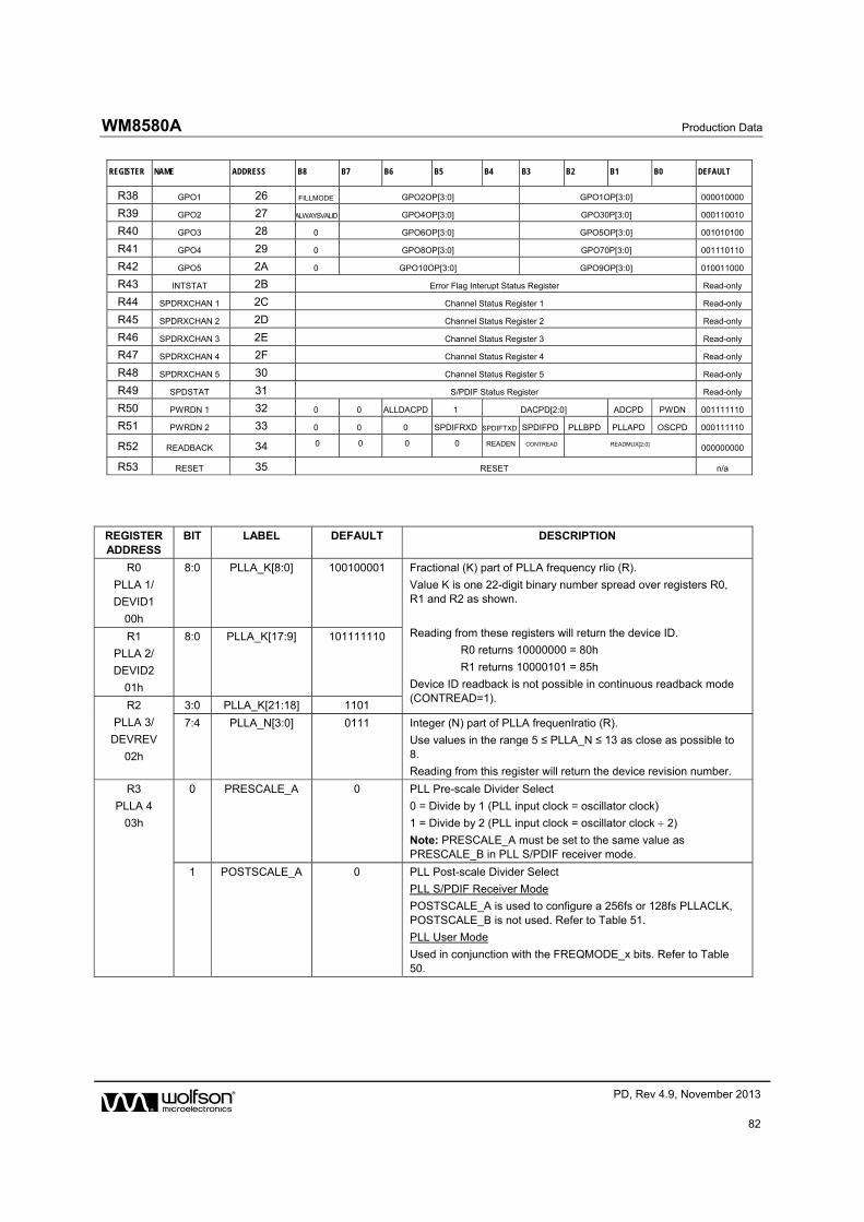
WM8580A Production Data
w PD, Rev 4.9, November 2013
82
REGISTER NAME ADDRESS B8 B7 B6 B5 B4 B3 B2 B1 B0 DEFAULT
R38 GPO1 26 FILLMODE GPO2OP[3:0] GPO1OP[3:0] 000010000
R39 GPO2 27 ALWAYSVALID GPO4OP[3:0] GPO30P[3:0] 000110010
R40 GPO3 28 0 GPO6OP[3:0] GPO5OP[3:0] 001010100
R41 GPO4 29 0 GPO8OP[3:0] GPO70P[3:0] 001110110
R42 GPO5 2A 0 GPO10OP[3:0] GPO9OP[3:0] 010011000
R43 INTSTAT 2B Error Flag Interupt Status Register Read-only
R44 SPDRXCHAN 1 2C Channel Status Register 1 Read-only
R45 SPDRXCHAN 2 2D Channel Status Register 2 Read-only
R46 SPDRXCHAN 3 2E Channel Status Register 3 Read-only
R47 SPDRXCHAN 4 2F Channel Status Register 4 Read-only
R48 SPDRXCHAN 5 30 Channel Status Register 5 Read-only
R49 SPDSTAT 31 S/PDIF Status Register Read-only
R50 PWRDN 1 32 0 0 ALLDACPD 1 DACPD[2:0] ADCPD PWDN 001111110
R51 PWRDN 2 33 0 0 0 SPDIFRXD SPDIFTXD SPDIFPD PLLBPD PLLAPD OSCPD 000111110
R52 READBACK 34 0 0 0 0 READEN CONTREAD READMUX[2:0] 000000000
R53 RESET 35 RESET n/a
REGISTER ADDRESS
BIT LABEL DEFAULT DESCRIPTION
R0
PLLA 1/
DEVID1
00h
8:0 PLLA_K[8:0] 100100001 Fractional (K) part of PLLA frequency rIio (R).
Value K is one 22-digit binary number spread over registers R0, R1 and R2 as shown.
Reading from these registers will return the device ID.
R0 returns 10000000 = 80h
R1 returns 10000101 = 85h
Device ID readback is not possible in continuous readback mode (CONTREAD=1).
R1
PLLA 2/
DEVID2
01h
8:0 PLLA_K[17:9] 101111110
R2
PLLA 3/
DEVREV
02h
3:0 PLLA_K[21:18] 1101
7:4 PLLA_N[3:0] 0111 Integer (N) part of PLLA frequenIratio (R).
Use values in the range 5 ≤ PLLA_N ≤ 13 as close as possible to 8.
Reading from this register will return the device revision number.
R3
PLLA 4
03h
0 PRESCALE_A 0 PLL Pre-scale Divider Select
0 = Divide by 1 (PLL input clock = oscillator clock)
1 = Divide by 2 (PLL input clock = oscillator clock 2)
Note: PRESCALE_A must be set to the same value as PRESCALE_B in PLL S/PDIF receiver mode.
1 POSTSCALE_A 0 PLL Post-scale Divider Select
PLL S/PDIF Receiver Mode
POSTSCALE_A is used to configure a 256fs or 128fs PLLACLK, POSTSCALE_B is not used. Refer to Table 51.
PLL User Mode
Used in conjunction with the FREQMODE_x bits. Refer to Table 50.
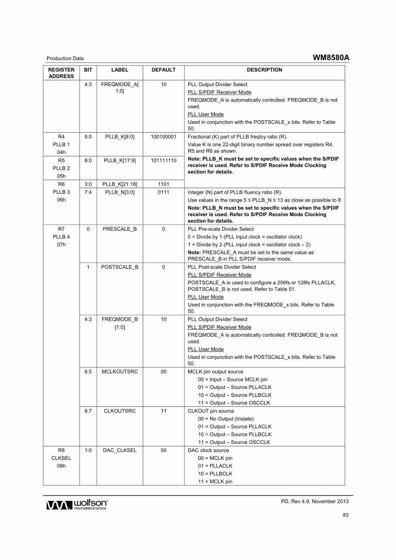
Production Data WM8580A
w PD, Rev 4.9, November 2013
83
REGISTER ADDRESS
BIT LABEL DEFAULT DESCRIPTION
4:3 FREQMODE_A[1:0]
10 PLL Output Divider Select
PLL S/PDIF Receiver Mode
FREQMODE_A is automatically controlled. FREQMODE_B is not used.
PLL User Mode
Used in conjunction with the POSTSCALE_x bits. Refer to Table 50.
R4
PLLB 1
04h
8:0 PLLB_K[8:0] 100100001 Fractional (K) part of PLLB freqIcy ratio (R).
Value K is one 22-digit binary number spread over registers R4, R5 and R6 as shown.
Note: PLLB_K must be set to specific values when the S/PDIF receiver is used. Refer to S/PDIF Receive Mode Clocking section for details.
R5
PLLB 2
05h
8:0 PLLB_K[17:9] 101111110
R6
PLLB 3
06h
3:0 PLLB_K[21:18] 1101
7:4 PLLB_N[3:0] 0111 Integer (N) part of PLLB fIuency ratio (R).
Use values in the range 5 ≤ PLLB_N ≤ 13 as close as possible to 8
Note: PLLB_N must be set to specific values when the S/PDIF receiver is used. Refer to S/PDIF Receive Mode Clocking section for details.
R7
PLLB 4
07h
0 PRESCALE_B 0 PLL Pre-scale Divider Select
0 = Divide by 1 (PLL input clock = oscillator clock)
1 = Divide by 2 (PLL input clock = oscillator clock 2)
Note: PRESCALE_A must be set to the same value as PRESCALE_B in PLL S/PDIF receiver mode.
1 POSTSCALE_B 0 PLL Post-scale Divider Select
PLL S/PDIF Receiver Mode
POSTSCALE_A is used to configure a 256fs or 128fs PLLACLK, POSTSCALE_B is not used. Refer to Table 51.
PLL User Mode
Used in conjunction with the FREQMODE_x bits. Refer to Table 50.
4:3 FREQMODE_B
[1:0]
10 PLL Output Divider Select
PLL S/PDIF Receiver Mode
FREQMODE_A is automatically controlled. FREQMODE_B is not used.
PLL User Mode
Used in conjunction with the POSTSCALE_x bits. Refer to Table 50.
6:5 MCLKOUTSRC 00 MCLK pin output source
00 = Input – Source MCLK pin
01 = Output – Source PLLACLK
10 = Output – Source PLLBCLK
11 = Output – Source OSCCLK
8:7 CLKOUTSRC 11 CLKOUT pin source
00 = No Output (tristate)
01 = Output – Source PLLACLK
10 = Output – Source PLLBCLK
11 = Output – Source OSCCLK
R8
CLKSEL
08h
1:0 DAC_CLKSEL 00 DAC clock source
00 = MCLK pin
01 = PLLACLK
10 = PLLBCLK
11 = MCLK pin
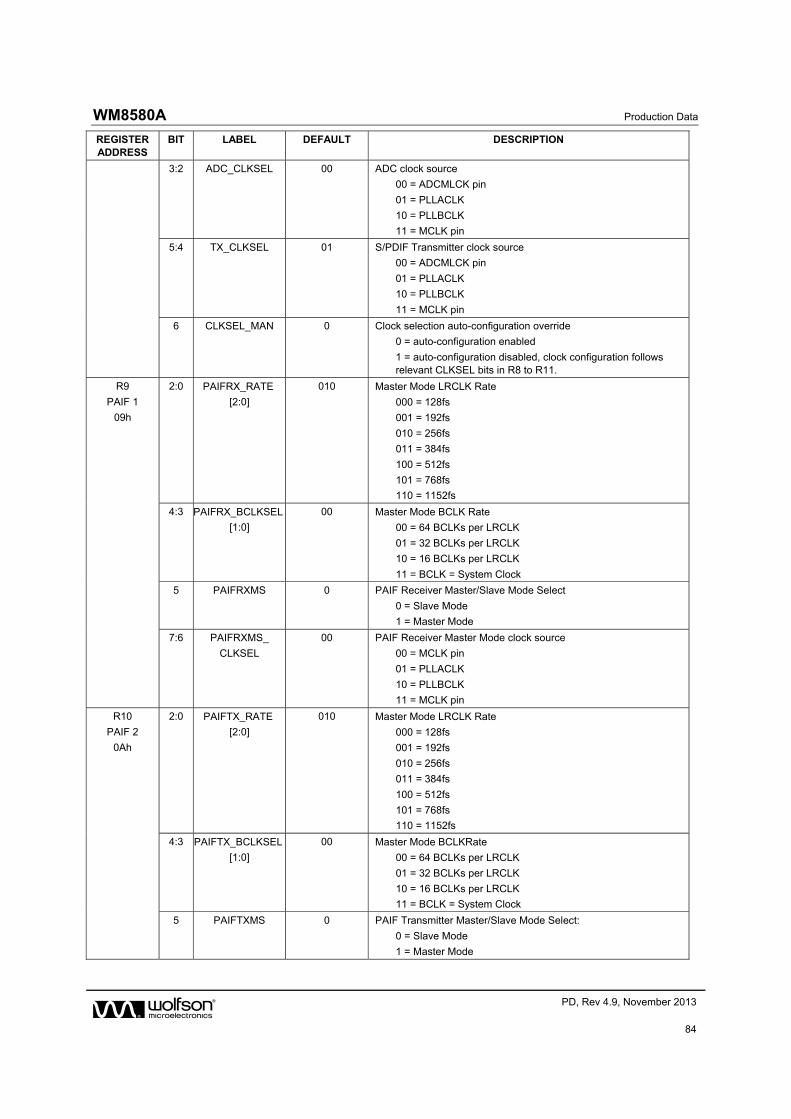
WM8580A Production Data
w PD, Rev 4.9, November 2013
84
REGISTER ADDRESS
BIT LABEL DEFAULT DESCRIPTION
3:2 ADC_CLKSEL 00 ADC clock source
00 = ADCMLCK pin
01 = PLLACLK
10 = PLLBCLK
11 = MCLK pin
5:4 TX_CLKSEL 01 S/PDIF Transmitter clock source
00 = ADCMLCK pin
01 = PLLACLK
10 = PLLBCLK
11 = MCLK pin
6 CLKSEL_MAN 0 Clock selection auto-configuration override
0 = auto-configuration enabled
1 = auto-configuration disabled, clock configuration follows relevant CLKSEL bits in R8 to R11.
R9
PAIF 1
09h
2:0 PAIFRX_RATE
[2:0]
010 Master Mode LRCLK Rate
000 = 128fs
001 = 192fs
010 = 256fs
011 = 384fs
100 = 512fs
101 = 768fs
110 = 1152fs
4:3 PAIFRX_BCLKSEL
[1:0]
00 Master Mode BCLK Rate
00 = 64 BCLKs per LRCLK
01 = 32 BCLKs per LRCLK
10 = 16 BCLKs per LRCLK
11 = BCLK = System Clock
5 PAIFRXMS 0 PAIF Receiver Master/Slave Mode Select
0 = Slave Mode
1 = Master Mode
7:6 PAIFRXMS_
CLKSEL
00 PAIF Receiver Master Mode clock source
00 = MCLK pin
01 = PLLACLK
10 = PLLBCLK
11 = MCLK pin
R10
PAIF 2
0Ah
2:0 PAIFTX_RATE
[2:0]
010 Master Mode LRCLK Rate
000 = 128fs
001 = 192fs
010 = 256fs
011 = 384fs
100 = 512fs
101 = 768fs
110 = 1152fs
4:3 PAIFTX_BCLKSEL
[1:0]
00 Master Mode BCLKRate
00 = 64 BCLKs per LRCLK
01 = 32 BCLKs per LRCLK
10 = 16 BCLKs per LRCLK
11 = BCLK = System Clock
5 PAIFTXMS 0 PAIF Transmitter Master/Slave Mode Select:
0 = Slave Mode
1 = Master Mode
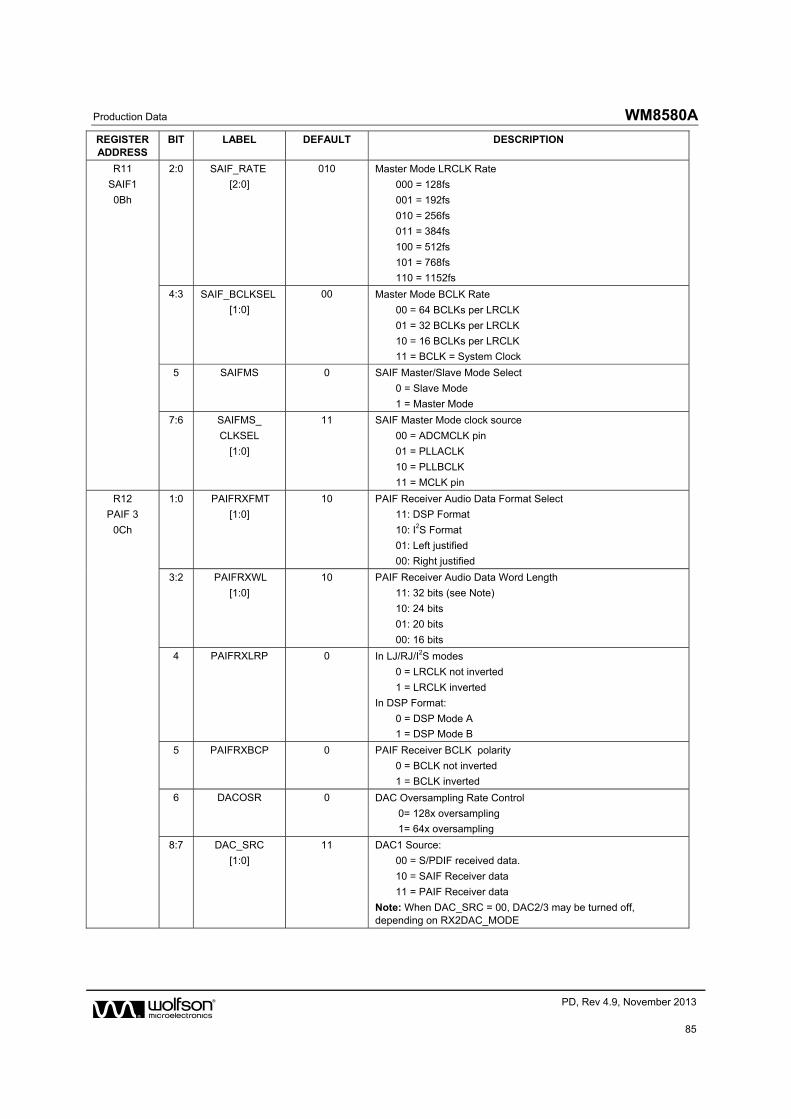
Production Data WM8580A
w PD, Rev 4.9, November 2013
85
REGISTER ADDRESS
BIT LABEL DEFAULT DESCRIPTION
R11
SAIF1
0Bh
2:0 SAIF_RATE
[2:0]
010 Master Mode LRCLK Rate
000 = 128fs
001 = 192fs
010 = 256fs
011 = 384fs
100 = 512fs
101 = 768fs
110 = 1152fs
4:3 SAIF_BCLKSEL
[1:0]
00 Master Mode BCLK Rate
00 = 64 BCLKs per LRCLK
01 = 32 BCLKs per LRCLK
10 = 16 BCLKs per LRCLK
11 = BCLK = System Clock
5 SAIFMS 0 SAIF Master/Slave Mode Select
0 = Slave Mode
1 = Master Mode
7:6 SAIFMS_
CLKSEL
[1:0]
11 SAIF Master Mode clock source
00 = ADCMCLK pin
01 = PLLACLK
10 = PLLBCLK
11 = MCLK pin
R12
PAIF 3
0Ch
1:0 PAIFRXFMT
[1:0]
10 PAIF Receiver Audio Data Format Select
11: DSP Format
10: I2S Format
01: Left justified
00: Right justified
3:2 PAIFRXWL
[1:0]
10 PAIF Receiver Audio Data Word Length
11: 32 bits (see Note)
10: 24 bits
01: 20 bits
00: 16 bits
4 PAIFRXLRP 0 In LJ/RJ/I2S modes
0 = LRCLK not inverted
1 = LRCLK inverted
In DSP Format:
0 = DSP Mode A
1 = DSP Mode B
5 PAIFRXBCP 0 PAIF Receiver BCLK polarity
0 = BCLK not inverted
1 = BCLK inverted
6 DACOSR 0 DAC Oversampling Rate Control
0= 128x oversampling
1= 64x oversampling
8:7 DAC_SRC
[1:0]
11 DAC1 Source:
00 = S/PDIF received data.
10 = SAIF Receiver data
11 = PAIF Receiver data
Note: When DAC_SRC = 00, DAC2/3 may be turned off, depending on RX2DAC_MODE
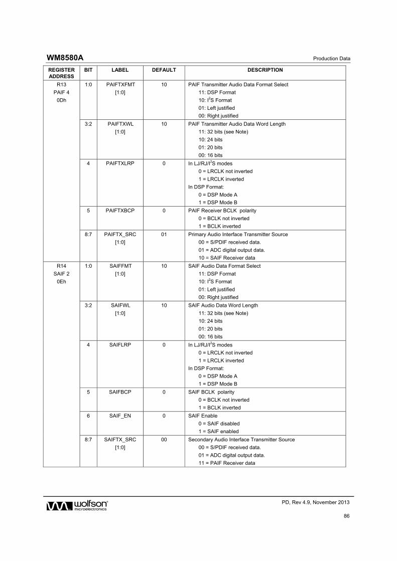
WM8580A Production Data
w PD, Rev 4.9, November 2013
86
REGISTER ADDRESS
BIT LABEL DEFAULT DESCRIPTION
R13
PAIF 4
0Dh
1:0 PAIFTXFMT
[1:0]
10 PAIF Transmitter Audio Data Format Select
11: DSP Format
10: I2S Format
01: Left justified
00: Right justified
3:2 PAIFTXWL
[1:0]
10 PAIF Transmitter Audio Data Word Length
11: 32 bits (see Note)
10: 24 bits
01: 20 bits
00: 16 bits
4 PAIFTXLRP 0 In LJ/RJ/I2S modes
0 = LRCLK not inverted
1 = LRCLK inverted
In DSP Format:
0 = DSP Mode A
1 = DSP Mode B
5 PAIFTXBCP 0 PAIF Receiver BCLK polarity
0 = BCLK not inverted
1 = BCLK inverted
8:7 PAIFTX_SRC
[1:0]
01 Primary Audio Interface Transmitter Source
00 = S/PDIF received data.
01 = ADC digital output data.
10 = SAIF Receiver data
R14
SAIF 2
0Eh
1:0 SAIFFMT
[1:0]
10 SAIF Audio Data Format Select
11: DSP Format
10: I2S Format
01: Left justified
00: Right justified
3:2 SAIFWL
[1:0]
10 SAIF Audio Data Word Length
11: 32 bits (see Note)
10: 24 bits
01: 20 bits
00: 16 bits
4 SAIFLRP 0 In LJ/RJ/I2S modes
0 = LRCLK not inverted
1 = LRCLK inverted
In DSP Format:
0 = DSP Mode A
1 = DSP Mode B
5 SAIFBCP 0 SAIF BCLK polarity
0 = BCLK not inverted
1 = BCLK inverted
6 SAIF_EN 0 SAIF Enable
0 = SAIF disabled
1 = SAIF enabled
8:7 SAIFTX_SRC
[1:0]
00 Secondary Audio Interface Transmitter Source
00 = S/PDIF received data.
01 = ADC digital output data.
11 = PAIF Receiver data
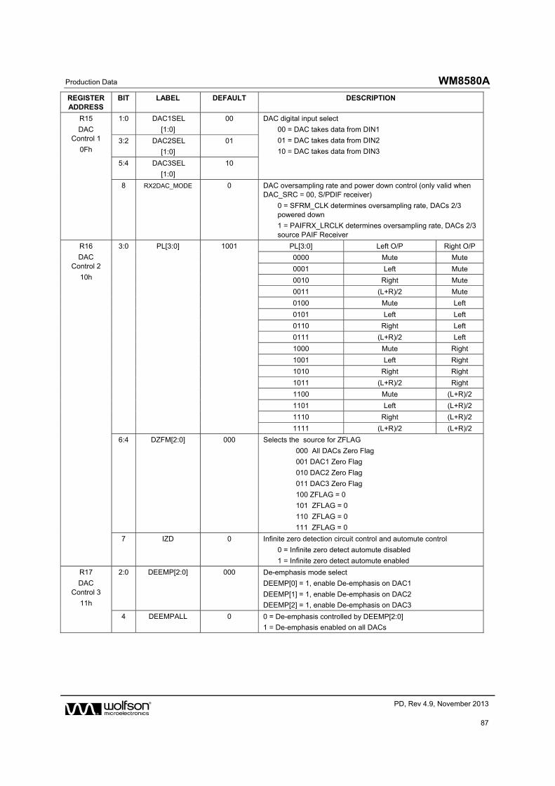
Production Data WM8580A
w PD, Rev 4.9, November 2013
87
REGISTER ADDRESS
BIT LABEL DEFAULT DESCRIPTION
R15
DAC Control 1
0Fh
1:0 DAC1SEL
[1:0]
00 DAC digital input select
00 = DAC takes data from DIN1
01 = DAC takes data from DIN2
10 = DAC takes data from DIN3
3:2 DAC2SEL
[1:0]
01
5:4 DAC3SEL
[1:0]
10
8 RX2DAC_MODE 0 DAC oversampling rate and power down control (only valid when DAC_SRC = 00, S/PDIF receiver)
0 = SFRM_CLK determines oversampling rate, DACs 2/3 powered down
1 = PAIFRX_LRCLK determines oversampling rate, DACs 2/3 source PAIF Receiver
R16
DAC Control 2
10h
3:0 PL[3:0] 1001 PL[3:0] Left O/P Right O/P
0000 Mute Mute
0001 Left Mute
0010 Right Mute
0011 (L+R)/2 Mute
0100 Mute Left
0101 Left Left
0110 Right Left
0111 (L+R)/2 Left
1000 Mute Right
1001 Left Right
1010 Right Right
1011 (L+R)/2 Right
1100 Mute (L+R)/2
1101 Left (L+R)/2
1110 Right (L+R)/2
1111 (L+R)/2 (L+R)/2
6:4 DZFM[2:0] 000 Selects the source for ZFLAG
000 All DACs Zero Flag
001 DAC1 Zero Flag
010 DAC2 Zero Flag
011 DAC3 Zero Flag
100 ZFLAG = 0
101 ZFLAG = 0
110 ZFLAG = 0
111 ZFLAG = 0
7 IZD 0 Infinite zero detection circuit control and automute control
0 = Infinite zero detect automute disabled
1 = Infinite zero detect automute enabled
R17
DAC Control 3
11h
2:0 DEEMP[2:0] 000 De-emphasis mode select
DEEMP[0] = 1, enable De-emphasis on DAC1
DEEMP[1] = 1, enable De-emphasis on DAC2
DEEMP[2] = 1, enable De-emphasis on DAC3
4 DEEMPALL 0 0 = De-emphasis controlled by DEEMP[2:0]
1 = De-emphasis enabled on all DACs
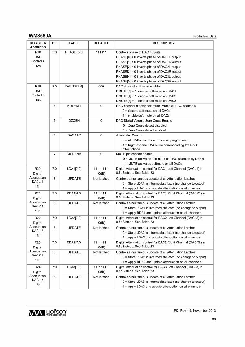
WM8580A Production Data
w PD, Rev 4.9, November 2013
88
REGISTER ADDRESS
BIT LABEL DEFAULT DESCRIPTION
R18
DAC Control 4
12h
5:0 PHASE [5:0] 111111 Controls phase of DAC outputs
PHASE[0] = 0 inverts phase of DAC1L output
PHASE[1] = 0 inverts phase of DAC1R output
PHASE[2] = 0 inverts phase of DAC2L output
PHASE[3] = 0 inverts phase of DAC2R output
PHASE[4] = 0 inverts phase of DAC3L output
PHASE[5] = 0 inverts phase of DAC3R output
R19
DAC Control 5
13h
2:0 DMUTE[2:0] 000 DAC channel soft mute enables
DMUTE[0] = 1, enable soft-mute on DAC1
DMUTE[1] = 1, enable soft-mute on DAC2
DMUTE[2] = 1, enable soft-mute on DAC3
4 MUTEALL 0 DAC channel master soft mute. Mutes all DAC channels
0 = disable soft-mute on all DACs
1 = enable soft-mute on all DACs
5 DZCEN 0 DAC Digital Volume Zero Cross Enable
0 = Zero Cross detect disabled
1 = Zero Cross detect enabled
6 DACATC 0 Attenuator Control
0 = All DACs use attenuations as programmed.
1 = Right channel DACs use corresponding left DAC attenuations
7 MPDENB 0 MUTE pin decode enable
0 = MUTE activates soft-mute on DAC selected by DZFM
1 = MUTE activates softmute on all DACs
R20
Digital Attenuation
DACL 1
14h
7:0 LDA1[7:0] 11111111
(0dB)
Digital Attenuation control for DAC1 Left Channel (DACL1) in 0.5dB steps. See Table 23
8 UPDATE Not latched Controls simultaneous update of all Attenuation Latches
0 = Store LDA1 in intermediate latch (no change to output)
1 = Apply LDA1 and update attenuation on all channels
R21
Digital Attenuation
DACR 1
15h
7:0 RDA1[6:0] 11111111
(0dB)
Digital Attenuation control for DAC1 Right Channel (DACR1) in 0.5dB steps. See Table 23
8 UPDATE Not latched Controls simultaneous update of all Attenuation Latches
0 = Store RDA1 in intermediate latch (no change to output)
1 = Apply RDA1 and update attenuation on all channels
R22
Digital Attenuation
DACL 2
16h
7:0 LDA2[7:0] 11111111
(0dB)
Digital Attenuation control for DAC2 Left Channel (DACL2) in 0.5dB steps. See Table 23
8 UPDATE Not latched Controls simultaneous update of all Attenuation Latches
0 = Store LDA2 in intermediate latch (no change to output)
1 = Apply LDA2 and update attenuation on all channels
R23
Digital Attenuation
DACR 2
17h
7:0 RDA2[7:0] 11111111
(0dB)
Digital Attenuation control for DAC2 Right Channel (DACR2) in 0.5dB steps. See Table 23
8 UPDATE Not latched Controls simultaneous update of all Attenuation Latches
0 = Store RDA2 in intermediate latch (no change to output)
1 = Apply RDA2 and update attenuation on all channels
R24
Digital Attenuation
DACL 3
18h
7:0 LDA3[7:0] 11111111
(0dB)
Digital Attenuation control for DAC3 Left Channel (DACL3) in 0.5dB steps. See Table 23
8 UPDATE Not latched Controls simultaneous update of all Attenuation Latches
0 = Store LDA3 in intermediate latch (no change to output)
1 = Apply LDA3 and update attenuation on all channels
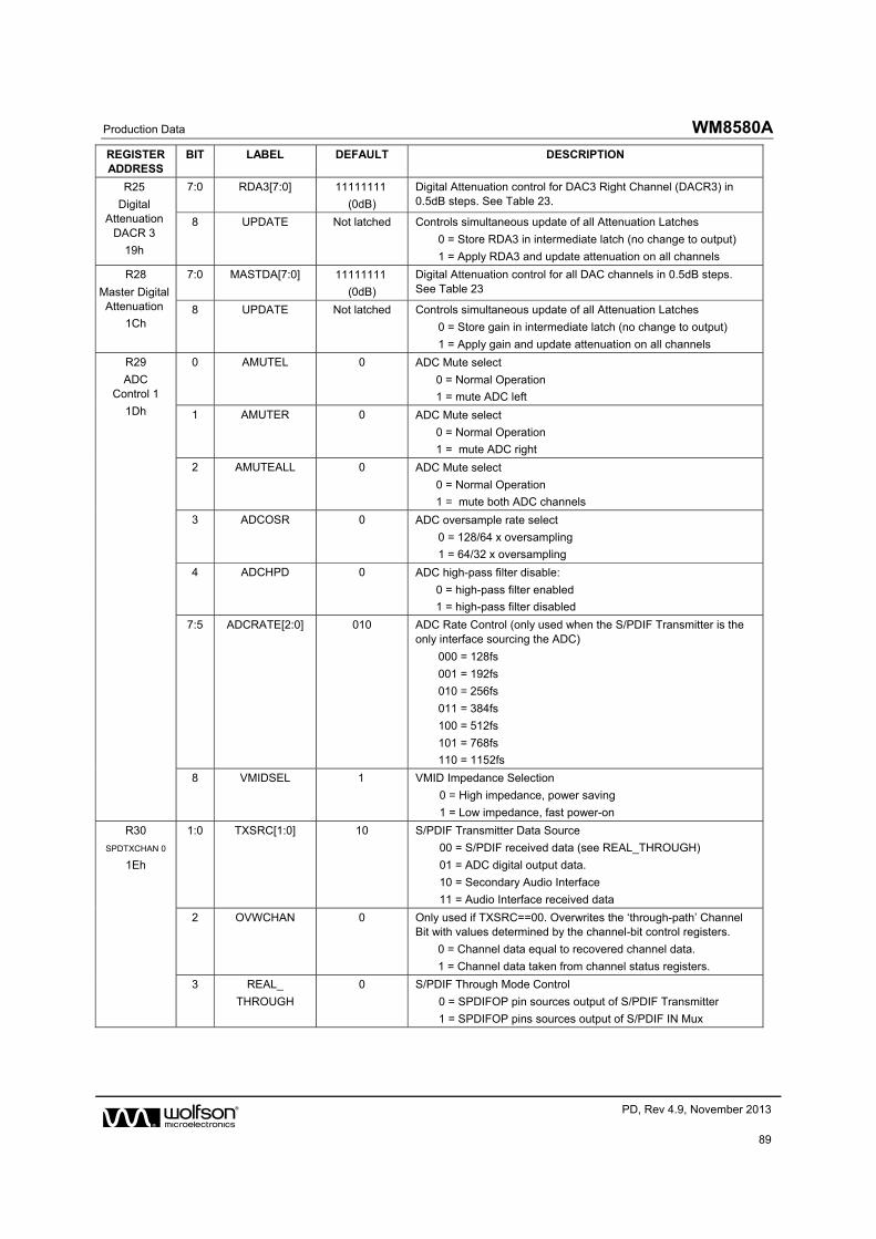
Production Data WM8580A
w PD, Rev 4.9, November 2013
89
REGISTER ADDRESS
BIT LABEL DEFAULT DESCRIPTION
R25
Digital Attenuation
DACR 3
19h
7:0 RDA3[7:0] 11111111
(0dB)
Digital Attenuation control for DAC3 Right Channel (DACR3) in 0.5dB steps. See Table 23.
8 UPDATE Not latched Controls simultaneous update of all Attenuation Latches
0 = Store RDA3 in intermediate latch (no change to output)
1 = Apply RDA3 and update attenuation on all channels
R28
Master Digital Attenuation
1Ch
7:0 MASTDA[7:0] 11111111
(0dB)
Digital Attenuation control for all DAC channels in 0.5dB steps. See Table 23
8 UPDATE Not latched Controls simultaneous update of all Attenuation Latches
0 = Store gain in intermediate latch (no change to output)
1 = Apply gain and update attenuation on all channels
R29
ADC Control 1
1Dh
0 AMUTEL 0 ADC Mute select
0 = Normal Operation
1 = mute ADC left
1 AMUTER 0 ADC Mute select
0 = Normal Operation
1 = mute ADC right
2 AMUTEALL 0 ADC Mute select
0 = Normal Operation
1 = mute both ADC channels
3 ADCOSR 0 ADC oversample rate select
0 = 128/64 x oversampling
1 = 64/32 x oversampling
4 ADCHPD 0 ADC high-pass filter disable:
0 = high-pass filter enabled
1 = high-pass filter disabled
7:5 ADCRATE[2:0] 010 ADC Rate Control (only used when the S/PDIF Transmitter is the only interface sourcing the ADC)
000 = 128fs
001 = 192fs
010 = 256fs
011 = 384fs
100 = 512fs
101 = 768fs
110 = 1152fs
8 VMIDSEL 1 VMID Impedance Selection
0 = High impedance, power saving
1 = Low impedance, fast power-on
R30
SPDTXCHAN 0
1Eh
1:0 TXSRC[1:0] 10 S/PDIF Transmitter Data Source
00 = S/PDIF received data (see REAL_THROUGH)
01 = ADC digital output data.
10 = Secondary Audio Interface
11 = Audio Interface received data
2 OVWCHAN 0 Only used if TXSRC==00. Overwrites the ‘through-path’ Channel Bit with values determined by the channel-bit control registers.
0 = Channel data equal to recovered channel data.
1 = Channel data taken from channel status registers.
3 REAL_
THROUGH
0 S/PDIF Through Mode Control
0 = SPDIFOP pin sources output of S/PDIF Transmitter
1 = SPDIFOP pins sources output of S/PDIF IN Mux
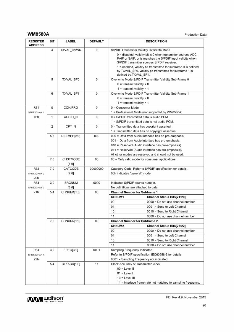
WM8580A Production Data
w PD, Rev 4.9, November 2013
90
REGISTER ADDRESS
BIT LABEL DEFAULT DESCRIPTION
4 TXVAL_OVWR 0 S/PDIF Transmitter Validity Overwrite Mode
0 = disabled, validity bit is 0 when transmitter sources ADC, PAIF or SAIF, or is matches the S/PDIF input validity when S/PDIF transmitter sources S/PDIF receiver.
1 = enabled, validity bit transmitted for subframe 0 is defined by TXVAL_SF0, validity bit transmitted for subframe 1 is defined by TXVAL_SF1.
5 TXVAL_SF0 0 Overwrite Mode S/PDIF Transmitter Validity Sub-Frame 0
0 = transmit validity = 0
1 = transmit validity = 1
6 TXVAL_SF1 0 Overwrite Mode S/PDIF Transmitter Validity Sub-Frame 1
0 = transmit validity = 0
1 = transmit validity = 1
R31
SPDTXCHAN 1
1Fh
0 CON/PRO 0 0 = Consumer Mode
1 = Professional Mode (not supported by WM8580A)
1 AUDIO_N 0 0 = S/PDIF transmitted data is audio PCM.
1 = S/PDIF transmitted data is not audio PCM.
2 CPY_N 0 0 = Transmitted data has copyright asserted.
1 = Transmitted data has no copyright assertion.
5:3 DEEMPH[2:0] 000 000 = Data from Audio interface has no pre-emphasis.
001 = Data from Audio interface has pre-emphasis.
010 = Reserved (Audio interface has pre-emphasis).
011 = Reserved (Audio interface has pre-emphasis).
All other modes are reserved and should not be used.
7:6 CHSTMODE
[1:0]
00 00 = Only valid mode for consumer applications.
R32
SPDTXCHAN 2
20h
7:0 CATCODE
[7:0]
00000000 Category Code. Refer to S/PDIF specification for details.
00h indicates “general” mode
R33
SPDTXCHAN 3
21h
3:0 SRCNUM
[3:0]
0000 Indicates S/PDIF source number.
No definitions are attached to data.
5:4 CHNUM1[1:0] 00 Channel Number for Subframe 1
CHNUM1 Channel Status Bits[21:20]
00 0000 = Do not use channel number
01 0001 = Send to Left Channel
10 0010 = Send to Right Channel
11 0000 = Do not use channel number
7:6 CHNUM2[1:0] 00 Channel Number for Subframe 2
CHNUM2 Channel Status Bits[23:22]
00 0000 = Do not use channel number
01 0001 = Send to Left Channel
10 0010 = Send to Right Channel
11 0000 = Do not use channel number
R34
SPDTXCHAN 4
22h
3:0 FREQ[3:0] 0001 Sampling Frequency Indicated.
Refer to S/PDIF specification IEC60958-3 for details.
0001 = Sampling Frequency not indicated.
5:4 CLKACU[1:0] 11 Clock Accuracy of Transmitted clock.
00 = Level II
01 = Level I
10 = Level III
11 = Interface frame rate not matched to sampling frequency.
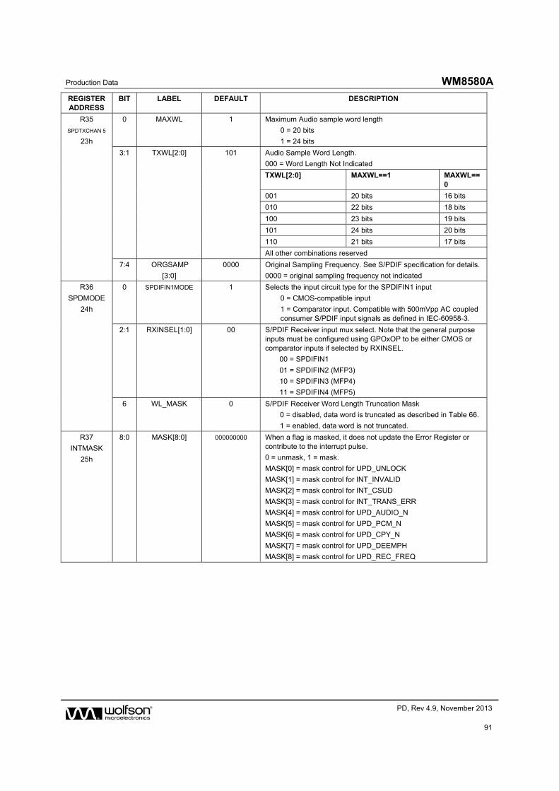
Production Data WM8580A
w PD, Rev 4.9, November 2013
91
REGISTER ADDRESS
BIT LABEL DEFAULT DESCRIPTION
R35
SPDTXCHAN 5
23h
0 MAXWL 1 Maximum Audio sample word length
0 = 20 bits
1 = 24 bits
3:1 TXWL[2:0] 101 Audio Sample Word Length.
000 = Word Length Not Indicated
TXWL[2:0] MAXWL==1 MAXWL==0
001 20 bits 16 bits
010 22 bits 18 bits
100 23 bits 19 bits
101 24 bits 20 bits
110 21 bits 17 bits
All other combinations reserved
7:4 ORGSAMP
[3:0]
0000 Original Sampling Frequency. See S/PDIF specification for details.
0000 = original sampling frequency not indicated
R36
SPDMODE
24h
0 SPDIFIN1MODE 1 Selects the input circuit type for the SPDIFIN1 input
0 = CMOS-compatible input
1 = Comparator input. Compatible with 500mVpp AC coupled consumer S/PDIF input signals as defined in IEC-60958-3.
2:1 RXINSEL[1:0] 00 S/PDIF Receiver input mux select. Note that the general purpose inputs must be configured using GPOxOP to be either CMOS or comparator inputs if selected by RXINSEL.
00 = SPDIFIN1
01 = SPDIFIN2 (MFP3)
10 = SPDIFIN3 (MFP4)
11 = SPDIFIN4 (MFP5)
6 WL_MASK 0 S/PDIF Receiver Word Length Truncation Mask
0 = disabled, data word is truncated as described in Table 66.
1 = enabled, data word is not truncated.
R37
INTMASK
25h
8:0 MASK[8:0] 000000000 When a flag is masked, it does not update the Error Register or contribute to the interrupt pulse.
0 = unmask, 1 = mask.
MASK[0] = mask control for UPD_UNLOCK
MASK[1] = mask control for INT_INVALID
MASK[2] = mask control for INT_CSUD
MASK[3] = mask control for INT_TRANS_ERR
MASK[4] = mask control for UPD_AUDIO_N
MASK[5] = mask control for UPD_PCM_N
MASK[6] = mask control for UPD_CPY_N
MASK[7] = mask control for UPD_DEEMPH
MASK[8] = mask control for UPD_REC_FREQ
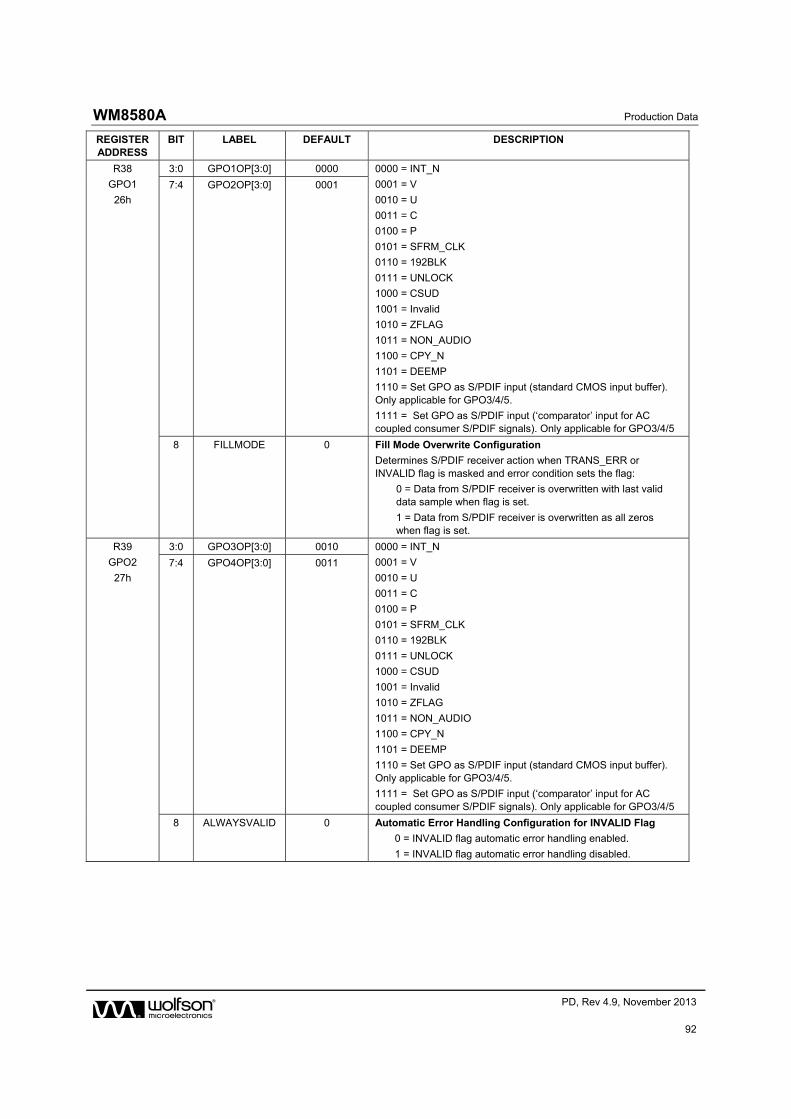
WM8580A Production Data
w PD, Rev 4.9, November 2013
92
REGISTER ADDRESS
BIT LABEL DEFAULT DESCRIPTION
R38
GPO1
26h
3:0 GPO1OP[3:0] 0000 0000 = INT_N
0001 = V
0010 = U
0011 = C
0100 = P
0101 = SFRM_CLK
0110 = 192BLK
0111 = UNLOCK
1000 = CSUD
1001 = Invalid
1010 = ZFLAG
1011 = NON_AUDIO
1100 = CPY_N
1101 = DEEMP
1110 = Set GPO as S/PDIF input (standard CMOS input buffer). Only applicable for GPO3/4/5.
1111 = Set GPO as S/PDIF input (‘comparator’ input for AC coupled consumer S/PDIF signals). Only applicable for GPO3/4/5
7:4 GPO2OP[3:0] 0001
8 FILLMODE 0 Fill Mode Overwrite Configuration
Determines S/PDIF receiver action when TRANS_ERR or INVALID flag is masked and error condition sets the flag:
0 = Data from S/PDIF receiver is overwritten with last valid data sample when flag is set.
1 = Data from S/PDIF receiver is overwritten as all zeros when flag is set.
R39
GPO2
27h
3:0 GPO3OP[3:0] 0010 0000 = INT_N
0001 = V
0010 = U
0011 = C
0100 = P
0101 = SFRM_CLK
0110 = 192BLK
0111 = UNLOCK
1000 = CSUD
1001 = Invalid
1010 = ZFLAG
1011 = NON_AUDIO
1100 = CPY_N
1101 = DEEMP
1110 = Set GPO as S/PDIF input (standard CMOS input buffer). Only applicable for GPO3/4/5.
1111 = Set GPO as S/PDIF input (‘comparator’ input for AC coupled consumer S/PDIF signals). Only applicable for GPO3/4/5
7:4 GPO4OP[3:0] 0011
8 ALWAYSVALID 0 Automatic Error Handling Configuration for INVALID Flag
0 = INVALID flag automatic error handling enabled.
1 = INVALID flag automatic error handling disabled.
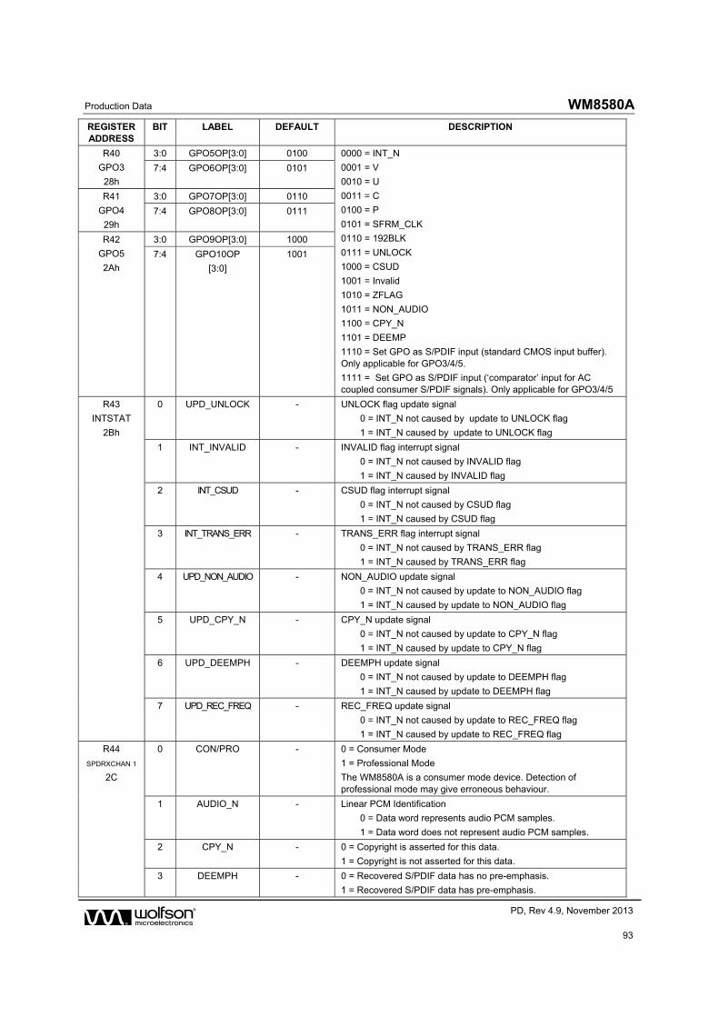
Production Data WM8580A
w PD, Rev 4.9, November 2013
93
REGISTER ADDRESS
BIT LABEL DEFAULT DESCRIPTION
R40
GPO3
28h
3:0 GPO5OP[3:0] 0100 0000 = INT_N
0001 = V
0010 = U
0011 = C
0100 = P
0101 = SFRM_CLK
0110 = 192BLK
0111 = UNLOCK
1000 = CSUD
1001 = Invalid
1010 = ZFLAG
1011 = NON_AUDIO
1100 = CPY_N
1101 = DEEMP
1110 = Set GPO as S/PDIF input (standard CMOS input buffer). Only applicable for GPO3/4/5.
1111 = Set GPO as S/PDIF input (‘comparator’ input for AC coupled consumer S/PDIF signals). Only applicable for GPO3/4/5
7:4 GPO6OP[3:0] 0101
R41
GPO4
29h
3:0 GPO7OP[3:0] 0110
7:4 GPO8OP[3:0] 0111
R42
GPO5
2Ah
3:0 GPO9OP[3:0] 1000
7:4 GPO10OP
[3:0]
1001
R43
INTSTAT
2Bh
0 UPD_UNLOCK - UNLOCK flag update signal
0 = INT_N not caused by update to UNLOCK flag
1 = INT_N caused by update to UNLOCK flag
1 INT_INVALID - INVALID flag interrupt signal
0 = INT_N not caused by INVALID flag
1 = INT_N caused by INVALID flag
2 INT_CSUD - CSUD flag interrupt signal
0 = INT_N not caused by CSUD flag
1 = INT_N caused by CSUD flag
3 INT_TRANS_ERR - TRANS_ERR flag interrupt signal
0 = INT_N not caused by TRANS_ERR flag
1 = INT_N caused by TRANS_ERR flag
4 UPD_NON_AUDIO - NON_AUDIO update signal
0 = INT_N not caused by update to NON_AUDIO flag
1 = INT_N caused by update to NON_AUDIO flag
5 UPD_CPY_N - CPY_N update signal
0 = INT_N not caused by update to CPY_N flag
1 = INT_N caused by update to CPY_N flag
6 UPD_DEEMPH - DEEMPH update signal
0 = INT_N not caused by update to DEEMPH flag
1 = INT_N caused by update to DEEMPH flag
7 UPD_REC_FREQ - REC_FREQ update signal
0 = INT_N not caused by update to REC_FREQ flag
1 = INT_N caused by update to REC_FREQ flag
R44
SPDRXCHAN 1
2C
0 CON/PRO - 0 = Consumer Mode
1 = Professional Mode
The WM8580A is a consumer mode device. Detection of professional mode may give erroneous behaviour.
1 AUDIO_N - Linear PCM Identification
0 = Data word represents audio PCM samples.
1 = Data word does not represent audio PCM samples.
2 CPY_N - 0 = Copyright is asserted for this data.
1 = Copyright is not asserted for this data.
3 DEEMPH - 0 = Recovered S/PDIF data has no pre-emphasis.
1 = Recovered S/PDIF data has pre-emphasis.
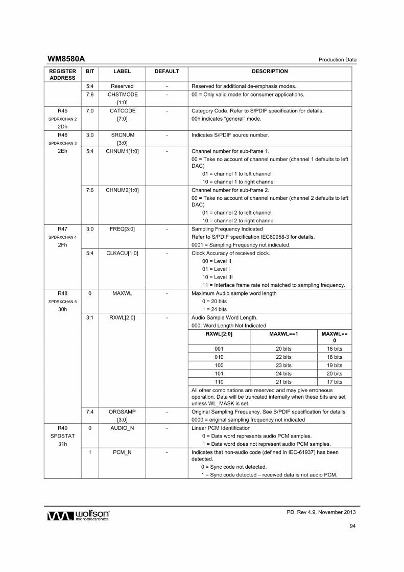
WM8580A Production Data
w PD, Rev 4.9, November 2013
94
REGISTER ADDRESS
BIT LABEL DEFAULT DESCRIPTION
5:4 Reserved - Reserved for additional de-emphasis modes.
7:6 CHSTMODE
[1:0]
- 00 = Only valid mode for consumer applications.
R45
SPDRXCHAN 2
2Dh
7:0 CATCODE
[7:0]
- Category Code. Refer to S/PDIF specification for details.
00h indicates “general” mode.
R46
SPDRXCHAN 3
2Eh
3:0 SRCNUM
[3:0]
- Indicates S/PDIF source number.
5:4 CHNUM1[1:0] - Channel number for sub-frame 1.
00 = Take no account of channel number (channel 1 defaults to left DAC)
01 = channel 1 to left channel
10 = channel 1 to right channel
7:6 CHNUM2[1:0] Channel number for sub-frame 2.
00 = Take no account of channel number (channel 2 defaults to left DAC)
01 = channel 2 to left channel
10 = channel 2 to right channel
R47
SPDRXCHAN 4
2Fh
3:0 FREQ[3:0] - Sampling Frequency Indicated
Refer to S/PDIF specification IEC60958-3 for details.
0001 = Sampling Frequency not indicated.
5:4 CLKACU[1:0] - Clock Accuracy of received clock.
00 = Level II
01 = Level I
10 = Level III
11 = Interface frame rate not matched to sampling frequency.
R48
SPDRXCHAN 5
30h
0 MAXWL - Maximum Audio sample word length
0 = 20 bits
1 = 24 bits
3:1 RXWL[2:0] - Audio Sample Word Length.
000: Word Length Not Indicated
RXWL[2:0] MAXWL==1 MAXWL==0
001 20 bits 16 bits
010 22 bits 18 bits
100 23 bits 19 bits
101 24 bits 20 bits
110 21 bits 17 bits
All other combinations are reserved and may give erroneous operation. Data will be truncated internally when these bits are set unless WL_MASK is set.
7:4 ORGSAMP
[3:0]
- Original Sampling Frequency. See S/PDIF specification for details.
0000 = original sampling frequency not indicated
R49
SPDSTAT
31h
0 AUDIO_N - Linear PCM Identification
0 = Data word represents audio PCM samples.
1 = Data word does not represent audio PCM samples.
1 PCM_N - Indicates that non-audio code (defined in IEC-61937) has been detected.
0 = Sync code not detected.
1 = Sync code detected – received data is not audio PCM.
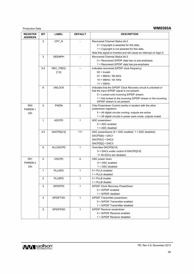
Production Data WM8580A
w PD, Rev 4.9, November 2013
95
REGISTER ADDRESS
BIT LABEL DEFAULT DESCRIPTION
2 CPY_N - Recovered Channel Status bit-2.
0 = Copyright is asserted for this data.
1 = Copyright is not asserted for this data.
Note this signal is inverted and will cause an interrupt on logic 0.
3 DEEMPH - Recovered Channel Status bit-3
0 = Recovered S/PDIF data has no pre-emphasis.
1 = Recovered S/PDIF data has pre-emphasis
5:4 REC_FREQ
[1:0]
-- Indicates recovered S/PDIF clock frequency:
00 = Invalid
01 = 96kHz / 88.2kHz
10 = 48kHz / 44.1kHz
11 = 32kHz
6 UNLOCK - Indicates that the S/PDIF Clock Recovery circuit is unlocked or that the input S/PDIF signal is not present.
0 = Locked onto incoming S/PDIF stream.
1 = Not locked to the incoming S/PDIF stream or the incoming S/PDIF stream is not present.
R50
PWRDN 1
32h
0 PWDN 0 Chip Powerdown Control (works in tandem with the other powerdown registers):
0 = All digital circuits running, outputs are active
1 = All digital circuits in power save mode, outputs muted
1 ADCPD 1 ADC powerdown:
0 = ADC enabled
1 = ADC disabled
4:2 DACPD[2:0] 111 DAC powerdowns (0 = DAC enabled, 1 = DAC disabled)
DACPD[0] = DAC1
DACPD[1] = DAC2
DACPD[2] = DAC3
6 ALLDACPD 1 Overrides DACPD[3:0]
0 = DACs under control of DACPD[3:0]
1= All DACs are disabled.
R51
PWRDN 2
33h
0 OSCPD 0 OSC power down
0 = OSC enabled
1 = OSC disabled
1 PLLAPD 1 0 = PLLA enabled
1 = PLLA disabled
2 PLLBPD 1 0 = PLLB enable
1 = PLLB disable
3 SPDIFPD 1 S/PDIF Clock Recovery PowerDown
0 = S/PDIF enabled
1 = S/PDIF disabled
4 SPDIFTXD 1 S/PDIF Transmitter powerdown
0 = S/PDIF Transmitter enabled
1 = S/PDIF Transmitter disabled
5 SPDIFRXD 1 S/PDIF Receiver powerdown
0 = S/PDIF Receiver enabled
1 = S/PDIF Receiver disabled
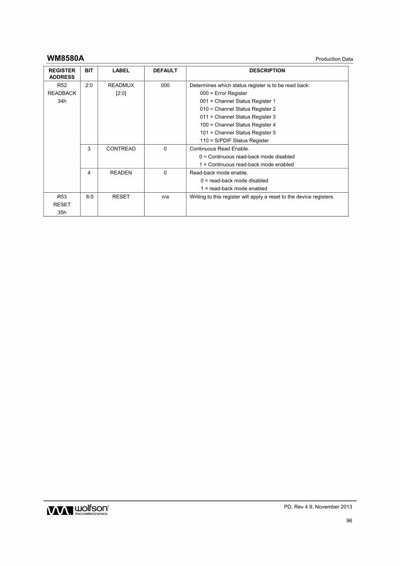
WM8580A Production Data
w PD, Rev 4.9, November 2013
96
REGISTER ADDRESS
BIT LABEL DEFAULT DESCRIPTION
R52
READBACK
34h
2:0 READMUX
[2:0]
000 Determines which status register is to be read back:
000 = Error Register
001 = Channel Status Register 1
010 = Channel Status Register 2
011 = Channel Status Register 3
100 = Channel Status Register 4
101 = Channel Status Register 5
110 = S/PDIF Status Register
3 CONTREAD 0 Continuous Read Enable.
0 = Continuous read-back mode disabled
1 = Continuous read-back mode enabled
4 READEN 0 Read-back mode enable.
0 = read-back mode disabled
1 = read-back mode enabled
R53
RESET
35h
8:0 RESET n/a Writing to this register will apply a reset to the device registers.
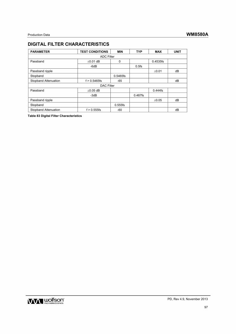
Production Data WM8580A
w PD, Rev 4.9, November 2013
97
DIGITAL FILTER CHARACTERISTICS
PARAMETER TEST CONDITIONS MIN TYP MAX UNIT
ADC Filter
Passband 0.01 dB 0 0.4535fs
-6dB 0.5fs
Passband ripple 0.01 dB
Stopband 0.5465fs
Stopband Attenuation f > 0.5465fs -65 dB
DAC Filter
Passband 0.05 dB 0.444fs
-3dB 0.487fs
Passband ripple 0.05 dB
Stopband 0.555fs
Stopband Attenuation f > 0.555fs -60 dB
Table 83 Digital Filter Characteristics
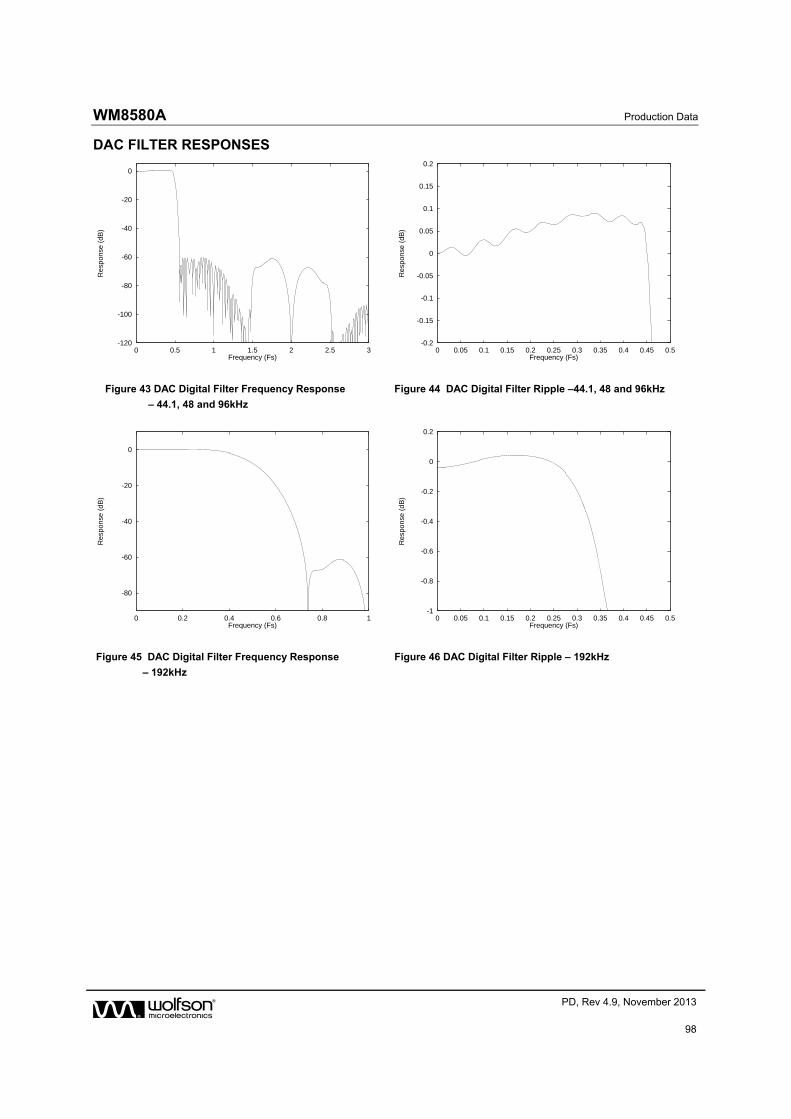
WM8580A Production Data
w PD, Rev 4.9, November 2013
98
DAC FILTER RESPONSES
-120
-100
-80
-60
-40
-20
0
0 0.5 1 1.5 2 2.5 3
Res
pons
e (d
B)
Frequency (Fs)
-0.2
-0.15
-0.1
-0.05
0
0.05
0.1
0.15
0.2
0 0.05 0.1 0.15 0.2 0.25 0.3 0.35 0.4 0.45 0.5
Res
pons
e (d
B)
Frequency (Fs)
Figure 43 DAC Digital Filter Frequency Response
– 44.1, 48 and 96kHz
Figure 44 DAC Digital Filter Ripple –44.1, 48 and 96kHz
-80
-60
-40
-20
0
0 0.2 0.4 0.6 0.8 1
Res
pons
e (d
B)
Frequency (Fs)
-1
-0.8
-0.6
-0.4
-0.2
0
0.2
0 0.05 0.1 0.15 0.2 0.25 0.3 0.35 0.4 0.45 0.5
Res
pons
e (d
B)
Frequency (Fs)
Figure 45 DAC Digital Filter Frequency Response
– 192kHz
Figure 46 DAC Digital Filter Ripple – 192kHz
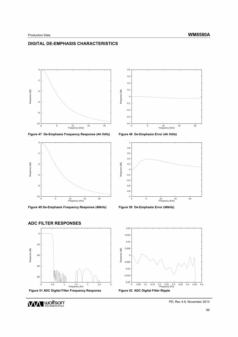
Production Data WM8580A
w PD, Rev 4.9, November 2013
99
DIGITAL DE-EMPHASIS CHARACTERISTICS
-10
-8
-6
-4
-2
0
0 5 10 15 20
Res
pons
e (d
B)
Frequency (kHz)
-0.4
-0.3
-0.2
-0.1
0
0.1
0.2
0.3
0.4
0 5 10 15 20
Res
pons
e (d
B)
Frequency (kHz)
Figure 47 De-Emphasis Frequency Response (44.1kHz) Figure 48 De-Emphasis Error (44.1kHz)
-10
-8
-6
-4
-2
0
0 5 10 15 20
Res
pons
e (d
B)
Frequency (kHz)
-1
-0.8
-0.6
-0.4
-0.2
0
0.2
0.4
0.6
0.8
1
0 5 10 15 20
Res
pons
e (d
B)
Frequency (kHz)
Figure 49 De-Emphasis Frequency Response (48kHz) Figure 50 De-Emphasis Error (48kHz)
ADC FILTER RESPONSES
-80
-60
-40
-20
0
0 0.5 1 1.5 2 2.5 3
Res
pons
e (d
B)
Frequency (Fs)
-0.02
-0.015
-0.01
-0.005
0
0.005
0.01
0.015
0.02
0 0.05 0.1 0.15 0.2 0.25 0.3 0.35 0.4 0.45 0.5
Res
pons
e (d
B)
Frequency (Fs)
Figure 51 ADC Digital Filter Frequency Response Figure 52 ADC Digital Filter Ripple
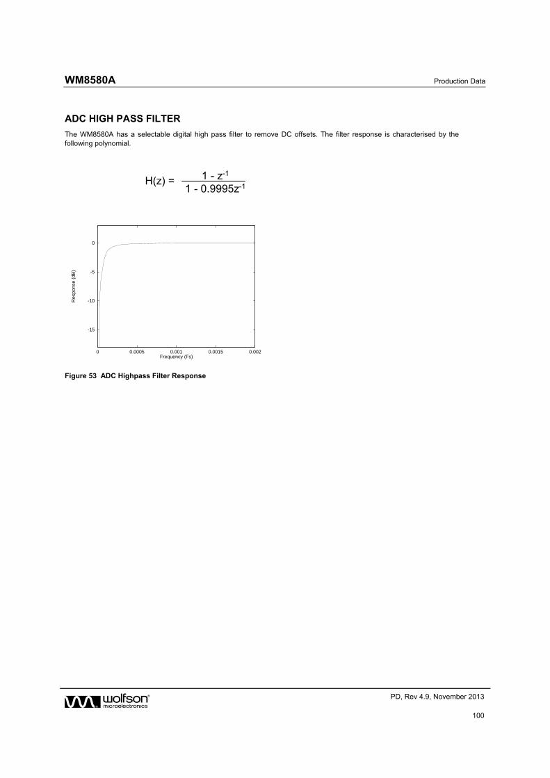
WM8580A Production Data
w PD, Rev 4.9, November 2013
100
ADC HIGH PASS FILTER
The WM8580A has a selectable digital high pass filter to remove DC offsets. The filter response is characterised by the following polynomial.
Figure 53 ADC Highpass Filter Response
1 - z-1
1 - 0.9995z-1H(z) =
-15
-10
-5
0
0 0.0005 0.001 0.0015 0.002
Res
pons
e (d
B)
Frequency (Fs)
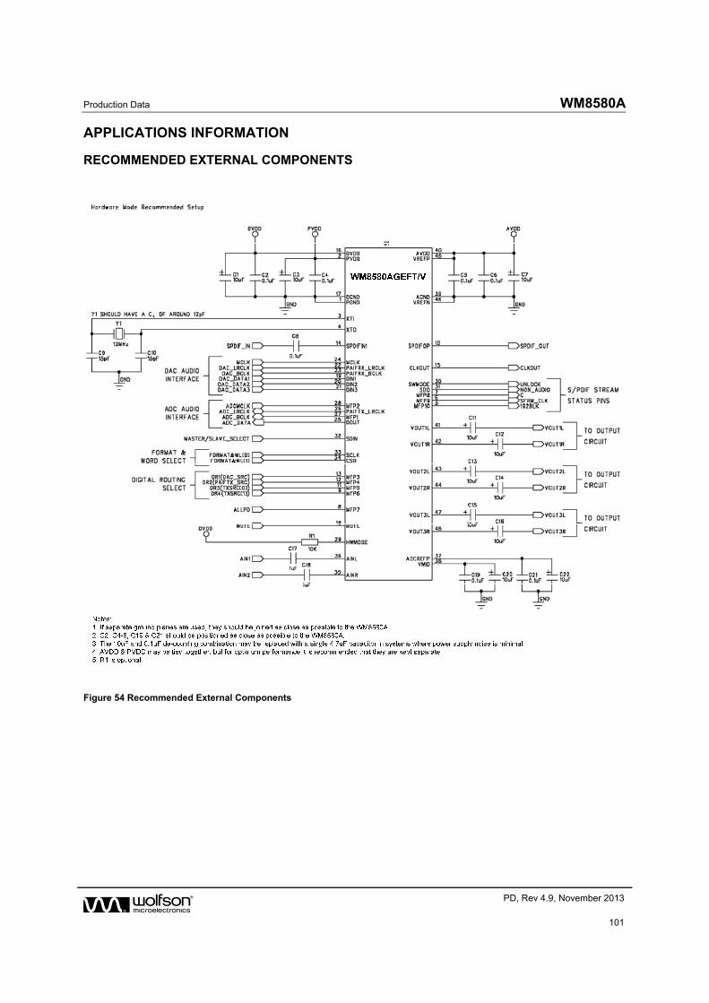
Production Data WM8580A
w PD, Rev 4.9, November 2013
101
APPLICATIONS INFORMATION
RECOMMENDED EXTERNAL COMPONENTS
Figure 54 Recommended External Components
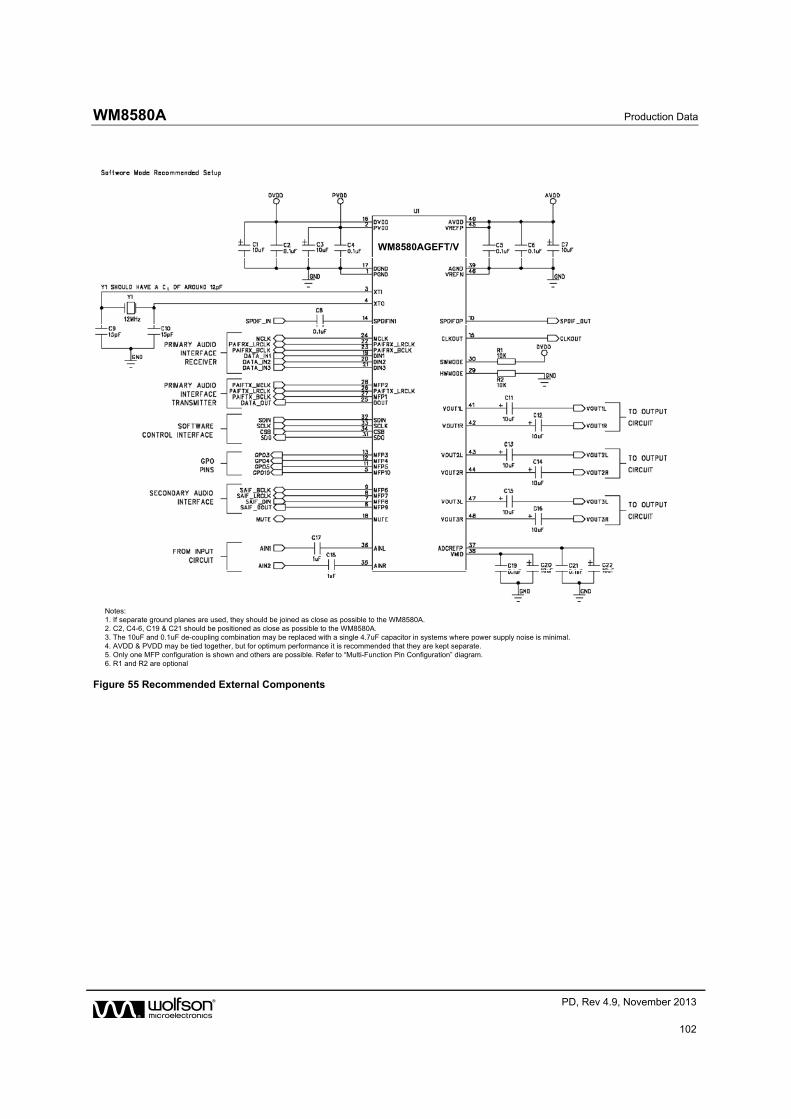
WM8580A Production Data
w PD, Rev 4.9, November 2013
102
WM8580AGEFT/V
Notes:1. If separate ground planes are used, they should be joined as close as possible to the WM8580A.2. C2, C4-6, C19 & C21 should be positioned as close as possible to the WM8580A.3. The 10uF and 0.1uF de-coupling combination may be replaced with a single 4.7uF capacitor in systems where power supply noise is minimal.4. AVDD & PVDD may be tied together, but for optimum performance it is recommended that they are kept separate.5. Only one MFP configuration is shown and others are possible. Refer to “Multi-Function Pin Configuration” diagram.6. R1 and R2 are optional
Figure 55 Recommended External Components
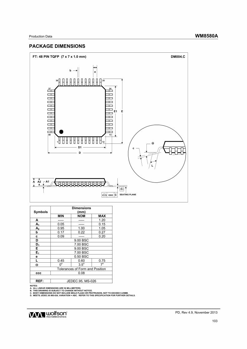
Production Data WM8580A
w PD, Rev 4.9, November 2013
103
PACKAGE DIMENSIONS
NOTES:A. ALL LINEAR DIMENSIONS ARE IN MILLIMETERS.B. THIS DRAWING IS SUBJECT TO CHANGE WITHOUT NOTICE.C. BODY DIMENSIONS DO NOT INCLUDE MOLD FLASH OR PROTRUSION, NOT TO EXCEED 0.25MM.D. MEETS JEDEC.95 MS-026, VARIATION = ABC. REFER TO THIS SPECIFICATION FOR FURTHER DETAILS.
DM004.CFT: 48 PIN TQFP (7 x 7 x 1.0 mm)
SymbolsDimensions
(mm)MIN NOM MAX
A ----- ----- 1.20A1 0.05 ----- 0.15A2 0.95 1.00 1.05b 0.17 0.22 0.27c 0.09 ----- 0.20D 9.00 BSCD1 7.00 BSCE 9.00 BSCE1 7.00 BSCe 0.50 BSCL 0.45 0.60 0.75 0o 3.5o 7o
Tolerances of Form and Positionccc 0.08
REF: JEDEC.95, MS-026
2536
eb
121
D1
D
E1 E
13
2437
48
A A2 A1
SEATING PLANEccc C
-C-
c
L
WM8580A Production Data
w PD, Rev 4.9, November 2013
104
IMPORTANT NOTICE
Wolfson Microelectronics plc (“Wolfson”) products and services are sold subject to Wolfson’s terms and conditions of sale, delivery and payment supplied at the time of order acknowledgement.
Wolfson warrants performance of its products to the specifications in effect at the date of shipment. Wolfson reserves the right to make changes to its products and specifications or to discontinue any product or service without notice. Customers should therefore obtain the latest version of relevant information from Wolfson to verify that the information is current.
Testing and other quality control techniques are utilised to the extent Wolfson deems necessary to support its warranty. Specific testing of all parameters of each device is not necessarily performed unless required by law or regulation.
In order to minimise risks associated with customer applications, the customer must use adequate design and operating safeguards to minimise inherent or procedural hazards. Wolfson is not liable for applications assistance or customer product design. The customer is solely responsible for its selection and use of Wolfson products. Wolfson is not liable for such selection or use nor for use of any circuitry other than circuitry entirely embodied in a Wolfson product.
Wolfson’s products are not intended for use in life support systems, appliances, nuclear systems or systems where malfunction can reasonably be expected to result in personal injury, death or severe property or environmental damage. Any use of products by the customer for such purposes is at the customer’s own risk.
Wolfson does not grant any licence (express or implied) under any patent right, copyright, mask work right or other intellectual property right of Wolfson covering or relating to any combination, machine, or process in which its products or services might be or are used. Any provision or publication of any third party’s products or services does not constitute Wolfson’s approval, licence, warranty or endorsement thereof. Any third party trade marks contained in this document belong to the respective third party owner.
Reproduction of information from Wolfson datasheets is permissible only if reproduction is without alteration and is accompanied by all associated copyright, proprietary and other notices (including this notice) and conditions. Wolfson is not liable for any unauthorised alteration of such information or for any reliance placed thereon.
Any representations made, warranties given, and/or liabilities accepted by any person which differ from those contained in this datasheet or in Wolfson’s standard terms and conditions of sale, delivery and payment are made, given and/or accepted at that person’s own risk. Wolfson is not liable for any such representations, warranties or liabilities or for any reliance placed thereon by any person.
The product described in this datasheet incorporates clocking technology that has been licensed from Sonopsis Ltd. which is protected by patents including EP1611684B1 and US7495515. Additional patent applications are pending.
ADDRESS:
Wolfson Microelectronics plc
Westfield House
26 Westfield Road
Edinburgh
EH11 2QB
United Kingdom
Tel :: +44 (0)131 272 7000
Fax :: +44 (0)131 272 7001
Email :: [email protected]
Production Data WM8580A
w PD, Rev 4.9, November 2013
105
REVISION HISTORY
DATE REV DESCRIPTION OF CHANGES CHANGED BY
04/06/13 4.8 Updated to show part as WM8580A throughout the datasheet. JMacD
23/10/13 4.9 Recommended External Component Diagrams: Note 4 corrected (DVDD changed to AVDD)
JMacD