multi-physics modeling
TRANSCRIPT

University of Tennessee, Knoxville University of Tennessee, Knoxville
TRACE: Tennessee Research and Creative TRACE: Tennessee Research and Creative
Exchange Exchange
Doctoral Dissertations Graduate School
8-2016
MULTI-PHYSICS MODELING MULTI-PHYSICS MODELING
Ahmadreza Ghahremani University of Tennessee, Knoxville, [email protected]
Follow this and additional works at: https://trace.tennessee.edu/utk_graddiss
Part of the Electromagnetics and Photonics Commons, Electronic Devices and Semiconductor
Manufacturing Commons, and the Other Electrical and Computer Engineering Commons
Recommended Citation Recommended Citation Ghahremani, Ahmadreza, "MULTI-PHYSICS MODELING. " PhD diss., University of Tennessee, 2016. https://trace.tennessee.edu/utk_graddiss/3915
This Dissertation is brought to you for free and open access by the Graduate School at TRACE: Tennessee Research and Creative Exchange. It has been accepted for inclusion in Doctoral Dissertations by an authorized administrator of TRACE: Tennessee Research and Creative Exchange. For more information, please contact [email protected].

To the Graduate Council:
I am submitting herewith a dissertation written by Ahmadreza Ghahremani entitled "MULTI-
PHYSICS MODELING." I have examined the final electronic copy of this dissertation for form and
content and recommend that it be accepted in partial fulfillment of the requirements for the
degree of Doctor of Philosophy, with a major in Electrical Engineering.
Aly E. Fathy, Major Professor
We have read this dissertation and recommend its acceptance:
Syed K. Islam, Gong Gu, Thomas T. Meek
Accepted for the Council:
Carolyn R. Hodges
Vice Provost and Dean of the Graduate School
(Original signatures are on file with official student records.)
A Dissertation Presented for the
Doctor of Philosophy
Degree
The University of Tennessee, Knoxville
Ahmadreza Ghahremani
August 2016
MULTI-PHYSICS MODELING

ii
Dedication
I dedicate this dissertation to my dear wife Melika Roknsharifi and my dear parents Fatima Sarmadi
and Mahmoud Ghahremani, who supported me all time in my life, and also two of my great advisors, Dr.
Aly E. Fathy, and Dr. Mohammad Sadegh Abrishamian.

iii
Acknowledgment
This work was supported by the grant from the National Science Foundation of USA (Grant No. NSF
EPS- 1004083).
It is a pleasure to thank those who helped me to make this dissertation possible. First of all, I owe my
deepest gratitude to my great advisor Dr. Aly E. Fathy, whose encouragement, guidance and support
helped me a lot.
I also would like to thank my committee members Dr. Syed K. Islam, Dr. Gong GU, and Dr. Thomas
T. Meek who tremendously helped me to improve the quality of this work.
I want to thank my dear parents Fatima Sarmadi, Mahmoud Ghahremani, and my dear wife Melika
Roknsharifi, for all support and encouragements in my whole life.

iv
Having access to powerful processors allows scientists to carry out aggressive numerical computations
to bridge the gaps which already exist among different fields of physics by exploring new multi-physics
models to approach real life models of various phenomena happening around us in real life and accounting
of the various coupling and dependence between the various physical parameters and material parameters.
Scientists greatly appreciate multi-physics modeling as they recognize:
1- Prototyping is expensive
2- Most of available CAD tools are not addressing the real model or accounting between the different
parameters in physics.
3- Some difficulties to optimize the real model without simulation (due to a wide range of parameters)
4- Even some measurements are complicated and require expensive set-up for full evaluation and
trouble shooting. Some parameters are even non-measurable.
Solving multi-physics problems is always a complicated process. For instance, access to a reliable
database to initialize data or to set boundary conditions is an important issue, but it may take long time
(several years) to extract data from measurements. Nowadays, there is a big competition among developers
of commercial CAD tools to provide specific features or capabilities (as a multi-physics solver).
Fortunately, by developing powerful CAD tools, some complex questions will be answered, and also it may
turn out to achieve some exciting innovations. In this study, two relevant electrical engineering problems
(improving solar cells’ efficiency and effect of heat on electronic circuits like processors) will be
investigated. The first one is analysis of solar cells, and the second one is speed deterioration of
microprocessors due to generated heat. Both problems require to do some multi-physics modeling, and it
requires investigating different set of parameters in physics. Solar cell’s operation includes optics,
Abstract

v
semiconductor physics, and electronics. Modeling a solar cell could turn out to achieve higher efficiency.
Similarly, solving a microprocessor’s problems include heat analysis, and mechanical stress analysis.
Modeling microprocessors can lead to better heat sinks or cooling system and could achieve to sustained
speeds and performance.

vi
Table of Contents
CHAPTER 1 Solar Cells Multi-Physics Modeling ...................................................................................... 1
1.1. Background-solar cells ....................................................................................................................... 1
1.2. Theories.............................................................................................................................................. 6
1.2.1. Solving solar cell problem in 3D ................................................................................................ 6
1.2.2. Initialization of the simulator .................................................................................................... 10
1.2.3. Electrical outputs....................................................................................................................... 12
1.3. Simulated and measured results-no plasmon ................................................................................... 12
1.4. Electromagnetic field analysis of MNPs .......................................................................................... 18
1.5. Simulated and measured results-with plasmon ................................................................................ 19
1.6. Conclusion ....................................................................................................................................... 23
CHAPTER 2 Strategies for Designing Highly Efficient Thin Film Amorphous Silicon Solar Cells ......... 24
2.1. Introduction ...................................................................................................................................... 24
2.2. Simulation analysis .......................................................................................................................... 26
2.3. Impact defects .................................................................................................................................. 27
2.4. Optimization of highly doped regions ............................................................................................. 33
2.5. Conclusion ....................................................................................................................................... 33
2.6. Appendix theories ............................................................................................................................ 34
CHAPTER 3 Electro Thermal Design Issues-Literature Review .............................................................. 41
3.1. Introduction ...................................................................................................................................... 41
3.1.1. History of electro thermal problems in electronic devices ........................................................ 42
3.1.2. Basic failures mechanisms due to high temperature ................................................................. 46
CHAPTER 4 Modeling Electro Thermal Problems ................................................................................... 52
4.1. Background ...................................................................................................................................... 52
4.1.1. Joule-heating modeling inside IC package ............................................................................... 53
4.1.2. Joule-heating outside IC package ............................................................................................. 55
4.2. Basic analysis of electro-thermal problems ..................................................................................... 56
4.2.1. Model development................................................................................................................... 57
4.3. Electro-thermal simulation for devices at low frequency ................................................................ 59
4.3.1. Analysis of 3D electro-thermal simulations-3D integration system ......................................... 59
4.3.2. Modeling of 3D electro-thermal -3D daisy chain ..................................................................... 70

vii
4.4. Analysis of 3D electro-thermal simulation for devices at high frequencies .................................... 76
4.4.1. Analysis of 3D electro-thermal simulations- GaN device power amplifier .............................. 76
4.5. Conclusion ....................................................................................................................................... 90
CHAPTER 5 Thermal Measurements ........................................................................................................ 92
5.1. RF power amplifier .......................................................................................................................... 92
5.2. Modeling of the amplifier ................................................................................................................ 93
5.3. Measurement and simulation ........................................................................................................... 93
5.4. Conclusion ..................................................................................................................................... 101
CHAPTER 6 Contributions and Future Work ......................................................................................... 102
6.1. Introduction .................................................................................................................................... 102
6.2. Contributions.................................................................................................................................. 103
6.3. Future work in modeling solar cells ............................................................................................... 105
6.4. Future work in modeling electro-thermal problem ........................................................................ 106
References ................................................................................................................................................. 107
Appendix ................................................................................................................................................... 117
Vita ............................................................................................................................................................ 125

viii
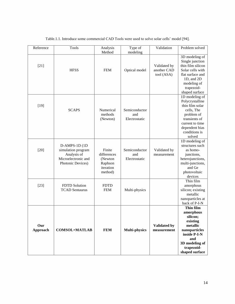
List of Tables Table.1.1. Introduce some commercial CAD Tools were used to solve solar cells’ model [94].. ............................ 14
Table.1.2. the utilized value of each parameter for the utilized validation example.. ............................................ 15
Table. 2.1 The utilized value of each parameter. ............................................................................................... 40
Table.3.1 (a). Failure classifications and mechanisms are listed (after [69])... ...................................................... 50
Table.3.1 (b). Failure classifications and mechanisms are listed (after [69])... ..................................................... 51
Table.4.1. Evolution of for Intel® commercial processors features. .................................................................... 54
Table.4.2 power consumption of the stacked chips [65] at 6 different regions indicated in Fig. 4.3........................ 59
Table.4.3 the thickness of layers and thermal conductivity of the materials [65]. ................................................. 61
Table.4.4 (a) electro-thermal properties of copper. ............................................................................................ 61
Table.4.4 (b) electro-thermal properties of underfill. ......................................................................................... 61
Table.4.4 (c) electro-thermal properties of glass-ceramic. .................................................................................. 62
Table.4.4 (d) electro-thermal properties of C4. ................................................................................................. 62
Table.4.4 (e) electro-thermal properties of Chip. ............................................................................................... 62
Table.4.4 (f) electro-thermal properties of TIM. ............................................................................................... 62
Table.4.4 (g) electro-thermal properties of TSV. ............................................................................................... 62
Table.4.5. Comparison between our simulation results with measured and calculated data from [66]. ................... 74
Table.4.6 (a) electro-thermal properties of copper. ............................................................................................ 78
Table.4.6 (b) electro-thermal properties of FR4. ............................................................................................... 78
Table.4.6 (c) electro-thermal properties of Solder, 60Sn-40Pb. .......................................................................... 78
Table.4.6 (d) electro-thermal properties of GaN. ............................................................................................... 78
Table.4.6 (e) electro-thermal properties of Solder, VIA. .................................................................................... 79
Table.4.6 (f) electro-thermal properties of Rogers. ............................................................................................ 79
Table.4.6 (g) electro-thermal properties of TIM. ............................................................................................... 79
Table.5.1. RF power amplifier specifications. ................................................................................................... 93
Table.5.2 (a) electro-thermal properties of Aluminum. ............................................................................................... 99
Table.5.2 (b) electro-thermal properties of Copper. .................................................................................................... 95
Table.5.2 (c) electro-thermal properties of FR4. ......................................................................................................... 95
Table.5.2 (d) electro-thermal properties of Silica Glass. ............................................................................................. 95
Table.5.2 (e) electro-thermal properties of Solder 60Sn-40Pb. ................................................................................... 95

ix
List of Figures Fig.1.1. Efficiency versus cost for all solar cells (Green represents first generation; Yellow represents second
generation; Red represents third generation) [5]. ................................................................................................. 3
Fig.1.2. Photon intensity in a 3D cell [94]. ......................................................................................................... 6
Fig.1.3. Tetrahedral Mesh Generation of the 3D device for one unit cell [94]. ....................................................... 9
Fig.1.4. (a) Standard solar spectrum generated with the BRITE Monte Carlo Solar Insolation Model using the
atmospheric conditions specified in [41]; (b) the utilized update of the spectral irradiance—downloaded from [42].
.................................................................................................................................................................... 11
Fig.1.5 (a) Schematic of the P-I-N device; (b) EQE curve (comparison between measurement [14], and simulation
result) [94]. ................................................................................................................................................... 16
Fig.1.6. J-V curve (simulation), and a comparison between simulation and measured data [14] is shown in the
embedded Table [94]...................................................................................................................................... 17
Fig.1.7. Simulation results for solar cells without MNPs; the blue solid line represents reflection coefficient; and red
dash line shows the absorbance coefficient vs. wavelength [94]. ........................................................................ 17
Fig.1.8. Extinction coefficient of amorphous silicon [94]................................................................................... 18
Fig.1.9. Normalized monostatic radar cross section for a conducting sphere as a function of sphere radius [47]. .... 19
Fig.1.10. Normalized monostatic RCS for a single silver nanoparticle (radius=10nm) inside vacuum; solid blue line
represents simulation result and red dash line shows the analytical method [94]. ................................................. 20
Fig.1.11. (a) Schematic of a PIN device; (b) EQE curve using MNPs embedded inside SnO:F.; blue dash line
represents measurement [14]; orange solid line shows simulation [94]. .............................................................. 21
Fig.1.12. (a) A comparison between the measurements of [14] and simulation data for the electrical outputs; (b)
Simulation results for the Reflection coefficient; solid blue line represents reflection from the solar cell without
MNPs; dash black line shows reflection from the solar cell with MNPs embedded inside the TCO layer on top of the
PIN device [94]. ............................................................................................................................................ 21
Fig.1.13. (a) schematic of MNPs are shown as blue spheres embedded inside TCO (b) the intensity of power flow of
the light (wavelength@720 nm) [94]. .............................................................................................................. 22
Fig.2.1. Paths of light inside solar cells for different type of electrodes [95]. ....................................................... 25
Fig.2.2. (a) Schematic of the PIN device; (b) EQE curve (dash line represents measurement [11]; solid line
represents simulation result) [95]..................................................................................................................... 29
Fig.2.3. (a) TEM cross-section [11], and Schematic of the PIN device; (b) EQE curve (dash line represents
measurement [11]; solid line represents simulation result), after considering of defects [95]. ................................ 30
Fig.2.4. (a) Schematic of the PIN device; (b) Comparison of EQE with and without MNPs; solid line represents [95].
.................................................................................................................................................................... 31
Fig.2.5. (a) Schematic of the PIN device; (b) Using different size of MNPs, in two different locations EQE curve for
the simulation (solid line represents after optimization-black; dash line represents No MNPs blue) [95]. ............... 32
Fig.2.6. 3D schematic of the solar cell; presents the excitation and the boundary conditions in optics [95]. ............ 36
Fig. 3.1. Moore’s law [70]. ............................................................................................................................. 41
Fig.3.2. Heat flux generated for different types of microprocessors since 1959 [72]. ............................................ 42

x
Fig.3.3.Cooling system was designed for the 3081 computer [73]. ..................................................................... 43
Fig.3.4. Improvement in water-cooling systems for IBM processors [73]. ........................................................... 43
Fig.3.5. Water-cooling machine for the Mac G5 computer [73]. ......................................................................... 44
Fig.3.6. Using microfluidic channels in microprocessors to transfer the heat [91]. ............................................... 45
Fig. 3.7. Using TIM layer and a Fan to cool down INTEL processors. ................................................................ 45
Fig.3.8. Main causes of failures in electronic packages [76]. .............................................................................. 46
Fig. 3.9. a) A SEM image of a Bump cross section; b) magnification of a damage in a Bump [67]. ....................... 48
Fig.3.10. Current density of bump vs size of bump [69]. ................................................................................... 48
Fig.3.11. Cracks created by heat as a basic package failure. ............................................................................... 48
Fig.3.12. Flip-chip package with copper heat sink [89]. ..................................................................................... 49
Fig.3.13. Single copper pillar system supported by a polymer [90]. .................................................................... 49
Fig.3.14. Flip chip ball grid array (a) Front; (b) back side; (c) SEM of copper pillar bumps. (d) Magnified copper
pillar bumps [85]. .......................................................................................................................................... 49
Fig.4.1. Evolution of power density for Intel processors [55].4.4.1. Analysis of 3D Electro-thermal
Simulations- GaN device power amplifier .................................................................................................. 55
Fig.4.2. Electric power map for the stacked chips (a) CPU (b) RAM [65].. ......................................................... 59
Fig.4.3. 3D integrated system, stacked chips, Chip power map and TSVs for CPU and Memory [65]. ................... 60
Fig.4.4. Mesh cells for 3D integrated package. ................................................................................................. 64
Fig.4.5. Electro-thermal boundary conditions for the package. ........................................................................... 64
Fig.4.6. Temperature distribution of the 3D Chip before and after joule heating. ................................................. 65
Fig.4.7. Final temperature distribution of CPU1 from Ref. [65].5.3. Measurement and Simulation ................... 65
Fig.4.8. IR-Drop in 3D stacked chip after using joule-heating. ........................................................................... 66
Fig.4.9. Thermal TSVs and parallel copper power plates. .................................................................................. 67
Fig.4.10.IR-Drop map before and after adding copper plates ............................................................................. 68
Fig.4.11. Thermal map before expanding thermal TSVs. ................................................................................... 69
Fig.4.12. Thermal map after expanding thermal TSVs. ...................................................................................... 69
Fig.4.13. (a) Test vehicle and layout for temperature and resistance measurements; (b) Layout of circuits an bumps
on flip-chip test vehicle; (c) Configuration of electrified daisy chain. [66] .......................................................... 71
Fig.4.14. 3D daisy chain located in the silicon. ................................................................................................. 72
Fig.4.15.The current flow 3D daisy chain located in the silicon. ......................................................................... 73
Fig.4.16. SEM image of Bump; cross sectioning, Magnification of damage in bump [67]. ................................... 73
Fig.4.17. New structure of a chain and the current distribution.. ......................................................................... 75
Fig.4.18. Structure of a three-stage power amplifier. ......................................................................................... 77

xi
Fig.4.19. Structure of a three stage power amplifier- color code: orange: heatsink; green: TIM; red: GaN device;
yellow: RF transmission lines; blue: DC PCB board; gray: air . ........................................................................ 77
Fig.4.20. Mesh cells for the GaN device power amplifier.. ................................................................................ 79
Fig.4.21. Heat source boundary condition for the power amplifier.. .................................................................... 80
Fig.4.22. Thermal distribution on the surface and inside the RF power amplifier when the thickness of TIM layer is
1 mil and the thermal conductivity is 12.9[W/(m*K)]........................................................................................ 82
Fig.4.23. Thermal distribution on the surface and inside the RF power amplifier when the thickness of TIM layer is
1 mil and the thermal conductivity is 8 [W/(m*K)].. ......................................................................................... 83
Fig.4.24. Thermal distribution on the surface and inside the RF power amplifier when the thickness of TIM layer is
1 mil and the thermal conductivity is 3 [W/(m*K)].. ......................................................................................... 84
Fig.4.25. Thermal distribution on the surface and inside the RF power amplifier when the thickness of TIM layer is
1 mil and the thermal conductivity is 1 [W/(m*K)].. ......................................................................................... 85
Fig.4.26. Thermal distribution on the surface and inside the RF power amplifier when the thickness of TIM layer is
3 mil and the thermal conductivity is 12.9 [W/(m*K)].. ..................................................................................... 86
Fig.4.27. Thermal distribution on the surface and inside the RF power amplifier when the thickness of TIM layer is
1 mil and the thermal conductivity is 12.9 [W/(m*K)].. ..................................................................................... 87
Fig.4.28. Thermal distribution on the surface and inside the RF power amplifier when the thickness of TIM layer is
1 mil and the thermal conductivity is 12.9 [W/(m*K)], and heatsink is made of Copper.. ..................................... 88
Fig.4.29. Thermal distribution on the surface and inside the RF power amplifier when the thickness of TIM layer is
1 mil and the thermal conductivity is 12.9 [W/(m*K)], and heatsink made of Aluminum.. ................................... 89
Fig.5.1. 70cm PCB board of the linear amplifier kit 7W.. .................................................................................. 92
Fig.5.2. Prototyped version and the generated model in COMSOL. .................................................................... 94
Fig.5.3. 3D model of the structure built in COMSOL. ....................................................................................... 94
Fig.5.4. Electric and thermal boundary conditions. ........................................................................................... 96
Fig.5.5. Mesh Generation of the whole structure in COMSOL.. ......................................................................... 96
Fig.5.6. The setup test for measuring the thermal distribution on the surface of the power amplifier by FLIR camera..
.................................................................................................................................................................... 97
Fig.5.7. Simulation result for the thermal distribution inside and on the surfaces of the PCB board (Fan is off).. .... 98
Fig.5.8. Thermal image is taken by FLIR camera from the power amplifier (the fan is off) .................................. 98
Fig.5.9. The CPU fan has been used for the experiment. .................................................................................... 99
Fig.5.10. Simulated thermal distribution when the fan is on with air speed = 0.5 m/s. .......................................... 99
Fig.5.11. Simulated thermal distribution when fan is on with air speed = 5 m/s ................................................... 99
Fig.5.12. Comparing the thermal image from FLIR camera and simulated data (Fan is on, with air speed 5m/s). . 100
Fig. A1 3D structure of a processor designed in COMSOL.. ........................................................................... 118
Fig. A2 3D structure of a processor designed in COMSOL with material library. ............................................. 119
Fig. A3 set parameters under definitions . ..................................................................................................... 119

xii
Fig. A4 Mesh cells of 3D processors generated by COMSOL . ....................................................................... 120
Fig. A5 Joule heating regions selected in COMSOL........................................................................................ 120
Fig. A6 Boundary conditions set in COMSOL.. .............................................................................................. 121
Fig. A7 setting heat source.. .......................................................................................................................... 121
1
CHAPTER 1
Solar Cells Multi-Physics Modeling
1.1. Background-solar cells
Solar energy is an attractive source of energy because of its abundance on our planet. For sure, harvesting
the solar energy via inexpensive and efficient technology is an important challenge of the world. In a solar
cell, light (photons) is absorbed and converted to electron-hole pairs (generation), which must be separated
in order to create electricity; otherwise it could recombine (recombination), or it could be absorbed into
heat (ohmic loss). A good design should provide the mechanism of improving generation, minimizing
recombination, and reducing propagation loss.
The development of solar cells has gone already into three generations. The first generation of
photovoltaics is single P-N junction or polycrystalline silicon solar cells. This generation is still the most
commercially available photovoltaics today, and it is about 90% of the current market [1]. However, there
are many other types of solar cells as will be described in the subsequent.
Generally to evaluate photovoltaics’ performance, power Conversion Efficiency (PCE), is the best way.
PCE is defined as the amount of solar rays that can be transferred to electricity by a photovoltaic cell. The
maximum theoretical efficiency for the first generation of solar cells (with energy band gap of 1.1 eV) has
been calculated theoretically to be around 33.7% [2]. For the popular commercial version of solar cells
(made from polycrystalline silicon), PCE is around 11-16%. Meanwhile, for a single crystal silicon 25%
efficiency has been recorded (in a lab environment) [3]. However, single crystals are expensive, and bulky.
So researchers introduced the second generation of photovoltaics; that is thin-film solar cells. The great
advantage of this generation is a lower cost in fabrication, because they are made from very thin film
semiconductors. Although it has a big drawback-- the absorption of light inside these thin film cells

2
decreases, and it causes significantly low efficiency performance. The maximum efficiency that has been
published for such conventional II-generation is 19.8%. It is built using copper indium gallium selenide
(CIGS) [3].
Scientists moved recently to the third generation of solar cells by aiming at low cost and high efficiency,
and they still use thin film structures.
Good examples of the III-generation solar cells are the Organic solar cells and Multi-junction solar cells.
Scientists have investigated different methods to maximize the power to cost ratio. For instance, multi-
junction cells are based on several cells stacked on top of each other. Where, P-N junction of these thin film
semiconductors for each stack has different band-gap energy. This structure has covered the whole portion
of solar spectrum and led to high intensity. In a theoretical model, the maximum limitation of efficiency
reaches 66% [4] for a stack of cells perfectly matched to the solar rays. It means that it can exceed the
Shockley and Queisser limit of 30% [2].
The most efficient cells has been produced in the labs is a stack of four-junction PVs that have PCEs
above 44.4%. The National Renewable Energy Laboratory (NREL) reported this world record efficiency
in 2015. This hetero-junction PV is made of gallium indium phosphide and gallium indium arsenide cell
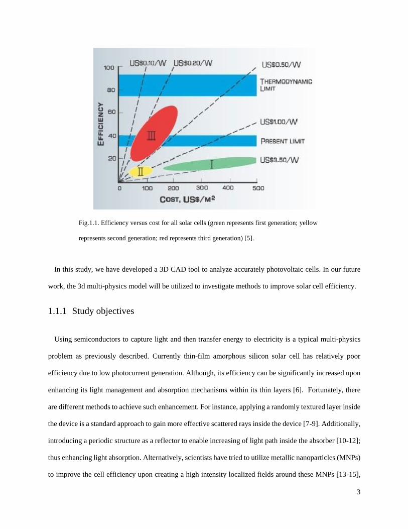
[3]. Fig.1.1 shows the efficiency and the cost for all three generations (the three generations are illustrated
in three different color) [5]. Fig. 1.1 indicates that the cost of the first generation exceeded $3.5/W while
the second in the range of $0.5-$1/W. Meanwhile, to compete with the current resources it should be less
than $0.20/W—which is the goal of the third generation. To develop the third generation, many
technologies have been recommended. The most popular one is using nanotechnology. Recently
nanotechnologies have been applied to photovoltaic technologies to help for improving the absorption of
light inside thin film photovoltaics (the second generation of photovoltaics). Using metallic nanoparticles
embedded inside photovoltaics (called Plasmon solar cells) with different shapes, sizes, and at different
positions inside solar cells could lead to a breakthrough for efficiency.
3
Fig.1.1. Efficiency versus cost for all solar cells (green represents first generation; yellow
represents second generation; red represents third generation) [5].
In this study, we have developed a 3D CAD tool to analyze accurately photovoltaic cells. In our future
work, the 3d multi-physics model will be utilized to investigate methods to improve solar cell efficiency.
1.1.1 Study objectives
Using semiconductors to capture light and then transfer energy to electricity is a typical multi-physics
problem as previously described. Currently thin-film amorphous silicon solar cell has relatively poor
efficiency due to low photocurrent generation. Although, its efficiency can be significantly increased upon
enhancing its light management and absorption mechanisms within its thin layers [6]. Fortunately, there
are different methods to achieve such enhancement. For instance, applying a randomly textured layer inside
the device is a standard approach to gain more effective scattered rays inside the device [7-9]. Additionally,
introducing a periodic structure as a reflector to enable increasing of light path inside the absorber [10-12];
thus enhancing light absorption. Alternatively, scientists have tried to utilize metallic nanoparticles (MNPs)
to improve the cell efficiency upon creating a high intensity localized fields around these MNPs [13-15],

4
unfortunately not much success has been reported yet. To investigate such effects, several groups around
the world have carried out many studies on solar cells’ performance enhancement by applying 1D and 2D
analysis [16-20]. However, for accurate modeling, rigorous 3D analysis [21-23] is required to resolve many
associated real practical fabrication problems. For example, only 3D multi-physics tools can be used to
analyze the effects of placing spherical MNPs, also accounting for the random polarization of rays (incident
waves), and considering their different multi-paths behaviors after being scattered from these randomly
shaped metallic nanoparticles. However, current CAD tools to model all the above structures/effects are
not adequate at this time. Table.1.1 shows different commercial CAD tools, their features. It compares
their capabilities and numerical methods to address solar cells multi-physics problems. It is understood that
solving such coupled 3D multi-physics problem (solar cell) is very challenging as it includes: light
propagation—an optics problem, energy absorption- a semiconductor problem, and light conversion to
photocurrent- an electrostatic problem. These three distinct physical fields need to be understood very well
initially and accurately modeled by utilizing a fast simulator and account for their coupling would follow.
In other words, we should able to predict the propagation of light within the different regions like dielectrics
(passive region), semiconductors (active region) plasmonic-nanoparticles (parasitic region), and study
effects of metals as reflectors/scatterers. Second, we have to to solve the physics of the semiconductor
devices so that we estimate the number of free electrons and holes. Finally, the third step is applying
electrostatic formulas to calculate the photocurrent that is collected by the two electrodes placed at both
sides of the device.
In this study, a 3D multi-physics toolbox has been developed to accurately model various types of solar
cells. The toolbox main features are given in Table.1.1, and its novelty is the 3D Model of plasmon
nanoparticles embedded inside semiconductors and the analysis of the effect of defects created by the
plasmon layer is included.
The main analysis concepts are explained in section 1.2, equations for the 3D problem are explained in
detail in section 1.7.1, supplemented by a description of the simulator initialization given in section 1.7.2

5
and a list of some major parameters required for electrical characteristic of solar cells is derived in section
1.7.3. Very promising preliminary results are included here.
1.1.1. 3D Model Development
To analyze a solar cell structure numerically by using finite element, first the 3D structure is drawn and
meshed using a non-uniform grid. Definitely, the accuracy and speed of simulation are completely
dependent on the selected mesh density. For instance, the critical regions like electrodes, semiconductor
junctions, plasmon, and sharp or tiny structures should be generated using very dense mesh (~ 𝜆50⁄ ). Next,
initial conditions for all variables and boundary conditions are set respectively to numerically solve the
partial differential equations (i.e. Maxwell’s equations, and the physics of the device transport equations).
Given that the solution of the nonlinear PDEs system is sensitive to these initial and boundary conditions,
finding a robust way to calculate large matrices is needed to achieve fast converging and accurate results.
For example, initializing the intensity of the impinging light (based on the latest published data for the Sun
spectrum), setting up correctly all electric parameters including the electro-optical material properties (like
complex refractive indices for semiconductors), and using a fast PDE solver are essential ingredients to get
an accurate realistic results.
In general, electromagnetic modeling is carried out by numerically solving Maxwell’s equations using
one of the available techniques [24-28], like a finite element method that has been applied here. Meanwhile,
to model the metallic nanoparticles Drude-Lorentz dispersion model [37] has been utilized here.
Subsequently, the result of this EM simulation is used to calculate the light power intensity distribution
inside the semiconductor region (active layer). Then, the number of electron-hole pairs is estimated as a
function of the previously calculated light intensity using chemical absorption data [42]. In our analysis,
the free charge carriers’ recombination due to different factors (free carrier life time, energy trap level, and
density of carrier concentrations) are considered, as they could cause significant impact in predicting the
final results. Keep in mind that the recombination rate is a strong function of both the doping concentration
6
and density of defects inside the semiconductor. As a final step, the number of electron-hole pairs captured
by the two electrodes at both sides of the active region is calculated using Poisson's Electrostatics Equation.
Meanwhile, other major parameters like external quantum efficiency, solar cell efficiency, J-V curve, and
fill factor can be extracted as well as by-products [34-36]. A step-by-step illustration of the above
calculations are given in section 1.7.
1.2. Theories
1.2.1. Solving solar cell problem in 3D
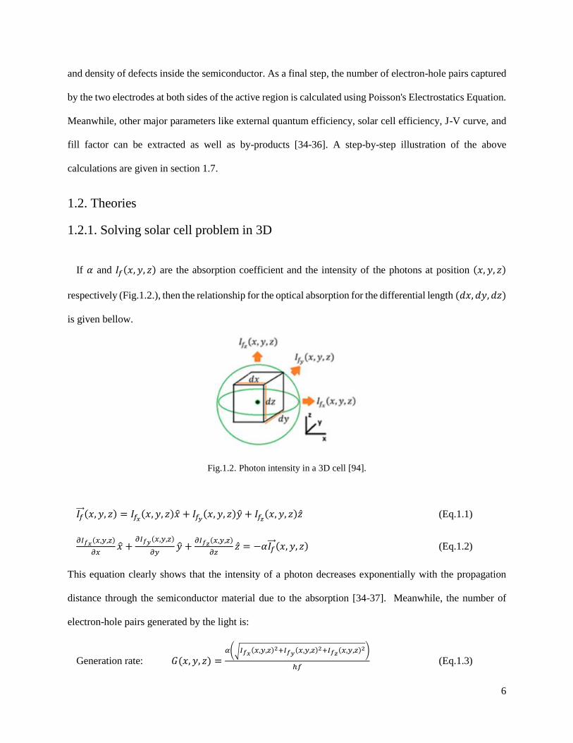
If 𝛼 and 𝐼𝑓(𝑥, 𝑦, 𝑧) are the absorption coefficient and the intensity of the photons at position (𝑥, 𝑦, 𝑧)
respectively (Fig.1.2.), then the relationship for the optical absorption for the differential length (𝑑𝑥, 𝑑𝑦, 𝑑𝑧)
is given bellow.
Fig.1.2. Photon intensity in a 3D cell [94].
𝐼𝑓 (𝑥, 𝑦, 𝑧) = 𝐼𝑓𝑥(𝑥, 𝑦, 𝑧)𝑥 + 𝐼𝑓𝑦(𝑥, 𝑦, 𝑧)�� + 𝐼𝑓𝑧(𝑥, 𝑦, 𝑧)�� (Eq.1.1)
𝜕𝐼𝑓𝑥(𝑥,𝑦,𝑧)
𝜕𝑥𝑥 +
𝜕𝐼𝑓𝑦(𝑥,𝑦,𝑧)
𝜕𝑦�� +
𝜕𝐼𝑓𝑧(𝑥,𝑦,𝑧)
𝜕𝑧�� = −𝛼𝐼𝑓 (𝑥, 𝑦, 𝑧) (Eq.1.2)
This equation clearly shows that the intensity of a photon decreases exponentially with the propagation
distance through the semiconductor material due to the absorption [34-37]. Meanwhile, the number of
electron-hole pairs generated by the light is:
Generation rate: 𝐺(𝑥, 𝑦, 𝑧) =𝛼(√𝐼𝑓𝑥
(𝑥,𝑦,𝑧)2+𝐼𝑓𝑦(𝑥,𝑦,𝑧)2+𝐼𝑓𝑧
(𝑥,𝑦,𝑧)2)
ℎ𝑓 (Eq.1.3)
7
Where h is plank constant, and f is frequency of the wave. Subsequently, to calculate the free electron
and hole density, Poisson’s Equation is used:
�� . �� 𝜑 = −𝑞
𝜀(𝑝 − 𝑛 + 𝑐) PDE:
𝜕2𝜑
𝜕𝑥2 +𝜕2𝜑
𝜕𝑦2 +𝜕2𝜑
𝜕𝑧2 = −𝑞
𝜀(𝑝 − 𝑛 + 𝑐) (Eq.1.4)
Shockley Read Hall recombination rate (Eq.1.5- Eq.1.9):
∆𝐸𝑡 = 𝐸𝑡 − 𝐸𝑖 (Eq.1.5)
𝑛1 = 𝛾𝑛√𝑁𝑐𝑁𝑣𝑒𝑥𝑝 (−𝐸𝑔−∆𝐸𝑔
2𝑉𝑡ℎ) 𝑒𝑥𝑝 (
∆𝐸𝑡
𝑉𝑡ℎ) (Eq.1.6)
𝑝1 = 𝛾𝑝√𝑁𝑐𝑁𝑣𝑒𝑥𝑝 (−𝐸𝑔−∆𝐸𝑔
2𝑉𝑡ℎ) 𝑒𝑥𝑝 (
∆𝐸𝑡
𝑉𝑡ℎ) (Eq.1.7)
𝑛𝑖 = 𝛾𝑛𝛾𝑝√𝑁𝑐𝑁𝑣𝑒𝑥𝑝 (−𝐸𝑔−∆𝐸𝑔
2𝑉𝑡ℎ) (Eq.1.8)
𝑅(𝑥, 𝑦, 𝑧) = 𝑅𝑛(𝑥, 𝑦, 𝑧) = 𝑅𝑃(𝑥, 𝑦, 𝑧) =𝑛𝑝−𝑛𝑖
2
𝜏𝑝(𝑛1+𝑛)𝜏𝑛(𝑝1+𝑝) (Eq.1.9)
Total rate: 𝑅𝑡(𝑥, 𝑦, 𝑧) = 𝐺(𝑥, 𝑦, 𝑧) − 𝑅(𝑥, 𝑦, 𝑧) (Eq.1.10)
Transport of Diluted species (Electron)
PDE: �� .𝐽𝑛 − 𝑞𝜕𝑛
𝜕𝑡− 𝑞
𝜕𝜌𝑛
𝜕𝑡= q𝑅𝑡(𝑥, 𝑦, 𝑧)
𝜕𝐽𝑛𝑥
𝜕𝑥+
𝜕𝐽𝑛𝑦
𝜕𝑦+
𝜕𝐽𝑛𝑧
𝜕𝑧− 𝑞
𝜕𝑛
𝜕𝑡− 𝑞
𝜕𝜌𝑛
𝜕𝑡= q𝑅𝑡(𝑥, 𝑦, 𝑧) (Eq.1.11)
PDE: 𝐽𝑛 = 𝐽𝑛𝑥 + 𝐽𝑛𝑦
+ 𝐽𝑛𝑧 (Eq.1.12)
𝐽𝑛 = (−𝑞𝑛𝜇𝑛𝜕𝜑
𝜕𝑥+ 𝑞𝐷𝑛𝑥
𝜕𝑛
𝜕𝑥) 𝑥 + (−𝑞𝑛𝜇𝑛
𝜕𝜑
𝜕𝑦+ 𝑞𝐷𝑛𝑦
𝜕𝑛
𝜕𝑦) 𝑦 + (−𝑞𝑛𝜇𝑛
𝜕𝜑
𝜕𝑧+ 𝑞𝐷𝑛𝑧
𝜕𝑛
𝜕𝑧) 𝑧
Space charge density (Electron): 𝜌𝑛 = −𝑞
𝜀𝑛 (Eq.1.13)
where 𝜑 (Electric Potential), 𝑝 (Hole concentration), and 𝑛 (Electron concentration) are variables, 𝑞
(Electron charge), 𝜀 (Optical property of the material), 𝑐 (Initial value for carrier concentration), ni (intrinsic
concentration), 𝜏𝑛(Electron life time), 𝜏𝑝 (Hole life time) , 𝜑0 (incident photon flux), 𝛼 (absorption
coefficient of material), 𝜇𝑛 (Electron mobility), 𝜇𝑝 (Hole mobility), and 𝐷𝑛 (Electron Diffusivity) are
constant value. γn and γp are the electron and hole degeneracy factors, Nc and Nv are the effective densities
of states for the conduction and valence band, 𝐸𝑔 is the band-gap and ∆𝐸𝑔 the band gap narrowing. 𝐸𝑡 is
8
the trap energy level. Energy difference between the defect level and the intrinsic level is ∆𝐸𝑡. The same
equations can be derived for holes. After using coupling equations (Eq.1.11), (Eq.1.12), and (Eq.1.13), there
will be only two non-linear PDEs (Eq.1.14), (Eq.1.15).
−𝑛𝜇𝑛 (−𝑞
𝜀(𝑝 − 𝑛 + 𝑐)) + 𝐷𝑛𝑥
𝜕2𝑛
𝜕𝑥2 + 𝐷𝑛𝑦𝜕2𝑛
𝜕𝑦2 + 𝐷𝑛𝑧𝜕2𝑛
𝜕𝑧2 + (−1 +𝑞
𝜀)
𝜕𝑛
𝜕𝑡= 𝑅𝑡(𝑥, 𝑦, 𝑧) (Eq.1.14)
𝑝𝜇𝑝 (−𝑞
𝜀(𝑝 − 𝑛 + 𝑐)) − 𝐷𝑝𝑥
𝜕2𝑝
𝜕𝑥2 − 𝐷𝑝𝑦𝜕2𝑝
𝜕𝑦2 − 𝐷𝑝𝑧𝜕2𝑝
𝜕𝑧2 + (1 +𝑞
𝜀)
𝜕𝑝
𝜕𝑡= −𝑅𝑡(𝑥, 𝑦, 𝑧) (Eq.1.15)
Gaussian distribution (for both acceptor and donor) is considered as a dopant distribution. The junction
depths in x, y, and z direction are set at 2um, 2um, and 300[nm] respectively.
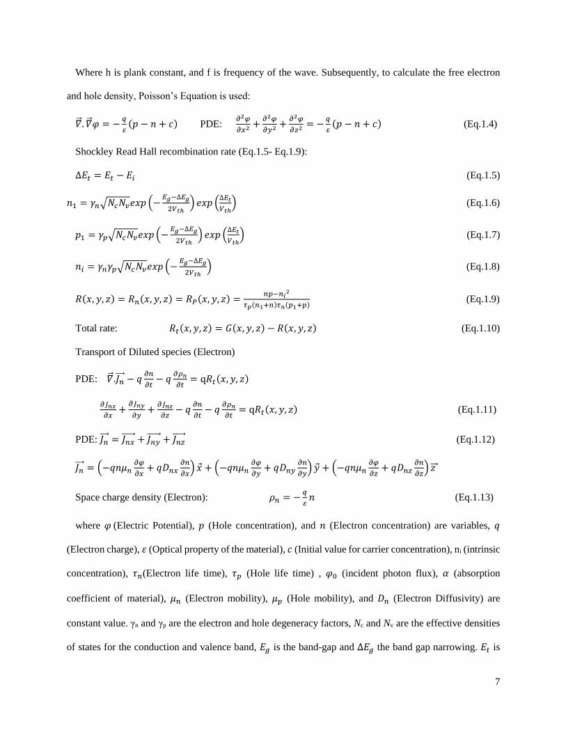
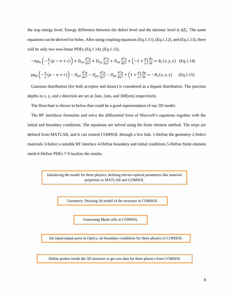
The flowchart is shown in below that could be a good representation of our 3D model.
The RF interfaces formulate and solve the differential form of Maxwell’s equations together with the
initial and boundary conditions. The equations are solved using the finite element method. The steps are
defined from MATLAB, and it can control COMSOL through a live link. 1-Define the geometry 2-Select
materials 3-Select a suitable RF interface 4-Define boundary and initial conditions 5-Define finite element
mesh 6-Define PDEs 7-Visualize the results.
Initializing the model for three physics; defining electro-optical parameters like material
properties in MATLAB and COMSOL
Geometry: Drawing 3d model of the structure in COMSOL
Generating Mesh cells in COMSOL
Set input/output ports in Optics; set boundary conditions for three physics in COMSOL
Define probes inside the 3D structure to get raw data for three physics from COMSOL
9
Fig.1.3. Tetrahedral Mesh Generation of the 3D device for one unit cell [94].
Define excitation for Optics in COMSOL from MATLAB main code
Define PDEs for three physics (Maxwell, Continuity, Poisson equations, generation and
recombination rates) in COMSOL
Couple the solvers through MATLAB (main code), and also managing the solvers (inside the COMSOL)
sequentially
Is the
solution
converged?
Change mesh resolution in sensitive locations
inside 3D structure in COMSOL No
Yes
Extract the output data from COMSOL, and post processing in MATLAB and COMSOL

10
To minimize the amount of physical memory (RAM) for computation and speed up computation we can
use periodic boundary conditions along x, and y axis, which means that we solve equations for only one
unit cell. Tetrahedral has been chosen as a type of mesh. Sharp edges or small particles like MNPs should
be generated with high mesh density. Also the mesh size physically placed close to the critical edges (p
and n type region) should be considered fine to make sure the PDEs solver is converged properly (Fig.1.3.).
1.2.2. Initialization of the simulator
In order to solve these partial differential equations, all parameters are needed to be initialized. The
electro-optical properties like dielectric constant, refractive indices (real part and imaginary part),
electron/hole mobility and the other electronic properties have been extracted from [17], [29-33]. In case
of using MNPs or a plasmon layer the dielectric constant value has to be calculated for each optical
wavelength of interest. For gold or silver NPs, optical constants were measured and given by Drude [38].
Drude-Lorentz dispersion model is a well-known model and is given by
(Eq.1.16)
Additional references can be used like [39-40] to double check materials properties.
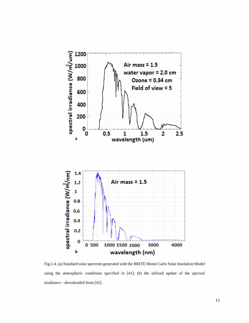
Generally, the spectrum of incident light and intensity of impinging on the device is the most important
initializing step to get accurate results from the simulation. Because some of the simulation outputs (like
solar cell efficiency, and short circuit current) are directly related to the impinging light intensity as a
function of wavelength, we needed then to utilize very accurate data. Hence, we utilized the spectral
irradiance chart that has been measured several times and published by NASA [41] (Fig.1.18. (a)). But, we
need to keep in mind that the spectral irradiance depends on different factors like: the height from the sea
level, water vapor, and air pollution. It is time dependent as well. For simplicity, we assume as a constant
for the time being. (Fig.1.4. (b)) shows the latest update that was found from [42], and utilized in our
simulator.
2
2 2
1
, 0
M
j p
r
j o j j
f
i
11
Fig.1.4. (a) Standard solar spectrum generated with the BRITE Monte Carlo Solar Insolation Model
using the atmospheric conditions specified in [41]; (b) the utilized update of the spectral
irradiance—downloaded from [42].

12
1.2.3. Electrical outputs
Our model can be used to calculate many parameters like: External Quantum Efficiency (EQE), Solar
Cell Efficiency, open circuit voltage, and short circuit [34-35].
The external quantum efficiency (EQE) is defined as:
𝐸𝑄𝐸(𝑤𝑎𝑣𝑒𝑙𝑒𝑛𝑔𝑡ℎ) =𝑛𝑢𝑚𝑏𝑒𝑟 𝑜𝑓 𝑒𝑙𝑒𝑐𝑡𝑟𝑜𝑛𝑠 𝑖𝑠 𝑐𝑜𝑙𝑙𝑒𝑐𝑡𝑒𝑑 𝑏𝑦 𝑒𝑙𝑒𝑐𝑡𝑟𝑜𝑑𝑒
𝑛𝑢𝑚𝑏𝑒𝑟 𝑜𝑓 𝑝ℎ𝑜𝑡𝑜𝑛𝑠 𝑙𝑖𝑔ℎ𝑡 𝑠𝑜𝑢𝑟𝑐𝑒 (Eq.1.17)
The short-circuit current density can be computed as:
𝐽𝑠𝑐 = 𝑐ℎ𝑎𝑟𝑔𝑒 𝑜𝑓 𝑒𝑙𝑒𝑐𝑡𝑟𝑜𝑛 × 𝑛𝑢𝑚𝑏𝑒𝑟 𝑜𝑓 𝑒𝑙𝑒𝑐𝑡𝑟𝑜𝑛𝑠 𝑐𝑜𝑙𝑙𝑒𝑐𝑡𝑒𝑑 𝑏𝑦 𝑒𝑙𝑒𝑐𝑡𝑟𝑜𝑑𝑒 (Eq.1.18)
Solar Cell Efficiency is: 𝐸𝑓𝑓𝑖𝑐𝑖𝑒𝑛𝑐𝑦 = 𝐽𝑠𝑐 𝑉𝑜𝑐 𝐹𝐹
𝑃𝑖𝑛 (Eq.1.19)
FF is the filling factor, which can be derived from J-V curve of the device.
𝐹𝐹 = 𝐼𝑚 𝑉𝑚
𝐼𝑠𝑐 𝑉𝑜𝑐 (Eq.1.20)
1.3. Simulated and measured results-no plasmon
For model validation, the simulation results for a thin film P-I-N solar cell model was compared to
previously published measured results [14]. However, some material properties were not cited on this
publication and their values were assumed here based on well-known references like [17] and [29-33].
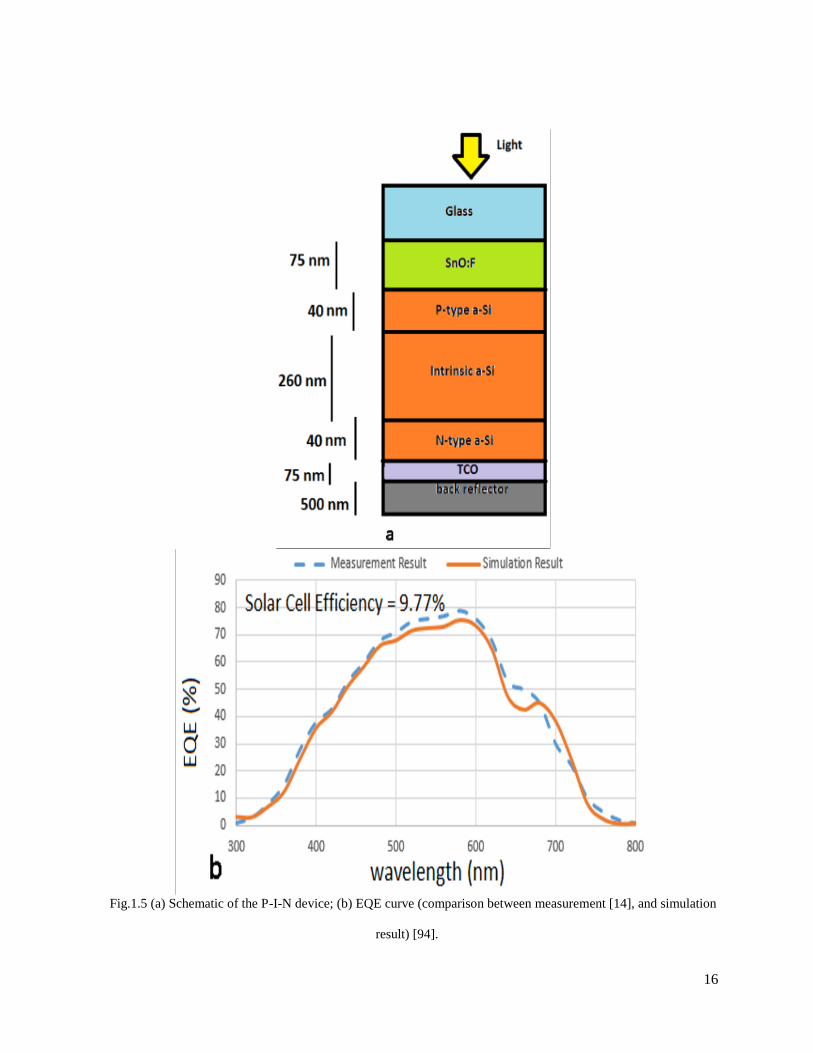
The structure of the modelled solar cell shown in Fig.1.5 (a) consists of five stacked layers: a Glass (for
protection) on top, SnO:F TCO (transparent conductive oxide), followed by absorber layers (a-Si:H) as a
P-I-N structure, then a TCO on the back, and all on top of a back reflector.
The Amorphous silicon has 260 nm-thick intrinsic layer, the front electrode has a 75 nm-thick (SnO:F)
layer, and the back electrode (AZO) is 75 nm-thick layer on top of the reflector.
The N+ and P+ layers are modelled here too as 40 nm thick layer each. Fig.1.5 (b) shows a comparison
between the simulated and measured EQE results, where only a slight discrepancy is seen. But given that
most of the material parameters were obtained from well-known references (listed in Table.1.2) but their

13
real values could be within a specified uncertainty range; also the physical layers dimensions were guessed
based on the intended design but could deviate slightly from the really fabricated ones. In addition, the
dopant distribution and the density of the traps (recombination) were not listed in the experimental
description and were assumed as well.
Fortunately, the simulated results are still indicating a similar behavior to the experimentally
demonstrated ones. The solar efficiency and fill factor FF were used as a base line for comparison and their
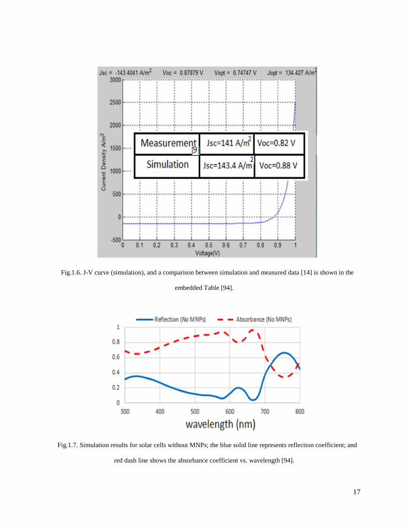
values were 9.77%, and 74% respectively, and the maximum EQE occurs at 580nm. The calculated current
density as a function of voltage is shown in Fig.1.6. Additionally, the measured and simulated short circuit
current Jsc and the open circuit voltage Voc were listed too.
Additional parameters including the reflection and absorbance coefficient were calculated for the whole
solar cell as a function of wavelength and are shown in Fig.1.7. The transmission coefficient however, is
almost zero.
When comparing Fig.1.7 and Fig.5 (b), the level of light absorbance coefficient in some regions of the
spectrum is higher than what is indicated by the EQE curve. This difference demonstrates that the energy
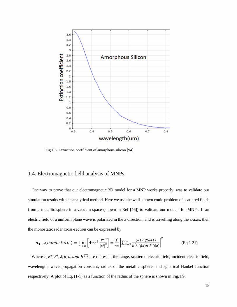
wasn’t totally converted to current and this drop is due to internal device losses. Fig.1.8. represents the
extinction coefficient of amorphous silicon calculated based on [48], and it can be observed that the
absorbance of light inside the amorphous silicon increases at higher frequencies. For this reason in the UV
region most of the impinging solar energy on the cell is absorbed at the top layer of the semiconductor (P+
region) before approaching the depletion region. It turns out that the probability of creating free electron-
hole pairs outside the depletion region increases; thus unfortunately increasing the probability of free carrier
recombination immediately and this would be an energy loss. But, if the light could propagate for a longer
path inside the semiconductor, it can generate free electron hole pairs inside the depletion region,
subsequently the electrostatic electric field (created based on majority carriers in the depletion region) could
cause charge separation (electrons and holes) creating electricity. In other words, the presence of material
defects inside the semiconductors can elevate the recombination probability of free carriers as well and
reduce the overall conversion efficiency.
14
Table.1.1. Introduce some commercial CAD Tools were used to solve solar cells’ model [94].
Reference Tools Analysis
Method
Type of
modeling
Validation Problem solved
[21]
HFSS
FEM
Optical model
Validated by
another CAD
tool (ASA)
3D modeling of
Single junction
thin film silicon
Solar cells with
flat surface and
1D, and 2D
modeling of
trapezoid-
shaped surface
[19]
SCAPS
Numerical
methods
(Newton)
Semiconductor
and
Electrostatic
1D modeling of
Polycrystalline
thin film solar
cells, The
problem of
transients of
current to time
dependent bias
conditions is
solved
[20]
D-AMPS-1D (1D
simulation program
Analysis of
Microelectronic and
Photonic Devices)
Finite
differences
(Newton
Raphson
iteration
method)
Semiconductor
and
Electrostatic
Validated by
measurement
1D modeling of
structures such
as homo-
junctions,
heterojunctions,
multi-junctions,
and Ge
photovoltaic
devices
[23]
FDTD Solution
TCAD Sentaurus
FDTD
FEM
Multi-physics
Thin film
amorphous
silicon; existing
metallic
nanoparticles at
back of P-I-N
Our
Approach
COMSOL+MATLAB
FEM
Multi-physics
Validated by
measurement
Thin film
amorphous
silicon;
existing
metallic
nanoparticles
inside P-I-N
and
3D modeling of
trapezoid-
shaped surface

15
Table.1.2. the utilized value of each parameter for the utilized validation example.
Parameter –Name Value
T(temperature) 300[K]
Ni -Ref[33] 0.949x10⁶ [cm-3]
Doping (N+) 1x10²⁰[cm-3]
Doping (P+) 1021[cm-3]
Thickness (N+, a-Si)-Ref [14] 40 [nm]
Thickness (intrinsic, a-Si)- Ref [14] 260 [nm]
Thickness (P+, a-Si)- Ref [14] 40 [nm]
Thickness (AZO) -( TCO in front)- Ref [14] 75[nm]
Thickness (glass)- Ref [14] 200[um]
Thickness (Air)- Ref [14] 20[um]
Thickness -(TCO BACK)- Ref [14] 75[nm](AZO)
Thickness (Silver) Reflector back- Ref [14] 500[nm]
Electron mobility, a-Si -intrinsic-Ref [17] 20[cm2/( V s)]
Hole mobility, a-Si -intrinsic-Ref [17] 2[cm2/( V s)]
Electron mobility, a-Si N+-Ref [17] 20[cm2/( V s)]
Hole mobility, a-Si N+-Ref [17] 2[cm2/( V s)]
Electron mobility, a-Si P+-Ref [17] 20[cm2/( V s)]
Hole mobility, a-Si P+-Ref[17] 2[cm2/(V s)]
Electron Life time, a-Si -intrinsic-Ref [32, 33] 20[ns]
Hole Life time, a-Si -intrinsic-Ref [32, 33] 20[ns]
Electron Life time, a-Si N+-Ref [32, 33] 0.0001[ns]
Hole Life time, a-Si N+-Ref [32, 33] 10[ns]
Electron Life time, a-Si P+-Ref [25,26] 10[ns]
Hole Life time, a-Si P+-Ref [25,26] 0.0001[ns]
Density Of State Valence band, a-Si –Ref [30] 2.5x10²⁰[cm-3]
Density Of State Conduction band, a-Si –Ref [30] 2.5x10²⁰[cm-3]
Difference between Defect level and intrinsic level N+,P+-Ref [34] 0.7
Difference between Defect level and intrinsic level intrinsic-Ref [34] 0.3
Energy Band gap a-Si-Ref [33] 1.74
diameter silver NPs-Ref [14] 20[nm]
Affinity, a-Si (electro affinity)-Ref [17] 4.00eV
Incident Light Angle 0 [deg]
16
Fig.1.5 (a) Schematic of the P-I-N device; (b) EQE curve (comparison between measurement [14], and simulation
result) [94].
17
Fig.1.6. J-V curve (simulation), and a comparison between simulation and measured data [14] is shown in the
embedded Table [94].
Fig.1.7. Simulation results for solar cells without MNPs; the blue solid line represents reflection coefficient; and
red dash line shows the absorbance coefficient vs. wavelength [94].
18
Fig.1.8. Extinction coefficient of amorphous silicon [94].
1.4. Electromagnetic field analysis of MNPs
One way to prove that our electromagnetic 3D model for a MNP works properly, was to validate our
simulation results with an analytical method. Here we use the well-known conic problem of scattered fields
from a metallic sphere in a vacuum space (shown in Ref [46]) to validate our models for MNPs. If an
electric field of a uniform plane wave is polarized in the x direction, and is travelling along the z-axis, then
the monostatic radar cross-section can be expressed by
𝜎3−𝐷(𝑚𝑜𝑛𝑜𝑠𝑡𝑎𝑡𝑖𝑐) = lim𝑟→∞
[4𝜋𝑟2 |𝐸𝑠|2
|𝐸𝑖|2] =
𝜆2
4𝜋|∑
(−1)𝑛(2𝑛+1)
𝐻(2) (𝛽𝑎)𝐻(2)(𝛽𝑎)
∞𝑛=1 |
2
(Eq.1.21)
Where 𝑟, 𝐸𝑠, 𝐸𝑖 , 𝜆, 𝛽, 𝑎, 𝑎𝑛𝑑 𝐻(2) are represent the range, scattered electric field, incident electric field,
wavelength, wave propagation constant, radius of the metallic sphere, and spherical Hankel function
respectively. A plot of Eq. (1-1) as a function of the radius of the sphere is shown in Fig.1.9.

19
Fig.1.9. Normalized monostatic radar cross section for a conducting sphere as a function
of sphere radius [47].
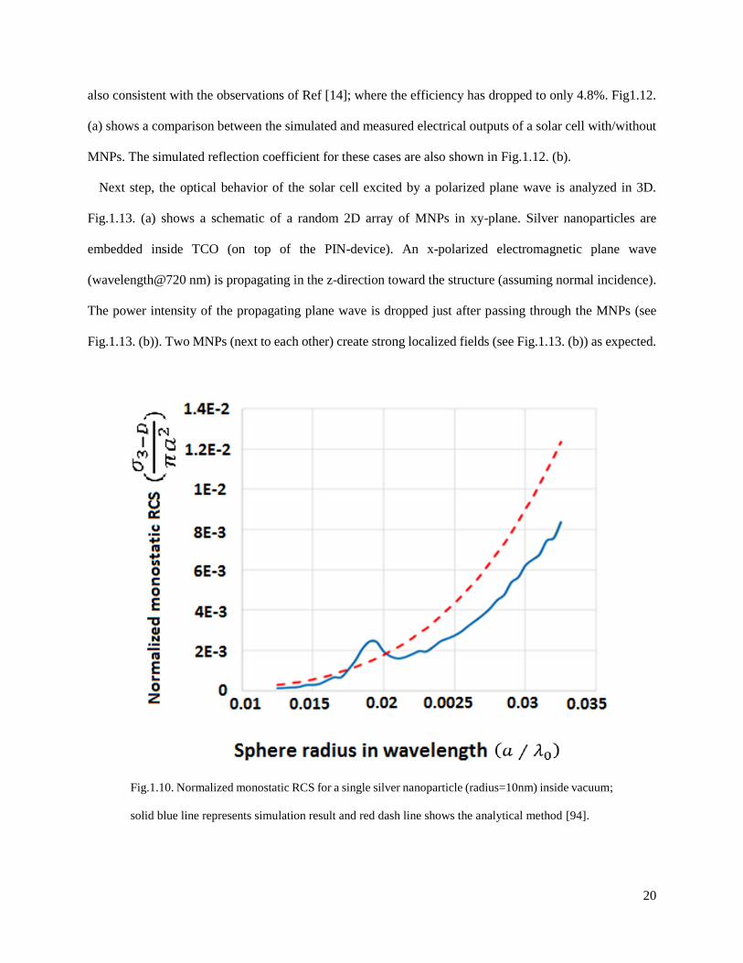
The results can be divided into three regions; the Rayleigh, the Mie (or resonance), and the optical region.
The Rayleigh region represents the part of the curve for small radii values (a < 0.1λ). Hence in the Rayleigh
region, Eq. (1) can be reduced to 𝜎3−𝐷(𝑚𝑜𝑛𝑜𝑠𝑡𝑎𝑡𝑖𝑐) ≅9𝜆2
4𝜋(𝛽𝑎)6 (Eq.1.22)
Hence, we compared our 3D model for a sphere in vacuum and the analytical method and results are
shown in Fig.1.10. A good accuracy is seen for the long wavelengths region. Some slight deviation is
however seen for longer wavelength but still adequate for our modeling efforts here. To improve our model
at long wavelength, finer mesh can still be used but will significantly reduce computation speed.
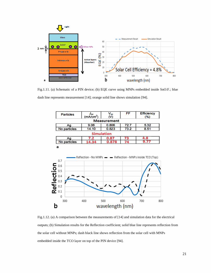
1.5. Simulated and measured results-with plasmon
Our next step was to analyze the effect of adding silver nanoparticles in each layer; one layer at a time to
determine the optimum location and position that would enhance the solar cell efficiency. In our model,
silver nanoparticles are modelled as spheres with 10nm radius [14] and are arranged in a random 2D array
(in xy-plane) with a maximum center to center spacing of 50 nm. Initially, these silver NPs were placed 2
nm above the absorber layer along the SnO:F P-type A-Si interface as shown in Fig.1.11. (a) as suggested
by [14]. But this resulted in a pronounced drop in solar cell efficiency as noticed in Fig.1.11. (b), which is
20
also consistent with the observations of Ref [14]; where the efficiency has dropped to only 4.8%. Fig1.12.
(a) shows a comparison between the simulated and measured electrical outputs of a solar cell with/without
MNPs. The simulated reflection coefficient for these cases are also shown in Fig.1.12. (b).
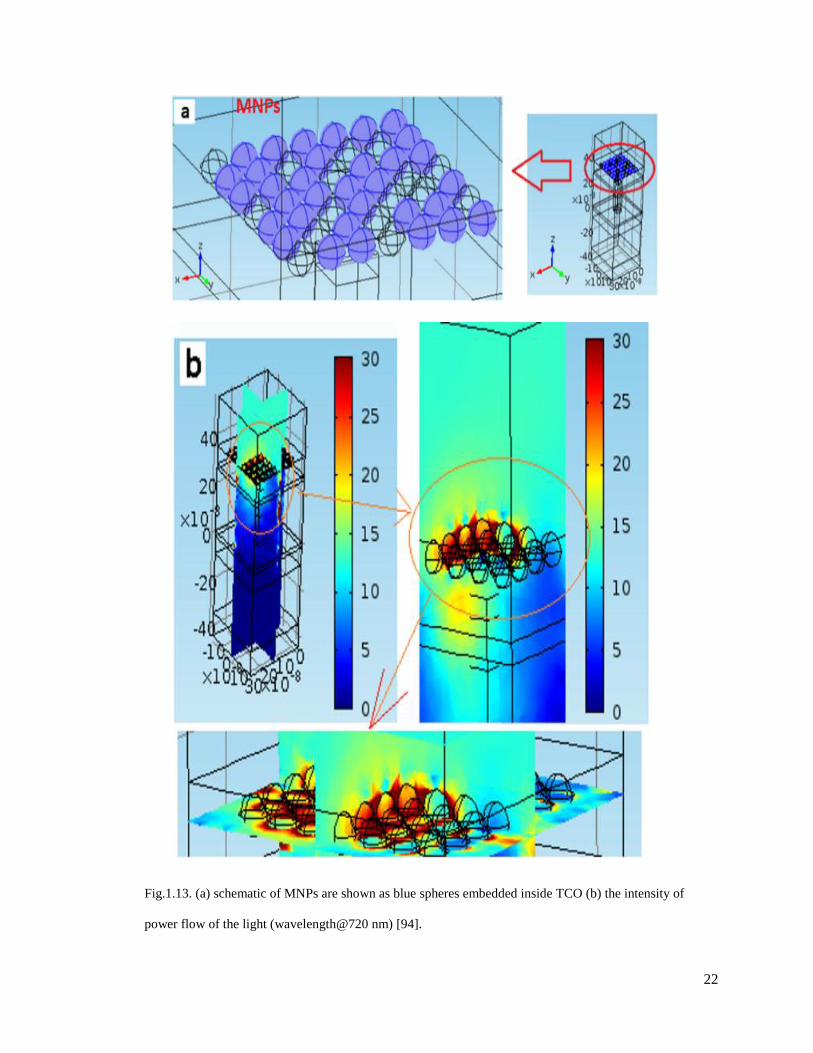
Next step, the optical behavior of the solar cell excited by a polarized plane wave is analyzed in 3D.
Fig.1.13. (a) shows a schematic of a random 2D array of MNPs in xy-plane. Silver nanoparticles are
embedded inside TCO (on top of the PIN-device). An x-polarized electromagnetic plane wave
(wavelength@720 nm) is propagating in the z-direction toward the structure (assuming normal incidence).
The power intensity of the propagating plane wave is dropped just after passing through the MNPs (see
Fig.1.13. (b)). Two MNPs (next to each other) create strong localized fields (see Fig.1.13. (b)) as expected.
Fig.1.10. Normalized monostatic RCS for a single silver nanoparticle (radius=10nm) inside vacuum;
solid blue line represents simulation result and red dash line shows the analytical method [94].
21
Fig.1.11. (a) Schematic of a PIN device; (b) EQE curve using MNPs embedded inside SnO:F.; blue
dash line represents measurement [14]; orange solid line shows simulation [94].
Fig.1.12. (a) A comparison between the measurements of [14] and simulation data for the electrical
outputs; (b) Simulation results for the Reflection coefficient; solid blue line represents reflection from
the solar cell without MNPs; dash black line shows reflection from the solar cell with MNPs
embedded inside the TCO layer on top of the PIN device [94].
22
Fig.1.13. (a) schematic of MNPs are shown as blue spheres embedded inside TCO (b) the intensity of
power flow of the light (wavelength@720 nm) [94].

23
1.6. Conclusion
Here an effective rigorous 3-D multi-physics modeling of solar cells was presented. Our developed
simulator is a real multi-physics modeling toolbox that is comprised of three coupled modules: Optics,
carrier transport in semiconductors, and Electrostatic. To solve their associated nonlinear partial differential
equations (PDEs) in 3D, we used two commercial tools (COMSOL, and MATLAB). One of the main
reasons to carry out this 3D simulation is to accurately predict the electric field distribution due to the light
scattering of the 3D plasmonic particles excited by the randomly polarized sun light. Our 3D tool has been
validated by comparing its results with published measured ones.
The comparison between both measured and simulated results indicates a very good agreement even
though some material parameters were assumed like the dopant distribution, and the density of traps
(recombination), in addition to some assumed layers’ thicknesses. The developed toolbox has been used to
observe some major phenomena like strong localized fields around the MNPs. In the next chapter we will
show that some techniques to get significant efficiency improvement and to address the defect degradation
issue as well.

24
CHAPTER 2
Strategies for Designing Highly Efficient Thin Film
Amorphous Silicon Solar Cells
2.1. Introduction
Significant manufacturing cost reduction of solar cells can be achieved by using thin film hydrogenate
amorphous silicon (A-Si:H) instead of bulk silicon. However, a pronounced efficiency drop could be
incurred by utilizing thin film silicon [1] instead of the bulk silicon. Typically, applying thin film solar cells
suffers from a significant reduction of light absorption within the semiconductor structure, as well as
pronounced efficiency drop due to inherent surface reflection.
To achieve higher efficiency, some boosting techniques have been developed targeting better light
absorption. These enhancement methods are based on increasing path light lengths and implanting
scatterers within the cells that are designed for constructive interference. Random textured or corrugated
external/internal interfaces are used to enhance scattering [2-8], while transparent conductive oxide layers
(TCO) are utilized to minimize reflections at the interfaces, while highly reflective back surfaces are used
to enhance back reflections. Fig. 2.1 illustrates such enhancing techniques. Simulations have indicated the
feasibility of achieving stronger absorption, and henceforth-higher efficiency.
Alternatively, MNPs are placed within solar cells. MNPs (few nanometers in diameter) can scatter a wide
range of visible light, and also can create high intensity near fields in their vicinity.
Typically, the optical properties of MNPs are highly controlled by changing their size [9], density [10,
15], conductivity [9], location [11, 16], and shape [12-14]. These MNPs can be made out of gold or silver,

25
and both could exhibit great metal/plasmon behavior at optical frequencies and consequently would impact
amorphous silicon thin film solar cell’s performance [11] significantly.
Fig.2.1. Paths of light inside solar cells for different type of electrodes [95].
Several studies have utilized nanotechnology to fabricate MNPs and implant them within solar cells.
Based on various simulations, a significant performance improvement is predicted when adding MNPs.
Unfortunately, serious parasitic losses and structure defects were associated with these MNPs implantation,
and have led to significant overall solar cell efficiency degradation. So the search is still on to explore the
feasibility of finding an efficient light scattering scheme within these solar cells whenever MNPs are
carefully placed within the structure to increase light propagation path lengths and better absorption, while
minimizing energy loss. To combat the efficiency drop, we need to address some challenging design issues
like: optical losses within MNPs, and those due to fabrication defects. The optical loss is manifested by a
large fraction of the impinging light energy absorbed by MNPs and converted to phonons, thus significantly
reducing the overall efficiency. Add to that, during the fabrication process, gross material defects can occur
and would spread around embedded MNPs causing pronounced loss. So these design/fabrication issues
need to be resolved first to enhance efficiency. Several investigations have been carried out to understand
26
the role of these embedded nanoparticles and their potential on performance improvements [9-11].
However, certainly further studies are still needed, given that the impact of MNPs has not been
experimentally materialized yet and the need has significantly increased to reveal a successful design recipe.
Along these lines, we carried out a 3D multi-physics modeling of plasmon solar cells [17], and have studied
the effect of MNPs on performance in search for efficiency enhancement. In this paper, new design rules
for embedding MNPs inside thin film amorphous silicon solar cells have been presented that would lead to
solar cell efficiency enhancement. A modeling toolbox was successfully developed for 3D solar cells
performance analysis, and has been validated as well using previously published experimental data carried
out by Ref. [11]. In this paper a brief introduction for developing the 3D modeling tool will be presented in
the Appendix. The effect of placing MNPs at different locations (front, middle, and back of the PIN solar
cell) to maximize the photocurrent generation will be discussed in section II. Finally, a new design
methodology will be recommended in sections III and IV. Conclusion will be given in section V.
2.2. Simulation analysis
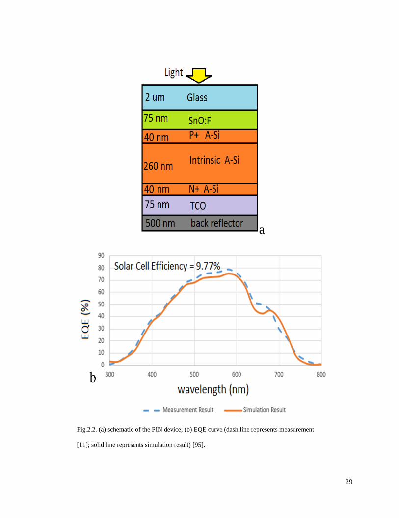
A 3D model of a thin film amorphous silicon solar cell has been developed which accounts for surface
roughness as well, a microscopic view of the structure is shown in Fig. 2.2 (a). The surface roughness would
significantly impact the overall performance and typically, the amount of surface roughness is related to
transparent conductive oxide (TCO) type and thickness. For instance, using TCO film with large grains
would increase the surface roughness [24-26]. At the same time, the size of the grains is correlated to the
thickness of the thin film TCO layer, where a thinner film may have less surface roughness [24-26]. For
instance, the thickness of the thin film TCO, considered for this model, is 75nm, and its surface roughness
is estimated to be less than 10nm.
In our investigation, to model the solar cell and take the effect of surface roughness into account, a 3D
device model is used where a trapezoidal grating is assumed. Here, for example, a periodic structure of a
trapezoidal shape (like that of [27]) with a 30° degree slope in each side, and a10nm height (with periodicity
of 200 nm) is assumed and implemented to model the 3D gratings of the solar cell of [11]. Based on these

27
calculations, a comparison between our simulated External Quantum Efficiency (EQE) results and that
measured by [11] is shown in Fig. 2(b). Only a slight discrepancy is seen-- thus validating our models. This
success establishes the logistics to extrapolate models that include MNPs effects and the impact of their
size, shape, and location of the device layers on solar cell efficiency. To understand the effect of adding
silver nanoparticles, we analyzed solar cell performance after embedding these MNPs at different layers,
one layer at a time. In our model, silver NPs are modelled as spheres with 18nm diameter and arranged in
a random 2D array with a maximum center-to-center spacing of 36 nm. First, we embedded MNPs inside
the absorber region as seen in Fig. 3(a), and our simulation results (shown in Fig. 3 (b)) indicate a rather
significant drop in efficiency which is once more consistent with Ref. [11] observations.
The agreement seen in Fig 2.3 between simulation and measurement is good validating again our models,
although surprisingly, the efficiency has dropped to 3.5% in contradiction to the common belief that it
should be enhanced upon using MNPs-- (however, if no defects exist, the efficiency though would be 9.77%
as indicated in Fig. 2.2).
Second, we continued modeling for cases of MNPs that were moved from the top of the intrinsic layer to
its bottom, however the solar cell efficiency still dropped even further to 2.55% (see Fig. 2.3 (b)), which is
related to effect of defects.
2.3. Impact defects
One of the disadvantages of embedding MNPs inside semiconductor is the increase in the density of
defects especially around the MNPs. Presence of defects causes pronounced increase in optical losses. This
extra optical loss is due to a large Shockley Read Hall recombination rate-- which would means a significant
solar cell efficiency drop. To demonstrate this effect, a PIN structure was analyzed before and after
depositing MNPs [17], and a big performance difference between results with and without accounting for
the presence of these defects was seen in our first experiment (efficiency of 9.77% without defects, and
3.5% with as seen in Fig. 2.3).

28
To avoid such a problem, MNPs should be placed in a proper location that would cause minimal impact
of defects on performance degradation. It turns out that defects in a highly doped region would not
significantly impact the recombination rate in this region, on the other hand the recombination rate would
relatively increase in a lightly doped region; hence we are better off placing the MNPs in a highly doped
region. In other words, the impact of placing MNPs on recombination rate should be very high if they were
placed inside the intrinsic layer compared to be placed in a highly doped region (P+, or N+) as shown in
Fig. 2.4a. Subsequently, the recombination rate shouldn’t change much compared to the MNP-Free case.
[17].
Simulation results shown in Fig. 2.4b, validating our observation, indicate pronounced efficiency
improvement when placing MNPs only on the top P+ layer as expected. The significant simulated
efficiency improvement is due to a relatively strong light intensity propagating through the top layer and
its creation of strong localized fields.
To improve the performance even further, the size, density, and location of MNPs should be optimized
as well. Intuitively, the high frequency spectrum of light is mostly absorbed within the top layers. Hence,
if small size MNPs with diameters in the range of 18 nm (to resonate these high frequencies) are used in
the top P+ layer, they would enhance the scattering and absorption of this spectrum.
Meanwhile, use of such small MNPs would still allow the relatively low frequency spectrum to travel
through the top layers and reach the bottom ones.
However, to have appreciable absorption for the spectrum at low frequencies (IR), large MNPs (size
around 200 nm in diameter) that resonate at these frequencies and enhance absorption and should be placed
at the bottom layer (i.e. inside TCO - next to the N+, see Fig. 2.5 (a)).
At this point, the intensity of light for the UV (high frequencies) close to the N-type region (at the back)
is very weak given that most of their energies have already been absorbed on the top layers (i.e. inside the
P+, and intrinsic regions), and mostly low frequency energy. Simulations of using small MNPs on top and
large MNPs on the bottom show significant improvement for solar cell efficiency by roughly 30%, as seen
in Fig. 2.5 (b). This would simply mean an overall efficiency of 12.8%.
29
a
Fig.2.2. (a) schematic of the PIN device; (b) EQE curve (dash line represents measurement
[11]; solid line represents simulation result) [95].
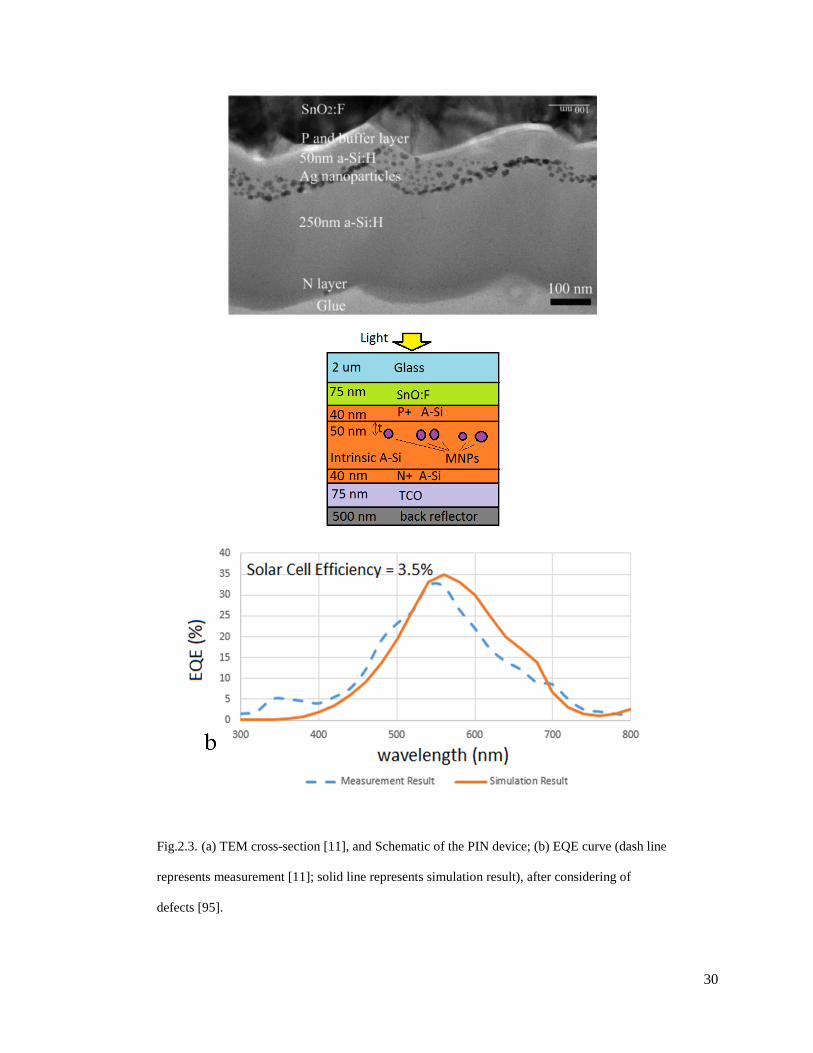
30
Fig.2.3. (a) TEM cross-section [11], and Schematic of the PIN device; (b) EQE curve (dash line
represents measurement [11]; solid line represents simulation result), after considering of
defects [95].
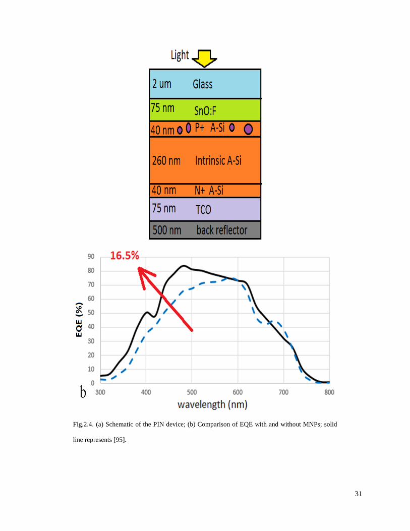
31
Fig.2.4. (a) Schematic of the PIN device; (b) Comparison of EQE with and without MNPs; solid
line represents [95].
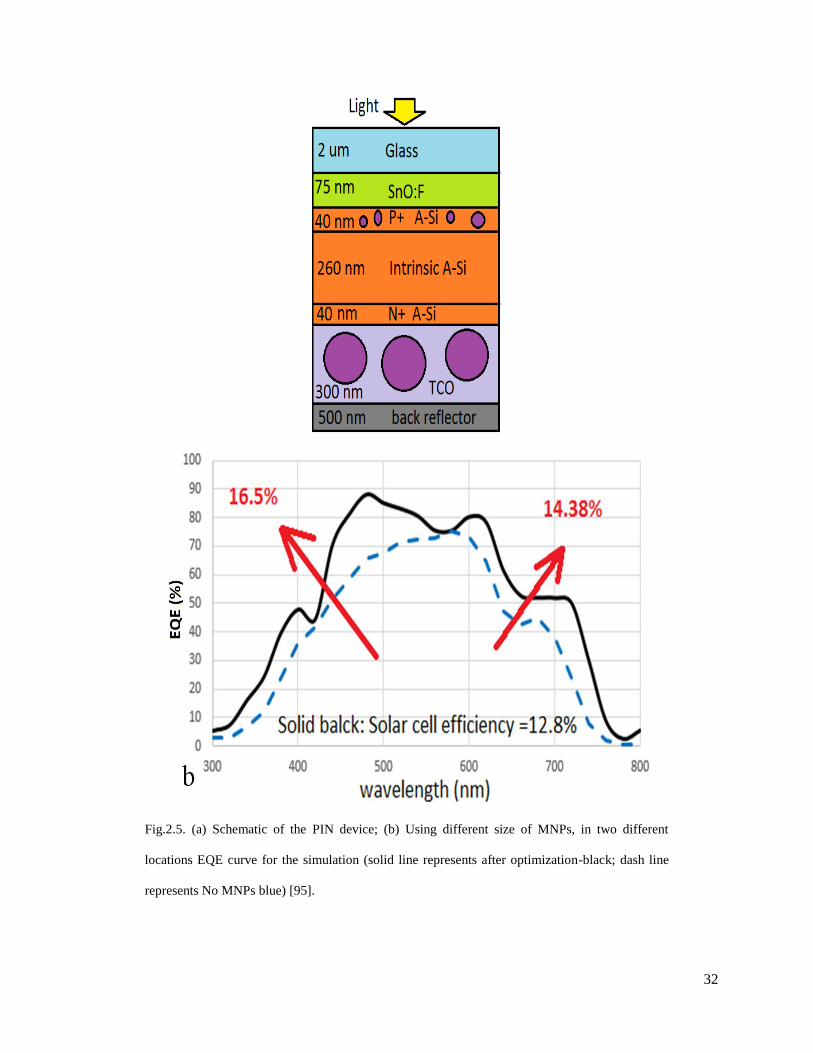
32
Fig.2.5. (a) Schematic of the PIN device; (b) Using different size of MNPs, in two different
locations EQE curve for the simulation (solid line represents after optimization-black; dash line
represents No MNPs blue) [95].

33
2.4. Optimization of highly doped regions
Another parameter that can impact the efficiency of solar cell is the layer thickness. At high frequencies
(UV region), most of the impinging solar energy on the cell is absorbed at the top of the semiconductor
(here P+ region) before approaching the depletion region. This is translated to an energy loss [18-21].
However, if light instead of being absorbed mostly in the P+ layers and free carries are recombined in the
same layer, is directed to the depletion region and propagates in a longer path inside it, more electron-hole
pairs would be created and kept separate as recombination rate is proportional to carrier doping density. It
was mentioned before that light with higher frequencies (UV) is not capable of reaching to the depletion
region. This would require: first, optimizing the thickness of the highly doped layer; and second, optimizing
the amount of dopant. Hence, the thickness of P+ layer should be thinned and the dopant (here P+) level
needs to be decreased, thus pushing the depletion region closer to the top. Thus, the probability of creating
electron hole pairs for UV increases significantly and would stay free. Moreover, even small MNPs can be
embedded between the electrode and semiconductor on the top layer side, instead of the P+ region for ease
of fabrication. And in this case, the near field of those nanoparticles (at resonance) would still affect the
depletion region and could still generate more free electron-hole pairs compared to embedding MNPs on
the P+ layer.
2.5. Conclusion
Random embedding of MNPs has resulted in an unexpected degradation of solar cell efficiency.
Extensive simulation, based on our 3D modeling Toolbox has led to very promising results. First, a
significant efficiency drop after adding the MNPs has been related to the substantial number of defects
left after embedding. Presence of these defects has resulted in a considerable optical loss around the
MNPs.
Second, a pronounced increase in recombination rates (if generated free electron-hole pairs were kept at
the highly doped region) which would reduce the conversion of optical energy to photons. Hence, better
manufacturing techniques need to be developed to reduce such defects, reduce recombination, and direct

34
more light to the intrinsic region. Such as strategically locating these MNPs at the highly populated
regions (i.e. P+ and N+) rather than in the intrinsic layer to help in achieving a significant drop in
recombination rates.
Additionally, using small MNPs at the top (P+) layer, should allow a significant portion of the optical
energy to propagate through (it acts like a transparent layer for lower frequencies), meanwhile larger
MNPs are placed at the bottom to enhance reflection/scattering. It is certainly not recommended to embed
those large MNPs inside the active region, because it can create a large amount of optical loss for the
whole system. Simulations indicated an impressive efficiency enhancement of up to ~30% which amount
to 12.8% overall efficiency.
2.6. Appendix theories
To calculate the intensity of light inside the structure, Maxwell’s equations are required. For general
time-varying fields, Maxwell’s equations are
∇ × 𝐻 = 𝐽 +𝜕𝐷
𝜕𝑡 (Eq.2.1)
∇ × 𝐸 = −𝜕𝐵
𝜕𝑡 (Eq.2.2)
∇ ∙ 𝐷 = 𝜌 (Eq.2.3)
∇ ∙ 𝐵 = 0 (Eq.2.4)
The quantities used in these equations are: Electric field intensity E, Electric displacement or electric flux
density D, Magnetic field intensity H, Magnetic flux density B, Current density J, and Electric charge
density ρ. The solver solves these equations in frequency domain. The time harmonic form of the Maxwell’s
equations are shown in below when the excitation is of the sinusoidal type.
𝐸(𝑥, 𝑦, 𝑧, 𝑡) = 𝐸(𝑥, 𝑦, 𝑧)𝑒𝑗𝜔𝑡 (Eq.2.5)
𝐻(𝑥, 𝑦, 𝑧, 𝑡) = 𝐻(𝑥, 𝑦, 𝑧)𝑒𝑗𝜔𝑡 (Eq.2.6)
After combining the time harmonic equations, we can describe electromagnetic wave propagation inside
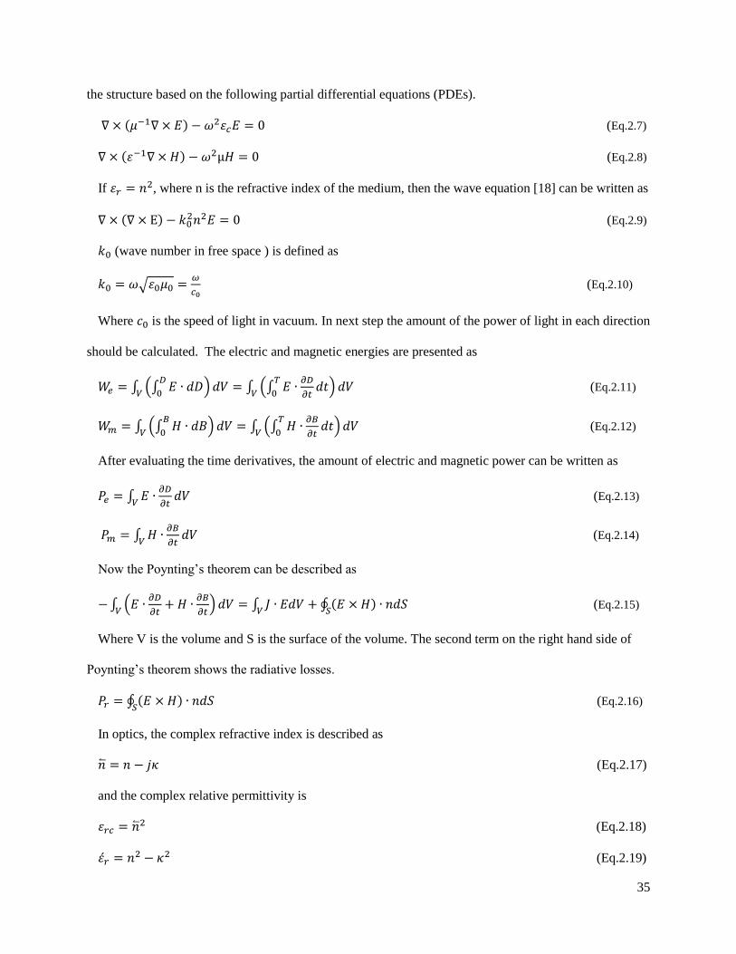
35
the structure based on the following partial differential equations (PDEs).
∇ × (𝜇−1∇ × 𝐸) − 𝜔2𝜀𝑐𝐸 = 0 (Eq.2.7)
∇ × (𝜀−1∇ × 𝐻) − 𝜔2µ𝐻 = 0 (Eq.2.8)
If 𝜀𝑟 = 𝑛2, where n is the refractive index of the medium, then the wave equation [18] can be written as
∇ × (∇ × E) − 𝑘02𝑛2𝐸 = 0 (Eq.2.9)
𝑘0 (wave number in free space ) is defined as
𝑘0 = 𝜔√𝜀0𝜇0 =𝜔
𝑐0 (Eq.2.10)
Where 𝑐0 is the speed of light in vacuum. In next step the amount of the power of light in each direction
should be calculated. The electric and magnetic energies are presented as
𝑊𝑒 = ∫ (∫ 𝐸 ∙ 𝑑𝐷𝐷
0) 𝑑𝑉 = ∫ (∫ 𝐸 ∙
𝜕𝐷
𝜕𝑡
𝑇
0𝑑𝑡) 𝑑𝑉
𝑉
𝑉 (Eq.2.11)
𝑊𝑚 = ∫ (∫ 𝐻 ∙ 𝑑𝐵𝐵
0) 𝑑𝑉 = ∫ (∫ 𝐻 ∙
𝜕𝐵
𝜕𝑡
𝑇
0𝑑𝑡) 𝑑𝑉
𝑉
𝑉 (Eq.2.12)
After evaluating the time derivatives, the amount of electric and magnetic power can be written as
𝑃𝑒 = ∫ 𝐸 ∙𝜕𝐷
𝜕𝑡𝑑𝑉
𝑉 (Eq.2.13)
𝑃𝑚 = ∫ 𝐻 ∙𝜕𝐵
𝜕𝑡𝑑𝑉
𝑉 (Eq.2.14)
Now the Poynting’s theorem can be described as
−∫ (𝐸 ∙𝜕𝐷
𝜕𝑡+ 𝐻 ∙
𝜕𝐵
𝜕𝑡) 𝑑𝑉 = ∫ 𝐽 ∙ 𝐸𝑑𝑉 + ∮ (𝐸 × 𝐻) ∙ 𝑛𝑑𝑆
𝑆
𝑉
𝑉 (Eq.2.15)
Where V is the volume and S is the surface of the volume. The second term on the right hand side of
Poynting’s theorem shows the radiative losses.
𝑃𝑟 = ∮ (𝐸 × 𝐻) ∙ 𝑛𝑑𝑆
𝑆 (Eq.2.16)
In optics, the complex refractive index is described as
�� = 𝑛 − 𝑗𝜅 (Eq.2.17)
and the complex relative permittivity is
𝜀𝑟𝑐 = ��2 (Eq.2.18)
𝜀�� = 𝑛2 − 𝜅2 (Eq.2.19)
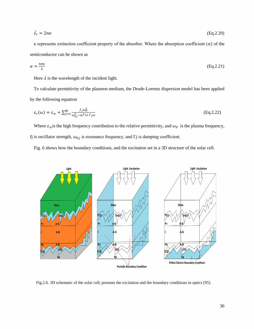
36
𝜀�� = 2𝑛𝜅 (Eq.2.20)
κ represents extinction coefficient property of the absorber. Where the absorption coefficient (𝛼) of the
semiconductor can be shown as
𝛼 =4𝜋𝜅
𝜆 (Eq.2.21)
Here 𝜆 is the wavelength of the incident light.
To calculate permittivity of the plasmon medium, the Drude-Lorentz dispersion model has been applied
by the following equation
𝜀𝑟(𝜔) = 𝜀∞ + ∑𝑓𝑗𝜔𝑃
2
𝜔0𝑗2 −𝜔2+𝑖 𝛤𝑗𝜔
𝑀𝑗=1 (Eq.2.22)
Where 𝜀∞is the high frequency contribution to the relative permittivity, and 𝜔𝑃 is the plasma frequency,
fj is oscillator strength, 𝜔0𝑗 is resonance frequency, and Γj is damping coefficient.
Fig. 6 shows how the boundary conditions, and the excitation set in a 3D structure of the solar cell.
Fig.2.6. 3D schematic of the solar cell; presents the excitation and the boundary conditions in optics [95].
37
If 𝐼𝑓 is defined as vector of the initial light power intensity in frequency domain, (for whole structure),
this vector can be shown in three directions.
𝐼𝑓 (𝑥, 𝑦, 𝑧) = 𝐼𝑓𝑥(𝑥, 𝑦, 𝑧)𝑥 + 𝐼𝑓𝑦(𝑥, 𝑦, 𝑧)�� + 𝐼𝑓𝑧(𝑥, 𝑦, 𝑧)�� (Eq.2.23)
After differentiating in space, and considering the amount of light absorption (𝛼 in frequency domain),
then the new PDE [19] is presented.
𝜕𝐼𝑓𝑥(𝑥,𝑦,𝑧)
𝜕𝑥𝑥 +
𝜕𝐼𝑓𝑦(𝑥,𝑦,𝑧)
𝜕𝑦�� +
𝜕𝐼𝑓𝑧(𝑥,𝑦,𝑧)
𝜕𝑧�� = −𝛼𝐼𝑓 (𝑥, 𝑦, 𝑧) (Eq.2.24)
Final step in optics is to extract the amount of light energy absorbed only inside the absorber (i.e.
semiconductor), and translate it to the generation rate of electron hole pairs G [19]. (Given by (Eq.2.25))
𝐺(𝑥, 𝑦, 𝑧) =𝛼(√𝐼𝑓𝑥
(𝑥,𝑦,𝑧)2+𝐼𝑓𝑦(𝑥,𝑦,𝑧)2+𝐼𝑓𝑧
(𝑥,𝑦,𝑧)2)
ℎ𝑛 (Eq.2.25)
To calculate the amount of minority carriers (electron and hole) inside the semiconductor, the transport
of diluted species are solved [19-21]. All equations (26-30) are presented only for the electron minority
carriers.
∇ ∙ 𝐽𝑛 − 𝑞𝜕𝑛
𝜕𝑡− 𝑞
𝜕𝜌𝑛
𝜕𝑡= q𝑅𝑡(𝑥, 𝑦, 𝑧) (Eq.2.26)
Where 𝑅𝑡(𝑥, 𝑦, 𝑧) is defined as the total rate of changing electron hole pairs inside the system.
𝜕𝐽𝑛𝑥
𝜕𝑥+
𝜕𝐽𝑛𝑦
𝜕𝑦+
𝜕𝐽𝑛𝑧
𝜕𝑧− 𝑞
𝜕𝑛
𝜕𝑡− 𝑞
𝜕𝜌𝑛
𝜕𝑡= q𝑅𝑡(𝑥, 𝑦, 𝑧) (Eq.2.27)
𝐽𝑛 = 𝐽𝑛𝑥 + 𝐽𝑛𝑦
+ 𝐽𝑛𝑧 (Eq.2.28)
𝐽𝑛 = (−𝑞𝑛𝜇𝑛𝜕𝜑
𝜕𝑥+ 𝑞𝐷𝑛𝑥
𝜕𝑛
𝜕𝑥) 𝑥 + (−𝑞𝑛𝜇𝑛
𝜕𝜑
𝜕𝑦+ 𝑞𝐷𝑛𝑦
𝜕𝑛
𝜕𝑦) 𝑦 + (−𝑞𝑛𝜇𝑛
𝜕𝜑
𝜕𝑧+ 𝑞𝐷𝑛𝑧
𝜕𝑛
𝜕𝑧) 𝑧 (Eq.2.29)
The continuity equation [19-21] for electron minority carriers can be written as
−𝑛𝜇𝑛 (−𝑞
𝜀(𝑝 − 𝑛 + 𝑐)) + 𝐷𝑛𝑥
𝜕2𝑛
𝜕𝑥2 + 𝐷𝑛𝑦𝜕2𝑛
𝜕𝑦2 + 𝐷𝑛𝑧𝜕2𝑛
𝜕𝑧2 + (−1 +𝑞
𝜀)
𝜕𝑛
𝜕𝑡= 𝑅𝑡(𝑥, 𝑦, 𝑧) (Eq.2.30)
𝑅𝑡(𝑥, 𝑦, 𝑧) = 𝐺(𝑥, 𝑦, 𝑧) − 𝑅(𝑥, 𝑦, 𝑧) (Eq.2.31)
Where 𝑅(𝑥, 𝑦, 𝑧) is defined as the Shockley Read Hall recombination rate (32-36) [22-23].
38
To extract the amount of 𝑅(𝑥, 𝑦, 𝑧)equations (32-36) [22-23] need to be calculated as well.
∆𝐸𝑡 = 𝐸𝑡 − 𝐸𝑖 (Eq.2.32)
𝑛1 = 𝛾𝑛√𝑁𝑐𝑁𝑣𝑒𝑥𝑝 (−𝐸𝑔−∆𝐸𝑔
2𝑉𝑡ℎ) 𝑒𝑥𝑝 (
∆𝐸𝑡
𝑉𝑡ℎ) (Eq.2.33)
𝑝1 = 𝛾𝑝√𝑁𝑐𝑁𝑣𝑒𝑥𝑝 (−𝐸𝑔−∆𝐸𝑔
2𝑉𝑡ℎ) 𝑒𝑥𝑝 (
∆𝐸𝑡
𝑉𝑡ℎ) (Eq.2.34)
𝑛𝑖 = 𝛾𝑛𝛾𝑝√𝑁𝑐𝑁𝑣𝑒𝑥𝑝 (−𝐸𝑔−∆𝐸𝑔
2𝑉𝑡ℎ) (Eq.2.35)
𝑅(𝑥, 𝑦, 𝑧) = 𝑅𝑛(𝑥, 𝑦, 𝑧) = 𝑅𝑃(𝑥, 𝑦, 𝑧) =𝑛𝑝−𝑛𝑖
2
𝜏𝑝(𝑛1+𝑛)𝜏𝑛(𝑝1+𝑝) (Eq.2.36)
Where φ (Electric Potential), p (Hole concentration), and n (Electron concentration) are variables, q
(Electron charge), ε (Optical property of the material), c (Initial value for carrier concentration), 𝑛𝑖 (intrinsic
concentration), 𝜏𝑛 (Electron life time), 𝜏𝑝 (Hole life time), α (absorption coefficient of material), 𝜇𝑛
(Electron mobility), 𝜇𝑝 (Hole mobility), and 𝐷𝑛 (Electron Diffusivity) are constants. Also 𝛾𝑛 and 𝛾𝑝 are
the electron and hole degeneracy factors, 𝑁𝑐 and 𝑁𝑣 are the effective densities of states for the conduction
and valence band, 𝐸𝑔 is the band-gap and ∆𝐸𝑔 the band gap narrowing. 𝐸𝑡 is the trap energy level. Energy
difference between the defect level and the intrinsic level is ∆𝐸𝑡.The same equations should be derived for
holes. The value of each parameter is shown in Table. 2.1.
Finally to find voltage-current relationship of the solar cell, the amount of minority carriers at both sides
of the semiconductor should be found, based on Poisson’s equation at each electrodes.
Here space charge density (Electron) is
𝜌𝑛 = −𝑞
𝜀𝑛 (Eq.2.37)
The Poisson’s Equation [19-21] can be written as
�� . �� 𝜑 = −𝑞
𝜀(𝑝 − 𝑛 + 𝑐) (Eq.2.38)
𝜕2𝜑
𝜕𝑥2 +𝜕2𝜑
𝜕𝑦2 +𝜕2𝜑
𝜕𝑧2 = −𝑞
𝜀(𝑝 − 𝑛 + 𝑐) (Eq.2.39)

39
Throughout the whole process, the PDEs are solved in steady state; transient solutions are not considered
(∂n/∂t=0 or ∂p/∂t=0). The excess minority carrier concentration increases with time. The excess carrier
concentration reaches a steady-state value as time goes to infinity, even though a steady-state generation of
excess electrons and hole exists [19]. The generation rate G is a function of wavelength and time. However,
we are only solving for steady state and ignore any time dependence. Wavelength dependence is often
included by summing the results obtained at one wavelength over all wavelengths of interest.
To solve this model in different physics, Free Tetrahedral has been chosen as a type of mesh. The
minimum element size in case of using MNPs is 1nm, and the maximum element size depends on the size
of the cell. (100nm is chosen here). The cad tool is used Finite Element Method (FEM) to solve the
nonlinear PDEs.

40
Table. 2.1 The utilized value of each parameter
T(temperature) 300[K]
Ni -Ref[29] 0.949E6 [cm-3]
Doping (N+) 1E20[cm-3]
Doping (P+) 1E21[cm-3]
Thickness (N+, a-Si)-Ref [11] 40 [nm]
Thickness (intrinsic, a-Si)- Ref [11] 260 [nm]
Thickness (P+, a-Si)- Ref [11] 40 [nm]
Thickness (AZO) -( TCO in front)- Ref [11] 75[nm]
Thickness -(TCO BACK)- Ref [11] 75[nm](AZO)
Thickness (Silver) Reflector back- Ref [11] 500[nm]
Electron mobility, a-Si -intrinsic-Ref [29] 20[cm2/( V s)]
Hole mobility, a-Si -intrinsic-Ref [29] 2[cm2/( V s)]
Electron mobility, a-Si N+-Ref [29] 20[cm2/( V s)]
Hole mobility, a-Si N+-Ref [29] 2[cm2/( V s)]
Electron mobility, a-Si P+-Ref [29] 20[cm2/( V s)]
Hole mobility, a-Si P+-Ref[29] 2[cm2/(V s)]
Electron Life time, a-Si -intrinsic-Ref [30, 28] 20[ns]
Hole Life time, a-Si -intrinsic-Ref [30, 28] 20[ns]
Electron Life time, a-Si N+-Ref [30, 28] 0.0001[ns]
Hole Life time, a-Si N+-Ref [30, 28] 10[ns]
Electron Life time, a-Si P+-Ref [31,32] 10[ns]
Hole Life time, a-Si P+-Ref [21,32] 0.0001[ns]
Density Of State Valence band, a-Si –Ref [33] 2.5E20[cm-3]
Density Of State Conduction band, a-Si –Ref [33] 2.5E20[cm-3]
Difference between Defect level and intrinsic level N+,P+-Ref [20] 0.7
Difference between Defect level and intrinsic level intrinsic-Ref [20] 0.3
Energy Band gap a-Si-Ref [28] 1.74
diameter silver NPs-Ref [11] 20[nm]
Affinity, a-Si (electro affinity)-Ref [29] 4.00eV
Incident Light Angle 0 [deg]
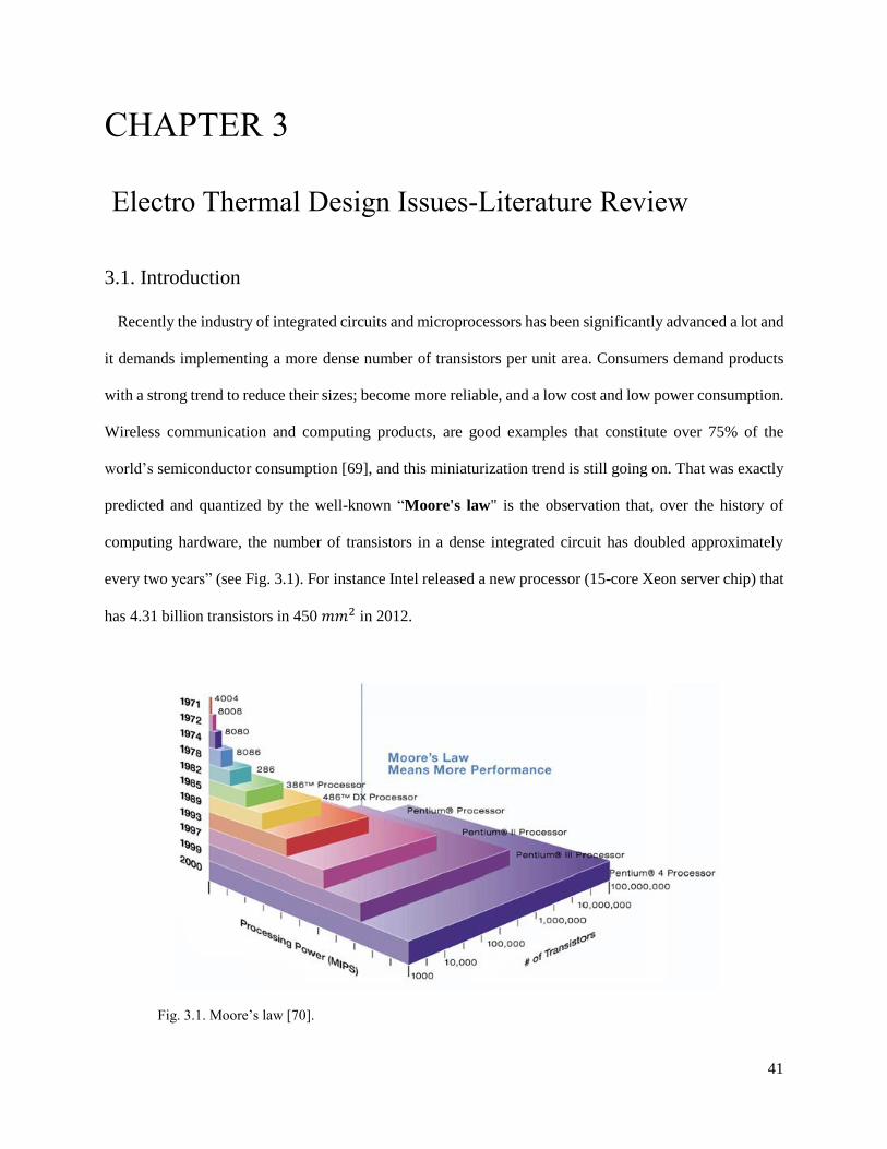
41
CHAPTER 3
Electro Thermal Design Issues-Literature Review
3.1. Introduction
Recently the industry of integrated circuits and microprocessors has been significantly advanced a lot and
it demands implementing a more dense number of transistors per unit area. Consumers demand products
with a strong trend to reduce their sizes; become more reliable, and a low cost and low power consumption.
Wireless communication and computing products, are good examples that constitute over 75% of the
world’s semiconductor consumption [69], and this miniaturization trend is still going on. That was exactly
predicted and quantized by the well-known “Moore's law" is the observation that, over the history of
computing hardware, the number of transistors in a dense integrated circuit has doubled approximately
every two years” (see Fig. 3.1). For instance Intel released a new processor (15-core Xeon server chip) that
has 4.31 billion transistors in 450 𝑚𝑚2 in 2012.
Fig. 3.1. Moore’s law [70].
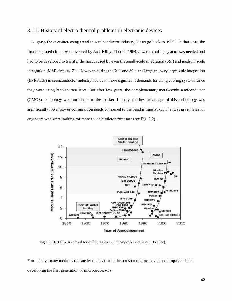
42
3.1.1. History of electro thermal problems in electronic devices
To grasp the ever-increasing trend in semiconductor industry, let us go back to 1959. In that year, the
first integrated circuit was invented by Jack Kilby. Then in 1964, a water-cooling system was needed and
had to be developed to transfer the heat caused by even the small-scale integration (SSI) and medium scale
integration (MSI) circuits [71]. However, during the 70’s and 80’s, the large and very large scale integration
(LSI/VLSI) in semiconductor industry had even more significant demands for using cooling systems since
they were using bipolar transistors. But after few years, the complementary metal-oxide semiconductor
(CMOS) technology was introduced to the market. Luckily, the best advantage of this technology was
significantly lower power consumption needs compared to the bipolar transistors. That was great news for
engineers who were looking for more reliable microprocessors (see Fig. 3.2).
Fig.3.2. Heat flux generated for different types of microprocessors since 1959 [72].
Fortunately, many methods to transfer the heat from the hot spot regions have been proposed since
developing the first generation of microprocessors.

43
Fig.3.3.Cooling system was designed for the 3081 computer [73].
Fig.3.4. Improvement in water-cooling systems for IBM processors [73].

44
A very successful cooling example is the method developed for the 3081 computer, and is shown in Fig.
3.3—the heatsink in this case is made of Aluminum. Fig. 3.4 shows some cooling systems that were
invented for IBM processors (3081, ES/3090, and ES/9000). Alternatively, a water-cooling system was
developed for the power section of the Mac G5 computer and is shown in Fig. 3.5.
Recently, engineers have been working on microfluidic channels defined Through Silicon VIAs
“TSVs” to transfer the heat generated by many transistors (see Fig. 3.6) [91] to the heatsink.
Fig.3.5. Water-cooling machine for the Mac G5 computer [73].
As shown in Fig. 3.6, engineers who developed this system used very thick VIAs TSVs (for power) and
Ground TSVs (to handle large amount of current density). The whole structure is divided into several active
regions and the microfluidic channels are placed in between. In the new thermal designs, a very thin film
of thermal glue material-Thermal Interface Material layer (TIM) is placed between the device and the body
of the heatsink. It has been demonstrated that the use of TIM is very effective in transferring the heat
successfully. Additionally, by applying air convection cooling system, the heatsink gets cooler. In Fig. 3.7,
a high-speed fan is shown that is placed on top of the heatsink to circulate air as well.
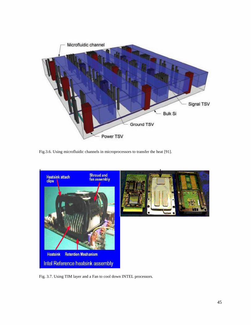
45
Fig.3.6. Using microfluidic channels in microprocessors to transfer the heat [91].
Fig. 3.7. Using TIM layer and a Fan to cool down INTEL processors.
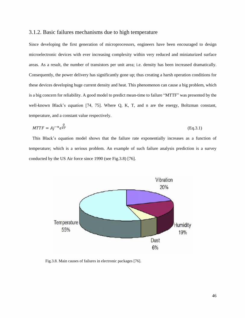
46
3.1.2. Basic failures mechanisms due to high temperature
Since developing the first generation of microprocessors, engineers have been encouraged to design
microelectronic devices with ever increasing complexity within very reduced and miniaturized surface
areas. As a result, the number of transistors per unit area; i.e. density has been increased dramatically.
Consequently, the power delivery has significantly gone up; thus creating a harsh operation conditions for
these devices developing huge current density and heat. This phenomenon can cause a big problem, which
is a big concern for reliability. A good model to predict mean-time to failure “MTTF” was presented by the
well-known Black’s equation [74, 75]. Where Q, K, T, and n are the energy, Boltzman constant,
temperature, and a constant value respectively.
𝑀𝑇𝑇𝐹 = 𝐴𝑗−𝑛𝑒𝑄
𝐾𝑇 (Eq.3.1)
This Black’s equation model shows that the failure rate exponentially increases as a function of
temperature; which is a serious problem. An example of such failure analysis prediction is a survey
conducted by the US Air force since 1990 (see Fig.3.8) [76].
Fig.3.8. Main causes of failures in electronic packages [76].

47
Fig. 3.8 shows that 55% of all electronic circuits failures is due to hot spot regions created inside the
packages, while only 5% due to dust, 19% due to humidity and 20% due to vibration. For instance, in a
very tiny region of interconnects, raising the temperature due to high power delivery can significantly
lead to physical shape deformation of the metallic traces or VIAs. It has been demonstrated also that the
current density at critical regions (from the pad to the bump- for example) typically goes up after a given
temperature cycles (this phenomena is known as the current crowding). Due to both the high power
delivery and current crowding huge movement of electrons from one side to the other in a tiny region
causes electro-migration [77 and 78]. This phenomenon creates cracks in interconnector’s metallization.
Fig. 3.9 shows clearly a defect caused by this electro-migration phenomenon [67]. This scenario is really
getting worse, as there is a trend to minimize these copper bumps, hence it is a must in current designs to
validate the current density in all traces to avoid electro-migration effects. Fig. 3.10 shows that the current
density obviously increases upon using a smaller bump [69]. It is expected, of course, for a smaller bump,
more defects could happen based on electro-migration. Typically, the material properties of the plastic
package of all components including the microprocessors, power amplifiers, power transistors, and chips
affect the lifetime. Fig. 3.11 shows that some cracks that happened due to heat or mechanical stresses on
plastic packages, however further studies are still needed to minimize thermal deformation or expansion,
to develop new techniques to transfer more heat to the heatsink (see Fig. 3.12) more efficiently.
Additionally, several studies have shown that the electro-migration lifetime is a function of both the width
of the traces [86 and 87] and the size of grains. Research is still underway to develop better heat
protection techniques [88]. Another problem that is currently being investigated by mechanical engineers
is studying the mechanical stress impact around the copper pillars and significant advancements have
been made. For instance, a special material with low expansion has been invented to protect the copper
pillar from mechanical stress and heat. In other words, by using this new material, the chip reliability can
be significantly increased at high temperature [90] (see Fig. 3.13). Additionally in the last two decades,
for example, engineers were able to design and fabricate arrays of small bumps for many applications
[79-84] (see Fig. 3.14). In Table. 3.1 Different failure classifications and mechanisms are listed [69].
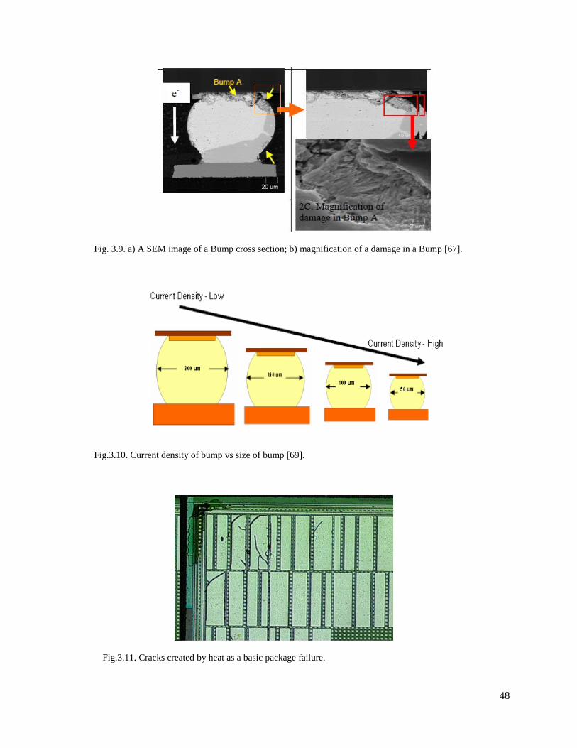
48
Fig. 3.9. a) A SEM image of a Bump cross section; b) magnification of a damage in a Bump [67].
Fig.3.10. Current density of bump vs size of bump [69].
Fig.3.11. Cracks created by heat as a basic package failure.

49
Fig.3.12. Flip-chip package with copper heat sink [89].
Fig.3.13. Single copper pillar system supported by a polymer [90].
Fig.3.14. Flip chip ball grid array (a) Front; (b) back side; (c) SEM of copper pillar bumps. (d)
Magnified copper pillar bumps [85].

50
Table.3.1 (a). Failure classifications and mechanisms are listed (after [69]).
Basic failure
mechanisms
# Failure origins and driving forces Failure examples Fault isolation and failure analysis
methods
A: Coherent
crack
formation
1 Thermo-mechanical mismatch Chip solder fatigue
BGA solder ball fatigue
Fracture of an embedded passive
component
Die-to-die spacer crack
Underfill crack
IC metal line open
Stress analysis: by Thermoire-
Interferometry, Speckle Interferometry (ESPI), Deformation analysis by image
correlation, x-ray diffraction
Fault isolation: by Magnetic microscopy,
Time domain reflectance, Lock in
thermography, TIVA, OBIRCH
Crack detection: by Scanning Acoustic
Microscopy, Cross section analysis with light microscopy, SEM or FIB/SEM
A 2 Mechanical loading (application
or
process-induced)
IC dielectric crack Organic
substrate crack
Solder ball crack (drop)
A 3 Hygroscopic swelling Mold compound cracking, die
cracking, substrate cracking
A 4 Reaction-induced volume shrink
or expansion (e.g. curing)
Mold compound cracking, die
cracking
A 5 Internal pressure (e.g. moisture
vaporization at increased
temperature)
Mold compound cracking, die
cracking
B: Interfacial
delamination
1-5 Same as 1-5 IC dielectric delamination
Underfill delamination
Delamination between stacked
dies Organic substrate
delamination
Mold compound delamination
Stress analysis: by Thermoire-
Interferometry,
Speckle-Interferometry (ESPI), Deformation analysis by image
correlation, x-ray diffraction
Crack detection: by Scanning Acoustic
Microscopy, Cross section analysis with
light microscopy or SEM, FIB/SEM, FIB/TEM
B 6 Interface reactions causing loss
of adhesion (e.g. moisture-,
oxidation-, contamination-related)
Underfill delamination
Mold compound delamination
Organic substrate delamination
Crack detection: by Scanning Acoustic
Microscopy, Cross section analysis with
light microscopy or SEM, FIB/SEM, FIB/TEM
Surface analysis: by TOF-SIMS, XPS,
AES, TEM+EDX, TEM+EELS

51
Table.3.1 (b). Failure classifications and mechanisms are listed (after [69]).
Basic failure
mechanisms
# Failure origins and driving forces Failure examples Fault isolation and failure analysis
methods
C: Void and
pore
formation
7 Mechanical creep IC Solder ball fatigue
BGA solder ball fatigue
Fault isolation: by Magnetic microscopy,
Time domain reflectance, Lock in thermography,
TIVA, OBIRCH
Void detection: by x-ray microscopy or
x-ray tomography Cross section analysis
with light microscopy, SEM or FIB/SEM (with EDX,WDX, EBSD and x-ray
diffraction for analysis of intermetallic)
C 8 Diffusion (Kirkendall void
formation) and Intermetallic
formation
IC UBM lift
Void in IC interconnect or in
via
Wire bond lift
BGA solder ball lift
C 9 Electro migration Void in IC metal line or
solder, Void in solder, metal
line or via in the BGA
substrate
C 10 Thermomigration Void in IC metal line or
solder, Void in solder, metal
line or via in the BGA
substrate
D: Material
decomposition
and
bulk reactions
11 Chemical corrosion Bond wire lift Fault isolation: by Magnetic microscopy, Time domain reflectance, Lock in
thermography, TIVA, OBIRCH
Failure analysis: by Cross section
analysis with light microscopy or based
on FIB/SEM with EDX or WDX, TEM, TOF-SIMS, XPS, FTIR
spectroscopy, , mechanical testing, TGA,
DMA, DSC (ageing), EBSD (grain analysis)
D 12 Galvanic corrosion Bond wire lift
13 Ageing (UV, …) Organic substrate cracking
or delamination
Underfill cracking or
delamination
Crack detection: by Scanning Acoustic Microscopy, Cross section analysis with
light microscopy or SEM, FIB/SEM,
FIB/TEM Surface analysis: by TOF-SIMS, XPS,
AES, TEM+EDX, TEM+EELS
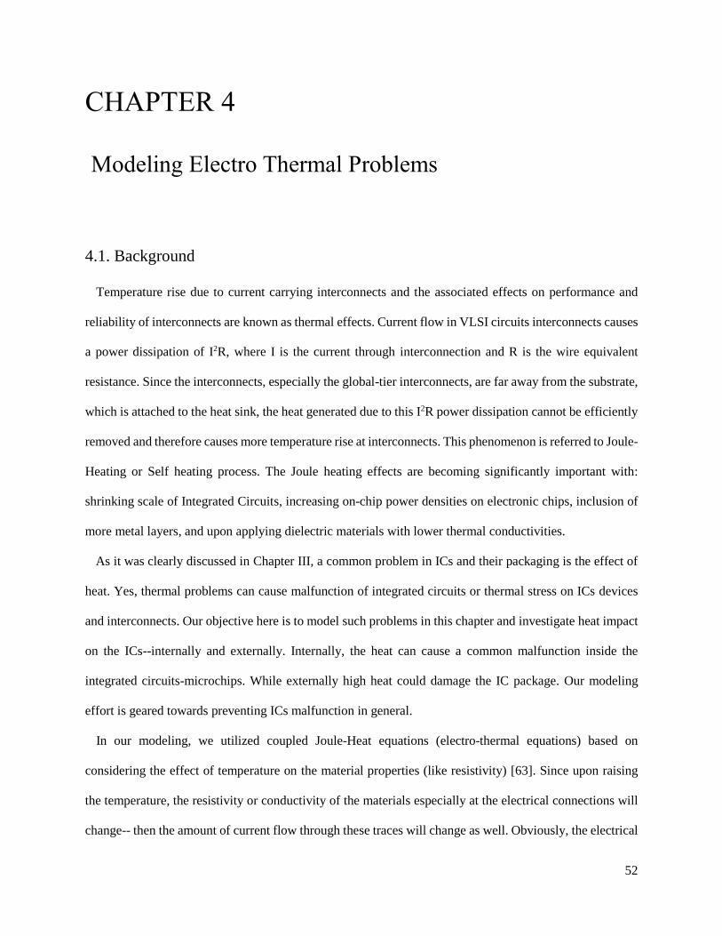
52
CHAPTER 4
Modeling Electro Thermal Problems
4.1. Background
Temperature rise due to current carrying interconnects and the associated effects on performance and
reliability of interconnects are known as thermal effects. Current flow in VLSI circuits interconnects causes
a power dissipation of I2R, where I is the current through interconnection and R is the wire equivalent
resistance. Since the interconnects, especially the global-tier interconnects, are far away from the substrate,
which is attached to the heat sink, the heat generated due to this I2R power dissipation cannot be efficiently
removed and therefore causes more temperature rise at interconnects. This phenomenon is referred to Joule-
Heating or Self heating process. The Joule heating effects are becoming significantly important with:
shrinking scale of Integrated Circuits, increasing on-chip power densities on electronic chips, inclusion of
more metal layers, and upon applying dielectric materials with lower thermal conductivities.
As it was clearly discussed in Chapter III, a common problem in ICs and their packaging is the effect of
heat. Yes, thermal problems can cause malfunction of integrated circuits or thermal stress on ICs devices
and interconnects. Our objective here is to model such problems in this chapter and investigate heat impact
on the ICs--internally and externally. Internally, the heat can cause a common malfunction inside the
integrated circuits-microchips. While externally high heat could damage the IC package. Our modeling
effort is geared towards preventing ICs malfunction in general.
In our modeling, we utilized coupled Joule-Heat equations (electro-thermal equations) based on
considering the effect of temperature on the material properties (like resistivity) [63]. Since upon raising
the temperature, the resistivity or conductivity of the materials especially at the electrical connections will
change-- then the amount of current flow through these traces will change as well. Obviously, the electrical

53
loss will be transformed to heat and change the temperature of the junctions, i.e. coupled physical process.
This phenomenon acts like a closed loop, but finally the whole system will be stable at one point.
The coupled Joule-Heating equations have been numerically solved here by using COMSOL (a
commercial multi-physics solver). Various mounting strategies aiming at preventing or minimizing
malfunctions of the electronic systems are proposed here and will be described in details.
In the following sections, we will address the recent progress in ICs design first and the trend to achieve
a denser fabrication strategy towards size reduction and increased functionally, then look at its impact on
ICs reliability.
4.1.1. Joule-heating modeling inside IC package
The huge demand to achieve progressively increasing complex integrated circuits (ICs) is hampered
always with the goal to simultaneously achieve ultrafast switching speeds as well. Integrating larger
number of transistors, increasing their functional density [49] typically slow down the device. This trend
has been addressed lately by developing a multi-stack chip technology. However, making electrical
interconnects among these multi-stack devices is progressively becoming more and more complicated and
has become a very challenging issue day after day. For some special cases, it’s required, for example, to
reduce the cross section of the utilized interconnects (wires) to further miniaturize the multi-stack packed
transistors. However, the size of the various chips and their density would lead to creation of longer
interconnects. This problem is really getting worse with the aggressive scaling used in VLSI technology
that requires longer wires and smaller wire pitch. This trend has caused an unacceptable interconnect delay
and really a key crucial point that hurdles the continuous improvement in developing higher and higher
dense ICs and processing speeds [50-53]. To illustrate this rapid increase of ICs density in the last few
years, we list the evolution of Intel commercial processors in Table. 4.1. Typically, for more wiring inside
the structure, the number of metal layers has grown significantly as obviously seen from the table.
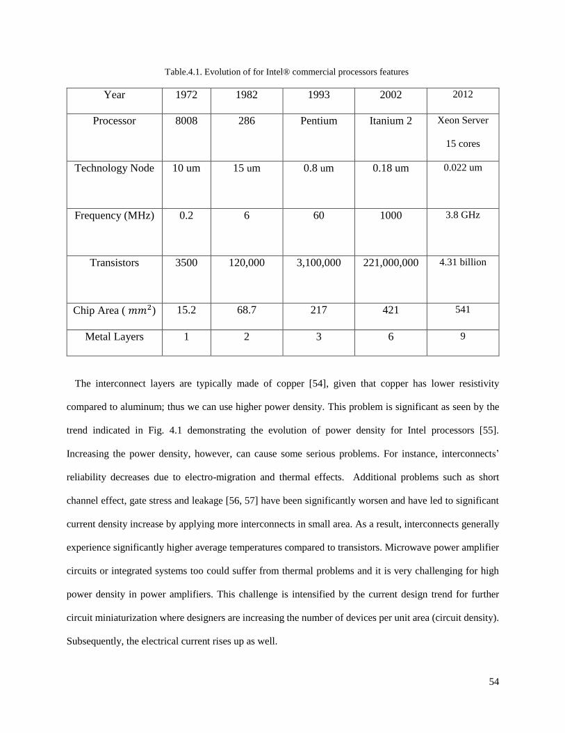
54
Table.4.1. Evolution of for Intel® commercial processors features
Year 1972 1982 1993 2002 2012
Processor 8008 286 Pentium Itanium 2 Xeon Server
15 cores
Technology Node 10 um 15 um 0.8 um 0.18 um 0.022 um
Frequency (MHz) 0.2 6 60 1000 3.8 GHz
Transistors 3500 120,000 3,100,000 221,000,000 4.31 billion
Chip Area ( 𝑚𝑚2) 15.2 68.7 217 421 541
Metal Layers 1 2 3 6 9
The interconnect layers are typically made of copper [54], given that copper has lower resistivity
compared to aluminum; thus we can use higher power density. This problem is significant as seen by the
trend indicated in Fig. 4.1 demonstrating the evolution of power density for Intel processors [55].
Increasing the power density, however, can cause some serious problems. For instance, interconnects’
reliability decreases due to electro-migration and thermal effects. Additional problems such as short
channel effect, gate stress and leakage [56, 57] have been significantly worsen and have led to significant
current density increase by applying more interconnects in small area. As a result, interconnects generally
experience significantly higher average temperatures compared to transistors. Microwave power amplifier
circuits or integrated systems too could suffer from thermal problems and it is very challenging for high
power density in power amplifiers. This challenge is intensified by the current design trend for further
circuit miniaturization where designers are increasing the number of devices per unit area (circuit density).
Subsequently, the electrical current rises up as well.
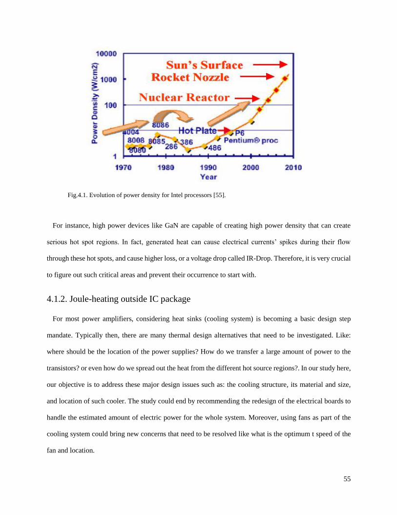
55
Fig.4.1. Evolution of power density for Intel processors [55].
For instance, high power devices like GaN are capable of creating high power density that can create
serious hot spot regions. In fact, generated heat can cause electrical currents’ spikes during their flow
through these hot spots, and cause higher loss, or a voltage drop called IR-Drop. Therefore, it is very crucial
to figure out such critical areas and prevent their occurrence to start with.
4.1.2. Joule-heating outside IC package
For most power amplifiers, considering heat sinks (cooling system) is becoming a basic design step
mandate. Typically then, there are many thermal design alternatives that need to be investigated. Like:
where should be the location of the power supplies? How do we transfer a large amount of power to the
transistors? or even how do we spread out the heat from the different hot source regions?. In our study here,
our objective is to address these major design issues such as: the cooling structure, its material and size,
and location of such cooler. The study could end by recommending the redesign of the electrical boards to
handle the estimated amount of electric power for the whole system. Moreover, using fans as part of the
cooling system could bring new concerns that need to be resolved like what is the optimum t speed of the
fan and location.
56
4.2. Basic analysis of electro-thermal problems
Nowadays by stacking multitude of chips on top of each other, the temperature of the whole system
typically goes up dramatically. For this reason many studies have been carried out to study the effect of
heat on the circuit performance, and to find a way to cool down any evolved hot spot region. In some cases,
designing power delivery network (PDN) is very crucial to decrease the IR drop in these hot spot regions.
Usually IR drop is considered when the material properties of the conductors are changed as a function
of temperature. For example, the material’s resistivity property will be higher at higher temperatures
compared to its normal value at room temperature. Thus IR drop increase is translated to an extra loss for
the PDN. The best way to check the reliability of PDN though is to use CAD tools to predict the steady
state value for the major parameters like: temperature and IR drop for the PDN especially these connections
in the PDNs that have significant high electrical resistance and would cause unacceptable IR drop. These
drops are function of temperature. Obviously, electrical and thermal fields are coupled, and an electrical-
thermal co-analysis is required which is a difficult task given that the thermal distribution is non-uniform
and hence the Joule-heating distribution across PDN and stacked chips is non-uniform.
Fortunately, during the last few years several numerical methods have been developed for the co-analysis
of these electro-thermal problems. These methods include: Green’s function method [92], finite element
method, and finite difference method [93] and many commercial CAD tools have been developed. In the
following, we will present our electro-thermal co-simulation analysis using COMSOL (a Multi-physics
commercial CAD tool-COMSOL 4.3).
In our analysis we will investigate different strategies to spread out the heat. Like using thermal VIAs to
minimize the electro-thermal problem in power amplifiers. Thermal VIAs are commonly used in either
silicon (TSV) or GaAs and they are key enablers when designing high-density 3D integrated systems. But,
for stacked chips in 3D systems, the heat flux density is high, and the thermal problem is still an
overwhelming challenging [58] and needs to be addressed. A brief background of these various thermal
issues were discussed in Chapter III and the challenge to solve them is listed here:
57
a) Hot spots in any power amplifier circuits can cause serious reliability problems.
b) Electrical current crowding in a daisy chain structure (especially between the pad trace and solder
bump) can cause serious failure [59-61].
c) Electrical current passing through a critical circuit node, where practically the current distribution
suddenly spikes, would generate more heat and subsequently more instability for the electron
mobility in the structure.
The thermal gradient could create significant thermo-migration [62]. Thermo-migration and electro-
migration accelerate this process for higher densities, this process could continue till the deformation
of the solder pillar occurs. This event causes a controversial failure for the electronic chips.
By coupling these electrical and thermal interdependences, we should be able to get accurate modeling
results that could help in better designing the heat sinks. Based on our extensive analysis, we will
develop a thermo-electric model of these devices and recommend potential ways to overcome such heat
issues later on.
4.2.1. Model development
The electrical equations that govern the steady state solution are given by Eq.4.1, where, the voltage
distribution in a power delivery system can be expressed as:
∇ ∙ (1
𝜌(𝑥,𝑦,𝑧,𝑇)∇φ(𝑥, 𝑦, 𝑧)) = 0 (Eq.4.1)
𝜑(𝑥, 𝑦, 𝑧) represents the electric potential distribution and 𝜌(𝑥, 𝑦, 𝑧, 𝑇) is the electric resistivity. While,
the electric resistivity is temperature-dependent, and is given by:
𝜌 = 𝜌0[1 + 𝛼(𝑇 − 𝑇0)] (Eq.4.2)
𝜌0 is the electric resistivity at 𝑇0 (assumed to be the room temperature 𝑜𝑓 20℃ ), and 𝛼 is the temperature
coefficient [63]. Also 𝑃(𝑥, 𝑦, 𝑧) is the heat created by the conductors’ loss and is expressed by:
𝑃(𝑥, 𝑦, 𝑧) = 𝐽 ∙ �� (𝑥, 𝑦, 𝑧) (Eq.4.3)
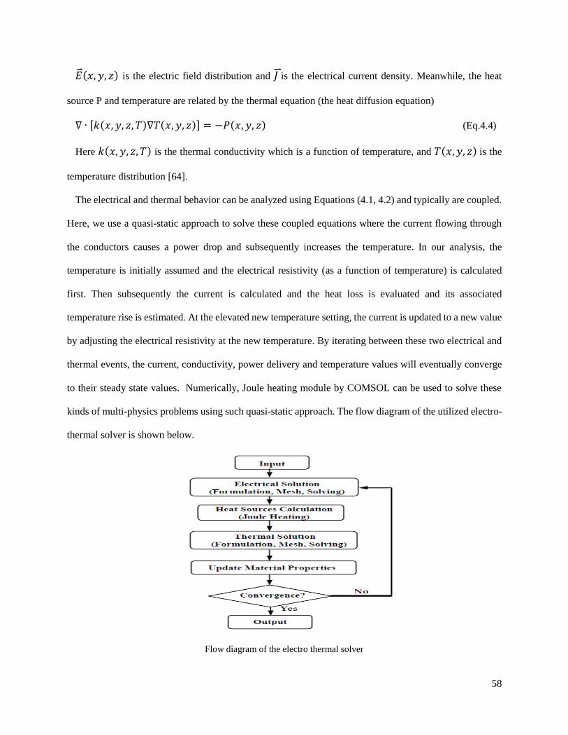
58
�� (𝑥, 𝑦, 𝑧) is the electric field distribution and 𝐽 is the electrical current density. Meanwhile, the heat
source P and temperature are related by the thermal equation (the heat diffusion equation)
∇ ∙ [𝑘(𝑥, 𝑦, 𝑧, 𝑇)∇𝑇(𝑥, 𝑦, 𝑧)] = −𝑃(𝑥, 𝑦, 𝑧) (Eq.4.4)
Here 𝑘(𝑥, 𝑦, 𝑧, 𝑇) is the thermal conductivity which is a function of temperature, and 𝑇(𝑥, 𝑦, 𝑧) is the
temperature distribution [64].
The electrical and thermal behavior can be analyzed using Equations (4.1, 4.2) and typically are coupled.
Here, we use a quasi-static approach to solve these coupled equations where the current flowing through
the conductors causes a power drop and subsequently increases the temperature. In our analysis, the
temperature is initially assumed and the electrical resistivity (as a function of temperature) is calculated
first. Then subsequently the current is calculated and the heat loss is evaluated and its associated
temperature rise is estimated. At the elevated new temperature setting, the current is updated to a new value
by adjusting the electrical resistivity at the new temperature. By iterating between these two electrical and
thermal events, the current, conductivity, power delivery and temperature values will eventually converge
to their steady state values. Numerically, Joule heating module by COMSOL can be used to solve these
kinds of multi-physics problems using such quasi-static approach. The flow diagram of the utilized electro-
thermal solver is shown below.
Flow diagram of the electro thermal solver

59
4.3. Electro-thermal simulation for devices at low frequency
4.3.1. Analysis of 3D electro-thermal simulations-3D integration system
In this section, a developed systematic method is used to analyze various 3D electro-thermal problems
and comparing simulated results to previously published experimental ones to validate our the method. In
this study, we analyze a 3D integrated system that includes two stacked chips (a memory chip stacked on
top of a CPU chip by using TSVs and controlled collapse chip connections C4s). This structure is comprised
of different parts (blocks) a power delivery network, a glass-ceramic substrate, through silicon VIAs (TSV),
controlled collapse chip connections (C4s), and a thermal interface material TIM (see Fig. 4.3).
As seen in Fig. 4.3, two metal layers are connected together through multiple-VIAs built through a glass
ceramic substrate (one layer at the top and another at the bottom of the ceramic substrate). The size of each
chip is 1.2 cm x 1.2 cm. The chips are fed by a 2.5 V voltage source located at the corner of this electronic
package as seen in Fig. 4.3. The power consumptions for the two chips (CPU, AND RAM) are 60 W, and
10 W respectively. The non-uniform power delivery is used to feed the 3D stacked integrated circuit listed
in Table.4.2.
Table.4.2 power consumption of the stacked chips [65] at 6 different regions indicated in Fig. 4.3
Chip#1 CPU#1 7W, 15W,15W,10W,6.5W,6.5W
Chip#2 RAM#1 1.6W,1.6W,1.6W,1.6W,1.6W,1.6W
Fig. 4.2 shows the power map of the stacked chips. Table 4.3 and Table 4.4 show the thickness of each
layer and also the thermal conductivity of the materials (applied for this example).
Fig.4.2. Electric power map for the stacked chips (a) CPU (b) RAM [65]
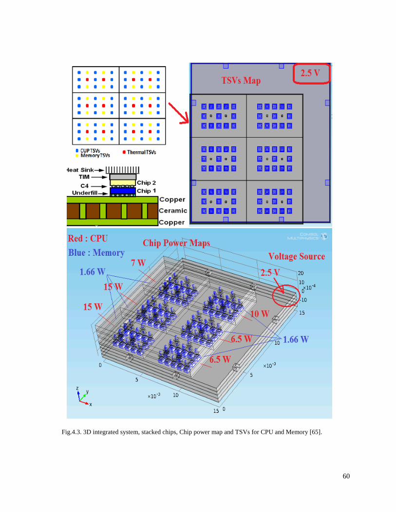
60
Fig.4.3. 3D integrated system, stacked chips, Chip power map and TSVs for CPU and Memory [65].
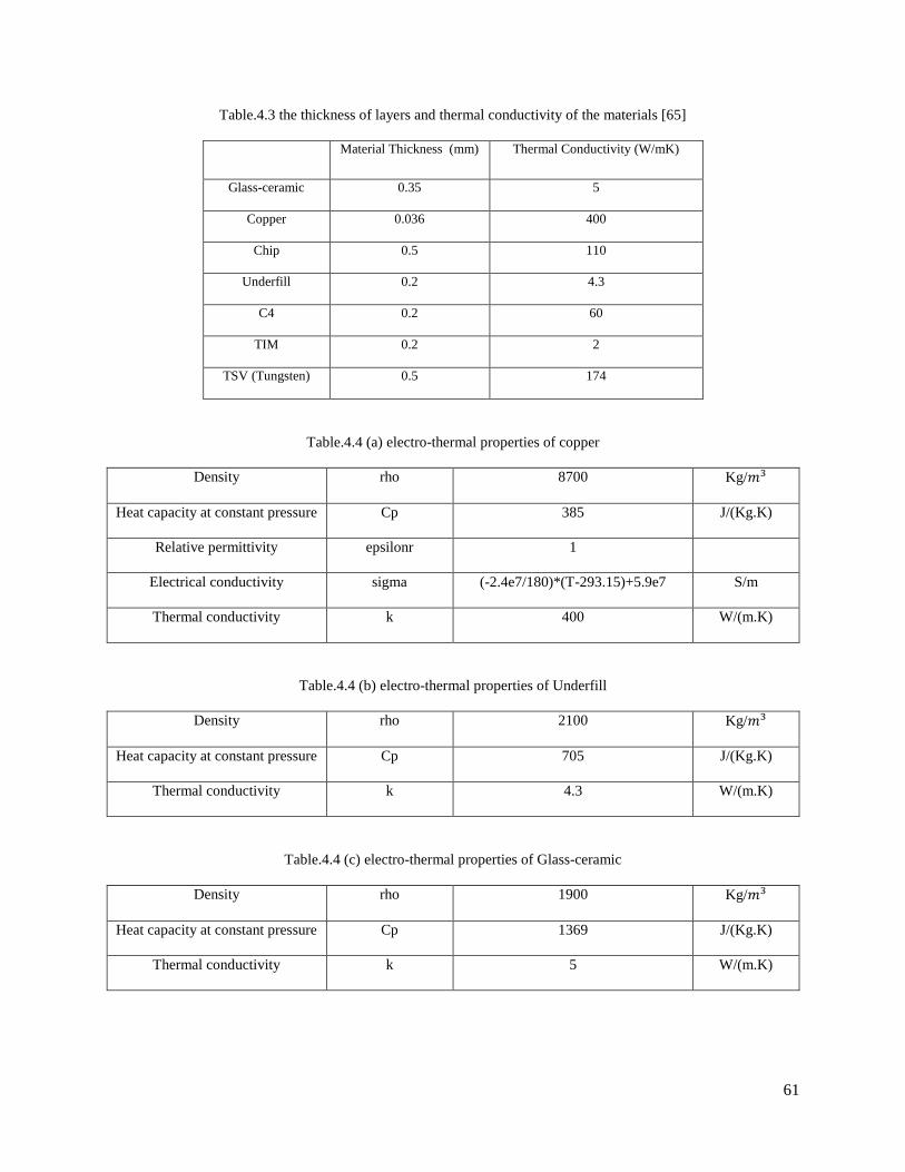
61
Table.4.3 the thickness of layers and thermal conductivity of the materials [65]
Material Thickness (mm) Thermal Conductivity (W/mK)
Glass-ceramic 0.35 5
Copper 0.036 400
Chip 0.5 110
Underfill 0.2 4.3
C4 0.2 60
TIM 0.2 2
TSV (Tungsten) 0.5 174
Table.4.4 (a) electro-thermal properties of copper
Density rho 8700 Kg/𝑚3
Heat capacity at constant pressure Cp 385 J/(Kg.K)
Relative permittivity epsilonr 1
Electrical conductivity sigma (-2.4e7/180)*(T-293.15)+5.9e7 S/m
Thermal conductivity k 400 W/(m.K)
Table.4.4 (b) electro-thermal properties of Underfill
Density rho 2100 Kg/𝑚3
Heat capacity at constant pressure Cp 705 J/(Kg.K)
Thermal conductivity k 4.3 W/(m.K)
Table.4.4 (c) electro-thermal properties of Glass-ceramic
Density rho 1900 Kg/𝑚3
Heat capacity at constant pressure Cp 1369 J/(Kg.K)
Thermal conductivity k 5 W/(m.K)
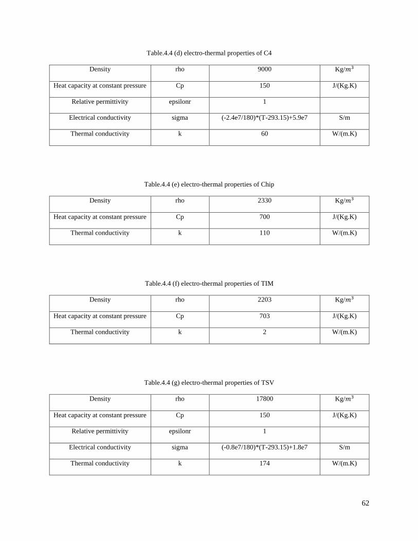
62
Table.4.4 (d) electro-thermal properties of C4
Density rho 9000 Kg/𝑚3
Heat capacity at constant pressure Cp 150 J/(Kg.K)
Relative permittivity epsilonr 1
Electrical conductivity sigma (-2.4e7/180)*(T-293.15)+5.9e7 S/m
Thermal conductivity k 60 W/(m.K)
Table.4.4 (e) electro-thermal properties of Chip
Density rho 2330 Kg/𝑚3
Heat capacity at constant pressure Cp 700 J/(Kg.K)
Thermal conductivity k 110 W/(m.K)
Table.4.4 (f) electro-thermal properties of TIM
Density rho 2203 Kg/𝑚3
Heat capacity at constant pressure Cp 703 J/(Kg.K)
Thermal conductivity k 2 W/(m.K)
Table.4.4 (g) electro-thermal properties of TSV
Density rho 17800 Kg/𝑚3
Heat capacity at constant pressure Cp 150 J/(Kg.K)
Relative permittivity epsilonr 1
Electrical conductivity sigma (-0.8e7/180)*(T-293.15)+1.8e7 S/m
Thermal conductivity k 174 W/(m.K)
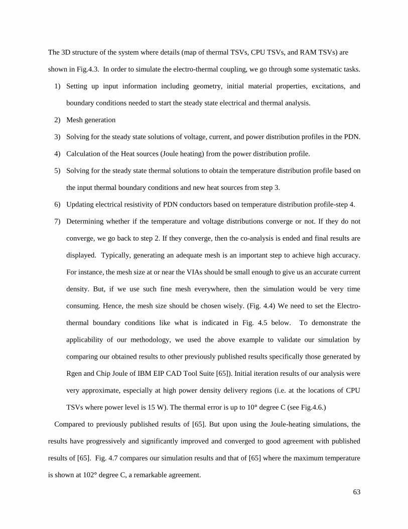
63
The 3D structure of the system where details (map of thermal TSVs, CPU TSVs, and RAM TSVs) are
shown in Fig.4.3. In order to simulate the electro-thermal coupling, we go through some systematic tasks.
1) Setting up input information including geometry, initial material properties, excitations, and
boundary conditions needed to start the steady state electrical and thermal analysis.
2) Mesh generation
3) Solving for the steady state solutions of voltage, current, and power distribution profiles in the PDN.
4) Calculation of the Heat sources (Joule heating) from the power distribution profile.
5) Solving for the steady state thermal solutions to obtain the temperature distribution profile based on
the input thermal boundary conditions and new heat sources from step 3.
6) Updating electrical resistivity of PDN conductors based on temperature distribution profile-step 4.
7) Determining whether if the temperature and voltage distributions converge or not. If they do not
converge, we go back to step 2. If they converge, then the co-analysis is ended and final results are
displayed. Typically, generating an adequate mesh is an important step to achieve high accuracy.
For instance, the mesh size at or near the VIAs should be small enough to give us an accurate current
density. But, if we use such fine mesh everywhere, then the simulation would be very time
consuming. Hence, the mesh size should be chosen wisely. (Fig. 4.4) We need to set the Electro-
thermal boundary conditions like what is indicated in Fig. 4.5 below. To demonstrate the
applicability of our methodology, we used the above example to validate our simulation by
comparing our obtained results to other previously published results specifically those generated by
Rgen and Chip Joule of IBM EIP CAD Tool Suite [65]). Initial iteration results of our analysis were
very approximate, especially at high power density delivery regions (i.e. at the locations of CPU
TSVs where power level is 15 W). The thermal error is up to 10° degree C (see Fig.4.6.)
Compared to previously published results of [65]. But upon using the Joule-heating simulations, the
results have progressively and significantly improved and converged to good agreement with published
results of [65]. Fig. 4.7 compares our simulation results and that of [65] where the maximum temperature
is shown at 102° degree C, a remarkable agreement.
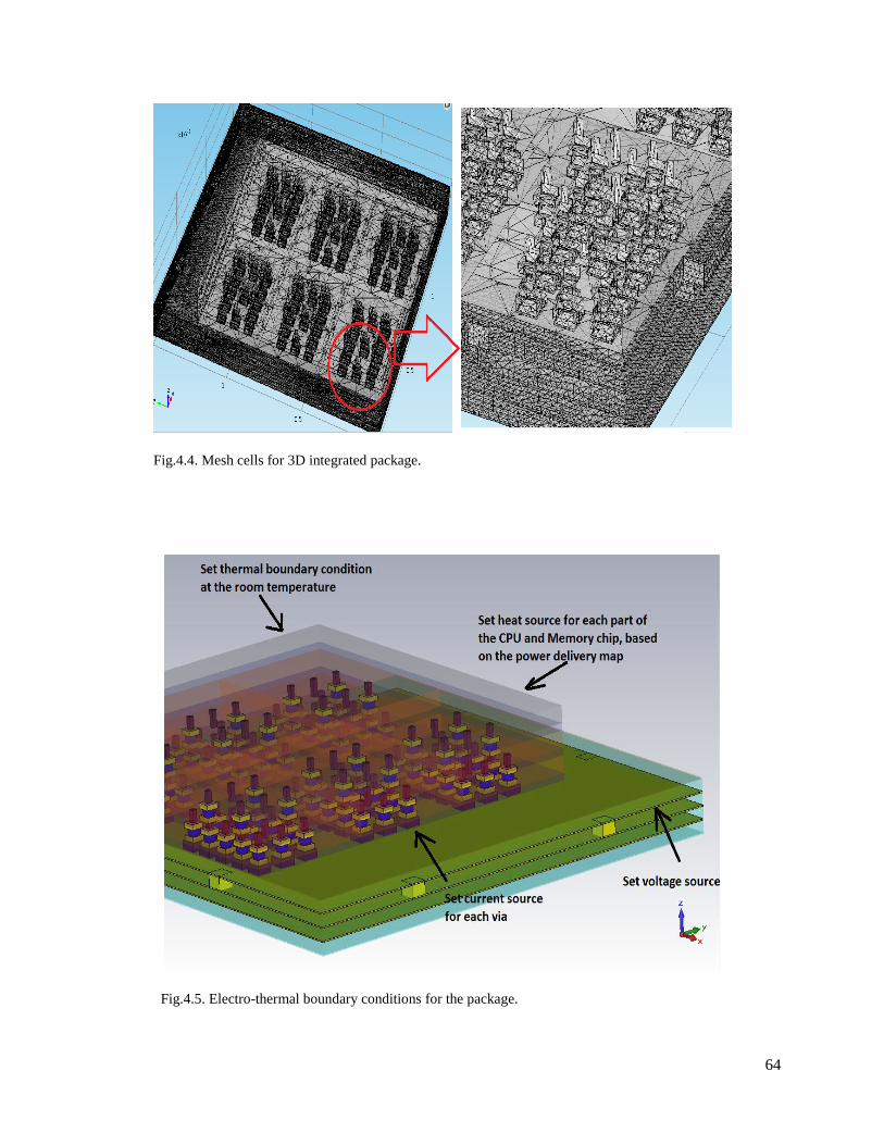
64
Fig.4.4. Mesh cells for 3D integrated package.
Fig.4.5. Electro-thermal boundary conditions for the package.
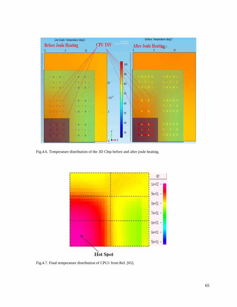
65
Fig.4.6. Temperature distribution of the 3D Chip before and after joule heating.
Fig.4.7. Final temperature distribution of CPU1 from Ref. [65].
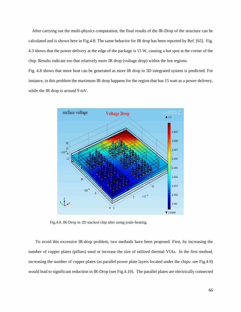
66
After carrying out the multi-physics computation, the final results of the IR-Drop of the structure can be
calculated and is shown here in Fig.4.8. The same behavior for IR drop has been reported by Ref. [65]. Fig.
4.3 shows that the power delivery at the edge of the package is 15 W, causing a hot spot at the corner of the
chip. Results indicate too that relatively more IR drop (voltage drop) within the hot regions.
Fig. 4.8 shows that more heat can be generated as more IR drop in 3D integrated system is predicted. For
instance, in this problem the maximum IR drop happens for the region that has 15 watt as a power delivery,
while the IR drop is around 9 mV.
Fig.4.8. IR-Drop in 3D stacked chip after using joule-heating.
To avoid this excessive IR-drop problem, two methods have been proposed. First, by increasing the
number of copper plates (pillars) used or increase the size of utilized thermal VIAs. In the first method,
increasing the number of copper plates (as parallel power plate layers located under the chips- see Fig.4.9)
would lead to significant reduction in IR-Drop (see Fig.4.10). The parallel plates are electrically connected
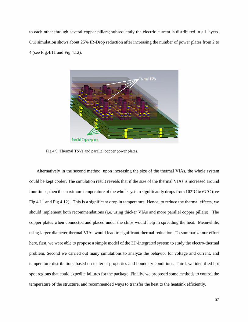
67
to each other through several copper pillars; subsequently the electric current is distributed in all layers.
Our simulation shows about 25% IR-Drop reduction after increasing the number of power plates from 2 to
4 (see Fig.4.11 and Fig.4.12).
Fig.4.9. Thermal TSVs and parallel copper power plates.
Alternatively in the second method, upon increasing the size of the thermal VIAs, the whole system
could be kept cooler. The simulation result reveals that if the size of the thermal VIAs is increased around
four times, then the maximum temperature of the whole system significantly drops from 102˚C to 67˚C (see
Fig.4.11 and Fig.4.12). This is a significant drop in temperature. Hence, to reduce the thermal effects, we
should implement both recommendations (i.e. using thicker VIAs and more parallel copper pillars). The
copper plates when connected and placed under the chips would help in spreading the heat. Meanwhile,
using larger diameter thermal VIAs would lead to significant thermal reduction. To summarize our effort
here, first, we were able to propose a simple model of the 3D-integrated system to study the electro-thermal
problem. Second we carried out many simulations to analyze the behavior for voltage and current, and
temperature distributions based on material properties and boundary conditions. Third, we identified hot
spot regions that could expedite failures for the package. Finally, we proposed some methods to control the
temperature of the structure, and recommended ways to transfer the heat to the heatsink efficiently.
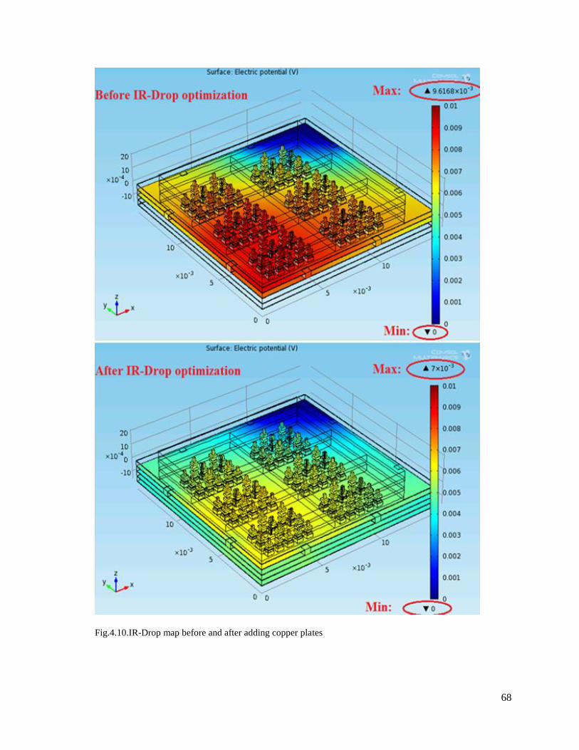
68
Fig.4.10.IR-Drop map before and after adding copper plates
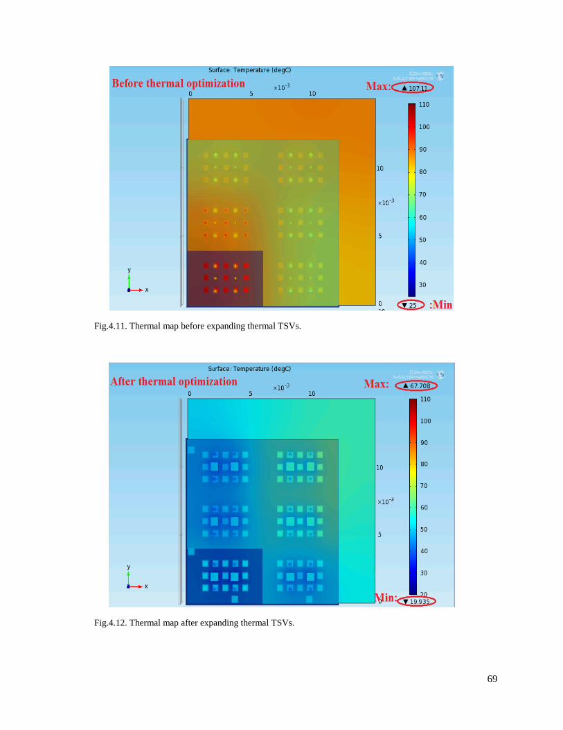
69
Fig.4.11. Thermal map before expanding thermal TSVs.
Fig.4.12. Thermal map after expanding thermal TSVs.

70
4.3.2. Modeling of 3D electro-thermal -3D daisy chain
Daisy Chain test die are used in life cycle testing, drop testing, measurements of CTE (Coefficient of
Thermal Expansion), selection of the correct amount of solder paste, evaluation of solder paste stencils,
check for voids caused during reflow and under fill experiments, etc. [66]. The use of the daisy chains
helps in optimizing the assembly process. Daisy Chain is made by stitching gold bonding wire between
pairs of bonding pads on the lead frame. BGA and CSP Daisy Chain are usually made with copper traces
between pairs of ball pads on the substrate. Here, we model a daisy chain embossed inside an electronic
3D integrated circuit (see Fig.4.13). Ref [66] is used to validate our 3D multi-physics model. In this
example, we simulate a daisy chain embossed inside a silicon chip as seen in Fig. 4.14. One of the main
concerns when using daisy chain interconnects is that while the electrical current flows though the daisy
chain, the electric current distribution drastically increases when getting in or out of the VIAs, i.e. the
point between the pad trace and the solder pillar (see Fig. 4.15). This phenomenon is called current
crowding and can cause a serious problem due to the possibility of a thermo-electro-migration failure.
The main reason of this failure is that the temperature rises up very quickly, and it can create serious
damages for the atomic structure of the material used as a bump. Additionally, electro-migration
accelerates this process as well. As a result, the physical structure can’t tolerate this high stress and
pressure. Then, it causes deformation, and eventually a failure (see Fig. 4.16). Table 4.5 shows a very
good agreement between our simulation result and the data (measured and calculated as extracted from
Ref. [66]). As a remedy for such failure, we utilized a simple method that was recommended by [68].
The method is based on finding a way to distribute the electric current through several paths instead of
one. Where all utilized paths should be connected to the solder pillar from different directions, so it will
prevent the flow of electric current in only one tiny region and provide adequate spreading (see Fig. 4.17).
The excellent agreement demonstrates that our 3D multi-physics model can predict the heat spreading in
interconnects and the reduction of the thermal problem.
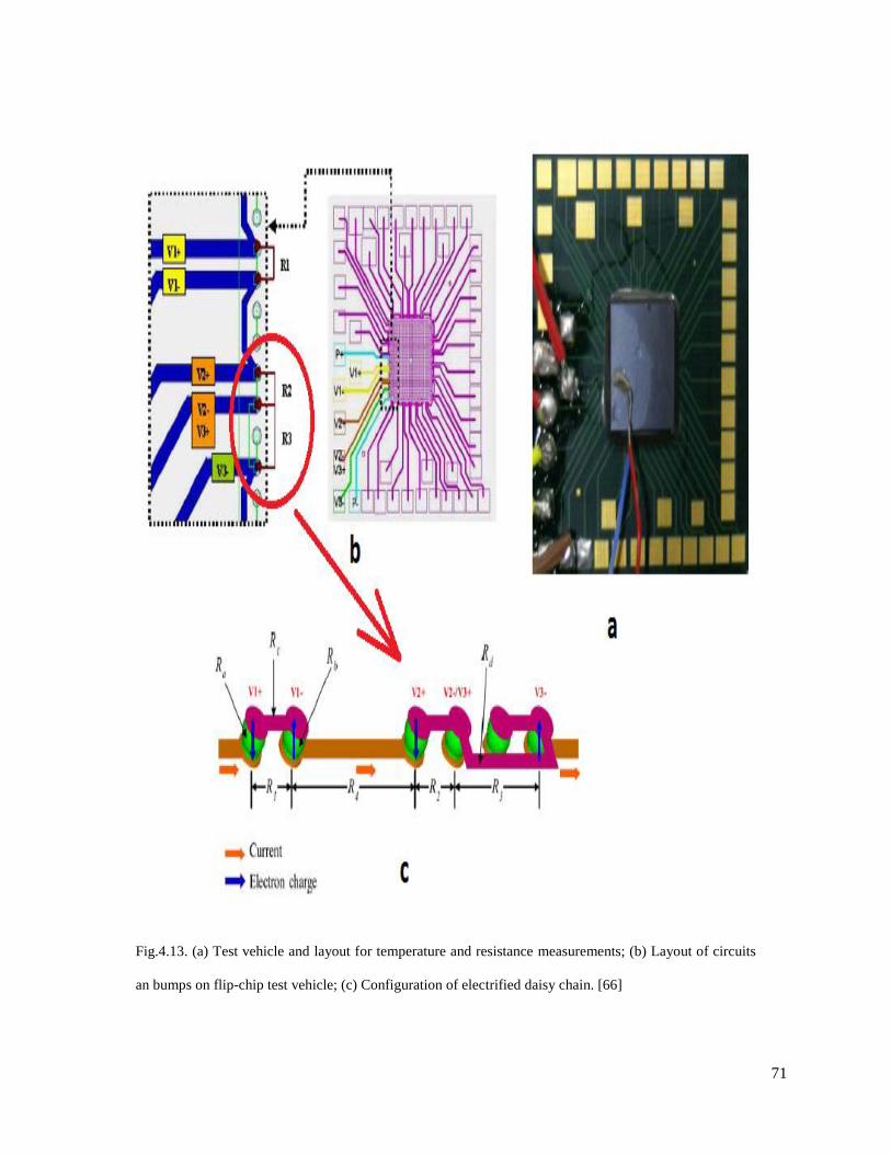
71
Fig.4.13. (a) Test vehicle and layout for temperature and resistance measurements; (b) Layout of circuits
an bumps on flip-chip test vehicle; (c) Configuration of electrified daisy chain. [66]
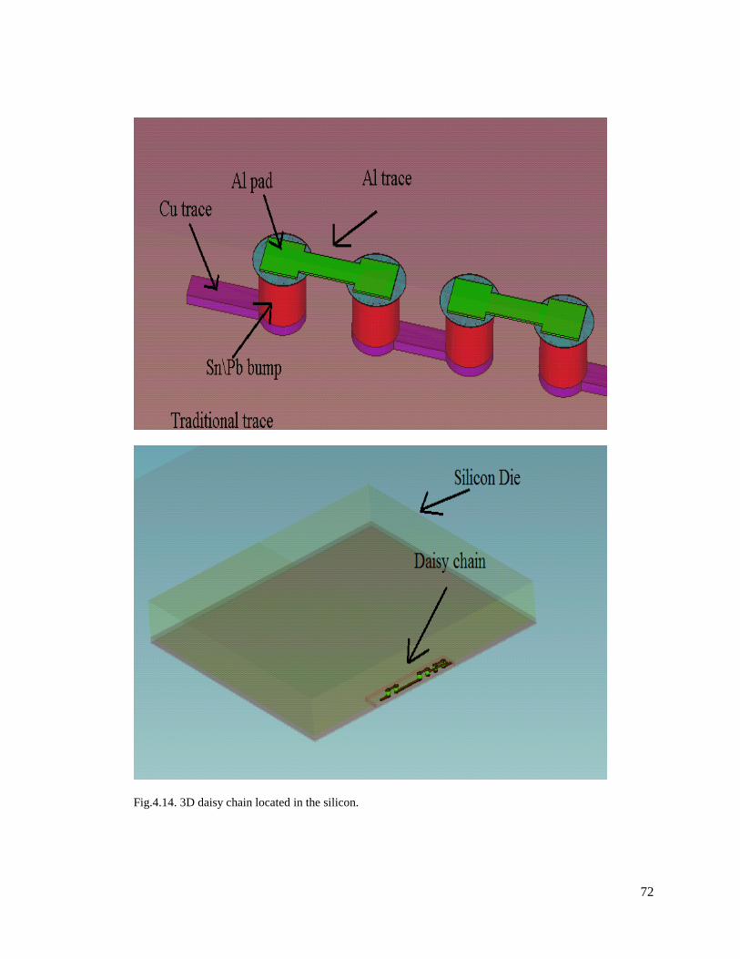
72
Fig.4.14. 3D daisy chain located in the silicon.
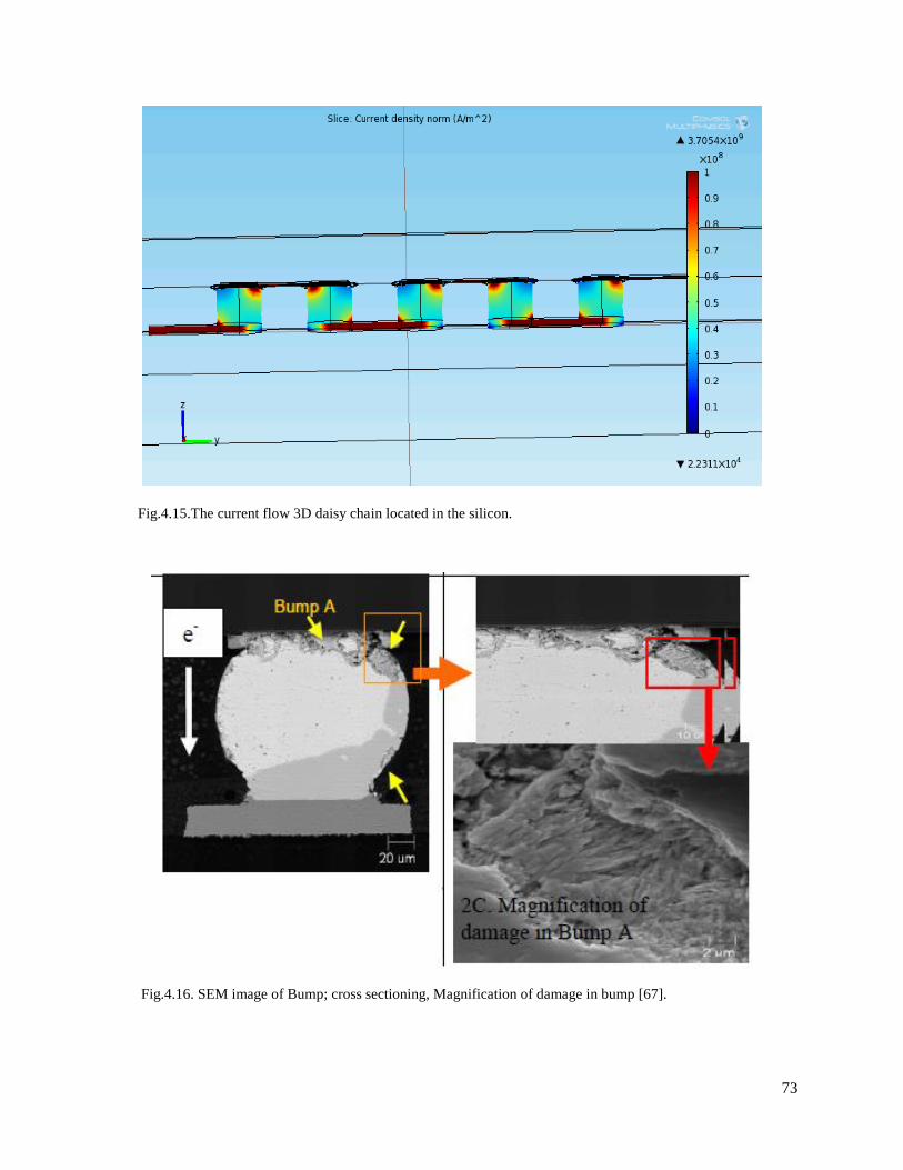
73
Fig.4.15.The current flow 3D daisy chain located in the silicon.
Fig.4.16. SEM image of Bump; cross sectioning, Magnification of damage in bump [67].
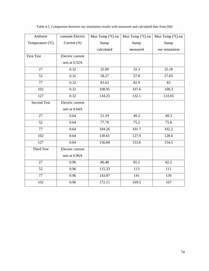
74
Table.4.5. Comparison between our simulation results with measured and calculated data from [66]
Ambient
Temperature (℃)
constant Electric
Current (A)
Max Temp (℃) on
bump
calculated
Max Temp (℃) on
bump
measured
Max Temp (℃) on
bump
our simulation
First Test
Electric current
sets at 0.32A
27 0.32 32.89 32.3 32.28
52 0.32 58.27 57.8 57.65
77 0.32 83.63 82.9 83
102 0.32 108.95 107.6 108.3
127 0.32 134.25 132.1 133.65
Second Test
Electric current
sets at 0.64A
27 0.64 51.19 49.2 49.3
52 0.64 77.79 75.2 75.8
77 0.64 104.26 101.7 102.2
102 0.64 130.61 127.9 128.6
127 0.64 156.84 153.6 154.5
Third Test
Electric current
sets at 0.96A
27 0.96 86.48 85.5 82.5
52 0.96 115.33 113 111
77 0.96 143.87 141 139
102 0.96 172.11 169.5 167
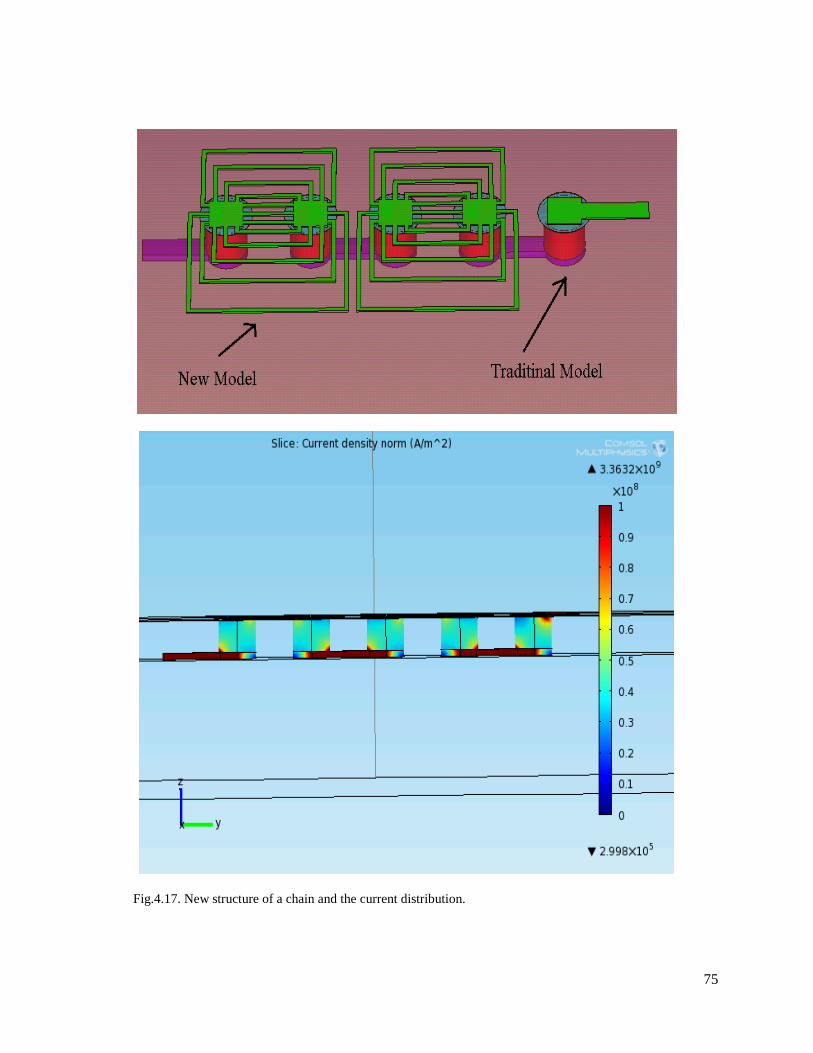
75
Fig.4.17. New structure of a chain and the current distribution.

76
4.4. Analysis of 3D electro-thermal simulation for devices at high frequencies
4.4.1. Analysis of 3D electro-thermal simulations- GaN device power amplifier
With the fast progress in GaN technology, the level of high power density has seen a large surge in the
last few years. However, reliability is still an issue and the first step to improve its reliability is to control
the temperature at the transistors’ junctions for the power amplifier-GaN device-- so it does not exceed
125° Deg C.
Various methods have been recommended to provide efficient heat sinking, here we will use a thick
copper plate (as a heat sink), and a thin film Thermal Interface Material (TIM) between the heatsink and
the GaN device to provide efficient heat spreading.
In our study, we will use our electro-thermal model to design an optimized heat sink for high power space
combining scheme. The space combiner is composed of a stack of amplifiers in a very small volume
(stacked-trays).
Each tray is comprised of three stages of amplification; the first is a driver amplifier that feeds two
medium power amplifier stages through a 1:2 splitter. The output of each medium power amplifier is split
again into two routes and each is driving a high power amplifier, i.e. each tray has total of 7 amplifiers.
These four final stages MMIC power amplifier devices are located side by side each other, and they are
combined together through a 4 to 1 power combiner.
Four stacked trays are mounted on top of each other (as seen in Fig. 4.18), and finally all outputs are
combined together to one output power using space combining techniques.
Again, we are interested in investigating the thermal problem in this multi-stack amplifier and design an
efficient heat sink. Fig 4.19 shows one amplifier that is divided into different layers, like dc PCB board, RF
board, TIM, GaN device.
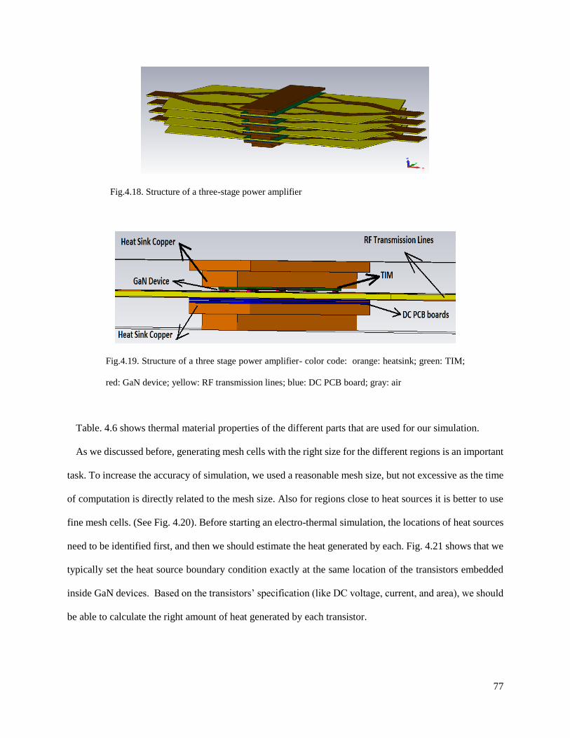
77
Fig.4.18. Structure of a three-stage power amplifier
Fig.4.19. Structure of a three stage power amplifier- color code: orange: heatsink; green: TIM;
red: GaN device; yellow: RF transmission lines; blue: DC PCB board; gray: air
Table. 4.6 shows thermal material properties of the different parts that are used for our simulation.
As we discussed before, generating mesh cells with the right size for the different regions is an important
task. To increase the accuracy of simulation, we used a reasonable mesh size, but not excessive as the time
of computation is directly related to the mesh size. Also for regions close to heat sources it is better to use
fine mesh cells. (See Fig. 4.20). Before starting an electro-thermal simulation, the locations of heat sources
need to be identified first, and then we should estimate the heat generated by each. Fig. 4.21 shows that we
typically set the heat source boundary condition exactly at the same location of the transistors embedded
inside GaN devices. Based on the transistors’ specification (like DC voltage, current, and area), we should
be able to calculate the right amount of heat generated by each transistor.
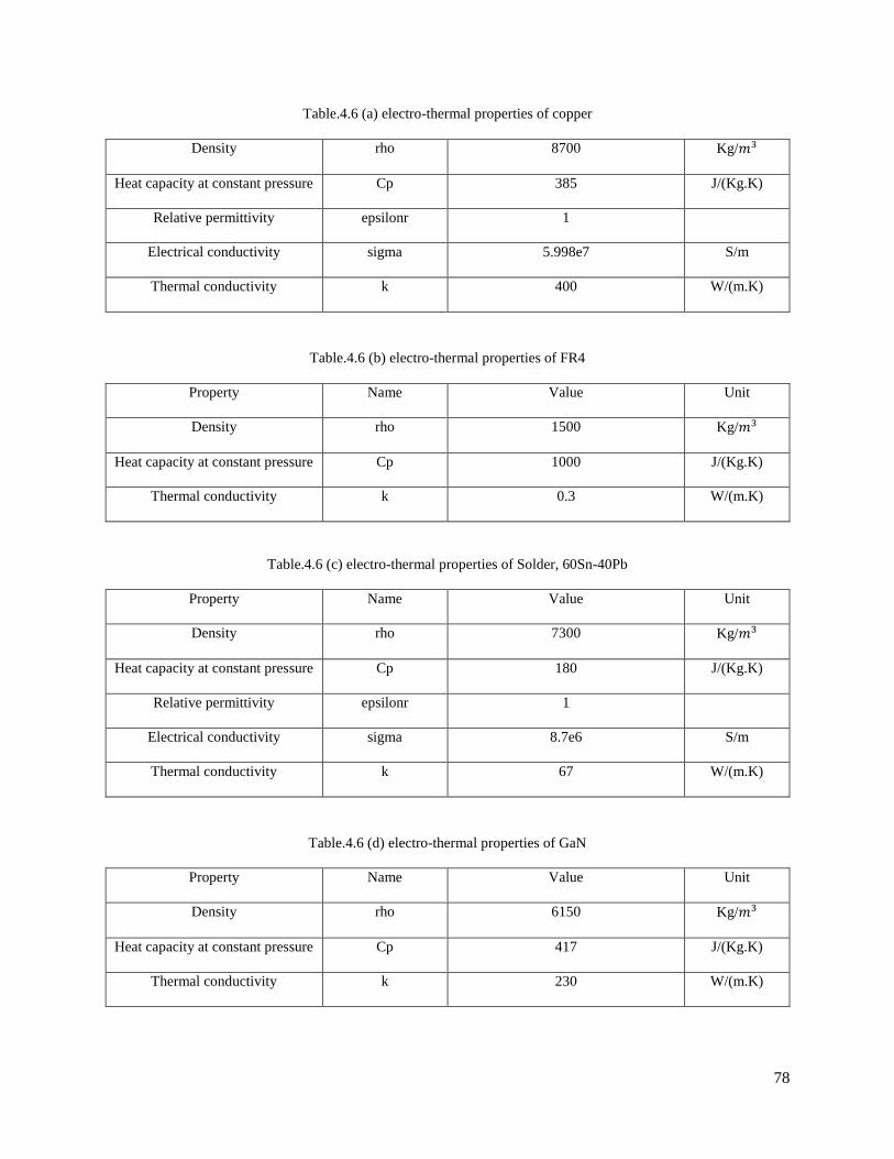
78
Table.4.6 (a) electro-thermal properties of copper
Density rho 8700 Kg/𝑚3
Heat capacity at constant pressure Cp 385 J/(Kg.K)
Relative permittivity epsilonr 1
Electrical conductivity sigma 5.998e7 S/m
Thermal conductivity k 400 W/(m.K)
Table.4.6 (b) electro-thermal properties of FR4
Property Name Value Unit
Density rho 1500 Kg/𝑚3
Heat capacity at constant pressure Cp 1000 J/(Kg.K)
Thermal conductivity k 0.3 W/(m.K)
Table.4.6 (c) electro-thermal properties of Solder, 60Sn-40Pb
Property Name Value Unit
Density rho 7300 Kg/𝑚3
Heat capacity at constant pressure Cp 180 J/(Kg.K)
Relative permittivity epsilonr 1
Electrical conductivity sigma 8.7e6 S/m
Thermal conductivity k 67 W/(m.K)
Table.4.6 (d) electro-thermal properties of GaN
Property Name Value Unit
Density rho 6150 Kg/𝑚3
Heat capacity at constant pressure Cp 417 J/(Kg.K)
Thermal conductivity k 230 W/(m.K)
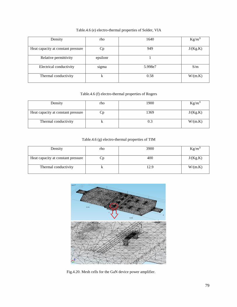
79
Table.4.6 (e) electro-thermal properties of Solder, VIA
Density rho 1640 Kg/𝑚3
Heat capacity at constant pressure Cp 949 J/(Kg.K)
Relative permittivity epsilonr 1
Electrical conductivity sigma 5.998e7 S/m
Thermal conductivity k 0.58 W/(m.K)
Table.4.6 (f) electro-thermal properties of Rogers
Density rho 1900 Kg/𝑚3
Heat capacity at constant pressure Cp 1369 J/(Kg.K)
Thermal conductivity k 0.3 W/(m.K)
Table.4.6 (g) electro-thermal properties of TIM
Density rho 3900 Kg/𝑚3
Heat capacity at constant pressure Cp 400 J/(Kg.K)
Thermal conductivity k 12.9 W/(m.K)
Fig.4.20. Mesh cells for the GaN device power amplifier.
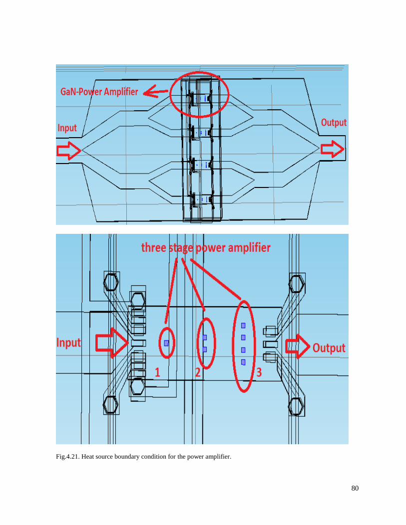
80
Fig.4.21. Heat source boundary condition for the power amplifier.
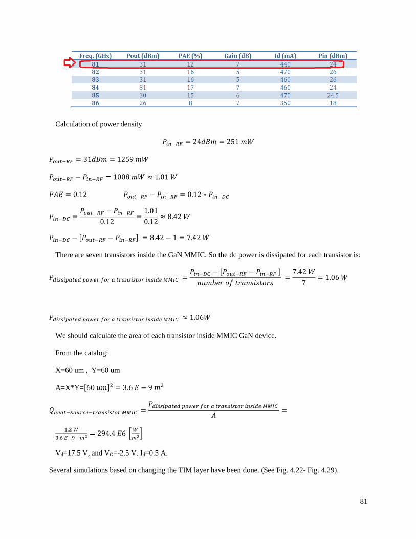
81
Calculation of power density
𝑃𝑖𝑛−𝑅𝐹 = 24𝑑𝐵𝑚 = 251 𝑚𝑊
𝑃𝑜𝑢𝑡−𝑅𝐹 = 31𝑑𝐵𝑚 = 1259 𝑚𝑊
𝑃𝑜𝑢𝑡−𝑅𝐹 − 𝑃𝑖𝑛−𝑅𝐹 = 1008 𝑚𝑊 ≈ 1.01 𝑊
𝑃𝐴𝐸 = 0.12 𝑃𝑜𝑢𝑡−𝑅𝐹 − 𝑃𝑖𝑛−𝑅𝐹 = 0.12 ∗ 𝑃𝑖𝑛−𝐷𝐶
𝑃𝑖𝑛−𝐷𝐶 =𝑃𝑜𝑢𝑡−𝑅𝐹 − 𝑃𝑖𝑛−𝑅𝐹
0.12=
1.01
0.12≈ 8.42 𝑊
𝑃𝑖𝑛−𝐷𝐶 − [𝑃𝑜𝑢𝑡−𝑅𝐹 − 𝑃𝑖𝑛−𝑅𝐹] = 8.42 − 1 = 7.42 𝑊
There are seven transistors inside the GaN MMIC. So the dc power is dissipated for each transistor is:
𝑃𝑑𝑖𝑠𝑠𝑖𝑝𝑎𝑡𝑒𝑑 𝑝𝑜𝑤𝑒𝑟 𝑓𝑜𝑟 𝑎 𝑡𝑟𝑎𝑛𝑠𝑖𝑠𝑡𝑜𝑟 𝑖𝑛𝑠𝑖𝑑𝑒 𝑀𝑀𝐼𝐶 =𝑃𝑖𝑛−𝐷𝐶 − [𝑃𝑜𝑢𝑡−𝑅𝐹 − 𝑃𝑖𝑛−𝑅𝐹 ]
𝑛𝑢𝑚𝑏𝑒𝑟 𝑜𝑓 𝑡𝑟𝑎𝑛𝑠𝑖𝑠𝑡𝑜𝑟𝑠 =
7.42 𝑊
7= 1.06 𝑊
𝑃𝑑𝑖𝑠𝑠𝑖𝑝𝑎𝑡𝑒𝑑 𝑝𝑜𝑤𝑒𝑟 𝑓𝑜𝑟 𝑎 𝑡𝑟𝑎𝑛𝑠𝑖𝑠𝑡𝑜𝑟 𝑖𝑛𝑠𝑖𝑑𝑒 𝑀𝑀𝐼𝐶 ≈ 1.06𝑊
We should calculate the area of each transistor inside MMIC GaN device.
From the catalog:
X=60 um , Y=60 um
A=X*Y=[60 𝑢𝑚]2 = 3.6 𝐸 − 9 𝑚2
𝑄ℎ𝑒𝑎𝑡−𝑆𝑜𝑢𝑟𝑐𝑒−𝑡𝑟𝑎𝑛𝑠𝑖𝑠𝑡𝑜𝑟 𝑀𝑀𝐼𝐶 =𝑃𝑑𝑖𝑠𝑠𝑖𝑝𝑎𝑡𝑒𝑑 𝑝𝑜𝑤𝑒𝑟 𝑓𝑜𝑟 𝑎 𝑡𝑟𝑎𝑛𝑠𝑖𝑠𝑡𝑜𝑟 𝑖𝑛𝑠𝑖𝑑𝑒 𝑀𝑀𝐼𝐶
𝐴=
1.2 𝑊
3.6 𝐸−9 𝑚2 = 294.4 𝐸6 [𝑊
𝑚2]
Vd=17.5 V, and VG=-2.5 V. Id=0.5 A.
Several simulations based on changing the TIM layer have been done. (See Fig. 4.22- Fig. 4.29).

82
Fig.4.22. Thermal distribution on the surface and inside the RF power amplifier when the thickness of
TIM layer is 1 mil and the thermal conductivity is 12.9[W/(m*K)].
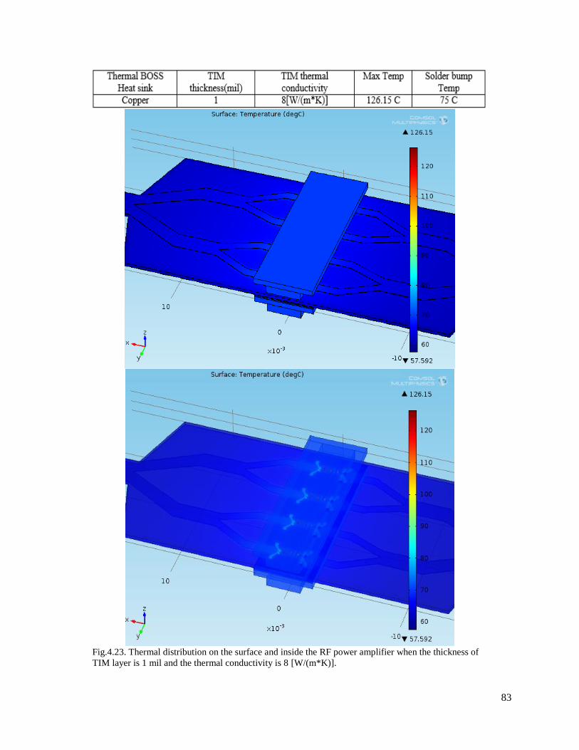
83
Fig.4.23. Thermal distribution on the surface and inside the RF power amplifier when the thickness of
TIM layer is 1 mil and the thermal conductivity is 8 [W/(m*K)].
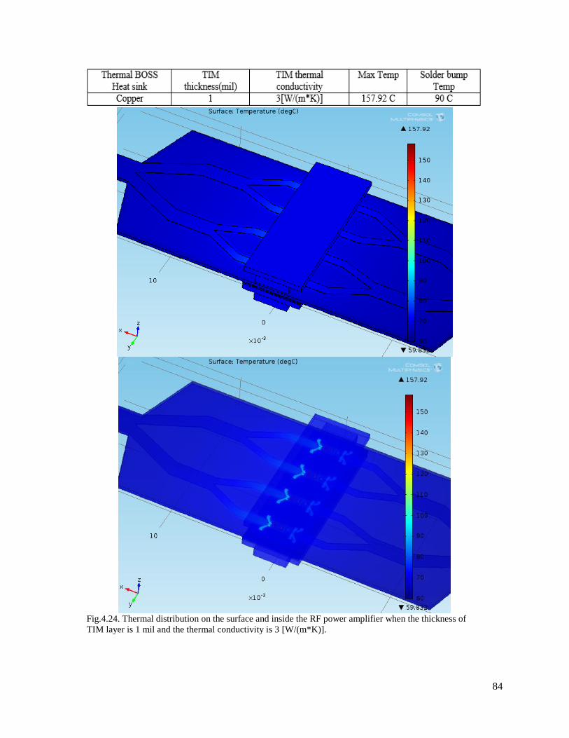
84
Fig.4.24. Thermal distribution on the surface and inside the RF power amplifier when the thickness of
TIM layer is 1 mil and the thermal conductivity is 3 [W/(m*K)].
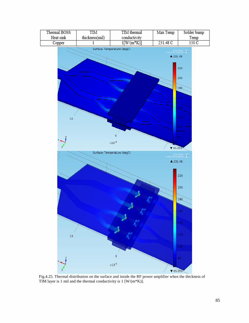
85
Fig.4.25. Thermal distribution on the surface and inside the RF power amplifier when the thickness of
TIM layer is 1 mil and the thermal conductivity is 1 [W/(m*K)].

86
Fig.4.26. Thermal distribution on the surface and inside the RF power amplifier when the thickness of
TIM layer is 3 mil and the thermal conductivity is 12.9 [W/(m*K)].

87
Fig.4.27. Thermal distribution on the surface and inside the RF power amplifier when the thickness of
TIM layer is 1 mil and the thermal conductivity is 12.9 [W/(m*K)].
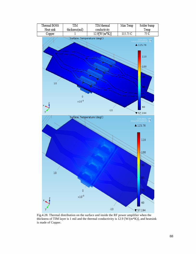
88
Fig.4.28. Thermal distribution on the surface and inside the RF power amplifier when the
thickness of TIM layer is 1 mil and the thermal conductivity is 12.9 [W/(m*K)], and heatsink
is made of Copper.
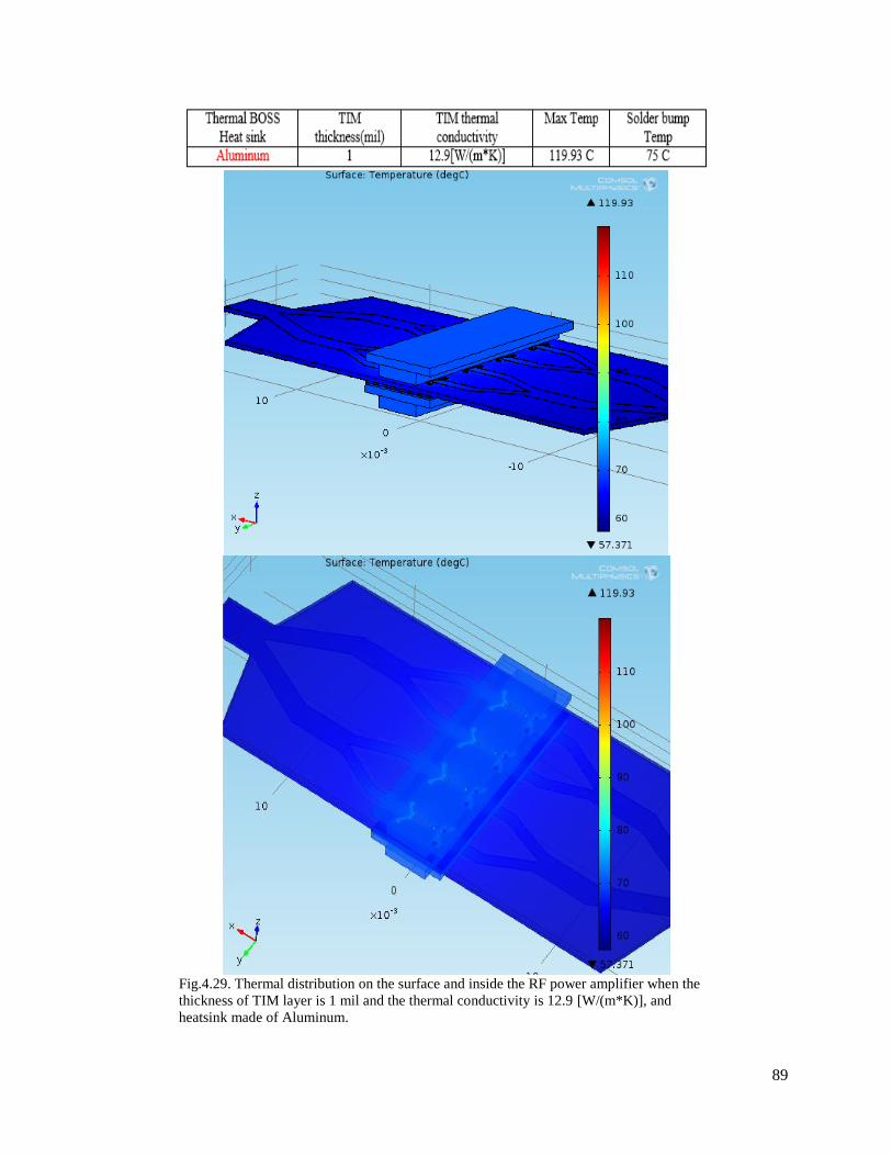
89
Fig.4.29. Thermal distribution on the surface and inside the RF power amplifier when the
thickness of TIM layer is 1 mil and the thermal conductivity is 12.9 [W/(m*K)], and
heatsink made of Aluminum.
90
4.5. Conclusion
Our developed multi-physics models and proposed solver scheme are developed to resolve the electro-
thermal problems for different electronic systems, and definitely could clearly describe how the electric
current flowing through the conductors can cause a voltage drop creating hot spots. The developed joule
heating 3D multi-physics module is based on utilizing partial differential equations PDEs that are solved in
COMSOL. To validate our models, however, we picked various structures that were previously measured
and published and compared our simulated results with their measurements and excellent agreement were
achieved.
In the first example, a 3D stacked chip was used to demonstrate that increasing the number of copper
parallel layers or the size of thermal Through Silicon VIAs TSVs could keep the electronic circuits
relatively cool. In the second example we investigated failure mechanisms in daisy chains, to be specific,
we discussed the controversial failure problem, which happens for solder pillar/copper bump in the silicon
chip. The results of the simulation showed that the current crowding phenomenon or thermal-electro-
migration could cause such failure.
A remedy to prevent this problem was presented based on distributing the electric current through several
paths at the position of solder pillar/ copper bump. As a result, the electrical current does not flow in only
one tiny region. In the third example, we showed how the temperature of a transistor’s junctions could be
controlled by optimizing the utilized TIM layer (type and thickness) and heat sink material.
Finally, we conclude with the following recipe when Joule heating effect due to the current flowing
through conductors is considered.
1) Create s database for electrical resistivity or conductivity as a function of temperature.
2) The temperature effect on IR drop cannot be neglected. For instance avoiding thermal effect can
cause up to 20% error for IR drop.
3) The current crowding at hot regions need to be detected. It can be resolved by changing the size of
interconnectors or path lines for dc current.

91
4) To transfer the heat to the heatsink efficiently, a good material with right structure (size) need to
be designed.
5) It is always helpful to provide more than one path for the current either by providing // plates
connected by VIAs, or multitude of routes connected in a current junction (node). Such current splitting
can significantly reduce the power loss upon reducing the current value in each conductor, while keeping
the overall current of interconnections the same.
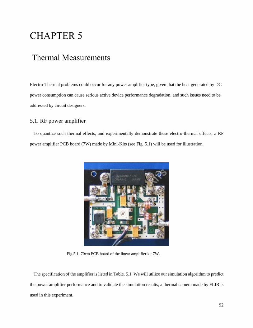
92
CHAPTER 5
Thermal Measurements
Electro-Thermal problems could occur for any power amplifier type, given that the heat generated by DC
power consumption can cause serious active device performance degradation, and such issues need to be
addressed by circuit designers.
5.1. RF power amplifier
To quantize such thermal effects, and experimentally demonstrate these electro-thermal effects, a RF
power amplifier PCB board (7W) made by Mini-Kits (see Fig. 5.1) will be used for illustration.
Fig.5.1. 70cm PCB board of the linear amplifier kit 7W.
The specification of the amplifier is listed in Table. 5.1. We will utilize our simulation algorithm to predict
the power amplifier performance and to validate the simulation results, a thermal camera made by FLIR is
used in this experiment.
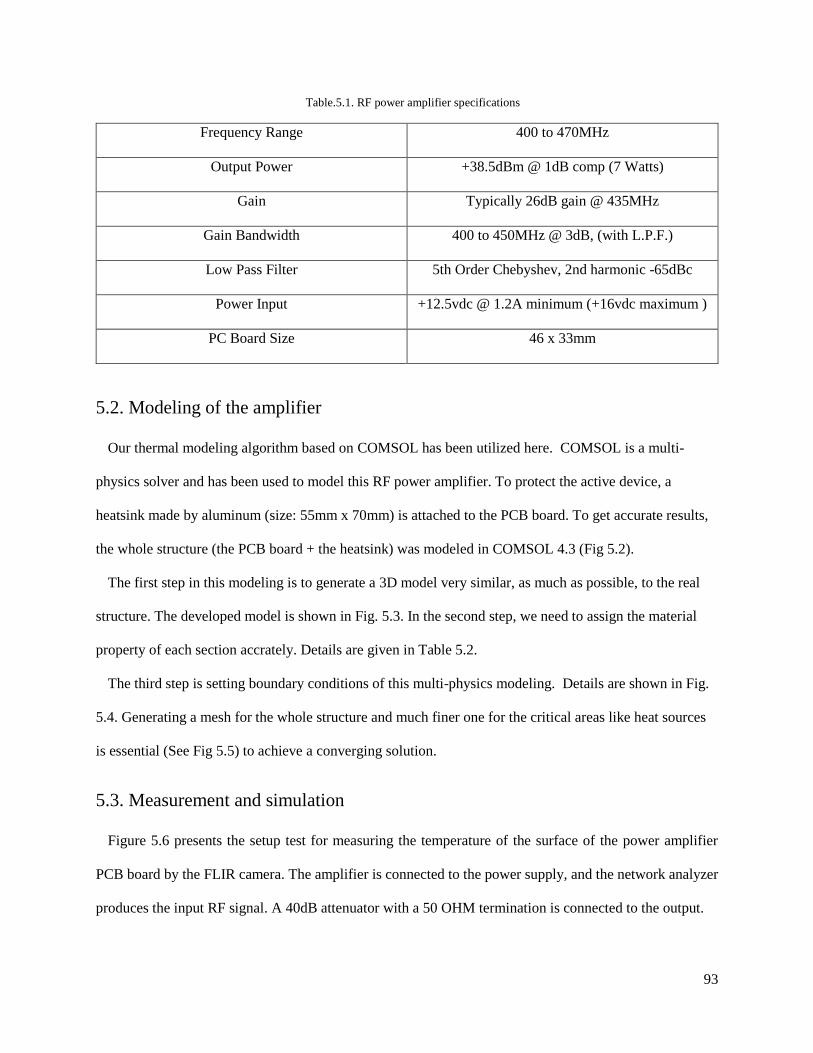
93
Table.5.1. RF power amplifier specifications
Frequency Range 400 to 470MHz
Output Power +38.5dBm @ 1dB comp (7 Watts)
Gain Typically 26dB gain @ 435MHz
Gain Bandwidth 400 to 450MHz @ 3dB, (with L.P.F.)
Low Pass Filter 5th Order Chebyshev, 2nd harmonic -65dBc
Power Input +12.5vdc @ 1.2A minimum (+16vdc maximum )
PC Board Size 46 x 33mm
5.2. Modeling of the amplifier
Our thermal modeling algorithm based on COMSOL has been utilized here. COMSOL is a multi-
physics solver and has been used to model this RF power amplifier. To protect the active device, a
heatsink made by aluminum (size: 55mm x 70mm) is attached to the PCB board. To get accurate results,
the whole structure (the PCB board + the heatsink) was modeled in COMSOL 4.3 (Fig 5.2).
The first step in this modeling is to generate a 3D model very similar, as much as possible, to the real
structure. The developed model is shown in Fig. 5.3. In the second step, we need to assign the material
property of each section accrately. Details are given in Table 5.2.
The third step is setting boundary conditions of this multi-physics modeling. Details are shown in Fig.
5.4. Generating a mesh for the whole structure and much finer one for the critical areas like heat sources
is essential (See Fig 5.5) to achieve a converging solution.
5.3. Measurement and simulation
Figure 5.6 presents the setup test for measuring the temperature of the surface of the power amplifier
PCB board by the FLIR camera. The amplifier is connected to the power supply, and the network analyzer
produces the input RF signal. A 40dB attenuator with a 50 OHM termination is connected to the output.
94
Fig.5.2. Prototyped version and the generated model in COMSOL
Fig.5.3. 3D model of the structure built in COMSOL
Table.5.2 (a) electro-thermal properties of Aluminum
Property Name Value Unit
Density rho 2700 Kg/𝑚3
Heat capacity at constant pressure Cp 900 J/(Kg.K)
Thermal conductivity k 160 W/(m.K)
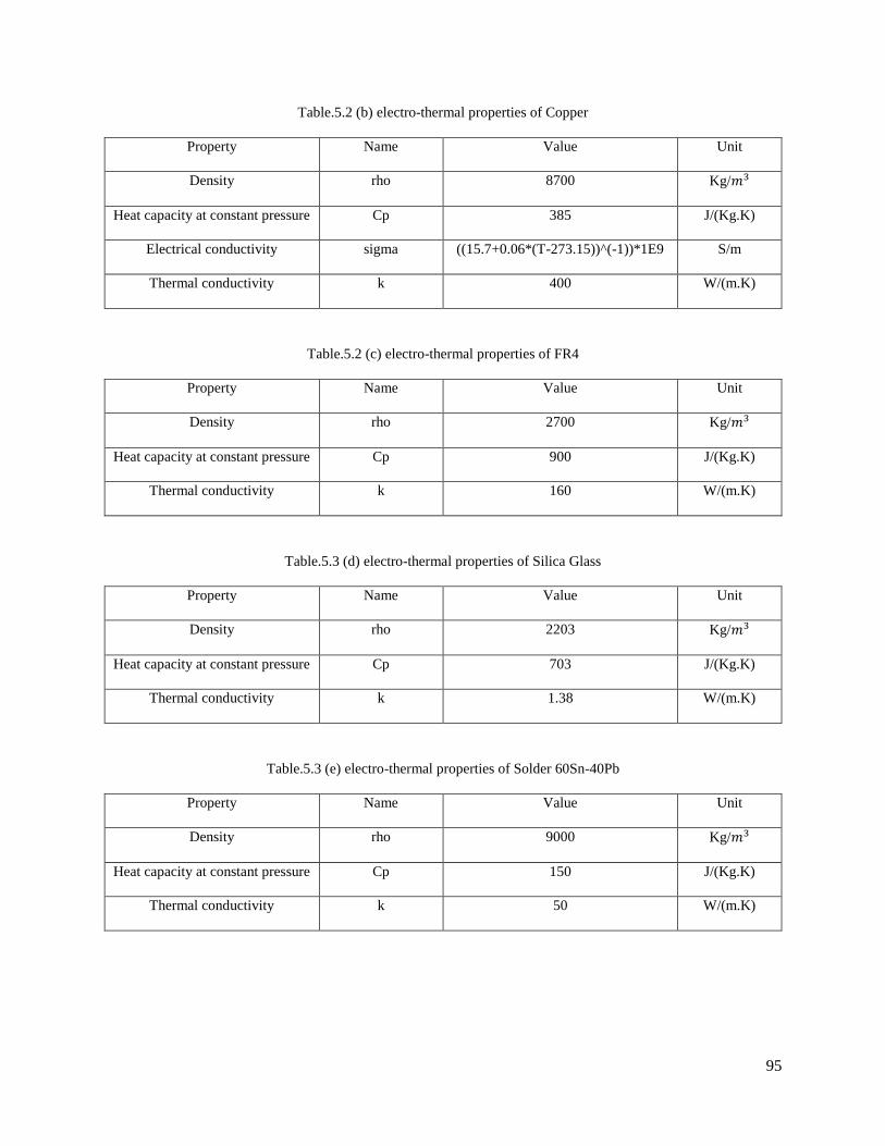
95
Table.5.2 (b) electro-thermal properties of Copper
Property Name Value Unit
Density rho 8700 Kg/𝑚3
Heat capacity at constant pressure Cp 385 J/(Kg.K)
Electrical conductivity sigma ((15.7+0.06*(T-273.15))^(-1))*1E9 S/m
Thermal conductivity k 400 W/(m.K)
Table.5.2 (c) electro-thermal properties of FR4
Property Name Value Unit
Density rho 2700 Kg/𝑚3
Heat capacity at constant pressure Cp 900 J/(Kg.K)
Thermal conductivity k 160 W/(m.K)
Table.5.3 (d) electro-thermal properties of Silica Glass
Property Name Value Unit
Density rho 2203 Kg/𝑚3
Heat capacity at constant pressure Cp 703 J/(Kg.K)
Thermal conductivity k 1.38 W/(m.K)
Table.5.3 (e) electro-thermal properties of Solder 60Sn-40Pb
Property Name Value Unit
Density rho 9000 Kg/𝑚3
Heat capacity at constant pressure Cp 150 J/(Kg.K)
Thermal conductivity k 50 W/(m.K)

96
Fig.5.4. Electric and thermal boundary conditions
Fig.5.5. Mesh Generation of the whole structure in COMSOL.

97
Figure 5.7 presents the simulation result when the fan is off. For this simulation the room temperature
was set at 23 Celsius. Since inside the MMIC device is unknown then, as a good approximation, we consider
the whole area of the device as a heat source. Fig 5.8 shows the thermal image that was captured by the
FLIR camera of the amplifier (the fan is off). A good agreement can be seen for the thermal distribution on
the surface of the MMIC device (heat source) and PCB board (FR4). However, the accuracy of the thermal
image for shiny surfaces like metallic parts isn’t good, because it can reflect light in IR region strongly to
the camera. In the second trial, we checked the effect of a fan that was located on top of the heat sink. To
consider the effect of the fan (see Fig. 5.9), we needed to add the convection cooling as a new boundary
condition. For this reason, the speed of air is calculated from the fan speed. We have carried out several
simulations based on different speeds of the air around the heat sink. Fig. 5.10 shows the simulation result
when the fan is on; for an air speed of 0.5 m/s. Fig. 5.11 shows the simulation results when the fan is on;
for air speed= 5 m/s. After comparing the measured and simulated data (see Fig 5.12), you can see a good
agreement for the heat distribution on the surface of power amplifier device, and the hot region close to the
device. For the shiny regions, the camera doesn’t show accurate results because of capturing IR noise from
the environment (resulting from strong reflections from the metallic parts). . Speed of air (m/s) =
2*π*(R1(cm))/100)*RPM/60, Fan speed: 1500 – 3500 (rpm), Speed of air: 3m/s-7m/s, Average speed:5 m/s
Fig.5.6. The setup for measuring the thermal distribution on the surface of the amplifier by FLIR camera.
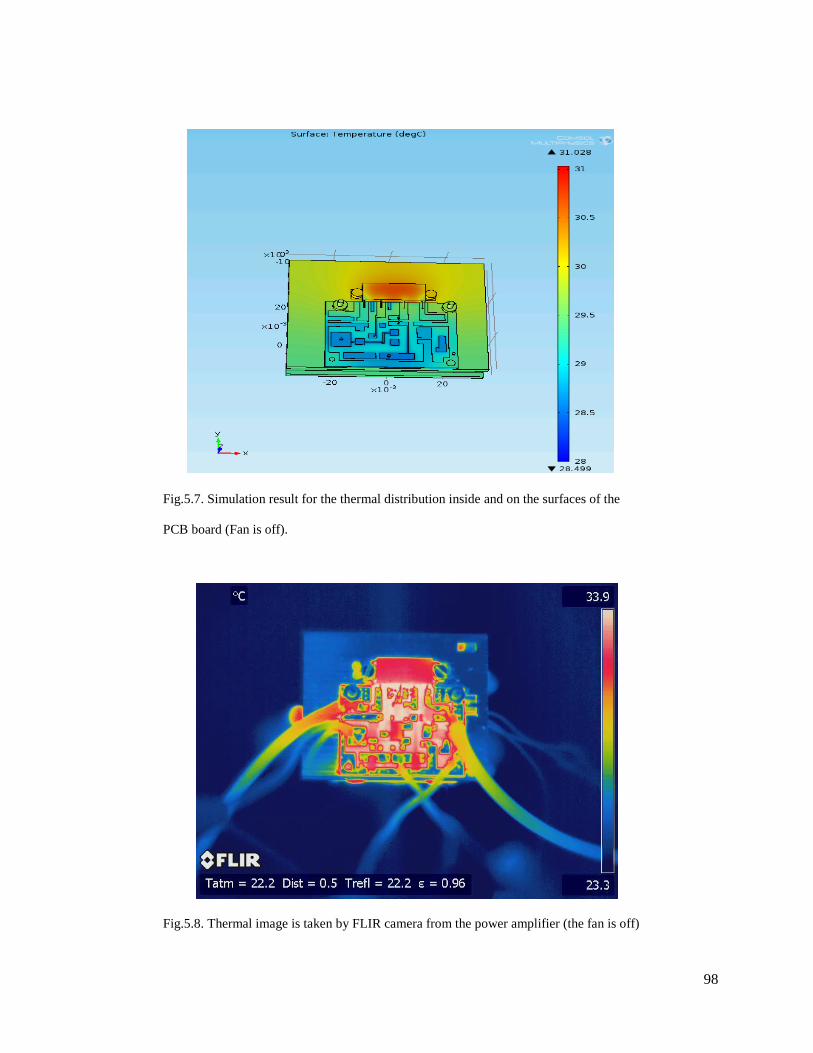
98
Fig.5.7. Simulation result for the thermal distribution inside and on the surfaces of the
PCB board (Fan is off).
Fig.5.8. Thermal image is taken by FLIR camera from the power amplifier (the fan is off)
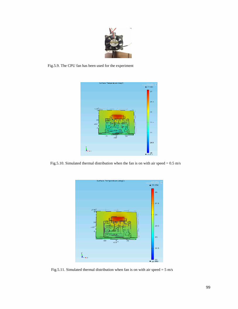
99
Fig.5.9. The CPU fan has been used for the experiment
Fig.5.10. Simulated thermal distribution when the fan is on with air speed = 0.5 m/s
Fig.5.11. Simulated thermal distribution when fan is on with air speed = 5 m/s
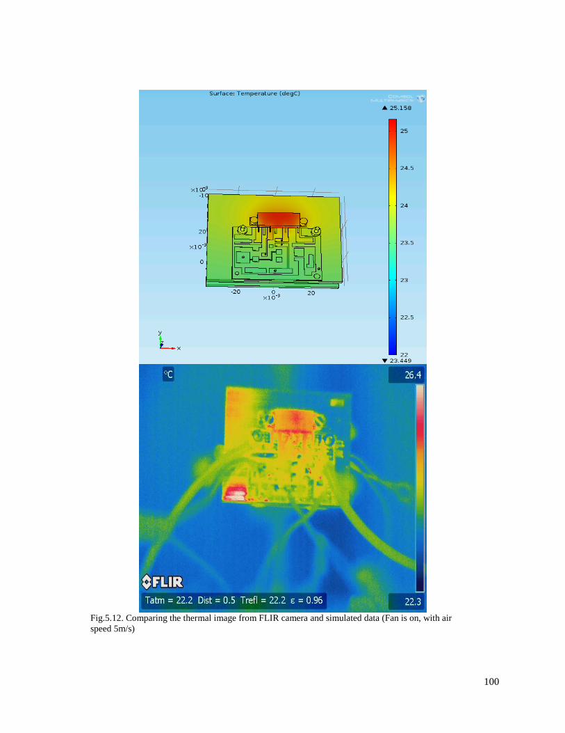
100
Fig.5.12. Comparing the thermal image from FLIR camera and simulated data (Fan is on, with air
speed 5m/s)

101
5.4. Conclusion
In this chapter we presented our lab setup test for measuring the thermal distribution of a RF power
amplifier (7W) by FLIR camera. We also tried to model the structure in our multi-physics cad tools by
using COMSOL 4.4. This model was based on the power delivery of the power transistor.
After comparing two data extracted from measurements and simulation, we achieved a good agreement.
We repeated the test for different scenarios. When the fan is off the maximum temperature measured on
top of the power transistor was 31 C. The simulated data was calculated only 1 degree Celsius lower than
the measured data (which is 30C). For the second try, an air cooling system was applied to heatsink, and
by using a fan with were able to control the speed of air around the structure. After extracting data from
both cases, a very good agreement was observed for the temperature distribution of the power transistor.
Which is around 25C as a maximum temperature. This task was a good example to show how much the
accuracy of our 3D multi-physics model is.

102
CHAPTER 6
Contributions and Future Work
6.1. Introduction
Since developing electronic industry, there has been huge effort to increase the density of transistors in
very tiny region like microchips, to improve the speed of processors and create very large memories for
huge computations processes. With the hardware industry significant improvements, there are many studies
have been carried out in different fields like computer science to look for different techniques to model
such complicated processes using multi-physics CAD tools (based on very complicated mathematical
equations). The goal is to achieve a model that can predict many events with a very precise simulation that
would require massive computational capabilities for mixed multi-physics modeling. For this reason, these
studies are completely dependent on hardware and software limitations.
Each year engineers present many new innovative concepts at conferences that could help researchers to
solve some of these challenges. For around ten years, the speed of processors and the memory capacity are
adequate enough to start looking at some complicated problems that scientists were previously not able to
solve them before---because of the required large amount of computations, and their natural complexities.
For instance, recently modeling multi-physics problems have been invested by many research groups all
over the world to find ways to fill the gap, which is, exist between these different physics problems. In this
work, we have addressed two common challenges: 1- investigating the operation of solar cells and how to
increase their efficiency 2-Thermal analysis of electronic boards and their multi-physics modeling and
failure mechanisms. This is one of the first step in this multi-physics modeling and a long way is still ahead
of us and we would like to point out still open questions.

103
6.2. Contributions
3-D multi-physics modeling for solving some common problems in electrical engineering has been
proposed. Creating a database (based on material properties applied for different physics) is critical step
that needs to be done for initializing the model. In this study, a solar cell was analyzed. Our developed
simulator (based on COMSOL 4.4 and MATLAB) is a real multi-physics modeling toolbox. It can comprise
for three coupled modules: Optics, carrier transport in semiconductors, and Electrostatic. To achieve an
accurate simulated result (compared to measurement), the device was modeled in 3D. For this reason we
were able to accurately predict the electric field distribution due to the light scattering inside and outside of
the device. Also 3D plasmonic particles can be excited by randomly polarized sun light. This 3D tool has
been validated by comparing its results with published measured ones [94]. The comparison between both
measured and simulated data indicates a very good agreement even though some material parameters were
assumed like the dopant distribution, and the density of traps (recombination), in addition to some assumed
layers’ thicknesses.
To approach a good conclusion, many simulations have been done to analyze the plasmon layer’s
behavior (MNP created by small metallic particles). Then we could observe some major phenomena like
strong localized fields around the MNPs. Random embedding of MNPs has resulted in an unexpected
degradation of solar cell efficiency. A significant efficiency drop after adding the MNPs has been related
to the substantial number of defects left after embedding. Presence of these defects has resulted in a
considerable optical loss around the MNPs. Second, a pronounced increase in recombination rates (if
generated free electron-hole pairs were kept at the highly doped region) which would reduce the
conversion of optical energy to photons. Meanwhile, using small MNPs at the top (P+) layer, should
allow a significant portion of the optical energy to propagate through (it acts like a transparent layer for
lower frequencies), and larger MNPs are placed at the bottom to enhance reflection/scattering. It is
certainly not recommended to embed those large MNPs inside the active region, because it can create a

104
large amount of optical loss for the whole system. Simulations indicated an impressive efficiency
enhancement of up to ~30% which amount to 13% overall efficiency [95].
To continue our research, we have investigated on the second problem which is electro-thermal problem
for electronic circuits. Same as the first problem we have tried to recognize different physics involved in
this project. Then we presented a 3D Multi-physics model by using COMSOL 4.4. Our developed multi-
physics models and proposed solver scheme are developed to resolve the electro-thermal problems for
different electronic systems, and definitely could clearly describe how the electric current flowing through
the conductors can cause a voltage drop creating hot spots.
To validate our models, however, we chose different structures that were previously measured and
published and then we compared our simulated data with their measurements.
Finally, we conclude with the following recipe when Joule heating effect due to the current flowing
through conductors is considered.
It needs to create database for electrical resistivity or conductivity as a function of temperature.
The temperature effect on IR drop cannot be neglected. For instance avoiding thermal effect can
cause up to 20% error for IR drop.
The current crowding at hot regions need to be detected. It can be resolved by changing the size of
interconnectors or path lines for dc current.
To transfer the heat to the heatsink efficiently, a good material with right structure (size) need to
be designed.
It is helpful to provide more than one path for the current either by providing parallel plates
connected by VIAs, or multitude of routes connected in a current junction (node). Such current
splitting can significantly reduce the power loss upon reducing the current value in each conductor,
while keeping the overall current of interconnections the same.

105
6.3. Future work in modeling solar cells
In this study, there are some items that we still need to address.
1- Improving material property database. It needs more work to consider new parameters in different
fields by using reliable references.
2- Improving the model of defects created by a plasmon layer for different types of semiconductors.
3- Study of the effect of surface roughness. Since the number of cells increases upon the increase in the
geometry complexity of the structure, we really like to continue this work for different types of
surface roughness, and analyze the effect of surface roughness on harvesting energy at different
regions of the spectrum.
4- Study of the performance of solar cell by considering the heat effect (created by radiation from sun)
Since the temperature of the metallic layer of the solar cells (located at the back) is changed by
environment, then it needs more investigation as a new multi-physics problem to analyze the effect
of heat on material properties of the layers, and also the physical shape of the structure.
5- Study plasmon solar cell performance with the heat effect consideration. At this time, we assume
fixed material properties, but in reality it is function of temperature and should be considered to
improve the modeling accuracy. For example, when we add metallic particles (as plasmon layer) to
improve efficiency, the structure captures more heat from these metallic particles. This event can
change the performance of the device easily. To account for that, we need to develop a new multi-
physics model, which involves thermal modeling as well. For the sake of solving this new multi-
physics problem, a new database of various material properties is needed as a function of temperature
including the semiconductor materials.
6- Finally to create an accurate model for the solar cell, it’s more accurate to consider any physical
changes (like expansion, or deformation” of the tiny metallic part in the electrodes, or also in the
semiconductor regions) as function of temperature of the whole system. This model will require lots

106
of computation and complexity to involve many coupled physics modules (Thermal, Mechanic of the
structures, optics, semiconductor, electricity) as well.
6.4. Future work in modeling electro-thermal problem
In this study, there are some items that we need to address as future work.
1- Model More complex geometries
Since the number of cells is increasing with the increase of structure complexity, we should continue our
work of modeling multi-layered boards with large number of traces for more realistic structures.
2- We need to consider any physical deformation (expansion and compression) in multi-physics
modeling. Which means that the database needs to be updated based on mechanical properties as a
function of temperature. It will increase the complexity of model of course. Changing the physical
size of the structure can affect electrical parameters, and indirectly can affect the temperature of the
whole system.
3- The PDN and cooling system are very critical parts of this study, and it definitely needs more
investigation to apply a special material to the system in critical regions like VIAs for transferring
the heat efficiently without any changes in their physical shape.

107
References
108
[1] Frederik C. Krebs. Polymeric Solar Cells: Materials, Design, Manufacture. DEStech
Publications, Inc., Lancaster, Pennsylvania, 2010.
[2] William Shockley and Hans J. Queisser. Detailed balance limit of efficiency of p-n junction
solar cells. Journal of Applied Physics, 32:510-519, 1961.
[3] M. A. Green, K. Emery, Y. Hishikawa, and W. Warta. Solar cell efficiency tables (version 43).
Progress in Photovoltaics: Research and Applications, 18:346-352, 2010.
[4] M. LoCascio. Application of semiconductor nanocrystals to photovoltaic energy conversion
devices. Evident Technologies, Troy, NY, August 2002.
[5] University of New South Wales
[6]. Zeman M. Advanced Amorphous Silicon Solar Cell Technology, in Thin Film Solar Cells:
Fabrication, Characterization and Applications, eds. Poortmans J, Archipov V. Wiley: Chichester,
2006; 173–236, ISBN: 978-0-470-09126-5.
[7]. H.W.Deckman, C.B.Roxlo, and E.Yablonovitch, "Maximum statisticalincrease of optical
absorption in textured semiconductor films,” Optic Letters, Vol.8, No.9, 1983.
[8]. Isabella O, Moll F, Krč J, Zeman M. Modulated surface textures using zinc-oxide films for
solar cells application. Physica Status Solidi A 2010; 1–5, DOI: 10.1002/pssa.200982828.
[9]. Kambe M, Takahashi A, Taneda N, Masumo K,Oyama T, Sato K. Proceedings of the 33rd
IEEE PVSC: San Diego (IEEE: New York, 2008); 1–4,DOI:10.1109/PVSC.2008.4922507.
[10]. Haug F-J, Söderström T, Cubero O, Terrazzoni-Daudrix V, Niquille X, Perregeaux S, Ballif
C. Materials Research Society Symposium Proceedings 2008; 1101: KK13-KK; DOI:
10.1557/PROC-1101-KK13-01.
[11]. Krč J, Zeman M, Čampa A, Smole F, Topič M. Novel approaches of light management in
thin-film silicon solar cells. Materials Research Society Symposium Proceedings 2006; 910: A25-
A; DOI: 10.1557/ PROC-0910-A25-01.

109
[12] Celine Pahud, Olindo Isabella, Ali Naqavi, Franz-Josef Haug, Miro Zeman, Hans Peter Herzig,
and Christophe Ballif, "Plasmonic silicon solar cells: impact of material quality and geometry",
OSA 2013,Vol. 21, No. S5 | DOI:10.1364/OE.21.00A786
[13].Seyfollah Toroghi and Pieter G. Kik, “Cascaded plasmonic metamaterials for phase-controlled
enhancement of nonlinear absorption and refraction”
[14]. R. Santbergen,R. Liang,and M. Zeman, A-Si:H Solar Cells with embedded silver
Nanoparticles, IEEE 2010.
[15]. H. R. Stuart and D. G. Hall, "Island size effects in nanoparticle-enhanced photodetectors,"
Appl. Phys. Lett.73, 3815 (1998).
[16]. Ulf Malm, MarikaEdoff, "2D devicemodellingandfiniteelementsimulationsforthin-
filmsolarcells", Solar EnergyMaterials&SolarCells93 (2009)1066–1069.
[17]. E. Ihalane*1, M. Meddah1, A. Elfanaoui1, L. Boulkaddat1, E. El hamri1, X. Portier2, A.
Ihlal1 and K.Bouabid, "NUMERICAL SIMULATION OF PHOTOCURRENT IN A SOLAR
CELL BASED AMORPHOUS SILICON",2011.
[18]. Paul A. Basore, "Numerical Modeling of Textured Silicon Solar Cells Using PC-1D", IEEE
transactions on electron devices, Vol. 37, NO. 2. FEB 1990.
[19]. Stefaan Degrave, Marc Burgelman, Peter Nolle “MODELLING OF POLYCRYSTALLINE
THIN FILM SOLAR CELLS:NEW FEATURES IN SCAPS VERSION 2.3,” 3rd World
Conference on Pholovolroic Lnirergv Conversion Mov 11-18,2003 Osaka.Japan
[20]. Marcela Barrera, FranciscoRubinelli, IgnacioRey-Stolle, and JuanPla “Numerical
simulationofGesolarcellsusingD-AMPS-1Dcode,” M. Barreraetal./PhysicaB 407(2012)3282–
3284.
[21]. Olindo Isabella , Serge Solntsev ,and Miro Zeman “3-D optical modeling of thin-film silicon
solar cells on diffraction gratings,” PROGRESS IN PHOTOVOLTAICS: RESEARCH AND
APPLICATIONS, Prog. Photovolt: Res. Appl.2013;21:94108
[22] Xiaofeng Li, Nicholas P. Hylton, Vincenzo Giannini, Kan-Hua Lee, Ned J. EkinsDaukes,
110
and Stefan A. Maier “Bridging electromagnetic and carrier transport calculations for three-
dimensional modelling of plasmonic solar cells ,” 2011 / Vol. 19, No. S4 / OPTICS EXPRESS
A888.
[23]. Michael G. Deceglie, Vivian E. Ferry, A. Paul Alivisatos, and Harry A. Atwater “Design of
Nanostructured Solar Cells Using Coupled Optical and Electrical Modeling,”
doi.org/10.1021/nl300483y Nano Lett. 2012, 12, 2894−2900
[24]. Yee KS. Numerical solution of initial boundary value problems involving Maxwell’s
equations. IEEE Transactions on Antennas and Propagation 1966; 14 : 302–307.
[25]. Weiland T. A discretization method for the solution of Maxwell’s equations for six-
component fields. Electronics and Communications AEUE 1977; 31(3):116–120.
[26]. Moharam MG, Gaylord TK. Rigorous coupled-wave analysis of planar-grating diffraction.
Journal of the Optical Society of America 1981; 71: 811–818.
[27]. Gibson WC. The Method of Moments in Electromagnetics. Chapman & Hall/CRC: Boca
Raton, 2008; ISBN 978-1-4200-6145-1.
[28]. Jin J-M. The Finite Element Method in Electromagnetics.2nd ed. John Wiley & Sons: New
York, 2002; ISBN: 978-0-471-43818-2.
[29]. Xunming Deng and Eric A. Schiff, Amorphous Silicon–based Solar Cells, chapter 12
[30]. NABEEL A BAKR1, A M FUNDE1, V S WAMAN1, M M KAMBLE1,R R HAWALDAR2,
D P AMALNERKAR2, S W GOSAVI3 and S R JADKAR3, "Determination of the optical
parameters of a-Si:H thin films deposited by hot wire–chemical vapor deposition technique using
transmission spectrum only",2010
[31]. J. A. Alamo and R. M. Swanson, "Modeling of minority-carrier transport in heavily doped
silicon emitters" Solid-State Electronics Vol.30,No. 11,pp. 1127-1136,1987.
[32]. J Piprek, Semiconductor optoelectronic devices introduction to physics and simulation, 2003.
[33]. I. Sakata and Y. Hayashi, "Theoretical Analysis of Trapping and Recombination of Photo
generated Carriers in Amorphous Silicon Solar Cells", Appl. Phys. A 37, 153-164 (1985).
111
[34]. SZE, Physics of semiconductor Devices, 2nd Edition, 1981
[35]. Donald A.Neamen, Semiconductor Physics and Devices: Basic Principles, 3rd edition
[36]. Otfried Madelung, Semiconductors: Data Handbook, Springer
[37]. John J. Quinn, Kyung-Soo Yi, Solid State Physics: Principles and Modern Applications,
Springer, 2009
[38]. P. B. Johnson and R. W. Christy, “Optical constants of the noble metals”, phys. Rev. letters
11. 541 (1963)
[39]. OptiFDTD: Technical Background and Tutorials.
[40]. Terrestrial photovoltaics measurement procedures, NASA Tech. Memo. TM 73702, National
Aeronautics and Space Administration, Cleveland, OH, 1977.
[41]. http://www.astm.org/Standards/G159.htm
[42]. Rahul Dewan, Stefan Fischer, V Benno Meyer-Rochow, Yasemin O¨ zdemir, Saeed Hamraz
and Dietmar Knipp, "Studying nanostructured nipple arrays of moth eye facets helps to design
better thin film solar cells" , Bioinspir. Biomim. 7 (2012) 016003 (8pp)
[43]. M. Gracia., F. Rojas, and G. Gordillo, "MORPHOLOGICAL AND OPTICAL
CHARACTERIZATION OF SnO2:F THIN FILMS DEPOSITED BY SPRAY PYROLYSIS,"
20th European Photovoltaic Solar Energy Conference, 6 –10 June 2005, Barcelona, Spain
[44]. Adib Abou Chaaya, Roman Viter, Mikhael Bechelany, Zanda Alute, Donats Erts, Anastasiya
Zalesskaya ,Kristaps Kovalevskis, Vincent Rouessac, Valentyn Smyntyna and Philippe Miele,
"Evolution of microstructure and related optical properties of ZnO grown by atomic layer
depsition" Beilstein J. Nanotechnol. 2013, 4, 690–698 doi:10.3762/bjnano.4.78
[45]. Vinod Kumar, Neetu Singh, R. M. Mehra, Avinashi Kapoor, L.P. Purohit, H.C. Swart "Role
of film thickness on the properties of ZnO thin films grown by sol-gel method," ELSEVIER Thin
Solid Films 539 (2013) 161–165
[46]. C.A. Balanis, Advanced Engineering Electromagnetics, Wiley, 1989.
112
[47]. A. L. Aden, “Scattering from spheres with sizes comparable to the wavelength,” J. Appl.
Phys., vol. 12, 1951.
[48]. Pierce, D. T.; Spicer, W. E "Electronic Structure of Amorphous Si from Photoemission and
Optical Studies," Pierce, Spicer (1972) Phys. Rev. B 5, 3017.
[49] C. Hu, “MOSFET Scaling in the Next Decade and Beyond,” Semiconductor International, pp.
105-114, 1994.
[50] K. C. Saraswat and F. Mohammadi, “Effect of Interconnection Scaling on Time Delay of VLSI
Circuits,” IEEE Trans. On Electron Devices, vol. ED-29, pp. 645- 650, 1982.
[51] M. T. Bohr and Y. A. El-Mansy, "Technology for Advanced High-Performance
Microprocessors," IEEE Trans. Electron Devices, vol 45, no. 3, pp. 620-625, 1998.
[52] T. N. Theis, “The Future of Interconnection Technology”, IBM Journal of R&D, Vol. 44,
2000.
[53] R. Ho, K. Mai, and M. Horowitz, “The Future of Wires,” Proceedings of the IEEE, vol.89,
no.4, pp. 490-504, April 2001.
[54] S. Venkatesan, A. V. Gelatos, S. Hisra, B. Smith, R. Islam, J. Cope, B. Wilson, D. Tuttle, R.
Cardwell, S. Anderson, M. Angyal, R. Bajaj, C. Capasso, P. Crabtree, S. Das, J. Farkas, S. Filipiak,
B. Fiordalice, M. Freeman, P. V. Gilbert, “A High Performance 1.8V, 0.20 µm CMOS Technology
with Copper Metallization,” IEDM Tech. Dig., pp. 769-772, 1997.
[55] F. Pollack, “New Challenges in Microarchitecture and Compiler Design”, PACT 2000, Oct
2000.
[56] P. K. Ko, “Hot-Electron Effects in MOSFET’s,” Ph.D. dissertation, Univ. of California,
Berkeley, 1982.
[57] C. Fiegna, H. Iwai, T. Wada, T. Saito, E. Sangiorgi, and B. Ricco, “Scaling the MOS Transistor
below 0.1 µm: Methodology, Device Structure, and Technology Requirements,” IEEE Trans.
Electron Devices, vol. 41, no. 6, p. 941, June 1994.
113
[58] L. Jiang, S. Kolluri, B. J. Rubin, H. Smith, E. G. Colgan, M. R. Scheuermann, J. A. Wakil, A.
Deutsch, and J. Gill, "Thermal Modeling of On-Chip Interconnects and 3D Packaging Using EM
Tools", IEEE Conference on Electrical Performance of Electronic Packaging (EPEP), 2008.
[59] J.D. Wu, P.J. Zheng, C.W. Lee, S.C. Hung and J.J. Lee, A study in flip chip UBM/bump
reliability with effects of SnPb solder composition, Microelectron Reliab 46 (2006), pp. 41–52.
[60] W. Dauksher, D. H. Eaton, and J. D. Rowatt,,”A Finite-Element-Based Methodology for
Evaluating Solder Electromigration Current Limits of Sn/Pb Eutectic Solder Bumps”, IEEE
TRANSACTIONS ON DEVICE AND MATERIALS RELIABILITY, VOL. 8, NO. 1, MARCH
2008.
[61] Y. Li, Q. S. Zhang, H. Z. Huang, and B. Y. Wu, “Simulation of Effect of Current Stressing
on Reliability of Solder Joints with Cu-Pillar Bumps”, World Academy of Science, Engineering
and Technology 61 2010.
[62] Yi-Shao Lai , Chin-Li Kao, “Electrothermal coupling analysis of current crowding and Joule
heating in flip-chip packages”, Microelectronics Reliability 46 (2006) 1357–1368.
[63] B. Vermeersch, G. De Mey, “Device level electrothermal analysis of integrated resistors,”
14th International Conference on Mixed Design of Integrated Circuits and Systems, pp. 375-380,
Jun. 2007.
[64] Peng Li, L. T. Pileggi, M. Asheghi, R. Chandra, “Efficient full-chip thermal modeling and
analysis,” IEEE/ACM International Conference on Computer Aided Design (ICCAD), pp. 319-
326, Nov. 2004.
[65] J Xie, D. Chung, M. Swaminathan, M. Mcallister, A. Deutsch, L. Jiang and B. J. Rubin
“Electrical-thermal co-analysis for power delivery networks in 3D system integration”, IEEE
International Conference on 3D System Integration - 3DIC, pp.1-4, 2009.
[66] Y. S. Lai and C. L. Kao “Electro-thermal coupling analysis of current crowding and Joule
heating in flip-chip packages”, Elsevier Microelectronics Reliability 46 (2006) 1357–1368.
114
[67] L. N. Ramanathan, J. W. Jang, J. Tang and D.R. Frear “Electromigration Behavior of Flip-
Chip Solder Bumps Subjected to RF Stressing”, Electronic Components and Technology
Conference, ECTC 2008. 58th;978-1-4244-2231, 2008.
[68] W. Dauksher, D. H. Eaton and J. D. Rowatt, "A Finite-Element-Based Methodology for
Evaluating Solder Electromigration Current Limits of Sn/Pb Eutectic Solder Bumps", IEEE
TRANSACTIONS ON DEVICE AND MATERIALS RELIABILITY, VOL. 8, NO. 1, MARCH
2008.
[69] V. Nagaraj "FLIP CHIP BACK END DESIGN PARAMETERS TO REDUCE BUMP
ELECTROMIGRATION", 2008.
[70] http://www.developers.net
[71] M. Salleras Freixes "THERMAL MODELING OF MICROSYSTEMS AND ELECTRONIC
COMPONENTS:MODEL ORDER REDUCTION", 2003.
[72] R. Schmidt, “Liquid cooling is back”, Electronics Cooling, vol. 11 (3), (2005).
[73] R.E. Simons, “The Evolution of IBM High Performance Cooling Technology,” IEEE Trans.
Comp. Pack. Manuf. Tech. A, vol. 18 (4), pp. 805-811, (1995).
[74] J. Black, “Physics of Electromigration,” IEEE International Reliability Physics Symposium,
142 (1974).
[75] Black J., “Mass Transport of Aluminum by Momentum Exchange with Conducting
Electrons”, 6th Annual Reliability Physics Symposium, Los Angeles, November, 1967, pp. 148-
159.
[76] L.T. Yeh, “Review of Heat Transfer Technologies in Electronic Equipment,” Journal of
Electronic Packaging, vol. 117, pp. 333-339, (1995).
[77] Zhao J. H., “Theoretical and experimental study of electromigration,” in Electromigration &
Electronic Device Degradation, A. Christou, ed., John Wiley & Sons, New York (1994), Chpt. 6.
[78] Hsiang-Chen Hsu, Shen-Wen Ju, Jie-Rong Lu, Hong-Shen Chang, Hong-Hau Wu,
"Electromigration Analysis and Electro-Thermo-Mechanical Design for Semiconductor Package",
115
International Conference on Electronic Packaging Technology & High Density Packaging (ICEPT-
HDP)IEEE, 2009.
[79] Flip Chip Packaging Technology, Amkor, 2006. www.amkor.com
[80] Package Portfolio for Intel’s Flash Memory Products, Intel Corporation, 2005.
[81] Product Manual, Advanced Semiconductor Engineering Corporation.
[82] Product Manual, Sony Incorporation.
[83] Bump Design Guideline, Flip Chip International, 2006.
[84] Vincent Fiori, Sebastien Gallois-Garreignot, Clement Tavernier, Herve Jaouen, Andre Juge
"Chip-Package Interactions: Some Combined Package Effects on Copper/Low-k Interconnect
Delaminations", IEEE, 2008.
[85] K. M. Chen and T. S. Lin "Copper pillar bump design optimization for lead free flip-chip
packaging" Springer, 2009.
[86] Agarwala B. N., Attardo M. J., and Ingraham A. J., “Dependence of Electromigration-Induced
Failure Time on Length and Width of Aluminum Thin Film Conductors,” J. of Applied Physics,
Vol. 41, September, 1970, pp. 3954-3960.
[87] Cho J. and Thompson C. V., “Grain Size Dependence of Electromigration-Induced Failures in
Narrow Interconnects,” Applied Physics Letters, Vol. 54, No. 25, June, 19, 1989, pp. 2577-2579.
[88] Guotao Wang, Paul S. Ho, and Steven Groothuis "Chip-packaging interaction: a critical
concern for Cu/low k packaging" Elsevier, 2004.
[89] Rathin Mandal and Y.C.Mui "Copper-Pillar Bump-Joint Thermo-Mechanical and Thermal
Modeling for Flip-Chip Packages",IEEE Electronics Packaging Technology Conference, 2008.
[90] Tyler Osborn, C. Hunter Lightsey, Paul A. Kohl "Low-k compatible all-copper flip-chip
connections" Elsevier 2008.
[91] Young-Joon Lee and Sung Kyu Lim "Co-Optimization of Signal, Power, and Thermal
Distribution Networks for 3D ICs", IEEE Electrical Design of Advanced Packaging and Systems
Symposium, 2008.
116
[92] Y. Zhan, B. Goplen, and S. S. Sapatnekar, “Electrothermal analysis and optimization
techniques for nanoscale integrated circuits,” Asia and South Pacific Conference on Design
Automation, pp. 219-222, Jan. 2006.
[93] K. Fukahori, P. R. Gray, “Computer simulation of integrated circuits in the presence of
electrothermal interaction,” IEEE Journal of Solid-State Circuits, vol. 11, no. 6, pp. 834-846, Dec.
1976.
[94] Ahmadreza Ghahremani and Aly E. Fathy "A three-dimensional multiphysics modeling of
thin-film amorphous silicon solar cells", Energy Science & Engineering 2015.
[95] Ahmadreza Ghahremani and Aly E. Fathy "Strategies for Designing High Efficient Thin-Film
Amorphous Silicon Solar Cells ", IEEE 2015.

117
Appendix
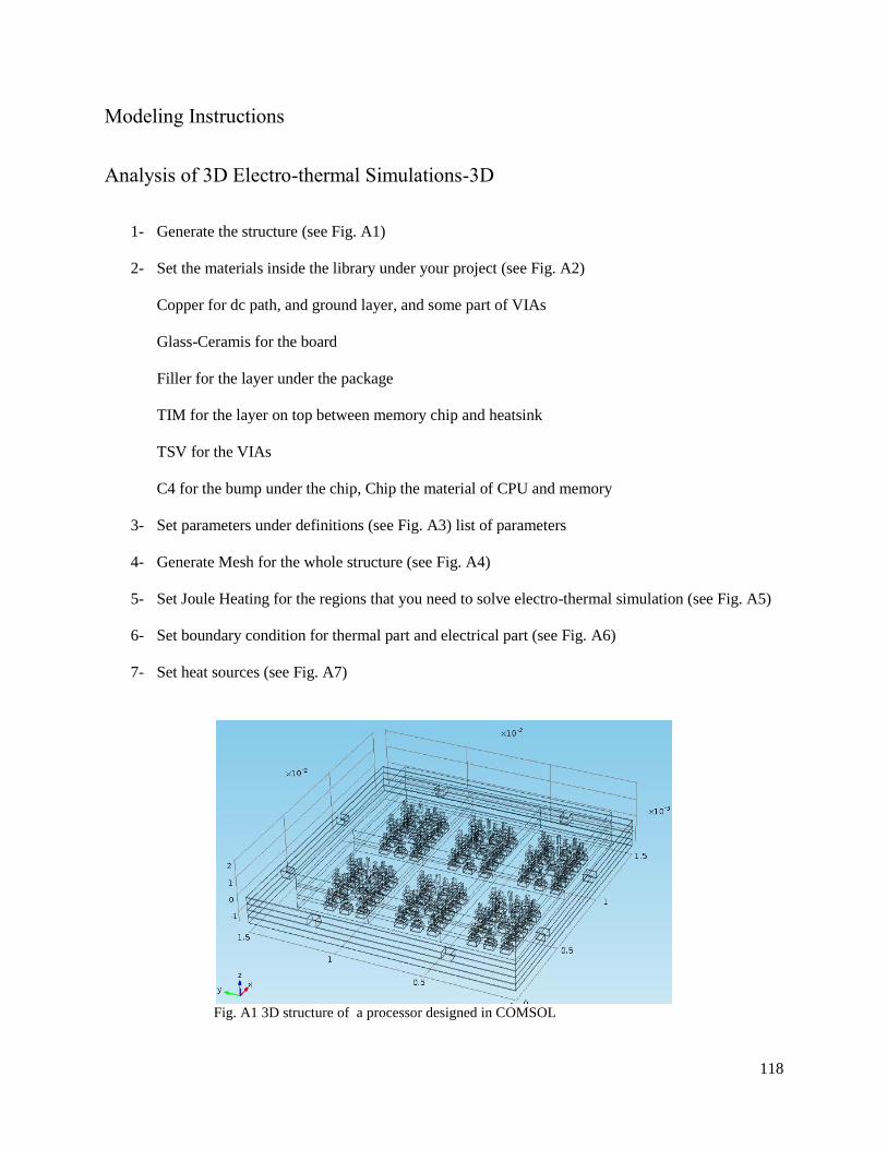
118
Modeling Instructions
Analysis of 3D Electro-thermal Simulations-3D
1- Generate the structure (see Fig. A1)
2- Set the materials inside the library under your project (see Fig. A2)
Copper for dc path, and ground layer, and some part of VIAs
Glass-Ceramis for the board
Filler for the layer under the package
TIM for the layer on top between memory chip and heatsink
TSV for the VIAs
C4 for the bump under the chip, Chip the material of CPU and memory
3- Set parameters under definitions (see Fig. A3) list of parameters
4- Generate Mesh for the whole structure (see Fig. A4)
5- Set Joule Heating for the regions that you need to solve electro-thermal simulation (see Fig. A5)
6- Set boundary condition for thermal part and electrical part (see Fig. A6)
7- Set heat sources (see Fig. A7)
Fig. A1 3D structure of a processor designed in COMSOL
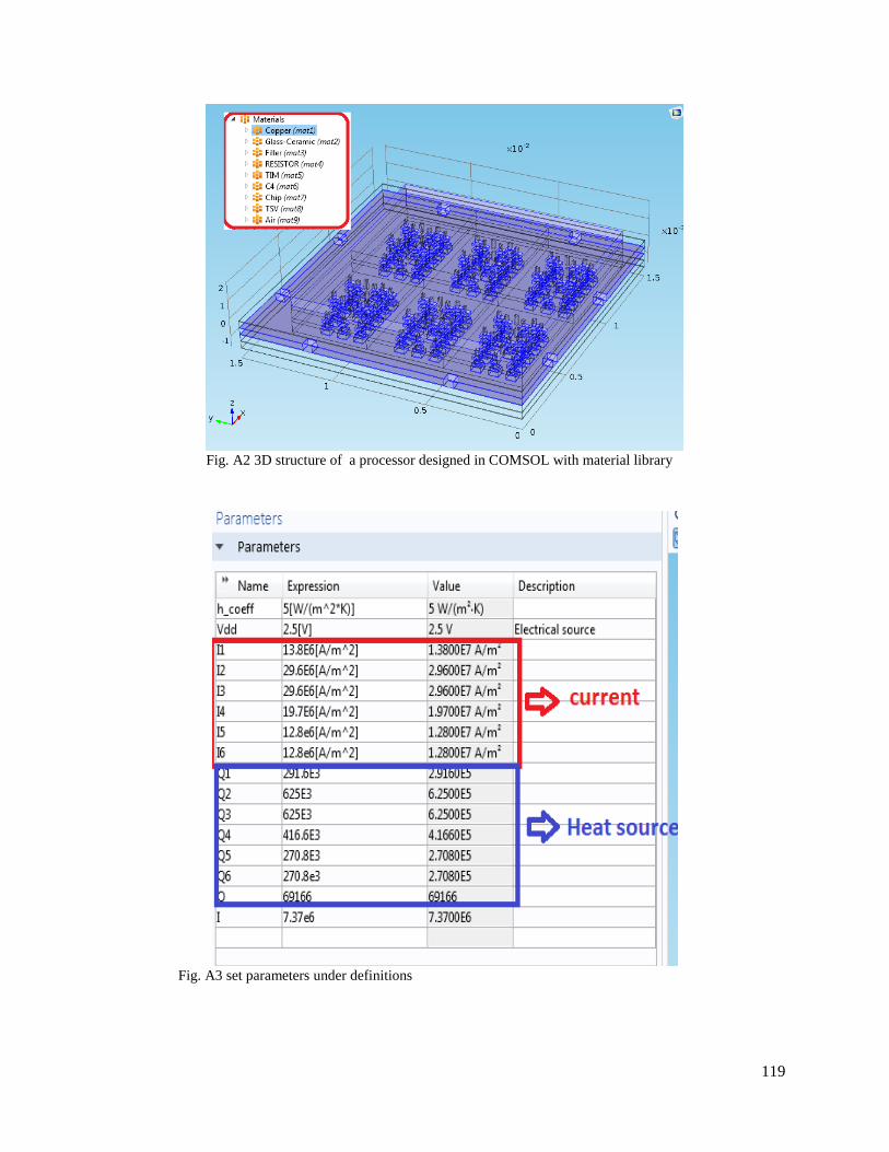
119
Fig. A2 3D structure of a processor designed in COMSOL with material library
Fig. A3 set parameters under definitions
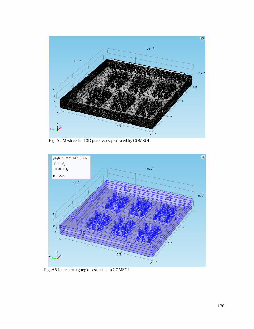
120
Fig. A4 Mesh cells of 3D processors generated by COMSOL
Fig. A5 Joule heating regions selected in COMSOL
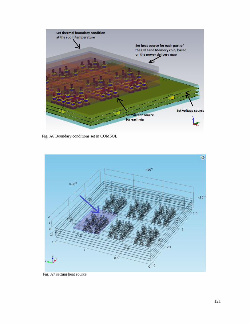
121
Fig. A6 Boundary conditions set in COMSOL
Fig. A7 setting heat source

122
As an example we describe a simple example for an only one heat source located beside power delivery
system, and we listed the steps that need to be done to solve this electro-thermal problem.
Modeling Instructions
From the File menu, choose New.
NEW
1 In the New window, click Model Wizard.
MODEL WIZARD
1 In the Model Wizard window, click 3D.
2 In the Select physics tree, select Heat Transfer>Electromagnetic Heating>Joule Heating.
3 Click Add.
4 Click Study.
5 In the Select study tree, select Preset Studies for Selected Physics Interfaces>Stationary.
6 Click Done.
GEOMETRY 1
Import 1 (imp1)
1 On the Home toolbar, click Import.
2 In the Settings window for Import, locate the Import section.
3 Click Browse.
GLOBALDEFINITIONS
Parameters
1 On the Home toolbar, click Parameters.
2 In the Settings window for Parameters, locate the Parameters section.
3 In the table, enter the following settings
ADD MATERIAL
1 On the Home toolbar, click Add Material to open the Add Material window.
2 Go to the Add Material window.
3 In the tree, select Built-In>Copper.
Name Expression Value Description
j_CE 1e5[A/m^2] 1E5 A/m² Current density,
collector and emitter
routes
Q_h 1e5[W/m^2] 1E5 W/m² Boundary heat source
strength
h_coeff 5[W/(m^2*K)] 5 W/(m²·K) Heat transfer
coefficient
4 Click Add to Component in the window toolbar.
ADD MATERIAL

123
1 Go to the Add Material window.
2 In the tree, select Built-In>FR4 (Circuit Board).
3 Click Add to Component in the window toolbar.
ADD MATERIAL
1 Go to the Add Material window.
2 In the tree, select Built-In>Silica glass.
3 Click Add to Component in the window toolbar.
ADD MATERIAL
1 Go to the Add Material window.
2 In the tree, select Built-In>Solder, 60Sn-40Pb.
3 Click Add to Component in the window toolbar.
MATERIAL
Solder, 60Sn-40Pb (mat4)
On the Home toolbar, click Add Material to close the Add Material window.
Copper (mat1)
1 Click the Wireframe Rendering button on the Graphics toolbar.
2 In the Model Builder window, under Component 1 (comp1)>Materials click Copper
(mat1).
3 In the Settings window for Material, locate the Geometric Entity Selection section.
4 Click Clear Selection.
5 Select Domains 2–4 and 9–12 only
.
FR4 (Circuit Board) (mat2)
1 In the Model Builder window, under Component 1 (comp1)>Materials click FR4 (Circuit
Board) (mat2).
2 Select Domain 1 only.
Silica glass (mat3)
1 In the Model Builder window, under Component 1 (comp1)>Materials click Silica glass
(mat3).
Solved with COMSOL Multiphysics 5.2
8 | POWE R TR A NS I S TOR
2 Select Domain 7 only.
Solder, 60Sn-40Pb (mat4)
1 In the Model Builder window, under Component 1 (comp1)>Materials click Solder,
60Sn-40Pb (mat4).
2 Select Domains 5, 6, and 8 only.
3 In the Settings window for Material, locate the Material Contents section.
4 In the table, enter the following settings:
ELECTRICCURRENTS ( EC )
1 In the Model Builder window, under Component 1 (comp1) click Electric Currents (ec).
2 Select Domains 2–6 and 8–11 only.

124
Ground 1
1 On the Physics toolbar, click Boundaries and choose Ground.
2 Select Boundaries 69, 87, and 105 only.
Normal Current Density 1
1 On the Physics toolbar, click Boundaries and choose Normal Current Density.
2 Select Boundary 10 only.
3 In the Settings window for Normal Current Density, locate the Normal Current
Density section.
4 In the Jn text field, type j_CE.
Normal Current Density 2
1 On the Physics toolbar, click Boundaries and choose Normal Current Density.
2 Select Boundary 5 only.
3 In the Settings window for Normal Current Density, locate the Normal Current
Density section.
4 In the Jn text field, type -j_CE.
Normal Current Density 3
1 On the Physics toolbar, click Boundaries and choose Normal Current Density.
2 Select Boundary 15 only.
Property Name Value Unit Property group
Relative permittivity epsilonr 1 1 Basic
3 In the Settings window for Normal Current Density, locate the Normal Current
Density section.
4 In the Jn text field, type 1e-3*j_CE.
In the Model Builder window, under Component 1 (comp1) click Heat Transfer in Solids
(ht).
Heat Flux 1
1 On the Physics toolbar, click Boundaries and choose Heat Flux.
2 In the Settings window for Heat Flux, locate the Boundary Selection section.
3 From the Selection list, choose All boundaries.
4 Locate the Heat Flux section. Click the Convective heat flux button.
5 In the h text field, type h_coeff.
Boundary Heat Source 1
1 On the Physics toolbar, click Boundaries and choose Boundary Heat Source.
2 Select Boundary 142 only.
3 In the Settings window for Boundary Heat Source, locate the Boundary Heat Source
section.
4 In the Qb text field, type Q_h.
MESH 1
Free Tetrahedral 1
1 In the Model Builder window, under Component 1 (comp1) right-click Mesh 1 and
choose Free Tetrahedral.
2 Right-click Free Tetrahedral 1 and choose Build All.
125
Vita
Ahmadreza Ghahremani (Reza) received his B.S. degree in the major of Electrical Engineering from
Semnan University, Iran in 2002. Reza received his M.S. degree from K.N. Toosi University of
Technology, Tehran, Iran in the major of Field and Electromagnetic in 2005 where he received the honor
award for achieving the first highest total GPA from the graduate school. Reza graduated as a PhD student
in August 2016 from the department of electrical engineering and computer Science, the University of
Tennessee, Knoxville, USA. His major field is electromagnetic theory. He has done many projects in multi-
physics modeling in optics (like fiber optics), electromagnetic wave propagation, and physics of electronic
devices, electro-thermal, and electrostatics. His research interest are Nanotechnology in Photovoltaics, RF-
Microwave circuits, and Electro-thermal Multi-physics modeling. Also he has done several projects during
his research for designing different types of antennas.