multi-objective 3d floorplanning with integrated voltage
TRANSCRIPT

22
Multi-Objective 3D Floorplanning with Integrated VoltageAssignment
JOHANN KNECHTEL, Masdar Institute, Khalifa University of Science and TechnologyJENS LIENIG, TU DresdenIBRAHIM (ABE) M. ELFADEL, Masdar Institute, Khalifa University of Science and Technology
Voltage assignment is a well-known technique for circuit design, and it has been applied successfully toreduce power consumption in classical 2D integrated circuits (ICs). Its usage in the context of 3D ICs hasnot been fully explored yet although reducing power in 3D designs is of crucial importance, e.g., to tacklethe ever-present challenge of thermal management. In this paper, we investigate the effective and efficientpartitioning of 3D designs into multiple voltage domains during the floorplanning step of physical design.In particular, we introduce, implement, and evaluate novel algorithms for effective integration of voltageassignment into the inner floorplanning loops. Our algorithms are compatible not only with the traditionalobjectives of 2D floorplanning but also with the additional objectives and constraints of 3D designs, includingthe planning of through-silicon vias (TSVs) and the thermal management of stacked dies. We test our 3Dfloorplanner extensively on the GSRC benchmarks as well as on an augmented version of the IBM-HB+benchmarks. The 3D floorplans are shown to achieve effective trade-offs for power and delays throughoutdifferent configurations—our results surpass naive low-power and high-performance voltage assignment by17% and 10% on average. Finally, we release our 3D floorplanning framework as open-source code.
CCS Concepts: •Hardware→ 3D integrated circuits;Chip-level power issues; Partitioning and floor-planning; Thermal issues; Timing analysis;
Additional Key Words and Phrases: voltage assignment, power-performance optimization
ACM Reference Format:Johann Knechtel, Jens Lienig, and Ibrahim (Abe) M. Elfadel. 2017. Multi-Objective 3D Floorplanning withIntegrated Voltage Assignment. ACM Trans. Des. Autom. Electron. Syst. 23, 2, Article 22 (November 2017),25 pages.https://doi.org/10.1145/3149817
1 INTRODUCTIONPower delivery and thermal management are far more critical and challenging for three-dimensionalintegrated circuits (3D ICs) than for 2D ICs [10, 18]. Thus, technological as well as physical-designmeasures to reduce power and accordingly induced heat are much sought-after for the design of3D ICs [10, 14]. Reducing power while maintaining performance has been successfully achievedfor 2D ICs, e.g., by means of voltage assignment (VA) during floorplanning [7, 21, 22, 31] or duringplacement [27, 28]. The key principle of VA is to assign modules to voltage domains such thatpower is optimized yet performance is not deteriorated. The determination of voltage domains and
Author’s addresses: J. Knechtel, (Current address) New York University Abu Dhabi (NYUAD, nyuad.nyu.edu), PO Box 129188,Abu Dhabi, UAE, email: [email protected]; J. Lienig, Institute of Electromechanical and Electronic Design (IFTE, ifte.de), TUDresden, 01062 Dresden, Germany, email: [email protected]; I. M. Elfadel, Masdar Institute, Khalifa University ofScience and Technology (MI, KUSTAR, masdar.ac.ae), PO Box 54224, Abu Dhabi, UAE, email: [email protected].© 2017 Association for Computing Machinery.This is the author’s version of the work. It is posted here for your personal use. Not for redistribution. The definitive Versionof Record was published in ACM Transactions on Design Automation of Electronic Systems, https://doi.org/10.1145/3149817.
ACM Transactions on Design Automation of Electronic Systems, Vol. 23, No. 2, Article 22. Publication date: November 2017.

22:2 Johann Knechtel, Jens Lienig, and Ibrahim (Abe) M. Elfadel
the optimal assignment of modules to these domains are computationally challenging since, inprinciple, a combinatorial assignment problem has to be solved.
Although 3D integration has been identified early on as a practical and promising approach forhigh-performance and power-efficient systems [5], the potential of VA has not been sufficientlyexplored in that context. Lim [19] argued rightly that fast but accurate evaluation and optimizationof the thermal, power and performance criteria, among others, are yet to be handled adequatelyduring 3D floorplanning. Floorplanning itself is acknowledged as a crucial stage for the successfulphysical design of 3D ICs [14, 18]. To the best of our knowledge, Lin et al. [6, 20] were the firstto propose a 3D floorplanner which simultaneously accounts for power consumption, timingand thermal management. However, their work has notable restrictions, including the following:omission of the challenging but essential fixed-outline constraint [1]; over-emphasis of planningfor power/ground through-silicon vias (TSVs) and the omission of signal TSVs; limitation to theMCNC benchmarks, which are too small for 3D integration [15]; and, most hindering, the useof computationally-expensive integer linear programming for voltage assignment as well as RC-network-based analysis for thermal management. Lee et al. [16] approached voltage assignmentfor 3D ICs as post-floorplanning problem, while considering both power optimization and thermalmanagement but neglecting any timing constraints. Their approach is computationally prohibitiveas well; it requires several seconds for a single iteration on small-scale benchmarks. Recently, Wanget al. [34] proposed a voltage-aware design flow, but with dedicated focus on application-specificnetwork-on-chip (NoC) architectures and 3D multi-core chips.In this work, we aim for effective and efficient VA along with its seamless integration into
multi-objective floorplanning for 3D ICs. We make the following contributions:
(1) We propose an integrated VA stage, tailored for the innermost optimization loops of anymodular 3D floorplanning tool (Secs. 2–4). That is, for the first time, we enable the early,effective, and comprehensive design-space evaluation of up-and-coming 3D ICs in termsof power and performance, among other criteria. We also implement our approach into acompetitive, open-source 3D floorplanner.
(2) We present novel, computationally-efficient concepts and techniques for integrated VA.Specifically, we propose novel bottom-up merging and top-down selection phases of voltagedomains (Secs. 4.4 and 4.5). The related algorithms are based on pruning and branch-and-bound techniques. Further concepts include the grouping of modules based on contiguityanalysis (Sec. 4.1) and timing-driven determination of applicable voltages (Secs. 4.2 and 4.3).Our techniques and implementation are made available as open-source software [13].
(3) We conduct extensive experimental studies on the GSRC [8] and IBM-HB+ benchmarksuites [25] (Sec. 6). For the latter, we are the first to define and consider power values. Thus,we enable for the first time power-aware floorplanning for those large-scale benchmarks; weare making these augmented benchmarks publicly available [13]. We reference our novelvoltage-aware floorplanning methodology to the competitive baseline of timing-optimizedfloorplanning, and we compare it to prior art. Furthermore, we elaborate on general findingsfor multi-objective 3D floorplanning for small- and large-scale benchmarks, and we providecorresponding design guidelines.
2 PROBLEM FORMULATION AND OUR FLOORPLANNING METHODOLOGYThe problem of voltage assignment (VA) during 3D floorplanning can be stated as follows: for anygiven 3D floorplan, find its cost-optimal partitioning into voltage volumes along with the resultingvoltage, power and timing assignments for all modules. By definition [Sec. 3-(4)], a voltage volumerepresents the generalized 3D case of a voltage domain/island. Consequently, voltage volumes can
ACM Transactions on Design Automation of Electronic Systems, Vol. 23, No. 2, Article 22. Publication date: November 2017.
Multi-Objective 3D Floorplanning with Integrated Voltage Assignment 22:3
VoltageVolumes:
0.8 V
1.2 V
1.0 V
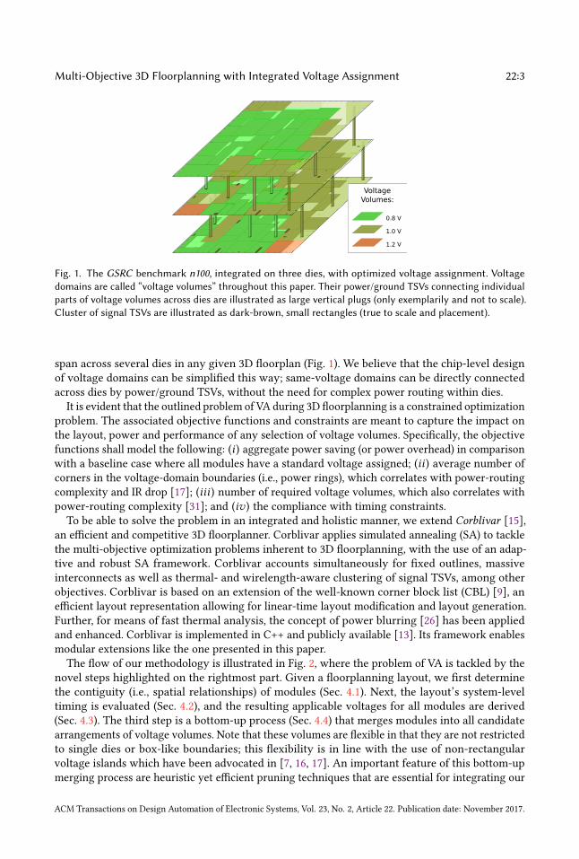
Fig. 1. The GSRC benchmark n100, integrated on three dies, with optimized voltage assignment. Voltagedomains are called “voltage volumes” throughout this paper. Their power/ground TSVs connecting individualparts of voltage volumes across dies are illustrated as large vertical plugs (only exemplarily and not to scale).Cluster of signal TSVs are illustrated as dark-brown, small rectangles (true to scale and placement).
span across several dies in any given 3D floorplan (Fig. 1). We believe that the chip-level designof voltage domains can be simplified this way; same-voltage domains can be directly connectedacross dies by power/ground TSVs, without the need for complex power routing within dies.
It is evident that the outlined problem of VA during 3D floorplanning is a constrained optimizationproblem. The associated objective functions and constraints are meant to capture the impact onthe layout, power and performance of any selection of voltage volumes. Specifically, the objectivefunctions shall model the following: (i ) aggregate power saving (or power overhead) in comparisonwith a baseline case where all modules have a standard voltage assigned; (ii ) average number ofcorners in the voltage-domain boundaries (i.e., power rings), which correlates with power-routingcomplexity and IR drop [17]; (iii ) number of required voltage volumes, which also correlates withpower-routing complexity [31]; and (iv ) the compliance with timing constraints.To be able to solve the problem in an integrated and holistic manner, we extend Corblivar [15],
an efficient and competitive 3D floorplanner. Corblivar applies simulated annealing (SA) to tacklethe multi-objective optimization problems inherent to 3D floorplanning, with the use of an adap-tive and robust SA framework. Corblivar accounts simultaneously for fixed outlines, massiveinterconnects as well as thermal- and wirelength-aware clustering of signal TSVs, among otherobjectives. Corblivar is based on an extension of the well-known corner block list (CBL) [9], anefficient layout representation allowing for linear-time layout modification and layout generation.Further, for means of fast thermal analysis, the concept of power blurring [26] has been appliedand enhanced. Corblivar is implemented in C++ and publicly available [13]. Its framework enablesmodular extensions like the one presented in this paper.The flow of our methodology is illustrated in Fig. 2, where the problem of VA is tackled by the
novel steps highlighted on the rightmost part. Given a floorplanning layout, we first determinethe contiguity (i.e., spatial relationships) of modules (Sec. 4.1). Next, the layout’s system-leveltiming is evaluated (Sec. 4.2), and the resulting applicable voltages for all modules are derived(Sec. 4.3). The third step is a bottom-up process (Sec. 4.4) that merges modules into all candidatearrangements of voltage volumes. Note that these volumes are flexible in that they are not restrictedto single dies or box-like boundaries; this flexibility is in line with the use of non-rectangularvoltage islands which have been advocated in [7, 16, 17]. An important feature of this bottom-upmerging process are heuristic yet efficient pruning techniques that are essential for integrating our
ACM Transactions on Design Automation of Electronic Systems, Vol. 23, No. 2, Article 22. Publication date: November 2017.

22:4 Johann Knechtel, Jens Lienig, and Ibrahim (Abe) M. Elfadel
EvaluateSystem-LevelTiming Paths
DeriveApplicableVoltages
Bottom-UpMerging Phase
Top-DownSelection Phase
IntegratedVoltage Assignment
ContiguityAnalysis
Sec. 4.1
Sec. 4.2
Sec. 4.3
Sec. 4.4
Sec. 4.5Optimized
3D Floorplan
Done ?
Yes
No
Cluster andPlace TSVs
EvaluateInterconnects
EvaluateThermal
Distribution
Evaluate OverallQuality of
Current Solution
GenerateLayout
AdaptSolution
3D Floorplanning Inputs:Netlist, Modules,Technology Setup
3D Floorplaner:Corblivar
Fig. 2. Flow of our extended floorplanning methodology. The novel steps for the integrated voltage assignmentare highlighted on the right. Besides the netlist with all its modules as input, we also require the technologysetup which captures the fixed die outlines, the TSV dimensions, baseline power values for modules, supplyvoltages, etc. See also Sec. 6 and our floorplanning suite [13] for details.
approach into Corblivar’s inner loop without prohibitively increasing the computational efforts.1Finally, a top-down process (Sec. 4.5) selects the best subset of voltage volumes while still satisfyingconstraints such as fixed outlines and critical delays.In order to evaluate any (intermediate or final) floorplanning solution with respect to VA, we
integrate a voltage-assignment cost CVA into Corblivar’s modular framework:
CVA = α1/
∑CMbest
PS ′(cm)
1/∑CMinit PS
′(cm)+ β
avgCMbest(CR (cm))
avgCMinit(CR (cm))
+ γ
∑CMbest
LS (cm)∑CMinit LS (cm)
+ δ|CMbest |
|CMinit |(1)
The set of optimized voltage volumes, CMbest , has resulted from the top-down selection process aswill be explained in detail in Sec. 4.5. In that latter section, the notion for power saving PS ′(cm)and corners CR (cm) in the power rings (boundaries of voltage volumes) are explained as well.Further, LS refers to the level shifters required; whenever a net crosses different voltage volumesa level shifter is required for proper signal transmission. In the algorithmic descriptions in theremainder of this paper, voltage volumes are also labeled compound modules cm as defined inSec. 3. The parameters α , β,γ ,δ are weights for the different costs related to voltage assignment.The normalizing terms of the “set of initial volumes CMinit ” refer to the first layout fitting intothe fixed outline [15]; this layout then serves as a reference for subsequent design evaluation andoptimization efforts.
Timing evaluation is integrated into Corblivar using the cost function
Ctc =tmax
tc(2)
1The complexity analysis of this and all other steps is given in Sec. 5.
ACM Transactions on Design Automation of Electronic Systems, Vol. 23, No. 2, Article 22. Publication date: November 2017.

Multi-Objective 3D Floorplanning with Integrated Voltage Assignment 22:5
which rates the timing compliance as measured by the ratio of the observed maximal delay tmaxand the given critical delay tc . The detailed aspects for timing evaluation and its interaction withvoltage assignment are explained in Secs. 4.2 and 4.3.
The overall cost function for Corblivar, after integration of VA, is given as
C = α ′WL
WLinit+ β ′
T
Tinit+ γ ′
R
Rinit+ δ ′
PD
PDinit+ ϵ ′
TSV
TSVinit+ ζ ′
MI
MIinit+ η′CVA + θ
′Ctc (3)
whereWL encodes the estimated wirelength (with consideration of TSV locations and lengths ofTSVs),T encodes the estimated peak temperature, R encodes a routability estimation, PD encodes apacking density (which accounts for area, whitespace and aspect-ratio mismatch),TSV accounts forthe number of employed TSVs, andMI encodes the compliance for planning ofmassive interconnectssuch as global datapaths. The parameters α ′, β ′,γ ′,δ ′, ϵ ′, ζ ′ are weights for the costs related tomulti-objective 3D floorplanning as mentioned above. Details on how these costs are calculated andevaluated are given in [15]. The parameters η′,θ ′ are the weights for our novel voltage-assignmentand timing stages, respectively.
For accurate design evaluation, the above cost function is continuously updated. That is, for eachfloorplanning iteration, all terms are recalculated at once. To be able to do so in reasonable runtime,the novel VA approach presented in this paper (as well as the existing cost models described in [15])are tailored for low computational cost as will be seen in the experiments presented in Sec. 6.
3 TERMINOLOGY AND CONCEPTSIn this section, we introduce the key terms and concepts that will be used and elaborated in thevarious algorithms. For visual clarification, the reader is referred to Fig. 3 on page 10.
(1) Compoundmodule:A set of transitively adjacent modules, defined for the purpose of concertedvoltage assignment. The adjacency can occur within a single die or across multiple dies. Thatis, modules which are abutting within a particular die may form compound modules and,similarly, modules overlapping when “looking from above through adjacent dies” may alsoform compound modules.
(2) Applicable voltages: This is a set of voltages for a particular module or compound module,where any voltage can be applied such that all nets driven by the module or compoundmodule are compliant with timing constraints. Note that these sets are neither dictating norprohibiting the use of particular supply voltages in general. For any (intermediate) floorplanalong with global and local timing constraints, however, it is practical to (temporarily) limitthe scope of the supply voltages for each module towards such reasonably applicable voltages.
(3) Trivial module: This is a module having only the highest voltage as applicable voltage. Notethat such a module cannot offer any power saving and can thus be neglected for power-reduction purposes. This definition is analogous for a trivial compound module.
(4) Voltage volume: This is a compound module, along with its bounding contour(s), having aspecific voltage assigned. Given that compound modules can spread across multiple dies, avoltage volume represents the 3D generalisation of a 2D voltage domain or island.
(5) Power ring: The bounding contour of a voltage volume on a given die is called a power ring,which is analogous to the well-established definition of power rings for voltage domains.Separate power rings are required for all dies spanned by a voltage volume. These rings canbe connected across dies using power/ground TSVs. This way, the overall power routingcan be simplified by fully leveraging the flexibility offered within 3D stacks. Nevertheless, ifappropriate, different power rings can also be connected within dies. Note that the relatedproblem of 3D-power-network synthesis is outside the scope of this paper. Prior work suchas that of [33] may be leveraged for this purpose.
ACM Transactions on Design Automation of Electronic Systems, Vol. 23, No. 2, Article 22. Publication date: November 2017.

22:6 Johann Knechtel, Jens Lienig, and Ibrahim (Abe) M. Elfadel
(6) Merging tree: This is a representation of the bottom-up process when stepwise mergingmodules into compound modules.
4 INTEGRATED VOLTAGE ASSIGNMENTIt is important to note that our VA techniques are cost-optimal, i.e., they are based on accuratelytailored cost models which are continuously evaluated via dedicated optimization algorithmsintroduced next. These algorithms are, among other techniques, easily integrated into any multi-objective 3D floorplanning framework (Sec. 2). This modular approach allows for the simultaneousoptimization of power, performance, thermal management, and other objectives.
The algorithms that we propose and implement as part of the 3D floorplanner have four steps:
(1) Contiguity Analysis: In this step, a floorplan analysis is conducted to determine the spatialadjacency relationships between all modules. See Subsection 4.1.
(2) Timing Evaluation: The system-level timing paths for all nets and the resulting constraintsfor voltage assignment are determined. See Subsections 4.2 and 4.3.
(3) Merging of Modules: The goal of this bottom-up phase is to restrict the search space forVA towards practical groupings of modules into effective candidates for voltage volumes. SeeSubsection 4.4.
(4) Voltage-Volume Selection: This is a top-down selection pass whose goal is to make thefinal selection of voltage volumes while reducing power and minimizing the number ofcorners in the power rings. See Subsection 4.5.
4.1 Contiguity AnalysisCompound modules are based on transitively adjacent modules which we will refer to as contiguousmodules. Recall that voltage volumes are represented by those contiguous modules arranged withinvarious compound modules.
The key idea of contiguity analysis is to determine any pair-wise adjacency relation for allmodules, both within dies (intra-die contiguity) as well as across dies (inter-die contiguity). Ourtechnique for efficient contiguity analysis is outlined in Algorithm 1. Based on the contiguityof pairs of modules, transitive relations can be easily derived during the stepwise generation ofcompound modules (Sec. 4.4).
4.2 Evaluation of Timing PathsWe propose a system-level static timing analysis (SL-STA) in order to evaluate the timing of agiven floorplanning netlist. It is important to note that such system-level floorplanning netlists aredifferent from regular gate-level netlists; a floorplanning netlist describes the design modules andtheir connectivity along with primary inputs (PIs) and primary outputs (POs), but no details ofinternal circuitry.Our concept of SL-STA is inspired by and is analogous to classical STA [12], but it can be
conducted without a full gate-level specification of internal timing paths. At the same time, SL-STAis not restrictive—once the gate-level implementation is available, one can easily re-evaluate timingbased on such more accurate estimates, and accordingly trigger design iterations if need arises.In this context, note that the actual arrival time, required arrival time, and timing slack [12] of
SL-STA are not directly translatable to device-level timing measures or specific clock domains, atleast not until a gate-level specification is incorporated. Thus, for our floorplanning work, oneshould interpret these timing values only in the context of latency: after applying a particular inputpattern at the PIs, it will take the IC some time until the corresponding output is fully available atall POs. The latency is impacted by all the interconnects, clock domains, as well as all combinatorial
ACM Transactions on Design Automation of Electronic Systems, Vol. 23, No. 2, Article 22. Publication date: November 2017.

Multi-Objective 3D Floorplanning with Integrated Voltage Assignment 22:7
ALGORITHM 1: Intra- and Inter-Die Contiguity AnalysisInput: Modules m1, . . . ,mn placed among multiple circuit dies.Output: Sets of contiguous modules/neighbours Nc (mi ) for all modules.Sort borders
for each die di doSort vertical/horizontal borders bj into die-wise sets Bi,v /Bi,h : sort in a left-right/bottom-top manner; overlapping bordersare additionally sorted in bottom-top/left-right manner.
endCompare borders; derive vertical intra-die contiguity
for each die di dofor each border bj ∈ Bi,v do
Compare the x - and y-coordinates of bj to b′j = bj+1if x -coordinates match and y-coordinates have overlap then
Annotate modules of bj , b′j as vertically contiguous.continue for current bj and next b′j
endcontinue for next bj and next b′j
endend
Compare borders; derive horizontal intra-die contiguityProceed similar as for deriving vertical intra-die contiguity.
Compare borders; derive inter-die contiguityfor each pair of adjacent dies di , di+1 do
for each border bj ∈ Bi,v ∪ Bi+1,v doCompare the x - and y-coordinates of bj to b′j = bj+1if modules of bj , b′j are on different dies and their x - and y-coordinates overlap then
Annotate modules of bj , b′j as intra-die contiguous.continue for current bj and next b′j
endcontinue for next bj and next b′j
endend
and sequential stages within the circuit. Any system-level timing slack for modules can be tradedoff as needed; in our work, we leverage this for voltage assignment. That is, whenever a moduleexhibits sufficient slack within some given latency budget, we may scale down the supply voltageof that module (Sec. 4.3).
In order to conduct SL-STA, we interpret the floorplanning netlist as directed acyclic graph, withan additional global source connecting to all PIs and an additional global sink being “driven” by allPOs. Further, all edges in the graph are annotated with the interconnect delays, and all nodes areannotated with their respective module’s delay; both delay components are introduced next.For any net n driven by a modulemdr iver , we leverage two delay metrics: the module delayDm (n) [20], which serves as system-level approximation of gate-level delays, and the interconnectdelay Dint (n) [2]:
Dm (n) = δ ′ (width(mdr iver ) + height(mdr iver )) (4)
Dint (n) =12RwireCwireWL(n)2 +
12RTSVCTSV |TSV (n) |2 (5)
Here, the technology parameter δ ′ = 1µs/4000µm is used to estimate module delays Dm (n) for the45nm node. The 90nm technology parameter δ = 1µs/2000µm, as calculated by simulations [20],was adapted without loss of generality for this purpose. The interconnect delay Dint (n) is thewell-known Elmore delay [12], and it applies to both regular wires as well as TSVs [2]. As the Elmore-delay model allows to formulate different material properties for wires and TSVs (to representdifferent timing impact), it is particularly suitable for 3D ICs. All the interconnect resistance andcapacitance values in Dint (n) that are used throughout our experiments (Sec. 6) are based on
ACM Transactions on Design Automation of Electronic Systems, Vol. 23, No. 2, Article 22. Publication date: November 2017.

22:8 Johann Knechtel, Jens Lienig, and Ibrahim (Abe) M. Elfadel
simulations for the 45nm technology node and for via-first TSVs [2]. When more accurate delaymodels are available, they can be readily used in our flow.Overall, for our SL-STA, we determine the maximal delay tmax as actual arrival time over the
global sink (representing all POs) analogous to classical STA [12]. Recall that our delay metrics andthe related timing measures are not directly translatable to device-level timing; we thus interpretthem as system-level latency measures in the remainder of the paper. The timing constraint for VA(and for timing-aware floorplanning in general) is to require for any given critical delay tc that
tmax ≤ tc (6)
is fulfilled. Based on tc as required arrival time, we also continuously evaluate the timing slacks forall modules during floorplanning as described in [12].In our experiments (Sec. 6), we determine the values for tc as follows. For timing-aware floor-
planning, we derive the initial tc from tmax of the first fitting layout. As indicated in Sec. 2, thefirst fitting layout serves as a baseline for our iterative floorplanning flow. This implies that anysubsequent solution with lower/reduced maximal delay is more favorable, but it will only be ac-cepted considering all other objectives at the same time. After successfully floorplanning, whereminimizing tmax is one objective among others, we reported a system-level latency according tothe final tmax . For floorplanning with VA, we then set tc according to the final tmax obtained bytiming-aware floorplanning. In other words, voltage-aware floorplanning is constrained by theoptimized maximal delay/latency achieved for regular, timing-aware floorplanning.
4.3 Determination of Applicable VoltagesNow, the applicable voltages of all modules are derived such that tmax ≤ tc remains globallysatisfied, but any module’s corresponding timing slack can be “transformed into a voltage andpower decrement”. That is, given different supply voltages and their impact on power and delayscaling (Table 1), only those voltages resulting in module delays that meet the slack budget areconsidered as applicable voltages.It is important to note that these applicable voltages define the scope for voltage assignment,
but they do not dictate any module’s baseline performance or the system-level performance. Theformer is decided during system design and leveraged here as abstracted metric (via the baselinemodule delay defined in Equation 4), whereas the latter is constrained by the system-level criticaldelay tc . Moreover, while the decision which modules to supply with what voltage is guided andconstrained by these applicable voltages, the actual selection process is driven by our cost modelfor voltage assignment (Sec. 4.5) as well as by all other criteria under consideration (Sec. 2).
Different voltages induce different delays in modules which, in turn, induce different slacks andlatencies. Hence, we have to conduct the above outlined SL-STA separately and independently foreach voltage. Thereby we conservatively assume that all modules have the same respective voltageassigned. This implies that any such “voltage decrement” applied for any module (during voltageassignment, see Secs. 4.4 and 4.5) is guaranteed to maintain the system-level timing behaviour,even in the worst-case when all other modules experience the same “voltage decrement” at once.
Table 1. Voltage-domain parameters as proposed in [20] (if available, individual parameters for specificmodules can readily replace the global parameters)
Voltage [V] Scaling Factor for Module Power Scaling Factor for Module Delay1.2 1.496 0.831.0 1.0 1.00.8 0.817 1.56
ACM Transactions on Design Automation of Electronic Systems, Vol. 23, No. 2, Article 22. Publication date: November 2017.

Multi-Objective 3D Floorplanning with Integrated Voltage Assignment 22:9
Given the reliance on SL-STA, it is important to stress the preliminary nature of this timing-based voltage mapping. Indeed, the actual gate-level timing paths that are only to be determinedpost-floorplanning may have been incorrectly estimated in the floorplanning stage. Such errors canbe due to an overestimation of slack and/or underestimation of the impact of voltage scaling. Forexample, overestimation of slacks can occur when the loading capacitances at net sinks (includinglevel shifters for nets crossing voltage volumes) are underestimated. Note that these capacitancesare typically not available during floorplanning, which is conducted before technology mapping.As a result and as already indicated, our timing estimates may have to be refined during designiterations, or the slack budgets (traded off for voltage decrements) may have to be constrained. Inaddition, recall that we derive all the applicable voltages for the modules conservatively; this likelyintroduces some margin for timing estimates.Finally, we should remark that some (intermediate) floorplanning solutions may violate the
timing constraint even in case when only the highest voltage is applied, which generally results inthe smallest delays. In such cases of negative timing slacks, the process of voltage assignment isskipped and the floorplan is marked as timing-invalid.
4.4 Bottom-Up Merging PhaseThis phase is dedicated to the detailed yet time-efficient exploration of the VA search space. This isachieved by a controlled and low-complexity generation of compound modules that represent thevoltage volumes. The main challenge of this step is that the search space is exponential as we willsee in Sec. 5.2 To manage this complexity, two key techniques are employed:(1) branch-and-bound for incremental and recursive merging of modules into compoundmodules;(2) pruning of trivial and unpromising partial solutions.
These key techniques are outlined in Algorithm 2 and Fig. 3. Considering each modulemi indepen-dently as “base compound module” cm, contiguous modulesmj ∈ Nc (cm) are recursively mergedto obtain extended compound modules cm′ = cm,mj . In other words, each modulemi representsthe root of an independent merging tree [see outer “for-loop” in Algorithm 2 and Fig. 3(b)].
Merging of modules into larger compound modules seeks to determine all possible arrangementsof voltage volumes along with their applicable voltages. The intersecting set of commonly applicablevoltages for all modules within a particular compound module is the “common denominator” forassigning the same voltages to all the modules. Thus, for each new potential compound modulecm′ = cm,mj under consideration, the commonly applicable voltagesV (cm′) = V (cm) ∩V (mj )are to be determined first. Depending onV (cm′), only one of the three following cases is processed[see inner “for-loop” in Algorithm 2 and Fig. 3(b)]:
Case (1): PruningTrivial Partial Solutions—see final “else-case” in Algorithm 2 and Fig. 3(b[i]).This is a key measure to restrict and explore the solution space efficiently but without loss of quality.By definition [Sec. 3-(3)], a trivial compound module cannot offer power saving. Pruning the relatedmerging tree restricts the solution space notably. Indeed, not only can this trivial compound modulebe ignored, but also any modules recursively generated can be safely ignored because they areinherently limited to the highest voltage as well. That being said, merging trivial modules witheach other is still considered (see first “if-case” in Algorithm 2), in order to capture all possiblegroupings of trivial modules along with their different shapes and sizes.
Case (2): Regular Merging—see first “else-if-case” in Algorithm 2 and Fig. 3(b[ii]). In casethe setV (cm′) includes further voltages besides the highest voltage, then the merger is always
2In general, VA even exhibits a combinatorial complexity, since it is an assignment problem. In our approach, however, wecircumvent the need for exploring the combinatorial solution space by arranging modules stepwise and systematically intoonly practically relevant compound modules, as it is explained next.
ACM Transactions on Design Automation of Electronic Systems, Vol. 23, No. 2, Article 22. Publication date: November 2017.

22:10 Johann Knechtel, Jens Lienig, and Ibrahim (Abe) M. Elfadel
m1: 1.2V
m2: 1.2V
m3: 1.0V, 1.2V
m4: 0.8V, 1.0V, 1.2V
m5: 0.8V, 1.0V, 1.2V
m6: 0.8V, 1.0V, 1.2V
m7: 1.2Vm8: 1.0V, 1.2V
m9: 1.0V, 1.2V
m10: 0.8V,1.0V, 1.2V
m11: 1.0V, 1.2V
(a)
m9: 1.0V, 1.2V
m10: 0.8V,1.0V, 1.2V
m11: 1.0V,1.2V
[i]
m8: 1.0,1.2V
m11: 1.0V,1.2V
m3: 1.0V,1.2V
m10: 0.8V,1.0V, 1.2V
m2: 1.2V
m3: 1.0V,1.2V
m10: 0.8V,1.0V, 1.2V
m5: 0.8V,1.0V, 1.2V
m4: 0.8V,1.0V, 1.2V
m11: 1.0V,1.2V
m9: 1.0V,1.2V
m10: 0.8V,1.0V, 1.2V
m4: 0.8V,1.0V, 1.2V
m9: 1.0V, 1.2V
m10: 0.8V,1.0V, 1.2V
m11: 1.0V,1.2V
[ii]
[iii]
X
Xm2: 1.2Vm7: 1.2V
m1: 1.2V
X
(b)
Fig. 3. An exemplary voltage assignment in 3D ICs (a) and related details/parts of our data structure, themerging tree (b). In (a), modules are labeledmi along with their applicable voltages. Compound modules(representing voltage volumes) are surrounded by power rings, which are illustrated as dark-red dashedcontours. Compound modules spreading across dies are labeled with dashed arrows. In (b), each tree nodeforms a compound module together with all of its preceding nodes. In (b[i]), trivial modules merge only withother trivial modules. In (b[ii]), regular merging is applied to enumerate all possible groupings of non-trivialcompound modules. In (b[iii]), compound modules whose applicable voltages are shared with their ancestorsare potentially unpromising and may be pruned, also depending on other nearby modules. For example forthe compound module m11,m9, there is some intrusion induced bym10 and its different voltages, hintingto prune this compound module and subsequent mergers.
considered. For example, see cm′ = m10,m11 in Fig. 3(b[ii]): by merging modulem11 withm10, theapplicable voltages are restricted from 0.8V , 1.0V , 1.2V to 1.0V , 1.2V . We continue recursivelyfor cm′ until all relevant compound modules are captured. For these subsequent, potential mergingsteps, the same process with consideration of the three different cases applies. In other words, thesesteps embody the branch-and-bound nature of our algorithm.
Case (3): Pruning Unpromising Partial Solutions—see last “else-if-case” in Algorithm 2 andFig. 3(b[iii]). This case provides another measure to contain and accelerate the exploration of thesolution space. The idea is that whenever the applicable voltages remain invariant and no changein the magnitude of power saving is expected, the merging tree is pruned of all the unpromisingsolutions. For any such case, we first store the related candidate compound module cmc = cm
′ ina set ccm. Then, we handle all remaining contiguous modules mj of cm according to the threeoutlined cases, and any further candidate module under Case (3) is inserted into ccm as well. Finally,we select only the best candidate cmbest from ccm to be stored and recursively extended (see last
ACM Transactions on Design Automation of Electronic Systems, Vol. 23, No. 2, Article 22. Publication date: November 2017.

Multi-Objective 3D Floorplanning with Integrated Voltage Assignment 22:11
ALGORITHM 2: Bottom-Up Merging of ModulesInput: (1) Modules m1, . . . ,mn placed among multiple circuit dies; Nc (mi ) ismi ’s set of contiguous neighbours. (2) The sets V (mi )
of applicable voltages for every modulemi .Output: Set CM of compound modules.for each modulemi do
cmi =mifor each modulemj ∈ Nc (mi ) do
Consider merging cmi withmj into cm′i = cmi ,mj
if ( |V (cm′i ) | = 1 ∧ (tr ivial (cmi ) ∧ tr ivial (mj ))) thenStore trivial cm′i in CM ; proceed recursively with cm′i
endelse if (1 < |V (cm′i ) | < |V (cmi ) |) then
Store regular cm′i in CM ; proceed recursively with cm′iendelse if ( |V (cm′i ) | = |V (cmi ) |) then
Memorize cm′i as candidate cmc in a set ccmendelse
Prune cm′iend
endif (ccm , ∅) then
Compute int (cm) for all cmc ∈ ccm; select best-cost candidate cmbest ; store it in CM ; proceed recursively with cmbestend
end
“if-case” in outer “for-loop” in Algorithm 2). The candidate cmbest provides the lowest amount ofintrusion int :
int (cmc ) =
∑mi Abb (mi ∩ cmc )
Abb (cmc )(7)
where Abb represents the area of a bounding box, andmi is a nearby module with a differing set ofapplicable voltages, intruding the bounding box of cmc . An example is cmc = m11,m9 along withthe intruding modulem10 in Fig. 3(b[iii]).The motivation for selecting only the least-intruded compound module is that whenever a
compound module’s bounding box is intruded by nearby modules with different applicable voltages,the likelihood for intersection of different voltage islands increases.3 As a result, the number ofcorners in the power rings of the final layout would increase which, in turn, adversely affects thecomplexity and the quality of the power-supply networks [17, 21]. Intersecting voltage islands aretherefore to be avoided.
Discussion—Note that power saving cannot be considered in any step of this bottom-up mergingstage. This is because achieved power saving can both (i) increase or (ii) decrease for subsequentmerging steps, either due to (i) more power-saving modules being merged into a voltage volumeor (ii) more restricted voltages for larger voltage volumes. Both circumstances naturally preventestimating the final power saving. Thus, power saving is accessible only during the top-downselection stage and floorplanning evaluation itself.For each successful merging step, the preceding compound module remains stored as is and is
not replaced. This way, after concluding the bottom-up phase, a large set CM of unique compoundmodules is available, where a cost-optimal subset is selected by the top-down process (Sec. 4.5).
Any applied merging step also impacts the bounding boxes and power-ring corners of the corre-sponding compound module cm′ = cm,mj . The following two cases are considered separately onany affected die to post-process the bounding boxes and track the number of power-ring corners:3This is not true in case the compound module’s final set of applicable voltages is the same as for the intruding module. Onthe other hand, at the current merging step, the final voltage assignment is not determined yet, and so we conservativelyassume that it is different.
ACM Transactions on Design Automation of Electronic Systems, Vol. 23, No. 2, Article 22. Publication date: November 2017.

22:12 Johann Knechtel, Jens Lienig, and Ibrahim (Abe) M. Elfadel
(1) In case no module is intruding cm′, the bounding box of cm′ can be readily extended to coverboth cm andmj , and the number of power-ring corners is unchanged.
(2) In case some module(s) intrude cm′, the bounding boxes of cm andmj are separately storedand (spatially) extended until they abut the intruding module(s). The number of power-ringcorners is increased by multiples of two, to account for the new bends in the power ring.
4.5 Top-Down Selection PhaseOnce the bottom-up merging phase is concluded, a large set CM of compound modules is avail-able, where individual modules are covered by many different compound modules with varyingcharacteristics for applicable voltages, shapes and corners for the power rings, power saving, etc.The objective of the top-down selection phase is to select the subset CMbest ⊆ CM such that
each individual module is assigned to one most suitable compound module. This selection shall beconducted such that (i ) a specific and fixed voltage is assigned to all individual modules and (ii ) theselection of compound modules (voltage volumes) is cost-optimal for the whole layout. While (i ) isstraightforward, (ii ) requires a metric to grade each compound module cm. This is achieved byaccounting for its power saving PS (cm), its maximal count of corners in all power rings CR (cm),and its count of level shifters LS (cm) in the following cost function:
cost (cm) = α
(CR (cm) −min(CR (cm′))
max(CR (cm′)) −min(CR (cm′)) + ϵ
)+ β
(1 −
PS (cm) −min(PS (cm′))max(PS (cm′)) −min(PS (cm′)) + ϵ
)+ γ
(LS (cm) −min(LS (cm′))
max(LS (cm′)) −min(LS (cm′)) + ϵ
)(8)
Here, all cm′ , cm are considered at once for grading cm, i.e., cm′ ∈ CM − cm. The coefficientsα , β,γ are used to set optimization priorities, and ϵ is a small number used to maintain validcalculations in case the normalization quantities are zero. Recall that power-ring corners affect therouting complexity for voltage domains and the IR drop [17]; thus, corners should be minimized.Further, level shifters will impose additional overheads and should thus be minimized as well.
The power-saving term PS (cm) is defined as
PS (cm) =∑
mi ∈cm
[P (max(Vmi )) − P (Vmi ,cm )
]−
∑mi ∈cm
[P (Vmi ,cm ) − P (min(Vmi ))
](9)
where P (max(Vmi )) and P (min(Vmi )) denote the maximal and minimal power consumption ofmodulemi , respectively. Note that these power values are independent of cm as they only relatetomi ’s applicable voltages. Besides, P (Vmi ,cm ) represents the power consumption ofmi when itgets assigned to cm. That is, PS (cm) represents the sum of “achieved power saving” minus thesum of “wasted power saving” for all mi assigned to cm and having cm’s best (lowest) voltageapplied. In practice, we have found that the larger a compound module is in terms of coveredmodules, the more restricted its set of applicable voltages will be. This results in a relatively highminimal applicable voltage which, in turn, typically results in moderate power saving for individualmodules. Note that the sole consideration of “achieved power saving” would bias the selectionprocess towards such large compound modules, with many modules assigned, providing relativelylarge total power saving but only moderate individual modules’ saving. In contrast, our proposedpower-saving term PS (cm) targets both total power saving as well as individual power saving.
Based on Equation 8, compound modules are selected along with their optimized VA accordingto Algorithm 3. Note that the normalization ranges for both terms of power saving and power-ring
ACM Transactions on Design Automation of Electronic Systems, Vol. 23, No. 2, Article 22. Publication date: November 2017.

Multi-Objective 3D Floorplanning with Integrated Voltage Assignment 22:13
ALGORITHM 3: Top-Down Selection of Compound ModulesInput: (1) Set CM of compound modules. (2) The sets V (mi ) of applicable voltages for every modulemi .Output: Best disjoint subset CMbest ⊆ CM of compound modules; resulting voltage assignment for all modules.for each cm ∈ CM do
compute cost (cm)endSort( CM ) based on cost values in ascending orderrepeat
Select first compound module cmbest ∈ CM ; store it in CMbestfor allmi ∈ cmbest do
V (mi ) = min(V (cmbest ))endfor all cm′ ∈ CM do
if ∃((mi ∈ cmbest ) ∧ (mi ∈ cm′)) thenremove cm′ from CM
endend
until all modules have best voltage assigned;
corners in Equation 8 are tailored to each VA solution space. As result, the normalization ranges varyfrom one floorplanning iteration to the next. In order tomeaningfully compare different VA solutionsobtained for different floorplans, recall that another normalization is applied during floorplanningevaluation (Sec. 2). Further, while evaluating the final power saving of the VA solutions, we considerthe sum of the “achieved power savings”; the latter is notated as
∑PS ′(cm) in Equation 1.
5 COMPLEXITY ANALYSISTiming evaluation (Sec. 4.2) for n nets requires calculating the delays between each net’s drivermodule and the ms ≪ m related sink modules, out of m modules in total. The complexity isconsequently scaling linear with n. Further, our concept of SL-STA is closely related to classicalSTA, which also scales linearly with modules and pair-wise connections between modules [12].
It is well-known that n elements can be sorted in O (n logn). Besides sorting 4md borders on eachdie wheremd ≤ m is the number of covered modules, the contiguity analysis (Algorithm 1) requiresat most O (2(4md ) + 1) comparisons (of borders), where the related worst-case layout contains onelarge module sharing a common border with all remaining modules. The overall complexity ofAlgorithm 1 is thus dominated by sorting, i.e., it is in the range of O (m logm) form modules.
Algorithm 2 has an exponential worst-case complexity of O(m k (m−1)
m
). This is because each
of the m modules is a root of an independent merging tree, and for each tree, there are up tom − 1 merging steps, with each step considering a number of km contiguous modules. Note thatkm varies with the different module arrangements in any given floorplan. Therefore, the actualcomputational cost varies as well. In practice, there are cases where km is quite small, for examplewhen most of the contiguous modules are trivial ones. Such a scenario is particularly commonfor timing-optimized floorplans, where only few modules exhibit timing slacks. In other words, atiming-optimized floorplan also helps to limit the practical complexity for voltage assignment.
The top-down selection process (Algorithm 3) initially sorts at most |CM | =m k (m−1)m compound
modules, with a complexity of O ( |CM | log |CM |). Then, a total of |CMbest | ≪ |CM | compoundmodules are selected from CM , and during each selection step the remaining compound modulesare examined and stepwise dropped from CM . The resulting complexity for top-down selection isO ( |CM | log |CM | + |CM | |CMbest |) = O ( |CM | log |CM |) = O
(m k (m−1)
m log(m k (m−1)
m
)).
Overall, the worst-case complexity of our VA approach be inferred as
O(m k (m−1)
m log(m k (m−1)
m
)+ n
)(10)
ACM Transactions on Design Automation of Electronic Systems, Vol. 23, No. 2, Article 22. Publication date: November 2017.

22:14 Johann Knechtel, Jens Lienig, and Ibrahim (Abe) M. Elfadel
Table 2. Material parameters
Part (Material) Height/Thickness Dimensions Heat Capacity Thermal Resistivity Resistance Capacitance[J
K×m3 × 106] [
K×mW
][mΩ] [f F ]
Die (Si) 50 µm [2] design specific 1.631 [26] 0.00851 [26] – –Active Layer (Si) 2 µm [32] design specific 1.631 [26] 0.00851 [26] – –BEOL (largely Cu) 12 µm [32] design specific 1.208 [32] 0.444 [32] 52.5 /µm [2] 0.823 /µm [2]
Bonding Layer (BCB) 20 µm [26] design specific 2.299 [26] 5.0 [26] – –TSVs (Cu) 50 µm [2] : 5 µm, Pitch: 10 µm [2] 3.546 [26] 0.00253 [26] 42.8 [2] 28.664 [2]
Heat Spreader (Cu) 1mm [35] 30×30mm [35] 3.546 [26] 0.00253 [26] – –Heat Sink (Cu) 6.9mm [35] 60×60mm [35] 3.546 [26] 0.00253 [26] – –
form modules and n nets. In practice, however, we have found that our algorithms and their imple-mentation with branch-and-bound and pruning techniques determine an optimized arrangement ofvoltage volumes in much shorter runtimes, as we also discuss in the next section.
6 EXPERIMENTAL RESULTS6.1 SetupWe consider two experimental batches, (i ) floorplanning with integrated VA and (ii ) regular floor-planning. Refer to [13] to obtain the configuration files for the outlined experiments along with theCorblivar 3D floorplanning open-source package. Applied material parameters are summarized inTable 2. Also recall that voltage domains are parameterized as listed in Table 1, i.e., as proposedin [20]. The baseline power values for all modules are provided as inputs, whereas the baseline tim-ing values are estimated according to Equation 4. In case detailed power-delay scaling parametersfor modules are provided separately, they can be readily used as well.
For floorplanning with VA in batch (i ), we investigate three different profiles: high performance(HP), low power (LP), and regular voltage assignment (RVA). Corblivar [13, 15] is configured tooptimize (a) peak temperatures, (b) wirelength, (c) routability, (d) area and whitespace, (e) delaysand (f) voltage assignment, each with 16.67% priority. Refer to [13, 15] for details on other objectivesbesides voltage assignment. For the latter, (f), equal priorities (25%) are applied for maximizing theoverall power saving, for minimizing corners in all the power rings, for minimizing the number ofrequired level shifters, and for minimizing the number of voltage volumes themselves.For regular floorplanning in batch (ii ), Corblivar targets the minimization of (a)-(e), with 20%
priority each. Also, regular floorplanning applies solely 1.0V for all modules. The related resultsprovide the baseline for evaluation of our VA approach, i.e., batch (ii ) is the baseline for batch (i ).The maximal delays obtained during regular floorplanning are applied as timing constraints tc
for floorplanning with VA. This way, our algorithms account for optimized timing results whileseeking to minimize power consumption at the same time. For the HP profile, tc is set to 90% of thedelay obtained during regular floorplanning, for the LP profile it is set to 140%, and for the regularprofile (RVA) it is set to 100%, respectively. Note that these profiles are analogous to those in [20].The dynamic power consumption of system-level interconnects is captured as outlined in [2].
Here, a switching activity α = 0.1 and a uniformly applied clock with f = 1GHz are assumed.We minimize the count of level shifters in our experiments, however, we omit their power, delay,
and area (PPA) contributions, as gate-level PPA numbers are only available after floorplanning.Level shifters are not expected to notably impact the overall area utilization or power consumption,especially when they are contrasted with the size and power consumption of the employed modules.As for their delays, the reasoning discussed in Secs. 4.2 and 4.3 applies here as well.
As for benchmarks, circuits from the GSRC [8] and IBM-HB+ suites [25] are arbitrarily selected.Due to lack of details, baseline power values were generated from random but practical ranges.
ACM Transactions on Design Automation of Electronic Systems, Vol. 23, No. 2, Article 22. Publication date: November 2017.

Multi-Objective 3D Floorplanning with Integrated Voltage Assignment 22:15
Table 3. Considered GSRC and IBM-HB+ benchmarks
Name # Modules Largest / Avg # Nets # Terminal Footprint Modules’ PowerHard / Soft Module’s Area Pins [mm2] (1.0V) [W]
n100 0 / 100 2.28 885 334 17.95 7.83n200 0 / 200 2.57 1,585 564 17.57 7.84n300 0 / 300 2.48 1,893 569 27.32 13.05
ibm01 246 / 665 238.66 5,829 246 16.90 4.02ibm03 290 / 999 568.37 10,279 283 38.80 19.78ibm07 291 / 829 211.95 15,047 287 47.31 9.92
For meaningful 3D integration, i.e., sufficiently large-scale chip stacking, we enlarged the GSRCbenchmarks by a factor of 10, and IBM-HB+ benchmarks by a factor of 2. Table 3 gives an overviewof the benchmarks; also refer to [13] to obtain the augmented benchmarks.
Face-to-back stacking of up to four dies is considered. Fixed die outlines range from 3 × 3mm to6 × 6mm. Final layouts are packed whenever possible, facilitating more compact die outlines. Theplacement of terminal pins is scaled according to the final outlines. Furthermore, terminal pins aredirectly accessible only for modules in the lowermost die, and modules placed in upper dies requireadditional TSVs in order to connect to the terminal pins.TSVs are modeled as via-first type [2, 4], i.e., they are not protruding the metal layers but only
the silicon layer. Since TSVs are integral parts of inter-die nets, their length (50µm) is accounted forin all reported wirelength numbers. For thermal verification using HotSpot 6.0 [35], TSVs are furthermodeled as passing through the bonding layer, i.e., TSVs emulate micro-bumps in conducting heatout. Additionally and independent of TSVs, we set up HotSpot 6.0 to also account for the secondaryheat paths towards the package and the circuit board [35]. Whitespace utilization by TSVs was notexcessive in any experiment. Thus, we refrain from minimizing the number of TSVs.
All experiments are conducted on an Intel Core i7 system; their runtimes are comparable. SinceCorblivar applies simulated annealing, we report on average results across multiple, selectedsolutions from 20 runs for each batch. The selected solutions have a whitespace ratio belowµ − 0.75σ across all 20 runs. In other words, only solutions with reasonably low whitespace areconsidered; whitespace is a key criterion as it impacts cost and other criteria such as wirelength.
6.2 General Findings for Multi-Objective 3D FloorplanningWe next discuss general findings on regular, multi-objective 3D floorplanning (but without voltageassignment) of the GSRC and IBM-HB+ benchmarks. Results are provided in Tables 4 and 5, in theirrespective upper half.
6.2.1 OnWirelength, Routing Utilization, Performance, and Power. As expected for 3D integration,the wirelength decreases with an increase of stacked dies. Specifically, when compared to the two-die stacks, it generally decreases on average by 16% or 24% for the three-die stacks, and by 8% or13.5% for the four-die stacks of the GSRC or the IBM-HB+ benchmarks, respectively. Recall that weaccount for TSVs in the reported wirelength numbers. Hence, the wirelength decrease cannot scalelinear with the number of dies. For the IBM-HB+ benchmarks, the generally more limited decreaseis also due the mixed-size nature of those benchmarks (Subsection 6.2.3).As for maximal routing utilization, we observe similar trends.4 When again compared to the
two-die stacks, utilization decreases on average by 13% or 14% for the three-die stacks, and by 16% or
4 To obtain a utilization map of any die, we assume an evenly distributed routing utilization resulting from the boundingboxes of all the nets to be routed within and across that die. As pin offsets are not provided in the floorplanning benchmarks,we assume the center of their respective module(s) (and/or TSVs). See [15, 23] for further details.
ACM Transactions on Design Automation of Electronic Systems, Vol. 23, No. 2, Article 22. Publication date: November 2017.

22:16 Johann Knechtel, Jens Lienig, and Ibrahim (Abe) M. Elfadel
Table 4. Average results for the GSRC benchmarks for floorplanning without voltage assignment (top)vs. voltage assignment applied during floorplanning (RVA profile, bottom)
Metric 2 Dies 3 Dies 4 Diesn100 n200 n300 n100 n200 n300 n100 n200 n300
Overall Power (Baseline 1.0V) [W] 7.93 8.07 13.41 7.92 8.03 13.34 7.91 8.01 13.31System-Level Delay (Latency) [ns] 23.15 35.18 52.63 21.04 30.75 45.12 20.31 29.46 42.21
Wirelength[mm × 103
]1.99 4.06 5.93 1.73 3.33 5.00 1.57 2.98 4.56
Max Routing Utilization [Layers] 0.23 0.39 0.38 0.22 0.34 0.31 0.19 0.36 0.29Interconnects Power [W] 0.10 0.23 0.35 0.09 0.18 0.29 0.08 0.16 0.25
Whitespace (Avg per Die) [%] 6.76 6.35 6.83 5.55 5.85 5.95 7.15 4.99 5.39Single Die Outlines
[mm2
]10.38 10.06 15.82 7.18 7.10 11.09 6.30 5.49 8.71
Peak Temp [K ] 309.06 308.81 308.81 328.73 320.84 328.41 344.82 334.31 346.09(Verified by [35])
Signal TSVs 451 903 1,101 848 1,660 2,44 1,260 2,398 2,891Runtime [s] 55 271 887 66 390 815 103 514 956
Overall Power [W] 8.55 9.55 13.39 7.92 9.11 14.95 7.90 8.56 17.18System-Level Delay (Latency) [ns] 21.98 33.10 50.74 20.39 28.52 42.99 19.36 28.41 37.31
Wirelength[mm × 103
]2.01 4.00 5.83 1.75 3.42 4.89 1.53 3.00 4.50
Max Routing Utilization [Layers] 0.23 0.40 0.39 0.23 0.33 0.33 0.22 0.33 0.28Interconnects Power [W] 0.11 0.26 0.34 0.09 0.22 0.30 0.07 0.17 0.36
Whitespace (Avg per Die) [%] 7.03 7.10 6.66 7.41 6.58 5.09 5.86 5.92 4.85Single Die Outlines
[mm2
]10.45 10.24 15.76 7.71 7.30 10.76 5.87 5.76 8.47
Peak Temp [K ] 311.18 310.44 313.04 327.18 327.55 332.99 347.20 338.05 365.11(Verified by [35])
Signal TSVs 451 896 1,96 851 1,672 2,44 1,246 2,392 2,887Voltage Volumes 2.50 9.20 2.33 1 6 3.5 1 4.25 2
Avg Power-Ring Corners 6.67 11.73 7.33 4 10.22 9.67 4 8.33 6Level Shifters 95.17 76 5.67 0 551 365 0 199 4Runtime [s] 83 498 809 166 774 1,192 188 1,032 792
28% for the four-die stacks of the GSRC or the IBM-HB+ benchmarks, respectively. It is noteworthythat the maximal utilization for GSRC benchmarks is below 1.0 in any case, i.e., system-levelinterconnects may all be routed within one metal layer. For the large-scale IBM-HB+ benchmarks,utilization is generally higher as expected (ranging from 1.35 up to 3.29), but the relaxation achievedby stacking more dies is also more significant. This implies that such highly interconnected, largedesigns can benefit in particular from 3D stacking.The reduction of latencies/system-level delays for the GSRC and IBM-HB+ benchmarks are as
follows: 13% and 6% for the three-die stacks, and 20% and 31.5% for the four-die stacks, again whencompared to the two-die stacks. This implies that our timing-aware 3D floorplanner succeeds intransforming overall shorter signal paths (thanks to the use of TSVs) to notably reduced delays.
The overall power varies in line with the interconnects power, and the latter fluctuates with thelength of system-level interconnects. Hence, it is important to track and optimize the interconnectsfor power, especially for large-scale benchmarks such as ibm07. For the latter we found that theinterconnects power contributes about 40% to the power consumption in the 45nm technology.
6.2.2 On ThermalManagement. Peak temperatures strongly correlate with the number of stackeddies. Specifically, using the applied ambient temperature of 293K as reference, the peak temperaturesobserved for the GSRC and IBM-HB+ benchmarks are increased by 2.1× and 1.4× for the three-diestacks, and by 3.1× and 2.1× for the four-die stacks, respectively, when compared to the two-diestacks. The smaller temperature increases observed for the IBM-HB+ benchmarks result from theirlower power densities due to larger footprints and from the additional whitespace that occurredduring floorplanning (the latter is discussed below in more detail).
ACM Transactions on Design Automation of Electronic Systems, Vol. 23, No. 2, Article 22. Publication date: November 2017.

Multi-Objective 3D Floorplanning with Integrated Voltage Assignment 22:17
Table 5. Average results for the IBM-HB+ benchmarks for floorplanning without voltage assignment (top)vs. voltage assignment applied during floorplanning (RVA profile, bottom)
Metric 2 Dies 3 Dies 4 Diesibm01 ibm03 ibm07 ibm01 ibm03 ibm07 ibm01 ibm03 ibm07
Overall Power (Baseline 1.0V) [W] 5.62 23.95 18.22 5.42 23.68 17.53 5.31 23.29 17.21System-Level Delay (Latency) [ns] 69.14 136.69 196.02 57.18 110.46 152.78 51.40 90.78 133.77
Wirelength[mm × 103
]20.12 51.97 102.10 17.68 48.71 93.82 16.35 44.12 90.13
Max Routing Utilization [Layers] 2.01 2.65 3.29 1.63 2.28 2.95 1.35 1.99 2.36Interconnects Power [W] 1.58 4.13 8.23 1.37 3.84 7.52 1.25 3.44 7.17
Whitespace (Avg per Die) [%] 8.90 17.27 10.06 10.06 16.63 8.64 9.11 14.63 8.25Single Die Outlines
[mm2
]10.28 29.64 29.62 8.08 25.82 21.30 6.65 23.39 17.67
Peak Temp [K ] 317.87 340.26 321.06 325.59 379.14 342.37 331.98 410.94 341.44(Verified by [35])
Signal TSVs 3,644 6,751 10,756 6,693 12,250 19,326 9,313 17,536 27,920Runtime [s] 744 1,845 1,540 1,085 2,059 2,627 1,346 2,488 4,143
Overall Power [W] 6.59 31.79 23.64 6.87 25.71 21.82 6.60 30.24 21.33System-Level Delay (Latency) [ns] 64.07 129.57 183.16 52.70 95.11 141.33 46.51 80.17 128.09
Wirelength[mm × 103
]18.85 47.91 88.50 17.24 43.03 86.88 16.21 40.86 82.83
Max Routing Utilization [Layers] 1.76 2.62 3.34 1.47 2.47 2.75 1.38 2.18 2.48Interconnects Power [W] 1.99 5.38 10.08 1.90 4.56 9.28 1.75 4.33 8.31
Whitespace (Avg per Die) [%] 12.06 17.80 12.20 10.96 16.02 10.03 9.79 10.83 8.39Single Die Outlines
[mm2
]11.17 30.16 31.34 8.43 24.89 22.60 6.95 17.11 17.83
Peak Temp [K ] 322.93 351.75 334.71 335.96 382.94 361.50 353.37 442.95 372.42(Verified by [35])
Signal TSVs 3,742 6,987 10,684 6,563 11,618 19,240 9,361 16,150 26,67Voltage Volumes 113.50 82.75 83.50 47.75 77 36.67 83 46.50 33.67
Avg Power-Ring Corners 5.25 4.53 4.56 4.84 6.60 4.60 4.91 4.26 4.53Level Shifters 2,673.50 1,140.50 2,877.25 208 2,573 110.67 987.50 225 90.33Runtime [s] 1,872 2,400 3,057 2,064 5,773 3,507 2,775 3,529 5,761
We like to emphasize that these rather large thermal footprints are generally expected for largerdie stacks. Despite the fact that we consider the secondary heat path towards the package, themajority of heat generated in the lower dies can only be dissipated via the heatsink. Thus, largeamounts of heat have to overcome the “thermal barriers” arising from the thermally resistivebonding layers between dies (Table 2). This fact is widely considered as one limitation of 3D diestacking for logic-centric designs [3, 14]; it also promotes other flavors for 3D integration, inparticular monolithic 3D integration [30].
6.2.3 On Whitespace. The proportion of whitespace is rather substantial for the large-scaleIBM-HB+ benchmarks. The main reason for such excessive whitespace is that these benchmarkscontain a small number of very large and hard modules along with a large number of hard and softmodules of varying sizes (see Table 3 and Fig. 7). Such diverse designs with a significant imbalancein their largest-to-average module area are typically difficult to floorplan for classical 2D ICs [29],and they are even more so for 3D ICs [11]. Notably for the four-die stacks, we observe that thelargest modules cover most of their respective dies. In consequence, the overall die outlines for suchlarge-stack 3D ICs are dominated by these modules. We note that it has been proposed to split up(and possibly align) very large modules in order to mitigate these negative effects on floorplanningand to further improve the power consumption and performance of those modules [11, 24]. Suchtechniques may be extended and applied in conjunction with our algorithms as well.
6.2.4 Summary and Guidelines. Different stacking configurations have a large impact on thedesign quality of 3D ICs. As for logic performance and routability, it is advisable to spread circuitsacross many stacked dies; that is to benefit from the shortened paths enabled by TSVs, as wedemonstrated. On the other hand, stacking more dies exacerbates both the thermal footprint and
ACM Transactions on Design Automation of Electronic Systems, Vol. 23, No. 2, Article 22. Publication date: November 2017.

22:18 Johann Knechtel, Jens Lienig, and Ibrahim (Abe) M. Elfadel
(the sum of) whitespace. That is particularly evident in the large, mixed-size IBM-HB+ benchmarks.As a result, stacking four or more dies may be promising from the viewpoint of performance androutability, yet it is thermally impractical for most large-scale logic designs.
6.3 Multi-Objective 3D Floorplanning with Integrated Voltage Assignment6.3.1 On Effectiveness and Solution Quality. For floorplanning of the GSRC and IBM-HB+ bench-
marks with voltage assignment, we first investigate the RVA profile (Tables 4 and 5, bottom). Weobserve that, on average, power is increased by 9% and 24% while the delays are reduced by 6% and9%, respectively. All findings are in comparison with regular floorplanning (Tables 4 and 5, top).Our approach effectively trades off power for delays (see also Sec. 6.3.3 for a discussion of the
power-delay products). In order to achieve this, our algorithms simultaneously assign (i ) highvoltages to timing-critical modules to speed them up as required, and (ii ) baseline or lower voltagesto all the non-critical modules to limit the overall power consumption. It is important to recallthat our algorithms are based on a conservative voltage mapping (Sec. 4.3), where lower voltagesare only applied for particular modules in case these voltages cannot violate timing in any case.Despite the resulting facts that (i) system-level slack may not be fully exploited and (ii) power isreduced only for particular cases, we believe that such conservative assignment is robust (withrespect to timing closure) and thus practically relevant. That is especially important given thatsubsequent physical design steps may impose timing overheads which cannot be accounted forduring floorplanning (Sec. 4.3).
A common concern for simulated annealing (SA) is the quality of the achieved solutions. Recallthat we report on average trends in this work, which are in our experience rather consistent. Thatis, we do not observe significant fluctuations in solution quality. Towards this end, we also leverageSA techniques proposed and implemented in prior work [15]. A key principle is to continuouslymonitor the standard deviation σ (C ) of the cost function (Equation 3) over the past SA iterations.In case the deviation approaches zero, the SA process may be stuck in a local minima. Then, we“re-heat” the current state, which helps to escape the minima and, eventually, to reach an overallbetter solution (Fig. 4). Note that “adaptive re-heating” also helps rendering the SA cooling schedulemore robust, as any too quickly cooled state can be revisited with more flexibility after “re-heating”.
6.3.2 On Efficiency and Scalability. Recall that prior work [6, 16, 20, 22, 31] has limited applica-bility, mainly due to computationally-intensive procedures (Sec. 1). In contrast, our methodology isthe first to integrate practical and efficient measures for VA within 3D floorplanning.
Despite the exponential worst-case complexity of our problem formulation (Sec. 5), average run-time overheads are 36% for the GSRC benchmarks and 72% for the large-scale IBM-HB+ benchmarks(Tables 4 and 5). It is important to note that reported runtimes cover many floorplanning iterations.For example for the GSRC benchmark n100, approximately 40,000 iterations are conducted. Thus, asingle iteration requires on average only few milliseconds—to cluster TSVs, evaluate timing andinterconnects, perform VA, and compute a thermal distribution. Prior work, in contrast, requiresseveral seconds or minutes for VA or thermal evaluation alone.
As for scalability, we note that the average runtime increases both with the number of modulesand the number of dies. As for the former, with voltage assignment being applied, floorplanning200 instead of 100 modules induces an overhead of 1.8×, and floorplanning 300 instead of 100modules induces an overhead of 6.4×. That is, the runtime scales approximately linearly. Note thatour floorplanning tool scales the number of layout operations to conduct (during each SA step)based on the number of modules, but it also accounts for an additional, user-defined factor. That ishelpful to reasonably limit the overall runtime required for large-scale circuits.
ACM Transactions on Design Automation of Electronic Systems, Vol. 23, No. 2, Article 22. Publication date: November 2017.

Multi-Objective 3D Floorplanning with Integrated Voltage Assignment 22:19
1e-18
1e-16
1e-14
1e-12
1e-10
1e-08
1e-06
0.0001
0.01
1
0 50 100 150 200 2500.2
0.3
0.4
0.5
0.6
0.7
0.8
0.9
1S
A T
em
pera
ture
Norm
aliz
ed C
ost
SA Step
Temperature and Cost Schedule - n100
SA TemperatureNew Best Solution
Avg. Cost - SA Phase 1Best Cost - SA Phase 2
Fig. 4. An simulated-annealing (SA) schedule for the GSRC benchmark n100. Two aspects are noteworthy:first, the “adaptive re-heating” (based on monitoring the standard deviation of the cost) increases chances forsubsequently finding new best solutions; second, the main efforts towards solution quality are achieved earlyon, within the first hundred steps, whereas the later steps refine the solution to some further degree.
75%
80%
85%
90%
95%
100%
105%
110%
115%
120%
125%
130%
135%
140%
145%
150%
155%
75%80%85%90%95%
100%105%110%115%120%125%130%135%140%145%
234
2
34
2 34 2
342
34
2,3,4
23
4
2
34
2
34
3
4
23234
n100 – RVA n200 – RVA n300 – RVAn100 – LP n200 – LP n300 – LPn100 – HP n200 – HP n300 – HPibm01 – RVA ibm03 – RVA ibm07 – RVA
Normalized Power Consumption
Nor
mal
ized
Sys
tem
-Le
vel D
elay
s
2 4
LP
RVA HP
Fig. 5. Normalized power-delay data, compared to regular floorplanning without voltage assignment (VA).Data labels encode the number of stacked dies. The region marked by light-red background is not covered byany solution; such solutions are futile as they would impose an increase of delays and power and the sametime. The different VA profiles, i.e., high performance (HP), low power (LP) and regular voltage assignment(RVA), provide distinct trade-offs, as illustrated by encircled and labeled regions.
6.3.3 On Power-Performance Trade-Offs. Depending on the profile applied for VA, power andperformance are traded-off differently for the GSRC benchmarks (Fig. 5):• As stated above, power is increased by 9% whereas delays are reduced by 6% on average,respectively, for the RVA profile (when compared to regular floorplanning).• The high-performance profile (HP) allows to reduce the delay more notably, on average by16.5%, which even exceeds the target of 10%. At the same time, power is increased by 37%on average. Thus, the HP profile is also competitive for high-performance designs, albeit it
ACM Transactions on Design Automation of Electronic Systems, Vol. 23, No. 2, Article 22. Publication date: November 2017.

22:20 Johann Knechtel, Jens Lienig, and Ibrahim (Abe) M. Elfadel
has to be carefully applied or post-processed for large stacks due to its impact on thermalmanagement (see also below).• The low-power profile (LP) enables power saving of 10% on average, but at the cost of 16%slower designs.
For a unified comparison of the different profiles, we calculate their power-delay products, whichare commonly applied to rate power consumption and delays at once.For the GSRC benchmarks, the power-delay products are on average as follows: 1.04 for the
RVA profile, 1.14 for the HP profile, and 1.03 for the LP profile. It is also noteworthy that theaverage power-delay product for the LP profile is approximately 8% higher for two-die stacks whencompared to three- and four-die stacks. In other words, while the absolute power reduction isthe best when applying the LP profile for two-die stacks, the overall gain has still to be evaluatedcarefully. The power-delay products for both HP and RVA profiles are stable across all stacks.For the IBM-HB+ benchmarks (Table 5), we observe similar findings when applying the RVA
profile (Fig. 5): the average power-delay product is 1.14. Note that some layouts are particularlypromising: the benchmark ibm03 integrated on three dies exhibits a power-delay product of 0.935.
While the power-delay products are typically above the general baseline (i.e., 1.0), they are stillsuperior to any naive low-power or high-performance VA implementation relying exclusively onthe lowest or the highest voltages—1.27 or 1.24 would be the corresponding power-delay productsfor those baselines (see Table 1). In fact, our results for the LP and HP profile surpass these baselinesby ≈17% and ≈10%, respectively.
In short, while simultaneously optimizing power and delays is not straightforward, our techniquesprovide reasonably good solutions. That is because we conduct a flexible yet thorough design-spaceexploration, with focus on low power and/or low delays (along with other design criteria).
6.3.4 On Thermal Management. We observe that our integrated floorplanning approach canfacilitate thermal management, in some cases even despite notably increased power consumption(Fig. 6). Still, there are some limitations as explained below. In general, thermal managementis an inherent challenges for up-and-coming 3D chip stacks, and such capabilities for thermalmanagement during early design stages are highly sought after [10, 14, 19].
Average temperatures are increased by 15% and 31% (i.e., with respect to the ambient temperatureof 293K) for the GSRC and the IBM-HB+ benchmarks when using the RVA profile (Table 4), whereaspower is increased by 9% and by 24% at the same time. We believe that this limitation is a side-effectof timing optimization: for timing-critical blocks, it is likely that they (i) have high voltages assignedand (ii) are placed close to each other, both in order to limit their timing impact. Naturally, oncemultiple high-power modules are placed close to each other, thermal hotspots may arise.An interesting option is the regular insertion of dummy TSVs, which helps to increase the
heat dissipation towards the heatsink on top of the 3D-IC stack. In one experiment conductedby post-processing the TSV arrangement for the benchmark ibm07 (Fig. 7), we observe that thissignificantly reduces the peak temperature. While the insertion of dummy TSVs appears promising,also for means of manufacturability and mechanical stability [18], it may still be limited in practice.That is especially the case when large and hard IP modules (designed for 2D chips) are reused;these macros cannot account for TSV placement unless they are re-tailored.
6.3.5 On Wirelength and Whitespace. We observe that chances for optimized voltage assignmentdepend on the placement of driver modules close to their sink modules. Such placement helps toreduce wire delays and, thus, to increase timing slacks. However, restraining some modules close toeach other may limit the flexibility for the overall module arrangement, especially when optimizingfor other criteria such as thermal management (as discussed above), wirelength, and whitespace.
ACM Transactions on Design Automation of Electronic Systems, Vol. 23, No. 2, Article 22. Publication date: November 2017.

Multi-Objective 3D Floorplanning with Integrated Voltage Assignment 22:21
Thermal Map - n200, Die 1, Regular FP
312
313
314
315
316
317
318
319
320
321
322
Tem
pera
ture
[K
], f
rom
HotS
pot
(a)
Power Map - n200, Die 1, Regular FP
0
0.05
0.1
0.15
0.2
0.25
Pow
er
Densi
ty [
10
-2µ
W/µ
m2]
(b)Thermal Map - n200, Die 1, RVA
317
318
319
320
321
322
323
324
325
326
327
328
Tem
pera
ture
[K
], f
rom
HotS
pot
(c)
Power Map - n200, Die 1, RVA
0
0.05
0.1
0.15
0.2
0.25
0.3
0.35
Pow
er
Densi
ty [
10
-2µ
W/µ
m2]
(d)
Fig. 6. Thermal and power maps for the lowermost die of GSRC benchmark n200, for regular floorplanning (a,b) versus floorplanning with the RVA profile for voltage assignment (c, d). Small white dots represent TSVs;note that they are not clustered here to mitigate any “thermal bias”, which may otherwise be induced byhighly conductive TSV islands. For floorplanning with RVA, the power map (d) is more diverse than for regularfloorplanning (b), as some modules have been granted higher voltages for timing optimization. Note, however,that these high-power modules are spatially separated at least to some degree. As a result, the thermalprofiles are similar, with an average offset/increase of 6K (i.e., 22% with respect to the ambient temperatureof 293K) for (c) versus (a). At the same time, the underlying power consumption of (d) and the other dies (notillustrated) is by 28% higher than for regular floorplanning.
For the RVA profile applied on GSRC benchmarks (Table 4), wirelengths are on average thesame as for regular floorplanning. Whitespace is increased by 1.5% on average. We realize similartrade-offs for both the HP and LP profiles.
For the large-scale IBM-HB+ benchmarks (Table 5), we observe a reduction in average wirelengthof 9% when the RVA profile is applied. We believe that this is a beneficial side-effect of VA as follows:once higher voltages become applicable for those large-scale benchmarks, timing optimizationgains a leverage which can help to relax the above indicated, restrictive module arrangement. This,in turn, can be exploited to reduce overall wirelength while still optimizing the latencies. As forwhitespace, average increases are 4.5%. While these overheads are exceeding those observed forthe GSRC benchmarks, we consider them still acceptable. Also recall that whitespace is widespreadin general for these mixed-size benchmarks (Sec. 6.2).
6.3.6 Summary. Our VA algorithms manage the power-delay characteristics as well as thethermal footprints of 3D ICs effectively, with the RVA and LP profiles being the most applicableones (see Fig. 5). At the same time, our algorithms have been demonstrated to induce only little
ACM Transactions on Design Automation of Electronic Systems, Vol. 23, No. 2, Article 22. Publication date: November 2017.

22:22 Johann Knechtel, Jens Lienig, and Ibrahim (Abe) M. Elfadel
VoltageVolumes:
0.8 V
1.2 V
1.0 V
Fig. 7. The large-scale and mixed-size IBM-HB+ benchmark ibm07, integrated on three dies, with voltageassignment tailored towards timing optimization. Dark-brown rectangles represent clusters of signal TSVs,whereas regularly arranged, dark-brown and small dots represent dummy TSVs. Both types are true to scaleand connect upwards (the latter fact is not illustrated). The predominant application of 1.2V allows to reducethe latency by 7.5%, however, at the cost of 24% higher power consumption. The dummy TSVs mitigatethe thermal overhead; while the average peak temperature for the same design is 361.50K (Table 5), thetemperature here is reduced to 344K, i.e., reduced by 34% with respect to the ambient temperature of 293K.
computational cost, enabling their integration into the innermost loops and, thus, allowing for fulland native exploration of the 3D-floorplanning design space.The general key observation is that optimizing power and delays is not straightforward and
certainly not free of cost (see also below). Integrated techniques like ours are hence essential inorder to explore the related design space and to determine the best trade-offs while considering allrelevant design criteria at once.
6.4 Our Integrated Voltage Assignment in Comparison with Prior WorkA direct comparison of our work with prior studies on 3D floorplanning with VA is hindered forvarious reasons. For instance, in [16], the setup details are completely omitted. In [6, 20], some detailsare provided but runtime overheads, domain counts and power-ring corners in voltage domains,among others, are all omitted. Both studies consider only the small-scaleMCNC benchmarks whose3D integration cannot be justified in the first place [15].
Nonetheless, in order to qualitatively compare the power and performance improvements of ourwork with these publications, we have matched our HP and LP profiles to those used in [6, 20].Here, it is important to note that our concept of system-level STA (Sec. 4.2) is similar to the timingevaluation in [20]; delay values can thus be reasonably contrasted. Besides, in order to estimate thedesign cost of voltage volumes, their counts as well as the counts of their power-ring corners are ofinterest (Sec. 2). We next evaluate and contrast these metrics in the context of 3D floorplanningwith VA (using the RVA profile, unless otherwise stated).
6.4.1 On Power-Performance Trade-Offs. For the HP profile, the studies [6, 20] report 29%increase in power along with 14% reduced delays on average. The corresponding power-delayproduct of 1.10 is in the same range as ours (1.14). Applying the LP profile, on average 42% lesspower with 29% increased delays are claimed in these studies.5 Optimistically assuming these5The power saving of 42% reported in [6, 20] notably exceeds the saving achievable when all modules were supplied with0.8V, with the related maximal saving being 18.3%. Thus, the additional power saving must result from reduced dynamicpower consumption. Since switching activities or clock frequencies are not reported, these results are not reproducible.
ACM Transactions on Design Automation of Electronic Systems, Vol. 23, No. 2, Article 22. Publication date: November 2017.

Multi-Objective 3D Floorplanning with Integrated Voltage Assignment 22:23
reported findings for comparison, our LP profile enables better delay improvements, specifically by13% on average, but achieves also less power saving.
Our work is the first to augment the large-scale IBM-HB+ benchmarks with power values formulti-objective floorplanning, thus no comparison can be provided. It is also the first reported studyon 3D floorplanning with VA for these benchmarks. We are making these augmented benchmarkspublicly available [13], also in the hope that our present work will be valuable as baseline case infuture research work on low-power 3D-IC design.
6.4.2 On the Count of Voltage Volumes/Domains. Since [6, 16, 20] omit details on voltage vol-umes/domains, we can only compare to prior work on 2D voltage assignment [17, 21]. Recall thatour concept of voltage volumes allows for domains that span multiple dies. For fair and conservativecomparison, we assume that all our volumes impact all dies at once.
The average counts we observe are 1.5 volumes for the GSRC benchmark n100, 6.48 volumes forthe benchmark n200, and 2.61 volumes for the benchmark n300 (Table 4). Compared with [17] wheredomains are randomly generated, we achieve 92%, 84% and 95% fewer domains for these benchmarks,respectively. More notably, compared to [21] where domains are systematically minimized, weachieve 81%, 38% and 77% fewer domains, respectively.
Regarding the IBM-HB+ benchmarks, it is expected and observed that our algorithms implementmore voltage volumes on average. These benchmarks impose (by their mixed-size nature) morevaried distributions of timing slacks; our techniques exploit these distributed slacks as much aspossible by implementing more dedicated volumes. We note that on average 42% fewer volumesare implemented for three- and four-die stack configurations when compared to two-die stacks.That is due to the fact that volumes can inherently span across dies; this confirms our motivationthat 3D integration is particularly promising for implementing multiple voltage domains.
6.4.3 On the Count of Power-Ring Corners. The study of Lee et al. [17] proposes post-floorplanningsynthesis of power rings in 2D chips along with corner patching, a technique to minimize andoptimize the corners in the rings. Best reported corner counts without corner patching are 15.19for the GSRC benchmark n100, 13.85 for the benchmark n200, and 15.12 for the benchmark n300,respectively, on average. Best average counts with corner patching are 9.30 for n100, 9.07 for n200,and 9.89 for n300, respectively. Our results are 4.89, 10.09, and 7.67 corners on average, for the samerespective benchmarks (Table 4). This means that we observe 19% fewer corners when comparedto [17] (with corner patching applied).
Regarding the IBM-HB+ benchmarks (Table 5), the average numbers of corners in the power ringsare lower than for the GSRC benchmarks. That is because these benchmarks induce typically morevolumes which, in turn, comprise fewer modules. The fewer corners may mitigate the complexityfor power-domain routing of the observed large numbers of volumes, at least to some degree.
6.4.4 On the Count of Level Shifters. Most prior art [16, 17, 21] omit the number of requiredlevel shifters, let alone tackling their optimization. As for [6, 20], their work focuses only on thesmall-scale MCNC benchmarks, which are not representative for modern 3D integration. Thus,here we report on our findings without comparison.
In general, there is no clear trend for the number of level shifters versus the number of voltagevolumes. Hence, accounting for only one or the other criteria is not sufficient; multi-objectiveoptimization is desirable. For the IBM-HB+ benchmarks, there is a notable trend towards largerstacks: on average, 57% less level shifters are required for three-die stacks when compared to two-diestacks, and further 55% less shifters are required when comparing four-die stacks to three-die stacks.
Further, the wire capacitance assumed in [6, 20] is much smaller than our value which means that the dynamic powersaving should actually be lower than our respective saving, not higher.
ACM Transactions on Design Automation of Electronic Systems, Vol. 23, No. 2, Article 22. Publication date: November 2017.

22:24 Johann Knechtel, Jens Lienig, and Ibrahim (Abe) M. Elfadel
Along with the observed average reduction of volumes to be implemented, this indicates that thesemixed-size benchmarks benefit in particular from larger stacks in terms of voltage assignment.
6.4.5 Summary. We incur affordable cost for voltage volumes when floorplanning differentbenchmarks in various 3D-stacking configurations, and our work is superior to prior (2D) art.In particular, when applying the RVA profile, we implement fewer power-ring corners alongwith fewer voltage volumes. At the same time, our obtained power-performance trade-offs arecompetitive. While generally challenging, we find that larger stacks are promising for multi-objective optimization of the practically relevant IBM-HB+ benchmarks, especially once thermalissues can be resolved.
7 CONCLUSIONWe have addressed one of the key challenges of modern 3D-IC design, namely, optimizing powerconsumption early on, along with performance and thermal footprints. We have achieved this byintegrating voltage assignment (VA) into 3D floorplanning. The concept of VA is commonly appliedin 2D ICs, but largely overlooked in 3D ICs.Our methodology is cost-optimal and effective in that it supports the well-controlled and si-
multaneous management of power, delays, and temperatures. It also quantifies the trade-offswith other metrics such as wirelength and whitespace. To enable such effective optimization, weinitially extend the notion of VA for 3D ICs. We then introduce, implement and evaluate noveltechniques for VA into the early design stage of floorplanning. The number of employed voltagedomains/volumes is relatively low and the related design cost is rather affordable, especially forregular-sized benchmarks.Our main contributions are algorithms with low computational overhead that overcome the
combinatorial complexity of the VA problem and, thus, allow its native integration within acompetitive, multi-objective 3D floorplanner. Our implementation, along with experimental setupfiles and benchmarks, is provided as an open-source package to the EDA community [13].
There are several promising avenues for future work. For one, the use of analytical floorplanningtechniques could be explored. Such techniques can be tailored to split up largemodules and optimallyarrange them across dies. This will serve two goals: first, a reduction of delays by containing criticalpaths within smaller sub-modules and, second, the facilitation of module arrangement in thepresence of hard modules of highly diverse shapes and dimensions. Such splitting of modules isexpected to further improve power, performance and the thermal profile of 3D ICs. Another avenuefor future work is the design and evaluation of heterogeneous 3D power-distribution networks,which are required in support of multiple voltage volumes.
REFERENCES[1] S. N. Adya and I. L. Markov. 2003. Fixed-outline floorplanning: enabling hierarchical design. Trans. VLSI Syst. 11, 6
(2003), 1120–1135.[2] M. A. Ahmed and M. Chrzanowska-Jeske. 2014. Delay and power optimization with TSV-aware 3D floorplanning. In
Proc. Int. Symp. Qual. Elec. Des. 189–196.[3] F. Beneventi, A. Bartolini, P. Vivet, and L. Benini. 2016. Thermal Analysis and Interpolation Techniques for a Logic +
WideIO Stacked DRAM Test Chip. Trans. Comp.-Aided Des. Integ. Circ. Sys. 35, 4 (2016), 623–636.[4] E. Beyne. 2016. The 3-D Interconnect Technology Landscape. J. Des. Test 33, 3 (2016), 8–20.[5] S. Borkar. 2011. 3D Integration for Energy Efficient System Design. In Proc. Des. Autom. Conf. 214–219.[6] H.-T. Chen, H.-L. Lin, Z.-C. Wang, and T. T. Hwang. 2011. A new architecture for power network in 3D IC. In Proc. Des.
Autom. Test Europe. 1–6.[7] Z. Chu, Y. Xia, L. Wang, and J. Wang. 2014. Efficient nonrectangular shaped voltage island aware floorplanning with
nonrandomized searching engine. Microelectronics Journal 45, 4 (2014), 382–393.
ACM Transactions on Design Automation of Electronic Systems, Vol. 23, No. 2, Article 22. Publication date: November 2017.

Multi-Objective 3D Floorplanning with Integrated Voltage Assignment 22:25
[8] W. Dai, L. Wu, and S. Zhang. 2000. GSRC Benchmarks. (2000). http://vlsicad.eecs.umich.edu/BK/GSRCbench/ andhttp://vlsicad.eecs.umich.edu/BK/BlockPacking/progress.html.
[9] X. Hong, G. Huang, Y. Cai, J. Gu, et al. 2000. Corner block list: an effective and efficient topological representation ofnon-slicing floorplan. In Proc. Int. Conf. Comp.-Aided Des. 8–12.
[10] P. Jain, P. Zhou, C. H. Kim, and S. S. Sapatnekar. 2010. Thermal and Power Delivery Challenges in 3D ICs. In ThreeDimensional Integrated Circuit Design, Y. Xie, J. Cong, and S. S. Sapatnekar (Eds.). Springer US, Chapter 3, 33–61.
[11] M. Jung, T. Song, Y. Wan, Y.-J. Lee, et al. 2013. How to Reduce Power in 3D IC Designs: A Case Study with OpenSPARCT2 Core. In Proc. Cust. Integ. Circ. Conf. 1–4.
[12] A. B. Kahng, J. Lienig, I. L. Markov, and J. Hu. 2011. VLSI Physical Design: From Graph Partitioning to Timing Closure.Springer.
[13] J. Knechtel. 2017. Corblivar Floorplanning Suite and Benchmarks. (2017). https://github.com/IFTE-EDA/Corblivar[14] J. Knechtel and J. Lienig. 2016. Physical Design Automation for 3D Chip Stacks – Challenges and Solutions. In Proc.
Int. Symp. Phys. Des. 3–10.[15] J. Knechtel, E. F. Y. Young, and J. Lienig. 2015. Planning Massive Interconnects in 3-D Chips. Trans. Comp.-Aided Des.
Integ. Circ. Sys. 34, 11 (2015), 1808–1821.[16] B. Lee, E.-Y. Chung, and H.-J. Lee. 2014. Voltage Islanding Technique for Concurrent Power and Temperature
Optimization in 3D-stacked ICs. In Proc. Int. Conf. Circ. Sys. Comp. Comm. 267–269.[17] W.-P. Lee, D. Marculescu, and Y.-W. Chang. 2009. Post-Floorplanning Power/Ground Ring Synthesis for Multiple-
Supply-Voltage Designs. In Proc. Int. Symp. Phys. Des. 5–12.[18] S. K. Lim. 2013. Design for High Performance, Low Power, and Reliable 3D Integrated Circuits. Springer.[19] S. K. Lim. 2014. Research Needs for TSV-Based 3D IC Architectural Floorplanning. J. Inf. Comm. Conv. Eng. 12, 1
(2014), 46–52.[20] H.-L. Lin. 2010. A Multiple Power Domain Floorplanning in 3D IC. Master’s thesis. National Tsing Hua University,
Taiwan. http://handle.ncl.edu.tw/11296/ndltd/50629662251624775179[21] J.-M. Lin and J.-H. Wu. 2014. F-FM: Fixed-Outline Floorplanning Methodology for Mixed-Size Modules Considering
Voltage-Island Constraint. Trans. Comp.-Aided Des. Integ. Circ. Sys. 33, 11 (2014), 1681–1692.[22] Q. Ma, Z. Qian, E. F. Y. Young, and H. Zhou. 2011. MSV-Driven Floorplanning. Trans. Comp.-Aided Des. Integ. Circ. Sys.
30, 8 (2011), 1152–1162.[23] T. Meister, J. Lienig, and G. Thomke. 2011. Interface optimization for improved routability in chip-package-board
co-design. In Proc. Int. Worksh. Sys.-Level Interconn. Pred. 1–8.[24] R. K. Nain and M. Chrzanowska-Jeske. 2011. Fast Placement-Aware 3-D Floorplanning Using Vertical Constraints on
Sequence Pairs. Trans. VLSI Syst. 19, 9 (2011), 1667–1680.[25] A. N. Ng, R. Aggarwal, V. Ramachandran, and I. L. Markov. 2006. IBM-HB+ Benchmarks. (2006). http://vlsicad.eecs.
umich.edu/BK/ISPD06bench/ Also refer to [29].[26] J.-H. Park, A. Shakouri, and S.-M. Kang. 2009. Fast Thermal Analysis of Vertically Integrated Circuits (3-D ICs) Using
Power Blurring Method. In Proc. ASME InterPACK. 701–707.[27] R. Puri, D. Kung, and L. Stok. 2005. Minimizing power with flexible voltage islands. In Proc. Int. Symp. Circ. Sys. 21–24.[28] R. Puri, L. Stok, J. Cohn, D. Kung, et al. 2003. Pushing ASIC Performance in a Power Envelope. In Proc. Des. Autom.
Conf. 788–793.[29] J. A. Roy, A. N. Ng, R. Aggarwal, V. Ramachandran, et al. 2009. Solving modern mixed-size placement instances.
Integration, the VLSI Journal 42, 2 (2009), 262–275.[30] S. K. Samal, S. Panth, K. Samadi, M. Saeidi, et al. 2016. Adaptive Regression-Based Thermal Modeling and Optimization
for Monolithic 3-D ICs. Trans. Comp.-Aided Des. Integ. Circ. Sys. 35, 10 (2016), 1707–1720.[31] D. Sengupta and R. Saleh. 2008. Application-driven Floorplan-aware Voltage Island Design. In Proc. Des. Autom. Conf.
155–160.[32] A. Sridhar, A. Vincenzi, M. Ruggiero, T. Brunschwiler, et al. 2010. 3D-ICE: fast compact transient thermal modeling for
3D ICs with inter-tier liquid cooling. In Proc. Int. Conf. Comp.-Aided Des. 463–470.[33] A. Todri-Sanial and Y. Cheng. 2016. A Study of 3-D Power Delivery Networks With Multiple Clock Domains. Trans.
VLSI Syst. 24, 11 (2016), 3218–3231.[34] K. Wang, S. Dong, and F. Jiao. 2017. TSF3D: MSV-driven Power Optimization for Application-Specific 3D Network-on-
Chip. Trans. Comp.-Aided Des. Integ. Circ. Sys. PP, 99 (2017), 1–1.[35] R. Zhang, M. R. Stan, and K. Skadron. 2015. HotSpot 6.0: Validation, Acceleration and Extension. Technical Report.
University of Virginia. http://lava.cs.virginia.edu/HotSpot/index.htm
ACM Transactions on Design Automation of Electronic Systems, Vol. 23, No. 2, Article 22. Publication date: November 2017.