multi-layer deposition of conformal, transparent, conducting oxide films for device applications
TRANSCRIPT
Thin Solid Films 520 (2012) 4008–4015
Contents lists available at SciVerse ScienceDirect
Thin Solid Films
j ourna l homepage: www.e lsev ie r .com/ locate / ts f
Multi-layer deposition of conformal, transparent, conducting oxide filmsfor device applications
Wanyi Nie, Yuan Li, Wei Zhou, Jiwen Liu, David L. Carroll ⁎The Center for Nanotechnology and Molecular Materials, Department of Physics, Wake Forest University, Winston Salem, NC 27109, USA
⁎ Corresponding author.E-mail address: [email protected] (D.L. Carroll).
0040-6090/$ – see front matter © 2012 Elsevier B.V. Alldoi:10.1016/j.tsf.2012.01.008
a b s t r a c t
a r t i c l e i n f oArticle history:Received 19 March 2011Received in revised form 10 January 2012Accepted 10 January 2012Available online 18 January 2012
Keywords:ITODip-coatingFiberOrganic photovoltaics
Conformal, high conductivity thin films of indium tin oxide (ITO) have been deposited utilizing a relativelylow temperature, ambient, multi-layer dip coating process. Using standard alcohol solutions of indiumchloride and stannic chloride to form ultra-thin layers, consecutive multi-layer deposition of ITO onto tele-communications grade glass fibers (as a model system) showed excellent control over grain morphology inthe film as determined by electron microscopy, and a linear relationship between thickness and overallfiber conductivity. Ray tracing coupled with a transfer matrix formalism was used to numerically simulatethe effects of film thickness on the optical waveguiding nature of the conducting layer. The simulations, car-ried out for a generic film morphology, show that a significant fraction of the optical energy coupled into thefiber face, is transmitted into the film at the thicknesses studied. These results were then used to estimate anupper limit of optical power transmission provided for the generic system. From this a comparison betweenthe optical performance of sputter deposited and multi-layer conducting oxide films in a device configurationcould be made. Organic photovoltaic devices, using both sputter deposited and multi-layer conductors onoptical grade fibers, were fabricated and tested. Both compared favorably to the numerical simulations, sug-gesting that the overall, long range performance between the multi-layer deposited and sputtered films arecomparable as cathodes for such conformal devices.
© 2012 Elsevier B.V. All rights reserved.
1. Introduction
Increasingly, applications of organic devices have turned to con-formal (three-dimensional) shapes. Such applications include: fiber-based photovoltaics, light emitting diodes, and optical amplifiers[1–5]. Typically, device architectures using organic layers require atransparent conductor. This cathode should be an evenly appliedthin film with high conductivity and a specific grain structure thatresults in reduced light scattering. In many of these applications, indi-um tin oxide (ITO) has been widely used as the transparent electrodedue to its high optical transparency in the visible spectral range andits high electric conductivity (b100 Ω/m2). For flexible substrates,ITO can be applied in very thin, high quality films, onto a flexiblebacking like polymethylmethacrylate, or other transparent polymer[6,7]. However, when the substrate shape is a fixed, complex, threedimensional shape, application of a uniform film becomes very diffi-cult due to shadowing, the tendency of solutions to fill crevasses un-evenly, and exaggerated grain growth in regions of high surfacetension. But, device performance demands relatively even thick-nesses and a uniform grain structure in the film, otherwise conduc-tion “hot spots” can occur along with localized light trapping.
rights reserved.
Various methods like sputtering [8], evaporation [9], spray pyrol-ysis [10] and screen printing [11] have been explored to preparehigh quality ITO thin films. There are few reports of ITO film coatingon substrates with different shapes. Most high performance devicedata comes from planar substrates where the ITO film morphologyand its dependence on film thickness can be readily controlled. To cir-cumvent the difficulties presented by the ITO film morphology oncomplex shapes, researchers such as Brendan O'Connor et al. haveused vacuum deposited thin metal films as the transparent conductorfor both organic light emitting diodes (OLED) [1] and organic photo-voltaic (OPV) [12] based on fiber architectures. Compared to thesenon-ITO electrodes, ITO has a higher work function which is impor-tant to many device applications such as OPVs and OLEDs since ittends to block electrons. Very recently, Benjamin Weintraub et al.prepared dye sensitized solar cells on sputtered-ITO coated opticalfibers [2,5]. But, this requires relatively sophisticated substrate ma-nipulation in vacuo during deposition, making it less attractive forlarge scale production of substrates. Using sol–gel methods, ITO thinfilms can also be deposited onto optical fibers, and organic solarcells have been fabricated onto dip coated ITO fibers [3,4]. In thesecases, film thickness can be generally increased by applying multiplelayers of the ITO film, thereby increasing its conductivity. However,quantitative correlations between morphology, thickness, resistivity,and light trapping of multiply dip-coated ITO films on such threedimensional surfaces are not clear. Thus, the technical challenges of
4009W. Nie et al. / Thin Solid Films 520 (2012) 4008–4015
uniform transparent cathode formation on conformal pieces remain amajor stumbling block to realizing truly high performance, threedimensional devices in this context.
In this study, we examine the preparation of ITO thin films depos-ited by a solution based, multi-layer dip-coating process onto opticalfibers (used as our model system). The approach uses a standard sol–gel preparation and the consecutive deposition of very thin layers tocreate the cathode film. Previous work in this area has tended towardthe application of a relatively thick set of layers, using high concentra-tions of the sol–gels, and resulting films with a high degree of vari-ability. However, when a low concentration sol–gel is applied in aslow and controlled multi-layer process, this allows for the formationof very fine grain structure during deposition. In this work, overallfilm thickness and linear conductivity change with the number oflayers was characterized and compared to sputter deposited films.Micro-morphology was determined by electron microscopy. Numeri-cal simulations were performed to estimate the optimal optical per-formance of the coating as a function of thickness for a generic filmmorphology, as applied to a fiber geometry. These simulations werethen used to compare the photovoltaic performance of multi-layerand sputter deposited films in a standard polymer solar cell fabricatedby putting the thin bulk-heterojunction film composed of regioregu-lar poly(3-hexylthiophened) (P3HT) and chemically modified fuller-ene derivative [6,6]-phenyl-C61-butyric acid methyl ester (PCBM)as the solar absorbing layer on the conductive fibers and then cover-ing with an aluminum contact by thermal evaporation. It was deter-mined that the multi-layer coated ITO film can be completelycomparable to the ITO films from sputtering coating in device perfor-mance. While this result isn't surprising for planar devices, the tech-nique's ability to yield high performance conformal coatings, withlong range conductivity and transparency, was unexpected and sug-gests that the interfaces between thin layers do not significantly influ-ence overall film performance. Thus, the approach appears to be anexcellent general approach to conformal cathode formation for suchdevices.
2. Experiment
2.1. Dip-coating process
In this work, telecommunications quality optical fibers were usedfor a model three dimensional system. While it is recognized thatoptical fibers do not represent the full range of complexity that wemight seek to coat using these techniques, given the growing impor-tance of fiber-based devices, they do present an important startingpoint for these studies. To prepare the fiber substrates, the jacket ofmultimode fibers (BFH37, high OH, 0.2 mm diameter from Thorlabs)was stripped off and the inner, hard polymer, cladding was removed.Then the fiber core was cleaned ultrasonically with acetone, and driedat 100 °C for 15 min. Fibers were examined microscopically to ensurethat the outer cladding was removed completely and the starting sur-face was free of defects. Fiber lengths of several centimeters wereused for all comparisons.
ITO sol–gel solutions were prepared using a recipe similar toSutapa Roy Ramanan [13]. Briefly, indium chloride was dissolved inacetic acid and acetylacetone (1:0.5:0.5 molar ratio in solution),then an alcohol solution (isopropanol:2-methoxyethanol:glycerol=1:1:1 in volume ratio) was added to bring the overall solution toan In2O3 concentration of: 6% wt., 10% wt., and 20% wt. For each ofthese a proper amount of stannic chloride was added afterwardsuch that all the three solutions maintained the In–Sn atomic ratiosas 90:10. The ITO solutions were aged at least 1 h after stirring andthen deposited onto the prepared optical fibers as ultra-thin layers.This was performed at room temperature with the fiber fully im-mersed in the sol–gel solution and then drawn out with a withdrawalspeed of 8.0 cm/min to form an ultra-thin and uniform layer of
approximately 40 nm thickness [14] using a PCTL0.01 DIP COATINGsystem. After the deposition, the ITO-coated fibers were annealed ina long quartz tube (1.5 m) lying through a preheated furnace at500 °C. There are three temperature zones along the tube (1) furnacecenter that was preheated up to 500 °C; (2) the edge of the entranceto the furnace (200 °C–300 °C); (3) the entrance of the tube (~50 °C).In the beginning of the annealing, we preheat the sample on zone(2) for 5 min and push it to zone (1); after 30 min annealing, wedrag sample to zone (2) for 10 min and zone (3) for 10 min for cool-ing step by step [15–17]. After cooling, another layer was added usingexactly the same protocol. Once a full set of multi-layers had beendeposited, the resulting film was annealed in N2/H2 (1%) atmosphereat 550 °C for another 1 h.
The linear resistivity was measured by a two-point probe methodusing a FLUKE 111multi-meter with the probes placed at a distance of1 cm along the fiber, for each of the films investigated. This yieldedconductivity for the one-dimensional optical fibers which clearlyincludes the contact resistance of the contacts. However, since thisis presumed to be the same for each case, comparisons between fiberswere used to determine the effects of layer number and conductivity.The thickness and grain structure were determined by field emissionscanning electron microscopy (FE-SEM) imaging operated at 5 kV offractured fiber cross-section.
2.2. Device fabrication
To investigate the effect of these films on device performance,polymer-based photovoltaic cells were fabricated on the ITO coatedfibers. First the as prepared, ITO coated fibers were ultrasonicallycleaned with acetone and isopropyl alcohol bath for 5 min respective-ly and dried at 100 °C. The fibers were exposed to ozone for 90 min.Poly(3,4-ethylenedioxythiophene)–poly(styrene sulfonate) (PEDOT:PSS) solution (Baytron P) was deposited by dip coating and dried at100 °C for 15 min. Subsequently, a solution of P3HT:PCBM (1:0.8)in chlorobenzene was dip coated onto the fiber yielding a film ofapproximately 200 nm. Finally, a 300 nm aluminum (Al) electrodewas deposited using thermal evaporation. Devices were tested usingan AM1.5 g standard (Oriel) operating with an illumination intensityof 100 mW/cm2 applied at the cleaved end of the fibers. Current–voltage (J–V) characteristics were collected using Keithley 236source-measurement unit. It should be pointed out that the devicesfabricated on the fibers were of the same length and placed at thesame position relative to the cleaved (illuminated) end of the fiber.This was done to insure that the “device” had the same area ofabsorber and that the same light intensity reached the “device” ineach case. We note that if the devices are placed at different distancesfrom the front face of the fiber, different amounts of light will be scat-tered out of the fiber before it reaches the photovoltaic. Further, theOPVs tested were not annealed which yields a lower performingP3HT device generally but avoids pinhole formation that sometimesoccurs in fiber-based devices. Again, the intention is to investigatewhether similar light transfer can be expected from the two cathodemorphologies.
3. Results and discussion
3.1. Film morphology, thickness and linear resistivity measurement
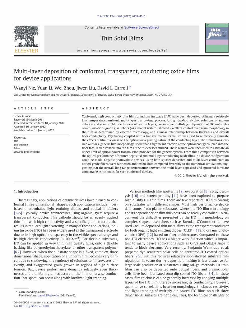
Comparing the single layer ITO quality produced by the three solu-tions as described in Fig. 1, the best film was observed from the useof the 6 wt.% of In2O3 solution mixed with InCl3 and SnCl4·5H2O inalcohol. Generally speaking, the 6 wt.% solutions produced a slightlythinner single layer, than the higher concentration films (40 nm com-pared to 60 nm for the 20 wt.%). Furthermore, the films appear con-tinuous and smooth for this concentration. Naturally, it is expectedthat this will depend on the withdrawal rates and temperature of
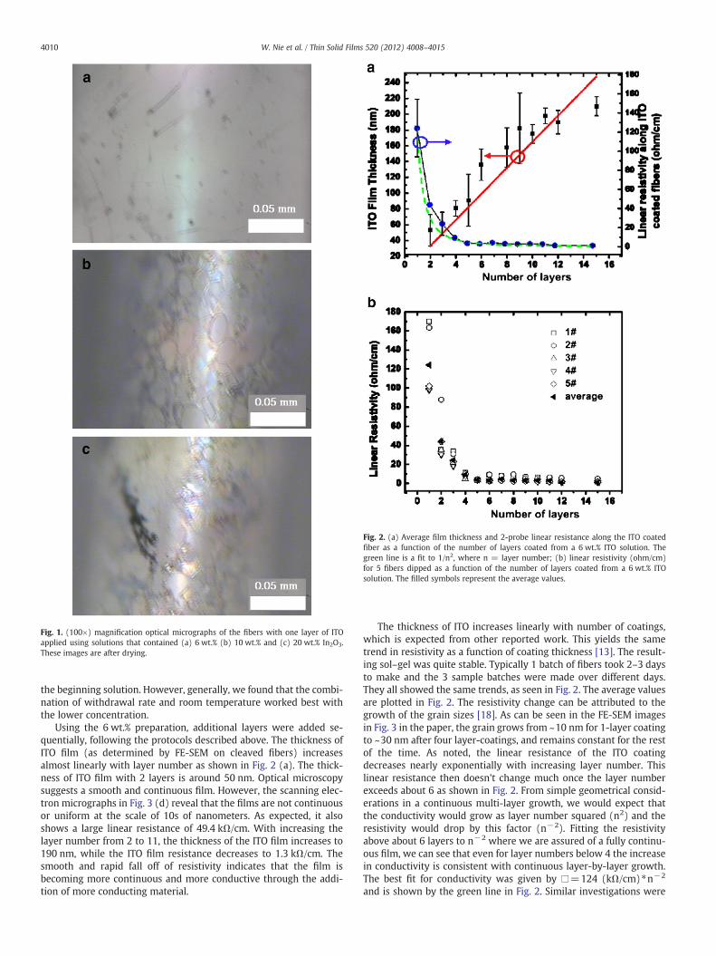
Fig. 1. (100×) magnification optical micrographs of the fibers with one layer of ITOapplied using solutions that contained (a) 6 wt.% (b) 10 wt.% and (c) 20 wt.% In2O3.These images are after drying.
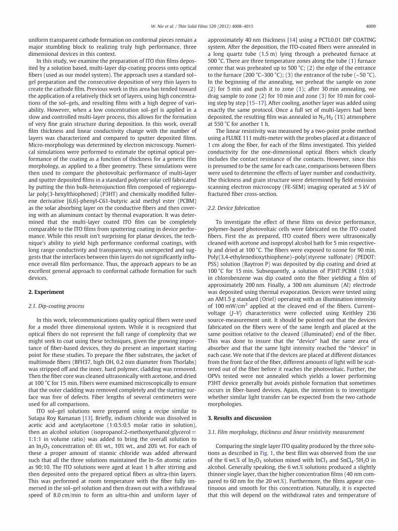
Fig. 2. (a) Average film thickness and 2-probe linear resistance along the ITO coatedfiber as a function of the number of layers coated from a 6 wt.% ITO solution. Thegreen line is a fit to 1/n2, where n = layer number; (b) linear resistivity (ohm/cm)for 5 fibers dipped as a function of the number of layers coated from a 6 wt.% ITOsolution. The filled symbols represent the average values.
4010 W. Nie et al. / Thin Solid Films 520 (2012) 4008–4015
the beginning solution. However, generally, we found that the combi-nation of withdrawal rate and room temperature worked best withthe lower concentration.
Using the 6 wt.% preparation, additional layers were added se-quentially, following the protocols described above. The thickness ofITO film (as determined by FE-SEM on cleaved fibers) increasesalmost linearly with layer number as shown in Fig. 2 (a). The thick-ness of ITO film with 2 layers is around 50 nm. Optical microscopysuggests a smooth and continuous film. However, the scanning elec-tron micrographs in Fig. 3 (d) reveal that the films are not continuousor uniform at the scale of 10s of nanometers. As expected, it alsoshows a large linear resistance of 49.4 kΩ/cm. With increasing thelayer number from 2 to 11, the thickness of the ITO film increases to190 nm, while the ITO film resistance decreases to 1.3 kΩ/cm. Thesmooth and rapid fall off of resistivity indicates that the film isbecoming more continuous and more conductive through the addi-tion of more conducting material.
The thickness of ITO increases linearly with number of coatings,which is expected from other reported work. This yields the sametrend in resistivity as a function of coating thickness [13]. The result-ing sol–gel was quite stable. Typically 1 batch of fibers took 2–3 daysto make and the 3 sample batches were made over different days.They all showed the same trends, as seen in Fig. 2. The average valuesare plotted in Fig. 2. The resistivity change can be attributed to thegrowth of the grain sizes [18]. As can be seen in the FE-SEM imagesin Fig. 3 in the paper, the grain grows from ~10 nm for 1-layer coatingto ~30 nm after four layer-coatings, and remains constant for the restof the time. As noted, the linear resistance of the ITO coatingdecreases nearly exponentially with increasing layer number. Thislinear resistance then doesn't change much once the layer numberexceeds about 6 as shown in Fig. 2. From simple geometrical consid-erations in a continuous multi-layer growth, we would expect thatthe conductivity would grow as layer number squared (n2) and theresistivity would drop by this factor (n−2). Fitting the resistivityabove about 6 layers to n−2 where we are assured of a fully continu-ous film, we can see that even for layer numbers below 4 the increasein conductivity is consistent with continuous layer-by-layer growth.The best fit for conductivity was given by □=124 (kΩ/cm)⁎n−2
and is shown by the green line in Fig. 2. Similar investigations were
4011W. Nie et al. / Thin Solid Films 520 (2012) 4008–4015
carried out on the other concentrations and on larger diameter fiberswith similar results (not shown here). In comparison a sputter coated,single monolith ITO coating has a linear resistivity of 1.1 kΩ/cm at athickness of 200 nm.
With increasing layer number, increasing smoothness and welldefined grain structure is observed as shown in Fig. 3. With 11 con-secutive layers, the ITO film is generally very uniform and smootharound the fiber surface. Fig. 3 (b) shows a FE-SEM image of thecross section of an ITO eleven-layered fiber. The thickness of the ITOfilm is around 190 nm and compares nicely to that of a sputtered200 nm film as shown in Fig. 3 (a). The overall grain size for theeleven-layer film is approximately 30 nm, similar to that of the sput-tered film. A reasonable range of 20–50 nm ITO thickness in planarfilms has been reported using sol–gel methods [19,20]. Fig. 2 (c)–(h)shows the evolution of the film as the layer number is increased.Notice that the ITO grains aggregate/grow from ~10 nm in the mono-layer ITO to ~30 nm after four layers. Of course, the grain size is esti-mated in these micrographs from the overall diameter along thesurface. We do note that the sputtered film grains exhibit a morecolumnar grain growth than that of the multi-layer film which hasmore rounded grain and with grains stacked one on another toachieve the overall thickness observed. This difference in morphologymay explain the slight differences in 2-probe conductivity observedbetween the sputter coated and multi-layer films. It is also importantto state that variations in stoichiometry can result in significantchanges in the conductivity of such films [21]. To address this, boththe multi-layer and sputter deposition coatings were post-treated insimilar ways. Though this doesn't guarantee exactly the same stoichi-ometry between the films, we postulate that the overall stoichiometry
Fig. 3. (a) FE-SEM of ITO film on 0.2 mm fiber after sputter coating; FE-SEM of ITO film on 0layers and (h) 15 layers of the ITO solution. Fibers were prepared for imaging by fracturing an5 kV. (The top, outer layer, of the fiber is marked in each micrograph).
of the grains is similar and the grain morphology is the primary driverbetween conductivity differences. Further experiments are planned toconfirm this.
The optical transparency determination is hard to carry out evenfor a planer substrate due to the thickness dependence of each cycleof dip-coating as shown in Eq. (3.1) [22]:
h∝ffiffiffiffiffiffiffiffiffiffiffiffiffiffiffiffiffiffiγρg
Ca1
2=
rð3:1Þ
h thicknessγ surface tensionρg gravityCa capillary number.
Therefore, the single layer dip-coating thickness not only dependson the viscosity of solution and velocity of withdrawing speed, butalso relates with the surface tension which is a function of dimension/curvature of the object. So a flat substrate may not be able toreproduce the same characteristic film on optical fibers as was ourworry.
3.2. Organic photovoltaic device performance on indium tin oxidedip-coated fibers
Performance in a photonic or opto-electronic application dependsnot only on the electrical conductivity of the films but also on itsoptical properties such as transparency and scattering. It is naturalto assume that the differences in granularity may lead to quite
.2 mm fiber with (b) 11 layers, (c) 1 layer, (d) 2 layers, (e) 4 layers, (f) 5 layers, (g) 7d adding a thin layer of Au to reduce charging of the glass. The FE-SEMwas operated at
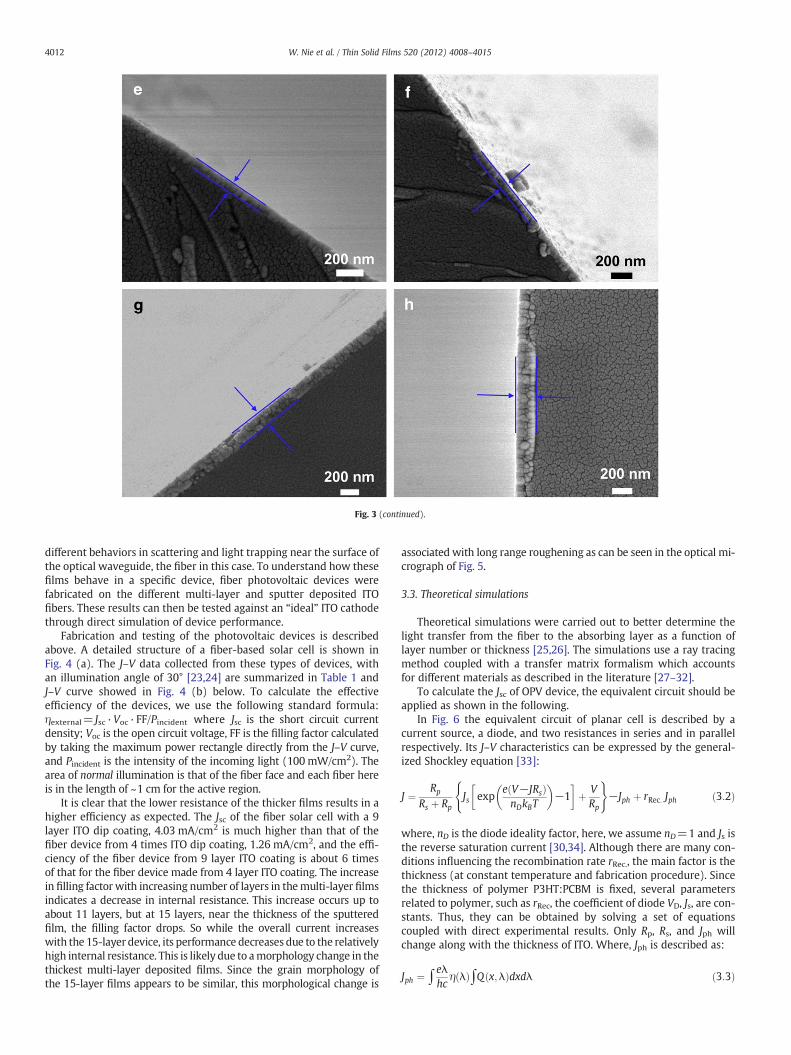
Fig. 3 (continued).
4012 W. Nie et al. / Thin Solid Films 520 (2012) 4008–4015
different behaviors in scattering and light trapping near the surface ofthe optical waveguide, the fiber in this case. To understand how thesefilms behave in a specific device, fiber photovoltaic devices werefabricated on the different multi-layer and sputter deposited ITOfibers. These results can then be tested against an “ideal” ITO cathodethrough direct simulation of device performance.
Fabrication and testing of the photovoltaic devices is describedabove. A detailed structure of a fiber-based solar cell is shown inFig. 4 (a). The J–V data collected from these types of devices, withan illumination angle of 30° [23,24] are summarized in Table 1 andJ–V curve showed in Fig. 4 (b) below. To calculate the effectiveefficiency of the devices, we use the following standard formula:ηexternal= Jsc ·Voc ·FF/Pincident where Jsc is the short circuit currentdensity; Voc is the open circuit voltage, FF is the filling factor calculatedby taking the maximum power rectangle directly from the J–V curve,and Pincident is the intensity of the incoming light (100 mW/cm2). Thearea of normal illumination is that of the fiber face and each fiber hereis in the length of ~1 cm for the active region.
It is clear that the lower resistance of the thicker films results in ahigher efficiency as expected. The Jsc of the fiber solar cell with a 9layer ITO dip coating, 4.03 mA/cm2 is much higher than that of thefiber device from 4 times ITO dip coating, 1.26 mA/cm2, and the effi-ciency of the fiber device from 9 layer ITO coating is about 6 timesof that for the fiber device made from 4 layer ITO coating. The increasein filling factor with increasing number of layers in themulti-layer filmsindicates a decrease in internal resistance. This increase occurs up toabout 11 layers, but at 15 layers, near the thickness of the sputteredfilm, the filling factor drops. So while the overall current increaseswith the 15-layer device, its performance decreases due to the relativelyhigh internal resistance. This is likely due to amorphology change in thethickest multi-layer deposited films. Since the grain morphology ofthe 15-layer films appears to be similar, this morphological change is
associated with long range roughening as can be seen in the optical mi-crograph of Fig. 5.
3.3. Theoretical simulations
Theoretical simulations were carried out to better determine thelight transfer from the fiber to the absorbing layer as a function oflayer number or thickness [25,26]. The simulations use a ray tracingmethod coupled with a transfer matrix formalism which accountsfor different materials as described in the literature [27–32].
To calculate the Jsc of OPV device, the equivalent circuit should beapplied as shown in the following.
In Fig. 6 the equivalent circuit of planar cell is described by acurrent source, a diode, and two resistances in series and in parallelrespectively. Its J–V characteristics can be expressed by the general-ized Shockley equation [33]:
J ¼ Rp
Rs þ RpJs exp
e V−JRsð ÞnDkBT
� �−1
� �þ VRp
( )−Jph þ rRec: Jph ð3:2Þ
where, nD is the diode ideality factor, here, we assume nD=1 and Js isthe reverse saturation current [30,34]. Although there are many con-ditions influencing the recombination rate rRec., the main factor is thethickness (at constant temperature and fabrication procedure). Sincethe thickness of polymer P3HT:PCBM is fixed, several parametersrelated to polymer, such as rRec, the coefficient of diode VD, Js, are con-stants. Thus, they can be obtained by solving a set of equationscoupled with direct experimental results. Only Rp, Rs, and Jph willchange along with the thickness of ITO. Where, Jph is described as:
Jph ¼ ∫ eλhc
η λð Þ∫Q x;λð Þdxdλ ð3:3Þ
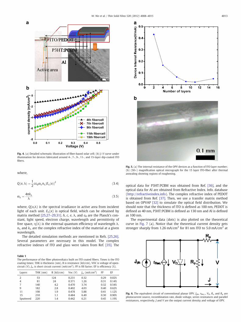
Fig. 5. (a) The internal resistance of the OPV devices as a function of ITO layer number;(b) (50×) magnification optical micrograph for the 15 layer ITO-fiber after thermalannealing showing regions of roughening.
Fig. 4. (a) Detailed schematic illustration of fiber-based solar cell; (b) J–V curve underillumination for devices fabricated around 4-, 7-, 9-, 11-, and 15-layer dip-coated ITOfibers.
4013W. Nie et al. / Thin Solid Films 520 (2012) 4008–4015
where,
Q x;λð Þ ¼ 12cε0αλnλ Eλ xð Þj j2 ð3:4Þ
αλ ¼ 4πkλλ
ð3:5Þ
where, Q(x,λ) is the spectral irradiance in active area from incidentlight of each unit. Eλ(x) is optical field, which can be obtained bymatrix method [25,27–29,31]. h, c, e, λ, and ε0 are the Planck's con-stant, light speed, electron charge, wavelength and permittivity offree space, η(λ) is the external quantum efficiency of wavelength λ.nλ and kλ are the complex refractive index of the material at a givenwavelength.
The detailed simulation methods are mentioned in Refs. [25,26].Several parameters are necessary in this model. The complexrefractive indexes of ITO and glass were taken from Ref. [35]. The
Table 1The performance of the fiber photovoltaics built on ITO coated fibers. Times is the ITOcoating times; THK is thickness (nm), R is resistance (kΩ/cm), VOC is voltage of open-circuit (V); Jsc is short circuit current (mA/cm2); FF is fill factor; EF is efficiency (%).
Layers THK (nm) R (kΩ/cm) Voc (V) Jsc (mA/cm2) FF EF
2 53 124 0.231 0.32 0.29 0.02%4 81 24 0.371 1.26 0.31 0.14%7 140 4.2 0.470 3.74 0.32 0.54%9 182 2.8 0.402 4.03 0.40 0.62%11 198 1.9 0.478 5.88 0.41 1.12%15 210 1.1 0.484 6.49 0.30 0.90%Sputtered 220 1.4 0.442 6.21 0.45 1.19%
optical data for P3HT:PCBM was obtained from Ref. [36], and theoptical data for Al are obtained from Refractive Index. Info. database(http://refractiveindex.info). The complex refractive index of PEDOTis obtained from Ref. [37]. Then, we use a transfer matrix methodbased on OPVAP [32] to simulate the optical field distribution. Weshould note that the thickness of ITO is defined as 100 nm, PEDOT isdefined as 40 nm, P3HT:PCBM is defined as 130 nm and Al is definedas 100 nm.
The experimental data (dots) is also plotted on the theoreticalcurve in Fig. 7 (a). Notice that the theoretical current density getsstronger sharply from 1.26 mA/cm2 for 81 nm ITO to 5.0 mA/cm2 at
Fig. 6. The equivalent circuit of conventional planar OPV. Jph, rRec.., VD, Rs, and Rp arephotocurrent source, recombination rate, diode voltage, series resistances and parallelresistances, respectively. J and V are the output current density and voltage of OPV.
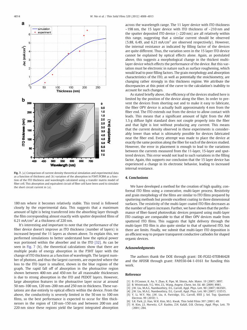
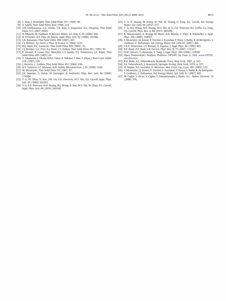
Fig. 7. (a) Comparison of current density theoretical simulation and experimental dataas a function of thickness and (b) variation of the absorption in P3HT:PCBM as a func-tion of the ITO thickness and wavelength calculated using a transfer matrix model offiber cell. This absorption and equivalent circuit of fiber cell have been used to simulatethe short circuit current in (a).
4014 W. Nie et al. / Thin Solid Films 520 (2012) 4008–4015
180 nm where it becomes relatively stable. This trend is followedclosely by the experimental data. This suggests that a maximumamount of light is being transferred into the absorbing layer throughthe film corresponding almost exactly with sputter deposited films of6.21 mA/cm2 at a thickness of 220 nm.
It's interesting and important to note that the performance of thefiber device doesn't improve as ITO thickness (number of layers) isincreased beyond the 11 layers as shown above. To explain this, weperformed simulations to better understand how the optical powerwas portioned within the absorber and in the ITO [32]. As can beseen in Fig. 7 (b), the theoretical calculations show that there aremultiple peaks of energy absorption in the P3HT layer with thechange of ITO thickness as a function of wavelength. The largest num-ber of photons, and thus the largest currents, are expected where theloss to the ITO layer is smallest, shown in the blue regions of thegraph. The rapid fall off of absorption in the photoactive regionshown between 400 nm and 450 nm for all reasonable thicknessesis due to strong absorption in the ITO and PEDOT layers. However,large absorption features in the photoactive layer occur at around50 nm–100 nm, 120 nm–200 nm and 250 nm in thickness. These var-iations are due entirely to optical effects within the device. From theabove, the conductivity is severely limited in the 50 nm to 100 nmfilms, so the best performance is expected to occur for film thick-nesses in the region of 120 nm–150 nm and between 200 nm and220 nm since these regions yield the largest integrated absorption
across the wavelength range. The 11 layer device with ITO thickness~198 nm, the 15 layer device with ITO thickness of ~210 nm andthe sputter deposited ITO device (~220 nm) are all relatively withinthis range, suggesting that a similar current should be observed(5.88, 6.49, and 6.21 mA/cm2 are observed respectively). However,the internal resistance as indicated by filling factor of the devicesare quite different. Thus, the variation seen in the 15 layer ITO devicecannot be explained by optical effects alone. Again, as postulatedabove, this suggests a morphological change in the thickest multi-layer device which effects the performance of the device. But this var-iation must be electronic in nature such as surface roughening, whichwould lead to poor filling factors. The grain morphology and absorptioncharacteristics of the ITO, as well as potentially the stoichiometry, arechanging rather strongly in this thickness regime. We attribute thediscrepancies at this point of the curve to the calculation's inability toaccount for such changes.
As stated briefly above, the efficiency of the devices studied here islimited by the position of the device along the fiber. In order to pre-vent the devices from shorting out and to make it easy to fabricate,the fiber OPV device is actually built approximately 4 mm from thefiber end. The ITO extends out from the device to allow contact withleads. This means that a significant amount of light from the AM1.5 g diffuse light standard does not couple properly into the fiberand that light is lost without producing any current. This meansthat the current density observed in these experiments is consider-ably lower than what is ultimately possible for devices fabricatednear the fiber end. Every attempt was made to place the device atexactly the same position along the fiber for each of the devices studied.However, the error in placement is enough to lead to the variationsbetween the currents measured from the 11-layer, 15-layer and sput-tered devices. This error would not lead to such variations in the fillingfactor. Again, this supports our conclusion that the 15 layer device hasexperienced a change in its electronic behavior, leading to increasedinternal resistance.
4. Conclusions
We have developed a method for the creation of high quality, con-formal ITO films using a consecutive, multi-layer process. Resistivityand grain morphology of the films are similar to ITO films prepared bysputtering methods but provide excellent coating to three dimensionalsurfaces. The resistivity of the multi-layer coated ITO film decreases asthe number of layers increases. Further, we have shown that the perfor-mance of fiber-based photovoltaic devices prepared using multi-layerITO coatings are comparable to that of fiber OPV devices made fromsputtered ITO films. This suggests that light delivery through themulti-layer ITO film is also quite similar to that of sputtered ITO, butthere are limits. Finally, we submit that multi-layer ITO deposition isan efficient way to prepare transparent conductive cathodes for shapedorganic devices.
Acknowledgments
The authors thank the DOE through grant: DE-FG02-07ER46428and the AFOSR through grant: FA9550-04-1-0161 for funding thiswork.
Reference
[1] B. O'Connor, K. An, Y. Zhao, K. Pipe, M. Shtein, Adv. Mater. 19 (2007) 3897.[2] B. Weintraub, Y.G. Wei, Z.L. Wang, Angew. Chem. Int. Ed. 48 (2009) 8981.[3] J.W. Liu, M.A.G. Namboothiry, D.L. Carroll, Appl. Phys. Lett. 90 (2007) 063501.[4] J.W. Liu, M.A.G. Namboothiry, D.L. Carroll, Appl. Phys. Lett. 90 (2007) 133515.[5] Y. Li, W.Y. Nie, J.W. Liu, A. Partridge, D.L. Carroll, IEEE J. Sel. Top. Quantum
Electron. 99 (2010) 1.[6] S.K. Park, J.I. Han, W.K. Kim, M.G. Kwak, Thin Solid Films 397 (2001) 49.[7] H. Kim, J.S. Horwitz, G.P. Kushto, Z.H. Kafafi, D.B. Chrisey, Appl. Phys. Lett. 79
(2001) 284.
4015W. Nie et al. / Thin Solid Films 520 (2012) 4008–4015
[8] C. May, J. Strumpfel, Thin Solid Films 351 (1999) 48.[9] A. Salehi, Thin Solid Films 324 (1998) 214.
[10] A.B. Chebotareva, G.G. Untila, T.N. Kost, S. Jorgensen, A.G. Ulyashin, Thin SolidFilms 515 (2007) 8505.
[11] H. Mbarek, M. Saadoun, B. Bessais, Mater. Sci. Eng., C 26 (2006) 500.[12] B. O'Connor, K.P. Pipe, M. Shtein, Appl. Phys. Lett. 92 (2008) 193306.[13] S.R. Ramanan, Thin Solid Films 389 (2001) 207.[14] C.J. Brinker, A.J. Hurd, J. Phys. III France 4 (1994) 1231.[15] M.J. Alam, D.C. Cameron, Thin Solid Films 420 (2002) 76.[16] C.J. Brinker, G.C. Frye, A.J. Hurd, C.S. Ashley, Thin Solid Films 201 (1991) 97.[17] K. Daoudi, B. Canut, M.G. Blanchin, C.S. Sandu, V.S. Teodorescu, J.A. Roger, Thin
Solid Films 445 (2003) 20.[18] Y. Takahashi, S. Okada, R.B.H. Tahar, K. Nakano, T. Ban, Y. Ohya, J. Non-Cryst. Solids
218 (1997) 129.[19] J. Herrero, C. Guillen, Thin Solid Films 451 (2004) 630.[20] H.Y. Valencia, L.C. Moreno, A.M. Ardila, Microelectron. J. 39 (2008) 1356.[21] M. Mizuhashi, Thin Solid Films 76 (1981) 97.[22] J.H. Snoeijer, G. Delon, M. Fermigier, B. Andreotti, Phys. Rev. Lett. 96 (2006)
174504.[23] Y. Li, W. Zhou, D. Xue, J.W. Liu, E.D. Peterson, W.Y. Nie, D.L. Carroll, Appl. Phys.
Lett. 95 (2009) 203503.[24] Y. Li, E.D. Peterson, H.H. Huang, M.J. Wang, D. Xue, W.Y. Nie, W. Zhou, D.L. Carroll,
Appl. Phys. Lett. 96 (2010) 243505.
[25] Y. Li, H. Huang, M. Wang, W. Nie, W. Huang, G. Fang, D.L. Carroll, Sol. EnergyMater. Sol. Cells 98 (2012) 273.
[26] Y. Li, M.J. Wang, H.H. Huang, W.Y. Nie, Q. Li, E.D. Peterson, R.C. Coffin, G.J. Fang,D.L. Carroll, Phys. Rev. B. 84 (2011) 085206.
[27] R. Hausermann, E. Knapp, M. Moos, N.A. Reinke, T. Flatz, B. Ruhstaller, J. Appl.Phys. 106 (2009) 104507.
[28] F. Monestier, J.J. Simon, P. Torchio, L. Escoubas, F. Flory, S. Bailly, R. de Bettignies, S.Guillerez, C. Defranoux, Sol. Energy Mater. Sol. Cells 91 (2007) 405.
[29] L.A.A. Pettersson, L.S. Roman, O. Inganas, J. Appl. Phys. 86 (1999) 487.[30] B.P. Rand, D.P. Burk, S.R. Forrest, Phys. Rev. B. 75 (2007) 115327.[31] D.W. Sievers, V. Shrotriya, Y. Yang, J. Appl. Phys. 100 (2006) 114509.[32] Open Photovoltaics Analysis Platform (OPVAP) by Yuan Li, USA, www.OPVAP.
inwake.com.[33] R.H. Bube, A.L. Fahrenbruch, Academic Press, New York, 1981, p. 163.[34] A.L. Fahrenbruch, J. Aranovich, Springer-Verlag, New York, 1979, p. 257.[35] H. Hoppe, N.S. Sariciftci, D. Meissner, Mol. Cryst. Liq. Cryst. 385 (2002) 233.[36] F. Monestier, J.J. Simon, P. Torchio, L. Escoubas, F. Florya, S. Bailly, R. de Bettignies,
S. Guillerez, C. Defranoux, Sol. Energy Mater. Sol. Cells 91 (2007) 405.[37] M. Caglar, S. Ilican, Y. Caglar, F. Yakuphanoglu, J. Mater. Sci. - Mater. Electron. 19
(2008) 704.