multi chip module
TRANSCRIPT
MCM
(Multiple-chip-module)

MCM is specialized electronic
package where multiple IC's,
semiconductor dies are packed on to a
unified substrate.
Definition:


They have been introduced as an
alternative packing approach to complement
the advances which were taking place in IC
technology.
Packaging of the chips has become a more
significant factor in performance.
Chip interconnections play a more
dominant & limited role in determining overall
system speed or performance.

PHYSICAL DESIGN AUTOMATION
Physical design is similar as IC’s but designtools were distinct and cannot be directly usedfor MCM.
In designing the CAD tools for MCM followingwere taken in to consideration.
1. Clock skew rate
2. Power noise disturbance
3. Assembly effects

MCM -TYPES
Non-Programmable MCM’s
1. MCM-L (Laminated MCM)
2. MCM-C (Ceramic substrate MCM)
3. MCM-D (Deposited MCM)
For fast turn around we go for PMCM’S.

MCM-L
It is the oldest technology.
It is an advanced PCB which IC aremounted using COB(chip on board)Technology.

It is less cost effective at higher densities wheremany additional layers are required.
It is suitable technology for applications whichrequire low risk packing approach.
ADVANTAGES:
1.Low cost.
2.high density
3.High Performance
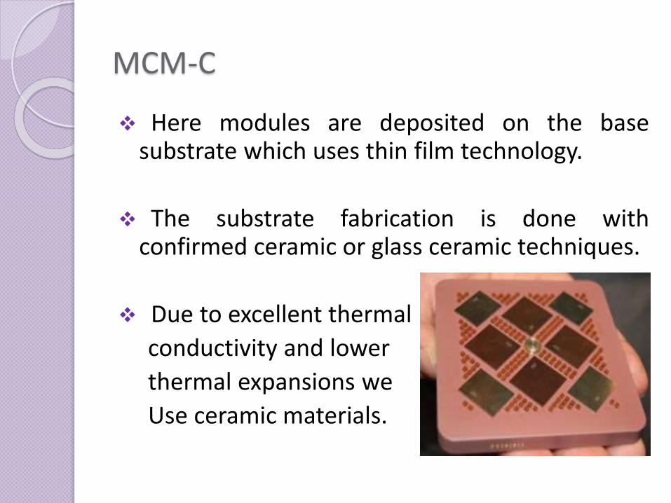
MCM-C
Here modules are deposited on the basesubstrate which uses thin film technology.
The substrate fabrication is done withconfirmed ceramic or glass ceramic techniques.
Due to excellent thermal
conductivity and lower
thermal expansions we
Use ceramic materials.

It is not applicable for high-end applications.
Interconnect densities = 200-400 cm/ cm2.
Advantages:
1.Low cost.
2.High density.
3.High performance.
These have been the primary packing choicein many advanced applications requiring forboth performance & reliability.

MCM-D This consists of substrates which have high
density thin-films metals and low dielectricmaterials like silicon.
Several dielectric/metallization technologieswere involved.
Advantages:
1.High performance.
2.High density.
Disadvantage:
High cost.

COMPARISION

Die Attachment techniques
These attachment techniques are of three types.
1. wire bonding
2. TAB (tape automated bonding)
3. Flip-chip bonding
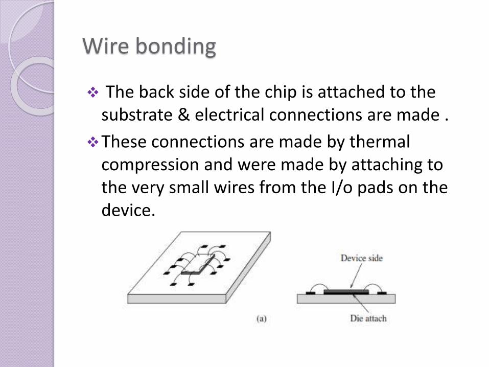
Wire bonding
The back side of the chip is attached to the substrate & electrical connections are made .
These connections are made by thermal compression and were made by attaching to the very small wires from the I/o pads on the device.

TAB
This uses a thin polymer tape containing metallic circuitry.
The actual path is simply a set of connections from inner leads to outer leads.

Flip-chip bonding
This use smaller solder balls on the I/o pads.
These also electrically connected
This also known as Face-down bonding (or) controlled-collapsed chip connection.

MCM Physical design cycle
MCM input = circuit design
MCM output = layout design.
Physical design cycle :
1. Partioning
2.Placement
3.Routing

Partioning
The 1st assignment of partion is to sub-divide the given circuit.
Timing, i/o pin count & power constraints .
As a result area also will also be added as one of the constraints.
It is performance driven.
note: No. of chips sustain in sub-ckt must be less than No. of chips
sustain in MCM.

Placement
Mapping of chips.
It is performance driven.
As a result effects thermal characteristics. Duethis there will be a effect over routing efficiency.
Compared to IC’s they have fewer componentsand sizes, shapes were less variable.
Note: Thermal characteristics were considered because bare chipswere place side by side hence during the processing certainamount of heat is get generated.
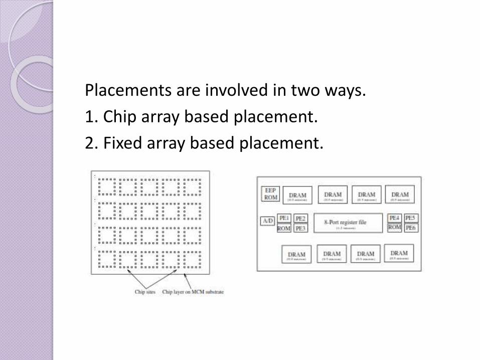
Placements are involved in two ways.
1. Chip array based placement.
2. Fixed array based placement.
