mtle-6120: advanced electronic properties of materials...
TRANSCRIPT

MTLE-6120: Advanced Electronic Properties of Materials
Band theory of solids
Reading:
I Kasap: 4.1 - 4.5
1

Crystals
I Periodic arrangement of atoms (ions: nuclei + core electrons)
I Previously: classical motion of electrons in crystal
I What was the role of the periodicity? None!
I Next: quantum motion of electrons in crystal
I Bravais lattice: regular grid of points
I Lattice vectors ~a1,~a2, ~a3I Any point on grid n1~a1 + n2~a2 + n3 ~a3I Unit cell: repeat at grid points to fill space
I Multiple atoms possible per unit cell
+ + + + +
+ + + + +
+ + + + +
+ + + + +
+
+
+
+
+
+
+
+
+
+
++ + + +
+
+
+
+
+
+
+
+
+
+
+
+
+
+
+
+
+
+
+
+
+ + + + +
+ + + + +
+ + + + +
+ + + + +
2

Classical example: one oscillator
I Mass m attached to a spring with constant k
I Equation of motion in displacement x:
mx = −kx
I In terms of ω0 =√k/m,
x = −ω20x
I Oscillatory solutions e±iω0t with angular frequency ω0
3

Classical example: two oscillators
I Two masses m each attached to a spring with constant k
I Equation of motion in displacements x1 and x2:
mx1 = −kx1mx2 = −kx2
I Solutions: both x1 and x2 oscillate with ω0 =√k/m
4

Classical example: two coupled oscillators
I Two masses m each attached to a spring with constant kI Attached to each other with another spring with constant KI Equation of motion in displacements x1 and x2:
mx1 = −kx1 −K(x1 − x2)
mx2 = −kx2 −K(x2 − x1)
I Coupled equations, x1 and x2 are not each an oscillatorI Add and subtract
m(x1 + x2) = −k(x1 + x2)
m(x1 − x2) = −(k + 2K)(x1 − x2)
I Oscillator differential equations in (x1 ± x2)I (x1 + x2) oscillates with frequency
√k/m
I (x1 − x2) oscillates with frequency√
(k + 2K)/m
5

Coupled oscillators: eigenvalue problem
I Equation of motion in matrix form:
md2
dt2
(x1x2
)= −
(k +K −K−K k +K
)︸ ︷︷ ︸
A
·(x1x2
)
I Coupled equations because of off-diagonal terms in A
I Diagonalize A = V ·D · V −1 using eigenvalue diagonal matrix D andeigenvector diagonal matrix V
md2
dt2V −1 ·
(x1x2
)= −D · V −1 ·
(x1x2
)I V −1 combines x into normal modes x1 + x2 and x1 − x2I Corresponding eigenvalues are mω2 = (k +K)∓K i.e. k and k + 2K
6

Three coupled oscillators
I For three oscillators
A =
k +K −K 0−K k + 2K −K
0 −K k +K
I Eigenvalues mω2: k
k +Kk + 3K
7

N coupled oscillators
I For N oscillators, get N ×N matrix
A =
k +K −K−K k + 2K −K
−K k + 2K. . .
. . .. . . −K−K k + 2K −K
−K k +K
I Consider eigenvector of displacements X = (x1, x2, . . . , xN ) with
eigenvalue mω2 = λ (say)I nth row (n 6= 1, N) of eigenvalue equation AX = λX is
Cxn−1 +Dxn + Cxn+1 = λxn
where C = −K is the coupling (off-diagonal term)and D = k + 2K is the diagonal term
8

Tri-diagonal matrix eigenvalue problemI nth row (n 6= 1, N) of eigenvalue equation AX = λX is
Cxn−1 +Dxn + Cxn+1 = λxn
I Try solution of form xn = eik(na) where a is spacing between oscillators(just so that k has usual dimensions of wavevector)
Ceik(n−1)a +Deikna + Ceik(n+1)a = λeikna
Ce−ika +D + Ceika = λ
D + 2Ccos(ka) = λ
(Each spring has phase eika relative to previous one)I All rows satisfy this condition except first and last
eika(D −K) + Ce2ika = λeika (n = 1)
Cei(N−1)ka + (D −K)eNika = λeNika (n = N)
I Connect last spring to first
9

Periodic boundary conditions (Born-von Karman)I Edge equations after connecting last spring to first
CeNika︸ ︷︷ ︸from n = N
+eikaD + Ce2ika = λeika (n = 1)
Cei(N−1)ka +DeNika + Ceika︸ ︷︷ ︸from n = 1
= λeNika (n = N)
I Canceling common factors:
(eNika)Ce−ika +D + Ceika = λ (n = 1)
Ce−ika +D + Ceika(e−Nika) = λ (n = N)
I These are the same as the other equations when eNika = 1 i.e.k = 2πj/(Na)
I Here, j can be any integer, but for j → j +N , k → k + 2π/a andeika → ei(ka+2π) = eika, so nothing changes
10

N →∞ coupled oscillatorsI Eigenvalues mω2 = λ = D + 2C cos ka = (k + 2K)− 2K cos ka
I k = 2πj/(Na) for j = 0, 1, 2, . . . , N − 1 becomes continuous k ∈ [0, 2π)
I Spacing in k = 2π/(Na) = 2π/L, where L = Na is length of system
k
k+2K
k+4K
-3π/a -2π/a -1π/a 0π/a 1π/a 2π/a 3π/a
k
mω2
I Eigenvalues mω2 form a ‘band’ with range [k, k + 4K]
I Band center set by diagonal element k + 2K
I Band width set by off-diagonal element K (coupling strength)
I Any interval in k of length 2π/a equivalent; conventionally [−π/a, π/a]
11

1D crystal of δ-atomsI An array of δ-potentials at na i.e. V (x) = −V0
∑n δ(x− na)
I Consider E < 0 case first, with κ =√−2mE/~
I Wavefunctions e±κx in each segment, say
ψ(x) = Ane−κ(x−na) +Bne
κ(x−(n+1)a), na < x < (n+ 1)a
12
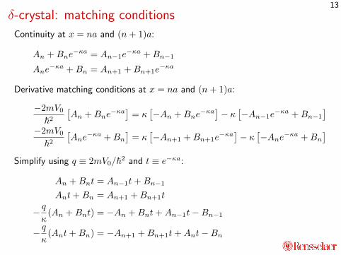
δ-crystal: matching conditions
Continuity at x = na and (n+ 1)a:
An +Bne−κa = An−1e
−κa +Bn−1
Ane−κa +Bn = An+1 +Bn+1e
−κa
Derivative matching conditions at x = na and (n+ 1)a:
−2mV0~2
[An +Bne
−κa] = κ[−An +Bne
−κa]− κ [−An−1e−κa +Bn−1]
−2mV0~2
[Ane
−κa +Bn]
= κ[−An+1 +Bn+1e
−κa]− κ [−Ane−κa +Bn]
Simplify using q ≡ 2mV0/~2 and t ≡ e−κa:
An +Bnt = An−1t+Bn−1
Ant+Bn = An+1 +Bn+1t
− qκ
(An +Bnt) = −An +Bnt+An−1t−Bn−1
− qκ
(Ant+Bn) = −An+1 +Bn+1t+Ant−Bn
13

δ-crystal: eliminate B’sI Add first and third equations, subtract fourth from secondequation:
(1− q/κ)(An +Bnt) = 2An−1t−An +Bnt
(1 + q/κ)(Ant+Bn) = 2An+1 −Ant+Bn
I Collect all A terms to left side and B to right side:
(2− q/κ)An − 2An−1t = (q/κ)Bnt
(2 + q/κ)Ant− 2An+1 = −(q/κ)Bn
I Eliminate Bn:
−An−1t+
(1 + t2 +
(t2 − 1)q
2κ
)An −An+1t = 0
14

δ-crystal: eigenvalue condition
−An−1t+
(1 + t2 +
(t2 − 1)q
2κ
)An −An+1t = 0
I Substitute An = eikna:
−teik(n−1)a +
(1 + t2 +
(t2 − 1)q
2κ
)eikna − teik(n+1)a = 0
−te−ika +
(1 + t2 +
(t2 − 1)q
2κ
)− teika = 0
1 + t2 +(t2 − 1)q
2κ= 2t cos(ka)
1/t+ t
2− q
2κ· 1/t− t
2= cos(ka)
I Since t ≡ e−κa
cosh(κa)− q
2κsinh(κa) = cos(ka)
15

δ-crystal: eigenvaluesI Energy eigenvalue is E = ~ω = −~2κ2
2m
I For the δ-atom, we got a unique κ = mV0/~2 ≡ q/2I But now, an entire family of solutions for k ∈ (−π/a, π/a):
cosh(κa)− q
2κsinh(κa) = cos(ka)
I First consider limit of deep potential i.e. large q; rearrange:
κ =q sinh(κa)
2(cosh(κa)− cos(ka))
I Large q ⇒ large κ⇒ sinh, cosh extremely large
I For q →∞, κ→ q/2 as in the δ-atom
I For large q, substitute κ = q/2 in RHS to get
κ ≈q sinh qa
2
2(cosh qa2 − cos(ka))
≈ q
2
(1 + 2e−qa/2 cos(ka)
)
16

δ-crystal: tight-binding limitI For large q,
κ ≈ q
2
(1 + 2e−qa/2 cos(ka)
)I Correspondingly, the energy
E = −~2κ2
2m≈ −~2q2
8m︸ ︷︷ ︸E0
−~2q2e−qa/2
2mcos(ka)
I Exactly like the coupled springs!
I First term = band center = energy E0 of isolated δ-atom
I Second term ∝ band width and coupling strength ∝ e−qa/2
I Coupling proportional to overlap between wavefunctions at adjacent atoms
17

δ-crystal: free statesI For bound states E = −~2κ2
2m < 0, we derived eigenvalue condition
cosh(κa)− q
2κsinh(κa) = cos(ka)
I For free states E = ~2K2
2m > 0 (using K since k is taken), substituteκ = iK above:
cosh(iKa)− q
2iKsinh(iKa) = cos(ka)
which simplifies to
cos(Ka)− q
2Ksin(Ka) = cos(ka)
18

δ-crystal: energy conditions
cosh(κa)− q
2κsinh(κa) = cos(ka) or cos(Ka)− q
2Ksin(Ka) = cos(ka)
I Plot LHS as a function of E = ~2K2
2m or −~2κ2
2m ; note |RHS| ≤ 1
-1
0
1
-10 -5 0 5 10 15 20 25 30 35 40
For qa = 5cos(ka)
E
h-2/(ma
2)
E = -h-2κ
2/(2m) < 0 E = h-
2K
2/(2m) > 0
I When LHS magnitude > 1, those κ or K not valid solutions
I Correspondingly, not all E valid: bands!
19

δ-crystal: band structureE
h-2/(ma
2)
k
For qa = 5
-20
-10
0
10
20
30
40
-3π/a -2π/a -1π/a 0π/a 1π/a 2π/a 3π/a
I Now plot with respect to k instead
I Repeats when k → k + 2π/a as for the classical springs
20

δ-crystal: band structure qa = 0E
h-2/(ma
2)
k
For qa = 0
-20
-10
0
10
20
30
40
-3π/a -2π/a -1π/a 0π/a 1π/a 2π/a 3π/a
I Potentials no longer present: free electrons!
21

δ-crystal: band structure qa = 1E
h-2/(ma
2)
k
For qa = 1
-20
-10
0
10
20
30
40
-3π/a -2π/a -1π/a 0π/a 1π/a 2π/a 3π/a
I Weak potentials: nearly-free electrons
I Potential opens up ‘gaps’ at k = 0,±π/a
22

δ-crystal: band structure qa = 2E
h-2/(ma
2)
k
For qa = 2
-20
-10
0
10
20
30
40
-3π/a -2π/a -1π/a 0π/a 1π/a 2π/a 3π/a
I Gaps widen as potential gets stronger
I Electrons more tightly bound
23

δ-crystal: band structure qa = 5E
h-2/(ma
2)
k
For qa = 5
-20
-10
0
10
20
30
40
-3π/a -2π/a -1π/a 0π/a 1π/a 2π/a 3π/a
I Band widths reduce as potential gets stronger
I Band structure resembles tight-binding case (C +D cos ka)
24

δ-crystal: band structure qa = 10E
h-2/(ma
2)
k
For qa = 10
-20
-10
0
10
20
30
40
-3π/a -2π/a -1π/a 0π/a 1π/a 2π/a 3π/a
I Bands begin to approach discrete energy levels like atoms
I At same strength, higher energies less affected ⇒ wider bands
25
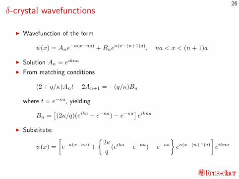
δ-crystal wavefunctions
I Wavefunction of the form
ψ(x) = Ane−κ(x−na) +Bne
κ(x−(n+1)a), na < x < (n+ 1)a
I Solution An = eikna
I From matching conditions
(2 + q/κ)Ant− 2An+1 = −(q/κ)Bn
where t = e−κa, yielding
Bn =[(2κ/q)(eika − e−κa)− e−κa
]eikna
I Substitute:
ψ(x) =
[e−κ(x−na) +
{2κ
q(eika − e−κa)− e−κa
}eκ(x−(n+1)a)
]eikna
26

δ-crystal wavefunctions: Bloch’s theorem
I Same form for E > 0 with κ→ iK, so all wavefunctions of form
ψ(x) =
[e−κ(x−na) +
{2κ
q(eika − e−κa)− e−κa
}eκ(x−(n+1)a)
]eikna
ψ(x) =
[e−iK(x−na) +
{2iK
q(eika − e−iKa)− e−iKa
}eiK(x−(n+1)a)
]eikna
I Relative to start of interval x = na, piece in [ ] identical for each n
I Change from one unit cell to another only in eikna i.e. relative phase eika
I Bloch’s theorem: eigenfunctions of any periodic potential ei~k·~r× periodic
function u~k(~r)
I In this case, periodic part (called Bloch function) is
uk(x) = e−(κ+ik)(x−na)+
[2κ
q(1− e−(κ+ik)a)− e−(κ+ik)a
]e(κ−ik)(x−(n+1)a)
(and similarly for κ→ iK)
27

δ-crystal wavefunctions: tight-binding limit
ψ(x) =
[e−κ(x−na) +
{2κ
q(eika − e−κa)− e−κa
}eκ(x−(n+1)a)
]eikna
I Assume large enough V0 and hence q and κ that e−κa � 1. Also, in thislimit, κ ≈ q/2, so:
ψ(x) ≈ e−κ(x−na)eikna + eκ(x−(n+1)a)eik(n+1)a
I Same form to the left and right of each na, only with κ↔ −κ⇒
ψ(x) ≈∑n
e−κ|x−na|eikna (all x)
I Exactly the δ-atom wavefunction at each na, combined with phase eikna
(analogous to the spring oscillations)
28

δ-crystal wavefunctions: nearly-free limit
I Consider from a different perspective
I Free electron eiKx incident on atom at x = 0
I Reflected wave Re−iKx
I Free electron eiKx incident on atom at x = a
I Reflected wave eiKaRe−iK(x−a) = Re−iKx · e2iKa
I Neighbouring atoms reflect with relative phase e2ika
I Strong reflections at 2Ka = 2nπ ⇒ K = nπ/a
29

δ-crystal: band structure qa = 1E
h-2/(ma
2)
k
For qa = 1
-20
-10
0
10
20
30
40
-3π/a -2π/a -1π/a 0π/a 1π/a 2π/a 3π/a
I Hence strongest effect of potential at K = nπ/a (which is k = 0,±π/a)
I Therefore, potential opens up ‘gaps’ at k = 0,±π/a
30

δ-crystal wavefunctions: general example 1E
h-2/(ma
2)
k
-20
-10
0
10
20
30
40
-1π/a 0π/a 1π/a
For qa = 5Re Ψ(x)
0a 1a 2a 3a 4a 5a
I Bound state with k ≈ 0
I Similar phase at x = na
31

δ-crystal wavefunctions: general example 2E
h-2/(ma
2)
k
-20
-10
0
10
20
30
40
-1π/a 0π/a 1π/a
For qa = 5Re Ψ(x)
0a 1a 2a 3a 4a 5a
I Bound state with k ≈ π/(2a)
I Phase at x = na has period ∼ 4 unit cells
32

δ-crystal wavefunctions: general example 3E
h-2/(ma
2)
k
-20
-10
0
10
20
30
40
-1π/a 0π/a 1π/a
For qa = 5Re Ψ(x)
0a 1a 2a 3a 4a 5a
I Bound state with k ≈ π/aI Phase at x = na has period ∼ 2 unit cells (alternates sign)
I Maximum probability at attractive δ-potential: lower energy
33

δ-crystal wavefunctions: general example 4E
h-2/(ma
2)
k
-20
-10
0
10
20
30
40
-1π/a 0π/a 1π/a
For qa = 5Re Ψ(x)
0a 1a 2a 3a 4a 5a
I Free state with k ≈ π/aI Phase at x = na has period ∼ 2 unit cells (alternates sign)
I Minimum probability at attractive δ-potential: higher energy
I Jump between this and previous case causes jump in energy ⇒ band gap
34

δ-crystal wavefunctions: general example 5E
h-2/(ma
2)
k
-20
-10
0
10
20
30
40
-1π/a 0π/a 1π/a
For qa = 5Re Ψ(x)
0a 1a 2a 3a 4a 5a
I Free state with k ≈ π/(2a)
I Phase at x = na has period ∼ 4 unit cells
35

δ-crystal wavefunctions: general example 6E
h-2/(ma
2)
k
-20
-10
0
10
20
30
40
-1π/a 0π/a 1π/a
For qa = 5Re Ψ(x)
0a 1a 2a 3a 4a 5a
I Free state with k ≈ 0
I Similar phase at x = na
36

δ-crystal wavefunctions: general example 7E
h-2/(ma
2)
k
-20
-10
0
10
20
30
40
-1π/a 0π/a 1π/a
For qa = 5Re Ψ(x)
0a 1a 2a 3a 4a 5a
I Free state with k ≈ 0, but higher K
I Similar phase at x = na, but more oscillations within each unit cell
37

δ-crystal wavefunctions: general example 8E
h-2/(ma
2)
k
-20
-10
0
10
20
30
40
-1π/a 0π/a 1π/a
For qa = 5Re Ψ(x)
0a 1a 2a 3a 4a 5a
I Free state with k ≈ π/(2a)
I Phase at x = na has period ∼ 4 unit cells
38

δ-crystal wavefunctions: general example 9E
h-2/(ma
2)
k
-20
-10
0
10
20
30
40
-1π/a 0π/a 1π/a
For qa = 5Re Ψ(x)
0a 1a 2a 3a 4a 5a
I Free state with k ≈ π/aI Phase at x = na has period ∼ 2 unit cells (alternates sign)
39

Many electrons
I So far: energy of a single electron in a periodic potential
I Reality: many interacting electrons
I DFT picture: eigen-states of effective potential VKS(~r), fill up electrons inascending order of energy
I Assume δ-crystal potential was such an effective potential
I To fill electrons, need to know how many states in a band?
I Periodic boundary conditions in length L, spacing in k is 2π/L
I Range of k is from −π/a to +π/a with length 2π/a
I Therefore, number of k is (2π/a)/(2π/L) = L/a = number of unit cells
I So one electron per unit cell ⇔ one set of ~k ∈ [−π/a, π/a]
I Except spin! Two electrons per unit cell ⇔ one set of ~k ∈ [−π/a, π/a]
40

Filling up electrons
k
Eh-2/(ma2)
0
10
20
30
40
-π/a 0 π/a
1/cell2/cell
3/cell
4/cell
5/cell
6/cell
I Filled state with maximum energy:Highest Occupied Molecular Orbital(HOMO)
I Empty state with minimum energy:Lowest Unoccupied Molecular Orbital(LUMO)
I Each electron/cell fills half a band
I Odd electrons/cell: HOMO = LUMOin middle of band ⇒ metal
I Even electrons/cell: HOMO at bandmaximum, gap to LUMO at nextband minimum ⇒ semiconductor /insulator
I Two types of semiconductors in 1D:direct gap at Γ i.e. k = 0 ordirect gap at zone boundary k = ±π
a
41

Beyond one dimension
I So far: 1D crystal, unit cell length a
I Electron energies depend on Bloch wave-vector k periodic with 2π/a
I Periodicity because phase between unit cells eika unchanged whenk → k + 2π/a
I Therefore we could represent all properties in interval [−π/a, π/a]
I In 3D, crystal represented by lattice vectors ~a1, ~a2 and ~a3I Electron energies depend on Bloch wave-vector ~k
I What is the periodicity in ~k?
I Phase between unit cells ei~k·~aj along jth lattice direction (j = 1, 2, 3)
I If ~k → ~k + ~G such that ~G · ~aj = 2πnj , then
ei~k·~aj → ei(
~k+~G)·~aj = ei~k·~ajei2πnj = ei
~k·~aj (unchanged)
42

Reciprocal lattice
I Consider vectors ~bi defined such that ~bi · ~aj = 2πδij
I Suppose ~G =∑imi
~bi ≡ m1~b1 +m2
~b2 +m3~b3 with mi integers
I Then ~G · ~aj =∑imi
~bi · ~aj =∑imiδij = mj (an integer)
I So all the ~G that leave ei~k·~aj unchanged also a lattice with basis vectors
~b1, ~b2, ~b3I Let A = (~a1,~a2,~a3) and B = (~b1,~b2,~b3)
(3x3 matrices with vectors in columns)
I Defining condition written as BT ·A = 2πI ⇒ B = 2πA−T
(generalization of 2π/a)
I Specifically in 3D, this inverse can be written explicitly as
~b1 =2π(~a2 × ~a3)
~a1 · (~a2 × ~a3), ~b2 =
2π(~a3 × ~a1)
~a2 · (~a3 × ~a1), and ~b3 =
2π(~a1 × ~a2)
~a3 · (~a1 × ~a2)
I Reciprocal lattice vectors relevant for (X-ray / electron) diffraction from
crystals because constructive interference when ei~G·~aj = 1
43

Brillouin zone
I Unit cell of the reciprocal lattice (any shape possible, only volume matters)
I Fundamental Brillouin zone: set of ~k closer to ~G = 0 than any other~G =
∑imi
~biI In 1D, reduces to [−π/a,+π/a] (i.e. the set of k such that |k| < π/a
I For cubic crystals with spacing a, a cube with |kx|, |ky|, |kz| ≤ π/aI For general lattice, shapes can be quite complex (up to 6 edges in 2D, 14
facets in 3D)
44

Example: FCC latticeI Face centered cubic lattice with cubic length a:
(~a1,~a2,~a3) =a
2
0 1 11 0 11 1 0
I Reciprocal lattice is body-centered with cubic length 4π/a:
(~b1,~b2,~b3) =4π/a
2
−1 1 11 −1 11 1 −1
I Brillouin zone is a truncated octahedron
I 8 hexagonal faces: nearest neighbours
I 6 square faces: next-nearest neighbours
L
W
Γ
K
X
45

Band structure of gold (FCC metal)
I Band structure E(~k) for ~k ∈BZ: need 4D plot!
I Paths connecting special high-symmetry points show important features
-6
-4
-2
0
2
4
6
Γ X W L Γ K
Ener
gy [e
V]
PBEsol+UGLLBscQSGW
Expt
(DFT vs. ARPES [Nature Comm. 5, 5788 (2014)])
I Note complexity compared to 1D:many bands overlapping in energy
I E = 0 typically set to HOMO level
I Valence electrons/cell = 11 (odd), configuration: 5d106s1
L
W
Γ
K
X
46
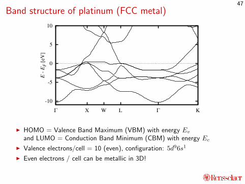
Band structure of platinum (FCC metal)
-10
-5
0
5
10
Γ X W L Γ K
E -
EF [
eV
]
I HOMO = Valence Band Maximum (VBM) with energy Evand LUMO = Conduction Band Minimum (CBM) with energy Ec
I Valence electrons/cell = 10 (even), configuration: 5d96s1
I Even electrons / cell can be metallic in 3D!
47
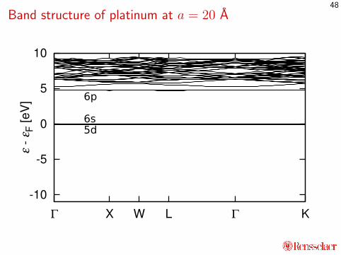
Band structure of platinum at a = 20 A
5d6s
6p
48

Band structure of platinum at a = 10 A
-10
-5
0
5
10
Γ X W L Γ K
ε -
εF [eV
]
49

Band structure of platinum at a = 6 A
-10
-5
0
5
10
Γ X W L Γ K
ε -
εF [eV
]
50

Band structure of platinum at a = 3.92 A
-10
-5
0
5
10
Γ X W L Γ K
ε -
εF [eV
]
51
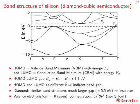
Band structure of silicon (diamond-cubic semiconductor)
E in e
V
6
0
−12L Λ Γ Δ Χ Σ Γ
EvEc
−6
I HOMO = Valence Band Maximum (VBM) with energy Evand LUMO = Conduction Band Minimum (CBM) with energy Ec
I HOMO-LUMO gap Eg = Ec − Ev ≈ 1.1 eV
I HOMO and LUMO at different ~k ⇒ indirect band gap
I Diamond: similar band structure, much larger gap (≈ 5.5 eV) ⇒ insulator
I Valence electrons/cell = 8 (even), configuration: 3s23p2 (two Si/cell)
52

Band structure of GaAs (zinc-blende semiconductor)
I HOMO-LUMO gap Eg = Ec − Ev ≈ 1.4 eV
I HOMO and LUMO at same ~k (Γ) ⇒ direct band gap
I Valence electrons/cell = 8 (even), configuration: Ga(4s24p1), As(4s24p3)
53
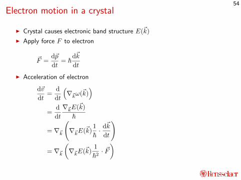
Electron motion in a crystal
I Crystal causes electronic band structure E(~k)
I Apply force F to electron
~F =d~p
dt= ~
d~k
dt
I Acceleration of electron
d~v
dt=
d
dt
(∇~kω(~k)
)=
d
dt
∇~kE(~k)
~
= ∇~k
(∇~kE(~k)
1
~· d~k
dt
)
= ∇~k
(∇~kE(~k)
1
~2· ~F)
54

Effective mass
I Quantum mechanically d~vdt = ∇~k
(∇~kE(~k)/~2 · ~F
)I Compare with classical d~v/dt = ~F/m
I ∇~k(∇~kE(~k)/~2·
)effectively like inverse mass
I In general, effective mass tensor m∗ij(~k) = ~2inv
(∂ki∂kjE(~k)
)I Depends on band and ~k in general, not a single constant!
I For metals, typically report average m∗ for all HOMO levels (Fermi surface)
I For semiconductors, typically report average m∗ each for VBM and CBM
55
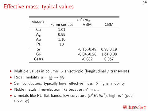
Effective mass: typical values
Materialm∗/me
Fermi surface VBM CBMCu 1.01Ag 0.99Au 1.10Pt 13Si -0.16,-0.49 0.98,0.19Ge -0.04,-0.28 1.64,0.08
GaAs -0.082 0.067
I Multiple values in column ⇒ anisotropic (longitudinal / transverse)
I Recall mobility µ = eτm →
eτm∗
I Semiconductors: typically lower effective mass ⇒ higher mobility
I Noble metals: free-electron like because m∗ ≈ me
I d-metals like Pt: flat bands, low curvature (∂2E/∂k2), high m∗ (poormobility)
56
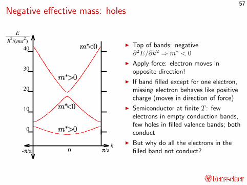
Negative effective mass: holes
k
Eh-2/(ma2)
0
10
20
30
40
-π/a 0 π/a
I Top of bands: negative∂2E/∂k2 ⇒ m∗ < 0
I Apply force: electron moves inopposite direction!
I If band filled except for one electron,missing electron behaves like positivecharge (moves in direction of force)
I Semiconductor at finite T : fewelectrons in empty conduction bands,few holes in filled valence bands; bothconduct
I But why do all the electrons in thefilled band not conduct?
57

Conductivity due to a filled band in 1DI Consider a single filled band E(k) with applied electric field EI Drift velocity of electrons in state k is v(k) = −eEτ/m∗(k)I Average drift velocity of all electrons in band is:
vd = 〈v(k)〉k ≡a
2π
∫ π/a
−π/adkv(k) =
a
2π
∫ π/a
−π/adk (−eEτ/m∗(k))
= −eEτ a2π
∫ π/a
−π/adk
1
m∗(k)= −eEτ a
2π
∫ π/a
−π/adk
∂2E
~2∂k2
= −eEτ a2π
[∂E
~2∂k
]π/a−π/a
= −eEτ a2π
(∂E
~2∂k
∣∣∣∣k=π/a
− ∂E
~2∂k
∣∣∣∣k=−π/a
)= 0
because of the periodicity of E and hence ∂E/∂k.I Filled band does not conduct: positive and negative mass contributions
cancel exactly!I Same proof extends to 3D with some vector calculus
58

Density of statesI Most properties depend on the number of states available at a given energy
I We know distribution of states (per unit volume, including spin) with ~k:∫2dk
2πin 1D,
∫2d~k
(2π)2in 2D,
∫2d~k
(2π)3in 3D
I We used this to count states in frequency intervals for light ω = ck
I In general, given En(~k) for many bands indexed by n, number of states perenergy interval dE:
g(E) =∑n
∫2d~k
(2π)dδ(E − En(~k)) (any dimension)
I For a free electron E(k) = ~2k2/(2m),
g(E) =
(√2m
2π~
)dΘ(E)
2/√E, d = 1
2π, d = 2
4π√E, d = 3
59

Density of states: free electrons
0
5
10
15
0 1 2 3 4 5
g(E
) [e
V-1
nm
-d]
E [eV]
1D2D3D
I Singularity at band edge in 1D (∝ 1/√E)
I Constant and abruptly drops to zero at band edge in 2D
I Goes to zero smoothly at band edge in 3D (∝√E)
60

Density of states: parabolic-band semiconductor
0
1
2
3
4
-3 -2 -1 0 1 2 3 4 5
E [eV]
g(E) [eV-1
nm-3
]Valence band, m
* = -0.3
Conduction band, m* = 0.5
I Parabolic bands near each band edge, with different effective masses
I Overall DOS reduces with reduced effective mass magnitude
61

Density of states: silicon
I Can calculate numerically from band structure
I Parabolic band approximation valid only for narrow energy range near gap
62