mt9v125: soc vga digital image sensor features 1/4-inch ... · † serial lvds data output ......
TRANSCRIPT
MT9V125: SOC VGA Digital Image SensorFeatures
‡
1/4-Inch System-On-A-Chip (SOC) VGANTSC and PAL CMOS Digital Image SensorMT9V125 Datasheet, Rev. WFor the latest datasheet revision, please visit www.onsemi.com
Features• System-on-a-chip (SOC)—completely integrated
camera system• NTSC and PAL (true two field) analog composite
video output• Low power, interlaced scan CMOS image sensor• ITU-R BT.656 parallel output (8-bit, interlaced)• Serial LVDS data output• Supports use of external devices for addition of
custom overlay graphics• Superior low-light performance• On-chip image flow processor (IFP) performs
sophisticated processing• Color recovery and correction, sharpening, gamma,
lens shading correction, and on-the-fly defect correction
• Automatic Features: Auto exposure (AE), auto white balance (AWB), auto black reference (ABR), auto flicker avoidance, auto color saturation, and auto defect identification and correction
• Simple two-wire serial programming interface
Applications• Automotive
– Rear view camera– Side mirror replacement– Blind spot view– Occupant monitoring
• Security cameras• Consumer video products
Data Sheet Applicable To
Silicon Revision: Rev4
MT9V125_DS Rev.. W 6/15 EN 1
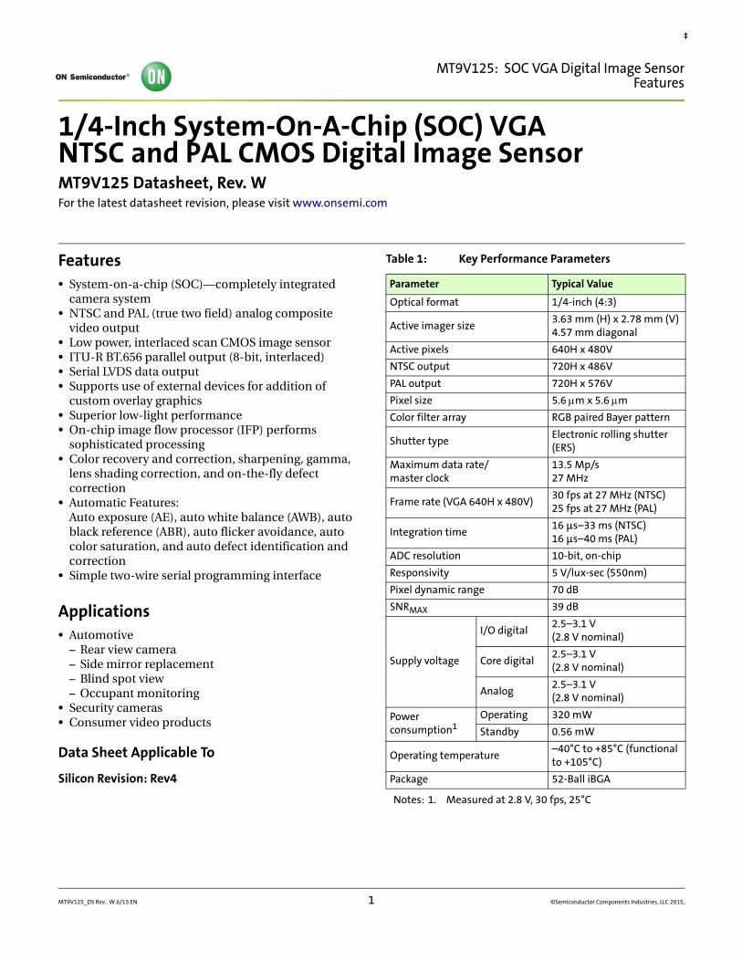
Notes: 1. Measured at 2.8 V, 30 fps, 25°C
Table 1: Key Performance Parameters
Parameter Typical Value
Optical format 1/4-inch (4:3)
Active imager size3.63 mm (H) x 2.78 mm (V)4.57 mm diagonal
Active pixels 640H x 480V
NTSC output 720H x 486V
PAL output 720H x 576V
Pixel size 5.6 m x 5.6 m
Color filter array RGB paired Bayer pattern
Shutter typeElectronic rolling shutter (ERS)
Maximum data rate/master clock
13.5 Mp/s27 MHz
Frame rate (VGA 640H x 480V)30 fps at 27 MHz (NTSC)25 fps at 27 MHz (PAL)
Integration time16 μs–33 ms (NTSC)16 μs–40 ms (PAL)
ADC resolution 10-bit, on-chip
Responsivity 5 V/lux-sec (550nm)
Pixel dynamic range 70 dB
SNRMAX 39 dB
Supply voltage
I/O digital2.5–3.1 V(2.8 V nominal)
Core digital 2.5–3.1 V(2.8 V nominal)
Analog2.5–3.1 V(2.8 V nominal)
Power consumption1
Operating 320 mW
Standby 0.56 mW
Operating temperature–40°C to +85°C (functional to +105°C)
Package 52-Ball iBGA
©Semiconductor Components Industries, LLC 2015,

MT9V125: SOC VGA Digital Image SensorOrdering Information
Ordering Information
See the ON Semiconductor Device Nomenclature document (TND310/D) for a full description of the naming convention used for image sensors. For reference documenta-tion, including information on evaluation kits, please visit our web site at www.onsemi.com.
Table 2: Available Part Numbers
Part Number Product Description Orderable Product Attribute Description
MT9V125IA7XTC-DP Color, 0deg CRA, iBGA Package Drypack, Protective Film
MT9V125IA7XTC-DR Color, 0deg CRA, iBGA Package Drypack
MT9V125IA7XTC-TP Color, 0deg CRA, iBGA Package Tape & Reel, Protective Film
MT9V125IA7XTC-TR Color, 0deg CRA, iBGA Package Tape & Reel
MT9V125_DS Rev.. W 6/15 EN 2 ©Semiconductor Components Industries, LLC,2015.
MT9V125_DS Rev.. W 6/15 EN 3 ©Semiconductor Components Industries, LLC,2015.
MT9V125: SOC VGA Digital Image SensorTable of Contents
Table of Contents
Features . . . . . . . . . . . . . . . . . . . . . . . . . . . . . . . . . . . . . . . . . . . . . . . . . . . . . . . . . . . . . . . . . . . . . . . . . . . . . . . . . . . . . . . . . . . . . .1Applications . . . . . . . . . . . . . . . . . . . . . . . . . . . . . . . . . . . . . . . . . . . . . . . . . . . . . . . . . . . . . . . . . . . . . . . . . . . . . . . . . . . . . . . . . .1Ordering Information. . . . . . . . . . . . . . . . . . . . . . . . . . . . . . . . . . . . . . . . . . . . . . . . . . . . . . . . . . . . . . . . . . . . . . . . . . . . . . . . . .2General Description . . . . . . . . . . . . . . . . . . . . . . . . . . . . . . . . . . . . . . . . . . . . . . . . . . . . . . . . . . . . . . . . . . . . . . . . . . . . . . . . . . .6Functional Overview. . . . . . . . . . . . . . . . . . . . . . . . . . . . . . . . . . . . . . . . . . . . . . . . . . . . . . . . . . . . . . . . . . . . . . . . . . . . . . . . . . .6Typical Connections. . . . . . . . . . . . . . . . . . . . . . . . . . . . . . . . . . . . . . . . . . . . . . . . . . . . . . . . . . . . . . . . . . . . . . . . . . . . . . . . . . .8Ball Assignments . . . . . . . . . . . . . . . . . . . . . . . . . . . . . . . . . . . . . . . . . . . . . . . . . . . . . . . . . . . . . . . . . . . . . . . . . . . . . . . . . . . . . .9Detailed Architecture Overview . . . . . . . . . . . . . . . . . . . . . . . . . . . . . . . . . . . . . . . . . . . . . . . . . . . . . . . . . . . . . . . . . . . . . . . .11Sensor Core Modes and Timing. . . . . . . . . . . . . . . . . . . . . . . . . . . . . . . . . . . . . . . . . . . . . . . . . . . . . . . . . . . . . . . . . . . . . . . .26Modes and Timing . . . . . . . . . . . . . . . . . . . . . . . . . . . . . . . . . . . . . . . . . . . . . . . . . . . . . . . . . . . . . . . . . . . . . . . . . . . . . . . . . . .33Electrical Specifications. . . . . . . . . . . . . . . . . . . . . . . . . . . . . . . . . . . . . . . . . . . . . . . . . . . . . . . . . . . . . . . . . . . . . . . . . . . . . . .52Package and Die Dimensions . . . . . . . . . . . . . . . . . . . . . . . . . . . . . . . . . . . . . . . . . . . . . . . . . . . . . . . . . . . . . . . . . . . . . . . . . .56Appendix A: Serial Bus Description. . . . . . . . . . . . . . . . . . . . . . . . . . . . . . . . . . . . . . . . . . . . . . . . . . . . . . . . . . . . . . . . . . . . .57Appendix B–Sensor Core Characteristics. . . . . . . . . . . . . . . . . . . . . . . . . . . . . . . . . . . . . . . . . . . . . . . . . . . . . . . . . . . . . . . .63Revision History. . . . . . . . . . . . . . . . . . . . . . . . . . . . . . . . . . . . . . . . . . . . . . . . . . . . . . . . . . . . . . . . . . . . . . . . . . . . . . . . . . . . . .67
MT9V125_DS Rev.. W 6/15 EN 4 ©Semiconductor Components Industries, LLC,2015.
MT9V125: SOC VGA Digital Image SensorList of Figures
List of Figures
Figure 1: Functional Block Diagram . . . . . . . . . . . . . . . . . . . . . . . . . . . . . . . . . . . . . . . . . . . . . . . . . . . . . . . . . . . . . . . . .7Figure 2: Typical Usage Configuration with Overlay . . . . . . . . . . . . . . . . . . . . . . . . . . . . . . . . . . . . . . . . . . . . . . . . . . .7Figure 3: Typical Configuration Without Use of Overlay . . . . . . . . . . . . . . . . . . . . . . . . . . . . . . . . . . . . . . . . . . . . . . .8Figure 4: 52-Ball iBGA Assignment . . . . . . . . . . . . . . . . . . . . . . . . . . . . . . . . . . . . . . . . . . . . . . . . . . . . . . . . . . . . . . . . . .9Figure 5: Sensor Core Block Diagram . . . . . . . . . . . . . . . . . . . . . . . . . . . . . . . . . . . . . . . . . . . . . . . . . . . . . . . . . . . . . . .11Figure 6: Pixel Array Description . . . . . . . . . . . . . . . . . . . . . . . . . . . . . . . . . . . . . . . . . . . . . . . . . . . . . . . . . . . . . . . . . . .11Figure 7: Image Capture Example . . . . . . . . . . . . . . . . . . . . . . . . . . . . . . . . . . . . . . . . . . . . . . . . . . . . . . . . . . . . . . . . . .12Figure 8: Pixel Color Pattern Detail (top right corner) . . . . . . . . . . . . . . . . . . . . . . . . . . . . . . . . . . . . . . . . . . . . . . . . .13Figure 9: Spatial Illustration of Image Readout. . . . . . . . . . . . . . . . . . . . . . . . . . . . . . . . . . . . . . . . . . . . . . . . . . . . . . .14Figure 10: IFP Block Diagram . . . . . . . . . . . . . . . . . . . . . . . . . . . . . . . . . . . . . . . . . . . . . . . . . . . . . . . . . . . . . . . . . . . . . . .16Figure 11: AWB Measurement Window (Maximum) . . . . . . . . . . . . . . . . . . . . . . . . . . . . . . . . . . . . . . . . . . . . . . . . . . .18Figure 12: AWB Adjusted Window Size . . . . . . . . . . . . . . . . . . . . . . . . . . . . . . . . . . . . . . . . . . . . . . . . . . . . . . . . . . . . . . .18Figure 13: MT9V125 in Analog Composite Video Mode . . . . . . . . . . . . . . . . . . . . . . . . . . . . . . . . . . . . . . . . . . . . . . . .23Figure 14: MT9V125 in Sensor Stand-Alone Mode . . . . . . . . . . . . . . . . . . . . . . . . . . . . . . . . . . . . . . . . . . . . . . . . . . . . .24Figure 15: MT9V125 in Overlay Output Mode . . . . . . . . . . . . . . . . . . . . . . . . . . . . . . . . . . . . . . . . . . . . . . . . . . . . . . . . .25Figure 16: Six Pixels in Normal and Column Mirror Readout Modes. . . . . . . . . . . . . . . . . . . . . . . . . . . . . . . . . . . . .27Figure 17: Six Rows in Normal and Row Mirror Readout Modes . . . . . . . . . . . . . . . . . . . . . . . . . . . . . . . . . . . . . . . .27Figure 18: LINE_VALID Formats. . . . . . . . . . . . . . . . . . . . . . . . . . . . . . . . . . . . . . . . . . . . . . . . . . . . . . . . . . . . . . . . . . . . .30Figure 19: Integration Window of Each Sensor Row for NTSC Mode (Interlaced Readout) . . . . . . . . . . . . . . . . .32Figure 20: Single-Ended Termination—SMPTE Compliant . . . . . . . . . . . . . . . . . . . . . . . . . . . . . . . . . . . . . . . . . . . . .34Figure 21: Single-Ended Termination . . . . . . . . . . . . . . . . . . . . . . . . . . . . . . . . . . . . . . . . . . . . . . . . . . . . . . . . . . . . . . . .35Figure 22: Differential Connection—SMPTE-Compliant . . . . . . . . . . . . . . . . . . . . . . . . . . . . . . . . . . . . . . . . . . . . . . .36Figure 23: Differential Connection—Grounded Terminations . . . . . . . . . . . . . . . . . . . . . . . . . . . . . . . . . . . . . . . . . .37Figure 24: Differential Connection—Floating Termination . . . . . . . . . . . . . . . . . . . . . . . . . . . . . . . . . . . . . . . . . . . . .37Figure 25: LVDS Serial Output Data Format . . . . . . . . . . . . . . . . . . . . . . . . . . . . . . . . . . . . . . . . . . . . . . . . . . . . . . . . . .39Figure 26: CCIR656 8-Bit Parallel Interface Format for 525/60 (625/50) Video Systems . . . . . . . . . . . . . . . . . . . .40Figure 27: Typical CCIR656 Vertical Blanking Intervals for 525/60 Video System. . . . . . . . . . . . . . . . . . . . . . . . . .41Figure 28: Typical CCIR656 Vertical Blanking Intervals for 625/50 Video System. . . . . . . . . . . . . . . . . . . . . . . . . .42Figure 29: Parallel Input Data Timing Waveform Using DIN_CLK . . . . . . . . . . . . . . . . . . . . . . . . . . . . . . . . . . . . . . .43Figure 30: Parallel Input Data Timing Waveform Using the EXTCLK . . . . . . . . . . . . . . . . . . . . . . . . . . . . . . . . . . . .44Figure 31: Primary Clock Relationships . . . . . . . . . . . . . . . . . . . . . . . . . . . . . . . . . . . . . . . . . . . . . . . . . . . . . . . . . . . . . .45Figure 32: Typical I/O Equivalent Circuits . . . . . . . . . . . . . . . . . . . . . . . . . . . . . . . . . . . . . . . . . . . . . . . . . . . . . . . . . . . .49Figure 33: LVDS and NTSC Blocks . . . . . . . . . . . . . . . . . . . . . . . . . . . . . . . . . . . . . . . . . . . . . . . . . . . . . . . . . . . . . . . . . . .50Figure 34: Digital Output I/O Timing . . . . . . . . . . . . . . . . . . . . . . . . . . . . . . . . . . . . . . . . . . . . . . . . . . . . . . . . . . . . . . . .51Figure 35: 52-Ball iBGA Package Outline Drawing . . . . . . . . . . . . . . . . . . . . . . . . . . . . . . . . . . . . . . . . . . . . . . . . . . . . .56Figure 36: WRITE Timing to R0x009—Value 0x0284 . . . . . . . . . . . . . . . . . . . . . . . . . . . . . . . . . . . . . . . . . . . . . . . . . . .59Figure 37: READ Timing From R0x009; Returned Value 0x0284 . . . . . . . . . . . . . . . . . . . . . . . . . . . . . . . . . . . . . . . . .59Figure 38: WRITE Timing to R0x009—Value 0x0284 . . . . . . . . . . . . . . . . . . . . . . . . . . . . . . . . . . . . . . . . . . . . . . . . . . .60Figure 39: READ Timing From R0x009; Returned Value 0x0284 . . . . . . . . . . . . . . . . . . . . . . . . . . . . . . . . . . . . . . . . .60Figure 40: Serial Host Clock Period and Duty Cycle. . . . . . . . . . . . . . . . . . . . . . . . . . . . . . . . . . . . . . . . . . . . . . . . . . . .61Figure 41: Serial Host Interface Start Condition Timing . . . . . . . . . . . . . . . . . . . . . . . . . . . . . . . . . . . . . . . . . . . . . . . .61Figure 42: Serial Host Interface Stop Condition Timing . . . . . . . . . . . . . . . . . . . . . . . . . . . . . . . . . . . . . . . . . . . . . . . .61Figure 43: Serial Host Interface Data Timing for Write . . . . . . . . . . . . . . . . . . . . . . . . . . . . . . . . . . . . . . . . . . . . . . . . .61Figure 44: Serial Host Interface Data Timing for Read . . . . . . . . . . . . . . . . . . . . . . . . . . . . . . . . . . . . . . . . . . . . . . . . .62Figure 45: Acknowledge Signal Timing after an 8-bit Write to the Sensor . . . . . . . . . . . . . . . . . . . . . . . . . . . . . . . .62Figure 46: Acknowledge Signal Timing after an 8-bit Read from the Sensor . . . . . . . . . . . . . . . . . . . . . . . . . . . . . .62Figure 47: Typical Signal to Noise Ratio as a function of Exposure . . . . . . . . . . . . . . . . . . . . . . . . . . . . . . . . . . . . . .65Figure 48: Typical Spectral Characteristic . . . . . . . . . . . . . . . . . . . . . . . . . . . . . . . . . . . . . . . . . . . . . . . . . . . . . . . . . . . .66
MT9V125_DS Rev.. W 6/15 EN 5 ©Semiconductor Components Industries, LLC,2015.
MT9V125: SOC VGA Digital Image SensorList of Tables
List of Tables
Table 1: Key Performance Parameters. . . . . . . . . . . . . . . . . . . . . . . . . . . . . . . . . . . . . . . . . . . . . . . . . . . . . . . . . . . . . . .1Table 2: Available Part Numbers. . . . . . . . . . . . . . . . . . . . . . . . . . . . . . . . . . . . . . . . . . . . . . . . . . . . . . . . . . . . . . . . . . . .2Table 3: Ball Descriptions. . . . . . . . . . . . . . . . . . . . . . . . . . . . . . . . . . . . . . . . . . . . . . . . . . . . . . . . . . . . . . . . . . . . . . . . . .9Table 4: Readout Mode Register Settings – DOUT Not Qualified . . . . . . . . . . . . . . . . . . . . . . . . . . . . . . . . . . . . . . .20Table 5: MT9V125 Readout Modes. . . . . . . . . . . . . . . . . . . . . . . . . . . . . . . . . . . . . . . . . . . . . . . . . . . . . . . . . . . . . . . . .20Table 6: Readout Mode Register Settings – DOUT Qualified . . . . . . . . . . . . . . . . . . . . . . . . . . . . . . . . . . . . . . . . . . .21Table 7: Register Address Functions . . . . . . . . . . . . . . . . . . . . . . . . . . . . . . . . . . . . . . . . . . . . . . . . . . . . . . . . . . . . . . .28Table 8: Blanking Minimum Values (in sensor stand-alone mode) . . . . . . . . . . . . . . . . . . . . . . . . . . . . . . . . . . . .28Table 9: LVDS Packet Format . . . . . . . . . . . . . . . . . . . . . . . . . . . . . . . . . . . . . . . . . . . . . . . . . . . . . . . . . . . . . . . . . . . . .38Table 10: Serial Output Data Timing Values (for EXTCLK = 27 MHz). . . . . . . . . . . . . . . . . . . . . . . . . . . . . . . . . . . .39Table 11: Field, Vertical Blanking, EAV, and SAV States. . . . . . . . . . . . . . . . . . . . . . . . . . . . . . . . . . . . . . . . . . . . . . . .42Table 12: Field, Vertical Blanking, EAV, and SAV States. . . . . . . . . . . . . . . . . . . . . . . . . . . . . . . . . . . . . . . . . . . . . . . .42Table 13: Parallel Input Data Timing Values Using DIN_CLK . . . . . . . . . . . . . . . . . . . . . . . . . . . . . . . . . . . . . . . . . .43Table 14: Parallel Input Data Timing Values Using EXTCLK . . . . . . . . . . . . . . . . . . . . . . . . . . . . . . . . . . . . . . . . . . .44Table 15: STANDBY Effect on the Output State . . . . . . . . . . . . . . . . . . . . . . . . . . . . . . . . . . . . . . . . . . . . . . . . . . . . . . .46Table 16: Signal State During Standby. . . . . . . . . . . . . . . . . . . . . . . . . . . . . . . . . . . . . . . . . . . . . . . . . . . . . . . . . . . . . . .47Table 17: Output Data Ordering in DOUT RGB Mode . . . . . . . . . . . . . . . . . . . . . . . . . . . . . . . . . . . . . . . . . . . . . . . . .48Table 18: Output Data Ordering in Sensor Stand-Alone Mode . . . . . . . . . . . . . . . . . . . . . . . . . . . . . . . . . . . . . . . . .48Table 19: Data Ordering in LVDS Serial Mode . . . . . . . . . . . . . . . . . . . . . . . . . . . . . . . . . . . . . . . . . . . . . . . . . . . . . . . .48Table 20: Digital Output I/O Timing . . . . . . . . . . . . . . . . . . . . . . . . . . . . . . . . . . . . . . . . . . . . . . . . . . . . . . . . . . . . . . . .51Table 21: Electrical Characteristics and Operating Conditions . . . . . . . . . . . . . . . . . . . . . . . . . . . . . . . . . . . . . . . . .52Table 22: Video DAC Electrical Characteristics . . . . . . . . . . . . . . . . . . . . . . . . . . . . . . . . . . . . . . . . . . . . . . . . . . . . . . .53Table 23: Digital I/O Parameters. . . . . . . . . . . . . . . . . . . . . . . . . . . . . . . . . . . . . . . . . . . . . . . . . . . . . . . . . . . . . . . . . . . .54Table 24: Power Consumption . . . . . . . . . . . . . . . . . . . . . . . . . . . . . . . . . . . . . . . . . . . . . . . . . . . . . . . . . . . . . . . . . . . . .54Table 25: NTSC Signal Parameters . . . . . . . . . . . . . . . . . . . . . . . . . . . . . . . . . . . . . . . . . . . . . . . . . . . . . . . . . . . . . . . . . .55Table 26: Two-Wire Interface ID Address Switching . . . . . . . . . . . . . . . . . . . . . . . . . . . . . . . . . . . . . . . . . . . . . . . . . .57Table 27: MT9V125 Rev4 Imager Sensor Core Characteristics . . . . . . . . . . . . . . . . . . . . . . . . . . . . . . . . . . . . . . . . . .63
MT9V125: SOC VGA Digital Image SensorGeneral Description
General DescriptionThe ON Semiconductor MT9V125 is a VGA-format, single-chip camera CMOS active-pixel digital image sensor. It captures high-quality color images at VGA resolution and outputs NTSC or PAL interlaced composite video.
This VGA CMOS image sensor features ON Semiconductor’s breakthrough technology—a low-noise CMOS imaging technology that achieves CCD image quality (based on signal-to-noise ratio and low-light sensitivity) while maintaining the inherent size, cost, low-power, and integration advantages of CMOS.
The sensor is a complete camera-on-a-chip solution. It incorporates sophisticated camera functions on-chip and is programmable through a simple two-wire serial inter-face.
The MT9V125 performs sophisticated processing functions including color recovery, color correction, sharpening, programmable gamma correction, auto black reference clamping, auto exposure, automatic 50/60Hz flicker avoidance, lens shading correction, auto white balance (AWB), and on-the-fly defect identification and correction.
The MT9V125 outputs interlaced-scan images at 30 or 25 fps, supporting both NTSC and PAL video formats.
The image data can be output on any one of three output ports:• Composite analog video (support for both single-ended and differential-ended)• Low-voltage differential signaling (LVDS)• Parallel 8-bit digital
Functional OverviewThe MT9V125 is a fully-automatic, single-chip camera, requiring only a single power supply, lens, and clock source for basic operation. Output video is streamed through the chosen output port. The MT9V125 internal registers are configured using a two-wire serial interface.
The device can be put into a low-power sleep mode by asserting STANDBY and shutting down the clock. Output signals can be tri-stated. Both tri-stating output signals and entry into standby mode can be achieved through two-wire serial interface register writes.
The MT9V125 requires an input clock of 27 MHz to support correct NTSC or PAL timing.
Internal Architecture
Internally, the MT9V125 consists of a sensor core and an image flow processor (IFP). The sensor core captures raw images that are then input into the IFP. The IFP is divided in two sections: the color pipe and the camera controller. The color pipe section processes the incoming stream to create interpolated, color-corrected output, and the camera controller section controls the sensor core to maintain the desired exposure and color balance.
The IFP scales the image and an integrated video encoder generates either NTSC or PAL analog composite output. The MT9V125 supports three different output ports: analog composite video out, LVDS serial out, and parallel data out.
MT9V125_DS Rev.. W 6/15 EN 6 ©Semiconductor Components Industries, LLC,2015.
MT9V125: SOC VGA Digital Image SensorFunctional Overview
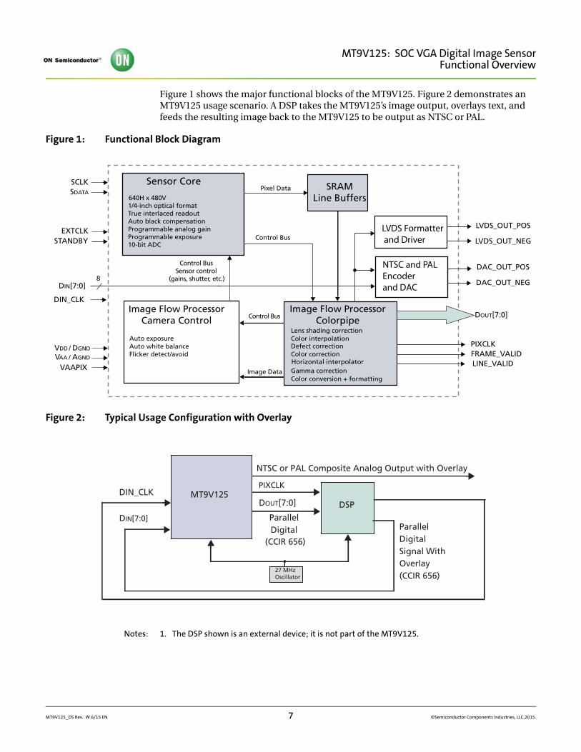
Figure 1 shows the major functional blocks of the MT9V125. Figure 2 demonstrates an MT9V125 usage scenario. A DSP takes the MT9V125’s image output, overlays text, and feeds the resulting image back to the MT9V125 to be output as NTSC or PAL.
Figure 1: Functional Block Diagram
Figure 2: Typical Usage Configuration with Overlay
Notes: 1. The DSP shown is an external device; it is not part of the MT9V125.
SRAM Line Buffers
Image Flow Processor Colorpipe
Image Flow Processor Camera Control
Image Data
Control Bus
Pixel Data SCLK SDATA
EXTCLK STANDBY
VDD / DGND
V AA / AGND
VAAPIX
Lens shading correction Color interpolation Defect correction Color correction
Gamma correction Color conversion + formatting
Auto exposure Auto white balance Flicker detect/avoid
D OUT[7:0]
PIXCLK FRAME_VALID LINE_VALID
Control Bus Sensor control
(gains, shutter, etc.)
Sensor Core 640H x 480V 1/4-inch optical format True interlaced readout Auto black compensation Programmable analog gain Programmable exposure 10-bit ADC
Control Bus
NTSC and PAL Encoder and DAC
LVDS Formatter and Driver
LVDS_OUT_POS
LVDS_OUT_NEG
DAC_OUT_POS
DAC_OUT_NEG DIN[7:0]
DIN_CLK
Horizontal interpolator
8
DSP MT9V125
Parallel Digital Signal With Overlay (CCIR 656)
NTSC or PAL Composite Analog Output with Overlay
DIN[7:0]
DOUT[7:0] DIN_CLK
Parallel Digital
(CCIR 656)
PIXCLK
27 MHz Oscillator
MT9V125_DS Rev.. W 6/15 EN 7 ©Semiconductor Components Industries, LLC,2015.
MT9V125: SOC VGA Digital Image SensorTypical Connections
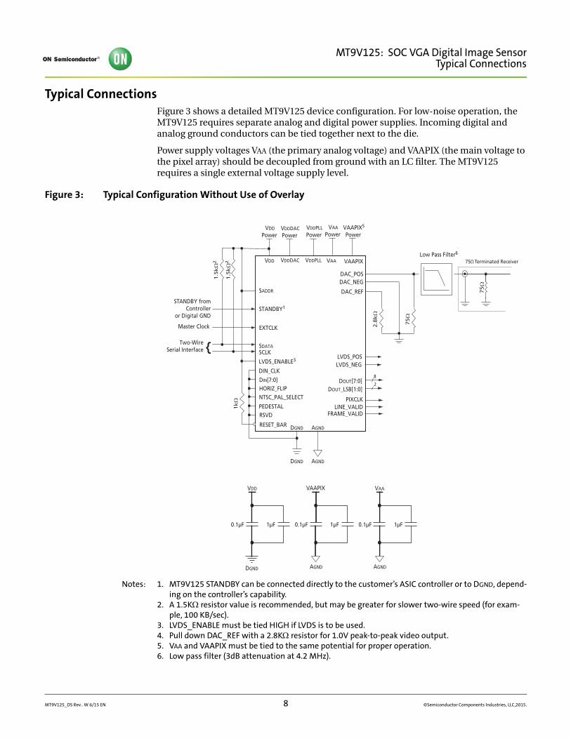
Typical ConnectionsFigure 3 shows a detailed MT9V125 device configuration. For low-noise operation, the MT9V125 requires separate analog and digital power supplies. Incoming digital and analog ground conductors can be tied together next to the die.
Power supply voltages VAA (the primary analog voltage) and VAAPIX (the main voltage to the pixel array) should be decoupled from ground with an LC filter. The MT9V125 requires a single external voltage supply level.
Figure 3: Typical Configuration Without Use of Overlay
Notes: 1. MT9V125 STANDBY can be connected directly to the customer’s ASIC controller or to DGND, depend-ing on the controller’s capability.
2. A 1.5K resistor value is recommended, but may be greater for slower two-wire speed (for exam-ple, 100 KB/sec).
3. LVDS_ENABLE must be tied HIGH if LVDS is to be used.4. Pull down DAC_REF with a 2.8K resistor for 1.0V peak-to-peak video output.5. VAA and VAAPIX must be tied to the same potential for proper operation.6. Low pass filter (3dB attenuation at 4.2 MHz).
AGND
0.1µF0.1µF
VAA
DGND
1µF
VDD VAAPIX
1µF
AGND
0.1µF 1µF
VDD
Power VAA
Power
1.5
kΩ
2
1.5
kΩ
2
SDATASCLK
RESET_BAR
LVDS_ENABLE3
FRAME_VALID
PIXCLKLINE_VALID
DOUT[7:0]
EXTCLK
SADDR
STANDBY1
1k
Ω
DGND AGND
DGND AGND
VDD VAA VAAPIX
Two-WireSerial Interface
Master Clock
STANDBY fromController
or Digital GND
PEDESTAL
NTSC_PAL_SELECTHORIZ_FLIP
DAC_NEGDAC_POS
LVDS_NEGLVDS_POS
DAC_REF
75
Ω
2.8
kΩ
DIN[7:0]
DIN_CLK
DOUT_LSB[1:0]
RSVD
75
Ω
75Ω Terminated Receiver
VDDDACPower
VDDPLLPower
VDDDAC
VDDPLL
8
2
Low Pass Filter6
VAAPIX5
Power
MT9V125_DS Rev.. W 6/15 EN 8 ©Semiconductor Components Industries, LLC,2015.
MT9V125: SOC VGA Digital Image SensorBall Assignments
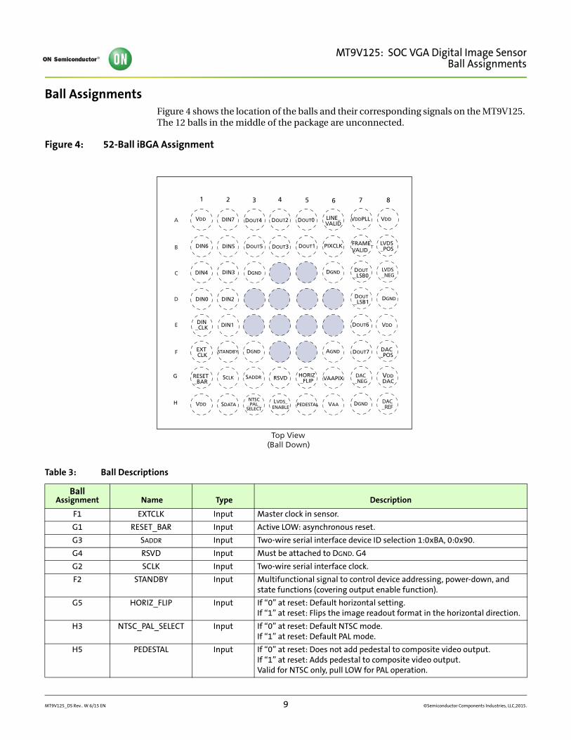
Ball AssignmentsFigure 4 shows the location of the balls and their corresponding signals on the MT9V125. The 12 balls in the middle of the package are unconnected.
Figure 4: 52-Ball iBGA Assignment
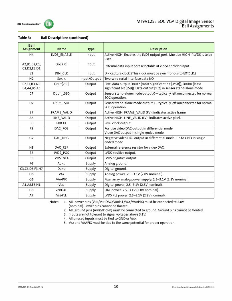
Table 3: Ball Descriptions
Ball Assignment Name Type Description
F1 EXTCLK Input Master clock in sensor.
G1 RESET_BAR Input Active LOW: asynchronous reset.
G3 SADDR Input Two-wire serial interface device ID selection 1:0xBA, 0:0x90.
G4 RSVD Input Must be attached to DGND. G4
G2 SCLK Input Two-wire serial interface clock.
F2 STANDBY Input Multifunctional signal to control device addressing, power-down, and state functions (covering output enable function).
G5 HORIZ_FLIP Input If “0” at reset: Default horizontal setting.If “1” at reset: Flips the image readout format in the horizontal direction.
H3 NTSC_PAL_SELECT Input If “0” at reset: Default NTSC mode.If “1” at reset: Default PAL mode.
H5 PEDESTAL Input If “0” at reset: Does not add pedestal to composite video output.If “1” at reset: Adds pedestal to composite video output.Valid for NTSC only, pull LOW for PAL operation.
A
B
C
D
E
F
Top View (Ball Down)
DAC _REF
DGND
G
H VDD
VDD
VDD VDD
DIN5
DIN7
DIN3
DIN2 DIN0
DIN1
DIN4
DIN6
DGND
DGND
DGND
DGND
AGND
SDATA
DOUT5 DOUT3 DOUT1
DOUT0 DOUT2 DOUT4
DOUT6
DOUT7
VDD DAC
DAC _NEG VAAPIX HORIZ
_FLIP RSVD SADDR SCLK RESET _BAR
NTSC _PAL_ SELECT
LVDS_ ENABLE PEDESTAL VAA
DAC _POS
DOUT _LSB1
DOUT _LSB0
LVDS _POS
LVDS _NEG
PIXCLK
VDDPLL LINE_ VALID
STANDBY EXTCLK
DIN _CLK
FRAME_ VALID
1 2 3 4 5 6 7 8
MT9V125_DS Rev.. W 6/15 EN 9 ©Semiconductor Components Industries, LLC,2015.
MT9V125: SOC VGA Digital Image SensorBall Assignments
Notes: 1. ALL power pins (VDD/VDDDAC/VDDPLL/VAA/VAAPIX) must be connected to 2.8V (nominal). Power pins cannot be floated.
2. ALL ground pins (AGND/DGND) must be connected to ground. Ground pins cannot be floated.3. Inputs are not tolerant to signal voltages above 3.1V.4. All unused inputs must be tied to GND or VDD.5. VAA and VAAPIX must be tied to the same potential for proper operation.
H4 LVDS_ENABLE Input Active HIGH: Enables the LVDS output port. Must be HIGH if LVDS is to be used.
A2,B1,B2,C1,C2,D2,E2,D1
DIN[7:0] Input External data input port selectable at video encoder input.
E1 DIN_CLK Input DIN capture clock. (This clock must be synchronous to EXTCLK.)
H2 SDATA Input/Output Two-wire serial interface data I/O.
F7,E7,B3,A3, B4,A4,B5,A5
DOUT[7:0] Output Pixel data output DOUT7 (most significant bit [MSB]), DOUT0 (least significant bit [LSB]). Data output [9:2] in sensor stand-alone mode
C7 DOUT_LSB0 Output Sensor stand-alone mode output 0—typically left unconnected for normal SOC operation.
D7 DOUT_LSB1 Output Sensor stand-alone mode output 1—typically left unconnected for normal SOC operation.
B7 FRAME_VALID Output Active HIGH: FRAME_VALID (FV); indicates active frame.
A6 LINE_VALID Output Active HIGH: LINE_VALID (LV); indicates active pixel.
B6 PIXCLK Output Pixel clock output.
F8 DAC_POS Output Positive video DAC output in differential mode.Video DAC output in single-ended mode.
G7 DAC_NEG Output Negative video DAC output in differential mode. Tie to GND in single-ended mode
H8 DAC_REF Output External reference resistor for video DAC.
B8 LVDS_POS Output LVDS positive output.
C8 LVDS_NEG Output LVDS negative output.
F6 AGND Supply Analog ground.
C3,C6,D8,F3,H7 DGND Supply Digital ground.
H6 VAA Supply Analog power: 2.5–3.1V (2.8V nominal).
G6 VAAPIX Supply Pixel array analog power supply: 2.5–3.1V (2.8V nominal).
A1,A8,E8,H1 VDD Supply Digital power: 2.5–3.1V (2.8V nominal).
G8 VDDDAC Supply DAC power: 2.5–3.1V (2.8V nominal).
A7 VDDPLL Supply LVDS PLL power: 2.5–3.1V (2.8V nominal).
Table 3: Ball Descriptions (continued)
Ball Assignment Name Type Description
MT9V125_DS Rev.. W 6/15 EN 10 ©Semiconductor Components Industries, LLC,2015.
MT9V125: SOC VGA Digital Image SensorDetailed Architecture Overview
Detailed Architecture Overview
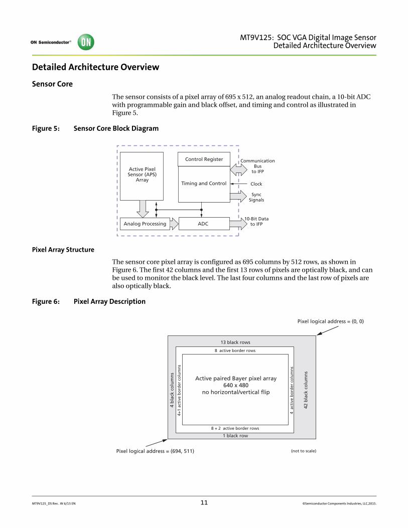
Sensor Core
The sensor consists of a pixel array of 695 x 512, an analog readout chain, a 10-bit ADC with programmable gain and black offset, and timing and control as illustrated in Figure 5.
Figure 5: Sensor Core Block Diagram
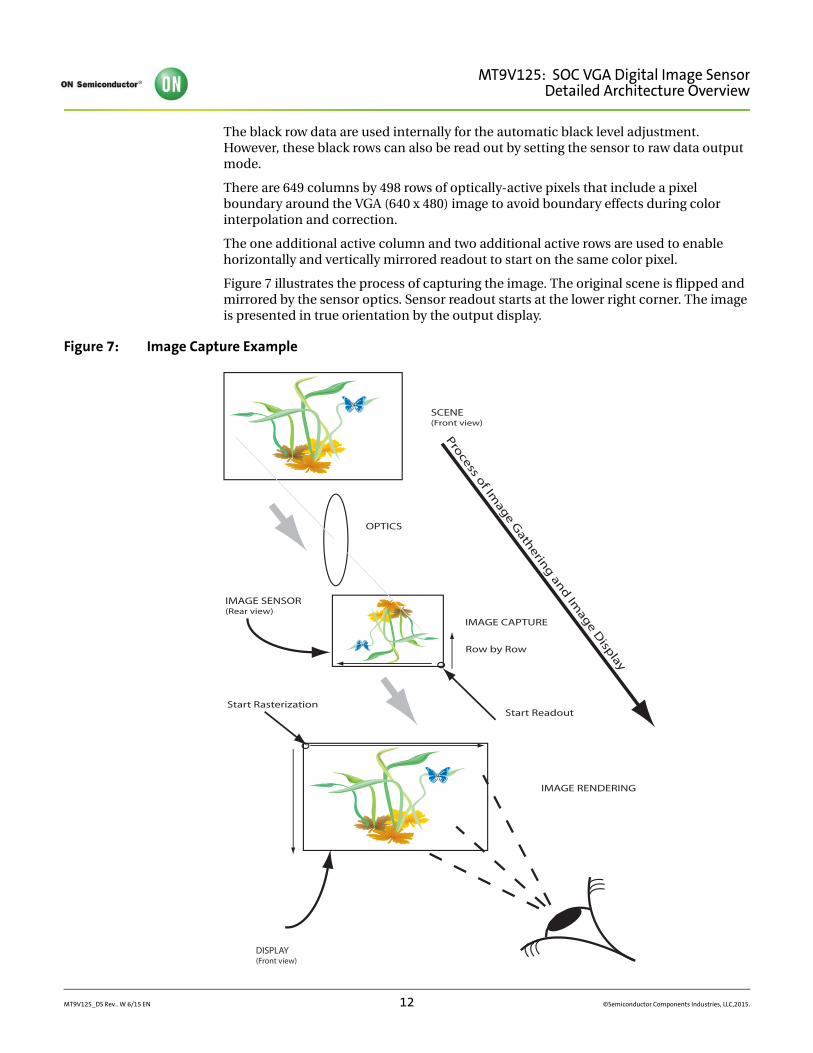
Pixel Array Structure
The sensor core pixel array is configured as 695 columns by 512 rows, as shown in Figure 6. The first 42 columns and the first 13 rows of pixels are optically black, and can be used to monitor the black level. The last four columns and the last row of pixels are also optically black.
Figure 6: Pixel Array Description
Communication Bus
to IFP
10-Bit Data to IFP
Sync Signals
Clock
Control Register
Analog Processing
Active Pixel Sensor (APS)
Array Timing and Control
ADC
8 + 2 active border rows
1 black row
13 black rows
42 b
lack
co
lum
ns
4 b
lack
co
lum
ns
8 active border rows
4 a
ctiv
e b
ord
er c
olu
mn
s
4+1
acti
ve b
ord
er c
olu
mn
s
Active paired Bayer pixel array640 x 480
no horizontal/vertical flip
(not to scale) Pixel logical address = (694, 511)
Pixel logical address = (0, 0)
MT9V125_DS Rev.. W 6/15 EN 11 ©Semiconductor Components Industries, LLC,2015.
MT9V125: SOC VGA Digital Image SensorDetailed Architecture Overview
The black row data are used internally for the automatic black level adjustment. However, these black rows can also be read out by setting the sensor to raw data output mode.
There are 649 columns by 498 rows of optically-active pixels that include a pixel boundary around the VGA (640 x 480) image to avoid boundary effects during color interpolation and correction.
The one additional active column and two additional active rows are used to enable horizontally and vertically mirrored readout to start on the same color pixel.
Figure 7 illustrates the process of capturing the image. The original scene is flipped and mirrored by the sensor optics. Sensor readout starts at the lower right corner. The image is presented in true orientation by the output display.
Figure 7: Image Capture Example
SCENE(Front view)
OPTICS
IMAGE CAPTURE
IMAGE RENDERING
Start Readout
Row by Row
IMAGE SENSOR(Rear view)
Start Rasterization
Process of Image G
athering and Image D
isplay
DISPLAY(Front view)
MT9V125_DS Rev.. W 6/15 EN 12 ©Semiconductor Components Industries, LLC,2015.
MT9V125: SOC VGA Digital Image SensorDetailed Architecture Overview
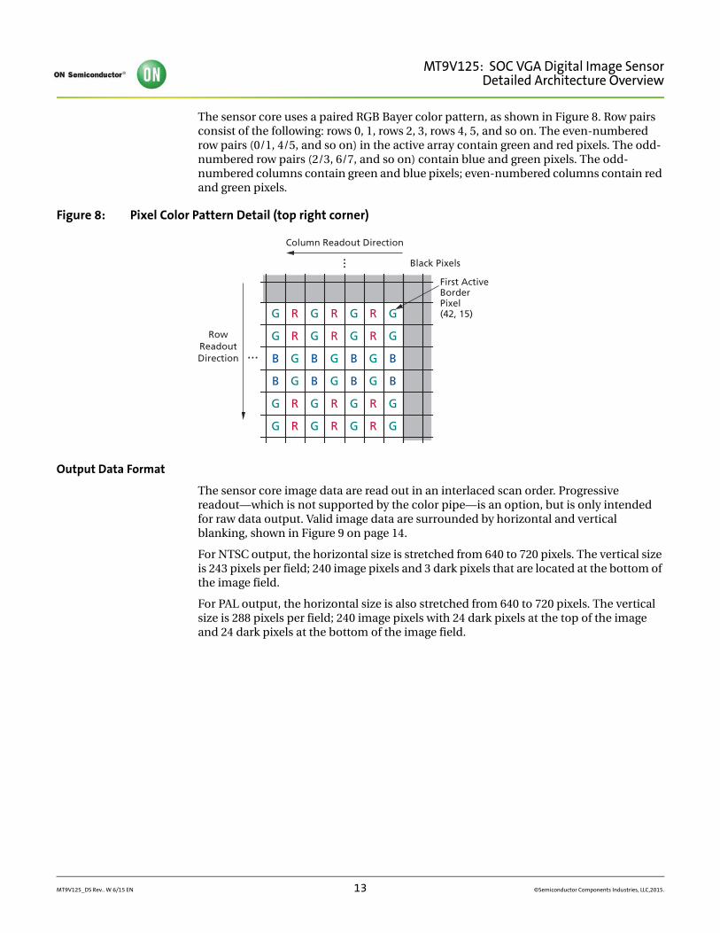
The sensor core uses a paired RGB Bayer color pattern, as shown in Figure 8. Row pairs consist of the following: rows 0, 1, rows 2, 3, rows 4, 5, and so on. The even-numbered row pairs (0/1, 4/5, and so on) in the active array contain green and red pixels. The odd-numbered row pairs (2/3, 6/7, and so on) contain blue and green pixels. The odd-numbered columns contain green and blue pixels; even-numbered columns contain red and green pixels.
Figure 8: Pixel Color Pattern Detail (top right corner)
Output Data Format
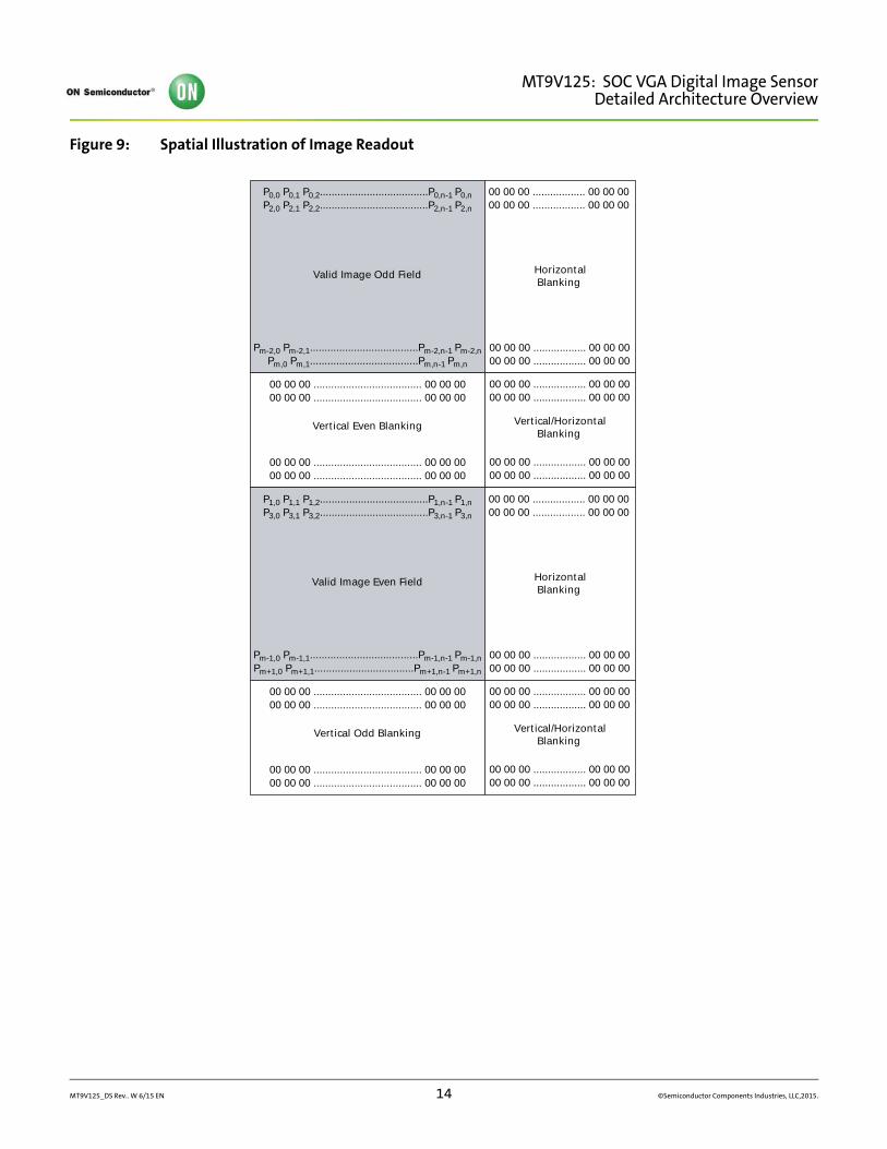
The sensor core image data are read out in an interlaced scan order. Progressive readout—which is not supported by the color pipe—is an option, but is only intended for raw data output. Valid image data are surrounded by horizontal and vertical blanking, shown in Figure 9 on page 14.
For NTSC output, the horizontal size is stretched from 640 to 720 pixels. The vertical size is 243 pixels per field; 240 image pixels and 3 dark pixels that are located at the bottom of the image field.
For PAL output, the horizontal size is also stretched from 640 to 720 pixels. The vertical size is 288 pixels per field; 240 image pixels with 24 dark pixels at the top of the image and 24 dark pixels at the bottom of the image field.
Black Pixels
Column Readout Direction
. . .
...
Row Readout Direction
R
R
G
G
R
R
G
G
B
B
G
G
First ActiveBorderPixel(42, 15)R
R
G
G
R
R
G
G
B
B
G
G
R
R
G
G
R
R
G
G
B
B
G
G
G
G
B
B
G
G
MT9V125_DS Rev.. W 6/15 EN 13 ©Semiconductor Components Industries, LLC,2015.
MT9V125: SOC VGA Digital Image SensorDetailed Architecture Overview
Figure 9: Spatial Illustration of Image Readout
P0,0 P0,1 P0,2.....................................P0,n-1 P0,nP2,0 P2,1 P2,2.....................................P2,n-1 P2,n
00 00 00 .................. 00 00 0000 00 00 .................. 00 00 00
Pm-2,0 Pm-2,1.....................................Pm-2,n-1 Pm-2,nPm,0 Pm,1.....................................Pm,n-1 Pm,n
00 00 00 .................. 00 00 0000 00 00 .................. 00 00 00
00 00 00 .................. 00 00 0000 00 00 .................. 00 00 00
00 00 00 .................. 00 00 0000 00 00 .................. 00 00 00
00 00 00 ..................................... 00 00 0000 00 00 ..................................... 00 00 00
00 00 00 ..................................... 00 00 0000 00 00 ..................................... 00 00 00
Valid Image Odd Field HorizontalBlanking
Vertical Even Blanking Vertical/HorizontalBlanking
P1,0 P1,1 P1,2.....................................P1,n-1 P1,nP3,0 P3,1 P3,2.....................................P3,n-1 P3,n
00 00 00 .................. 00 00 0000 00 00 .................. 00 00 00
Pm-1,0 Pm-1,1.....................................Pm-1,n-1 Pm-1,nPm+1,0 Pm+1,1..................................Pm+1,n-1 Pm+1,n
00 00 00 .................. 00 00 0000 00 00 .................. 00 00 00
00 00 00 .................. 00 00 0000 00 00 .................. 00 00 00
00 00 00 .................. 00 00 0000 00 00 .................. 00 00 00
00 00 00 ..................................... 00 00 0000 00 00 ..................................... 00 00 00
00 00 00 ..................................... 00 00 0000 00 00 ..................................... 00 00 00
Valid Image Even Field HorizontalBlanking
Vertical Odd Blanking Vertical/HorizontalBlanking
MT9V125_DS Rev.. W 6/15 EN 14 ©Semiconductor Components Industries, LLC,2015.
MT9V125: SOC VGA Digital Image SensorDetailed Architecture Overview
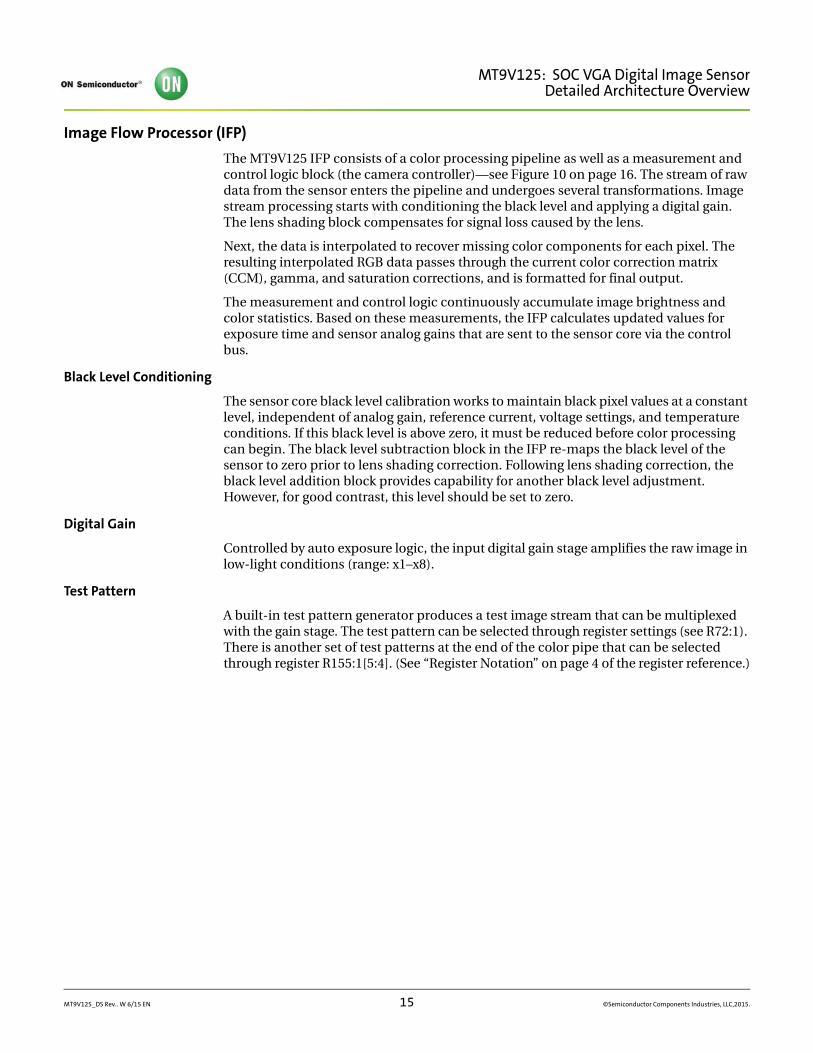
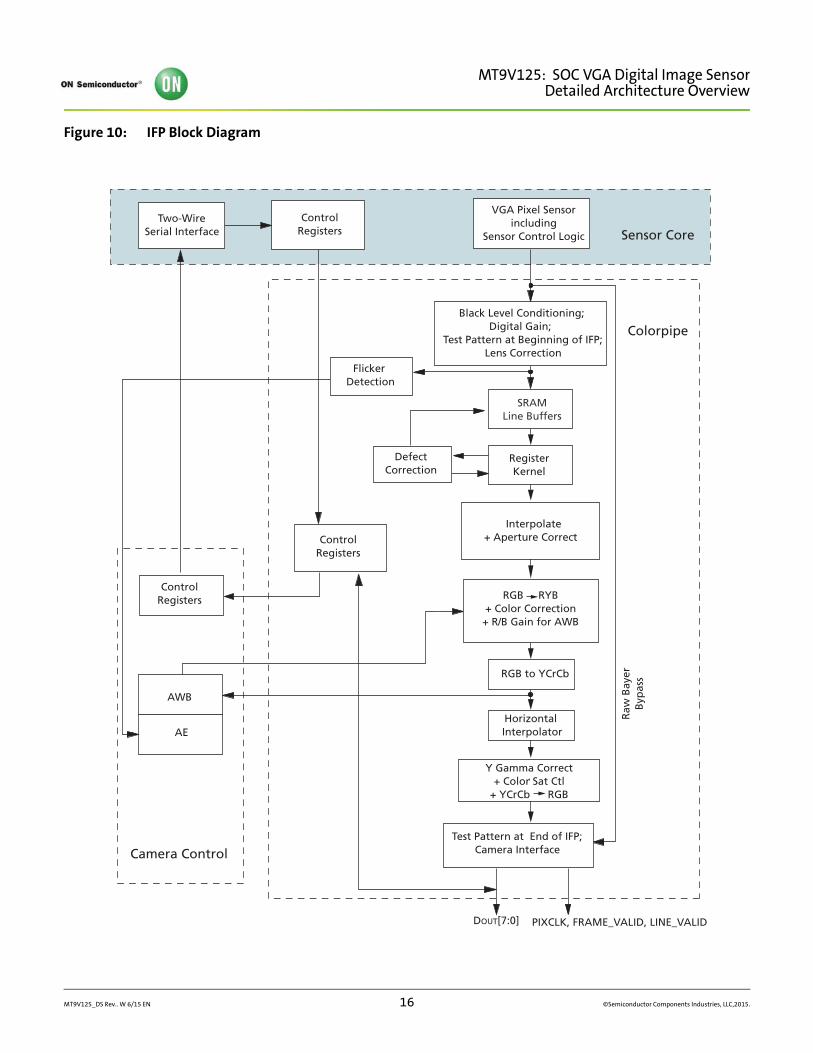
Image Flow Processor (IFP)
The MT9V125 IFP consists of a color processing pipeline as well as a measurement and control logic block (the camera controller)—see Figure 10 on page 16. The stream of raw data from the sensor enters the pipeline and undergoes several transformations. Image stream processing starts with conditioning the black level and applying a digital gain. The lens shading block compensates for signal loss caused by the lens.
Next, the data is interpolated to recover missing color components for each pixel. The resulting interpolated RGB data passes through the current color correction matrix (CCM), gamma, and saturation corrections, and is formatted for final output.
The measurement and control logic continuously accumulate image brightness and color statistics. Based on these measurements, the IFP calculates updated values for exposure time and sensor analog gains that are sent to the sensor core via the control bus.
Black Level Conditioning
The sensor core black level calibration works to maintain black pixel values at a constant level, independent of analog gain, reference current, voltage settings, and temperature conditions. If this black level is above zero, it must be reduced before color processing can begin. The black level subtraction block in the IFP re-maps the black level of the sensor to zero prior to lens shading correction. Following lens shading correction, the black level addition block provides capability for another black level adjustment. However, for good contrast, this level should be set to zero.
Digital Gain
Controlled by auto exposure logic, the input digital gain stage amplifies the raw image in low-light conditions (range: x1–x8).
Test Pattern
A built-in test pattern generator produces a test image stream that can be multiplexed with the gain stage. The test pattern can be selected through register settings (see R72:1). There is another set of test patterns at the end of the color pipe that can be selected through register R155:1[5:4]. (See “Register Notation” on page 4 of the register reference.)
MT9V125_DS Rev.. W 6/15 EN 15 ©Semiconductor Components Industries, LLC,2015.
MT9V125: SOC VGA Digital Image SensorDetailed Architecture Overview
Figure 10: IFP Block Diagram
Sensor Core
Colorpipe
Camera Control
DOUT[7:0] PIXCLK, FRAME_VALID, LINE_VALID
Raw
Bay
erB
ypas
s
Y Gamma Correct+ Color Sat Ctl
+ YCrCb RGB
Horizontal Interpolator
RGB to YCrCb
RGB RYB+ Color Correction
+ R/B Gain for AWB
Interpolate
+ Aperture Correct
RegisterKernel
SRAMLine Buffers
DefectCorrection
Flicker Detection
Black Level Conditioning; Digital Gain;
Test Pattern at Beginning of IFP;Lens Correction
VGA Pixel Sensorincluding
Sensor Control Logic
ControlRegisters
Two-WireSerial Interface
ControlRegisters
AE
AWB
Test Pattern at End of IFP;Camera Interface
ControlRegisters
MT9V125_DS Rev.. W 6/15 EN 16 ©Semiconductor Components Industries, LLC,2015.
MT9V125: SOC VGA Digital Image SensorDetailed Architecture Overview
Notes: 1. NTSC encoder/DAC not shown
Lens Shading Correction (LC)
Inexpensive lenses tend to attenuate image intensity near the edges of pixel arrays. Other factors also cause signal and coloration differences across the image. The net result of all these factors is known as lens shading. Lens shading correction (LC) compensates for these differences.
Typically, the profile of lens shading-induced anomalies across the frame is different for each color component. Therefore, LC is independently calibrated for the color channels.
Interpolation and Aperture Correction
A demosaic engine converts the single-color-per-pixel Bayer data from the sensor into RGB (10-bit per color channel). The demosaic algorithm analyzes neighboring pixels to generate a best guess for the missing color components. Edge sharpness is preserved as much as possible.
Aperture correction sharpens the image by an adjustable amount. To avoid amplifying noise, sharpening can be programmed to phase out as light levels drop.
Defect Correction
This device supports 2D defect correction. In 2D defect detection and correction, pixels with values different from their neighbors by greater than a defined threshold are considered defects unless near the image boundary. The approach is termed 2D, as pixels on neighboring lines as well as neighboring pixels on the same line are considered in both detection and correction.
In Figure 10 on page 16, the register kernel gathers same color pixels and send the infor-mation to the 2D defect correction engine.
Color Correction
To obtain good color rendition and saturation, it is necessary to compensate for the differences between the spectral characteristics of the imager color filter array and the spectral response of the human eye. This compensation, also known as color separation, is achieved through linear transformation of the image with a 3 x 3 element color correc-tion matrix. The optimal values for the color correction coefficients depend on the spectra of the incident illumination and can be programmed by the user.
Color Saturation Control
For noise reduction, both color saturation and sharpness enhancement can be set by the user or adjusted automatically by tracking the magnitude of the gains used by the auto exposure algorithm.
Automatic White Balance (AWB)
The MT9V125 has a built-in AWB algorithm designed to compensate for the effects of changing scene illumination on the color rendition quality. This sophisticated algorithm consists of three major submodules: • A measurement engine (ME) performing statistical analysis of the image• A module selecting the optimal color correction matrix• A module selecting the analog color channel gains in the sensor core
MT9V125_DS Rev.. W 6/15 EN 17 ©Semiconductor Components Industries, LLC,2015.
MT9V125: SOC VGA Digital Image SensorDetailed Architecture Overview
While the default algorithm settings are adequate in most situations, the user can repro-gram base color correction matrices and limit color channel gains. The AWB does not attempt to locate the brightest or grayest elements in the image; it performs in-depth image analysis to differentiate between changes in predominant spectra of illumination and changes in predominant scene colors. Factory defaults are suitable for most appli-cations; however, a wide range of algorithm parameters can be overwritten by the user through the serial interface.
AWB Measurment Window
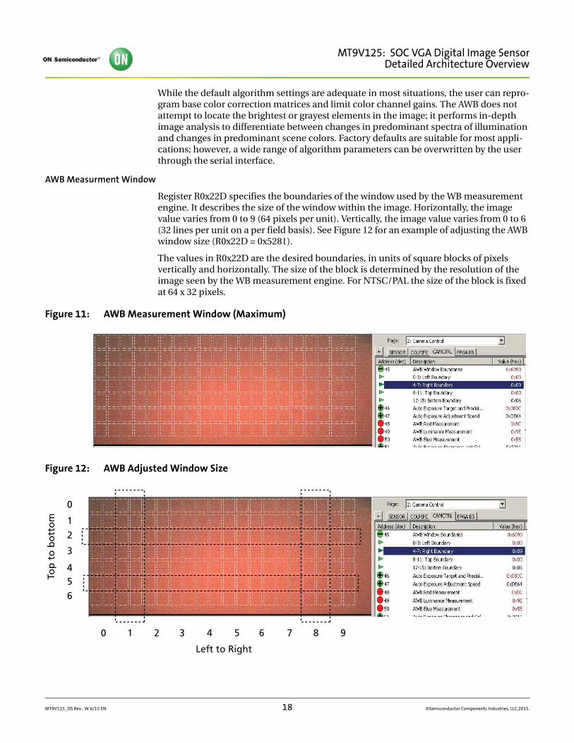
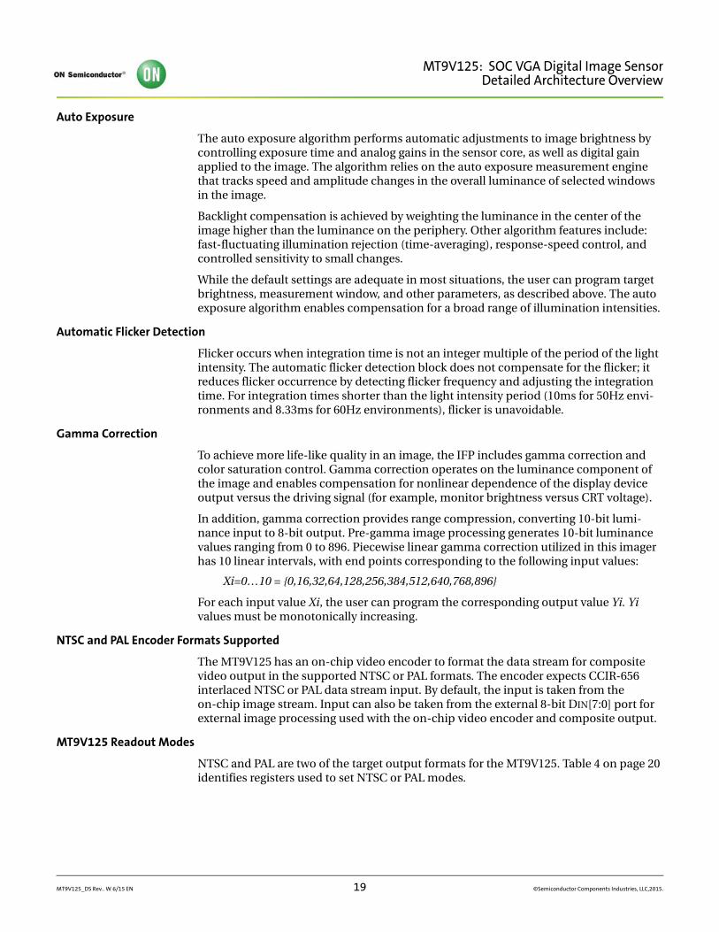
Register R0x22D specifies the boundaries of the window used by the WB measurement engine. It describes the size of the window within the image. Horizontally, the image value varies from 0 to 9 (64 pixels per unit). Vertically, the image value varies from 0 to 6 (32 lines per unit on a per field basis). See Figure 12 for an example of adjusting the AWB window size (R0x22D = 0x5281).
The values in R0x22D are the desired boundaries, in units of square blocks of pixels vertically and horizontally. The size of the block is determined by the resolution of the image seen by the WB measurement engine. For NTSC/PAL the size of the block is fixed at 64 x 32 pixels.
Figure 11: AWB Measurement Window (Maximum)
Figure 12: AWB Adjusted Window Size
0
12
3
456
0 1 2 3 4 5 6 7 8 9
Left to Right
Top
to
bo
tto
m
MT9V125_DS Rev.. W 6/15 EN 18 ©Semiconductor Components Industries, LLC,2015.
MT9V125: SOC VGA Digital Image SensorDetailed Architecture Overview
Auto Exposure
The auto exposure algorithm performs automatic adjustments to image brightness by controlling exposure time and analog gains in the sensor core, as well as digital gain applied to the image. The algorithm relies on the auto exposure measurement engine that tracks speed and amplitude changes in the overall luminance of selected windows in the image.
Backlight compensation is achieved by weighting the luminance in the center of the image higher than the luminance on the periphery. Other algorithm features include: fast-fluctuating illumination rejection (time-averaging), response-speed control, and controlled sensitivity to small changes.
While the default settings are adequate in most situations, the user can program target brightness, measurement window, and other parameters, as described above. The auto exposure algorithm enables compensation for a broad range of illumination intensities.
Automatic Flicker Detection
Flicker occurs when integration time is not an integer multiple of the period of the light intensity. The automatic flicker detection block does not compensate for the flicker; it reduces flicker occurrence by detecting flicker frequency and adjusting the integration time. For integration times shorter than the light intensity period (10ms for 50Hz envi-ronments and 8.33ms for 60Hz environments), flicker is unavoidable.
Gamma Correction
To achieve more life-like quality in an image, the IFP includes gamma correction and color saturation control. Gamma correction operates on the luminance component of the image and enables compensation for nonlinear dependence of the display device output versus the driving signal (for example, monitor brightness versus CRT voltage).
In addition, gamma correction provides range compression, converting 10-bit lumi-nance input to 8-bit output. Pre-gamma image processing generates 10-bit luminance values ranging from 0 to 896. Piecewise linear gamma correction utilized in this imager has 10 linear intervals, with end points corresponding to the following input values:
Xi=0…10 = {0,16,32,64,128,256,384,512,640,768,896}
For each input value Xi, the user can program the corresponding output value Yi. Yi values must be monotonically increasing.
NTSC and PAL Encoder Formats Supported
The MT9V125 has an on-chip video encoder to format the data stream for composite video output in the supported NTSC or PAL formats. The encoder expects CCIR-656 interlaced NTSC or PAL data stream input. By default, the input is taken from the on-chip image stream. Input can also be taken from the external 8-bit DIN[7:0] port for external image processing used with the on-chip video encoder and composite output.
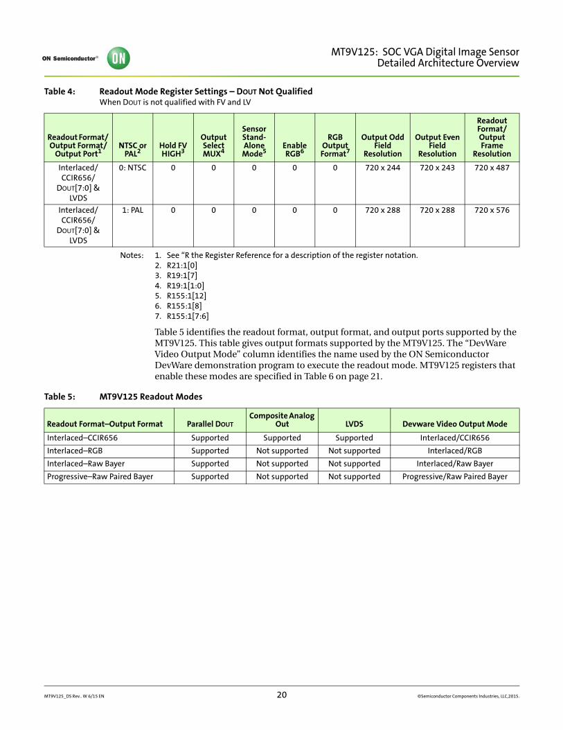
MT9V125 Readout Modes
NTSC and PAL are two of the target output formats for the MT9V125. Table 4 on page 20 identifies registers used to set NTSC or PAL modes.
MT9V125_DS Rev.. W 6/15 EN 19 ©Semiconductor Components Industries, LLC,2015.
MT9V125: SOC VGA Digital Image SensorDetailed Architecture Overview
Notes: 1. See “R the Register Reference for a description of the register notation.2. R21:1[0]3. R19:1[7]4. R19:1[1:0]5. R155:1[12]6. R155:1[8]7. R155:1[7:6]
Table 5 identifies the readout format, output format, and output ports supported by the MT9V125. This table gives output formats supported by the MT9V125. The “DevWare Video Output Mode” column identifies the name used by the ON Semiconductor DevWare demonstration program to execute the readout mode. MT9V125 registers that enable these modes are specified in Table 6 on page 21.
Table 4: Readout Mode Register Settings – DOUT Not QualifiedWhen DOUT is not qualified with FV and LV
Readout Format/ Output Format/
Output Port1NTSC or
PAL2Hold FV HIGH3
Output Select MUX4
Sensor Stand- Alone Mode5
Enable RGB6
RGB Output Format7
Output Odd Field
Resolution
Output Even Field
Resolution
Readout Format/ Output Frame
Resolution
Interlaced/CCIR656/
DOUT[7:0] & LVDS
0: NTSC 0 0 0 0 0 720 x 244 720 x 243 720 x 487
Interlaced/CCIR656/
DOUT[7:0] & LVDS
1: PAL 0 0 0 0 0 720 x 288 720 x 288 720 x 576
Table 5: MT9V125 Readout Modes
Readout Format–Output Format Parallel DOUTComposite Analog
Out LVDS Devware Video Output Mode
Interlaced–CCIR656 Supported Supported Supported Interlaced/CCIR656
Interlaced–RGB Supported Not supported Not supported Interlaced/RGB
Interlaced–Raw Bayer Supported Not supported Not supported Interlaced/Raw Bayer
Progressive–Raw Paired Bayer Supported Not supported Not supported Progressive/Raw Paired Bayer
MT9V125_DS Rev.. W 6/15 EN 20 ©Semiconductor Components Industries, LLC,2015.
MT9V125: SOC VGA Digital Image SensorDetailed Architecture Overview
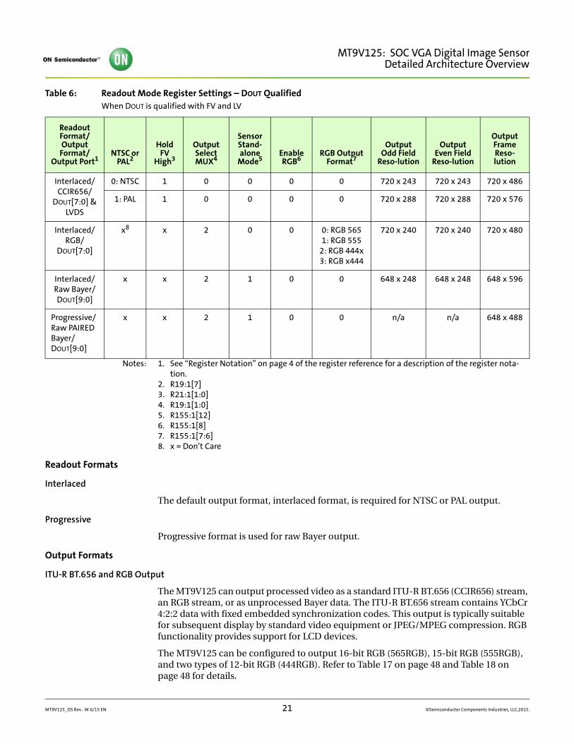
Table 6: Readout Mode Register Settings – DOUT QualifiedWhen DOUT is qualified with FV and LV
Notes: 1. See “Register Notation” on page 4 of the register reference for a description of the register nota-tion.
2. R19:1[7]3. R21:1[1:0]4. R19:1[1:0]5. R155:1[12]6. R155:1[8]7. R155:1[7:6]8. x = Don’t Care
Readout Formats
Interlaced
The default output format, interlaced format, is required for NTSC or PAL output.
Progressive
Progressive format is used for raw Bayer output.
Output Formats
ITU-R BT.656 and RGB Output
The MT9V125 can output processed video as a standard ITU-R BT.656 (CCIR656) stream, an RGB stream, or as unprocessed Bayer data. The ITU-R BT.656 stream contains YCbCr 4:2:2 data with fixed embedded synchronization codes. This output is typically suitable for subsequent display by standard video equipment or JPEG/MPEG compression. RGB functionality provides support for LCD devices.
The MT9V125 can be configured to output 16-bit RGB (565RGB), 15-bit RGB (555RGB), and two types of 12-bit RGB (444RGB). Refer to Table 17 on page 48 and Table 18 on page 48 for details.
Readout Format/ Output
Format/Output Port1
NTSC or PAL2
Hold FV
High3
Output Select MUX4
Sensor Stand-alone
Mode5Enable RGB6
RGB Output Format7
Output Odd Field
Reso-lution
Output Even Field
Reso-lution
Output Frame Reso-lution
Interlaced/ CCIR656/
DOUT[7:0] & LVDS
0: NTSC 1 0 0 0 0 720 x 243 720 x 243 720 x 486
1: PAL 1 0 0 0 0 720 x 288 720 x 288 720 x 576
Interlaced/RGB/
DOUT[7:0]
x8 x 2 0 0 0: RGB 5651: RGB 555
2: RGB 444x3: RGB x444
720 x 240 720 x 240 720 x 480
Interlaced/Raw Bayer/DOUT[9:0]
x x 2 1 0 0 648 x 248 648 x 248 648 x 596
Progressive/Raw PAIRED Bayer/DOUT[9:0]
x x 2 1 0 0 n/a n/a 648 x 488
MT9V125_DS Rev.. W 6/15 EN 21 ©Semiconductor Components Industries, LLC,2015.
MT9V125: SOC VGA Digital Image SensorDetailed Architecture Overview
Bayer Output
Unprocessed paired Bayer data are generated when bypassing the IFP completely—that is, by simply outputting the sensor-paired Bayer stream as usual, using FV, LV, and PIXCLK to time the data. This mode is called sensor stand-alone mode.
Output Ports
Composite Video Output
The composite video output DAC is external-resistor-programmable and supports both single-ended and differential output. The DAC is driven by the on-chip video encoder output.
Serial Data Output
The processed image data stream can be output to the LVDS output port.
Parallel Output
Parallel output uses either 8-bit or 10-bit output. Eight-bit output is used for ITU-R BT.656 and RGB output. Ten-bit output is used for raw Bayer output.
MT9V125_DS Rev.. W 6/15 EN 22 ©Semiconductor Components Industries, LLC,2015.
MT9V125: SOC VGA Digital Image SensorDetailed Architecture Overview
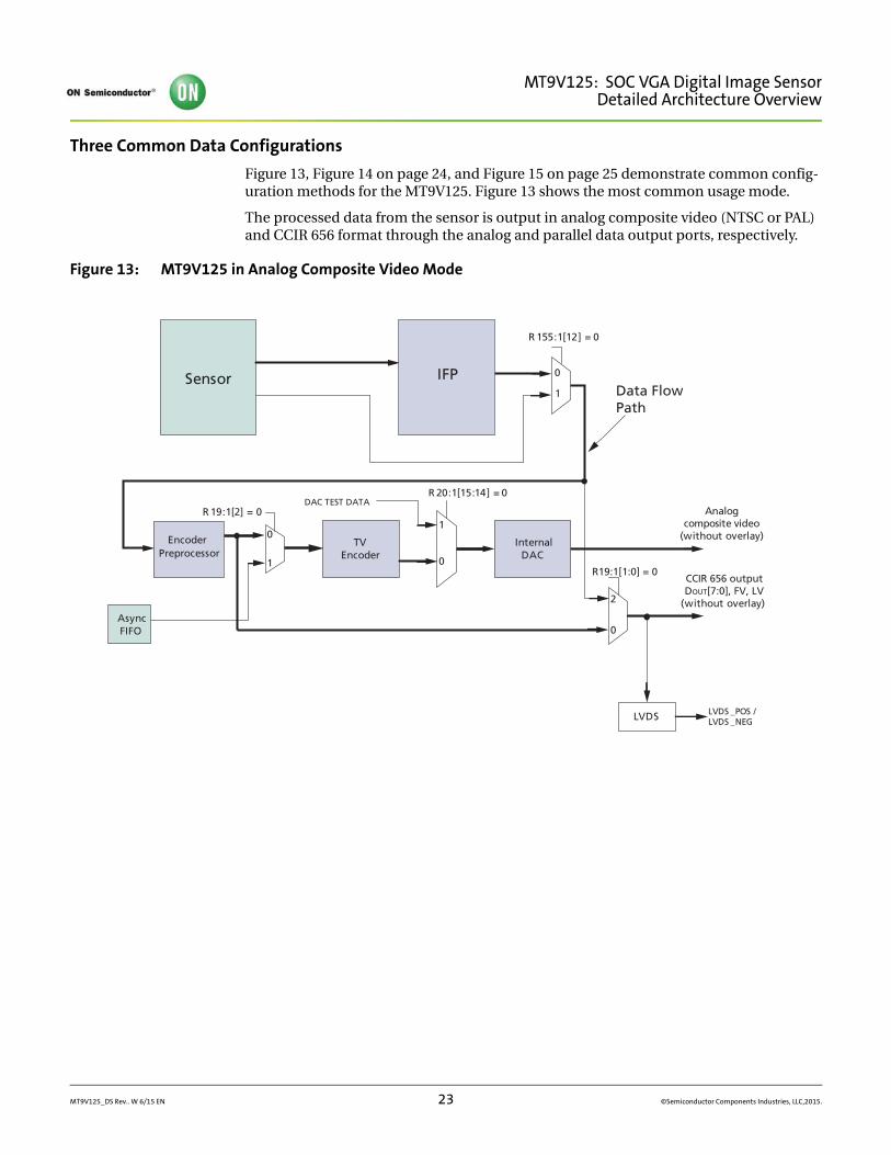
Three Common Data Configurations
Figure 13, Figure 14 on page 24, and Figure 15 on page 25 demonstrate common config-uration methods for the MT9V125. Figure 13 shows the most common usage mode.
The processed data from the sensor is output in analog composite video (NTSC or PAL) and CCIR 656 format through the analog and parallel data output ports, respectively.
Figure 13: MT9V125 in Analog Composite Video Mode
TVEncoder
DAC TEST DATA
InternalDAC
CCIR 656 outputDOUT[7:0], FV, LV
(without overlay)
Analogcomposite video
(without overlay)
LVDS LVDS _POS /LVDS _NEG
0
2
0
1
1
0
R 20:1[15:14] = 0
R 19:1[2] = 0
AsyncFIFO
R 155:1[12] = 0
1
0
Data FlowPath
Sensor IFP
Encoder Preprocessor
R19:1[1:0] = 0
MT9V125_DS Rev.. W 6/15 EN 23 ©Semiconductor Components Industries, LLC,2015.
MT9V125: SOC VGA Digital Image SensorDetailed Architecture Overview
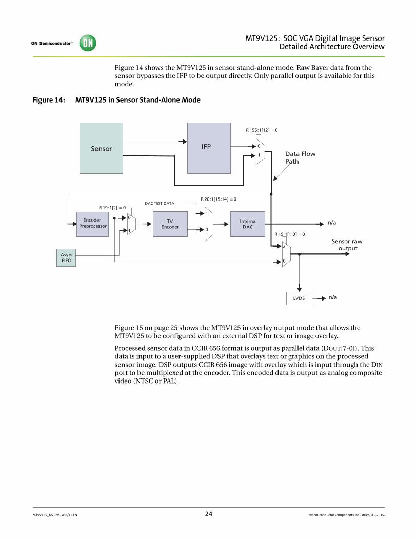
Figure 14 shows the MT9V125 in sensor stand-alone mode. Raw Bayer data from the sensor bypasses the IFP to be output directly. Only parallel output is available for this mode.
Figure 14: MT9V125 in Sensor Stand-Alone Mode
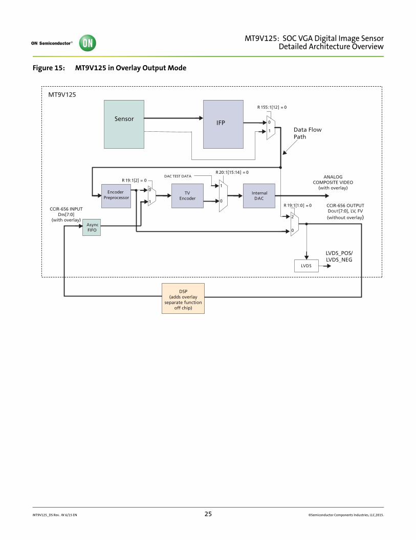
Figure 15 on page 25 shows the MT9V125 in overlay output mode that allows the MT9V125 to be configured with an external DSP for text or image overlay.
Processed sensor data in CCIR 656 format is output as parallel data (DOUT[7-0]). This data is input to a user-supplied DSP that overlays text or graphics on the processed sensor image. DSP outputs CCIR 656 image with overlay which is input through the DIN port to be multiplexed at the encoder. This encoded data is output as analog composite video (NTSC or PAL).
TVEncoder
DAC TEST DATA
InternalDAC
LVDS
0
2
0
1
1
0
R 19:1[1:0] = 0
R 20:1[15:14] = 0
R 19:1[2] = 0
AsyncFIFO
R 155:1[12] = 0
1
0
Data FlowPath
Sensor IFP
Encoder Preprocessor
Sensor raw output
n/a
n/a
MT9V125_DS Rev.. W 6/15 EN 24 ©Semiconductor Components Industries, LLC,2015.
MT9V125: SOC VGA Digital Image SensorDetailed Architecture Overview
Figure 15: MT9V125 in Overlay Output Mode
TVEncoder
DAC TEST DATA
InternalDAC
LVDS
0
2
0
1
1
0
R 19:1[1:0] = 0
R 20:1[15:14] = 0
R 19:1[2] = 0
AsyncFIFO
R 155:1[12] = 0
1
0
Data FlowPath
IFP
Encoder Preprocessor
CCIR-656 OUTPUTDOUT[7:0], LV, FV(without overlay)
ANALOGCOMPOSITE VIDEO
(with overlay)
LVDS_POS/LVDS_NEG
CCIR-656 INPUTDIN[7:0]
(with overlay)
DSP(adds overlay
separate functionoff chip)
MT9V125
Sensor
MT9V125_DS Rev.. W 6/15 EN 25 ©Semiconductor Components Industries, LLC,2015.
MT9V125: SOC VGA Digital Image SensorSensor Core Modes and Timing
Sensor Core Modes and Timing This section provides an overview of usage modes for the MT9V125 sensor core. An over-view of typical usage modes for the complete MT9V125 is provided in “Modes and Timing” on page 33.
Readout Format
The sensor core supports two basic readout formats: interlaced and progressive. The interlaced format supports both NTSC and PAL timing. Progressive readout is intended for sensor stand-alone mode only (this is due to the paired Bayer pattern CFA).
Window Control
The window size and position need to be at the default settings for correct NTSC or PAL format support.
Window Start
The row and column start address of the displayed image can be set by R1:0 (row start) and R2:0 (column start).
Window Size
The default sensor resolution is 640 columns and 480 rows (VGA). For NTSC and PAL, this is expanded by the horizontal interpolator module to 720 columns. For proper NTSC or PAL operation, use only the default window size.
Pixel Border
When R32:0, Bits[9:8] are both set, a 4-pixel border will be added around the specified image. When enabled, the row and column widths will be 8 pixels larger than the values programmed in the row and column registers. If the border is enabled but not shown in the image (R32:0[9:8] = 01), the horizontal blanking and vertical blanking values will be 8 pixels larger than the values programmed into the blanking registers. For proper NTSC or PAL operation, use only default values in the above mentioned registers.
The border is read in an interlaced pattern when in interlaced readout mode. Each field has its own interlaced border on top and bottom of the active array.
Sensor Core Readout Modes
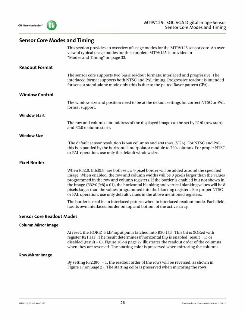
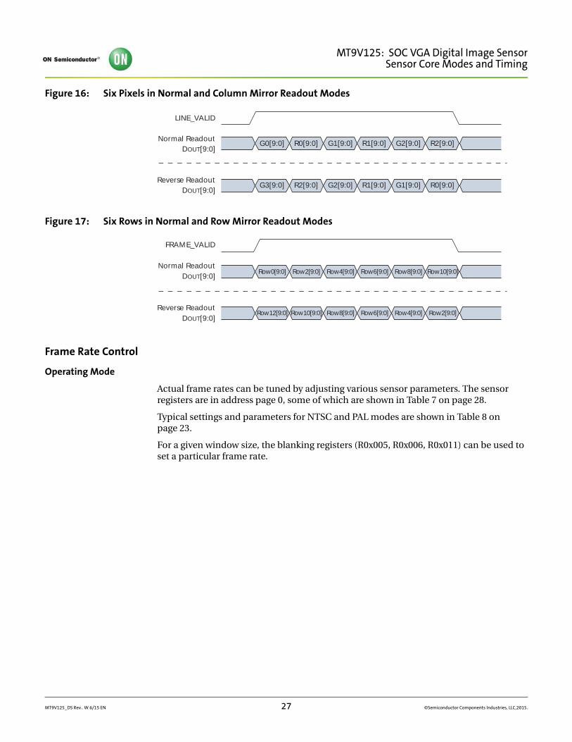
Column Mirror Image
At reset, the HORIZ_FLIP input pin is latched into R30:1[1]. This bit is XORed with register R21:1[1]. The result determines if horizontal flip is enabled (result = 1) or disabled (result = 0). Figure 16 on page 27 illustrates the readout order of the columns when they are reversed. The starting color is preserved when mirroring the columns.
Row Mirror Image
By setting R32:0[0] = 1, the readout order of the rows will be reversed, as shown in Figure 17 on page 27. The starting color is preserved when mirroring the rows.
MT9V125_DS Rev.. W 6/15 EN 26 ©Semiconductor Components Industries, LLC,2015.
MT9V125: SOC VGA Digital Image SensorSensor Core Modes and Timing
Figure 16: Six Pixels in Normal and Column Mirror Readout Modes
Figure 17: Six Rows in Normal and Row Mirror Readout Modes
Frame Rate Control
Operating Mode
Actual frame rates can be tuned by adjusting various sensor parameters. The sensor registers are in address page 0, some of which are shown in Table 7 on page 28.
Typical settings and parameters for NTSC and PAL modes are shown in Table 8 on page 23.
For a given window size, the blanking registers (R0x005, R0x006, R0x011) can be used to set a particular frame rate.
G0[9:0] R0[9:0] G1[9:0] R1[9:0] G2[9:0] R2[9:0]
G3[9:0] R2[9:0] G2[9:0] R1[9:0] G1[9:0] R0[9:0]
LINE_VALID
Normal ReadoutDOUT[9:0]
Reverse ReadoutDOUT[9:0]
Row0[9:0] Row2[9:0] Row4[9:0] Row6[9:0] Row8[9:0] Row10[9:0]
Row12[9:0] Row10[9:0] Row8[9:0] Row6[9:0] Row4[9:0] Row2[9:0]
FRAME_VALID
Normal ReadoutDOUT[9:0]
Reverse ReadoutDOUT[9:0]
MT9V125_DS Rev.. W 6/15 EN 27 ©Semiconductor Components Industries, LLC,2015.
MT9V125: SOC VGA Digital Image SensorSensor Core Modes and Timing
The sensor timing (Table 8 on page 28) is shown in terms of pixel clock and master clock cycles. The required master clock frequency is 27 MHz. The vertical blanking and total frame time equations assume that the number of integration rows (R0x009) is less than the number of active rows, plus blanking rows. If this is not the case, the number of inte-gration rows must be used instead to determine the frame time.
In the MT9V125, the sensor core adds four border pixels all the way around the image, taking the active image size to 648 x 488. This is achieved through the default of oversize and show border bits set.
NTSC mode has 525 rows per frame; PAL mode has 625 rows per frame as enumerated below (all values in rows):
(EQ 1)
NTSC: (EQ 2)
PAL: (EQ 3)
Blanking Calculations
When calculating blanking, minimum values for horizontal blanking and vertical blanking must be taken into account. Table 8 shows minimum values for each register. This is valid for non NTSC or PAL modes only.
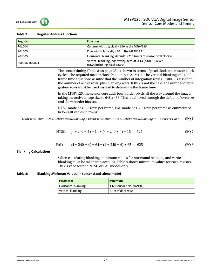
Table 7: Register Address Functions
Register Function
R0x004 Column width, typically 640 in the MT9V125
R0x003 Row width, typically 480 in the MT9V125
R0x005 Horizontal blanking, default is 210 (units of sensor pixel clocks)
R0x006, R0x011Vertical blanking (odd/even), default is 14 (odd), 15 (even) (rows including black rows)
Table 8: Blanking Minimum Values (in sensor stand-alone mode)
Parameter Minimum
Horizontal blanking 132 (sensor pixel clocks)
Vertical blanking 6 + # of dark rows
OddFieldActive OddFieldVerticalBlanking EvenFieldActive EvenFieldVerticalBlanking+ + + RowsPerFrame=
(4 240 4) 14 (4 240 4) 15+ + + + + + + 525=
(4 240 4) 64 (4 240 4) 65+ + + + + + + 625=
MT9V125_DS Rev.. W 6/15 EN 28 ©Semiconductor Components Industries, LLC,2015.
MT9V125: SOC VGA Digital Image SensorSensor Core Modes and Timing
Minimum Horizontal Blanking (in sensor stand-alone mode)
The minimum horizontal blanking value is constrained by the time used for sampling a row of pixels and the overhead in the row readout. This can be expressed in an equation as:
(EQ 4)
(EQ 5)
(EQ 6)
where:
(EQ 7)
(EQ 8)
with default settings:
To get an aggressive minimum value for the horizontal blanking, the larger of R0x079[15:8] and R0x076[15:8] can be substituted for the R0x07E value in the above equation. With default settings, this gives a minimum HBLANK time of 127.
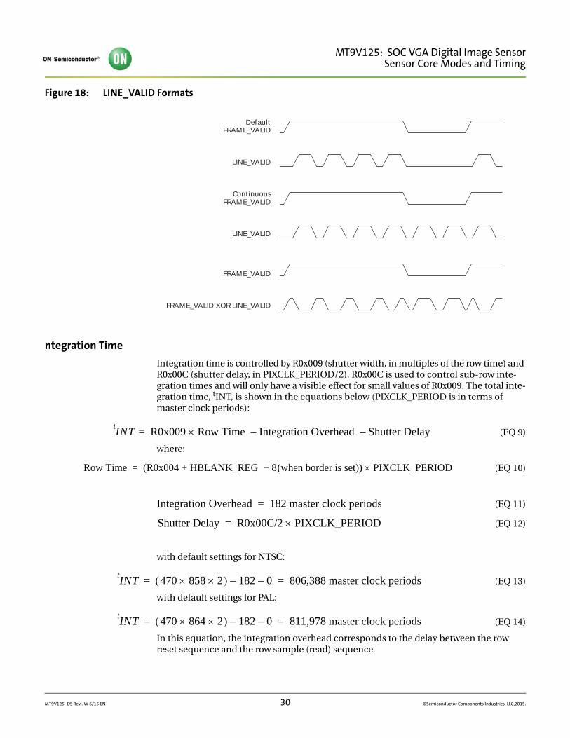
Valid Data Signals Options
LINE_VALID Signal
By setting bits[15:14] of R32:0, the LV signal is programmed for three different output formats. The formats shown below illustrate reading out four rows and two vertical blanking rows (Figure 18 on page 30).
The default line valid format is shown first; continuous line valid is shown second. In the last format, the LV signal is exclusive ORed (XOR) between the continuous LV signal and the FV signal.
HBLANK(min) (startup overhead sampling time extra cb time dark col time + + +=
31 + done_sample/2 + 16 + (22 read_dark_cols =
(47 + done_sample/2 + (22 read_dark_cols =
done_sample R0x07E (rounded up to nearest even number)=
read_dark_cols R0x22:0, (bit[8])=
HBLANK(MIN) (47 + 152/2 + 22) 145 PIXCLK periods==
MT9V125_DS Rev.. W 6/15 EN 29 ©Semiconductor Components Industries, LLC,2015.
MT9V125: SOC VGA Digital Image SensorSensor Core Modes and Timing
Figure 18: LINE_VALID Formats
ntegration Time
Integration time is controlled by R0x009 (shutter width, in multiples of the row time) and R0x00C (shutter delay, in PIXCLK_PERIOD/2). R0x00C is used to control sub-row inte-gration times and will only have a visible effect for small values of R0x009. The total inte-gration time, tINT, is shown in the equations below (PIXCLK_PERIOD is in terms of master clock periods):
(EQ 9)
where:
(EQ 10)
(EQ 11)
(EQ 12)
with default settings for NTSC:
(EQ 13)
with default settings for PAL:
(EQ 14)
In this equation, the integration overhead corresponds to the delay between the row reset sequence and the row sample (read) sequence.
DefaultFRAME_VALID
LINE_VALID
ContinuousFRAME_VALID
LINE_VALID
FRAME_VALID
FRAME_VALID XOR LINE_VALID
INTt
R0x009 Row Time Integration Overhead – Shutter Delay–=
Row Time (R0x004 HBLANK_REG 8(when border is set)) PIXCLK_PERIOD + +=
Integration Overhead 182 master clock periods=
Shutter Delay R0x00C/2 PIXCLK_PERIOD=
INTt
470 858 2 182– 0– 806,388 master clock periods= =
INTt
470 864 2 182– 0– 811,978 master clock periods= =
MT9V125_DS Rev.. W 6/15 EN 30 ©Semiconductor Components Industries, LLC,2015.
MT9V125: SOC VGA Digital Image SensorSensor Core Modes and Timing
The integration overhead shown is valid only for the default PIXCLK_PERIOD and default sample (R0x07E) and reset (R0x087) values.
Typically, the value of the shutter width register (R0x009) is limited to the number of rows per frame (which includes vertical blanking rows), such that the frame rate is not affected by the integration time.
If R0x009 is increased beyond the total number of rows per frame (525 for NTSC, 625 for PAL), the sensor will add additional blanking rows as needed and violate the frame time requirement of NTSC and PAL. However, the effective value of R0x009 is always limited by the settings in R0x013 and R0x014.
A second constraint is that tINT must be adjusted to avoid banding in the image caused by light flicker. This means that tINT must be a multiple of 1/120 of a second under 60Hz flicker, and a multiple of 1/100 of a second under 50Hz flicker.
Maximum Shutter Delay
The shutter delay can be used to reduce the integration time. A programmed value of N reduces the integration time by N master clock periods. The maximum shutter delay is set by the row time and the sample time, as shown in the equations below:
(EQ 15)
where:
(EQ 16)
(EQ 17)
(EQ 18)
with default settings:
(EQ 19)
(EQ 20)
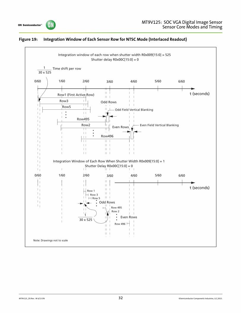
If the value in this register exceeds the maximum value given by this equation, the sensor may not generate an image. Again, the overhead time shown in this equation is only valid for the default PIXCLK_PERIOD, and the default sample (R0x7E:0) and reset (R0x87:0) valuesFigure 19 on page 32, illustrates the integration time for each sensor row versus the shutter width. Odd rows are integrated first followed by even rows.
max shutter delay Row Time Shutter Overhead–=
Row Time (R0x004 HBLANK_REG) PIXCLK_PERIOD+=
Shutter Overhead (NTSC) 356 master clock periods=
Shutter Overhead (PAL) 368 master clock periods=
NTSC max shutter delay (858 2) 356– 1360 master clock periods= =
PAL max shutter delay (864 2) 368– 1360 master clock periods= =
MT9V125_DS Rev.. W 6/15 EN 31 ©Semiconductor Components Industries, LLC,2015.
MT9V125: SOC VGA Digital Image SensorSensor Core Modes and Timing
Figure 19: Integration Window of Each Sensor Row for NTSC Mode (Interlaced Readout)
t (seconds)
0/60 1/60 2/60 3/60 4/60 5/60 6/60
. . .
. . .
1 30 x 525
Time shift per row
Integration window of each row when shutter width R0x009[15:0] = 525 Shutter delay R0x00C[15:0] = 0
t (seconds)
0/60 1/60 3/60 4/60 5/60 6/60
Odd Rows
Even Rows
. . .
. . .
Integration Window of Each Row When Shutter Width R0x009[15:0] = 1Shutter Delay R0x00C[15:0] = 0
Note: Drawings not to scale
1 30 x 525
Row 1
Row 496
Row 2 Row 495
Row 3 Row 5
Odd Rows
Even Field Vertical Blanking
2/60
Row1 (First Active Row)
Row3
Row5
Row495
Row2
Even Rows
Odd Field Vertical Blanking
Row496
MT9V125_DS Rev.. W 6/15 EN 32 ©Semiconductor Components Industries, LLC,2015.
MT9V125: SOC VGA Digital Image SensorModes and Timing
Modes and TimingThis section provides an overview of the typical usage modes and related timing infor-mation for the MT9V125.
Composite Video Output
The analog composite video output is enabled by default and is the main usage mode for the MT9V125.
The external pin NTSC_PAL_SELECT can be used to configure the device for default NTSC or PAL operation. This and other video configuration settings are available as register settings accessible through the serial interface. For proper NTSC and PAL opera-tion, use only default register values.
NTSC
Both differential and single-ended connections of the full NTSC format are supported. The differential connection that uses two output lines is used for low noise or long distance applications. The single-ended connection is used for PCB tracks and screened cable where noise is not a concern. The NTSC format has three black lines at the bottom of each image for padding (which most LCDs do not display).
PAL
The PAL format is supported with 480 active image rows only. Black bars are padded on top and bottom of the image for PAL format support. The PAL format has 24 black lines at the top and bottom of each image for padding.
NTSC or PAL with External Image Processing
The on-chip video encoder and DAC can be used with external data stream input (DIN[7:0] port). Correct NTSC or PAL formatted CCIR656 data is required for correct composite video output.
This mode can typically be used together with data output on the parallel DOUT[7:0] port—for example, for external overlay solutions.
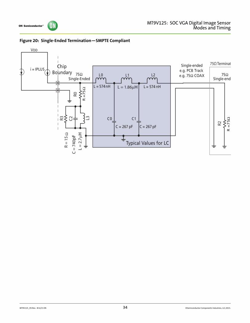
Single-Ended and Differential Composite Output
The composite output can be operated in a single-ended or differential mode by simply changing the external resistor configuration. For single-ended termination, two sche-matics are presented. The first is SMPTE-compliant; the second is a low-cost alternative.
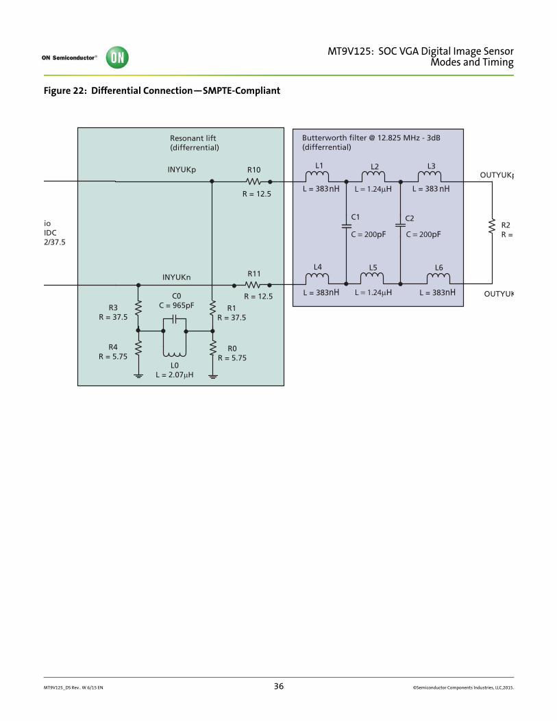
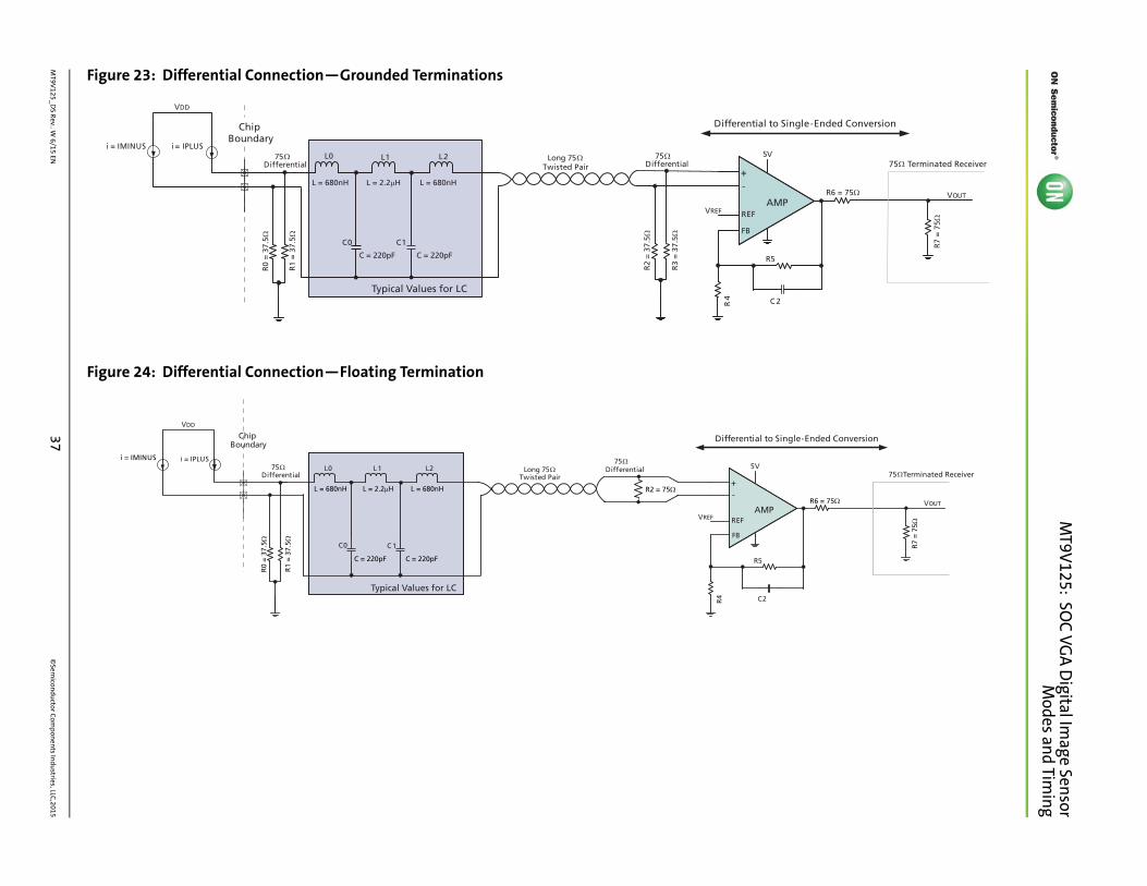
For differential mode termination, the first differential schematic; Figure 22 on page 36, is SMPTE-compliant. The other two are lost-cost alternatives.
See Figure 20 on page 34 through Figure 24 on page 37 for termination schematics.
Note: The differential schematics have not been tested.
MT9V125_DS Rev.. W 6/15 EN 33 ©Semiconductor Components Industries, LLC,2015.
MT9V125: SOC VGA Digital Image SensorModes and Timing
Figure 20: Single-Ended Termination—SMPTE Compliant
V DD
75 Ω 75 Ω
Chip Boundary
i = IPLUS
Single - Ended
R =
7 5
Ω
R =
7 5 Ω
Single-ended e . g . PCB Track e . g . 75 Ω COAX
Single - end
L = 574 nH L = 574
C = 267
C 0 C 1
C = 267
L 0 L 1 L 2
Typical Values for LC
75Ω TerminatR
= 1
5
C =
740
pF
L =
2.7
μHR
0
R2
R3
C2 L3
Ω
nH
pF pF
L = 1.86μH
MT9V125_DS Rev.. W 6/15 EN 34 ©Semiconductor Components Industries, LLC,2015.
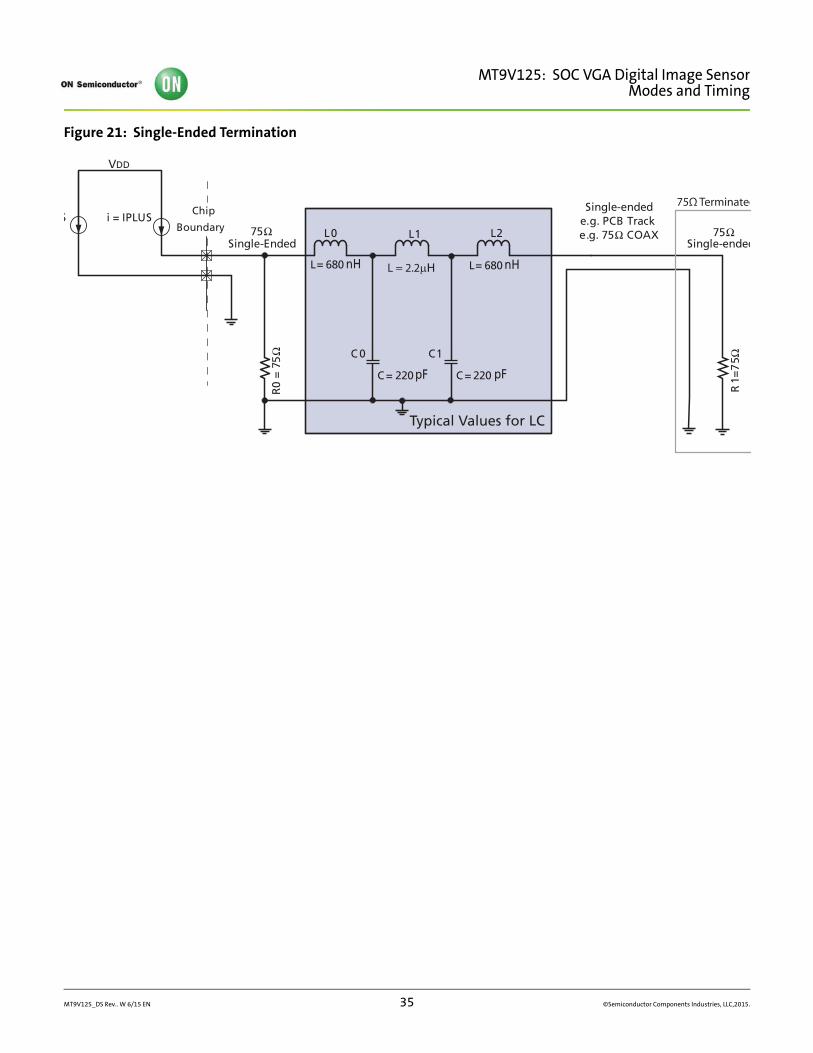
MT9V125: SOC VGA Digital Image SensorModes and Timing
Figure 21: Single-Ended Termination
VDD
75 Ω 75 Ω
Chip
Boundaryi = IPLUS S
Single - Ended
R0
= 7
5 Ω
R 1
= 7
5 Ω
Single-ended e . g . PCB Track e . g . 75 Ω COAX
Single - ended
L = 680 L = 680
C = 220
C 0 C 1
C = 220
L 0 L 1 L 2
Typical Values for LC
75Ω Terminated
nHnH L = 2.2μH
pFpF
MT9V125_DS Rev.. W 6/15 EN 35 ©Semiconductor Components Industries, LLC,2015.
MT9V125: SOC VGA Digital Image SensorModes and Timing
Figure 22: Differential Connection—SMPTE-Compliant
L = 383
C2
L1 L2 L3
L = 383
C1
L = 383nH L = 383nH
L4 L5 L6
R2 R =
OUTYUK
OUTYUKpR10
R11
R = 12.5
R = 12.5
Butterworth filter @ 12.825 MHz - 3dB (differrential)
INYUKp
INYUKn
C0C = 965pF
L0L = 2.07μH
R3 R = 37.5
R4 R = 5.75
R1 R = 37.5
R0 R = 5.75
io IDC 2/37.5
Resonant lift (differrential)
nHnH L = 1.24μH
L = 1.24μH
C = 200pFC = 200pF
MT9V125_DS Rev.. W 6/15 EN 36 ©Semiconductor Components Industries, LLC,2015.
MT9V
125_DS Rev.. W
6/15 EN37
©Sem
icondu
ctor Com
ponen
ts Indu
stries, LLC,2015
MT9V
125: SOC VG
A D
igital Image Sensor
Modes
andTim
ingFigure 23: Differential Connection—Grounded Terminations
V DD
V OUT
ed Conversion
Ω 75 Terminated Receiver
R7
= 7
5Ω
6 = 75Ω
V OUT
Conversion
75 Terminated Receiver Ω
5Ω
R7
= 7
5Ω
Figure 24: Differential Connection—Floating Termination
Long 75 Ω Twisted Pair
75 Ω 75 Ω
Chip Boundary
i = IPLUS i = IMINUS
Differential Differential
L = 2.2μHL = 680nH L = 680nH
C = 220pF C = 220pF
C 0 C 1
L 0 L 1 L 2
R 4
R5
C 2
5 V
AMP V REF
+ -
REF
FB
Differential to Single - End
Typical Values for LC
R0
= 3
7.5Ω
R1
= 3
7.5Ω
R2
= 3
7.5Ω
R3
= 3
7.5Ω
R
V DD
Long 75 Ω Twisted Pair
75 Ω 75 Ω
Chip Boundary
i = IPLUS
Differential Differential
C 0 C 1
L 0 L 1 L 2
R4
R5
C 2
5 V
AMP V REF
+ -
REF
FB
Differential to Single - Ended
Typical Values for LC
i = IMINUS
L = 2.2μHL = 680nH L = 680nH
C = 220pF C = 220pF
R0
= 3
7.5Ω
R1
= 3
7.5Ω
R2 = 75Ω
R6 = 7
MT9V125: SOC VGA Digital Image SensorModes and Timing
Serial (LVDS) Output
The serial high-speed output port supports the interlaced CCIR-656 data format.
The LVDS port is disabled by default, but can be enabled by the external pin LVDS_EN-ABLE. This pin must be asserted for LVDS to function. LVDS can be disabled through R29:1[13]. LVDS is also disabled when STANDBY is asserted.
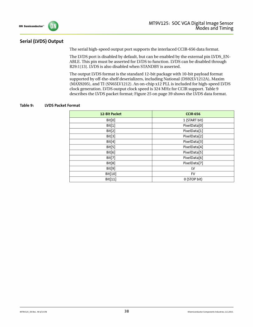
The output LVDS format is the standard 12-bit package with 10-bit payload format supported by off-the-shelf deserializers, including National (DS92LV1212A), Maxim (MAX9205), and TI (SN65LV1212). An on-chip x12 PLL is included for high-speed LVDS clock generation. LVDS output clock speed is 324 MHz for CCIR support. Table 9 describes the LVDS packet format; Figure 25 on page 39 shows the LVDS data format.
Table 9: LVDS Packet Format
12-Bit Packet CCIR-656
Bit[0] 1 (START bit)
Bit[1] PixelData[0]
Bit[2] PixelData[1]
Bit[3] PixelData[2]
Bit[4] PixelData[3]
Bit[5] PixelData[4]
Bit[6] PixelData[5]
Bit[7] PixelData[6]
Bit[8] PixelData[7]
Bit[9] LV
Bit[10] FV
Bit[11] 0 (STOP bit)
MT9V125_DS Rev.. W 6/15 EN 38 ©Semiconductor Components Industries, LLC,2015.
MT9V125: SOC VGA Digital Image SensorModes and Timing
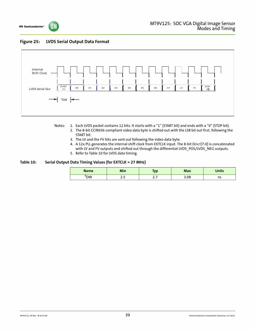
Figure 25: LVDS Serial Output Data Format
Notes: 1. Each LVDS packet contains 12 bits. It starts with a “1” (START bit) and ends with a “0” (STOP bit).2. The 8-bit CCIR656-compliant video data byte is shifted out with the LSB bit out first, following the
START bit.3. The LV and the FV bits are sent out following the video data byte.4. A 12x PLL generates the internal shift clock from EXTCLK input. The 8-bit DOUT[7:0] is concatenated
with LV and FV outputs and shifted out through the differential LVDS_POS/LVDS_NEG outputs. 5. Refer to Table 10 for LVDS data timing.
Table 10: Serial Output Data Timing Values (for EXTCLK = 27 MHz)
Name Min Typ Max UnitstDW 2.5 2.7 3.08 ns
D1D0 D3D2 D5D4 D7D6 LV FV
InternalShift Clock
LVDS Serial OutSTART
(1)STOP
(0))
tDW
MT9V125_DS Rev.. W 6/15 EN 39 ©Semiconductor Components Industries, LLC,2015.
MT9V125: SOC VGA Digital Image SensorModes and Timing
Parallel Output (DOUT)
Interlaced
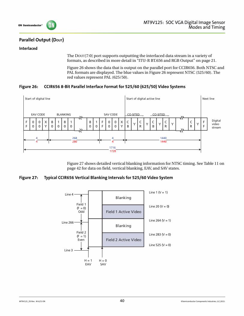
The DOUT[7:0] port supports outputting the interlaced data stream in a variety of formats, as described in more detail in “ITU-R BT.656 and RGB Output” on page 21.
Figure 26 shows the data that is output on the parallel port for CCIR656. Both NTSC and PAL formats are displayed. The blue values in Figure 26 represent NTSC (525/60). The red values represent PAL (625/50).
Figure 26: CCIR656 8-Bit Parallel Interface Format for 525/60 (625/50) Video Systems
Figure 27 shows detailed vertical blanking information for NTSC timing. See Table 11 on page 42 for data on field, vertical blanking, EAV, and SAV states.
Figure 27: Typical CCIR656 Vertical Blanking Intervals for 525/60 Video System
F F
0 0
0 0
X Y
8 0
1 0
8 0
1 0
8 0
1 0
F F
0 0
0 0
X Y
C B
Y C R
Y C B
Y C R
Y C R
Y F F
4 4
268 280
4 4
1440 1440
1716 1728
EAV CODE BLANKING SAV CODE CO - SITED _ CO - SITED _
Start of digital line Start of digital active line Next line
Digital video stream
Blanking
Field 1 Active Video
Blanking
Field 2 Active Video
Line 4
Line 266
Line 3
Field 1(F = 0)Odd
Field 2(F = 1)Even
EAV SAV
Line 1 (V = 1)
Line 20 (V = 0)
Line 264 (V = 1)
Line 283 (V = 0)
Line 525 (V = 0)
H = 1 H = 0
MT9V125_DS Rev.. W 6/15 EN 40 ©Semiconductor Components Industries, LLC,2015.
MT9V125: SOC VGA Digital Image SensorModes and Timing
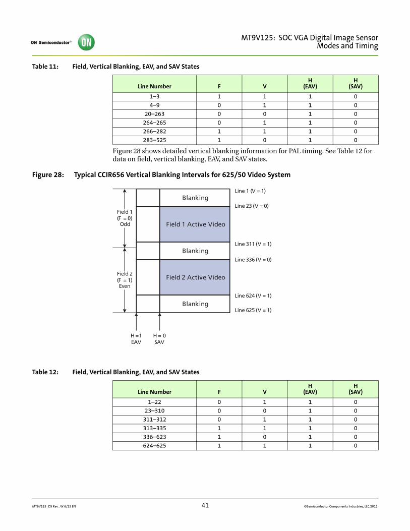
Figure 28 shows detailed vertical blanking information for PAL timing. See Table 12 for data on field, vertical blanking, EAV, and SAV states.
Figure 28: Typical CCIR656 Vertical Blanking Intervals for 625/50 Video System
Table 11: Field, Vertical Blanking, EAV, and SAV States
Line Number F VH
(EAV)H
(SAV)
1–3 1 1 1 0
4–9 0 1 1 0
20–263 0 0 1 0
264–265 0 1 1 0
266–282 1 1 1 0
283–525 1 0 1 0
Table 12: Field, Vertical Blanking, EAV, and SAV States
Line Number F VH
(EAV)H
(SAV)
1–22 0 1 1 0
23–310 0 0 1 0
311–312 0 1 1 0
313–335 1 1 1 0
336–623 1 0 1 0
624–625 1 1 1 0
Blanking
Field 1 Active Video
Blanking
Field 2 Active Video
Field 1(F = 0)Odd
Field 2(F = 1)Even
H = 1EAV
H = 0SAV
Blanking
Line 1 (V = 1)
Line 23 (V = 0)
Line 311 (V = 1)
Line 336 (V = 0)
Line 625 (V = 1)
Line 624 (V = 1)
MT9V125_DS Rev.. W 6/15 EN 41 ©Semiconductor Components Industries, LLC,2015.
MT9V125: SOC VGA Digital Image SensorModes and Timing
Progressive
The DOUT[7:0] port also supports progressive, raw data output. The on-chip color processor does not support reading out the pixel array progressively, but the raw pixel data can be made available in sensor stand-alone mode.
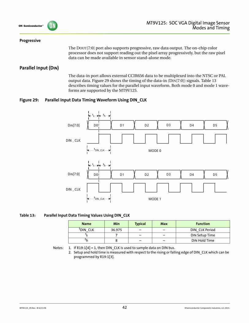
Parallel Input (DIN)
The data-in port allows external CCIR656 data to be multiplexed into the NTSC or PAL output data. Figure 29 shows the timing of the data-in (DIN[7:0]) signals. Table 13 describes timing values for the parallel input waveform. Both mode 0 and mode 1 wave-forms are supported by the MT9V125.
Figure 29: Parallel Input Data Timing Waveform Using DIN_CLK
Notes: 1. If R19:1[4] = 1, then DIN_CLK is used to sample data on DIN bus.2. Setup and hold time is measured with respect to the rising or falling edge of DIN_CLK which can be
programmed by R19:1[3].
Table 13: Parallel Input Data Timing Values Using DIN_CLK
Name Min Typical Max FunctiontDIN_CLK 36.975 – – DIN_CLK Period
ts 7 – – DIN Setup Timeth 8 – – DIN Hold Time
tDIN_CLK
ts th
D 0 D 1 D 2 D 3 D 4 D 5 DIN[7:0]
MODE 0
tDIN_ CLK
ts th
D 0 D 1 D 2 D 3 D 4 D 5
DIN _ CLK
MODE 1
DIN _ CLK
DIN[7:0]
MT9V125_DS Rev.. W 6/15 EN 42 ©Semiconductor Components Industries, LLC,2015.
MT9V125: SOC VGA Digital Image SensorModes and Timing
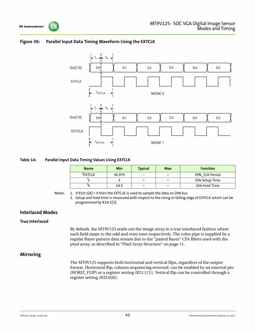
Figure 30: Parallel Input Data Timing Waveform Using the EXTCLK
Notes: 1. If R19:1[4] = 0 then the EXTCLK is used to sample the data on DIN bus.2. Setup and hold time is measured with respect to the rising or falling edge of EXTCLK which can be
programmed by R19:1[3].
Interlaced Modes
True Interlaced
By default, the MT9V125 reads out the image array in a true interlaced fashion where each field maps to the odd and even rows respectively. The color pipe is supplied by a regular Bayer pattern data stream due to the “paired Bayer” CFA filters used with the pixel array, as described in “Pixel Array Structure” on page 11.
Mirroring
The MT9V125 supports both horizontal and vertical flips, regardless of the output format. Horizontal flip, column sequencing reversed, can be enabled by an external pin (HORIZ_FLIP) or a register setting (R21:1[1]). Vertical flip can be controlled through a register setting (R32:0[0]).
Table 14: Parallel Input Data Timing Values Using EXTCLK
Name Min Typical Max FunctiontEXTCLK 36.975 – – DIN_CLK Period
ts 3 – – DIN Setup Timeth 14.5 – – DIN Hold Time
ts th
D 0 D 1 D 2 D 3 D 4 D 5 DIN[7:0]
MODE 0
ts th
D 0 D 1 D 2 D 3 D 4 D 5
MODE 1
DIN[7:0]
EXTCLK
EXTCLK
tEXTCLK
tEXTCLK
MT9V125_DS Rev.. W 6/15 EN 43 ©Semiconductor Components Industries, LLC,2015.
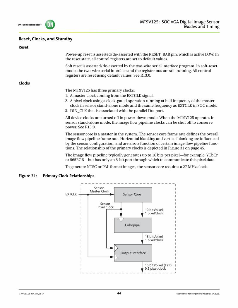
MT9V125: SOC VGA Digital Image SensorModes and Timing
Reset, Clocks, and Standby
Reset
Power-up reset is asserted/de-asserted with the RESET_BAR pin, which is active LOW. In the reset state, all control registers are set to default values.
Soft reset is asserted/de-asserted by the two-wire serial interface program. In soft-reset mode, the two-wire serial interface and the register bus are still running. All control registers are reset using default values. See R13:0.
Clocks
The MT9V125 has three primary clocks:1. A master clock coming from the EXTCLK signal.2. A pixel clock using a clock-gated operation running at half frequency of the master
clock in sensor stand-alone mode and the same frequency as EXTCLK in SOC mode. 3. DIN_CLK that is associated with the parallel DIN port.
All device clocks are turned off in power-down mode. When the MT9V125 operates in sensor stand-alone mode, the image flow pipeline clocks can be shut off to conserve power. See R13:0.
The sensor core is a master in the system. The sensor core frame rate defines the overall image flow pipeline frame rate. Horizontal blanking and vertical blanking are influenced by the sensor configuration, and are also a function of certain image flow pipeline func-tions. The relationship of the primary clocks is depicted in Figure 31 on page 45.
The image flow pipeline typically generates up to 16 bits per pixel—for example, YCbCr or 565RGB—but has only an 8-bit port through which to communicate this pixel data.
To generate NTSC or PAL format images, the sensor core requires a 27 MHz clock.
Figure 31: Primary Clock Relationships
10 bits/pixel1 pixel/clock
16 bits/pixel1 pixel/clock
16 bits/pixel (TYP)0.5 pixel/clock
Colorpipe
Output Interface
Sensor Pixel Clock
Sensor Master Clock
EXTCLK Sensor Core
MT9V125_DS Rev.. W 6/15 EN 44 ©Semiconductor Components Industries, LLC,2015.
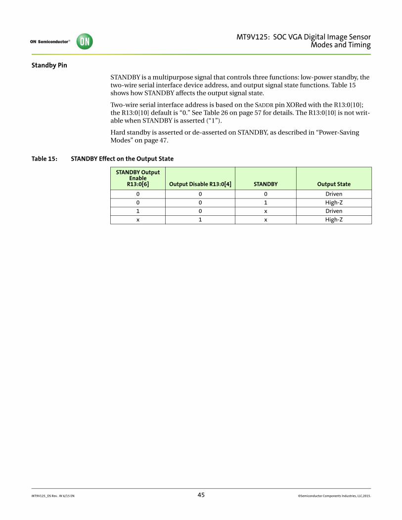
MT9V125: SOC VGA Digital Image SensorModes and Timing
Standby Pin
STANDBY is a multipurpose signal that controls three functions: low-power standby, the two-wire serial interface device address, and output signal state functions. Table 15 shows how STANDBY affects the output signal state.
Two-wire serial interface address is based on the SADDR pin XORed with the R13:0[10]; the R13:0[10] default is “0.” See Table 26 on page 57 for details. The R13:0[10] is not writ-able when STANDBY is asserted (“1”).
Hard standby is asserted or de-asserted on STANDBY, as described in “Power-Saving Modes” on page 47.
Table 15: STANDBY Effect on the Output State
STANDBY Output Enable
R13:0[6] Output Disable R13:0[4] STANDBY Output State
0 0 0 Driven
0 0 1 High-Z
1 0 x Driven
x 1 x High-Z
MT9V125_DS Rev.. W 6/15 EN 45 ©Semiconductor Components Industries, LLC,2015.
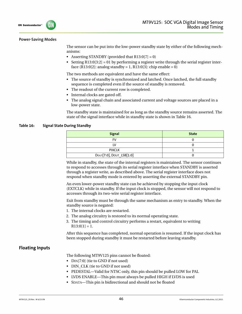
MT9V125: SOC VGA Digital Image SensorModes and Timing
Power-Saving Modes
The sensor can be put into the low-power standby state by either of the following mech-anisms:• Asserting STANDBY (provided that R13:0[7] = 0)• Setting R13:0[3:2] = 01 by performing a register write through the serial register inter-
face (R13:0[2]: analog standby = 1, R13:0[3]: chip enable = 0)
The two methods are equivalent and have the same effect:• The source of standby is synchronized and latched. Once latched, the full standby
sequence is completed even if the source of standby is removed.• The readout of the current row is completed.• Internal clocks are gated off.• The analog signal chain and associated current and voltage sources are placed in a
low-power state.
The standby state is maintained for as long as the standby source remains asserted. The state of the signal interface while in standby state is shown in Table 16.
While in standby, the state of the internal registers is maintained. The sensor continues to respond to accesses through its serial register interface when STANDBY is asserted through a register write, as described above. The serial register interface does not respond when standby mode is entered by asserting the external STANDBY pin.
An even lower-power standby state can be achieved by stopping the input clock (EXTCLK) while in standby. If the input clock is stopped, the sensor will not respond to accesses through its two-wire serial register interface.
Exit from standby must be through the same mechanism as entry to standby. When the standby source is negated:1. The internal clocks are restarted.2. The analog circuitry is restored to its normal operating state.3. The timing and control circuitry performs a restart, equivalent to writing
R13:0[1] = 1.
After this sequence has completed, normal operation is resumed. If the input clock has been stopped during standby it must be restarted before leaving standby.
Floating Inputs
The following MT9V125 pins cannot be floated:• DIN[7:0] (tie to GND if not used)• DIN_CLK (tie to GND if not used)• PEDESTAL—Valid for NTSC only, this pin should be pulled LOW for PAL• LVDS ENABLE—This pin must always be pulled HIGH if LVDS is used• SDATA—This pin is bidirectional and should not be floated
Table 16: Signal State During Standby
Signal State
FV 0
LV 0
PIXCLK 1
DOUT[7:0], DOUT_LSB[1:0] 0
MT9V125_DS Rev.. W 6/15 EN 46 ©Semiconductor Components Industries, LLC,2015.

MT9V125: SOC VGA Digital Image SensorModes and Timing
Output Data Ordering
Notes: 1. PIXCLK is 27 MHz when EXTCLK is 27 MHz.
Notes: 1. PIXCLK is 13.5 MHz when EXTCLK is 27 MHz.
Notes: 1. Data output rate is 324 Mb/s when EXTCLK is 27 MHz.
Table 17: Output Data Ordering in DOUT RGB Mode
Mode(Swap Disabled) Byte D7 D6 D5 D4 D3 D2 D1 D0
565RGB First R7 R6 R5 R4 R3 G7 G6 G5
Second G4 G3 G2 B7 B6 B5 B4 B3
555RGB First 0 R7 R6 R5 R4 R3 G7 G6
Second G5 G4 G3 B7 B6 B5 B4 B3
444xRGB First R7 R6 R5 R4 G7 G6 G5 G4
Second B7 B6 B5 B4 0 0 0 0
x444RGB First 0 0 0 0 R7 R6 R5 R4
Second G7 G6 G5 G4 B7 B6 B5 B4
Table 18: Output Data Ordering in Sensor Stand-Alone Mode
Mode D7 D6 D5 D4 D3 D2 D1 D0 DOUT_LSB1 DOUT_LSB0
10-bit Output B9 B8 B7 B6 B5 B4 B3 B2 B1 B0
Table 19: Data Ordering in LVDS Serial Mode
Mode Package[0] Package[8:1] Package[9] Package[10] Package[11]
Default Start bit “1’ DOUT[7:0] LINE_VALID FRAME_VALID Stop bit “0”
MT9V125_DS Rev.. W 6/15 EN 47 ©Semiconductor Components Industries, LLC,2015.

MT9V125: SOC VGA Digital Image SensorModes and Timing
I/O Circuitry
Figure 32 and Figure 33 on page 50 illustrate typical circuitry used for each input, output or I/O pad.
Figure 32: Typical I/O Equivalent Circuits
Notes: 1. All I/O circuitry shown above is for reference only. The actual implementation may be different.
VDD
Pad
Input Pad
Receiver
VDD
Pad
Output Pad
TriStateDriver
GND
GND VDD
GND
Receiver
TriStateDriver
VDD GNDPad
VDD
GND
GND
I/O Pad
SDATA
FRAME_VALIDLINE_VALID
DOUT_LSB[1:0]DOUT[7:0]
PIXCLK
DIN[7:0]DIN_CLK
SCLKLVDS_ENABLE
STANDBYPEDESTAL
NTSC_PAL_SELECTHORIZ_FLIP
MT9V125_DS Rev.. W 6/15 EN 48 ©Semiconductor Components Industries, LLC,2015.
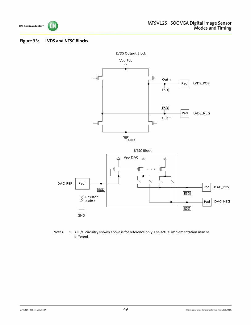
MT9V125: SOC VGA Digital Image SensorModes and Timing
Figure 33: LVDS and NTSC Blocks
Notes: 1. All I/O circuitry shown above is for reference only. The actual implementation may be different.
VDD_PLL
GND
Pad
VDD_DAC
GND
Pad
Pad
ESD
ESD
Out +
Out
LVDS Output Block
Pad
Pad
ESDESD
DAC_REF
ESD
DAC_POS
DAC_NEG
NTSC Block
Resistor2.8kΩ
LVDS_POS
LVDS_NEG
MT9V125_DS Rev.. W 6/15 EN 49 ©Semiconductor Components Industries, LLC,2015.
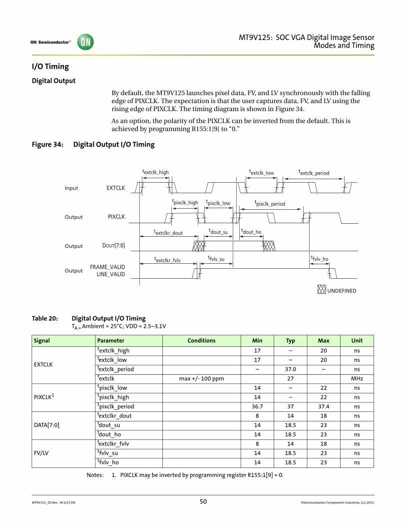
MT9V125: SOC VGA Digital Image SensorModes and Timing
I/O Timing
Digital Output
By default, the MT9V125 launches pixel data, FV, and LV synchronously with the falling edge of PIXCLK. The expectation is that the user captures data, FV, and LV using the rising edge of PIXCLK. The timing diagram is shown in Figure 34.
As an option, the polarity of the PIXCLK can be inverted from the default. This is achieved by programming R155:1[9] to “0.”
Figure 34: Digital Output I/O Timing
Notes: 1. PIXCLK may be inverted by programming register R155:1[9] = 0.
Table 20: Digital Output I/O Timing TA = Ambient = 25°C; VDD = 2.5–3.1V
Signal Parameter Conditions Min Typ Max Unit
EXTCLK
textclk_high 17 – 20 nstextclk_low 17 – 20 nstextclk_period – 37.0 – nsfextclk max +/- 100 ppm 27 MHz
PIXCLK1
tpixclk_low 14 – 22 nstpixclk_high 14 – 22 nstpixclk_period 36.7 37 37.4 ns
DATA[7:0]
textclkr_dout 8 14 18 nstdout_su 14 18.5 23 nstdout_ho 14 18.5 23 ns
FV/LV
textclkr_fvlv 8 14 18 nstfvlv_su 14 18.5 23 nstfvlv_ho 14 18.5 23 ns
tdout_su tdout_ho
EXTCLK
PIXCLK
DOUT[7:0]
FRAME_VALIDLINE_VALID
tpixclk_lowtpixclk_high
textclk_high
tfvlv_su tfvlv_ho
textclkr_dout
textclkr_fvlv
textclk_low
UNDEFINED
Input
Output
Output
Output
textclk_period
tpixclk_period
MT9V125_DS Rev.. W 6/15 EN 50 ©Semiconductor Components Industries, LLC,2015.
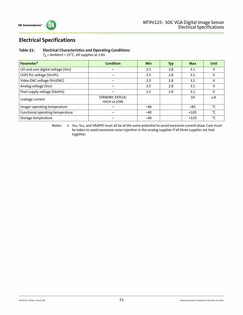
MT9V125: SOC VGA Digital Image SensorElectrical Specifications
Electrical Specifications
Notes: 1. VDD, VAA, and VAAPIX must all be at the same potential to avoid excessive current draw. Care must be taken to avoid excessive noise injection in the analog supplies if all three supplies are tied together.
Table 21: Electrical Characteristics and Operating ConditionsTA = Ambient = 25°C; All supplies at 2.8V
Parameter1 Condition Min Typ Max Unit
I/O and core digital voltage (VDD) – 2.5 2.8 3.1 V
LVDS PLL voltage (VDDPLL – 2.5 2.8 3.1 V
Video DAC voltage (VDDDAC) – 2.5 2.8 3.1 V
Analog voltage (VAA) – 2.5 2.8 3.1 V
Pixel supply voltage (VAAPIX) – 2.5 2.8 3.1 V
Leakage current STANDBY, EXTCLK:HIGH or LOW
10 A
Imager operating temperature – –40 +85 °C
Functional operating temperature – –40 +105 °C
Storage temperature – –40 +125 °C
MT9V125_DS Rev.. W 6/15 EN 51 ©Semiconductor Components Industries, LLC,2015.
MT9V125: SOC VGA Digital Image SensorElectrical Specifications
Notes: 1. RDAC_REF = 2.8k
Table 22: Video DAC Electrical CharacteristicsTA = Ambient = 25°C; All supplies at 2.8V
Parameter Condition Min Typ Max Unit
Resolution – 10 – bits
DNL Single-ended mode – 0.8 1.1 bits
INL Single-ended mode – 5.7 8.1 bits
Output local loadSingle-ended mode, output pad (DAC_POS) – 75 –
Single-ended mode, unused output (DAC_NEG) – 0 –
Output voltageSingle-ended mode, code 000h – 0.02 – V
Single-ended mode, code 3FFh – 1.42 – V
Output currentSingle-ended mode, code 000h – 0.6 – mA
Single-ended mode, code 3FFh – 37.9 – mA
DNL Differential mode – 0.7 1 bits
INL Differential mode – 1.4 3 bits
Output local loadDifferential mode per pad(DAC_POS and DAC_NEG)
– 37.5 –
Output voltage
Differential mode, code 000h, pad dacp – 0.37 – V
Differential mode, code 000h, pad dacn – 1.07 – V
Differential mode, code 3FFh, pad dacp – 1.07 – V
Differential mode, code 3FFH, pad dacn – 0.37 – V
Output voltage
Differential mode, code 000h, pad dacp – 0.6 – mA
Differential mode, code 000h, pad dacn – 37.9 – mA
Differential mode, code 3FFh, pad dacp – 37.9 – mA
Differential mode, code 3FFH, pad dacn – 0.6 – mA
Differential output, mid level
Differential mode– 0.72 – V
Supply current Estimate – – 55 mA
DAC_REF1 DAC Reference – 1.15 +/–0.2 V
MT9V125_DS Rev.. W 6/15 EN 52 ©Semiconductor Components Industries, LLC,2015.

MT9V125: SOC VGA Digital Image SensorElectrical Specifications
Power Consumption
Notes: 1. 10pF nominal.2. (NTSC or PAL) and LVDS should not be operated at the same time.
Table 23: Digital I/O ParametersTA = Ambient = 25°C; All supplies at 2.8V
Signal Parameter Definitions Condition Min Typ Max Unit
All Outputs
Load capacitance 1 – 30 pF
Output signal slew2.8V, 30pF load – 0.72 – V/ns
2.8V, 5pF load – 1.25 – V/ns
VOH Output high voltage 2.5 2.8 3.1 V
VOL Output low voltage –0.3 – 0.3 V
IOH Output high current VDD = 2.8V, VOH = 2.4V 16 – 26.5 mA
IOL Output low current VDD = 2.8V, VOL = 0.4V 15.9 – 21.3 mA
All Inputs
VIH Input high voltage VDD = 2.8V 1.48 – VDD + 0.3
V
VIL Input low voltage VDD = 2.8V – – 1.43 V
IIN Input leakage current –2 – 2 A
Signal CAP Input signal capacitance – 3.5 – pF
Table 24: Power ConsumptionTA = Ambient = 25°C; All supplies at 2.8V
ModeSensor(mW)
Image-Flow Proc(mW)
I/Os (mW)1
DAC(mW) LVDS (mW)
Total (mW)
Active mode 2 60 100 10 150 80 400
Standby 0.56
MT9V125_DS Rev.. W 6/15 EN 53 ©Semiconductor Components Industries, LLC,2015.
MT9V125: SOC VGA Digital Image SensorElectrical Specifications
NTSC Signal Parameters
Notes: 1. Black and white levels are referenced to the blanking level.2. NTSC convention standardized by the IRE (1 IRE = 7.14mV).3. Encoder contrast setting R0x011 = R0x001 = 0.4. DAC ref = 2.8kload = 37.5
Table 25: NTSC Signal ParametersTA = Ambient = 25°C; All supplies at 2.8V
Parameter Conditions Min Typ Max Units Notes
Line Frequency 15730 15735 15740 Hz
Field Frequency 59.00 59.94 60.00 Hz
Sync Rise Time 120 164 170 ns
Sync Fall Time 120 167 170 ns
Sync Width 4.60 4.74 4.80 s
Sync Level 37 39.9 43 IRE 2, 4
Burst Level 37 39.7 43 IRE 2, 4
Sync to Setup (with pedestal off)
9.10 9.40 9.40 s
Sync to Burst Start 5.00 5.31 5.60 s
Front Porch 1.40 1.40 1.60 s
Burst Width 8.0 8.5 10.0 cycles
Black Level 6.5 7.5 8.5 IRE 1, 2, 4
White Level 90 100 110 IRE 1, 2, 3, 4
MT9V125_DS Rev.. W 6/15 EN 54 ©Semiconductor Components Industries, LLC,2015.
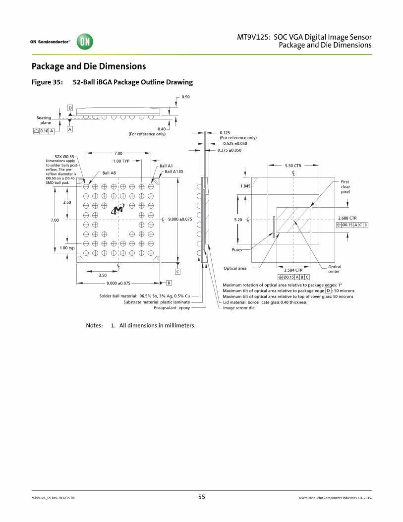
MT9V125: SOC VGA Digital Image SensorPackage and Die Dimensions
Package and Die Dimensions
Figure 35: 52-Ball iBGA Package Outline Drawing
Notes: 1. All dimensions in millimeters.
Seatingplane
9.000 ±0.075
3.50
3.50
Encapsulant: epoxy Image sensor dieLid material: borosilicate glass 0.40 thickness
Optical area
Fuses
0.40 (For reference only)
0.90
5.50 CTR
7.00
5.20
1.845
1.00 TYP
9.000 ±0.075
0.375 ±0.050
0.525 ±0.050
0.125 (For reference only)
C L C L
C L
C L
7.00
Substrate material: plastic laminate
Solder ball material: 96.5% Sn, 3% Ag, 0.5% Cu
Maximum rotation of optical area relative to package edges: 1º
0.10 A A
D
Ball A1 IDBall A1
Ball A8
52X Ø0.55Dimensions applyto solder balls post-reflow. The pre-reflow diameter isØ0.50 on a Ø0.40SMD ball pad.
1.00 typ
Firstclearpixel
Maximum tilt of optical area relative to package edge : 50 micronsMaximum tilt of optical area relative to top of cover glass: 50 microns
D
3.584 CTR
2.688 CTR
Ø0.15 A B C
Ø0.15 A BC
OpticalcenterC
B
MT9V125_DS Rev.. W 6/15 EN 55 ©Semiconductor Components Industries, LLC,2015.
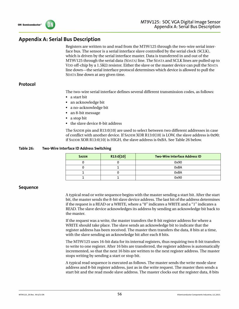
MT9V125: SOC VGA Digital Image SensorAppendix A: Serial Bus Description
Appendix A: Serial Bus DescriptionRegisters are written to and read from the MT9V125 through the two-wire serial inter-face bus. The sensor is a serial interface slave controlled by the serial clock (SCLK), which is driven by the serial interface master. Data is transferred in and out of the MT9V125 through the serial data (SDATA) line. The SDATA and SCLK lines are pulled up to VDD off-chip by a 1.5K resistor. Either the slave or the master device can pull the SDATA line down—the serial interface protocol determines which device is allowed to pull the SDATA line down at any given time.
Protocol
The two-wire serial interface defines several different transmission codes, as follows:• a start bit• an acknowledge bit• a no-acknowledge bit• an 8-bit message• a stop bit• the slave device 8-bit address
The SADDR pin and R13:0[10] are used to select between two different addresses in case of conflict with another device. If SADDR XOR R13:0[10] is LOW, the slave address is 0x90; if SADDR XOR R13:0[10] is HIGH, the slave address is 0xBA. See Table 26 below.
Sequence
A typical read or write sequence begins with the master sending a start bit. After the start bit, the master sends the 8-bit slave device address. The last bit of the address determines if the request is a READ or a WRITE, where a “0” indicates a WRITE and a “1” indicates a READ. The slave device acknowledges its address by sending an acknowledge bit back to the master.
If the request was a write, the master transfers the 8-bit register address for where a WRITE should take place. The slave sends an acknowledge bit to indicate that the register address has been received. The master then transfers the data, 8 bits at a time, with the slave sending an acknowledge bit after each 8 bits.
The MT9V125 uses 16-bit data for its internal registers, thus requiring two 8-bit transfers to write to one register. After 16 bits are transferred, the register address is automatically incremented, so that the next 16 bits are written to the next register address. The master stops writing by sending a start or stop bit.
A typical read sequence is executed as follows. The master sends the write mode slave address and 8-bit register address, just as in the write request. The master then sends a start bit and the read mode slave address. The master clocks out the register data, 8 bits
Table 26: Two-Wire Interface ID Address Switching
SADDR R13:0[10] Two-Wire Interface Address ID
0 0 0x90
0 1 0xBA
1 0 0xBA
1 1 0x90
MT9V125_DS Rev.. W 6/15 EN 56 ©Semiconductor Components Industries, LLC,2015.
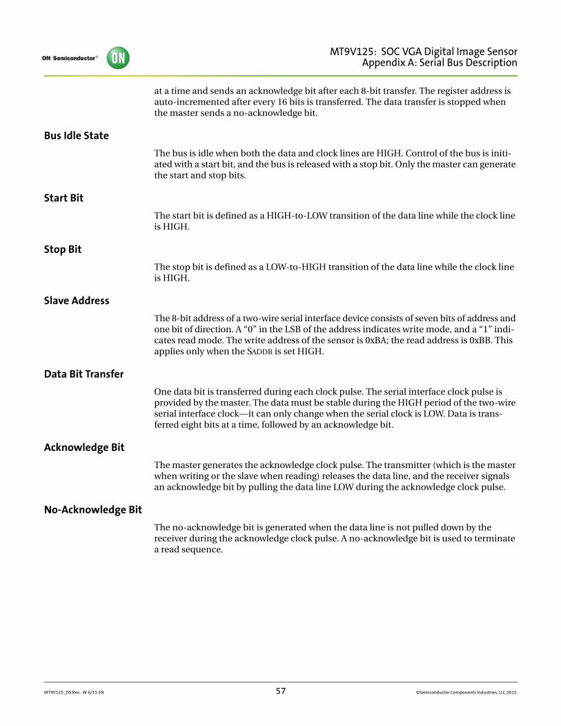
MT9V125: SOC VGA Digital Image SensorAppendix A: Serial Bus Description
at a time and sends an acknowledge bit after each 8-bit transfer. The register address is auto-incremented after every 16 bits is transferred. The data transfer is stopped when the master sends a no-acknowledge bit.
Bus Idle State
The bus is idle when both the data and clock lines are HIGH. Control of the bus is initi-ated with a start bit, and the bus is released with a stop bit. Only the master can generate the start and stop bits.
Start Bit
The start bit is defined as a HIGH-to-LOW transition of the data line while the clock line is HIGH.
Stop Bit
The stop bit is defined as a LOW-to-HIGH transition of the data line while the clock line is HIGH.
Slave Address
The 8-bit address of a two-wire serial interface device consists of seven bits of address and one bit of direction. A “0” in the LSB of the address indicates write mode, and a “1” indi-cates read mode. The write address of the sensor is 0xBA; the read address is 0xBB. This applies only when the SADDR is set HIGH.
Data Bit Transfer
One data bit is transferred during each clock pulse. The serial interface clock pulse is provided by the master. The data must be stable during the HIGH period of the two-wire serial interface clock—it can only change when the serial clock is LOW. Data is trans-ferred eight bits at a time, followed by an acknowledge bit.
Acknowledge Bit
The master generates the acknowledge clock pulse. The transmitter (which is the master when writing or the slave when reading) releases the data line, and the receiver signals an acknowledge bit by pulling the data line LOW during the acknowledge clock pulse.
No-Acknowledge Bit
The no-acknowledge bit is generated when the data line is not pulled down by the receiver during the acknowledge clock pulse. A no-acknowledge bit is used to terminate a read sequence.
MT9V125_DS Rev.. W 6/15 EN 57 ©Semiconductor Components Industries, LLC,2015.
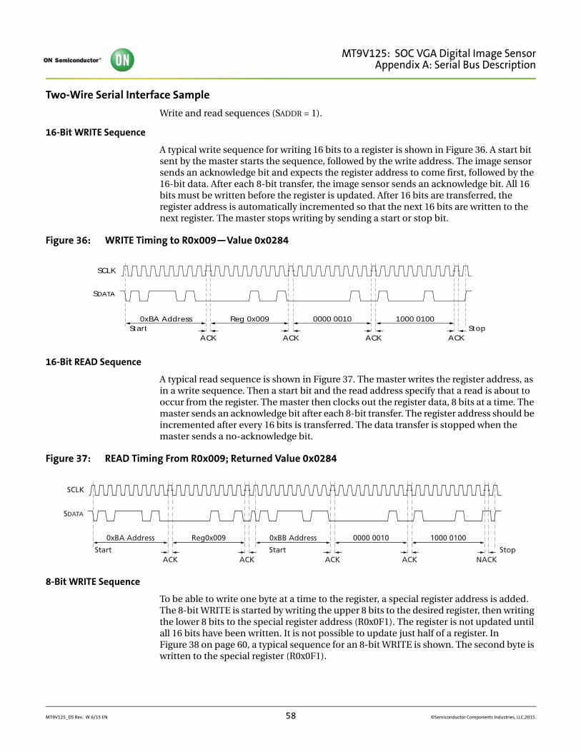
MT9V125: SOC VGA Digital Image SensorAppendix A: Serial Bus Description
Two-Wire Serial Interface Sample
Write and read sequences (SADDR = 1).
16-Bit WRITE Sequence
A typical write sequence for writing 16 bits to a register is shown in Figure 36. A start bit sent by the master starts the sequence, followed by the write address. The image sensor sends an acknowledge bit and expects the register address to come first, followed by the 16-bit data. After each 8-bit transfer, the image sensor sends an acknowledge bit. All 16 bits must be written before the register is updated. After 16 bits are transferred, the register address is automatically incremented so that the next 16 bits are written to the next register. The master stops writing by sending a start or stop bit.
Figure 36: WRITE Timing to R0x009—Value 0x0284
16-Bit READ Sequence
A typical read sequence is shown in Figure 37. The master writes the register address, as in a write sequence. Then a start bit and the read address specify that a read is about to occur from the register. The master then clocks out the register data, 8 bits at a time. The master sends an acknowledge bit after each 8-bit transfer. The register address should be incremented after every 16 bits is transferred. The data transfer is stopped when the master sends a no-acknowledge bit.
Figure 37: READ Timing From R0x009; Returned Value 0x0284
8-Bit WRITE Sequence
To be able to write one byte at a time to the register, a special register address is added. The 8-bit WRITE is started by writing the upper 8 bits to the desired register, then writing the lower 8 bits to the special register address (R0x0F1). The register is not updated until all 16 bits have been written. It is not possible to update just half of a register. In Figure 38 on page 60, a typical sequence for an 8-bit WRITE is shown. The second byte is written to the special register (R0x0F1).
SCLK
SDATA
0xBA Address Start Stop
ACK ACK ACK ACK
Reg 0x009 0000 0010 1000 0100
SCLK
SDATA
0xBA Address
Start Start StopACK ACK ACK ACK NACK
Reg0x009 0xBB Address 0000 0010 1000 0100
MT9V125_DS Rev.. W 6/15 EN 58 ©Semiconductor Components Industries, LLC,2015.
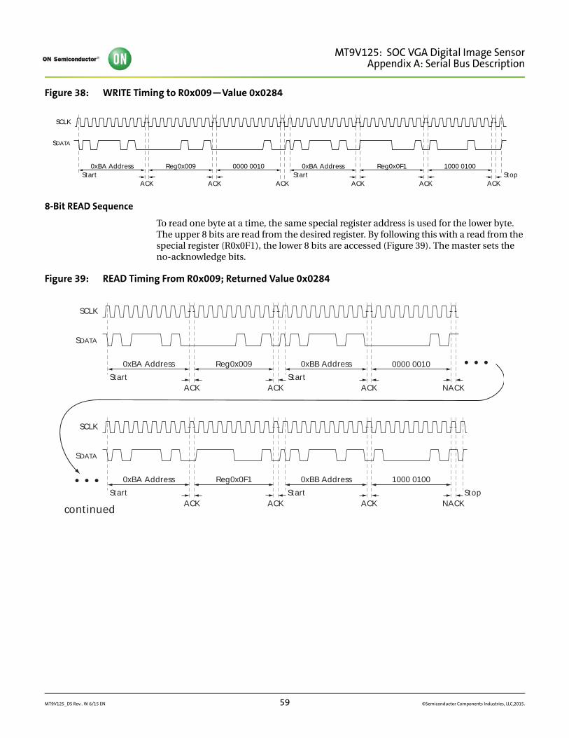
MT9V125: SOC VGA Digital Image SensorAppendix A: Serial Bus Description
Figure 38: WRITE Timing to R0x009—Value 0x0284
8-Bit READ Sequence
To read one byte at a time, the same special register address is used for the lower byte. The upper 8 bits are read from the desired register. By following this with a read from the special register (R0x0F1), the lower 8 bits are accessed (Figure 39). The master sets the no-acknowledge bits.
Figure 39: READ Timing From R0x009; Returned Value 0x0284
SCLK
SDATA
0xBA Address Start Stop
ACK ACK ACK ACK
Reg0x009 0xBA Address Start
ACK ACK
Reg0x0F10000 0010 1000 0100
SCLK
SDATA
0xBA Address
Start StartACK ACK ACK NACK
Reg0x009 0xBB Address 0000 0010
SCLK
SDATA
0xBA Address
Start Start StopACK ACK ACK NACK
Reg0x0F1 0xBB Address 1000 0100
• • •
• • •
continued
MT9V125_DS Rev.. W 6/15 EN 59 ©Semiconductor Components Industries, LLC,2015.
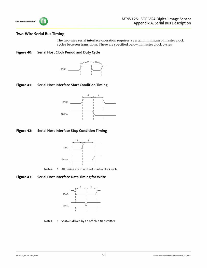
MT9V125: SOC VGA Digital Image SensorAppendix A: Serial Bus Description
Two-Wire Serial Bus Timing
The two-wire serial interface operation requires a certain minimum of master clock cycles between transitions. These are specified below in master clock cycles.
Figure 40: Serial Host Clock Period and Duty Cycle
Figure 41: Serial Host Interface Start Condition Timing
Figure 42: Serial Host Interface Stop Condition Timing
Notes: 1. All timing are in units of master clock cycle.
Figure 43: Serial Host Interface Data Timing for Write
Notes: 1. SDATA is driven by an off-chip transmitter.
SCLK
< 400 KHz Max
SCLK
4
SDATA
4
SCLK
5
SDATA
4
SCLK
4
SDATA
4
MT9V125_DS Rev.. W 6/15 EN 60 ©Semiconductor Components Industries, LLC,2015.
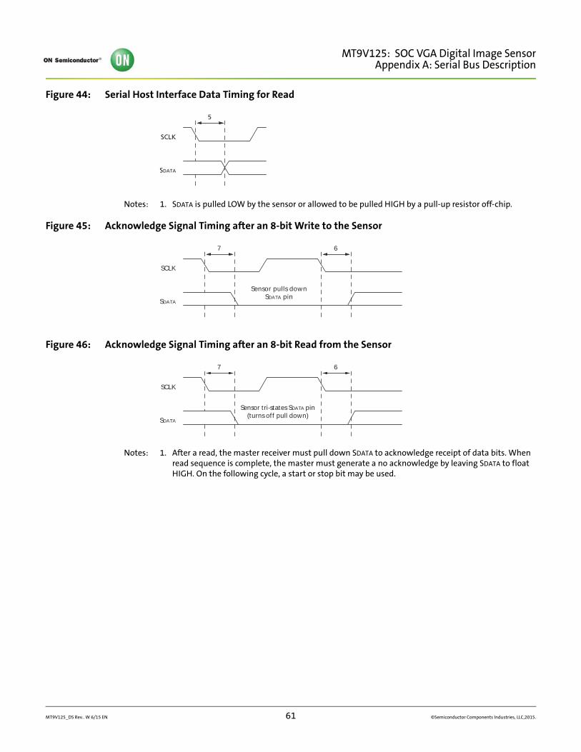
MT9V125: SOC VGA Digital Image SensorAppendix A: Serial Bus Description
Figure 44: Serial Host Interface Data Timing for Read
Notes: 1. SDATA is pulled LOW by the sensor or allowed to be pulled HIGH by a pull-up resistor off-chip.
Figure 45: Acknowledge Signal Timing after an 8-bit Write to the Sensor
Figure 46: Acknowledge Signal Timing after an 8-bit Read from the Sensor
Notes: 1. After a read, the master receiver must pull down SDATA to acknowledge receipt of data bits. When read sequence is complete, the master must generate a no acknowledge by leaving SDATA to float HIGH. On the following cycle, a start or stop bit may be used.
SCLK
5
SDATA
SCLK
Sensor pulls downSDATA pin
7
SDATA
6
SCLK
Sensor tri-states SDATA pin(turns off pull down)
7
SDATA
6
MT9V125_DS Rev.. W 6/15 EN 61 ©Semiconductor Components Industries, LLC,2015.
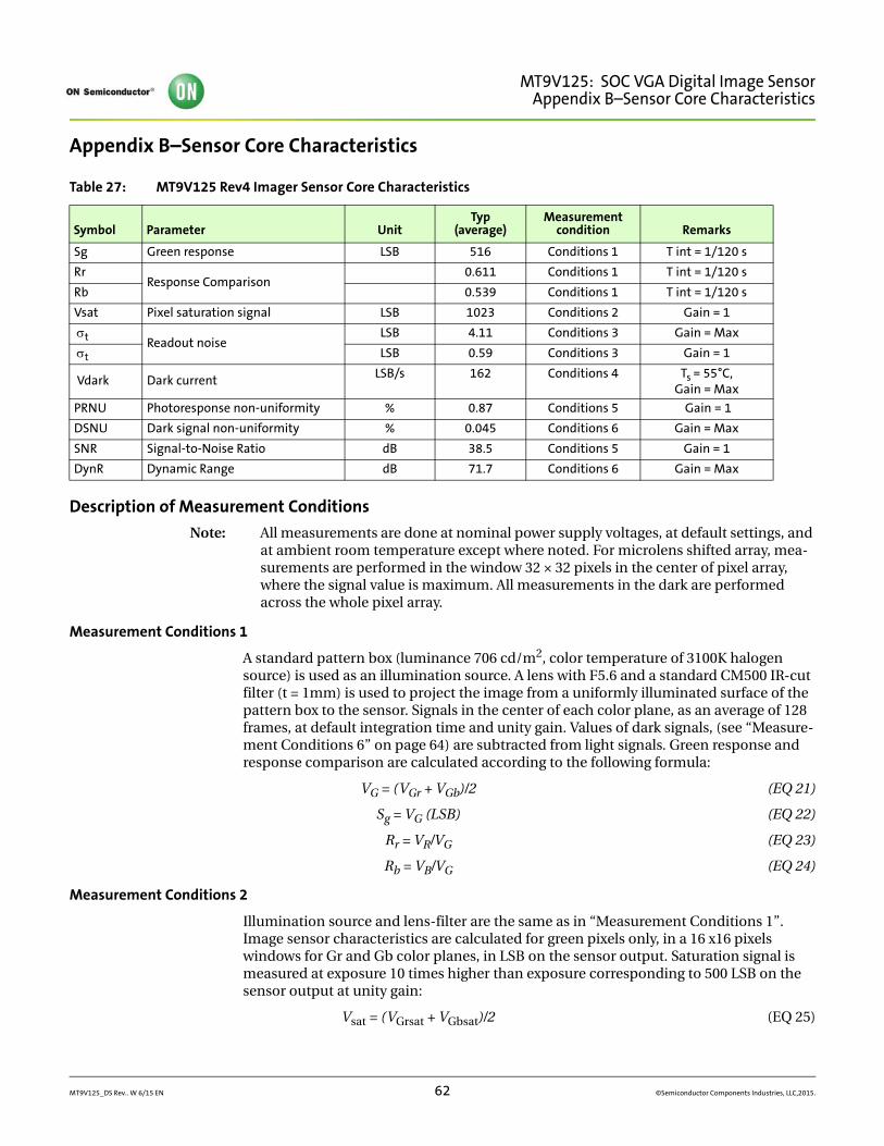
MT9V125: SOC VGA Digital Image SensorAppendix B–Sensor Core Characteristics
Appendix B–Sensor Core Characteristics
Description of Measurement Conditions
Note: All measurements are done at nominal power supply voltages, at default settings, and at ambient room temperature except where noted. For microlens shifted array, mea-surements are performed in the window 32 × 32 pixels in the center of pixel array, where the signal value is maximum. All measurements in the dark are performed across the whole pixel array.
Measurement Conditions 1
A standard pattern box (luminance 706 cd/m2, color temperature of 3100K halogen source) is used as an illumination source. A lens with F5.6 and a standard CM500 IR-cut filter (t = 1mm) is used to project the image from a uniformly illuminated surface of the pattern box to the sensor. Signals in the center of each color plane, as an average of 128 frames, at default integration time and unity gain. Values of dark signals, (see “Measure-ment Conditions 6” on page 64) are subtracted from light signals. Green response and response comparison are calculated according to the following formula:
VG = (VGr + VGb)/2 (EQ 21)
Sg = VG (LSB) (EQ 22)
Rr = VR/VG (EQ 23)
Rb = VB/VG (EQ 24)
Measurement Conditions 2
Illumination source and lens-filter are the same as in “Measurement Conditions 1”. Image sensor characteristics are calculated for green pixels only, in a 16 x16 pixels windows for Gr and Gb color planes, in LSB on the sensor output. Saturation signal is measured at exposure 10 times higher than exposure corresponding to 500 LSB on the sensor output at unity gain:
Vsat = (VGrsat + VGbsat)/2 (EQ 25)
Table 27: MT9V125 Rev4 Imager Sensor Core Characteristics
Symbol Parameter UnitTyp
(average)Measurement
condition Remarks
Sg Green response LSB 516 Conditions 1 T int = 1/120 s
RrResponse Comparison
0.611 Conditions 1 T int = 1/120 s
Rb 0.539 Conditions 1 T int = 1/120 s
Vsat Pixel saturation signal LSB 1023 Conditions 2 Gain = 1
t Readout noiseLSB 4.11 Conditions 3 Gain = Max
t LSB 0.59 Conditions 3 Gain = 1
Vdark Dark current LSB/s 162 Conditions 4 Ts = 55°C,Gain = Max
PRNU Photoresponse non-uniformity % 0.87 Conditions 5 Gain = 1
DSNU Dark signal non-uniformity % 0.045 Conditions 6 Gain = Max
SNR Signal-to-Noise Ratio dB 38.5 Conditions 5 Gain = 1
DynR Dynamic Range dB 71.7 Conditions 6 Gain = Max
MT9V125_DS Rev.. W 6/15 EN 62 ©Semiconductor Components Industries, LLC,2015.
MT9V125: SOC VGA Digital Image SensorAppendix B–Sensor Core Characteristics
Measurement Conditions 3
The array is isolated from light. Readout noise – t – is measured as average temporal noise across the whole pixel array, as an average for Gr and Gb color planes. Readout noise is measured in LSB on the sensor output, using 128 frames, default integration time with two different settings for gain: unity gain and maximum analog gain (511/32).
Measurement Conditions 4
The array is isolated from light. Dark current is measured at maximum analog gain (511/32), across the whole pixel array, in LSBs on the sensor output, at sensor tempera-ture equal to 55°C.
Measurement Conditions 5
Illumination source and lens-filter are the same as in Conditions 1. PRNU (an average for Gr and Gb color planes) is calculated as a ratio of Fixed Pattern Noise to the Signal, for the signal equivalent to 50% of saturation (exposure time is adjusted), at unity gain, 16 by 16 pixels windows for Gr and Gb color planes, using 128 frames. Values of dark signals (see Conditions 6) are subtracted from light signals:
PRNUGr = (FPNGr / VGr) x 100% (EQ 26)
PRNUGb = (FPNGb/VGb) x 100% (EQ 27)
PRNU = (PRNUGr + PRNUGb) / 2 (EQ 28)
SNR (an average of Gr and Gb color planes) is calculated as a ratio of green signal to temporal noise at the signal equivalent to 50% of saturation (exposure time is adjusted), at unity gain, using 128 frames, 16 x 16 pixels windows for Gr and Gb color planes, according to the next formulas:
SNRGr = 20 log10 (VGr / tGr ) (EQ 29)
SNRGb = 20 log10 (VG / tGb ) (EQ 30)
SNR = (SNRGr + SNRGb) / 2 (EQ 31)
Measurement Conditions 6
The array is isolated from light. Dark signal non-uniformity is measured across the whole pixel array at default settings except gain, which is set to the maximum analog value (511/32). Dark signal non-uniformity (an average of Gr and Gb color planes) is calculated as a ratio of measured fixed pattern noise to the saturation signal (see “Measurement Conditions 2” on page 63):
DSNUGr = (32 * FPNGr / 511) / VGrsat x 100% (EQ 32)
DSNUGb = (32 * FPNGb / 511) / VGbsat x 100% (EQ 33)
DSNU = (DSNUGr +DSNUGb) / 2 (EQ 34)
Dynamic range (an average of Gr and Gb color planes) is calculated as a ratio of the satu-ration signal (see “Measurement Conditions 2” on page 63) to readout noise measured at the maximum analog gain value (511/32) (see “Measurement Conditions 3”), according to next formulas:
DynRGr = 20 log10 ((VGrsat / tGr) x (511/32)) (EQ 35)
DynRGb = 20 log10 ((VGbsat / tGb) x (511/32)) (EQ 36)
DynR = (DynRGr + DynRGb) / 2 (EQ 37)
MT9V125_DS Rev.. W 6/15 EN 63 ©Semiconductor Components Industries, LLC,2015.
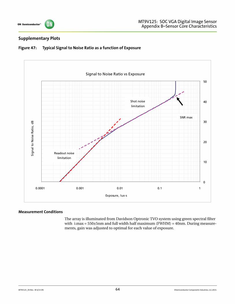
MT9V125: SOC VGA Digital Image SensorAppendix B–Sensor Core Characteristics
Supplementary Plots
Figure 47: Typical Signal to Noise Ratio as a function of Exposure
Measurement Conditions
The array is illuminated from Davidson Optronic TVO system using green spectral filter with max = 550±5nm and full width half maximum (FWHM) = 40nm. During measure-ments, gain was adjusted to optimal for each value of exposure.
Signal to Noise Ratio vs Exposure
0
10
20
30
40
50
0.0001 0.001 0.01 0.1 1
Exposure, lux-s
Sig
nal
to
No
ise
Rati
o,
dB
SNR max
Readout noise
limitation
Shot noise
limitation
MT9V125_DS Rev.. W 6/15 EN 64 ©Semiconductor Components Industries, LLC,2015.
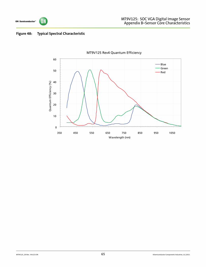
MT9V125: SOC VGA Digital Image SensorAppendix B–Sensor Core Characteristics
Figure 48: Typical Spectral Characteristic
MT9V125 Rev4 Quantum Efficiency
0
10
20
30
40
50
60
350 450 550 650 750 850 950 1050
Wavelength (nm)
Qu
antu
m E
ffic
ien
cy (
%)
BlueGreenRed
MT9V125_DS Rev.. W 6/15 EN 65 ©Semiconductor Components Industries, LLC,2015.
MT9V125: SOC VGA Digital Image SensorRevision History
Revision HistoryRev. W. . . . . . . . . . . . . . . . . . . . . . . . . . . . . . . . . . . . . . . . . . . . . . . . . . . . . . . . . . . . . . . . . . . . . . . . . . . . . . . . . . . . . . . . . . . .6/19/15
• Updated “Ordering Information” on page 2
Rev. V . . . . . . . . . . . . . . . . . . . . . . . . . . . . . . . . . . . . . . . . . . . . . . . . . . . . . . . . . . . . . . . . . . . . . . . . . . . . . . . . . . . . . . . . . . . .4/16/15• Updated “Ordering Information” on page 2
Rev. U . . . . . . . . . . . . . . . . . . . . . . . . . . . . . . . . . . . . . . . . . . . . . . . . . . . . . . . . . . . . . . . . . . . . . . . . . . . . . . . . . . . . . . . . . . . 3/31/15• Converted to ON Semiconductor template.
Rev. T . . . . . . . . . . . . . . . . . . . . . . . . . . . . . . . . . . . . . . . . . . . . . . . . . . . . . . . . . . . . . . . . . . . . . . . . . . . . . . . . . . . . . . . . . . . . . 5/4/11• Updated trademarks• Applied updated template
Rev. S . . . . . . . . . . . . . . . . . . . . . . . . . . . . . . . . . . . . . . . . . . . . . . . . . . . . . . . . . . . . . . . . . . . . . . . . . . . . . . . . . . . . . . . . . . . . . 6/2/10• Updated to non-confidential
Rev. R, Production . . . . . . . . . . . . . . . . . . . . . . . . . . . . . . . . . . . . . . . . . . . . . . . . . . . . . . . . . . . . . . . . . . . . . . . . . . . . . . . . . 5/6/10• Updated to Aptina template• Transfered registers to register reference
Rev. Q, Production . . . . . . . . . . . . . . . . . . . . . . . . . . . . . . . . . . . . . . . . . . . . . . . . . . . . . . . . . . . . . . . . . . . . . . . . . . . . . . . . . 1/3/08• Updated Figure 2: “Typical Usage Configuration with Overlay,” on page 7, moved
labels closed to their respective buses• Added Figure 11 and Figure 12 on page 18 to explain AWB measurement area• Updated description of AWB Window Boundaries in Table 15, “Camera Control
Register—Address Page 2,” on page 63• Updated Figure 29 and Table 13 on page 43• Added Figure 30 and Table 14 on page 44• Updated Figure 3 on page 8• Updated Note 1 in Table 13, “Parallel Input Data Timing Values Using DIN_CLK,” on
page 43
Rev. P, Production . . . . . . . . . . . . . . . . . . . . . . . . . . . . . . . . . . . . . . . . . . . . . . . . . . . . . . . . . . . . . . . . . . . . . . . . . . . . . . . . . . 8/3/07• Added “Appendix B–Sensor Core Characteristics” on page 63.• Added Figure 47: “Typical Signal to Noise Ratio as a function of Exposure,” on page 65.• Added Figure 48: “Typical Spectral Characteristic,” on page 66.• Updated Table 23, “Digital I/O Parameters,” on page 54.• Updated Figure 40 and Figure 41 on page 61.• Updated Figure 45 on page 62.
Rev. N, Production . . . . . . . . . . . . . . . . . . . . . . . . . . . . . . . . . . . . . . . . . . . . . . . . . . . . . . . . . . . . . . . . . . . . . . . . . . . . . . . .4/03/07• Updated Figure 32 on page 49, Figure 33 on page 50, Table 3 on page 9, Table 21 on
page 52 and, Table 22 on page 53.
Rev. M, Production . . . . . . . . . . . . . . . . . . . . . . . . . . . . . . . . . . . . . . . . . . . . . . . . . . . . . . . . . . . . . . . . . . . . . . . . . . . . . . . .3/13/07• Added I/O circuitry diagrams see Figure 32 on page 49 and Figure 33 on page 50.• Re-ordered pads for DIN[7:0] and DOUT[7:0] in Table 3 on page 9.• Updated Figure 34 on page 51.• Fixed typos.• Added DigitalClarity to trademarks on last page.
MT9V125_DS Rev.. W 6/15 EN 67 ©Semiconductor Components Industries, LLC,2015.
MT9V125: SOC VGA Digital Image SensorRevision History
Rev. L, Production. . . . . . . . . . . . . . . . . . . . . . . . . . . . . . . . . . . . . . . . . . . . . . . . . . . . . . . . . . . . . . . . . . . . . . . . . . . . . . . . .1/17/07• Updates to Table 1 on page 1, Table 2 on page 2, and Table 20 on page 51.• Updates to Figure 3 on page 8, Figure 15 on page 25, Figure 19 on page 32.• Updates to Figures 20 through Figure 24 on page 37.• Updates to Figure 34 on page 51.• Added Figure 40 on page 61.• Minor changes for typos throughout document.
Rev. K, Production . . . . . . . . . . . . . . . . . . . . . . . . . . . . . . . . . . . . . . . . . . . . . . . . . . . . . . . . . . . . . . . . . . . . . . . . . . . . . . .11/29/06• Updates to Figure 34 and Table 19 on page 48.• Updates to Table 23 and Table 25 on page 55.
Rev. J, Production . . . . . . . . . . . . . . . . . . . . . . . . . . . . . . . . . . . . . . . . . . . . . . . . . . . . . . . . . . . . . . . . . . . . . . . . . . . . . . . .11/21/06• Updated register/variable information in the following tables: Table 10 on page 30,
Table 11 on page 32, Table 12 on page 34, Table 13 on page 39, Table 14 on page 48, and Table 15 on page 63 for Rev4_3.
• Added ordering information in Table 2 on page 2.
Rev. H, Production . . . . . . . . . . . . . . . . . . . . . . . . . . . . . . . . . . . . . . . . . . . . . . . . . . . . . . . . . . . . . . . . . . . . . . . . . . . . . . . .10/6/06• Changed colors in Figure 1 on page 7, Figure 2 on page 7, Figure 3 on page 8, Figure 5
on page 11, and Figure 6 on page 11.
Rev. G, Production . . . . . . . . . . . . . . . . . . . . . . . . . . . . . . . . . . . . . . . . . . . . . . . . . . . . . . . . . . . . . . . . . . . . . . . . . . . . . . . .8/29/06• Added “Data Sheet Applicable To” on page 1.• Added Table 25, “NTSC Signal Parameters,” on page 55.• Updated See “Sensor Registers—Short Descriptions” on page 30.• Updated register information in Table 13 on page 39, Table 14 on page 48, and
Table 15 on page 63.• Updated package drawing Figure 35: 52-Ball iBGA Package Outline Drawing on
page 56.
Rev. F, Production . . . . . . . . . . . . . . . . . . . . . . . . . . . . . . . . . . . . . . . . . . . . . . . . . . . . . . . . . . . . . . . . . . . . . . . . . . . . . . . . . . 8/1/06• Updated all figures that were not using MarCom standard colors. No technical
content of the figures was changed.• Updated Equation 1 on page 28 through Equation 20 on page 31 using FrameMaker
equation tool.• Many changes were made to make the document more consistent with MarCom stan-
dards.• Latin abbreviations were removed.• NTSC/PAL changed to “NTSC and PAL” or “NTSC or PAL” where appropriate.
Rev. E, Production. . . . . . . . . . . . . . . . . . . . . . . . . . . . . . . . . . . . . . . . . . . . . . . . . . . . . . . . . . . . . . . . . . . . . . . . . . . . . . . . .4/28/06• Updated Table 13 on page 43.• Updated Figure 33 on page 50.• Updated Figure 3 on page 8 and added note about VAA and VAAPIX.• Added note about VAA and VAAPIX to Table 3 on page 9.• Fixed notes in Table 4, Readout Mode Register Settings – Dout Not Qualified and
Table 6, Readout Mode Register Settings – Dout Qualified.• Removed “Preliminary” designation on Figure 20 on page 34, Figure 21 on page 35,
Figure 23 on page 37, and Figure 24 on page 37.• Updated Figure 19 on page 32.
MT9V125_DS Rev.. W 6/15 EN 68 ©Semiconductor Components Industries, LLC,2015.
MT9V125: SOC VGA Digital Image SensorRevision History
Rev. D, Preliminary. . . . . . . . . . . . . . . . . . . . . . . . . . . . . . . . . . . . . . . . . . . . . . . . . . . . . . . . . . . . . . . . . . . . . . . . . . . . . . . .4/06/06• Updated Figure 22 on page 36.
Rev. C, Preliminary . . . . . . . . . . . . . . . . . . . . . . . . . . . . . . . . . . . . . . . . . . . . . . . . . . . . . . . . . . . . . . . . . . . . . . . . . . . . . . .11/3/05• Updated register definitions from Rev1 to Rev2. New register listing formation.• Updated NTSC/PAL termination recommendations with SMTPE Compliant sche-
matics.• Updated "Minimum Horizontal Blanking (in sensor stand-alone mode)" on page 29.• Updated "Maximum Shutter Delay" on page 31.
Rev. B . . . . . . . . . . . . . . . . . . . . . . . . . . . . . . . . . . . . . . . . . . . . . . . . . . . . . . . . . . . . . . . . . . . . . . . . . . . . . . . . . . . . . . . . . . .04/29/05• Updated to Advance• Added Register summaries; updated notation.• Added Register descriptions; updated notation.• Added multiple chapters and art.
Rev A, . . . . . . . . . . . . . . . . . . . . . . . . . . . . . . . . . . . . . . . . . . . . . . . . . . . . . . . . . . . . . . . . . . . . . . . . . . . . . . . . . . . . . . . . . . . . . .02/05• Initial release
ON Semiconductor and the ON logo are registered trademarks of Semiconductor Components Industries, LLC (SCILLC) or its subsidiaries in the United States and/or other countries. SCILLC owns therights to a number of patents, trademarks, copyrights, trade secrets, and other intellectual property. A listing of SCILLC’s product/patent coverage may be accessed at www.onsemi.com/site/pdf/Patent-Marking.pdf. SCILLC reserves the right to make changes without further notice to any products herein. SCILLC makes no warranty, representation or guarantee regarding the suitability of itsproducts for any particular purpose, nor does SCILLC assume any liability arising out of the application or use of any product or circuit, and specifically disclaims any and all liability, includingwithout limitation special, consequential or incidental damages. “Typical” parameters which may be provided in SCILLC data sheets and/or specifications can and do vary in different applicationsand actual performance may vary over time. All operating parameters, including “Typicals” must be validated for each customer application by customer’s technical experts. SCILLC does not conveyany license under its patent rights nor the rights of others. SCILLC products are not designed, intended, or authorized for use as components in systems intended for surgical implant into the body,or other applications intended to support or sustain life, or for any other application in which the failure of the SCILLC product could create a situation where personal injury or death may occur.Should Buyer purchase or use SCILLC products for any such unintended or unauthorized application, Buyer shall indemnify and hold SCILLC and its officers, employees, subsidiaries, affiliates, anddistributors harmless against all claims, costs, damages, and expenses, and reasonable attorney fees arising out of, directly or indirectly, any claim of personal injury or death associated with suchunintended or unauthorized use, even if such claim alleges that SCILLC was negligent regarding the design or manufacture of the part. SCILLC is an Equal Opportunity/Affirmative Action Employer.This literature is subject to all applicable copyright laws and is not for resale in any manner.
MT9V125_DS Rev.. W 6/15 EN 69 ©Semiconductor Components Industries, LLC,2015 .