msp430fg461x, msp430cg461x mixed-signal …€¢ 12-bit analog-to-digital converter ... p3.x/p4.x...
TRANSCRIPT
Product
Folder
Sample &Buy
Technical
Documents
Tools &
Software
Support &Community
ReferenceDesign
MSP430FG4619, MSP430FG4618, MSP430FG4617, MSP430FG4616MSP430CG4619, MSP430CG4618, MSP430CG4617, MSP430CG4616
SLAS508J –APRIL 2006–REVISED JUNE 2015
MSP430FG461x, MSP430CG461x Mixed-Signal Microcontrollers1 Device Overview
1.1 Features1
• Low Supply-Voltage Range: 1.8 V to 3.6 V • Universal Serial Communication Interface• Ultra-Low Power Consumption – Enhanced UART Supports Automatic Baud-
Rate Detection– Active Mode: 400 µA at 1 MHz, 2.2 V– IrDA Encoder and Decoder– Standby Mode: 1.3 µA– Synchronous SPI– Off Mode (RAM Retention): 0.22 µA– I2C• Five Power-Saving Modes
• Serial Onboard Programming, Programmable• Wakeup From Standby Mode in Less Than 6 µsCode Protection by Security Fuse• 16-Bit RISC Architecture, Extended Memory,
• Brownout Detector125‑ns Instruction Cycle Time• Basic Timer With Real-Time Clock (RTC) Feature• Three-Channel Internal DMA• Integrated LCD Driver up to 160 Segments With• 12-Bit Analog-to-Digital Converter (ADC) With
Regulated Charge PumpInternal Reference, Sample-and-Hold andAutoscan Feature • Section 3 Summarizes the Available Family
Members• Three Configurable Operational Amplifiers– MSP430FG4616, MSP430FG4616• Dual 12-Bit Digital-to-Analog Converters (DACs)
92KB+256B of Flash or ROMWith Synchronization4KB of RAM• 16-Bit Timer_A With Three Capture/Compare
– MSP430FG4617, MSP430CG4617Registers92KB+256B of Flash or ROM• 16-Bit Timer_B With Seven Capture/Compare-8KB of RAMWith-Shadow Registers
– MSP430FG4618, MSP430CG4618• On-Chip Comparator116KB+256B of Flash or ROM• Supply Voltage Supervisor and Monitor With 8KB of RAMProgrammable Level Detection
– MSP430FG4619, MSP430CG4619• Serial Communication Interface (USART1), Select 120KB+256B of Flash or ROMAsynchronous UART or Synchronous SPI by 4KB of RAMSoftware• For Complete Module Descriptions, see the
MSP430x4xx Family User’s Guide (SLAU056)
1.2 Applications• Portable Medical Applications • E-Meter Applications
1.3 DescriptionThe TI MSP430™ family of ultra-low-power microcontrollers consists of several devices featuring differentsets of peripherals targeted for various applications. The architecture, combined with five low-powermodes, is optimized to achieve extended battery life in portable measurement applications. The devicefeatures a powerful 16-bit RISC CPU, 16-bit registers, and constant generators that contribute tomaximum code efficiency. The digitally controlled oscillator (DCO) allows the device to wake up from low-power modes to active mode in less than 6 µs.
The MSP430xG461x series are microcontroller configurations with two 16-bit timers, a high-performance12-bit ADC, dual 12-bit DACs, three configurable operational amplifiers, one universal serialcommunication interface (USCI), one universal synchronous/asynchronous communication interface(USART), DMA, 80 I/O pins, and a segment liquid crystal display (LCD) driver with regulated chargepump.
1
An IMPORTANT NOTICE at the end of this data sheet addresses availability, warranty, changes, use in safety-critical applications,intellectual property matters and other important disclaimers. PRODUCTION DATA.

Oscillators
FLL+
RAM
4KB8KB8KB4KB
Brownout
Protection
SVS/SVM
RST/NMI
DVCC 1/2 DVSS1/2
MCLK
Watchdog
WDT+
15/16-Bit
Timer_A3
3 CC
Registers
8MHz
CPUX
incl. 16
Registers
XOUT/
XT2OUT
OA0, OA1,
OA2
3 Op Amps
Basic Timerand
Real-TimeClock
JTAG
Interface
LCD_A
160
Segments
1,2,3,4 Mux
PortsP1/P2
2x8 I/O
Interruptcapability
USCI_A0:
UART,IrDA, SPI
USCI_B0:SPI, I2C
Comparator
_A
Flash (FG)ROM (CG)
120KB116KB92KB92KB
Hardware
Multiplier
MPY,
MPYS,
MAC,
MACS
Timer_B7
7 CC
Registers,
Shadow
Reg
ADC12
12-Bit
12
Channels
DAC12
12-Bit
2 Channels
Voltage out
USART 1
UART , SPI
DMA
Controller
3 Channels
PortsP3/P4P5/P6
4x8 I/O
PortsP7/P8
P9/P10
4x8, 2x16 I/O
AVCC AVSS P1.x/P2.x
2x8
P3.x/P4.x
P5.x/P6.x
4x8
P7.x/P8.x
P9.x/P10.x
4x8/2x16
XIN /
XT2IN
22
SMCLK
ACLK
MDB
MAB
Enhanced
Emulation
(FG only )
MSP430FG4619, MSP430FG4618, MSP430FG4617, MSP430FG4616MSP430CG4619, MSP430CG4618, MSP430CG4617, MSP430CG4616SLAS508J –APRIL 2006–REVISED JUNE 2015 www.ti.com
Device Information (1)
PART NUMBER PACKAGE BODY SIZE (2)
MSP430FG4619IPZ LQFP (100) 14 mm × 14 mmMSP430FG4619IZQW MicroStar Junior™ BGA (113) 7 mm × 7 mm
(1) For the most current part, package, and ordering information for all available devices, see the PackageOption Addendum in Section 8, or see the TI website at www.ti.com.
(2) The sizes shown here are approximations. For the package dimensions with tolerances, see theMechanical Data in Section 8.
1.4 Functional Block DiagramFigure 1-1 shows the functional block diagram.
Figure 1-1. Functional Block Diagram
2 Device Overview Copyright © 2006–2015, Texas Instruments IncorporatedSubmit Documentation Feedback
Product Folder Links: MSP430FG4619 MSP430FG4618 MSP430FG4617 MSP430FG4616 MSP430CG4619MSP430CG4618 MSP430CG4617 MSP430CG4616
MSP430FG4619, MSP430FG4618, MSP430FG4617, MSP430FG4616MSP430CG4619, MSP430CG4618, MSP430CG4617, MSP430CG4616
www.ti.com SLAS508J –APRIL 2006–REVISED JUNE 2015
Table of Contents1 Device Overview ......................................... 1 5.30 12-Bit ADC, Timing Parameters .................... 37
1.1 Features .............................................. 1 5.31 12-Bit ADC, Linearity Parameters................... 375.32 12-Bit ADC, Temperature Sensor and Built-In VMID1.2 Applications........................................... 1
...................................................... 381.3 Description............................................ 15.33 12-Bit DAC, Supply Specifications .................. 381.4 Functional Block Diagram ............................ 25.34 12-Bit DAC, Linearity Specifications ................ 392 Revision History ......................................... 45.35 12-Bit DAC, Output Specifications .................. 413 Device Comparison ..................................... 55.36 12-Bit DAC, Reference Input Specifications ........ 414 Terminal Configuration and Functions.............. 65.37 12-Bit DAC, Dynamic Specifications ................ 424.1 Pin Diagrams ......................................... 65.38 12-Bit DAC, Dynamic Specifications Continued .... 434.2 Signal Descriptions ................................... 85.39 Operational Amplifier OA, Supply Specifications ... 445 Specifications ........................................... 145.40 Operational Amplifier OA, Input/Output5.1 Absolute Maximum Ratings ........................ 14
Specifications........................................ 445.2 ESD Ratings ........................................ 14
5.41 Operational Amplifier OA, Dynamic Specifications . 455.3 Recommended Operating Conditions............... 14
5.42 Operational Amplifier OA, Typical Characteristics .. 455.4 Supply Current Into AVCC + DVCC Excluding
5.43 Operational Amplifier OA Feedback Network,External Current .................................... 16Noninverting Amplifier Mode (OAFCx = 4).......... 46
5.5 Thermal Characteristics ............................. 17 5.44 Operational Amplifier OA Feedback Network,5.6 Schmitt-Trigger Inputs – Ports P1 to P10, RST/NMI, Inverting Amplifier Mode (OAFCx = 6) .............. 46
JTAG (TCK, TMS, TDI/TCLK,TDO/TDI) ............ 185.45 Flash Memory (FG461x Devices Only) ............. 47
5.7 Inputs Px.x, TAx, TBX............................... 185.46 JTAG Interface ...................................... 47
5.8 Leakage Current – Ports P1 to P10 ................ 185.47 JTAG Fuse ......................................... 47
5.9 Outputs – Ports P1 to P10 .......................... 18 6 Detailed Description ................................... 485.10 Output Frequency ................................... 19
6.1 CPU ................................................. 485.11 Typical Characteristics – Outputs ................... 20
6.2 Instruction Set....................................... 495.12 Wake-up Timing From LPM3 ....................... 21
6.3 Operating Modes.................................... 505.13 RAM ................................................. 21
6.4 Interrupt Vector Addresses.......................... 515.14 LCD_A............................................... 21
6.5 Special Function Registers (SFRs) ................. 525.15 Comparator_A ...................................... 22
6.6 Memory Organization ............................... 545.16 Typical Characteristics – Comparator_A............ 23
6.7 Bootstrap Loader (BSL) ............................. 555.17 POR, BOR .......................................... 24
6.8 Flash Memory ....................................... 555.18 SVS (Supply Voltage Supervisor and Monitor) ..... 25
6.9 Peripherals .......................................... 555.19 DCO ................................................. 27
6.10 Input/Output Schematics ............................ 655.20 Crystal Oscillator, LFXT1 Oscillator ................ 29 7 Device and Documentation Support .............. 1005.21 Crystal Oscillator, XT2 Oscillator ................... 29
7.1 Device Support..................................... 1005.22 USCI (UART Mode) ................................. 29
7.2 Documentation Support............................ 1035.23 USCI (SPI Master Mode)............................ 30
7.3 Related Links ...................................... 1035.24 USCI (SPI Slave Mode) ............................. 30
7.4 Community Resources............................. 1045.25 USCI (I2C Mode) .................................... 33
7.5 Trademarks ........................................ 1045.26 USART1 ............................................. 33
7.6 Electrostatic Discharge Caution ................... 1045.27 12-Bit ADC, Power Supply and Input Range
7.7 Export Control Notice .............................. 104Conditions .......................................... 347.8 Glossary............................................ 1045.28 12-Bit ADC, External Reference ................... 34
8 Mechanical, Packaging, and Orderable5.29 12-Bit ADC, Built-In Reference...................... 35Information ............................................. 105
Copyright © 2006–2015, Texas Instruments Incorporated Table of Contents 3Submit Documentation Feedback
Product Folder Links: MSP430FG4619 MSP430FG4618 MSP430FG4617 MSP430FG4616 MSP430CG4619MSP430CG4618 MSP430CG4617 MSP430CG4616

MSP430FG4619, MSP430FG4618, MSP430FG4617, MSP430FG4616MSP430CG4619, MSP430CG4618, MSP430CG4617, MSP430CG4616SLAS508J –APRIL 2006–REVISED JUNE 2015 www.ti.com
2 Revision HistoryNOTE: Page numbers for previous revisions may differ from page numbers in the current version.
Changes from March 2, 2011 to June 19, 2015 Page
• Document format and organization changes throughout, including the addition of section numbering ................... 1• Added Device Information table .................................................................................................... 2• Moved functional block diagram to Section 1.4................................................................................... 2• Added Section 3, Device Comparison ............................................................................................. 5• Added signal names to ZQW pinout figure ........................................................................................ 7• Changed table note that starts "Segments S0 through S3 are disabled when..."............................................ 8• Added row for unassigned ball locations on ZQW package ................................................................... 13• Added Section 5 and moved all electrical specifications to it ................................................................. 14• Added Section 5.2, ESD Ratings.................................................................................................. 14• In Recommended Operating Conditions, added test conditions for TYP values ........................................... 14• Added Section 5.5, Thermal Characteristics .................................................................................... 17• Changed table note that starts "Segments S0 through S3 are disabled when..." .......................................... 21• Changed the value of DAC12_xDAT from 7F7h to F7Fh in Figure 5-33 .................................................... 43• Added Table 6-19 and moved P4.6 and P4.7 from Table 6-18 to insert correct LCDS32 control bit name ............ 75• Added Table 6-29 and moved P7.2 and P7.3 from Table 6-28 to insert correct LCDS28 control bit name ............ 88• Added Table 6-31 and moved P7.6 and P7.7 from Table 6-30 to insert correct LCDS24 control bit name ............ 89• Added Table 6-33 and moved P8.2 to P8.5 from Table 6-32 to insert correct LCDS20 control bit name............... 90• Added Table 6-36 and moved P9.2 to P9.5 from Table 6-35 to insert correct LCDS12 control bit name............... 92• Corrected LCD segment numbers in PIN NAME column of Table 6-36 ..................................................... 92• Added Table 6-37 and moved P9.6 and P9.7 from Table 6-35 to insert correct LCDS8 control bit name .............. 93• Corrected LCD segment numbers in PIN NAME column of Table 6-37 ..................................................... 93• Corrected LCD segment numbers in PIN NAME and FUNCTION columns of Table 6-38................................ 94• Added Table 6-39 and moved P10.2 to P10.5 from Table 6-38 to insert correct LCDS4 control bit name ............. 94• Added Section 7 and moved Trademarks and ESD Caution sections to it ................................................ 100• Added Section 8 ................................................................................................................... 105
4 Revision History Copyright © 2006–2015, Texas Instruments IncorporatedSubmit Documentation Feedback
Product Folder Links: MSP430FG4619 MSP430FG4618 MSP430FG4617 MSP430FG4616 MSP430CG4619MSP430CG4618 MSP430CG4617 MSP430CG4616

MSP430FG4619, MSP430FG4618, MSP430FG4617, MSP430FG4616MSP430CG4619, MSP430CG4618, MSP430CG4617, MSP430CG4616
www.ti.com SLAS508J –APRIL 2006–REVISED JUNE 2015
3 Device Comparison
Table 3-1 summarizes the available family members.
Table 3-1. Device Comparison (1) (2)
FLASH ROM RAM ADC12 DAC12 COMP_ADEVICE EEM Timer_A Timer_B OP AMP USART USCI I/O PACKAGE(KB) (KB) (KB) (Channels) (Channels) (Channels)PZ 100MSP430FG4619 120 – 4 1 TA3 TB7 12 3 2 2 1 A0, B0 80 ZQW 113PZ 100MSP430FG4618 116 – 8 1 TA3 TB7 12 3 2 2 1 A0, B0 80 ZQW 113PZ 100MSP430FG4617 92 – 8 1 TA3 TB7 12 3 2 2 1 A0, B0 80 ZQW 113PZ 100MSP430FG4616 92 – 4 1 TA3 TB7 12 3 2 2 1 A0, B0 80 ZQW 113PZ 100MSP430CG4619 – 120 4 – TA3 TB7 12 3 2 2 1 A0, B0 80 ZQW 113PZ 100MSP430CG4618 – 116 8 – TA3 TB7 12 3 2 2 1 A0, B0 80 ZQW 113PZ 100MSP430CG4617 – 92 8 – TA3 TB7 12 3 2 2 1 A0, B0 80 ZQW 113PZ 100MSP430CG4616 – 92 4 – TA3 TB7 12 3 2 2 1 A0, B0 80 ZQW 113
(1) For the most current device, package, and ordering information for all available devices, see the Package Option Addendum in Section 8, or see the TI website at www.ti.com.(2) Package drawings, thermal data, and symbolization are available at www.ti.com/packaging.
Copyright © 2006–2015, Texas Instruments Incorporated Device Comparison 5Submit Documentation Feedback
Product Folder Links: MSP430FG4619 MSP430FG4618 MSP430FG4617 MSP430FG4616 MSP430CG4619MSP430CG4618 MSP430CG4617 MSP430CG4616

1
2
3
4
5
6
7
8
9
10
11
12
13
14
15
16
17
18
19
20
21
22
23
24
25
76
77
78
79
80
81
82
83
84
85
86
87
88
89
90
91
92
93
94
95
96
97
98
99
10
0
75
74
73
72
71
70
69
68
67
66
65
64
63
62
61
60
59
58
57
56
55
54
53
52
51
50
49
48
47
46
45
44
43
42
41
40
39
38
37
36
35
34
33
32
31
30
29
28
27
26
P1
.7/C
A1
P6
.1/A
1/O
A0
O
P6
.0/A
0/O
A0
I0
RS
T/N
MI
XT
2IN
XT
2O
UT
P1
.3/T
BO
UT
H/S
VS
OU
T
P1
.4/T
BC
LK
/SM
CL
K
P1
.5/T
AC
LK
/AC
LK
P1
.6/C
A0
P2
.3/T
B2
P9
,2/S
15
P9
.1/S
16
P9
.0/S
17
P8
.5/S
20
P8
.0/S
25
P7
.7/S
26
P7
.6/S
27
P7
.5/S
28
P7
.4/S
29
P7
.2/U
CA
0S
OM
I/S
31
P4
.7/U
CA
0R
XD
/S3
4
P7
.3/U
CA
0C
LK
/S3
0
P1
.0/T
A0
TD
I/T
CL
K
TD
O/T
DI
P8
.4/S
21
SS
1D
V
P6
.2/A
2/O
A0
I1
P1
.2/T
A1
P8
.1/S
24
P4
.6/U
CA
0T
XD
/S3
5
DVCC1
P6.3/A3/OA1O
P6.4/A4/OA1I0
P6.5/A5/OA2O
P6.6/A6/DAC0/OA2I0
P6.7/A7/DAC1/SVSIN
VREF+
XIN
XOUT
VeREF+/DAC0
VREF-/VeREF-
P5.1/S0/A12/DAC1
P5.0/S1/A13/OA1I1
P10.7/S2/A14/OA2I1
P10.6/S3/A15
P10.5/S4
P10.4/S5
P10.3/S6
P10.2/S7
P10.1/S8
P10.0/S9
P9.7/S10
P9.6/S11
P9.5/S12
P9.4/S13
P2.4/UCA0TXD
P2.5/UCA0RXD
P2.6/CAOUT
P2.7/ADC12CLK/DMAE0
P3.0/UCB0STE
P3.1/UCB0SIMO/UCB0SDA
P3.2/UCB0SOMI/UCB0SCL
P3.3/UCB0CLK
P3.4/TB3
P3.5/TB4
P3.6/TB5
P3.7/TB6
P4.0/UTXD1
P4.1/URXD1
DVSS2
DVCC2
LCDCAP/R33
P5.7/R23
P5.6/LCDREF/R13
P5.5/R03
P5.4/COM3
P5.3/COM2
P5.2/COM1
COM0
P4.2/STE1/S39
P8
.6/S
19
P8
.3/S
22
P8
.2/S
23
P7
.0/U
CA
0S
TE
/S3
3
P7
.1/U
CA
0S
IMO
/S3
2
P4
.5/U
CL
K1
/S3
6
P4
.4/S
OM
I1/S
37
P4
.3/S
IMO
1/S
38
CC
AV
SS
AV
TC
K
TM
S
P1
.1/T
A0
/MC
LK
P2
.0/T
A2
P2
.1/T
B0
P2
.2/T
B1
P9.3
/S14
P8.7
/S18
MSP430FG4619, MSP430FG4618, MSP430FG4617, MSP430FG4616MSP430CG4619, MSP430CG4618, MSP430CG4617, MSP430CG4616SLAS508J –APRIL 2006–REVISED JUNE 2015 www.ti.com
4 Terminal Configuration and Functions
4.1 Pin DiagramsFigure 4-1 shows the pinout for the 100-pin PZ package.
Figure 4-1. 100-Pin PZ Package (Top View)
6 Terminal Configuration and Functions Copyright © 2006–2015, Texas Instruments IncorporatedSubmit Documentation Feedback
Product Folder Links: MSP430FG4619 MSP430FG4618 MSP430FG4617 MSP430FG4616 MSP430CG4619MSP430CG4618 MSP430CG4617 MSP430CG4616

A
B
C
D
E
F
G
H
J
K
L
M
1 2 3 4 5 6 7 8 9 10 11 12
DVCC1
P6.3
P6.6
XIN
XOUT
P5.1
P10.6
P10.3
P10.0
P9.5
P9.4
N/A
AVCC
P6.4
P6.5
VREF+
VeREF+
P5.0
P10.5
P10.2
P9.7
P9.2
N/A
P9.3
AVSS
DVSS1
P6.7
P9.1
P9.0
P6.0
P6.2
N/A
VREF–
P10.4
P9.6
P8.7
N/A
P8.6
P8.5
TCK
RST
P6.1
P10.7
P10.1
P8.4
P8.1
P8.0
P8.3
P8.2
TDO
XT2IN
TDI
TMS
P7.3
P7.5
P7.6
P7.7
P1.0
XT2OUT
P1.2
P1.1
P4.4
P4.7
P7.2
P7.4
P1.3
P1.4
P2.1
P2.2
N/A
N/A
N/A
P5.3
P7.0
P7.1
P1.6
P1.5
N/A
P2.7
P3.2
P3.5
P4.0
N/A
P4.5
P4.6
P2.0
P1.7
COM0
P4.3
P2.3
N/A
P2.5
P3.0
P3.3
P3.6
P4.1
LCDCAP
P5.7
P5.5
N/A
P4.2
N/A
P2.4
P2.6
P3.1
P3.4
P3.7
DVSS2
DVCC2
P5.6
P5.4
P5.2
N/A
MSP430FG4619, MSP430FG4618, MSP430FG4617, MSP430FG4616MSP430CG4619, MSP430CG4618, MSP430CG4617, MSP430CG4616
www.ti.com SLAS508J –APRIL 2006–REVISED JUNE 2015
Figure 4-2 shows the pinout for the 113-pin ZQW package. This figure shows only the default pinassignments; for all pin assignments, see Table 4-1.
N/A = Not Assigned. All unassigned ball locations on the ZQW package should be electrically tied to the groundsupply. The shortest ground return path to the device should be established to ball location B3, DVSS1.
Figure 4-2. 113-Pin ZQW Package (Top View)
Copyright © 2006–2015, Texas Instruments Incorporated Terminal Configuration and Functions 7Submit Documentation Feedback
Product Folder Links: MSP430FG4619 MSP430FG4618 MSP430FG4617 MSP430FG4616 MSP430CG4619MSP430CG4618 MSP430CG4617 MSP430CG4616

MSP430FG4619, MSP430FG4618, MSP430FG4617, MSP430FG4616MSP430CG4619, MSP430CG4618, MSP430CG4617, MSP430CG4616SLAS508J –APRIL 2006–REVISED JUNE 2015 www.ti.com
4.2 Signal DescriptionsTable 4-1 describes the signals for all device variants and package options.
Table 4-1. Signal DescriptionsPIN NO.
SIGNAL NAME I/O DESCRIPTIONPZ ZQW
DVCC1 1 A1 Digital supply voltage, positive terminalP6.3 General-purpose digital I/OA3 2 B1 I/O Analog input A3 for 12-bit ADCOA1O OA1 outputP6.4 General-purpose digital I/OA4 3 B2 I/O Analog input A4 for 12-bit ADCOA1I0 OA1 input multiplexer on + terminal and – terminalP6.5 General-purpose digital I/OA5 4 C2 I/O Analog input A5 for 12-bit ADCOA2O OA2 outputP6.6 General-purpose digital I/OA6 Analog input A6 for 12-bit ADC
5 C1 I/ODAC0 DAC12.0 outputOA2I0 OA2 input multiplexer on + terminal and – terminalP6.7 General-purpose digital I/OA7 Analog input A7 for 12-bit ADC
6 C3 I/ODAC1 DAC12.1 outputSVSIN Analog input to brownout, supply voltage supervisorVREF+ 7 D2 O Output of positive terminal of the reference voltage in the ADCXIN 8 D1 I Input port for crystal oscillator XT1. Standard or watch crystals can be connected.XOUT 9 E1 O Output terminal of crystal oscillator XT1VeREF+ Input for an external reference voltage to the ADC
10 E2 I/ODAC0 DAC12.0 outputVREF Internal reference voltage, negative terminal for the ADC reference voltage
11 E4 IVeREF– External applied reference voltage, negative terminal for the ADC reference voltageP5.1 General-purpose digital I/OS0 (1) LCD segment output 0
12 F1 I/OA12 Analog input A12 for 12-bit ADCDAC1 DAC12.1 outputP5.0 General-purpose digital I/OS1 (1) LCD segment output 1
13 F2 I/OA13 Analog input A13 for 12-bit ADCOA1I1 OA1 input multiplexer on + terminal and – terminalP10.7 General-purpose digital I/OS2 (1) LCD segment output 2
14 E5 I/OA14 Analog input A14 for 12-bit ADCOA2I1 OA2 input multiplexer on + terminal and – terminalP10.6 General-purpose digital I/OS3 (1) 15 G1 I/O LCD segment output 3A15 Analog input A15 to 12-bit ADC
(1) Segments S0 through S3 are disabled when the LCD charge pump feature is enabled (LCDCPEN = 1) and, therefore, cannot be usedtogether with the LCD charge pump. On the MSP430xG461x devices only, S0 through S3 are also disabled if VLCDEXT = 1. Thissetting is typically used to apply an external LCD voltage supply to the LCDCAP terminal. For these devices, set LCDCPEN = 0,VLCDEXT = 0, and VLCDx > 0 to enable an external LCD voltage supply to be applied to the LCDCAP terminal.
8 Terminal Configuration and Functions Copyright © 2006–2015, Texas Instruments IncorporatedSubmit Documentation Feedback
Product Folder Links: MSP430FG4619 MSP430FG4618 MSP430FG4617 MSP430FG4616 MSP430CG4619MSP430CG4618 MSP430CG4617 MSP430CG4616

MSP430FG4619, MSP430FG4618, MSP430FG4617, MSP430FG4616MSP430CG4619, MSP430CG4618, MSP430CG4617, MSP430CG4616
www.ti.com SLAS508J –APRIL 2006–REVISED JUNE 2015
Table 4-1. Signal Descriptions (continued)PIN NO.
SIGNAL NAME I/O DESCRIPTIONPZ ZQW
P10.5 General-purpose digital I/O16 G2 I/O
S4 LCD segment output 4P10.4 General-purpose digital I/O
17 F4 I/OS5 LCD segment output 5P10.3 General-purpose digital I/O
18 H1 I/OS6 LCD segment output 6P10.2 General-purpose digital I/O
19 H2 I/OS7 LCD segment output 7P10.1 General-purpose digital I/O
20 F5 I/OS8 LCD segment output 8P10.0 General-purpose digital I/O
21 J1 I/OS9 LCD segment output 9P9.7 General-purpose digital I/O
22 J2 I/OS10 LCD segment output 10P9.6 General-purpose digital I/O
23 G4 I/OS11 LCD segment output 11P9.5 General-purpose digital I/O
24 K1 I/OS12 LCD segment output 12P9.4 General-purpose digital I/O
25 L1 I/OS13 LCD segment output 13P9.3 General-purpose digital I/O
26 M2 I/OS14 LCD segment output 14P9.2 General-purpose digital I/O
27 K2 I/OS15 LCD segment output 15P9.1 General-purpose digital I/O
28 L3 I/OS16 LCD segment output 16P9.0 General-purpose digital I/O
29 M3 I/OS17 LCD segment output 17P8.7 General-purpose digital I/O
30 H4 I/OS18 LCD segment output 18P8.6 General-purpose digital I/O
31 L4 I/OS19 LCD segment output 19P8.5 General-purpose digital I/O
32 M4 I/OS20 LCD segment output 20P8.4 General-purpose digital I/O
33 G5 I/OS21 LCD segment output 21P8.3 General-purpose digital I/O
34 L5 I/OS22 LCD segment output 22P8.2 General-purpose digital I/O
35 M5 I/OS23 LCD segment output 23P8.1 General-purpose digital I/O
36 H5 I/OS24 LCD segment output 24P8.0 General-purpose digital I/O
37 J5 I/OS25 LCD segment output 25P7.7 General-purpose digital I/O
38 M6 I/OS26 LCD segment output 26
Copyright © 2006–2015, Texas Instruments Incorporated Terminal Configuration and Functions 9Submit Documentation Feedback
Product Folder Links: MSP430FG4619 MSP430FG4618 MSP430FG4617 MSP430FG4616 MSP430CG4619MSP430CG4618 MSP430CG4617 MSP430CG4616

MSP430FG4619, MSP430FG4618, MSP430FG4617, MSP430FG4616MSP430CG4619, MSP430CG4618, MSP430CG4617, MSP430CG4616SLAS508J –APRIL 2006–REVISED JUNE 2015 www.ti.com
Table 4-1. Signal Descriptions (continued)PIN NO.
SIGNAL NAME I/O DESCRIPTIONPZ ZQW
P7.6 General-purpose digital I/O39 L6 I/O
S27 LCD segment output 27P7.5 General-purpose digital I/O
40 J6 I/OS28 LCD segment output 28P7.4 General-purpose digital I/O
41 M7 I/OS29 LCD segment output 29P7.3 General-purpose digital I/OUCA0CLK External clock input – USCI_A0 in UART or SPI mode,42 H6 I/O Clock output – USCI_A0 in SPI modeS30 LCD segment 30P7.2 General-purpose digital I/OUCA0SOMI 43 L7 I/O Slave out/master in of USCI_A0 in SPI modeS31 LCD segment output 31P7.1 General-purpose digital I/OUCA0SIMO 44 M8 I/O Slave in/master out of USCI_A0 in SPI modeS32 LCD segment output 32P7.0 General-purpose digital I/OUCA0STE 45 L8 I/O Slave transmit enable – USCI_A0 in SPI modeS33 LCD segment output 33P4.7 General-purpose digital I/OUCA0RXD 46 J7 I/O Receive data in – USCI_A0 in UART or IrDA modeS34 LCD segment output 34P4.6 General-purpose digital I/OUCA0TXD 47 M9 I/O Transmit data out – USCI_A0 in UART or IrDA modeS35 LCD segment output 35P4.5 General-purpose digital I/OUCLK1 External clock input – USART1 in UART or SPI mode,48 L9 I/O Clock output – USART1 in SPI MODES36 LCD segment output 36P4.4 General-purpose digital I/OSOMI1 49 H7 I/O Slave out/master in of USART1 in SPI modeS37 LCD segment output 37P4.3 General-purpose digital I/OSIMO1 50 M10 I/O Slave in/master out of USART1 in SPI modeS38 LCD segment output 38P4.2 General-purpose digital I/OSTE1 51 M11 I/O Slave transmit enable – USART1 in SPI modeS39 LCD segment output 39COM0 52 L10 O Common output, COM0 for LCD backplanesP5.2 General-purpose digital I/O
53 L12 I/OCOM1 Common output, COM1 for LCD backplanesP5.3 General-purpose digital I/O
54 J8 I/OCOM2 Common output, COM2 for LCD backplanesP5.4 General-purpose digital I/O
55 K12 I/OCOM3 Common output, COM3 for LCD backplanesP5.5 General-purpose digital I/O
56 K11 I/OR03 Input port of lowest analog LCD level (V5)
10 Terminal Configuration and Functions Copyright © 2006–2015, Texas Instruments IncorporatedSubmit Documentation Feedback
Product Folder Links: MSP430FG4619 MSP430FG4618 MSP430FG4617 MSP430FG4616 MSP430CG4619MSP430CG4618 MSP430CG4617 MSP430CG4616

MSP430FG4619, MSP430FG4618, MSP430FG4617, MSP430FG4616MSP430CG4619, MSP430CG4618, MSP430CG4617, MSP430CG4616
www.ti.com SLAS508J –APRIL 2006–REVISED JUNE 2015
Table 4-1. Signal Descriptions (continued)PIN NO.
SIGNAL NAME I/O DESCRIPTIONPZ ZQW
P5.6 General-purpose digital I/OLCDREF 57 J12 I/O External reference voltage input for regulated LCD voltageR13 Input port of third most positive analog LCD level (V4 or V3)P5.7 General-purpose digital I/O
58 J11 I/OR23 Input port of second most positive analog LCD level (V2)LCDCAP LCD capacitor connection
59 H11 IR33 Input/output port of most positive analog LCD level (V1)DVCC2 60 H12 Digital supply voltage, positive terminalDVSS2 61 G12 Digital supply voltage, negative terminalP4.1 General-purpose digital I/O
62 G11 I/OURXD1 Receive data in – USART1 in UART modeP4.0 General-purpose digital I/O
63 H9 I/OUTXD1 Transmit data out – USART1 in UART modeP3.7 General-purpose digital I/O
64 F12 I/OTB6 Timer_B7 CCR6. Capture: CCI6A/CCI6B input, compare: Out6 outputP3.6 General-purpose digital I/O
65 F11 I/OTB5 Timer_B7 CCR5. Capture: CCI5A/CCI5B input, compare: Out5 outputP3.5 General-purpose digital I/O
66 G9 I/OTB4 Timer_B7 CCR4. Capture: CCI4A/CCI4B input, compare: Out4 outputP3.4 General-purpose digital I/O
67 E12 I/OTB3 Timer_B7 CCR3. Capture: CCI3A/CCI3B input, compare: Out3 outputP3.3 General-purpose digital I/O
68 E11 I/OUCB0CLK External clock input – USCI_B0 in UART or SPI mode,Clock output – USCI_B0 in SPI mode
P3.2 General-purpose digital I/OUCB0SOMI 69 F9 I/O Slave out/master in of USCI_B0 in SPI modeUCB0SCL I2C clock – USCI_B0 in I2C modeP3.1 General-purpose digital I/OUCB0SIMO 70 D12 I/O Slave in/master out of USCI_B0 in SPI modeUCB0SDA I2C data – USCI_B0 in I2C modeP3.0 General-purpose digital I/O
71 D11 I/OUCB0STE Slave transmit enable – USCI_B0 in SPI modeP2.7 General-purpose digital I/OADC12CLK 72 E9 I/O Conversion clock for 12-bit ADCDMAE0 DMA channel 0 external triggerP2.6 General-purpose digital I/O
73 C12 I/OCAOUT Comparator_A outputP2.5 General-purpose digital I/O
74 C11 I/OUCA0RXD Receive data in – USCI_A0 in UART or IrDA modeP2.4 General-purpose digital I/O
75 B12 I/OUCA0TXD Transmit data out – USCI_A0 in UART or IrDA modeP2.3 General-purpose digital I/O
76 A11 I/OTB2 Timer_B7 CCR2. Capture: CCI2A/CCI2B input, compare: Out2 outputP2.2 General-purpose digital I/O
77 E8 I/OTB1 Timer_B7 CCR1. Capture: CCI1A/CCI1B input, compare: Out1 outputP2.1 General-purpose digital I/O
78 D8 I/OTB0 Timer_B7 CCR0. Capture: CCI0A/CCI0B input, compare: Out0 output
Copyright © 2006–2015, Texas Instruments Incorporated Terminal Configuration and Functions 11Submit Documentation Feedback
Product Folder Links: MSP430FG4619 MSP430FG4618 MSP430FG4617 MSP430FG4616 MSP430CG4619MSP430CG4618 MSP430CG4617 MSP430CG4616

MSP430FG4619, MSP430FG4618, MSP430FG4617, MSP430FG4616MSP430CG4619, MSP430CG4618, MSP430CG4617, MSP430CG4616SLAS508J –APRIL 2006–REVISED JUNE 2015 www.ti.com
Table 4-1. Signal Descriptions (continued)PIN NO.
SIGNAL NAME I/O DESCRIPTIONPZ ZQW
P2.0 General-purpose digital I/O79 A10 I/O
TA2 Timer_A Capture: CCI2A input, compare: Out2 outputP1.7 General-purpose digital I/O
80 B10 I/OCA1 Comparator_A inputP1.6 General-purpose digital I/O
81 A9 I/OCA0 Comparator_A inputP1.5 General-purpose digital I/OTACLK 82 B9 I/O Timer_A, clock signal TACLK inputACLK ACLK output (divided by 1, 2, 4, or 8)P1.4 General-purpose digital I/OTBCLK 83 B8 I/O Input clock TBCLK – Timer_B7SMCLK Submain system clock SMCLK outputP1.3 General-purpose digital I/OTBOUTH 84 A8 I/O Switch all PWM digital output ports to high impedance – Timer_B7 TB0 to TB6SVSOUT SVS: output of SVS comparatorP1.2 General-purpose digital I/O
85 D7 I/OTA1 Timer_A, Capture: CCI1A input, compare: Out1 outputP1.1 General-purpose digital I/OTA0 86 E7 I/O Timer_A. Capture: CCI0B input. Note: TA0 is only an input on this pin. BSL receive.MCLK MCLK outputP1.0 General-purpose digital I/O
87 A7 I/OTA0 Timer_A. Capture: CCI0A input, compare: Out0 output. BSL transmit.XT2OUT 88 B7 O Output terminal of crystal oscillator XT2XT2IN 89 B6 I Input port for crystal oscillator XT2. Only standard crystals can be connected.TDO Test data output port. TDO/TDI data output.
90 A6 I/OTDI Programming data input terminalTDI Test data input
91 D6 ITCLK Test clock input. The device protection fuse is connected to TDI/TCLK.TMS 92 E6 I Test mode select. TMS is used as an input port for device programming and test.TCK 93 A5 I Test clock. TCK is the clock input port for device programming and test.RST Reset input
94 B5 INMI Nonmaskable interrupt input portP6.0 General-purpose digital I/OA0 95 A4 I/O Analog input A0 for 12-bit ADCOA0I0 OA0 input multiplexer on + terminal and – terminalP6.1 General-purpose digital I/OA1 96 D5 I/O Analog input A1 for 12-bit ADCOA0O OA0 outputP6.2 General-purpose digital I/OA2 97 B4 I/O Analog input A2 for 12-bit ADCOA0I1 OA0 input multiplexer on + terminal and – terminal
Analog supply voltage, negative terminal. Supplies SVS, brownout, oscillator,AVSS 98 A3 Comparator_A, port 1DVSS1 99 B3 Digital supply voltage, negative terminal
Analog supply voltage, positive terminal. Supplies SVS, brownout, oscillator,AVCC 100 A2 Comparator_A, port 1. Do not power up before powering DVCC1 and DVCC2.
12 Terminal Configuration and Functions Copyright © 2006–2015, Texas Instruments IncorporatedSubmit Documentation Feedback
Product Folder Links: MSP430FG4619 MSP430FG4618 MSP430FG4617 MSP430FG4616 MSP430CG4619MSP430CG4618 MSP430CG4617 MSP430CG4616
MSP430FG4619, MSP430FG4618, MSP430FG4617, MSP430FG4616MSP430CG4619, MSP430CG4618, MSP430CG4617, MSP430CG4616
www.ti.com SLAS508J –APRIL 2006–REVISED JUNE 2015
Table 4-1. Signal Descriptions (continued)PIN NO.
SIGNAL NAME I/O DESCRIPTIONPZ ZQW
A12,B11, D4,D9, F8, All unassigned ball locations on the ZQW package should be electrically tied to the ground
Not Assigned – G8, H8, – supply. The shortest ground return path to the device should be established to ball locationJ4, J9, B3, DVSS1.
L2, L11,M1, M12
Copyright © 2006–2015, Texas Instruments Incorporated Terminal Configuration and Functions 13Submit Documentation Feedback
Product Folder Links: MSP430FG4619 MSP430FG4618 MSP430FG4617 MSP430FG4616 MSP430CG4619MSP430CG4618 MSP430CG4617 MSP430CG4616
MSP430FG4619, MSP430FG4618, MSP430FG4617, MSP430FG4616MSP430CG4619, MSP430CG4618, MSP430CG4617, MSP430CG4616SLAS508J –APRIL 2006–REVISED JUNE 2015 www.ti.com
5 Specifications
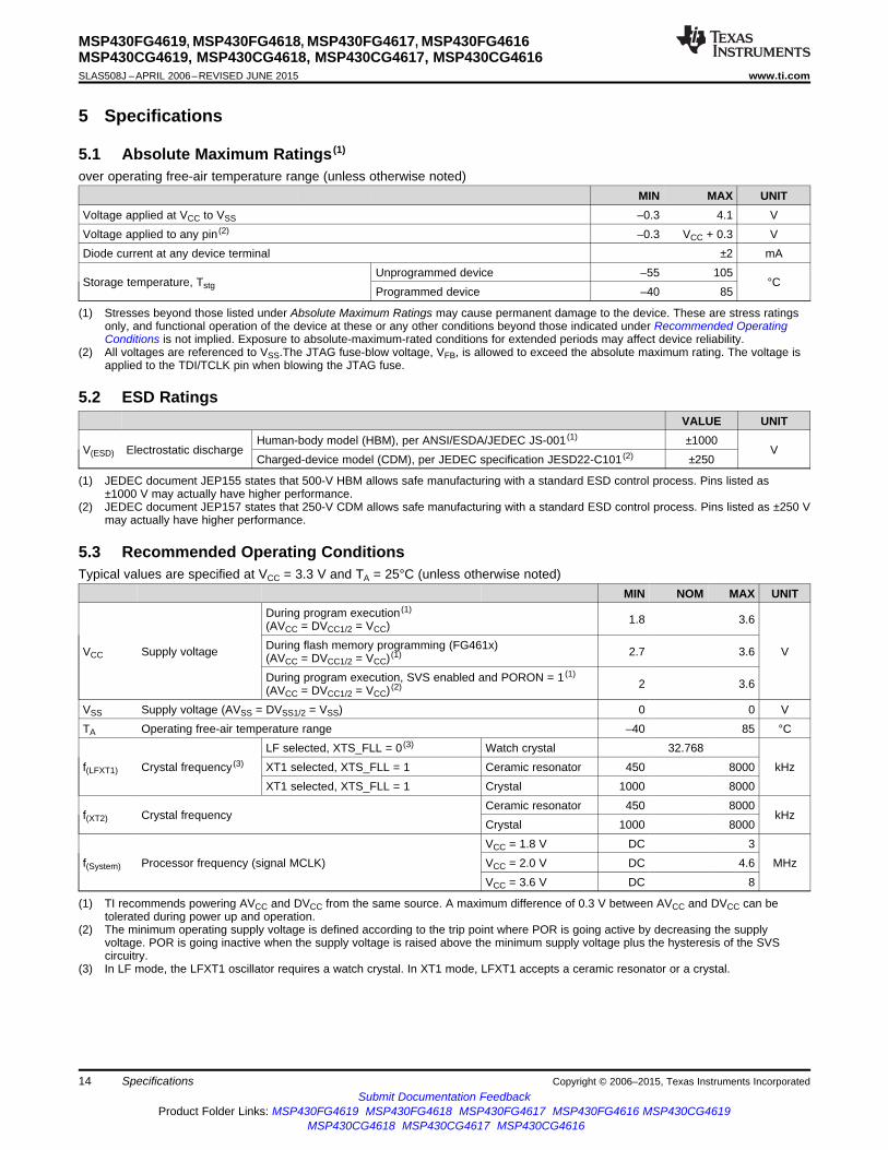
5.1 Absolute Maximum Ratings (1)
over operating free-air temperature range (unless otherwise noted)MIN MAX UNIT
Voltage applied at VCC to VSS –0.3 4.1 VVoltage applied to any pin (2) –0.3 VCC + 0.3 VDiode current at any device terminal ±2 mA
Unprogrammed device –55 105Storage temperature, Tstg °C
Programmed device –40 85
(1) Stresses beyond those listed under Absolute Maximum Ratings may cause permanent damage to the device. These are stress ratingsonly, and functional operation of the device at these or any other conditions beyond those indicated under Recommended OperatingConditions is not implied. Exposure to absolute-maximum-rated conditions for extended periods may affect device reliability.
(2) All voltages are referenced to VSS.The JTAG fuse-blow voltage, VFB, is allowed to exceed the absolute maximum rating. The voltage isapplied to the TDI/TCLK pin when blowing the JTAG fuse.
5.2 ESD RatingsVALUE UNIT
Human-body model (HBM), per ANSI/ESDA/JEDEC JS-001 (1) ±1000V(ESD) Electrostatic discharge V
Charged-device model (CDM), per JEDEC specification JESD22-C101 (2) ±250
(1) JEDEC document JEP155 states that 500-V HBM allows safe manufacturing with a standard ESD control process. Pins listed as±1000 V may actually have higher performance.
(2) JEDEC document JEP157 states that 250-V CDM allows safe manufacturing with a standard ESD control process. Pins listed as ±250 Vmay actually have higher performance.
5.3 Recommended Operating ConditionsTypical values are specified at VCC = 3.3 V and TA = 25°C (unless otherwise noted)
MIN NOM MAX UNITDuring program execution (1)
1.8 3.6(AVCC = DVCC1/2 = VCC)During flash memory programming (FG461x)VCC Supply voltage 2.7 3.6 V(AVCC = DVCC1/2 = VCC)(1)
During program execution, SVS enabled and PORON = 1 (1)2 3.6(AVCC = DVCC1/2 = VCC) (2)
VSS Supply voltage (AVSS = DVSS1/2 = VSS) 0 0 VTA Operating free-air temperature range –40 85 °C
LF selected, XTS_FLL = 0 (3) Watch crystal 32.768f(LFXT1) Crystal frequency (3) XT1 selected, XTS_FLL = 1 Ceramic resonator 450 8000 kHz
XT1 selected, XTS_FLL = 1 Crystal 1000 8000Ceramic resonator 450 8000
f(XT2) Crystal frequency kHzCrystal 1000 8000VCC = 1.8 V DC 3
f(System) Processor frequency (signal MCLK) VCC = 2.0 V DC 4.6 MHzVCC = 3.6 V DC 8
(1) TI recommends powering AVCC and DVCC from the same source. A maximum difference of 0.3 V between AVCC and DVCC can betolerated during power up and operation.
(2) The minimum operating supply voltage is defined according to the trip point where POR is going active by decreasing the supplyvoltage. POR is going inactive when the supply voltage is raised above the minimum supply voltage plus the hysteresis of the SVScircuitry.
(3) In LF mode, the LFXT1 oscillator requires a watch crystal. In XT1 mode, LFXT1 accepts a ceramic resonator or a crystal.
14 Specifications Copyright © 2006–2015, Texas Instruments IncorporatedSubmit Documentation Feedback
Product Folder Links: MSP430FG4619 MSP430FG4618 MSP430FG4617 MSP430FG4616 MSP430CG4619MSP430CG4618 MSP430CG4617 MSP430CG4616

1.8 3.62.7 3
3.0 MHz
8.0 MHz
Supply Voltage (V)
Supply voltage range, MSP430FG461x,
during flash memory programming
Supply voltage range,
MSP430xG461x, during
program execution
2.0
4.6 MHz
f (MHz)System
MSP430FG4619, MSP430FG4618, MSP430FG4617, MSP430FG4616MSP430CG4619, MSP430CG4618, MSP430CG4617, MSP430CG4616
www.ti.com SLAS508J –APRIL 2006–REVISED JUNE 2015
Figure 5-1. Frequency vs Supply Voltage
Copyright © 2006–2015, Texas Instruments Incorporated Specifications 15Submit Documentation Feedback
Product Folder Links: MSP430FG4619 MSP430FG4618 MSP430FG4617 MSP430FG4616 MSP430CG4619MSP430CG4618 MSP430CG4617 MSP430CG4616

MSP430FG4619, MSP430FG4618, MSP430FG4617, MSP430FG4616MSP430CG4619, MSP430CG4618, MSP430CG4617, MSP430CG4616SLAS508J –APRIL 2006–REVISED JUNE 2015 www.ti.com
5.4 Supply Current Into AVCC + DVCC Excluding External Currentover recommended ranges of supply voltage and operating free-air temperature (unless otherwise noted)
PARAMETER TEST CONDITION MIN TYP MAX UNITVCC = 2.2 V 280 370Active mode (1) (2)
CG461x TA = –40°C to 85°Cf(MCLK) = f(SMCLK) = 1 MHz, VCC = 3 V 470 580I(AM) f(ACLK) = 32768 Hz, µA
VCC = 2.2 V 400 480XTS = 0, SELM = (0, 1), FG461x TA = –40°C to 85°C(FG461x: program executes from flash) VCC = 3 V 600 740VCC = 2.2 V 45 70
I(LPM0) Low power mode (LPM0) (1) (2) TA = –40°C to 85°C µAVCC = 3 V 75 110
Low-power mode (LPM2), VCC = 2.2 V 11 20I(LPM2) f(MCLK) = f(SMCLK) = 0 MHz, TA = –40°C to 85°C µA
VCC = 3 V 17 24f(ACLK) = 32768 Hz, SCG0 = 0 (3) (2)
TA = –40°C 1.3 4.0TA = 25°C 1.3 4.0
VCC = 2.2 VLow-power mode (LPM3), TA = 60°C 2.22 6.5f(MCLK) = f(SMCLK) = 0 MHz,
TA = 85°C 6.5 15.0f(ACLK) = 32768 Hz, SCG0 = 1,I(LPM3) µABasic Timer1 enabled, ACLK selected, TA = –40°C 1.9 5.0LCD_A enabled, LCDCPEN = 0,
TA = 25°C 1.9 5.0(static mode, fLCD = f(ACLK)/32)(3) (4) (2)VCC = 3 V
TA = 60°C 2.5 7.5TA = 85°C 7.5 18.0TA = –40°C 1.5 5.5TA = 25°C 1.5 5.5
VCC = 2.2 VLow-power mode (LPM3), TA = 60°C 2.8 7.0f(MCLK) = f(SMCLK) = 0 MHz,
TA = 85°C 7.2 17.0f(ACLK) = 32768 Hz, SCG0 = 1,I(LPM3) µABasic Timer1 enabled, ACLK selected, TA = –40°C 2.5 6.5LCD_A enabled, LCDCPEN = 0,
TA = 25°C 2.5 6.5(4-mux mode; fLCD = f(ACLK)/32)(3) (4) (2)VCC = 3 V
TA = 60°C 3.2 8.0TA = 85°C 8.5 20.0TA = –40°C 0.13 1.0TA = 25°C 0.22 1.0
VCC = 2.2 VTA = 60°C 0.9 2.5
Low-power mode (LPM4), TA = 85°C 4.3 12.5I(LPM4) f(MCLK) = 0 MHz, f(SMCLK) = 0 MHz, µA
TA = –40°C 0.13 1.6f(ACLK) = 0 Hz, SCG0 = 1 (3) (2)
TA = 25°C 0.3 1.6VCC = 3 V
TA = 60°C 1.1 3.0TA = 85°C 5.0 15.0
(1) Timer_B is clocked by f(DCOCLK) = f(DCO) = 1 MHz. All inputs are tied to 0 V or to VCC. Outputs do not source or sink any current.(2) Current for brownout included.(3) All inputs are tied to 0 V or to VCC. Outputs do not source or sink any current.(4) The LPM3 currents are characterized with a Micro Crystal CC4V-T1A (9 pF) crystal and OSCCAPx = 1h.
Current consumption of active mode versus system frequency, FG version:
I(AM) = I(AM) [1 MHz] × f(System) [MHz]
Current consumption of active mode versus supply voltage, FG version:
I(AM) = I(AM) [3 V] + 200 µA/V × (VCC – 3 V)
16 Specifications Copyright © 2006–2015, Texas Instruments IncorporatedSubmit Documentation Feedback
Product Folder Links: MSP430FG4619 MSP430FG4618 MSP430FG4617 MSP430FG4616 MSP430CG4619MSP430CG4618 MSP430CG4617 MSP430CG4616
MSP430FG4619, MSP430FG4618, MSP430FG4617, MSP430FG4616MSP430CG4619, MSP430CG4618, MSP430CG4617, MSP430CG4616
www.ti.com SLAS508J –APRIL 2006–REVISED JUNE 2015
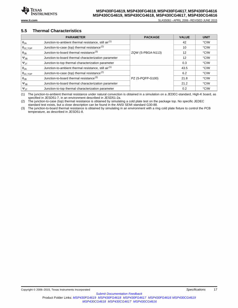
5.5 Thermal CharacteristicsPARAMETER PACKAGE VALUE UNIT
θJA Junction-to-ambient thermal resistance, still air (1) 42 °C/WθJC,TOP Junction-to-case (top) thermal resistance (2) 10 °C/WθJB Junction-to-board thermal resistance (3) ZQW (S-PBGA-N113) 12 °C/WΨJB Junction-to-board thermal characterization parameter 12 °C/WΨJT Junction-to-top thermal characterization parameter 0.3 °C/WθJA Junction-to-ambient thermal resistance, still air (1) 43.5 °C/WθJC,TOP Junction-to-case (top) thermal resistance (2) 6.2 °C/WθJB Junction-to-board thermal resistance (3) PZ (S-PQFP-G100) 21.8 °C/WΨJB Junction-to-board thermal characterization parameter 21.2 °C/WΨJT Junction-to-top thermal characterization parameter 0.2 °C/W
(1) The junction-to-ambient thermal resistance under natural convection is obtained in a simulation on a JEDEC-standard, High-K board, asspecified in JESD51-7, in an environment described in JESD51-2a.
(2) The junction-to-case (top) thermal resistance is obtained by simulating a cold plate test on the package top. No specific JEDECstandard test exists, but a close description can be found in the ANSI SEMI standard G30-88.
(3) The junction-to-board thermal resistance is obtained by simulating in an environment with a ring cold plate fixture to control the PCBtemperature, as described in JESD51-8.
Copyright © 2006–2015, Texas Instruments Incorporated Specifications 17Submit Documentation Feedback
Product Folder Links: MSP430FG4619 MSP430FG4618 MSP430FG4617 MSP430FG4616 MSP430CG4619MSP430CG4618 MSP430CG4617 MSP430CG4616
MSP430FG4619, MSP430FG4618, MSP430FG4617, MSP430FG4616MSP430CG4619, MSP430CG4618, MSP430CG4617, MSP430CG4616SLAS508J –APRIL 2006–REVISED JUNE 2015 www.ti.com
5.6 Schmitt-Trigger Inputs – Ports P1 to P10, RST/NMI, JTAG (TCK, TMS, TDI/TCLK,TDO/TDI)over recommended ranges of supply voltage and operating free-air temperature (unless otherwise noted)
PARAMETER TEST CONDITIONS MIN MAX UNITVCC = 2.2 V 1.1 1.55
VIT+ Positive-going input threshold voltage VVCC = 3 V 1.5 1.98VCC = 2.2 V 0.4 0.9
VIT– Negative-going input threshold voltage VVCC = 3 V 0.9 1.3VCC = 2.2 V 0.3 1.1
Vhys Input voltage hysteresis (VIT+ – VIT– ) VVCC = 3 V 0.5 1
5.7 Inputs Px.x, TAx, TBXover recommended ranges of supply voltage and operating free-air temperature (unless otherwise noted)
PARAMETER TEST CONDITIONS VCC MIN MAX UNIT2.2 V 62Port P1, P2: P1.x to P2.x, external trigger signalt(int) External interrupt timing nsfor the interrupt flag (1) 3 V 502.2 V 62TA0, TA1, TA2t(cap) Timer_A, Timer_B capture timing nsTB0, TB1, TB2, TB3, TB4, TB5, TB6 3 V 50
f(TAext) 2.2 V 8Timer_A or Timer_B clock frequency TACLK, TBCLK MHzexternally applied to pin INCLK t(H) = t(L)f(TBext) 3 V 10f(TAint) 2.2 V 8
Timer A or Timer B clock frequency SMCLK or ACLK signal selected MHzf(TBint) 3 V 10
(1) The external signal sets the interrupt flag every time the minimum t(int) parameters are met. It may be set even with trigger signalsshorter than t(int).
5.8 Leakage Current – Ports P1 to P10 (1)
over recommended ranges of supply voltage and operating free-air temperature (unless otherwise noted)PARAMETER TEST CONDITIONS MIN MAX UNIT
V(Px.y) (2)Ilkg(Px.y) Leakage current, Port Px VCC = 2.2 V, 3 V ±50 nA(1 ≤ × ≤ 10, 0 ≤ y ≤ 7)
(1) The leakage current is measured with VSS or VCC applied to the corresponding pins, unless otherwise noted.(2) The port pin must be selected as input.
5.9 Outputs – Ports P1 to P10over recommended ranges of supply voltage and operating free-air temperature (unless otherwise noted)
PARAMETER TEST CONDITIONS MIN MAX UNITIOH(max) = –1.5 mA, VCC = 2.2 V (1) VCC – 0.25 VCC
IOH(max) = –6 mA, VCC = 2.2 V (2) VCC – 0.6 VCCVOH High-level output voltage VIOH(max) = –1.5 mA, VCC = 3 V (1) VCC – 0.25 VCC
IOH(max) = –6 mA, VCC = 3 V (2) VCC – 0.6 VCC
IOL(max) = 1.5 mA, VCC = 2.2 V (1) VSS VSS + 0.25IOL(max) = 6 mA, VCC = 2.2 V (2) VSS VSS + 0.6
VOL Low-level output voltage VIOL(max) = 1.5 mA, VCC = 3 V (1) VSS VSS + 0.25IOL(max) = 6 mA, VCC = 3 V (2) VSS VSS + 0.6
(1) The maximum total current, IOH(max) and IOL(max), for all outputs combined, should not exceed ±12 mA to satisfy the maximum specifiedvoltage drop.
(2) The maximum total current, IOH(max) and IOL(max), for all outputs combined, should not exceed ±48 mA to satisfy the maximum specifiedvoltage drop.
18 Specifications Copyright © 2006–2015, Texas Instruments IncorporatedSubmit Documentation Feedback
Product Folder Links: MSP430FG4619 MSP430FG4618 MSP430FG4617 MSP430FG4616 MSP430CG4619MSP430CG4618 MSP430CG4617 MSP430CG4616

MSP430FG4619, MSP430FG4618, MSP430FG4617, MSP430FG4616MSP430CG4619, MSP430CG4618, MSP430CG4617, MSP430CG4616
www.ti.com SLAS508J –APRIL 2006–REVISED JUNE 2015
5.10 Output Frequencyover recommended ranges of supply voltage and operating free-air temperature (unless otherwise noted)
PARAMETER TEST CONDITIONS MIN TYP MAX UNITVCC = 2.2 V DC 10
f(Px.y) (1 ≤ × ≤ 10, 0 ≤ y ≤ 7) CL = 20 F, IL = ±1.5 mA MHzVCC = 3 V DC 12
f(MCLK) P1.1/TA0/MCLK VCC = 2.2 V 10f(SMCLK) P1.4/TBCLK/SMCLK CL = 20 pF MHzf(ACLK) P1.5/TACLK/ACLK VCC = 3 V DC 12
f(ACLK) = f(LFXT1) = f(XT1) 40% 60%P1.5/TACLK/ACLK, f(ACLK) = f(LFXT1) = f(LF) 30% 70%CL = 20 pF, VCC = 2.2 V, 3 V
f(ACLK) = f(LFXT1) 50%f(MCLK) = f(XT1) 40% 60%Duty cycle of output P1.1/TA0/MCLK,t(Xdc) 50% – 50%+frequency CL = 20 pF, VCC = 2.2 V, 3 V f(MCLK) = f(DCOCLK) 50%15 ns 15 nsf(SMCLK) = f(XT2) 40% 60%
P1.4/TBCLK/SMCLK,50% – 50% +CL = 20 pF, VCC = 2.2 V, 3 V f(SMCLK) = f(DCOCLK) 50%15 ns 15 ns
Copyright © 2006–2015, Texas Instruments Incorporated Specifications 19Submit Documentation Feedback
Product Folder Links: MSP430FG4619 MSP430FG4618 MSP430FG4617 MSP430FG4616 MSP430CG4619MSP430CG4618 MSP430CG4617 MSP430CG4616

!
0.0
-5.0
-10.0
-15.0
-20.0
-25.00.0 0.5 1.0 1.5 2.0 2.5
T = 25 CA °
T = 85 CA °
V = 2.2 V
P2.0CC
V High-Level Output Voltage VOH - -
I-
typ
ica
l H
igh
-Le
ve
l O
utp
ut
Cu
rre
nt
- m
AO
H
0.0
-10.0
-20.0
-30.0
-40.0
-50.0
ITy
pic
al
Hig
h-L
ev
el
Ou
tpu
t C
urr
en
mA
OH
--
0.0 0.5 1.0 1.5 2.0 2.5 3.0 3.5
V High-Level Output Voltage VOH - -
T = 25 CA °
T = 85 CA °
V = 3 V
P2.0CC
25.0
20.0
15.0
10.0
5.0
0.00.0 0.5 1.0 1.5 2.0 2.5
V Low-Level Output Voltage VOL – –
V = 2.2 V
P2.0CC T = 25 CA °
T = 85 CA °
I-
Ty
pic
al
Lo
w-L
ev
el
Ou
tpu
t C
urr
en
t -
mA
OL
50.0
40.0
30.0
20.0
10.0
0.00.0 0.5 1.0 1.5 2.0 2.5 3.0 3.5
V Low-Level Output Voltage VOL - -
ITyp
ical L
ow
-Level O
utp
ut
Cu
rren
tm
AO
L-
-
V = 3 V
P2.0CC
T = 25 CA °
T = 85 CA °
MSP430FG4619, MSP430FG4618, MSP430FG4617, MSP430FG4616MSP430CG4619, MSP430CG4618, MSP430CG4617, MSP430CG4616SLAS508J –APRIL 2006–REVISED JUNE 2015 www.ti.com
5.11 Typical Characteristics – Outputsover recommended ranges of supply voltage and operating free-air temperature (unless otherwise noted)
Figure 5-2. Typical Low-Level Output Current vs Typical Low- Figure 5-3. Typical Low-Level Output Current vs Typical Low-Level Output Current Level Output Current
Figure 5-4. Typical High-Level Output Current vs Typical High- Figure 5-5. Typical High-Level Output Current vs Typical High-Level Output Current Level Output Current
20 Specifications Copyright © 2006–2015, Texas Instruments IncorporatedSubmit Documentation Feedback
Product Folder Links: MSP430FG4619 MSP430FG4618 MSP430FG4617 MSP430FG4616 MSP430CG4619MSP430CG4618 MSP430CG4617 MSP430CG4616

MSP430FG4619, MSP430FG4618, MSP430FG4617, MSP430FG4616MSP430CG4619, MSP430CG4618, MSP430CG4617, MSP430CG4616
www.ti.com SLAS508J –APRIL 2006–REVISED JUNE 2015
5.12 Wake-up Timing From LPM3over recommended ranges of supply voltage and operating free-air temperature (unless otherwise noted)
PARAMETER TEST CONDITIONS MIN MAX UNITf = 1 MHz 6
td(LPM3) Delay time f = 2 MHz VCC = 2.2 V, 3 V 6 µsf = 3 MHz 6
5.13 RAMover recommended ranges of supply voltage and operating free-air temperature (unless otherwise noted)
PARAMETER TEST CONDITIONS MIN MAX UNITVRAMh CPU halted (1) 1.6 V
(1) This parameter defines the minimum supply voltage when the data in program memory RAM remain unchanged. No program executionshould take place during this supply voltage condition.
5.14 LCD_Aover recommended ranges of supply voltage and operating free-air temperature (unless otherwise noted)
PARAMETER TEST CONDITIONS VCC MIN TYP MAX UNITCharge pump enabledVCC(LCD) Supply voltage (1) 2.2 3.6 V(LCDCPEN = 1, VLCDx > 0000)VLCD(typ) = 3 V, LCDCPEN = 1,
ICC(LCD) Supply current (1) VLCDx= 1000, all segments on, fLCD = fACLK/32, 2.2 V 3 µAno LCD connected (2), TA = 25°CCharge pump enabledCLCD Capacitor on LCDCAP (3) (4) 4.7 µF(LCDCPEN = 1, VLCDx > 0000)
fLCD LCD frequency 1.1 kHzVLCDx = 0000 VCC
VLCDx = 0001 2.60VLCDx = 0010 2.66VLCDx = 0011 2.72VLCDx = 0100 2.78VLCDx = 0101 2.84VLCDx = 0110 2.90VLCDx = 0111 2.96
VLCD LCD voltage (4) VVLCDx = 1000 3.02VLCDx = 1001 3.08VLCDx = 1010 3.14VLCDx = 1011 3.20VLCDx = 1100 3.26VLCDx = 1101 3.32VLCDx = 1110 3.38VLCDx = 1111 3.44 3.60
RLCD VLCD= 3 V, CPEN = 1,LCD driver output impedance 2.2 V 10 kΩVLCDx = 1000, ILOAD = ±10 µΑ
(1) Refer to the supply current specifications I(LPM3) for additional current specifications with the LCD_A module active.(2) Connecting an actual display increases the current consumption depending on the size of the LCD.(3) Enabling the internal charge pump with an external capacitor smaller than the minimum specified might damage the device.(4) Segments S0 through S3 are disabled when the LCD charge pump feature is enabled (LCDCPEN = 1) and, therefore, cannot be used
together with the LCD charge pump. On the MSP430xG461x devices only, S0 through S3 are also disabled if VLCDEXT = 1. Thissetting is typically used to apply an external LCD voltage supply to the LCDCAP terminal. For these devices, set LCDCPEN = 0,VLCDEXT = 0, and VLCDx > 0 to enable an external LCD voltage supply to be applied to the LCDCAP terminal.
Copyright © 2006–2015, Texas Instruments Incorporated Specifications 21Submit Documentation Feedback
Product Folder Links: MSP430FG4619 MSP430FG4618 MSP430FG4617 MSP430FG4616 MSP430CG4619MSP430CG4618 MSP430CG4617 MSP430CG4616

Voltage @ 0.5 V nodeCC
VCC
Voltage @ 0.25 V nodeCC
VCC
MSP430FG4619, MSP430FG4618, MSP430FG4617, MSP430FG4616MSP430CG4619, MSP430CG4618, MSP430CG4617, MSP430CG4616SLAS508J –APRIL 2006–REVISED JUNE 2015 www.ti.com
5.15 Comparator_A (1)
over recommended ranges of supply voltage and operating free-air temperature (unless otherwise noted)PARAMETER TEST CONDITIONS VCC MIN TYP MAX UNIT
2.2 V 25 40I(CC) CAON = 1, CARSEL = 0, CAREF = 0 µA
3 V 45 602.2 V 30 50CAON = 1, CARSEL = 0, CAREF = (1, 2, 3),I(Refladder/RefDiode) µANo load at P1.6/CA0 and P1.7/CA1 3 V 45 71
PCA0 = 1, CARSEL = 1, CAREF = 1,V(Ref025) 2.2 V, 3 V 0.23 0.24 0.25No load at P1.6/CA0 and P1.7/CA1PCA0 = 1, CARSEL = 1, CAREF = 2,V(Ref050) 2.2 V, 3 V 0.47 0.48 0.5No load at P1.6/CA0 and P1.7/CA1PCA0 = 1, CARSEL = 1, CAREF = 3, 2.2 V 390 480 540
V(RefVT) No load at P1.6/CA0 and P1.7/CA1, mV3 V 400 490 550TA = 85°C
Common-mode inputVIC CAON = 1 2.2 V, 3 V 0 VCC – 1 Vvoltage rangeVp – VS Offset voltage (2) 2.2 V, 3 V –30 30 mVVhys Input hysteresis CAON = 1 2.2 V, 3 V 0 0.7 1.4 mV
2.2 V 160 210 300TA = 25°C, nsOverdrive 10 mV, without filter: CAF = 0 3 V 80 150 240t(response LH) 2.2 V 1.4 1.9 3.4TA = 25°C, µsOverdrive 10 mV, without filter: CAF = 1 3 V 0.9 1.5 2.6t(response HL) 2.2 V 130 210 300TA = 25°C, nsOverdrive 10 mV, without filter: CAF = 0 3 V 80 150 240
2.2 V 1.4 1.9 3.4TA = 25°C, µsOverdrive 10 mV, without filter: CAF = 1 3 V 0.9 1.5 2.6
(1) The leakage current for the Comparator_A terminals is identical to Ilkg(Px.x) specification.(2) The input offset voltage can be cancelled by using the CAEX bit to invert the Comparator_A inputs on successive measurements. The
two successive measurements are then summed together.
22 Specifications Copyright © 2006–2015, Texas Instruments IncorporatedSubmit Documentation Feedback
Product Folder Links: MSP430FG4619 MSP430FG4618 MSP430FG4617 MSP430FG4616 MSP430CG4619MSP430CG4618 MSP430CG4617 MSP430CG4616

Overdrive VCAOUT
t(response)V+
V-
400 mV
_
+
CAON
0
1
V+0
1
CAF
Low-Pass Filter
t » 2 µ s
To Internal
Modules
Set CAIFG
Flag
CAOUT
V-
VCC
1
0 V
0
650
600
550
500
450
400-45 -25 -5 15 35 55 75 95
T Free-Air Temperature CA - - °
VR
efe
ren
ce
Vo
lta
ge
mV
RE
F-
-
V = 3 VCC
Typical
650
600
550
500
450
400-45 -25 -5 15 35 55 75 95
T Free-Air Temperature CA - - °
VR
efe
ren
ce V
olt
ag
em
VR
EF
--
V = 2.2 VCC
Typical
MSP430FG4619, MSP430FG4618, MSP430FG4617, MSP430FG4616MSP430CG4619, MSP430CG4618, MSP430CG4617, MSP430CG4616
www.ti.com SLAS508J –APRIL 2006–REVISED JUNE 2015
5.16 Typical Characteristics – Comparator_A
Figure 5-6. Reference Voltage vs Free-Air Temperature Figure 5-7. Reference Voltage vs Free-Air Temperature
Figure 5-8. Block Diagram of Comparator_A Module
Figure 5-9. Overdrive Definition
Copyright © 2006–2015, Texas Instruments Incorporated Specifications 23Submit Documentation Feedback
Product Folder Links: MSP430FG4619 MSP430FG4618 MSP430FG4617 MSP430FG4616 MSP430CG4619MSP430CG4618 MSP430CG4617 MSP430CG4616

VCC(drop)
VCC
3 V
tpw
0
0.5
1
1.5
2
0.001 1 1000
Typical Conditions
1 ns 1 nst - Pulse Width -pw ms t - Pulse Width -pw ms
V = 3 VCC
V-
VC
C(d
rop
)
0
1
td(BOR)
VCC
V(B_IT-)
Vhys(B_IT-)
VCC(start)
MSP430FG4619, MSP430FG4618, MSP430FG4617, MSP430FG4616MSP430CG4619, MSP430CG4618, MSP430CG4617, MSP430CG4616SLAS508J –APRIL 2006–REVISED JUNE 2015 www.ti.com
5.17 POR, BORover recommended ranges of supply voltage and operating free-air temperature (unless otherwise noted) (1)
PARAMETER TEST CONDITIONS MIN TYP MAX UNITtd(BOR) 2000 µs
0.7 ×VCC(start) dVCC/dt ≤ 3 V/s (see Figure 5-10) VV(B_IT– )
dVCC/dt ≤ 3 V/s (see Figure 5-10 through Figure 5-V(B_IT–) Brownout (2) (3) 1.79 V12)Vhys(B_IT–) dVCC/dt ≤ 3 V/s (see Figure 5-10) 70 130 210 mV
Pulse duration needed at RST/NMI pin to acceptedt(reset) 2 µsreset internally, VCC = 2.2 V, 3 V
(1) The current consumption of the brownout module is already included in the ICC current consumption data.(2) The voltage level V(B_IT–) + Vhys(B_IT–) ≤ 1.89 V.(3) During power up, the CPU begins code execution following a period of td(BOR) after VCC = V(B_IT–) + Vhys(B_IT–). The default FLL+ settings
must not be changed until VCC ≥ VCC(min), where VCC(min) is the minimum supply voltage for the desired operating frequency. See theMSP430x4xx Family User’s Guide (SLAU056) for more information on the brownout and SVS circuit.
Figure 5-10. POR, BOR vs Supply Voltage
Figure 5-11. VCC(drop) Level with a Square Voltage Drop to Generate a POR or BOR Signal
24 Specifications Copyright © 2006–2015, Texas Instruments IncorporatedSubmit Documentation Feedback
Product Folder Links: MSP430FG4619 MSP430FG4618 MSP430FG4617 MSP430FG4616 MSP430CG4619MSP430CG4618 MSP430CG4617 MSP430CG4616

VCC
0
0.5
1
1.5
2
VCC(drop)
tpw
tpw - Pulse Width - ms
VC
C(d
rop
)-
V
3 V
0.001 1 1000 tf tr
tpw - Pulse Width - ms
t = tf r
Typical Conditions
V = 3 VCC
MSP430FG4619, MSP430FG4618, MSP430FG4617, MSP430FG4616MSP430CG4619, MSP430CG4618, MSP430CG4617, MSP430CG4616
www.ti.com SLAS508J –APRIL 2006–REVISED JUNE 2015
Figure 5-12. VCC(drop) Level With a Triangle Voltage Drop to Generate a POR or BOR Signal
5.18 SVS (Supply Voltage Supervisor and Monitor)over recommended ranges of supply voltage and operating free-air temperature (unless otherwise noted)
PARAMETER TEST CONDITIONS MIN TYP MAX UNITdVCC/dt > 30 V/ms (see Figure 5-13) 5 150
t(SVSR) µsdVCC/dt ≤ 30 V/ms 2000
td(SVSon) SVS on, switch from VLD = 0 to VLD ≠ 0, VCC = 3 V 150 300 µstsettle VLD ≠ 0 (1) 12 µsV(SVSstart) VLD ≠ 0, VCC/dt ≤ 3 V/s (see Figure 5-13) 1.55 1.7 V
VLD = 1 70 120 155 mVVCC/dt ≤ 3 V/s (see Figure 5-13) V(SVS_IT–) V(SVS_IT–)VLD = 2 to 14Vhys(SVS_IT–) × 0.001 × 0.016VCC/dt ≤ 3 V/s (see Figure 5-13), external voltage VLD = 15 4.4 20 mVapplied on A7
VLD = 1 1.8 1.9 2.05VLD = 2 1.94 2.1 2.23VLD = 3 2.05 2.2 2.35VLD = 4 2.14 2.3 2.46VLD = 5 2.24 2.4 2.58VLD = 6 2.33 2.5 2.69VLD = 7 2.46 2.65 2.84
VCC/dt ≤ 3 V/s (see Figure 5-13)VLD = 8 2.58 2.8 2.97V(SVS_IT–) VVLD = 9 2.69 2.9 3.10VLD = 10 2.83 3.05 3.26VLD = 11 2.94 3.2 3.39VLD = 12 3.11 3.35 3.58 (2)
VLD = 13 3.24 3.5 3.73 (2)
VLD = 14 3.43 3.7 (2) 3.96 (2)
VCC/dt ≤ 3 V/s (see Figure 5-13), external voltage VLD = 15 1.1 1.2 1.3applied on A7ICC(SVS)
(3) VLD ≠ 0, VCC = 2.2 V, 3 V 10 15 µA
(1) tsettle is the settling time that the comparator output needs to have a stable level after VLD is switched from VLD ≠ 0 to a different VLDvalue from 2 to 15. The overdrive is assumed to be > 50 mV.
(2) The recommended operating voltage range is limited to 3.6 V.(3) The current consumption of the SVS module is not included in the ICC current consumption data.
Copyright © 2006–2015, Texas Instruments Incorporated Specifications 25Submit Documentation Feedback
Product Folder Links: MSP430FG4619 MSP430FG4618 MSP430FG4617 MSP430FG4616 MSP430CG4619MSP430CG4618 MSP430CG4617 MSP430CG4616

0
0.5
1
1.5
2
VCC
VCC
1 ns 1 ns
tpw
tpw - Pulse Width - ms
3 V
1 10 1000
tf tr
t - Pulse Width - ms
100
tpw
3 V
t = tf r
Rectangular Drop
Triangular Drop
VCC(drop)
VC
C(d
rop
)-
V
VCC(drop)
VCC(start)
VCC
V(B_IT-)
BrownoutRegion
V(SVSstart)
V(SVS_IT-)
Software Sets VLD>0:
SVS is Active
td(SVSR)
undefined
Vhys(SVS_IT-)
0
1
td(BOR)
Brownout
0
1
td(SVSon)
td(BOR)
0
1
Set POR
BrownOut
Region
SVS Circuit is Active From VLD > to VCC < V(B_IT-)SVSOut
Vhys(B_IT-)
MSP430FG4619, MSP430FG4618, MSP430FG4617, MSP430FG4616MSP430CG4619, MSP430CG4618, MSP430CG4617, MSP430CG4616SLAS508J –APRIL 2006–REVISED JUNE 2015 www.ti.com
Figure 5-13. SVS Reset (SVSR) vs Supply Voltage
Figure 5-14. VCC(drop) with a Square Voltage Drop and a Triangle Voltage Drop to Generate an SVS Signal
26 Specifications Copyright © 2006–2015, Texas Instruments IncorporatedSubmit Documentation Feedback
Product Folder Links: MSP430FG4619 MSP430FG4618 MSP430FG4617 MSP430FG4616 MSP430CG4619MSP430CG4618 MSP430CG4617 MSP430CG4616
T -A °CV - VCC
1.8 3.02.4 3.6
1.0
20 6040 85
1.0
0-20-400
f(DCO)
f(DCO3V)
f(DCO)
f(DCO20 C)°
MSP430FG4619, MSP430FG4618, MSP430FG4617, MSP430FG4616MSP430CG4619, MSP430CG4618, MSP430CG4617, MSP430CG4616
www.ti.com SLAS508J –APRIL 2006–REVISED JUNE 2015
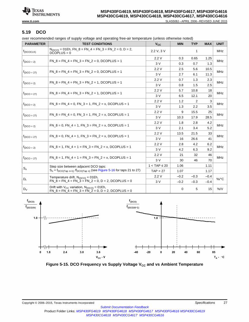
5.19 DCOover recommended ranges of supply voltage and operating free-air temperature (unless otherwise noted)
PARAMETER TEST CONDITIONS VCC MIN TYP MAX UNITN(DCO) = 01Eh, FN_8 = FN_4 = FN_3 = FN_2 = 0, D = 2,f(DCOCLK) 2.2 V, 3 V 1 MHzDCOPLUS = 0
2.2 V 0.3 0.65 1.25f(DCO = 2) FN_8 = FN_4 = FN_3 = FN_2 = 0, DCOPLUS = 1 MHz
3 V 0.3 0.7 1.32.2 V 2.5 5.6 10.5
f(DCO = 27) FN_8 = FN_4 = FN_3 = FN_2 = 0, DCOPLUS = 1 MHz3 V 2.7 6.1 11.3
2.2 V 0.7 1.3 2.3f(DCO = 2) FN_8 = FN_4 = FN_3 = FN_2 = 1, DCOPLUS = 1 MHz
3 V 0.8 1.5 2.52.2 V 5.7 10.8 18
f(DCO = 27) FN_8 = FN_4 = FN_3 = FN_2 = 1, DCOPLUS = 1 MHz3 V 6.5 12.1 20
2.2 V 1.2 2 3f(DCO = 2) FN_8 = FN_4 = 0, FN_3 = 1, FN_2 = x, DCOPLUS = 1 MHz
3 V 1.3 2.2 3.52.2 V 9 15.5 25
f(DCO = 27) FN_8 = FN_4 = 0, FN_3 = 1, FN_2 = x, DCOPLUS = 1 MHz3 V 10.3 17.9 28.5
2.2 V 1.8 2.8 4.2f(DCO = 2) FN_8 = 0, FN_4 = 1, FN_3 = FN_2 = x, DCOPLUS = 1 MHz
3 V 2.1 3.4 5.22.2 V 13.5 21.5 33
f(DCO = 27) FN_8 = 0, FN_4 = 1, FN_3 = FN_2 = x, DCOPLUS = 1 MHz3 V 16 26.6 41
2.2 V 2.8 4.2 6.2f(DCO = 2) FN_8 = 1, FN_4 = 1 = FN_3 = FN_2 = x, DCOPLUS = 1 MHz
3 V 4.2 6.3 9.22.2 V 21 32 46
f(DCO = 27) FN_8 = 1, FN_4 = 1 = FN_3 = FN_2 = x, DCOPLUS = 1 MHz3 V 30 46 70
1 < TAP ≤ 20 1.06 1.11Step size between adjacent DCO taps:Sn Sn = fDCO(Tap n+1) /fDCO(Tap n) (see Figure 5-16 for taps 21 to 27) TAP = 27 1.07 1.172.2 V –0.2 –0.3 –0.4Temperature drift, N(DCO) = 01Eh,Dt %/°CFN_8 = FN_4 = FN_3 = FN_2 = 0, D = 2, DCOPLUS = 0 3 V –0.2 –0.3 –0.4
Drift with VCC variation, N(DCO) = 01Eh,DV 0 5 15 %/VFN_8 = FN_4 = FN_3 = FN_2 = 0, D = 2, DCOPLUS = 0
Figure 5-15. DCO Frequency vs Supply Voltage VCC and vs Ambient Temperature
Copyright © 2006–2015, Texas Instruments Incorporated Specifications 27Submit Documentation Feedback
Product Folder Links: MSP430FG4619 MSP430FG4618 MSP430FG4617 MSP430FG4616 MSP430CG4619MSP430CG4618 MSP430CG4617 MSP430CG4616

DCO Frequency
Adjusted by Bits
2 to 2 in SCFI1 N 9 5
DCO
FN_2=0
FN_3=0
FN_4=0
FN_8=0
FN_2=1
FN_3=0
FN_4=0
FN_8=0
FN_2=x
FN_3=1
FN_4=0
FN_8=0
FN_2=x
FN_3=x
FN_4=1
FN_8=0
FN_2=x
FN_3=x
FN_4=x
FN_8=1
Legend
Tolerance at Tap 27
Tolerance at Tap 2
Overlapping DCO Ranges:
Uninterrupted Frequency Range
f (D
CO
)
1 2720
1.11
1.17
DCO Tap
Sn
-S
tep
siz
eR
ati
ob
etw
ee
nD
CO
Ta
ps
Min
Max
1.07
1.06
MSP430FG4619, MSP430FG4618, MSP430FG4617, MSP430FG4616MSP430CG4619, MSP430CG4618, MSP430CG4617, MSP430CG4616SLAS508J –APRIL 2006–REVISED JUNE 2015 www.ti.com
Figure 5-16. DCO Tap Step Size
Figure 5-17. Five Overlapping DCO Ranges Controlled by FN_x Bits
28 Specifications Copyright © 2006–2015, Texas Instruments IncorporatedSubmit Documentation Feedback
Product Folder Links: MSP430FG4619 MSP430FG4618 MSP430FG4617 MSP430FG4616 MSP430CG4619MSP430CG4618 MSP430CG4617 MSP430CG4616
MSP430FG4619, MSP430FG4618, MSP430FG4617, MSP430FG4616MSP430CG4619, MSP430CG4618, MSP430CG4617, MSP430CG4616
www.ti.com SLAS508J –APRIL 2006–REVISED JUNE 2015
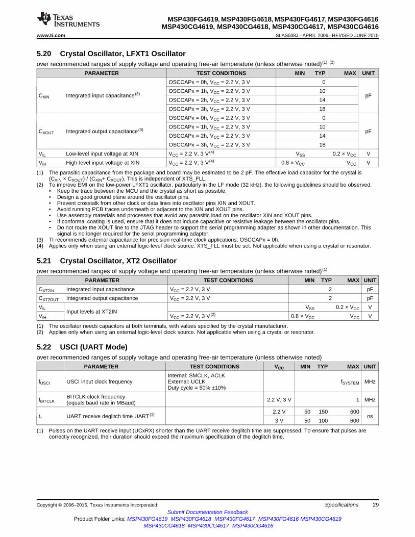
5.20 Crystal Oscillator, LFXT1 Oscillatorover recommended ranges of supply voltage and operating free-air temperature (unless otherwise noted) (1) (2)
PARAMETER TEST CONDITIONS MIN TYP MAX UNITOSCCAPx = 0h, VCC = 2.2 V, 3 V 0OSCCAPx = 1h, VCC = 2.2 V, 3 V 10
CXIN Integrated input capacitance (3) pFOSCCAPx = 2h, VCC = 2.2 V, 3 V 14OSCCAPx = 3h, VCC = 2.2 V, 3 V 18OSCCAPx = 0h, VCC = 2.2 V, 3 V 0OSCCAPx = 1h, VCC = 2.2 V, 3 V 10
CXOUT Integrated output capacitance (3) pFOSCCAPx = 2h, VCC = 2.2 V, 3 V 14OSCCAPx = 3h, VCC = 2.2 V, 3 V 18
VIL Low-level input voltage at XIN VCC = 2.2 V, 3 V (4) VSS 0.2 × VCC VVIH High-level input voltage at XIN VCC = 2.2 V, 3 V (4) 0.8 × VCC VCC V
(1) The parasitic capacitance from the package and board may be estimated to be 2 pF. The effective load capacitor for the crystal is(CXIN × CXOUT) / (CXIN+ CXOUT). This is independent of XTS_FLL.
(2) To improve EMI on the low-power LFXT1 oscillator, particularly in the LF mode (32 kHz), the following guidelines should be observed.• Keep the trace between the MCU and the crystal as short as possible.• Design a good ground plane around the oscillator pins.• Prevent crosstalk from other clock or data lines into oscillator pins XIN and XOUT.• Avoid running PCB traces underneath or adjacent to the XIN and XOUT pins.• Use assembly materials and processes that avoid any parasitic load on the oscillator XIN and XOUT pins.• If conformal coating is used, ensure that it does not induce capacitive or resistive leakage between the oscillator pins.• Do not route the XOUT line to the JTAG header to support the serial programming adapter as shown in other documentation. This
signal is no longer required for the serial programming adapter.(3) TI recommends external capacitance for precision real-time clock applications; OSCCAPx = 0h.(4) Applies only when using an external logic-level clock source. XTS_FLL must be set. Not applicable when using a crystal or resonator.
5.21 Crystal Oscillator, XT2 Oscillatorover recommended ranges of supply voltage and operating free-air temperature (unless otherwise noted) (1)
PARAMETER TEST CONDITIONS MIN TYP MAX UNITCXT2IN Integrated input capacitance VCC = 2.2 V, 3 V 2 pFCXT2OUT Integrated output capacitance VCC = 2.2 V, 3 V 2 pFVIL VSS 0.2 × VCC V
Input levels at XT2INVIH VCC = 2.2 V, 3 V (2) 0.8 × VCC VCC V
(1) The oscillator needs capacitors at both terminals, with values specified by the crystal manufacturer.(2) Applies only when using an external logic-level clock source. Not applicable when using a crystal or resonator.
5.22 USCI (UART Mode)over recommended ranges of supply voltage and operating free-air temperature (unless otherwise noted)
PARAMETER TEST CONDITIONS VCC MIN TYP MAX UNITInternal: SMCLK, ACLK
fUSCI USCI input clock frequency External: UCLK fSYSTEM MHzDuty cycle = 50% ±10%
BITCLK clock frequencyfBITCLK 2.2 V, 3 V 1 MHz(equals baud rate in MBaud)2.2 V 50 150 600
tτ UART receive deglitch time UART (1) ns3 V 50 100 600
(1) Pulses on the UART receive input (UCxRX) shorter than the UART receive deglitch time are suppressed. To ensure that pulses arecorrectly recognized, their duration should exceed the maximum specification of the deglitch time.
Copyright © 2006–2015, Texas Instruments Incorporated Specifications 29Submit Documentation Feedback
Product Folder Links: MSP430FG4619 MSP430FG4618 MSP430FG4617 MSP430FG4616 MSP430CG4619MSP430CG4618 MSP430CG4617 MSP430CG4616

MSP430FG4619, MSP430FG4618, MSP430FG4617, MSP430FG4616MSP430CG4619, MSP430CG4618, MSP430CG4617, MSP430CG4616SLAS508J –APRIL 2006–REVISED JUNE 2015 www.ti.com
5.23 USCI (SPI Master Mode)over recommended ranges of supply voltage and operating free-air temperature (unless otherwise noted) (see Figure 5-18and Figure 5-19)
PARAMETER TEST CONDITIONS VCC MIN MAX UNITSMCLK, ACLKfUSCI USCI input clock frequency fSYSTEM MHzDuty cycle = 50% ±10%
2.2 V 110tSU,MI SOMI input data setup time ns
3 V 752.2 V 0
tHD,MI iSOMI input data hold time ns3 V 0
2.2 V 30tVALID,MO SIMO output data valid time UCLK edge to SIMO valid, CL = 20 pF ns
3 V 20
5.24 USCI (SPI Slave Mode)over recommended ranges of supply voltage and operating free-air temperature (unless otherwise noted) (see Figure 5-20and Figure 5-21)
PARAMETER TEST CONDITIONS VCC MIN TYP MAX UNITSTE lead timetSTE,LEAD 2.2 V, 3 V 50 nsSTE low to clockSTE lag timetSTE,LAG 2.2 V, 3 V 10 nsLast clock to STE highSTE access timetSTE,ACC 2.2 V, 3 V 50 nsSTE low to SOMI data outSTE disable timetSTE,DIS 2.2 V, 3 V 50 nsSTE high to SOMI high impedance
2.2 V 20tSU,SI SIMO input data setup time ns
3 V 152.2 V 10
tHD,SI SIMO input data hold time ns3 V 10
2.2 V 75 110tVALID,SO SOMI output data valid time UCLK edge to SOMI valid, CL = 20 pF ns
3 V 50 75
30 Specifications Copyright © 2006–2015, Texas Instruments IncorporatedSubmit Documentation Feedback
Product Folder Links: MSP430FG4619 MSP430FG4618 MSP430FG4617 MSP430FG4616 MSP430CG4619MSP430CG4618 MSP430CG4617 MSP430CG4616

UCLK
CKPL = 0
CKPL = 1
SIMO
1/fUC xC LK
tLOW /HIGH tLOW /HIGH
SOMI
tSU ,MI
tHD ,MI
tVALID ,MO
UCLK
CKPL = 0
CKPL = 1
SIMO
1/fUCx CLK
tLOW /HIGH tLOW /HIGH
SOMI
tSU ,MI
tHD ,MI
tVALID ,MO
MSP430FG4619, MSP430FG4618, MSP430FG4617, MSP430FG4616MSP430CG4619, MSP430CG4618, MSP430CG4617, MSP430CG4616
www.ti.com SLAS508J –APRIL 2006–REVISED JUNE 2015
Figure 5-18. SPI Master Mode, CKPH = 0
Figure 5-19. SPI Master Mode, CKPH = 1
Copyright © 2006–2015, Texas Instruments Incorporated Specifications 31Submit Documentation Feedback
Product Folder Links: MSP430FG4619 MSP430FG4618 MSP430FG4617 MSP430FG4616 MSP430CG4619MSP430CG4618 MSP430CG4617 MSP430CG4616

STE
UCLK
CKPL =0
CKPL =1
tSTE ,LEAD tSTE ,LAG
tACC tDIS
tLOW /HIGH tLOW /HIGH
tSU ,SI
tHD ,SI
tVALID ,SO
SO MI
SIMO
1/fUCx CLK
STE
UCLK
CKPL = 0
CKPL = 1
SOMI
tACC tDIS
1/fUCx CLK
tLOW /HIGH tLOW /HIGH
SIMO
tSU ,SIMO
tHD ,SIMO
tVALID ,SOMI
tSTE ,LEAD tSTE ,LAG
MSP430FG4619, MSP430FG4618, MSP430FG4617, MSP430FG4616MSP430CG4619, MSP430CG4618, MSP430CG4617, MSP430CG4616SLAS508J –APRIL 2006–REVISED JUNE 2015 www.ti.com
Figure 5-20. SPI Slave Mode, CKPH = 0
Figure 5-21. SPI Slave Mode, CKPH = 1
32 Specifications Copyright © 2006–2015, Texas Instruments IncorporatedSubmit Documentation Feedback
Product Folder Links: MSP430FG4619 MSP430FG4618 MSP430FG4617 MSP430FG4616 MSP430CG4619MSP430CG4618 MSP430CG4617 MSP430CG4616

SDA
SCL
tLOW
tHD , DAT
tSU , DAT
tHD , STA tSU , STA tHD , STA
tHIGH
tSU , STO
tSP
tBUF
MSP430FG4619, MSP430FG4618, MSP430FG4617, MSP430FG4616MSP430CG4619, MSP430CG4618, MSP430CG4617, MSP430CG4616
www.ti.com SLAS508J –APRIL 2006–REVISED JUNE 2015
5.25 USCI (I2C Mode)over recommended ranges of supply voltage and operating free-air temperature (unless otherwise noted) (see Figure 5-22)
PARAMETER TEST CONDITIONS VCC MIN TYP MAX UNITInternal: SMCLK, ACLK
fUSCI USCI input clock frequency External: UCLK fSYSTEM MHzDuty Cycle = 50% ±10%
fSCL SCL clock frequency 2.2 V, 3 V 0 400 kHzfSCL ≤ 100 kHz 2.2 V, 3 V 4
tHD,STA Hold time (repeated) START µsfSCL > 100 kHz 2.2 V, 3 V 0.6fSCL ≤ 100 kHz 2.2 V, 3 V 4.7
tSU,STA Setup time for a repeated START µsfSCL > 100 kHz 2.2 V, 3 V 0.6
tHD,DAT Data hold time 2.2 V, 3 V 0 nstSU,DAT Data setup time 2.2 V, 3 V 250 nstSU,STO Setup time for STOP 2.2 V, 3 V 4 µs
2.2 V 50 150 600Pulse duration of spikes suppressed bytSP nsinput filter 3 V 50 100 600
Figure 5-22. I2C Mode Timing
5.26 USART1over recommended ranges of supply voltage and operating free-air temperature (unless otherwise noted) (1)
PARAMETER TEST CONDITIONS MIN TYP MAX UNITVCC = 2.2 V, SYNC = 0, UART mode 200 430 800
t(τ) USART1 deglitch time nsVCC = 3 V, SYNC = 0, UART mode 150 280 500
(1) The signal applied to the USART1 receive signal (terminal) (URXD1) must meet the timing requirements of t(τ) to ensure that the URXSflip-flop is set. The URXS flip-flop is set with negative pulses that meet the minimum-timing condition of t(τ). The operating conditions toset the flag must be met independently from this timing constraint. The deglitch circuitry is active only on negative transitions on theURXD1 line.
Copyright © 2006–2015, Texas Instruments Incorporated Specifications 33Submit Documentation Feedback
Product Folder Links: MSP430FG4619 MSP430FG4618 MSP430FG4617 MSP430FG4616 MSP430CG4619MSP430CG4618 MSP430CG4617 MSP430CG4616

MSP430FG4619, MSP430FG4618, MSP430FG4617, MSP430FG4616MSP430CG4619, MSP430CG4618, MSP430CG4617, MSP430CG4616SLAS508J –APRIL 2006–REVISED JUNE 2015 www.ti.com
5.27 12-Bit ADC, Power Supply and Input Range Conditionsover recommended ranges of supply voltage and operating free-air temperature (unless otherwise noted) (1)
PARAMETER TEST CONDITIONS MIN TYP MAX UNITAVCC and DVCC are connected together,
AVCC Analog supply voltage AVSS and DVSS are connected together, 2.2 3.6 VV(AVSS) = V(DVSS) = 0 VAll external Ax terminals, Analog inputs selected in
V(P6.x/Ax) Analog input voltage range (2) ADC12MCTLx register, P6Sel.x = 1, 0 VAVCC VV(AVSS) ≤ VAx ≤ V(AVCC)
fADC12CLK = 5.0 MHz, VCC = 2.2 V 0.65 1.3Operating supply current intoIADC12 ADC12ON = 1, REFON = 0, mAAVCC terminal (3) VCC = 3 V 0.8 1.6SHT0 = 0, SHT1 = 0, ADC12DIV = 0fADC12CLK = 5.0 MHz, VCC = 3 V 0.5 0.8ADC12ON = 0, REFON = 1, REF2_5V = 1Operating supply current intoIREF+ mAAVCC terminal (4) VCC = 2.2 V 0.5 0.8fADC12CLK = 5.0 MHz,ADC12ON = 0, REFON = 1, REF2_5V = 0 VCC = 3 V 0.5 0.8Only one terminal can be selected at oneCI Input capacitance VCC = 2.2 V 40 pFtime, Ax
RI Input MUX ON resistance 0 V ≤ VAx ≤ VAVCC VCC = 3 V 2000 Ω
(1) The leakage current is defined in the leakage current table with Ax parameter.(2) The analog input voltage range must be within the selected reference voltage range VR+ to VR– for valid conversion results.(3) The internal reference supply current is not included in current consumption parameter IADC12.(4) The internal reference current is supplied from terminal AVCC. Consumption is independent of the ADC12ON control bit, unless a
conversion is active. The REFON bit enables to settle the built-in reference before starting an A/D conversion.
5.28 12-Bit ADC, External Referenceover recommended ranges of supply voltage and operating free-air temperature (unless otherwise noted) (1)
PARAMETER TEST CONDITIONS MIN TYP MAX UNITPositive external referenceVeREF+ VeREF+ > VREF–/VeREF–
(2) 1.4 VAVCC Vvoltage inputNegative external referenceVREF–/VeREF– VeREF+ > VREF–/VeREF–
(3) 0 1.2 Vvoltage input(VeREF+ – Differential external reference VeREF+ > VREF–/VeREF–
(4) 1.4 VAVCC VVREF–/VeREF–) voltage inputIVeREF+ Input leakage current 0 V ≤ VeREF+ ≤ VAVCC VCC = 2.2 V, 3 V ±1 µAIVREF–/VeREF– Input leakage current 0 V ≤ VeREF– ≤ VAVCC VCC = 2.2 V, 3 V ±1 µA
(1) The external reference is used during conversion to charge and discharge the capacitance array. The input capacitance, CI, is also thedynamic load for an external reference during conversion. The dynamic impedance of the reference supply should follow therecommendations on analog-source impedance to allow the charge to settle for 12-bit accuracy.
(2) The accuracy limits the minimum positive external reference voltage. Lower reference voltage levels may be applied with reducedaccuracy requirements.
(3) The accuracy limits the maximum negative external reference voltage. Higher reference voltage levels may be applied with reducedaccuracy requirements.
(4) The accuracy limits minimum external differential reference voltage. Lower differential reference voltage levels may be applied withreduced accuracy requirements.
34 Specifications Copyright © 2006–2015, Texas Instruments IncorporatedSubmit Documentation Feedback
Product Folder Links: MSP430FG4619 MSP430FG4618 MSP430FG4617 MSP430FG4616 MSP430CG4619MSP430CG4618 MSP430CG4617 MSP430CG4616
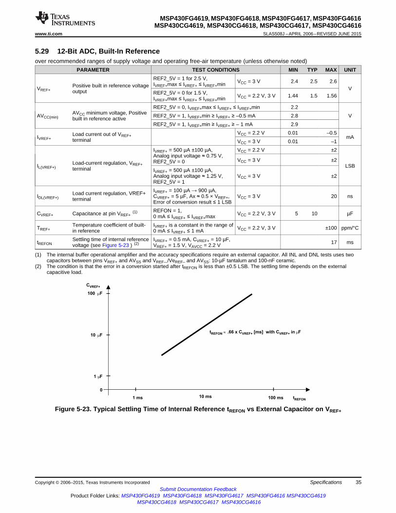
CVREF+
1 mF
0
1 ms 10 ms 100 ms tREFON
tREFON » .66 x C [ms] with C inVREF+ VREF+ mF
100 mF
10 mF
MSP430FG4619, MSP430FG4618, MSP430FG4617, MSP430FG4616MSP430CG4619, MSP430CG4618, MSP430CG4617, MSP430CG4616
www.ti.com SLAS508J –APRIL 2006–REVISED JUNE 2015
5.29 12-Bit ADC, Built-In Referenceover recommended ranges of supply voltage and operating free-air temperature (unless otherwise noted)
PARAMETER TEST CONDITIONS MIN TYP MAX UNITREF2_5V = 1 for 2.5 V, VCC = 3 V 2.4 2.5 2.6IVREF+max ≤ IVREF+ ≤ IVREF+minPositive built in reference voltageVREF+ Voutput REF2_5V = 0 for 1.5 V, VCC = 2.2 V, 3 V 1.44 1.5 1.56IVREF+max ≤ IVREF+ ≤ IVREF+minREF2_5V = 0, IVREF+max ≤ IVREF+ ≤ IVREF+min 2.2
AVCC minimum voltage, PositiveAVCC(min) REF2_5V = 1, IVREF+min ≥ IVREF+ ≥ –0.5 mA 2.8 Vbuilt in reference activeREF2_5V = 1, IVREF+min ≥ IVREF+ ≥ – 1 mA 2.9
VCC = 2.2 V 0.01 –0.5Load current out of VREF+IVREF+ mAterminal VCC = 3 V 0.01 –1IVREF+ = 500 µA ±100 µA, VCC = 2.2 V ±2Analog input voltage ≈ 0.75 V,
VCC = 3 V ±2REF2_5V = 0Load-current regulation, VREF+IL(VREF+) LSBterminal IVREF+ = 500 µA ±100 µA,Analog input voltage ≈ 1.25 V, VCC = 3 V ±2REF2_5V = 1IVREF+ = 100 µA → 900 µA,Load current regulation, VREF+IDL(VREF+) CVREF+ = 5 µF, Ax ≈ 0.5 × VREF+, VCC = 3 V 20 nsterminal Error of conversion result ≤ 1 LSBREFON = 1,CVREF+ Capacitance at pin VREF+
(1) VCC = 2.2 V, 3 V 5 10 µF0 mA ≤ IVREF+ ≤ IVREF+maxTemperature coefficient of built- IVREF+ is a constant in the range ofTREF+ VCC = 2.2 V, 3 V ±100 ppm/°Cin reference 0 mA ≤ IVREF+ ≤ 1 mASettling time of internal reference IVREF+ = 0.5 mA, CVREF+ = 10 µF,tREFON 17 msvoltage (see Figure 5-23 ) (2) VREF+ = 1.5 V, VAVCC = 2.2 V
(1) The internal buffer operational amplifier and the accuracy specifications require an external capacitor. All INL and DNL tests uses twocapacitors between pins VREF+ and AVSS and VREF-–/VeREF– and AVSS: 10-µF tantalum and 100-nF ceramic.
(2) The condition is that the error in a conversion started after tREFON is less than ±0.5 LSB. The settling time depends on the externalcapacitive load.
Figure 5-23. Typical Settling Time of Internal Reference tREFON vs External Capacitor on VREF+
Copyright © 2006–2015, Texas Instruments Incorporated Specifications 35Submit Documentation Feedback
Product Folder Links: MSP430FG4619 MSP430FG4618 MSP430FG4617 MSP430FG4616 MSP430CG4619MSP430CG4618 MSP430CG4617 MSP430CG4616

+
-
10 mF 100 nF
AVSS
MSP430FG461x
+
-
10 mF 100 nF
AVCC
10 mF 100 nF
DVSS1/2
DVCC1/2From
Power
Supply
+
-
Apply External Reference [V ]eREF+
or Use Internal Reference [V ]REF+V or VREF+ eREF+
V /VREF- eREF-Reference Is Internally
Switched to AVSS
+
-
10 mF 100 nF
AVSS
MSP430FG461x
+
-
+
-
10 mF 100 nF
10 mF 100 nF
AVCC
10 m F 100 nF
DVSS1/2
DVCC1/2From
Power
Supply
Apply
External
Reference
+
-
Apply External Reference [V ]eREF+
or Use Internal Reference [V ]REF+V or VREF+ eREF+
V /VREF- eREF-
MSP430FG4619, MSP430FG4618, MSP430FG4617, MSP430FG4616MSP430CG4619, MSP430CG4618, MSP430CG4617, MSP430CG4616SLAS508J –APRIL 2006–REVISED JUNE 2015 www.ti.com
Figure 5-24. Supply Voltage and Reference Voltage Design VREF–/VeREF– External Supply
Figure 5-25. Supply Voltage and Reference Voltage Design VREF–/VeREF– = AVSS, Internally Connected
36 Specifications Copyright © 2006–2015, Texas Instruments IncorporatedSubmit Documentation Feedback
Product Folder Links: MSP430FG4619 MSP430FG4618 MSP430FG4617 MSP430FG4616 MSP430CG4619MSP430CG4618 MSP430CG4617 MSP430CG4616

MSP430FG4619, MSP430FG4618, MSP430FG4617, MSP430FG4616MSP430CG4619, MSP430CG4618, MSP430CG4617, MSP430CG4616
www.ti.com SLAS508J –APRIL 2006–REVISED JUNE 2015
5.30 12-Bit ADC, Timing Parametersover recommended ranges of supply voltage and operating free-air temperature (unless otherwise noted)
PARAMETER TEST CONDITIONS VCC MIN TYP MAX UNITFor specified performance of ADC12fADC12CLK 2.2 V, 3 V 0.45 5 6.3 MHzlinearity parameters
Internal ADC12 ADC12DIV = 0,fADC12OSC 2.2 V, 3 V 3.7 5 6.3 MHzoscillator fADC12CLK = fADC12OSC
CVREF+ ≥ 5 µF, Internal oscillator, 2.2 V, 3 V 2.06 3.51fADC12OSC = 3.7 MHz to 6.3 MHztCONVERT Conversion time µsExternal fADC12CLK from ACLK, MCLK, or 13 × ADC12DIVSMCLK, × 1/fADC12CLKADC12SSEL ≠ 0
Turnon settling timetADC12ON(1) 100 nsof the ADC
3 V 1220RS = 400 Ω,RI = 1000 Ω,tSample Sampling time nsCI = 30pF, τ = [RS +RI] × CI(2) 2.2 V 1400
(1) The condition is that the error in a conversion started after tADC12ON is less than ±0.5 LSB. The reference and input signal are alreadysettled.
(2) Approximately ten Tau (τ) are needed to get an error of less than ±0.5 LSB:tSample = ln(2n+1) × (RS + RI) x CI+ 800 ns where n = ADC resolution = 12, RS = external source resistance.
5.31 12-Bit ADC, Linearity Parametersover recommended ranges of supply voltage and operating free-air temperature (unless otherwise noted)
PARAMETER TEST CONDITIONS VCC MIN TYP MAX UNIT1.4 V ≤ (VeREF+ – VREF–/VeREF–) min ≤ 1.6 V ±2Integral linearityEI 2.2 V, 3 V LSBerror 1.6 V < (VeREF+ – VREF–/VeREF–) min ≤ [VAVCC] ±1.7
Differential linearity (VeREF+ – VREF–/VeREF–) min ≤ (VeREF+ – VREF–/VeREF–),ED 2.2 V, 3 V ±1 LSBerror CVREF+ = 10 µF (tantalum) and 100 nF (ceramic)(VeREF+ – VREF–/VeREF–) min ≤ (VeREF+ – VREF–/VeREF–),
EO Offset error Internal impedance of source RS < 100 Ω, 2.2 V, 3 V ±2 ±4 LSBCVREF+ = 10 µF (tantalum) and 100 nF (ceramic)(VeREF+ – VREF–/VeREF–)min ≤ (VeREF+ – VREF–/VeREF–),EG Gain error 2.2 V, 3 V ±1.1 ±2 LSBCVREF+ = 10 µF (tantalum) and 100 nF (ceramic)
Total unadjusted (VeREF+ -– VREF–/VeREF– )min ≤ (VeREF+ –VREF–/VeREF–),ET 2.2 V, 3 V ±2 ±5 LSBerror CVREF+ = 10 µF (tantalum) and 100 nF (ceramic)
Copyright © 2006–2015, Texas Instruments Incorporated Specifications 37Submit Documentation Feedback
Product Folder Links: MSP430FG4619 MSP430FG4618 MSP430FG4617 MSP430FG4616 MSP430CG4619MSP430CG4618 MSP430CG4617 MSP430CG4616
MSP430FG4619, MSP430FG4618, MSP430FG4617, MSP430FG4616MSP430CG4619, MSP430CG4618, MSP430CG4617, MSP430CG4616SLAS508J –APRIL 2006–REVISED JUNE 2015 www.ti.com
5.32 12-Bit ADC, Temperature Sensor and Built-In VMID
over recommended ranges of supply voltage and operating free-air temperature (unless otherwise noted)PARAMETER TEST CONDITIONS VCC MIN TYP MAX UNIT
2.2 V 40 120Operating supply current REFON = 0, INCH = 0Ah,ISENSOR µAinto AVCC terminal (1) ADC12ON = N/A, TA = 25°C 3 V 60 160ADC12ON = 1, INCH = 0Ah,VSENSOR
(2) 2.2 V, 3 V 986 mVTA = 0°CTCSENSOR ADC12ON = 1, INCH = 0Ah 2.2 V, 3 V 3.55 ±3% mV/°C
2.2 V 30Sample time required if ADC12ON = 1, INCH = 0Ah,tSENSOR(sample) µschannel 10 is selected (3) Error of conversion result ≤ 1 LSB 3 V 302.2 V N/A (4)Current into divider atIVMID ADC12ON = 1, INCH = 0Bh µAchannel 11 (4) 3 V N/A (4)
2.2 V 1.1 1.1 ±0.04ADC12ON = 1, INCH = 0Bh,VMID AVCC divider at channel 11 VVMID ≈ 0.5 × VAVCC 3 V 1.5 1.50 ±0.042.2 V 1400Sample time required if ADC12ON = 1, INCH = 0Bh,tVMID(sample) nschannel 11 is selected (5) Error of conversion result ≤ 1 LSB 3 V 1220
(1) The sensor current ISENSOR is consumed if (ADC12ON = 1 and REFON = 1), or (ADC12ON = 1 AND INCH = 0Ah and sample signal ishigh). When REFON = 1, ISENSOR is already included in IREF+.
(2) The temperature sensor offset can be as much as ±20°C. TI recommends a single-point calibration to minimize the offset error of thebuilt-in temperature sensor.
(3) The typical equivalent impedance of the sensor is 51 kΩ. The sample time required includes the sensor-on time tSENSOR(on)(4) No additional current is needed. The VMID is used during sampling.(5) The on-time tVMID(on) is included in the sampling time tVMID(sample); no additional on time is needed.
5.33 12-Bit DAC, Supply Specificationsover recommended ranges of supply voltage and operating free-air temperature (unless otherwise noted)
PARAMETER TEST CONDITIONS VCC MIN TYP MAX UNITAVCC Analog supply voltage AVCC = DVCC, AVSS = DVSS = 0 V 2.20 3.60 V
DAC12AMPx = 2, DAC12IR = 0, 50 110DAC12_xDAT = 0800hDAC12AMPx = 2, DAC12IR = 1,DAC12_xDAT = 0800h, 50 110VeREF+ = VREF+ = AVCCSupply current, single DACIDD 2.2 V, 3 V µADAC12AMPx = 5, DAC12IR = 1,channel (1) (2)DAC12_xDAT = 0800h, 200 440VeREF+ = VREF+ = AVCC
DAC12AMPx = 7, DAC12IR = 1,DAC12_xDAT = 0800h, 700 1500VeREF+ = VREF+ = AVCC
DAC12_xDAT = 800h, VREF = 1.5 V, 2.2 VΔAVCC = 100 mVPower-supply rejectionPSRR 70 dBratio (3) (4) DAC12_×DAT = 800h, VREF = 1.5 V or 2.5 V, 3 VΔAVCC = 100 mV
(1) No load at the output pin, DAC12_0 or DAC12_1, assuming that the control bits for the shared pins are set properly.(2) Current into reference terminals not included. If DAC12IR = 1 current flows through the input divider; see Reference Input specifications.(3) PSRR = 20 × logΔAVCC/ΔVDAC12_xOUT.(4) VREF is applied externally. The internal reference is not used.
38 Specifications Copyright © 2006–2015, Texas Instruments IncorporatedSubmit Documentation Feedback
Product Folder Links: MSP430FG4619 MSP430FG4618 MSP430FG4617 MSP430FG4616 MSP430CG4619MSP430CG4618 MSP430CG4617 MSP430CG4616

Positive
Negative
VR+
Gain ErrorOffset Error
DAC Code
DAC VOUT
Ideal transfer
function
RLoad =
AVCC
CLoad = 100pF
2
DAC Output
MSP430FG4619, MSP430FG4618, MSP430FG4617, MSP430FG4616MSP430CG4619, MSP430CG4618, MSP430CG4617, MSP430CG4616
www.ti.com SLAS508J –APRIL 2006–REVISED JUNE 2015
5.34 12-Bit DAC, Linearity Specificationsover recommended ranges of supply voltage and operating free-air temperature (unless otherwise noted) (see Figure 5-26)
PARAMETER TEST CONDITIONS VCC MIN TYP MAX UNITResolution 12-bit monotonic 12 bits
Vref = 1.5 V, 2.2 VDAC12AMPx = 7, DAC12IR = 1INL Integral nonlinearity (1) ±2.0 ±8.0 LSB
Vref = 2.5 V, 3 VDAC12AMPx = 7, DAC12IR = 1Vref = 1.5 V, 2.2 VDAC12AMPx = 7, DAC12IR = 1
DNL Differential nonlinearity (1) ±0.4 ±1.0 LSBVref = 2.5 V, 3 VDAC12AMPx = 7, DAC12IR = 1Vref = 1.5 V, 2.2 VDAC12AMPx = 7, DAC12IR = 1
Offset voltage without calibration (1) (2) ±21Vref = 2.5 V, 3 VDAC12AMPx = 7, DAC12IR = 1
EO mVVref = 1.5 V, 2.2 VDAC12AMPx = 7, DAC12IR = 1
Offset voltage with calibration (1) (2) ±2.5Vref = 2.5 V, 3 VDAC12AMPx = 7, DAC12IR = 1
dE(O)/dT Offset error temperature coefficient (1) 2.2 V, 3 V ±30 µV/°CVREF = 1.5 V 2.2 V
EG Gain error (1) ±3.5 %FSRVREF = 2.5 V 3 V
ppm ofdE(G)/dT Gain temperature coefficient (1) 2.2 V, 3 V 10 FSR/°CDAC12AMPx = 2 100
tOffset_Cal Time for offset calibration (3) DAC12AMPx = 3, 5 2.2 V, 3 V 32 msDAC12AMPx = 4, 6, 7 6
(1) Parameters calculated from the best-fit curve from 0x0A to 0xFFF. The best-fit curve method is used to deliver coefficients “a” and “b” ofthe first order equation: y = a + b × x. VDAC12_xOUT = EO + (1 + EG) × (VeREF+/4095) × DAC12_xDAT, DAC12IR = 1.
(2) The offset calibration works on the output operational amplifier. Offset calibration is triggered by setting bit DAC12CALON.(3) The offset calibration can be done if DAC12AMPx = 2, 3, 4, 5, 6, 7. The output operational amplifier is switched off with DAC12AMPx =
0, 1. TI recommends that the DAC12 module be configured before initiating calibration. Port activity during calibration may effectaccuracy and is not recommended.
Figure 5-26. Linearity Test Load Conditions and Gain and Offset Definition
Copyright © 2006–2015, Texas Instruments Incorporated Specifications 39Submit Documentation Feedback
Product Folder Links: MSP430FG4619 MSP430FG4618 MSP430FG4617 MSP430FG4616 MSP430CG4619MSP430CG4618 MSP430CG4617 MSP430CG4616

DAC12_xDAT - Digital Code
DN
L-
Dif
fere
nti
al N
on
lin
eari
ty E
rro
r -
LS
B
2.0
1.5
1.0
0.5
0.0
-0.5
-1.0
-1.5
-2.0
0 512 1024 1536 2048 2560 3072 3584 4095
V = 2.2 V, V = 1/.5 V
DAC12AMPx = 7DAC12IR = 1
CC REF
V = 2.2 V, V = 1.5 V
DAC12AMPx = 7DAC12IR = 1
CC REF
4
3
2
1
0
-1
-2
-3
-4
0 512 1024 1536 2048 2560 3072 3584 4095
DAC12_xDAT – Digital Code
INL
–In
teg
ral N
on
lin
eari
ty E
rro
r–
LS
B
MSP430FG4619, MSP430FG4618, MSP430FG4617, MSP430FG4616MSP430CG4619, MSP430CG4618, MSP430CG4617, MSP430CG4616SLAS508J –APRIL 2006–REVISED JUNE 2015 www.ti.com
Figure 5-27. Typical INL Error vs Digital Input Data
Figure 5-28. Typical DNL Error vs Digital Input Data
40 Specifications Copyright © 2006–2015, Texas Instruments IncorporatedSubmit Documentation Feedback
Product Folder Links: MSP430FG4619 MSP430FG4618 MSP430FG4617 MSP430FG4616 MSP430CG4619MSP430CG4618 MSP430CG4617 MSP430CG4616

RO/P(DAC12_x)
Max
0.3
AVCC
AVCC -0.3V VOUT
Min
RLoad
AVCC
CLoad = 100pF
2
ILoad
DAC12
O/P(DAC12_x)
MSP430FG4619, MSP430FG4618, MSP430FG4617, MSP430FG4616MSP430CG4619, MSP430CG4618, MSP430CG4617, MSP430CG4616
www.ti.com SLAS508J –APRIL 2006–REVISED JUNE 2015
5.35 12-Bit DAC, Output Specificationsover recommended ranges of supply voltage and operating free-air temperature (unless otherwise noted)
PARAMETER TEST CONDITIONS VCC MIN TYP MAX UNITNo load, VeREF+ = AVCC,DAC12_xDAT = 0h, DAC12IR = 1, 0 0.005DAC12AMPx = 7No load, VeREF+ = AVCC, AVCC –DAC12_xDAT = 0FFFh, DAC12IR = 1, AVCC0.05DAC12AMPx = 7Output voltage range (seeVO 2.2 V, 3 V VFigure 5-29) (1) RLoad = 3 kΩ, VeREF+ = AVCC,DAC12_xDAT = 0h, DAC12IR = 1, 0 0.1DAC12AMPx = 7RLoad = 3 kΩ, VeREF+ = AVCC, AVCC –DAC12_xDAT = 0FFFh, DAC12IR = 1, AVCC0.13DAC12AMPx = 7
Max DAC12 loadCL(DAC12) 2.2 V, 3 V 100 pFcapacitance2.2 V –0.5 +0.5
IL(DAC12) Max DAC12 load current mA3 V –1.0 +1.0
RLoad = 3 kΩ, VO/P(DAC12) < 0.3 V, 150 250DAC12AMPx = 2, DAC12_xDAT = 0hRLoad = 3 kΩ,Output resistance (seeRO/P(DAC12) VO/P(DAC12) > AVCC – 0.3 V, 2.2 V, 3 V 150 250 ΩFigure 5-29) DAC12_xDAT = 0FFFhRLoad = 3 kΩ, 1 40.3 V ≤ VO/P(DAC12) ≤ AVCC – 0.3 V
(1) Data is valid after the offset calibration of the output amplifier.
Figure 5-29. DAC12_x Output Resistance Tests
5.36 12-Bit DAC, Reference Input Specificationsover recommended ranges of supply voltage and operating free-air temperature (unless otherwise noted)
PARAMETER TEST CONDITIONS VCC MIN TYP MAX UNITDAC12IR = 0 (1) (2) AVCC/3 AVCC + 0.2Reference input voltageVeREF+ 2.2 V, 3 V Vrange DAC12IR = 1 (3) (4) AVCC AVCC + 0.2DAC12_0 IR = DAC12_1 IR = 0 20 MΩDAC12_0 IR = 1, DAC12_1 IR = 0
40 48 56Ri(VREF+), DAC12_0 IR = 0, DAC12_1 IR = 1Reference input resistance 2.2 V, 3 V(Ri(VeREF+) kΩDAC12_0 IR = DAC12_1 IR = 1,DAC12_0 SREFx = DAC12_1 20 24 28SREFx (5)
(1) For a full-scale output, the reference input voltage can be as high as 1/3 of the maximum output voltage swing (AVCC).(2) The maximum voltage applied at reference input voltage terminal VeREF+ = [AVCC – VE(O)] / [3 × (1 + EG)].(3) For a full-scale output, the reference input voltage can be as high as the maximum output voltage swing (AVCC).(4) The maximum voltage applied at reference input voltage terminal VeREF+ = [AVCC – VE(O)] / (1 + EG).(5) When DAC12IR = 1 and DAC12SREFx = 0 or 1 for both channels, the reference input resistive dividers for each DAC are in parallel
reducing the reference input resistance.
Copyright © 2006–2015, Texas Instruments Incorporated Specifications 41Submit Documentation Feedback
Product Folder Links: MSP430FG4619 MSP430FG4618 MSP430FG4617 MSP430FG4616 MSP430CG4619MSP430CG4618 MSP430CG4617 MSP430CG4616
Conversion 1 Conversion 2
VOUT
Conversion 3
10%
tSRLH tSRHL
90%
10%
90%
RLoad
AVCC
CLoad = 100pF
2
DAC Output
RO/P(DAC12.x)
ILoad
Conversion 1 Conversion 2
VOUT
Conversion 3
Glitch
Energy
+/- 1/2 LSB
+/- 1/2 LSB
tsettleLH tsettleHL
= 3 k W
MSP430FG4619, MSP430FG4618, MSP430FG4617, MSP430FG4616MSP430CG4619, MSP430CG4618, MSP430CG4617, MSP430CG4616SLAS508J –APRIL 2006–REVISED JUNE 2015 www.ti.com
5.37 12-Bit DAC, Dynamic SpecificationsVref = VCC, DAC12IR = 1, over recommended ranges of supply voltage and operating free-air temperature (unless otherwisenoted) (see Figure 5-30 and Figure 5-31)
PARAMETER TEST CONDITIONS VCC MIN TYP MAX UNITDAC12AMPx = 0 → 2, 3, 4 60 120DAC12_xDAT = 800h,
tON DAC12 on time ErrorV(O) < ±0.5 LSB (1) DAC12AMPx = 0 → 5, 6 2.2 V, 3 V 15 30 µs(see Figure 5-30) DAC12AMPx = 0 → 7 6 12
DAC12AMPx = 2 100 200DAC12_xDAT =tS(FS) Settling time, full scale DAC12AMPx = 3,5 2.2 V, 3 V 40 80 µs80h→F7Fh→80h
DAC12AMPx = 4, 6, 7 15 30DAC12AMPx = 2 5DAC12_xDAT =
tS(C–C) Settling time, code to code 3F8h→408h→3F8h DAC12AMPx = 3,5 2.2 V, 3 V 2 µsBF8h→C08h→BF8h DAC12AMPx = 4, 6, 7 1
DAC12AMPx = 2 0.05 0.12DAC12_xDAT =SR Slew rate DAC12AMPx = 3,5 2.2 V, 3 V 0.35 0.7 V/µs80h→F7Fh→80h (2)
DAC12AMPx = 4, 6, 7 1.5 2.7DAC12AMPx = 2 600
DAC12_xDAT =Glitch energy, full-scale DAC12AMPx = 3,5 2.2 V, 3 V 150 nV-s80h→F7Fh→80hDAC12AMPx = 4, 6, 7 30
(1) RLoad and CLoad connected to AVSS (not AVCC/2) in Figure 5-30.(2) Slew rate applies to output voltage steps ≥ 200 mV.
Figure 5-30. Settling Time and Glitch Energy Testing
Figure 5-31. Slew Rate Testing
42 Specifications Copyright © 2006–2015, Texas Instruments IncorporatedSubmit Documentation Feedback
Product Folder Links: MSP430FG4619 MSP430FG4618 MSP430FG4617 MSP430FG4616 MSP430CG4619MSP430CG4618 MSP430CG4617 MSP430CG4616

DAC12_xDAT 080h
V OUT
1/fToggle
F7Fh
V DAC12_yOUT
080h F7Fh 080h
V DAC12_xOUT
REF+RLoad
AVCC
CLoad = 100 pF
2
ILoad
DAC12_1
RLoad
AVCC
CLoad = 100 pF
2
ILoad
DAC12_0
DAC0
DAC1
V
VeREF+
AC
DC
RLoad
AVCC
CLoad = 100pF
2
ILoad
DAC12_x
DACx
= 3 k W
MSP430FG4619, MSP430FG4618, MSP430FG4617, MSP430FG4616MSP430CG4619, MSP430CG4618, MSP430CG4617, MSP430CG4616
www.ti.com SLAS508J –APRIL 2006–REVISED JUNE 2015
5.38 12-Bit DAC, Dynamic Specifications ContinuedTA = 25°C (unless otherwise noted)
PARAMETER TEST CONDITIONS VCC MIN TYP MAX UNITDAC12AMPx = 2, 3, 4, DAC12SREFx = 2, 40DAC12IR = 1, DAC12_xDAT = 800h
3-dB bandwidth, DAC12AMPx = 5, 6, DAC12SREFx = 2,BW–3dB VDC = 1.5 V, VAC = 0.1 VPP 2.2 V, 3 V 180 kHzDAC12IR = 1, DAC12_xDAT = 800h(see Figure 5-32)DAC12AMPx = 7, DAC12SREFx = 2, 550DAC12IR = 1, DAC12_xDAT = 800hDAC12_0DAT = 800h, No Load,DAC12_1DAT = 80h↔F7Fh, RLoad = 3 kΩ –80
Channel-to-channel fDAC12_1OUT = 10 kHz at 50/50 duty cyclecrosstalk 2.2 V, 3 V dB
DAC12_0DAT = 80h↔F7Fh, RLoad = 3 kΩ,(see Figure 5-33) (1)DAC12_1DAT = 800h, No Load, –80fDAC12_0OUT = 10 kHz at 50/50 duty cycle
(1) RLOAD = 3 kΩ, CLOAD = 100 pF
Figure 5-32. Test Conditions for 3-dB Bandwidth Specification
Figure 5-33. Crosstalk Test Conditions
Copyright © 2006–2015, Texas Instruments Incorporated Specifications 43Submit Documentation Feedback
Product Folder Links: MSP430FG4619 MSP430FG4618 MSP430FG4617 MSP430FG4616 MSP430CG4619MSP430CG4618 MSP430CG4617 MSP430CG4616

MSP430FG4619, MSP430FG4618, MSP430FG4617, MSP430FG4616MSP430CG4619, MSP430CG4618, MSP430CG4617, MSP430CG4616SLAS508J –APRIL 2006–REVISED JUNE 2015 www.ti.com
5.39 Operational Amplifier OA, Supply Specificationsover recommended ranges of supply voltage and operating free-air temperature (unless otherwise noted)
PARAMETER TEST CONDITIONS VCC MIN TYP MAX UNITVCC Supply voltage 2.2 3.6 V
Fast Mode, OARRIP = 1 (rail-to-rail mode off) 180 290Medium Mode, OARRIP = 1 (rail-to-rail mode off) 110 190Slow Mode, OARRIP = 1 (rail-to-rail mode off) 50 80
ICC Supply current (1) 2.2 V, 3 V µAFast Mode, OARRIP = 0 (rail-to-rail mode on) 300 490Medium Mode, OARRIP = 0 (rail-to-rail mode on) 190 350Slow Mode, OARRIP = 0 (rail-to-rail mode on) 90 190
PSRR Power supply rejection ratio Noninverting 2.2 V, 3 V 70 dB
(1) P6SEL.x = 1 for each corresponding pin when used in OA input or OA output mode.
5.40 Operational Amplifier OA, Input/Output Specificationsover recommended ranges of supply voltage and operating free-air temperature (unless otherwise noted)
PARAMETER TEST CONDITIONS VCC MIN TYP MAX UNITOARRIP = 1 (rail-to-rail mode off) –0.1 VCC – 1.2
VI/P Voltage supply, I/P VOARRIP = 0 (rail-to-rail mode on) –0.1 VCC + 0.1TA = –40 to +55°C –5 ±0.5 5
IIkg Input leakage current, I/P (1) (2) nATA = +55 to +85°C –20 ±5 20Fast Mode 50
80Medium Mode fV(I/P) = 1 kHz140Slow ModeVn Voltage noise density, I/P nV/√HZ
Fast Mode 30Medium Mode fV(I/P) = 10 kHz 50Slow Mode 65
VIO Offset voltage, I/P 2.2 V, 3 V ±10 mVOffset temperature drift, I/P (3) 2.2 V, 3 V ±10 µV/°COffset voltage drift with supply, 0.3 V ≤ VIN ≤ VCC – 0.3 V 2.2 V, 3 V ±1.5 mV/VI/P ΔVCC ≤ ±10%, TA = 25°C
Fast Mode, ISOURCE ≤ –500 µA 2.2 V VCC – 0.2 VCCVOH High-level output voltage, O/P VSlow Mode, ISOURCE ≤ –150 µA 3 V VCC – 0.1 VCC
Fast Mode, ISOURCE ≤ +500 µA 2.2 V VSS 0.2VOL Low-level output voltage, O/P V
Slow Mode, ISOURCE ≤ +150 µA 3 V VSS 0.1RLoad = 3 kΩ, CLoad = 50 pF,OARRIP = 0 (rail-to-rail mode on), 150 250VO/P(OAx) < 0.2 VRLoad = 3 kΩ, CLoad = 50 pF,Output resistance (seeRO/P (OAx) OARRIP = 0 (rail-to-rail mode on), 2.2 V, 3 V Ω150 250Figure 5-34) (4)VO/P(OAx) > AVCC – 0.2 VRLoad = 3 kΩ, CLoad = 50 pF,OARRIP = 0 (rail-to-rail mode on), 0.1 40.2 V ≤ VO/P(OAx) ≤ AVCC – 0.2 V
CMRR Common-mode rejection ratio Noninverting 2.2 V, 3 V 70 dB
(1) ESD damage can degrade input current leakage.(2) The input bias current is overridden by the input leakage current.(3) Calculated using the box method.(4) Specification valid for voltage-follower OAx configuration.
44 Specifications Copyright © 2006–2015, Texas Instruments IncorporatedSubmit Documentation Feedback
Product Folder Links: MSP430FG4619 MSP430FG4618 MSP430FG4617 MSP430FG4616 MSP430CG4619MSP430CG4618 MSP430CG4617 MSP430CG4616

1 10 100 1000 10000
0
-50
-100
-150
-200
-250
Input Frequency - kHz
Ph
ase -
deg
rees
Fast Mode
Medium Mode
Slow Mode
140
120
100
80
60
40
20
0
-20
-40
-60
-800.001 0.01 0.1 1 10 100 1000 10000
Input Frequency - kHz
Gain
= d
B
Fast Mode
Medium Mode
Slow Mode
RO/P(OAx)
Max
0.2V AVCCAVCC -0.2V VOUT
Min
RLoad
AVCC
CLoad
2
ILoad
OAx
O/P(OAx)
MSP430FG4619, MSP430FG4618, MSP430FG4617, MSP430FG4616MSP430CG4619, MSP430CG4618, MSP430CG4617, MSP430CG4616
www.ti.com SLAS508J –APRIL 2006–REVISED JUNE 2015
Figure 5-34. OAx Output Resistance Tests
5.41 Operational Amplifier OA, Dynamic Specificationsover recommended ranges of supply voltage and operating free-air temperature (unless otherwise noted)
PARAMETER TEST CONDITIONS VCC MIN TYP MAX UNITFast Mode 1.2
SR Slew rate Medium Mode 0.8 V/µsSlow Mode 0.3
Open-loop voltage gain 100 dBφm Phase margin CL = 50 pF 60 deg
Gain margin CL = 50 pF 20 dB2.2Noninverting, Fast Mode, RL = 47 kΩ, CL = 50 pFGain-bandwidth product1.4GBW (see Figure 5-35 and 2.2 V, 3 V MHzNoninverting, Medium Mode, RL = 300 kΩ, CL = 50 pF
Figure 5-36) 0.5Noninverting, Slow Mode, RL = 300 kΩ, CL = 50 pFten(on) Enable time on ton, Noninverting, Gain = 1 2.2 V, 3 V 10 20 µsten(off) Enable time off 2.2 V, 3 V 1 µs
5.42 Operational Amplifier OA, Typical Characteristics
Figure 5-35. Typical Open-Loop Gain vs Frequency Figure 5-36. Typical Phase vs Frequency
Copyright © 2006–2015, Texas Instruments Incorporated Specifications 45Submit Documentation Feedback
Product Folder Links: MSP430FG4619 MSP430FG4618 MSP430FG4617 MSP430FG4616 MSP430CG4619MSP430CG4618 MSP430CG4617 MSP430CG4616

MSP430FG4619, MSP430FG4618, MSP430FG4617, MSP430FG4616MSP430CG4619, MSP430CG4618, MSP430CG4617, MSP430CG4616SLAS508J –APRIL 2006–REVISED JUNE 2015 www.ti.com
5.43 Operational Amplifier OA Feedback Network, Noninverting Amplifier Mode (OAFCx = 4)over recommended operating free-air temperature (unless otherwise noted)
PARAMETER TEST CONDITIONS VCC MIN TYP MAX UNITOAFBRx = 0 0.996 1.00 1.002OAFBRx = 1 1.329 1.334 1.340OAFBRx = 2 1.987 2.001 2.016OAFBRx = 3 2.64 2.667 2.70
G Gain 2.2 V, 3 VOAFBRx = 4 3.93 4.00 4.06OAFBRx = 5 5.22 5.33 5.43OAFBRx = 6 7.76 7.97 8.18OAFBRx = 7 15.0 15.8 16.6
2.2 V –60THD Total harmonic distortion and nonlinearity All gains dB
3 V –70tSettle Settling time (1) All power modes 2.2 V, 3 V 7 12 µs
(1) The settling time specifies the time until an ADC result is stable. This includes the minimum required sampling time of the ADC. Thesettling time of the amplifier itself might be faster.
5.44 Operational Amplifier OA Feedback Network, Inverting Amplifier Mode (OAFCx = 6) (1)
over recommended operating free-air temperature (unless otherwise noted)PARAMETER TEST CONDITIONS VCC MIN TYP MAX UNIT
OAFBRx = 1 –0.371 –0.335 –0.298OAFBRx = 2 –1.031 –1.002 –0.972OAFBRx = 3 –1.727 –1.668 –1.609
G Gain OAFBRx = 4 2.2 V, 3 V –3.142 –3.00 –2.856OAFBRx = 5 –4.581 –4.33 –4.073OAFBRx = 6 –7.529 –6.97 –6.379OAFBRx = 7 –17.040 –14.8 –12.279
2.2 V –60THD Total harmonic distortion and nonlinearity All gains dB
3 V –70tSettle Settling time (2) All power modes 2.2 V, 3 V 7 12 µs
(1) This includes the two OA configuration "inverting amplifier with input buffer". Both OAs need to be set to the same power mode, OAPMx.(2) The settling time specifies the time until an ADC result is stable. This includes the minimum required sampling time of the ADC. The
settling time of the amplifier itself might be faster.
46 Specifications Copyright © 2006–2015, Texas Instruments IncorporatedSubmit Documentation Feedback
Product Folder Links: MSP430FG4619 MSP430FG4618 MSP430FG4617 MSP430FG4616 MSP430CG4619MSP430CG4618 MSP430CG4617 MSP430CG4616

MSP430FG4619, MSP430FG4618, MSP430FG4617, MSP430FG4616MSP430CG4619, MSP430CG4618, MSP430CG4617, MSP430CG4616
www.ti.com SLAS508J –APRIL 2006–REVISED JUNE 2015
5.45 Flash Memory (FG461x Devices Only)over recommended ranges of supply voltage and operating free-air temperature (unless otherwise noted)
TESTPARAMETER VCC MIN TYP MAX UNITCONDITIONSVCC(PGM/ERASE) Program and erase supply voltage 2.7 3.6 VfFTG Flash timing generator frequency 257 476 kHzIPGM Supply current from DVCC during program 2.7 V, 3.6 V 3 5 mAIERASE Supply current from DVCC during erase (1) 2.7 V, 3.6 V 3 7 mAIGMERASE Supply current from DVCC during global mass erase (2) 2.7 V, 3.6 V 6 14 mAtCPT Cumulative program time (3) 2.7 V, 3.6 V 10 mstCMErase Cumulative mass erase time 2.7 V, 3.6 V 20 ms
Program and erase endurance 104 105 cyclestRetention Data retention duration TJ = 25°C 100 yearstWord Word or byte program time 30tBlock, 0 Block program time for 1st byte or word 25tBlock, 1-63 Block program time for each additional byte or word 18tBlock, End Block program end-sequence wait time (4) 6 tFTG
tMass Erase Mass erase time 10593tGlobal Mass Erase Global mass erase time 10593tSeg Erase Segment erase time 4819
(1) Lower 64KB or upper 64KB flash memory erased.(2) All flash memory erased.(3) The cumulative program time must not be exceeded during a block-write operation. This parameter is only relevant if the block write
feature is used.(4) These values are hardwired into the flash controller state machine (tFTG = 1/fFTG).
5.46 JTAG Interfaceover recommended ranges of supply voltage and operating free-air temperature (unless otherwise noted)
PARAMETER TEST CONDITIONS VCC MIN TYP MAX UNIT2.2 V 0 5
fTCK TCK input frequency (1) MHz3 V 0 10
RInternal Internal pullup resistance on TMS, TCK, TDI/TCLK (2) 2.2 V, 3 V 25 60 90 kΩ
(1) fTCK may be restricted to meet the timing requirements of the module selected.(2) TMS, TDI/TCLK, and TCK pullup resistors are implemented in all versions.
5.47 JTAG Fuse (1)
over recommended operating free-air temperature range (unless otherwise noted)PARAMETER TEST CONDITIONS MIN MAX UNIT
VCC(FB) Supply voltage during fuse-blow condition TA = 25°C 2.5 VVFB Voltage level on TDI/TCLK for fuse-blow (FG461x) 6 7 VIFB Supply current into TDI/TCLK during fuse blow 100 mAtFB Time to blow fuse 1 ms
(1) After the fuse is blown, no further access to the MSP430 JTAG/Test and emulation features is possible. The JTAG block is switched tobypass mode.
Copyright © 2006–2015, Texas Instruments Incorporated Specifications 47Submit Documentation Feedback
Product Folder Links: MSP430FG4619 MSP430FG4618 MSP430FG4617 MSP430FG4616 MSP430CG4619MSP430CG4618 MSP430CG4617 MSP430CG4616

General-Purpose Register
Program Counter
Stack Pointer
Status Register
Constant Generator
General-Purpose Register
General-Purpose Register
General-Purpose Register
PC/R0
SP/R1
SR/CG1/R2
CG2/R3
R4
R5
R12
R13
General-Purpose Register
General-Purpose Register
R6
R7
General-Purpose Register
General-Purpose Register
R8
R9
General-Purpose Register
General-Purpose Register
R10
R11
General-Purpose Register
General-Purpose Register
R14
R15
MSP430FG4619, MSP430FG4618, MSP430FG4617, MSP430FG4616MSP430CG4619, MSP430CG4618, MSP430CG4617, MSP430CG4616SLAS508J –APRIL 2006–REVISED JUNE 2015 www.ti.com
6 Detailed Description
6.1 CPUThe MSP430 CPU has a 16-bit RISC architecture that is highly transparent to the application. Alloperations, other than program-flow instructions, are performed as register operations in conjunction withseven addressing modes for source operand and four addressing modes for destination operand.
The CPU is integrated with 16 registers that provide reduced instruction execution time. The register-to-register operation execution time is one cycle of the CPU clock.
Four of the registers, R0 to R3, are dedicated as program counter, stack pointer, status register, andconstant generator, respectively. The remaining registers are general-purpose registers.
Peripherals are connected to the CPU using data, address, and control buses, and can be handled with allinstructions.
The MSP430xG461x device family uses the MSP430X CPU and is completely backwards compatible withthe MSP430 CPU. For a complete description of the MSP430X CPU, refer to the MSP430x4xx FamilyUser’s Guide (SLAU056).
48 Detailed Description Copyright © 2006–2015, Texas Instruments IncorporatedSubmit Documentation Feedback
Product Folder Links: MSP430FG4619 MSP430FG4618 MSP430FG4617 MSP430FG4616 MSP430CG4619MSP430CG4618 MSP430CG4617 MSP430CG4616

MSP430FG4619, MSP430FG4618, MSP430FG4617, MSP430FG4616MSP430CG4619, MSP430CG4618, MSP430CG4617, MSP430CG4616
www.ti.com SLAS508J –APRIL 2006–REVISED JUNE 2015
6.2 Instruction SetThe instruction set consists of the original 51 instructions with three formats and seven address modesand additional instructions for the expanded address range. Each instruction can operate on word andbyte data. Table 6-1 shows examples of the three types of instruction formats; the address modes arelisted in Table 6-2.
Table 6-1. Instruction Word Formats
FORMAT EXAMPLE OPERATIONDual operands, source-destination ADD R4,R5 R4 + R5 → R5Single operands, destination only CALL R8 PC→ (TOS), R8 → PCRelative jump, un/conditional JNE Jump-on-equal bit = 0
Table 6-2. Address Mode Descriptions
ADDRESS MODE S (1) D (1) SYNTAX EXAMPLE OPERATIONRegister • • MOV Rs,Rd MOV R10,R11 R10 → R11Indexed • • MOV X(Rn),Y(Rm) MOV 2(R5),6(R6) M(2+R5)→ M(6+R6)
Symbolic (PC relative) • • MOV EDE,TONI M(EDE) → M(TONI)Absolute • • MOV & MEM, & TCDAT M(MEM) → M(TCDAT)Indirect • MOV @Rn,Y(Rm) MOV @R10,Tab(R6) M(R10) → M(Tab+R6)
M(R10) → R11Indirect autoincrement • MOV @Rn+,Rm MOV @R10+,R11 R10 + 2→ R10Immediate • MOV #X,TONI MOV #45,TONI #45 → M(TONI)
(1) NOTE: S = source D = destination
Copyright © 2006–2015, Texas Instruments Incorporated Detailed Description 49Submit Documentation Feedback
Product Folder Links: MSP430FG4619 MSP430FG4618 MSP430FG4617 MSP430FG4616 MSP430CG4619MSP430CG4618 MSP430CG4617 MSP430CG4616

MSP430FG4619, MSP430FG4618, MSP430FG4617, MSP430FG4616MSP430CG4619, MSP430CG4618, MSP430CG4617, MSP430CG4616SLAS508J –APRIL 2006–REVISED JUNE 2015 www.ti.com
6.3 Operating ModesThese devices have one active mode and five software-selectable low-power modes of operation. Aninterrupt event can wake up the device from any of the five low-power modes, service the request, andrestore back to the low-power mode on return from the interrupt program.
The following six operating modes can be configured by software:• Active mode (AM)
– All clocks are active• Low-power mode 0 (LPM0)
– CPU is disabled– ACLK and SMCLK remain active. MCLK is disabled– FLL+ loop control remains active
• Low-power mode 1 (LPM1)– CPU is disabled– FLL+ loop control is disabled– ACLK and SMCLK remain active. MCLK is disabled
• Low-power mode 2 (LPM2)– CPU is disabled– MCLK, FLL+ loop control and DCOCLK are disabled– DCO DC generator remains enabled– ACLK remains active
• Low-power mode 3 (LPM3)– CPU is disabled– MCLK, FLL+ loop control, and DCOCLK are disabled– DCO DC generator is disabled– ACLK remains active
• Low-power mode 4 (LPM4)– CPU is disabled– ACLK is disabled– MCLK, FLL+ loop control, and DCOCLK are disabled– DCO DC generator is disabled– Crystal oscillator is stopped
50 Detailed Description Copyright © 2006–2015, Texas Instruments IncorporatedSubmit Documentation Feedback
Product Folder Links: MSP430FG4619 MSP430FG4618 MSP430FG4617 MSP430FG4616 MSP430CG4619MSP430CG4618 MSP430CG4617 MSP430CG4616

MSP430FG4619, MSP430FG4618, MSP430FG4617, MSP430FG4616MSP430CG4619, MSP430CG4618, MSP430CG4617, MSP430CG4616
www.ti.com SLAS508J –APRIL 2006–REVISED JUNE 2015
6.4 Interrupt Vector AddressesThe interrupt vectors and the power-up start address are in the address range 0FFFFh to 0FFC0h. Thevector contains the 16-bit address of the appropriate interrupt-handler instruction sequence.
Table 6-3. Interrupt Sources, Flags, and Vectors
SYSTEM WORDINTERRUPT SOURCE INTERRUPT FLAG PRIORITYINTERRUPT ADDRESSPower-Up
External Reset WDTIFG Reset 0FFFEh 31, highestWatchdog KEYV (1) (2)
Flash MemoryNMI NMIIFG (1) (3) (Non)maskable
Oscillator Fault OFIFG (1) (3) (Non)maskable 0FFFCh 30Flash Memory Access Violation ACCVIFG (1) (4) (2) (Non)maskable
Timer_B7 TBCCR0 CCIFG0 (4) Maskable 0FFFAh 29TBCCR1 CCIFG1 to TBCCR6 CCIFG6,Timer_B7 Maskable 0FFF8h 28TBIFG (1) (4)
Comparator_A CAIFG Maskable 0FFF6h 27Watchdog Timer+ WDTIFG Maskable 0FFF4h 26
USCI_A0, USCI_B0 Receive UCA0RXIFG, UCB0RXIFG (1) Maskable 0FFF2h 25USCI_A0, USCI_B0 Transmit UCA0TXIFG, UCB0TXIFG (1) Maskable 0FFF0h 24
ADC12 ADC12IFG (1) (4) Maskable 0FFEEh 23Timer_A3 TACCR0 CCIFG0 (4) Maskable 0FFECh 22
TACCR1 CCIFG1 and TACCR2 CCIFG2,Timer_A3 Maskable 0FFEAh 21TAIFG (1) (4)
I/O Port P1 (Eight Flags) P1IFG.0 to P1IFG.7 (1) (4) Maskable 0FFE8h 20USART1 Receive URXIFG1 Maskable 0FFE6h 19USART1 Transmit UTXIFG1 Maskable 0FFE4h 18
I/O Port P2 (Eight Flags) P2IFG.0 to P2IFG.7 (1) (4) Maskable 0FFE2h 17Basic Timer 1, RTC BTIFG Maskable 0FFE0h 16
DMA DMA0IFG, DMA1IFG, DMA2IFG (1) (4) Maskable 0FFDEh 15DAC12 DAC12.0IFG, DAC12.1IFG (1) (4) Maskable 0FFDCh 14
0FFDAh 13Reserved Reserved (5) ⋮ ⋮
0FFC0h 0, lowest
(1) Multiple source flags(2) Access and key violations, KEYV and ACCVIFG, only applicable to FG devices.(3) A reset is generated if the CPU tries to fetch instructions from within the module register memory address range (0h to 01FFh).
(Non)maskable: the individual interrupt-enable bit can disable an interrupt event, but the general-interrupt enable cannot disable it.(4) Interrupt flags are located in the module.(5) The interrupt vectors at addresses 0FFDAh to 0FFC0h are not used in this device and can be used for regular program code if
necessary.
Copyright © 2006–2015, Texas Instruments Incorporated Detailed Description 51Submit Documentation Feedback
Product Folder Links: MSP430FG4619 MSP430FG4618 MSP430FG4617 MSP430FG4616 MSP430CG4619MSP430CG4618 MSP430CG4617 MSP430CG4616

7 6 5 4 03 2 1Address
01h
rw*0
BTIE UTXIE1 URXIE1
rw*0 rw*0
UCA0TXIE UCA0RXIE
rw*0 rw*0
UCB0TXIE UCB0RXIE
rw*0 rw*0
7 6 5 4 0
OFIE WDTIE
3 2 1
rw*0 rw*0 rw*0
Address
0h ACCVIE NMIIE
rw*0
MSP430FG4619, MSP430FG4618, MSP430FG4617, MSP430FG4616MSP430CG4619, MSP430CG4618, MSP430CG4617, MSP430CG4616SLAS508J –APRIL 2006–REVISED JUNE 2015 www.ti.com
6.5 Special Function Registers (SFRs)The MSP430 SFRs are in the lowest address space and are organized as byte mode registers. SFRsshould be accessed with byte instructions.
Legendrw Bit can be read and written.rw-0, rw-1 Bit can be read and written. It is Reset or Set by PUC.rw-(0), rw-(1) Bit can be read and written. It is Reset or Set by POR.
SFR bit is not present in device
6.5.1 Interrupt Enable 1 and 2
WDTIE Watchdog timer interrupt enable. Inactive if watchdog mode is selected.Active if watchdog timer is configured as a general-purpose timer.
OFIE Oscillator fault-interrupt enableNMIIE Nonmaskable interrupt enableACCVIE Flash access violation interrupt enable
UCA0RXIE USCI_A0 receive-interrupt enableUCA0TXIE USCI_A0 transmit-interrupt enableUCB0RXIE USCI_B0 receive-interrupt enableUCB0TXIE USCI_B0 transmit-interrupt enableURXIE1 USART1 UART and SPI receive-interrupt enableUTXIE1 USART1 UART and SPI transmit-interrupt enableBTIE Basic timer interrupt enable
52 Detailed Description Copyright © 2006–2015, Texas Instruments IncorporatedSubmit Documentation Feedback
Product Folder Links: MSP430FG4619 MSP430FG4618 MSP430FG4617 MSP430FG4616 MSP430CG4619MSP430CG4618 MSP430CG4617 MSP430CG4616

7 6 5 4 0
UTXE1
3 2 1
rw*0 rw*0
Address
05hURXE1
USPIE1
7 6 5 4 03 2 1Address
04h
7 6 5 4 03 2 1Address
03h BTIFG
rw*0
UTXIFG1 URXIFG1
rw*1 rw*0
UCA0TXIFG UCA0RXIFG
rw*0 rw*0
UCB0TXIFG UCB0RXIFG
rw*0 rw*0
7 6 5 4 0
OFIFG WDTIFG
3 2 1
rw*0 rw*1 rw*(0)
Address
02h NMIIFG
MSP430FG4619, MSP430FG4618, MSP430FG4617, MSP430FG4616MSP430CG4619, MSP430CG4618, MSP430CG4617, MSP430CG4616
www.ti.com SLAS508J –APRIL 2006–REVISED JUNE 2015
6.5.2 Interrupt Flag Register 1 and 2
WDTIFG Set on watchdog timer overflow (in watchdog mode) or security key violationReset on VCC power-on or a reset condition at the RST/NMI pin in reset mode
OFIFG Flag set on oscillator faultNMIIFG Set by the RST/NMI pin
UCA0RXIFG USCI_A0 receive-interrupt flagUCA0TXIFG USCI_A0 transmit-interrupt flagUCB0RXIFG USCI_B0 receive-interrupt flagUCB0TXIFG USCI_B0 transmit-interrupt flagURXIFG0 USART1: UART and SPI receive flagUTXIFG0 USART1: UART and SPI transmit flagBTIFG Basic timer flag
6.5.3 Module Enable Registers 1 and 2
URXE1 USART1: UART mode receive enableUTXE1 USART1: UART mode transmit enableUSPIE1 USART1: SPI mode transmit and receive enable
URXE1 USART1: UART mode receive enableUTXE1 USART1: UART mode transmit enableUSPIE1 USART1: SPI mode transmit and receive enable
Copyright © 2006–2015, Texas Instruments Incorporated Detailed Description 53Submit Documentation Feedback
Product Folder Links: MSP430FG4619 MSP430FG4618 MSP430FG4617 MSP430FG4616 MSP430CG4619MSP430CG4618 MSP430CG4617 MSP430CG4616

MSP430FG4619, MSP430FG4618, MSP430FG4617, MSP430FG4616MSP430CG4619, MSP430CG4618, MSP430CG4617, MSP430CG4616SLAS508J –APRIL 2006–REVISED JUNE 2015 www.ti.com
6.6 Memory OrganizationTable 6-4 summarizes the memory organization for the FG461x devices, and Table 6-5 summarizes thememory organization for the CG461x devices.
Table 6-4. MSP430FG461x Memory Organization
MSP430FG4616 MSP430FG4617 MSP430FG4618 MSP430FG4619Memory Size 92KB 92KB 116KB 120KBMain: interrupt vector Flash 0FFFFh-0FFC0h 0FFFFh-0FFC0h 0FFFFh-0FFC0h 0FFFFh-0FFC0hMain: code memory Flash 018FFFh-002100h 019FFFh-003100h 01FFFFh-003100h 01FFFFh-002100hRAM Total Size 4KB 8KB 8KB 4KB
020FFh-01100h 030FFh-01100h 030FFh-01100h 020FFh-01100hExtended Size 2KB 6KB 6KB 2KB
020FFh-01900h 030FFh-01900h 030FFh-01900h 020FFh-01900hMirrored Size 2KB 2KB 2KB 2KB
018FFh-01100h 018FFh-01100h 018FFh-01100h 018FFh-01100hInformation memory Size 256 Byte 256 Byte 256 Byte 256 Byte
Flash 010FFh-01000h 010FFh-01000h 010FFh-01000h 010FFh-01000hBoot memory Size 1KB 1KB 1KB 1KB
ROM 0FFFh-0C00h 0FFFh-0C00h 0FFFh-0C00h 0FFFh-0C00hRAM Size 2KB 2KB 2KB 2KB(Mirrored at 018FFh- 09FFh-0200h 09FFh-0200h 09FFh-0200h 09FFh-0200h01100h)Peripherals 16 bit 01FFh-0100h 01FFh-0100h 01FFh-0100h 01FFh-0100h
8 bit 0FFh-010h 0FFh-010h 0FFh-010h 0FFh-010h8-bit SFR 0Fh-00h 0Fh-00h 0Fh-00h 0Fh-00h
Table 6-5. MSP430CG461x Memory Organization
MSP430CG4616 MSP430CG4617 MSP430CG4618 MSP430CG4619Memory Size 92KB 92KB 116KB 120KBMain: interrupt vector ROM 0FFFFh-0FFC0h 0FFFFh-0FFC0h 0FFFFh-0FFC0h 0FFFFh-0FFC0hMain: code memory ROM 018FFFh-002100h 019FFFh-003100h 01FFFFh-003100h 01FFFFh-002100hRAM Total Size 4KB 8KB 8KB 4KB
020FFh-01100h 030FFh-01100h 030FFh-01100h 020FFh-01100hExtended Size 2KB 6KB 6KB 2KB
020FFh-01900h 030FFh-01900h 030FFh-01900h 020FFh-01900hMirrored Size 2KB 2KB 2KB 2KB
018FFh-01100h 018FFh-01100h 018FFh-01100h 018FFh-01100hInformation memory Size 256 Byte 256 Byte 256 Byte 256 Byte
ROM 010FFh-01000h 010FFh-01000h 010FFh-01000h 010FFh-01000hBoot memory Size 1KB 1KB 1KB 1KB(Optional on CG) ROM 0FFFh-0C00h 0FFFh-0C00h 0FFFh-0C00h 0FFFh-0C00hRAM Size 2KB 2KB 2KB 2KB(Mirrored at 018FFh- 09FFh-0200h 09FFh-0200h 09FFh-0200h 09FFh-0200h01100h)Peripherals 16 bit 01FFh-0100h 01FFh-0100h 01FFh-0100h 01FFh-0100h
8 bit 0FFh-010h 0FFh-010h 0FFh-010h 0FFh-010h8-bit SFR 0Fh-00h 0Fh-00h 0Fh-00h 0Fh-00h
54 Detailed Description Copyright © 2006–2015, Texas Instruments IncorporatedSubmit Documentation Feedback
Product Folder Links: MSP430FG4619 MSP430FG4618 MSP430FG4617 MSP430FG4616 MSP430CG4619MSP430CG4618 MSP430CG4617 MSP430CG4616

MSP430FG4619, MSP430FG4618, MSP430FG4617, MSP430FG4616MSP430CG4619, MSP430CG4618, MSP430CG4617, MSP430CG4616
www.ti.com SLAS508J –APRIL 2006–REVISED JUNE 2015
6.7 Bootstrap Loader (BSL)The BSL lets users program the flash memory or RAM using a UART serial interface. Access to the MCUmemory through the BSL is protected by user-defined password. A bootstrap loader security key isprovided at address 0FFBEh to disable the BSL completely or to disable the erasure of the flash if aninvalid password is supplied. The BSL is optional for ROM-based devices. For complete description of thefeatures of the BSL and its implementation, see the application report Features of the MSP430 BootstrapLoader (SLAA089).
BSLKEY DESCRIPTIONErasure of flash disabled if an invalid password00000h is supplied
0AA55h BSL disabledany other value BSL enabled
BSL FUNCTION PZ/ZQW PACKAGE PINSData Transmit 87/A7 – P1.0Data Receiver 86/E7 – P1.1
6.8 Flash MemoryThe flash memory can be programmed by the JTAG port, the bootstrap loader, or in system by the CPU.The CPU can perform single-byte and single-word writes to the flash memory. Features of the flashmemory include:• Flash memory has n segments of main memory and two segments of information memory (A and B) of
128 bytes each. Each segment in main memory is 512 bytes in size.• Segments 0 to n may be erased in one step, or each segment may be individually erased.• Segments A and B can be erased individually, or as a group with segments 0-n. Segments A and B
are also called information memory.• New devices may have some bytes programmed in the information memory (needed for test during
manufacturing). The user should perform an erase of the information memory before the first use.
6.9 PeripheralsPeripherals are connected to the CPU through data, address, and control buses. Peripherals can behandled using all instructions. For complete module descriptions, refer to the MSP430x4xx Family User’sGuide.
6.9.1 DMA ControllerThe DMA controller allows movement of data from one memory address to another without CPUintervention. For example, the DMA controller can be used to move data from the ADC12 conversionmemory to RAM. Using the DMA controller can increase the throughput of peripheral modules. The DMAcontroller reduces system power consumption by allowing the CPU to remain in sleep mode withouthaving to awaken to move data to or from a peripheral.
Copyright © 2006–2015, Texas Instruments Incorporated Detailed Description 55Submit Documentation Feedback
Product Folder Links: MSP430FG4619 MSP430FG4618 MSP430FG4617 MSP430FG4616 MSP430CG4619MSP430CG4618 MSP430CG4617 MSP430CG4616

MSP430FG4619, MSP430FG4618, MSP430FG4617, MSP430FG4616MSP430CG4619, MSP430CG4618, MSP430CG4617, MSP430CG4616SLAS508J –APRIL 2006–REVISED JUNE 2015 www.ti.com
6.9.2 Oscillator and System ClockThe clock system in the MSP430xG461x family of devices is supported by the FLL+ module, whichincludes support for a 32768-Hz watch crystal oscillator, an internal digitally controlled oscillator (DCO),and a high-frequency crystal oscillator. The FLL+ clock module is designed to meet the requirements ofboth low system cost and low power consumption. The FLL+ features digital frequency locked loop (FLL)hardware that, in conjunction with a digital modulator, stabilizes the DCO frequency to a programmablemultiple of the watch crystal frequency. The internal DCO provides a fast turnon clock source andstabilizes in less than 6 µs. The FLL+ module provides the following clock signals:• Auxiliary clock (ACLK), sourced from a 32768-Hz watch crystal or a high-frequency crystal• Main clock (MCLK), the system clock used by the CPU• Submain clock (SMCLK), the subsystem clock used by the peripheral modules• ACLK/n, the buffered output of ACLK, ACLK/2, ACLK/4, or ACLK/8
6.9.3 Brownout, Supply Voltage Supervisor (SVS)The brownout circuit provides the proper internal reset signal to the device during power-on and power-off.The SVS circuitry detects if the supply voltage drops below a user-selectable level and supports bothsupply voltage supervision (the device is automatically reset) and supply voltage monitoring (the device isnot automatically reset).
The CPU begins code execution after the brownout circuit releases the device reset. However, VCC maynot have ramped to VCC(min) at that time. The user must make sure the default FLL+ settings are notchanged until VCC reaches VCC(min). If desired, the SVS circuit can be used to determine when VCCreaches VCC(min).
6.9.4 Digital I/OThere are ten 8-bit I/O ports implemented—ports P1 through P10:• All individual I/O bits are independently programmable.• Any combination of input, output, and interrupt conditions is possible.• Edge-selectable interrupt input capability for all the eight bits of ports P1 and P2.• Read and write access to port-control registers is supported by all instructions• Ports P7/P8 and P9/P10 can be accessed word-wise as ports PA and PB, respectively.
6.9.5 Basic Timer1 and Real-Time ClockThe Basic Timer1 has two independent 8-bit timers that can be cascaded to form a 16-bit timer/counter.Both timers can be read and written by software. Basic Timer1 is extended to provide an integrated real-time clock (RTC). An internal calendar compensates for months with less than 31 days and includes leap-year correction.
6.9.6 LCD_A Drive With Regulated Charge PumpThe LCD_A driver generates the segment and common signals required to drive a segment LCD display.The LCD_A controller has dedicated data memory to hold segment drive information. Common andsegment signals are generated as defined by the mode. Static, 2-MUX, 3-MUX, and 4-MUX LCDs aresupported by this peripheral. The module can provide a LCD voltage independent of the supply voltagewith its integrated charge pump. Furthermore it is possible to control the level of the LCD voltage and,thus, contrast by software.
6.9.7 Watchdog Timer (WDT+)The primary function of the WDT+ module is to perform a controlled system restart after a softwareproblem occurs. If the selected time interval expires, a system reset is generated. If the watchdog functionis not needed in an application, the module can be configured as an interval timer and can generateinterrupts at selected time intervals.
56 Detailed Description Copyright © 2006–2015, Texas Instruments IncorporatedSubmit Documentation Feedback
Product Folder Links: MSP430FG4619 MSP430FG4618 MSP430FG4617 MSP430FG4616 MSP430CG4619MSP430CG4618 MSP430CG4617 MSP430CG4616

MSP430FG4619, MSP430FG4618, MSP430FG4617, MSP430FG4616MSP430CG4619, MSP430CG4618, MSP430CG4617, MSP430CG4616
www.ti.com SLAS508J –APRIL 2006–REVISED JUNE 2015
6.9.8 Universal Serial Communication Interface (USCI)The USCI modules are used for serial data communication. The USCI module supports synchronouscommunication protocols like SPI (3-pin or 4-pin), I2C, and asynchronous communication protocols likeUART, enhanced UART with automatic baudrate detection, and IrDA.
The USCI_A0 module provides support for SPI (3-pin or 4-pin), UART, enhanced UART and IrDA.
The USCI_B0 module provides support for SPI (3-pin or 4-pin) and I2C.
6.9.9 USART1The hardware universal synchronous/asynchronous receive transmit (USART) peripheral module is usedfor serial data communication. The USART supports synchronous SPI (3-pin or 4-pin) and asynchronousUART communication protocols, using double-buffered transmit and receive channels.
6.9.10 Hardware MultiplierThe multiplication operation is supported by a dedicated peripheral module. The module performs 16×16,16×8, 8×16, and 8×8 bit operations. The module supports signed and unsigned multiplication as well assigned and unsigned multiply-and-accumulate operations. The result of an operation can be accessedimmediately after the operands have been loaded into the peripheral registers. No additional clock cyclesare required.
6.9.11 Timer_A3Timer_A3 is a 16-bit timer/counter with three capture/compare registers. Timer_A3 can support multiplecapture/compares, PWM outputs, and interval timing. Timer_A3 also has extensive interrupt capabilities.Interrupts may be generated from the counter on overflow conditions and from each of thecapture/compare registers.
Table 6-6. Timer_A3 Signal Connections
OUTPUT PININPUT PIN NUMBER DEVICE INPUT MODULE INPUT MODULE OUT NUMBERMODULE BLOCKSIGNAL NAME SIGNALPZ/ZQW PZ/ZQW
82/B9 - P1.5 TACLK TACLKACLK ACLK
Timer NASMCLK SMCLK
82/B9 - P1.5 TACLK INCLK87/A7 - P1.0 TA0 CCI0A 87/A7 - P1.086/E7 - P1.1 TA0 CCI0B
CCR0 TA0DVSS GNDDVCC VCC
85/D7 - P1.2 TA1 CCI1A 85/D7 - P1.2CAOUT (internal) CCI1B ADC12 (internal)
CCR1 TA1DVSS GNDDVCC VCC
79/A10 - P2.0 TA2 CCI2A 79/A10 - P2.0ACLK (internal) CCI2B
CCR2 TA2DVSS GNDDVCC VCC
Copyright © 2006–2015, Texas Instruments Incorporated Detailed Description 57Submit Documentation Feedback
Product Folder Links: MSP430FG4619 MSP430FG4618 MSP430FG4617 MSP430FG4616 MSP430CG4619MSP430CG4618 MSP430CG4617 MSP430CG4616

MSP430FG4619, MSP430FG4618, MSP430FG4617, MSP430FG4616MSP430CG4619, MSP430CG4618, MSP430CG4617, MSP430CG4616SLAS508J –APRIL 2006–REVISED JUNE 2015 www.ti.com
6.9.12 Timer_B7Timer_B7 is a 16-bit timer/counter with seven capture/compare registers. Timer_B7 can support multiplecapture/compares, PWM outputs, and interval timing. Timer_B7 also has extensive interrupt capabilities.Interrupts may be generated from the counter on overflow conditions and from each of thecapture/compare registers.
Table 6-7. Timer_B7 Signal Connections
OUTPUT PININPUT PIN NUMBER DEVICE INPUT MODULE INPUT MODULE OUT NUMBERMODULE BLOCKSIGNAL NAME SIGNALPZ/ZQW PZ/ZQW
83/B8 - P1.4 TBCLK TBCLKACLK ACLK
Timer NASMCLK SMCLK
83/B8 - P1.4 TBCLK INCLK78/D8 - P2.1 TB0 CCI0A 78/D8 - P2.178/D8 - P2.1 TB0 CCI0B ADC12 (internal)
CCR0CCR0 TB0TB0DVSS GNDDVCC VCC
77/E8 - P2.2 TB1 CCI1A 77/E8 - P2.277/E8 - P2.2 TB1 CCI1B ADC12 (internal)
CCR1 TB1DVSS GNDDVCC VCC
76/A11 - P2.3 TB2 CCI2A 76/A11 - P2.376/A11 - P2.3 TB2 CCI2B
CCR2 TB2DVSS GNDDVCC VCC
67/E12 - P3.4 TB3 CCI3A 67/E12 - P3.467/E12 - P3.4 TB3 CCI3B
CCR3 TB3DVSS GNDDVCC VCC
66/G9 - P3.5 TB4 CCI4A 66/G9 - P3.566/G9 - P3.5 TB4 CCI4B
CCR4 TB4DVSS GNDDVCC VCC
65/F11 - P3.6 TB5 CCI5A 65/F11 - P3.665/F11 - P3.6 TB5 CCI5B
CCR5 TB5DVSS GNDDVCC VCC
64/F12 - P3.7 TB6 CCI6A 64/F12 - P3.7ACLK (internal) CCI6B
CCR6 TB6DVSS GNDDVCC VCC
58 Detailed Description Copyright © 2006–2015, Texas Instruments IncorporatedSubmit Documentation Feedback
Product Folder Links: MSP430FG4619 MSP430FG4618 MSP430FG4617 MSP430FG4616 MSP430CG4619MSP430CG4618 MSP430CG4617 MSP430CG4616
MSP430FG4619, MSP430FG4618, MSP430FG4617, MSP430FG4616MSP430CG4619, MSP430CG4618, MSP430CG4617, MSP430CG4616
www.ti.com SLAS508J –APRIL 2006–REVISED JUNE 2015
6.9.13 Comparator_AThe primary function of the comparator_A module is to support precision slope analog-to-digitalconversions, battery-voltage supervision, and monitoring of external analog signals.
6.9.14 ADC12The ADC12 module supports fast, 12-bit analog-to-digital conversions. The module implements a 12-bitSAR core, sample select control, reference generator and a 16 word conversion-and-control buffer. Theconversion-and-control buffer allows up to 16 independent ADC samples to be converted and storedwithout any CPU intervention.
6.9.15 DAC12The DAC12 module is a 12-bit R-ladder voltage-output DAC. The DAC12 can be used in 8-bit or 12-bitmode and can be used in conjunction with the DMA controller. When multiple DAC12 modules arepresent, they may be grouped together for synchronous operation.
6.9.16 OAThe MSP430xG461x has three configurable low-current general-purpose operational amplifiers. Each OAinput and output terminal is software-selectable and offer a flexible choice of connections for variousapplications. The OA op amps primarily support front-end analog signal conditioning before analog-to-digital conversion.
Table 6-8. OA Signal Connections
INPUT PIN OUTPUT PINDEVICE INPUT MODULE INPUT MODULE DEVICE OUTPUTNUMBER NUMBERMODULE BLOCKSIGNAL NAME OUTPUT SIGNAL SIGNAL
PZ PZ95 - P6.0 OA0I0 OA0I0 OA0O 96 - P6.197 - P6.2 OA0I1 OA0I1 OA0O ADC12 (internal)
DAC12_0OUT OA0 OA0OUTDAC12_0OUT(internal)DAC12_1OUT DAC12_1OUT(internal)
3- P6.4 OA1I0 OA1I0 OA1O 2- P6.313 - P5.0 OA1I1 OA1I1 OA1O 13- P5.0
DAC12_0OUT OA1 OA1OUTDAC12_0OUT OA1O ADC12 (internal)(internal)DAC12_1OUT DAC12_1OUT(internal)
5- P6.6 OA2I0 OA2I0 OA2O 4- P6.514 - P10.7 OA2I1 OA2I1 OA2O 14 - P10.7
DAC12_0OUT OA2 OA2OUTDAC12_0OUT OA2O ADC12 (internal)(internal)DAC12_1OUT DAC12_1OUT(internal)
Copyright © 2006–2015, Texas Instruments Incorporated Detailed Description 59Submit Documentation Feedback
Product Folder Links: MSP430FG4619 MSP430FG4618 MSP430FG4617 MSP430FG4616 MSP430CG4619MSP430CG4618 MSP430CG4617 MSP430CG4616

MSP430FG4619, MSP430FG4618, MSP430FG4617, MSP430FG4616MSP430CG4619, MSP430CG4618, MSP430CG4617, MSP430CG4616SLAS508J –APRIL 2006–REVISED JUNE 2015 www.ti.com
6.9.17 Peripheral File MapTable 6-9 lists the registers and addresses for peripherals with word access. Table 6-10 lists the registersand addresses for peripherals with byte access.
Table 6-9. Peripherals With Word Access
MODULE REGISTER NAME ACRONYM ADDRESSWatchdog+ Watchdog timer control WDTCTL 0120hTimer_B7 Capture/compare register 6 TBCCR6 019Eh
Capture/compare register 5 TBCCR5 019ChCapture/compare register 4 TBCCR4 019AhCapture/compare register 3 TBCCR3 0198hCapture/compare register 2 TBCCR2 0196hCapture/compare register 1 TBCCR1 0194hCapture/compare register 0 TBCCR0 0192hTimer_B register TBR 0190hCapture/compare control 6 TBCCTL6 018EhCapture/compare control 5 TBCCTL5 018ChCapture/compare control 4 TBCCTL4 018AhCapture/compare control 3 TBCCTL3 0188hCapture/compare control 2 TBCCTL2 0186hCapture/compare control 1 TBCCTL1 0184hCapture/compare control 0 TBCCTL0 0182hTimer_B control TBCTL 0180hTimer_B interrupt vector TBIV 011Eh
Timer_A3 Capture/compare register 2 TACCR2 0176hCapture/compare register 1 TACCR1 0174hCapture/compare register 0 TACCR0 0172hTimer_A register TAR 0170hCapture/compare control 2 TACCTL2 0166hCapture/compare control 1 TACCTL1 0164hCapture/compare control 0 TACCTL0 0162hTimer_A control TACTL 0160hTimer_A interrupt vector TAIV 012Eh
Hardware Multiplier Sum extend SUMEXT 013EhResult high word RESHI 013ChResult low word RESLO 013AhSecond operand OP2 0138hMultiply signed + accumulate/operand1 MACS 0136hMultiply + accumulate/operand1 MAC 0134hMultiply signed/operand1 MPYS 0132hMultiply unsigned/operand1 MPY 0130h
Flash Flash control 3 FCTL3 012Ch(FG devices only) Flash control 2 FCTL2 012Ah
Flash control 1 FCTL1 0128hDMA DMA module control 0 DMACTL0 0122h
DMA module control 1 DMACTL1 0124hDMA interrupt vector DMAIV 0126h
DMA Channel 0 DMA channel 0 control DMA0CTL 01D0hDMA channel 0 source address DMA0SA 01D2hDMA channel 0 destination address DMA0DA 01D6hDMA channel 0 transfer size DMA0SZ 01DAh
DMA Channel 1 DMA channel 1 control DMA1CTL 01DChDMA channel 1 source address DMA1SA 01DEhDMA channel 1 destination address DMA1DA 01E2hDMA channel 1 transfer size DMA1SZ 01E6h
DMA Channel 2 DMA channel 2 control DMA2CTL 01E8hDMA channel 2 source address DMA2SA 01EAhDMA channel 2 destination address DMA2DA 01EEhDMA channel 2 transfer size DMA2SZ 01F2h
60 Detailed Description Copyright © 2006–2015, Texas Instruments IncorporatedSubmit Documentation Feedback
Product Folder Links: MSP430FG4619 MSP430FG4618 MSP430FG4617 MSP430FG4616 MSP430CG4619MSP430CG4618 MSP430CG4617 MSP430CG4616

MSP430FG4619, MSP430FG4618, MSP430FG4617, MSP430FG4616MSP430CG4619, MSP430CG4618, MSP430CG4617, MSP430CG4616
www.ti.com SLAS508J –APRIL 2006–REVISED JUNE 2015
Table 6-9. Peripherals With Word Access (continued)MODULE REGISTER NAME ACRONYM ADDRESSADC12 Conversion memory 15 ADC12MEM15 015EhSee also Table 6-10 Conversion memory 14 ADC12MEM14 015Ch
Conversion memory 13 ADC12MEM13 015AhConversion memory 12 ADC12MEM12 0158hConversion memory 11 ADC12MEM11 0156hConversion memory 10 ADC12MEM10 0154hConversion memory 9 ADC12MEM9 0152hConversion memory 8 ADC12MEM8 0150hConversion memory 7 ADC12MEM7 014EhConversion memory 6 ADC12MEM6 014ChConversion memory 5 ADC12MEM5 014AhConversion memory 4 ADC12MEM4 0148hConversion memory 3 ADC12MEM3 0146hConversion memory 2 ADC12MEM2 0144hConversion memory 1 ADC12MEM1 0142hConversion memory 0 ADC12MEM0 0140hInterrupt-vector-word register ADC12IV 01A8hInerrupt-enable register ADC12IE 01A6hInerrupt-flag register ADC12IFG 01A4hControl register 1 ADC12CTL1 01A2hControl register 0 ADC12CTL0 01A0h
DAC12 DAC12_1 data DAC12_1DAT 01CAhDAC12_1 control DAC12_1CTL 01C2hDAC12_0 data DAC12_0DAT 01C8hDAC12_0 control DAC12_0CTL 01C0h
Port PA Port PA selection PASEL 03EhPort PA direction PADIR 03ChPort PA output PAOUT 03AhPort PA input PAIN 038h
Port PB Port PB selection PBSEL 00EhPort PB direction PBDIR 00ChPort PB output PBOUT 00AhPort PB input PBIN 008h
Copyright © 2006–2015, Texas Instruments Incorporated Detailed Description 61Submit Documentation Feedback
Product Folder Links: MSP430FG4619 MSP430FG4618 MSP430FG4617 MSP430FG4616 MSP430CG4619MSP430CG4618 MSP430CG4617 MSP430CG4616

MSP430FG4619, MSP430FG4618, MSP430FG4617, MSP430FG4616MSP430CG4619, MSP430CG4618, MSP430CG4617, MSP430CG4616SLAS508J –APRIL 2006–REVISED JUNE 2015 www.ti.com
Table 6-10. Peripherals With Byte Access
MODULE REGISTER NAME ACRONYM ADDRESSOA2 Operational Amplifier 2 control register 1 OA2CTL1 0C5h
Operational Amplifier 2 control register 0 OA2CTL0 0C4hOA1 Operational Amplifier 1 control register 1 OA1CTL1 0C3h
Operational Amplifier 1 control register 0 OA1CTL0 0C2hOA0 Operational Amplifier 0 control register 1 OA0CTL1 0C1h
Operational Amplifier 0 control register 0 OA0CTL0 0C0hLCD_A LCD Voltage Control 1 LCDAVCTL1 0AFh
LCD Voltage Control 0 LCDAVCTL0 0AEhLCD Voltage Port Control 1 LCDAPCTL1 0ADhLCD Voltage Port Control 0 LCDAPCTL0 0AChLCD memory 20 LCDM20 0A4h: : :LCD memory 16 LCDM16 0A0hLCD memory 15 LCDM15 09Fh: : :LCD memory 1 LCDM1 091hLCD control and mode LCDCTL 090h
ADC12 ADC memory-control register 15 ADC12MCTL15 08Fh(Memory control registers ADC memory-control register 14 ADC12MCTL14 08Ehrequire byte access) ADC memory-control register 13 ADC12MCTL13 08Dh
ADC memory-control register 12 ADC12MCTL12 08ChADC memory-control register 11 ADC12MCTL11 08BhADC memory-control register 10 ADC12MCTL10 08AhADC memory-control register 9 ADC12MCTL9 089hADC memory-control register 8 ADC12MCTL8 088hADC memory-control register 7 ADC12MCTL7 087hADC memory-control register 6 ADC12MCTL6 086hADC memory-control register 5 ADC12MCTL5 085hADC memory-control register 4 ADC12MCTL4 084hADC memory-control register 3 ADC12MCTL3 083hADC memory-control register 2 ADC12MCTL2 082hADC memory-control register 1 ADC12MCTL1 081hADC memory-control register 0 ADC12MCTL0 080h
USART1 Transmit buffer U1TXBUF 07FhReceive buffer U1RXBUF 07EhBaud rate U1BR1 07DhBaud rate U1BR0 07ChModulation control U1MCTL 07BhReceive control U1RCTL 07AhTransmit control U1TCTL 079hUSART control U1CTL 078h
USCI USCI I2C Slave Address UCBI2CSA 011AhUSCI I2C Own Address UCBI2COA 0118hUSCI Synchronous Transmit Buffer UCBTXBUF 06FhUSCI Synchronous Receive Buffer UCBRXBUF 06EhUSCI Synchronous Status UCBSTAT 06DhUSCI I2C Interrupt Enable UCBI2CIE 06ChUSCI Synchronous Bit Rate 1 UCBBR1 06BhUSCI Synchronous Bit Rate 0 UCBBR0 06AhUSCI Synchronous Control 1 UCBCTL1 069hUSCI Synchronous Control 0 UCBCTL0 068hUSCI Transmit Buffer UCATXBUF 067hUSCI Receive Buffer UCARXBUF 066hUSCI Status UCASTAT 065hUSCI Modulation Control UCAMCTL 064hUSCI Baud Rate 1 UCABR1 063hUSCI Baud Rate 0 UCABR0 062hUSCI Control 1 UCACTL1 061hUSCI Control 0 UCACTL0 060hUSCI IrDA Receive Control UCAIRRCTL 05FhUSCI IrDA Transmit Control UCAIRTCTL 05EhUSCI LIN Control UCAABCTL 05Dh
Comparator_A Comparator_A port disable CAPD 05BhComparator_A control 2 CACTL2 05AhComparator_A control 1 CACTL1 059h
62 Detailed Description Copyright © 2006–2015, Texas Instruments IncorporatedSubmit Documentation Feedback
Product Folder Links: MSP430FG4619 MSP430FG4618 MSP430FG4617 MSP430FG4616 MSP430CG4619MSP430CG4618 MSP430CG4617 MSP430CG4616

MSP430FG4619, MSP430FG4618, MSP430FG4617, MSP430FG4616MSP430CG4619, MSP430CG4618, MSP430CG4617, MSP430CG4616
www.ti.com SLAS508J –APRIL 2006–REVISED JUNE 2015
Table 6-10. Peripherals With Byte Access (continued)MODULE REGISTER NAME ACRONYM ADDRESSBrownOUT, SVS SVS control register (Reset by brownout signal) SVSCTL 056hFLL+Clock FLL+ Control 1 FLL_CTL1 054h
FLL+ Control 0 FLL_CTL0 053hSystem clock frequency control SCFQCTL 052hSystem clock frequency integrator SCFI1 051hSystem clock frequency integrator SCFI0 050h
RTC Real Time Clock Year High Byte RTCYEARH 04Fh(Basic Timer 1) Real Time Clock Year Low Byte RTCYEARL 04Eh
Real Time Clock Month RTCMON 04DhReal Time Clock Day of Month RTCDAY 04ChBasic Timer1 Counter 2 BTCNT2 047hBasic Timer1 Counter 1 BTCNT1 046hReal Time Counter 4 RTCNT4 045h(Real Time Clock Day of Week) (RTCDOW) 044hReal Time Counter 3 RTCNT3 043h(Real Time Clock Hour) (RTCHOUR) 042hReal Time Counter 2 RTCNT2 041h(Real Time Clock Minute) (RTCMIN) 040hReal Time Counter 1 RTCNT1(Real Time Clock Second) (RTCSEC)Real Time Clock Control RTCCTLBasic Timer1 Control BTCTL
Port P10 Port P10 selection P10SEL 00FhPort P10 direction P10DIR 00DhPort P10 output P10OUT 00BhPort P10 input P10IN 009h
Port P9 Port P9 selection P9SEL 00EhPort P9 direction P9DIR 00ChPort P9 output P9OUT 00AhPort P9 input P9IN 008h
Port P8 Port P8 selection P8SEL 03FhPort P8 direction P8DIR 03DhPort P8 output P8OUT 03BhPort P8 input P8IN 039h
Port P7 Port P7 selection P7SEL 03EhPort P7 direction P7DIR 03ChPort P7 output P7OUT 03AhPort P7 input P7IN 038h
Port P6 Port P6 selection P6SEL 037hPort P6 direction P6DIR 036hPort P6 output P6OUT 035hPort P6 input P6IN 034h
Port P5 Port P5 selection P5SEL 033hPort P5 direction P5DIR 032hPort P5 output P5OUT 031hPort P5 input P5IN 030h
Port P4 Port P4 selection P4SEL 01FhPort P4 direction P4DIR 01EhPort P4 output P4OUT 01DhPort P4 input P4IN 01Ch
Port P3 Port P3 selection P3SEL 01BhPort P3 direction P3DIR 01AhPort P3 output P3OUT 019hPort P3 input P3IN 018h
Port P2 Port P2 selection P2SEL 02EhPort P2 interrupt enable P2IE 02DhPort P2 interrupt-edge select P2IES 02ChPort P2 interrupt flag P2IFG 02BhPort P2 direction P2DIR 02AhPort P2 output P2OUT 029hPort P2 input P2IN 028h
Copyright © 2006–2015, Texas Instruments Incorporated Detailed Description 63Submit Documentation Feedback
Product Folder Links: MSP430FG4619 MSP430FG4618 MSP430FG4617 MSP430FG4616 MSP430CG4619MSP430CG4618 MSP430CG4617 MSP430CG4616

MSP430FG4619, MSP430FG4618, MSP430FG4617, MSP430FG4616MSP430CG4619, MSP430CG4618, MSP430CG4617, MSP430CG4616SLAS508J –APRIL 2006–REVISED JUNE 2015 www.ti.com
Table 6-10. Peripherals With Byte Access (continued)MODULE REGISTER NAME ACRONYM ADDRESSPort P1 Port P1 selection P1SEL 026h
Port P1 interrupt enable P1IE 025hPort P1 interrupt-edge select P1IES 024hPort P1 interrupt flag P1IFG 023hPort P1 direction P1DIR 022hPort P1 output P1OUT 021hPort P1 input P1IN 020h
Special functions SFR module enable 2 ME2 005hSFR module enable 1 ME1 004hSFR interrupt flag 2 IFG2 003hSFR interrupt flag 1 IFG1 002hSFR interrupt enable 2 IE2 001hSFR interrupt enable 1 IE1 000h
64 Detailed Description Copyright © 2006–2015, Texas Instruments IncorporatedSubmit Documentation Feedback
Product Folder Links: MSP430FG4619 MSP430FG4618 MSP430FG4617 MSP430FG4616 MSP430CG4619MSP430CG4618 MSP430CG4617 MSP430CG4616

Bus
Keeper
EN
Direction
0: Input
1: Output
P1SEL.x
1
0P1DIR .x
P1IN.x
DVSS
DVSS
Pad Logic
DVSS
P1IRQ.x
D
EN
Module X IN
1
0
Module X OUT
P1OUT .x
Note : x = 0,1,2,3,4,5
P1.0/TA 0
P1.1/TA 0/MCLK
P1.2/TA 1
P1.3/TBOUTH /SVSOUT
P1.4/TBCLK /SMCLK
P1.5/TACLK /ACLK
Interrupt
Edge
Select
Q
EN
Set
P1SEL.x
P1IES .x
P1IFG.x
P1IE.x
MSP430FG4619, MSP430FG4618, MSP430FG4617, MSP430FG4616MSP430CG4619, MSP430CG4618, MSP430CG4617, MSP430CG4616
www.ti.com SLAS508J –APRIL 2006–REVISED JUNE 2015
6.10 Input/Output Schematics
6.10.1 Port P1, P1.0 to P1.5, Input/Output With Schmitt Trigger
Copyright © 2006–2015, Texas Instruments Incorporated Detailed Description 65Submit Documentation Feedback
Product Folder Links: MSP430FG4619 MSP430FG4618 MSP430FG4617 MSP430FG4616 MSP430CG4619MSP430CG4618 MSP430CG4617 MSP430CG4616

MSP430FG4619, MSP430FG4618, MSP430FG4617, MSP430FG4616MSP430CG4619, MSP430CG4618, MSP430CG4617, MSP430CG4616SLAS508J –APRIL 2006–REVISED JUNE 2015 www.ti.com
Table 6-11. Port P1 (P1.0 to P1.5) Pin Functions
CONTROL BITS OR SIGNALSPIN NAME (P1.x) x FUNCTION
P1DIR.x P1SEL.xP1.0/TA0 0 P1.0 (I/O) I: 0; O: 1 0
Timer_A3.CCI0A 0 1Timer_A3.TA0 1 1
P1.1/TA0/MCLK 1 P1.1 (I/O) I: 0; O: 1 0Timer_A3.CCI0B 0 1MCLK 1 1
P1.2/TA1 2 P1.2 (I/O) I: 0; O: 1 0Timer_A3.CCI1A 0 1Timer_A3.TA1 1 1
P1.3/TBOUTH/SVSOUT 3 P1.3 (I/O) I: 0; O: 1 0Timer_B7.TBOUTH 0 1SVSOUT 1 1
P1.4/TBCLK/SMCLK 4 P1.4 (I/O) I: 0; O: 1 0Timer_B7.TBCLK 0 1SMCLK 1 1
P1.5/TACLK/ACLK 5 P1.5 (I/O) I: 0; O: 1 0Timer_A3.TACLK 0 1ACLK 1 1
66 Detailed Description Copyright © 2006–2015, Texas Instruments IncorporatedSubmit Documentation Feedback
Product Folder Links: MSP430FG4619 MSP430FG4618 MSP430FG4617 MSP430FG4616 MSP430CG4619MSP430CG4618 MSP430CG4617 MSP430CG4616

-
+
Comp_A
Bus
Keeper
EN
Direction
0: Input
1: Output
P1SEL.x
1
0P1DIR .x
P1IN.x
DVSS
DVSS
Pad Logic
CAPD .x
P1IRQ.x
D
EN
Module X IN
1
0
Module X OUT
P1OUT .x
Note : x = 6,7
P1.6/CA0
P1.7/CA1
Interrupt
Edge
Select
Q
EN
Set
P1SEL.x
P1IES .x
P1IFG.x
P1IE .x
P2CA0
CA0
CA1
P2CA1
1
0
1
0
MSP430FG4619, MSP430FG4618, MSP430FG4617, MSP430FG4616MSP430CG4619, MSP430CG4618, MSP430CG4617, MSP430CG4616
www.ti.com SLAS508J –APRIL 2006–REVISED JUNE 2015
6.10.2 Port P1, P1.6, P1.7, Input/Output With Schmitt Trigger
Table 6-12. Port P1 (P1.6 and P1.7) Pin Functions
CONTROL BITS OR SIGNALS (1)PIN NAME (P1.x) x FUNCTION
CAPD.x P1DIR.x P1SEL.xP1.6/CA0 6 P1.6 (I/O) 0 I: 0; O: 1 0
CA0 1 X XP1.7/CA1 7 P1.7 (I/O) 0 I: 0; O: 1 0
CA1 1 X X
(1) X = don't care
Copyright © 2006–2015, Texas Instruments Incorporated Detailed Description 67Submit Documentation Feedback
Product Folder Links: MSP430FG4619 MSP430FG4618 MSP430FG4617 MSP430FG4616 MSP430CG4619MSP430CG4618 MSP430CG4617 MSP430CG4616

Bus
Keeper
EN
Direction
0: Input
1: Output
P2SEL.x
1
0P2DIR .x
P2IN.x
DVSS
DVSS
Pad Logic
TBOUTH
P2IRQ.x
D
EN
Module X IN
1
0
Module X OUT
P2OUT .x
Note : x = 0,1,2,3,6,7
P2.0/TA2
P2.1/TB0
P2.2/TB1
P2.3/TB2
P2.6/CAOUT
P2.7/ADC12CLK /DMAE 0
Interrupt
Edge
Select
Q
EN
Set
P2SEL.x
P2IES .x
P2IFG.x
P2IE .x
MSP430FG4619, MSP430FG4618, MSP430FG4617, MSP430FG4616MSP430CG4619, MSP430CG4618, MSP430CG4617, MSP430CG4616SLAS508J –APRIL 2006–REVISED JUNE 2015 www.ti.com
6.10.3 Port P2, P2.0 to P2.3, P2.6 to P2.7, Input/Output With Schmitt Trigger
68 Detailed Description Copyright © 2006–2015, Texas Instruments IncorporatedSubmit Documentation Feedback
Product Folder Links: MSP430FG4619 MSP430FG4618 MSP430FG4617 MSP430FG4616 MSP430CG4619MSP430CG4618 MSP430CG4617 MSP430CG4616

MSP430FG4619, MSP430FG4618, MSP430FG4617, MSP430FG4616MSP430CG4619, MSP430CG4618, MSP430CG4617, MSP430CG4616
www.ti.com SLAS508J –APRIL 2006–REVISED JUNE 2015
Table 6-13. Port P2 (P2.0, P2.1, P2.2, P2.3, P2.6 and P2.7) Pin Functions
CONTROL BITS OR SIGNALSPIN NAME (P2.x) x FUNCTION
P2DIR.x P2SEL.xP2.0/TA2 0 P2.0 (I/O) I: 0; O: 1 0
Timer_A3.CCI2A 0 1Timer_A3.TA2 1 1
P2.1/TB0 1 P2.1 (I/O) I: 0; O: 1 0Timer_B7.CCI0A and Timer_B7.CCI0B 0 1Timer_B7.TB0 (1) 1 1
P2.2/TB1 2 P2.2 (I/O) I: 0; O: 1 0Timer_B7.CCI1A and Timer_B7.CCI1B 0 1Timer_B7.TB1 (1) 1 1
P2.3/TB3 3 P2.3 (I/O) I: 0; O: 1 0Timer_B7.CCI2A and Timer_B7.CCI2B 0 1Timer_B7.TB3 (1) 1 1
P2.6/CAOUT 6 P2.6 (I/O) I: 0; O: 1 0CAOUT 1 1
P2.7/ADC12CLK/DMAE0 7 P2.7 (I/O) I: 0; O: 1 0ADC12CLK 1 1DMAE0 0 1
(1) Setting TBOUTH causes all Timer_B outputs to be set to high impedance.
Copyright © 2006–2015, Texas Instruments Incorporated Detailed Description 69Submit Documentation Feedback
Product Folder Links: MSP430FG4619 MSP430FG4618 MSP430FG4617 MSP430FG4616 MSP430CG4619MSP430CG4618 MSP430CG4617 MSP430CG4616

Bus
Keeper
EN
Direction
0: Input
1: Output
P2SEL.x
1
0P2DIR .x
P2IN.x
DVSS
DVSS
Pad Logic
DVSS
P2IRQ.x
D
EN
Module X IN
1
0
Module X OUT
P2OUT .x
Note: x = 4,5
P2.4/UCA 0TXD
P2.5/UCA 0RXD
Interrupt
Edge
Select
Q
EN
Set
P2SEL.x
P2IES.x
P2IFG.x
P2IE.x
Direction control
from Module X
MSP430FG4619, MSP430FG4618, MSP430FG4617, MSP430FG4616MSP430CG4619, MSP430CG4618, MSP430CG4617, MSP430CG4616SLAS508J –APRIL 2006–REVISED JUNE 2015 www.ti.com
6.10.4 Port P2, P2.4 to P2.5, Input/Output With Schmitt Trigger
Table 6-14. Port P2 (P2.4 and P2.5) Pin Functions
CONTROL BITS ORSIGNALS (1)PIN NAME (P2.x) x FUNCTION
P2DIR.x P2SEL.xP2.4 (I/O) I: 0; O: 1 0
P2.4/UCA0TXD 4USCI_A0.UCA0TXD (2) X 1P2.5 (I/O) I: 0; O: 1 0
P2.5/UCA0RXD 5USCI_A0.UCA0RXD (2) X 1
(1) X = don't care(2) When in USCI mode, P2.4 is set to output, P2.5 is set to input.
70 Detailed Description Copyright © 2006–2015, Texas Instruments IncorporatedSubmit Documentation Feedback
Product Folder Links: MSP430FG4619 MSP430FG4618 MSP430FG4617 MSP430FG4616 MSP430CG4619MSP430CG4618 MSP430CG4617 MSP430CG4616
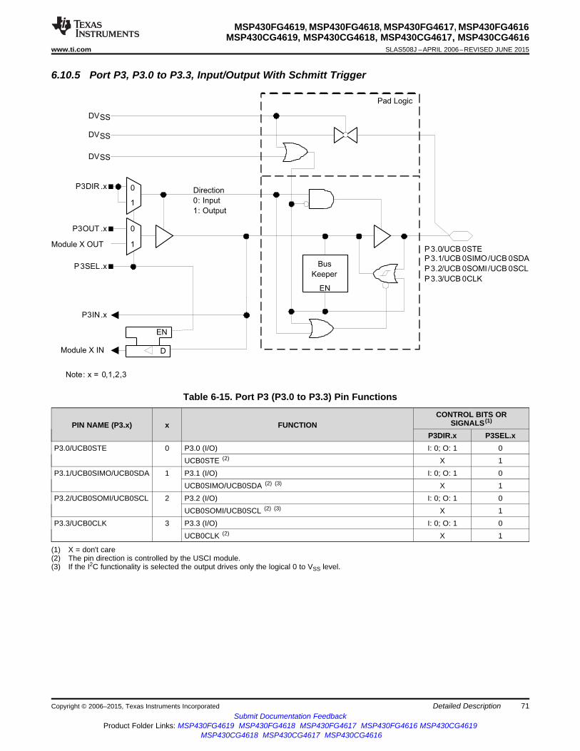
Bus
Keeper
EN
Direction
0: Input
1: Output
P3SEL.x
1
0P3DIR .x
P3IN.x
DVSS
DVSS
Pad Logic
DVSS
D
EN
Module X IN
1
0
Module X OUT
P3OUT .x
Note: x = 0,1,2,3
P3.0/UCB 0STE
P3.1/UCB 0SIMO/UCB 0SDA
P3.2/UCB 0SOMI /UCB 0SCL
P3.3/UCB 0CLK
MSP430FG4619, MSP430FG4618, MSP430FG4617, MSP430FG4616MSP430CG4619, MSP430CG4618, MSP430CG4617, MSP430CG4616
www.ti.com SLAS508J –APRIL 2006–REVISED JUNE 2015
6.10.5 Port P3, P3.0 to P3.3, Input/Output With Schmitt Trigger
Table 6-15. Port P3 (P3.0 to P3.3) Pin Functions
CONTROL BITS ORSIGNALS (1)PIN NAME (P3.x) x FUNCTION
P3DIR.x P3SEL.xP3.0/UCB0STE 0 P3.0 (I/O) I: 0; O: 1 0
UCB0STE (2) X 1P3.1/UCB0SIMO/UCB0SDA 1 P3.1 (I/O) I: 0; O: 1 0
UCB0SIMO/UCB0SDA (2) (3) X 1P3.2/UCB0SOMI/UCB0SCL 2 P3.2 (I/O) I: 0; O: 1 0
UCB0SOMI/UCB0SCL (2) (3) X 1P3.3/UCB0CLK 3 P3.3 (I/O) I: 0; O: 1 0
UCB0CLK (2) X 1
(1) X = don't care(2) The pin direction is controlled by the USCI module.(3) If the I2C functionality is selected the output drives only the logical 0 to VSS level.
Copyright © 2006–2015, Texas Instruments Incorporated Detailed Description 71Submit Documentation Feedback
Product Folder Links: MSP430FG4619 MSP430FG4618 MSP430FG4617 MSP430FG4616 MSP430CG4619MSP430CG4618 MSP430CG4617 MSP430CG4616

Bus
Keeper
EN
Direction
0: Input
1: Output
P3SEL.x
1
0P3DIR .x
P3IN.x
DVSS
DVSS
Pad Logic
TBOUTH
D
EN
Module X IN
1
0
Module X OUT
P3OUT .x
Note: x = 4,5,6,7
P3.4/TB3
P3.5/TB4
P3.6/TB5
P3.7/TB6
MSP430FG4619, MSP430FG4618, MSP430FG4617, MSP430FG4616MSP430CG4619, MSP430CG4618, MSP430CG4617, MSP430CG4616SLAS508J –APRIL 2006–REVISED JUNE 2015 www.ti.com
6.10.6 Port P3, P3.4 to P3.7, Input/Output With Schmitt Trigger
Table 6-16. Port P3 (P3.4 to P3.7) Pin Functions
CONTROL BITS OR SIGNALSPIN NAME (P3.x) x FUNCTION
P3DIR.x P3SEL.xP3.4/TB3 4 P3.4 (I/O) I: 0; O: 1 0
Timer_B7.CCI3A and Timer_B7.CCI3B 0 1Timer_B7.TB3 (1) 1 1
P3.5/TB4 5 P3.5 (I/O) I: 0; O: 1 0Timer_B7.CCI4A and Timer_B7.CCI4B 0 1Timer_B7.TB4 (1) 1 1
P3.6/TB5 6 P3.6 (I/O) I: 0; O: 1 0Timer_B7.CCI5A and Timer_B7.CCI5B 0 1Timer_B7.TB5 (1) 1 1
P3.7/TB6 7 P3.7 (I/O) I: 0; O: 1 0Timer_B7.CCI6A and Timer_B7.CCI6B 0 1Timer_B7.TB6 (1) 1 1
(1) Setting TBOUTH causes all Timer_B outputs to be set to high impedance.
72 Detailed Description Copyright © 2006–2015, Texas Instruments IncorporatedSubmit Documentation Feedback
Product Folder Links: MSP430FG4619 MSP430FG4618 MSP430FG4617 MSP430FG4616 MSP430CG4619MSP430CG4618 MSP430CG4617 MSP430CG4616

Bus
Keeper
EN
Direction
0: Input
1: Output
P4SEL.x
1
0P4DIR.x
P4IN.x
DVSS
DVSS
Pad Logic
DVSS
D
EN
Module X IN
1
0
Module X OUT
P4OUT.x
Note: x = 0,1
P4.1/URXD 1
P4.0/UTXD 1
Direction control
from Module X
MSP430FG4619, MSP430FG4618, MSP430FG4617, MSP430FG4616MSP430CG4619, MSP430CG4618, MSP430CG4617, MSP430CG4616
www.ti.com SLAS508J –APRIL 2006–REVISED JUNE 2015
6.10.7 Port P4, P4.0 to P4.1, Input/Output With Schmitt Trigger
Table 6-17. Port P4 (P4.0 to P4.1) Pin Functions
CONTROL BITS ORSIGNALS (1)PIN NAME (P4.x) x FUNCTION
P4DIR.x P4SEL.xP4.0/UTXD1 0 P4.0 (I/O) I: 0; O: 1 0
USART1.UTXD1 (2) X 1P4.1/URXD1 1 P4.1 (I/O) I: 0; O: 1 0
USART1.URXD1 (2) X 1
(1) X = don't care(2) When in USART1 mode, P4.0 is set to output, P4.1 is set to input.
Copyright © 2006–2015, Texas Instruments Incorporated Detailed Description 73Submit Documentation Feedback
Product Folder Links: MSP430FG4619 MSP430FG4618 MSP430FG4617 MSP430FG4616 MSP430CG4619MSP430CG4618 MSP430CG4617 MSP430CG4616

Bus
Keeper
EN
Direction
0: Input
1: Output
P4SEL.x
1
0P4DIR.x
P4IN.x
LCDS 32/36
Segment Sy
Pad Logic
DVSS
D
EN
Module X IN
1
0
Module X OUT
P4OUT.x
Note : x = 2,3,4,5,6,7
y = 34,35,36,37,38,39
P4.7/UCA0RXD /S34
P4.6/UCA0TXD/S35
P4.5/UCLK1/S36
P4.4/SOMI1/S37
P4.3/SIMO1/S38
P4.2/STE1/S39
Direction control
from Module X
MSP430FG4619, MSP430FG4618, MSP430FG4617, MSP430FG4616MSP430CG4619, MSP430CG4618, MSP430CG4617, MSP430CG4616SLAS508J –APRIL 2006–REVISED JUNE 2015 www.ti.com
6.10.8 Port P4, P4.2 to P4.7, Input/Output With Schmitt Trigger
Table 6-18. Port P4 (P4.2 to P4.5) Pin Functions
CONTROL BITS OR SIGNALS (1)PIN NAME (P4.x) x FUNCTION
P4DIR.x P4SEL.x LCDS36P4.2 (I/O) I: 0; O: 1 0 0
P4.2/STE1/S39 2 USART1.STE1 X 1 0S39 X X 1P4.3 (I/O) I: 0; O: 1 0 0
P4.3/SIMO/S38 3 USART1.SIMO1 (2) X 1 0S38 X X 1P4.4 (I/O) I: 0; O: 1 0 0
P4.4/SOMI/S37 4 USART1.SOMI1 (2) X 1 0S37 X X 1P4.5 (I/O) I: 0; O: 1 0 0
P4.5/SOMI/S36 5 USART1.UCLK1 (2) X 1 0S36 X X 1
(1) X = don't care(2) The pin direction is controlled by the USART1 module.
74 Detailed Description Copyright © 2006–2015, Texas Instruments IncorporatedSubmit Documentation Feedback
Product Folder Links: MSP430FG4619 MSP430FG4618 MSP430FG4617 MSP430FG4616 MSP430CG4619MSP430CG4618 MSP430CG4617 MSP430CG4616
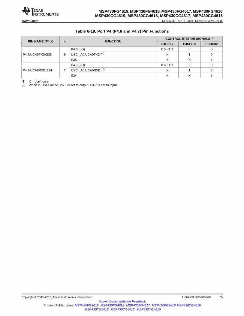
MSP430FG4619, MSP430FG4618, MSP430FG4617, MSP430FG4616MSP430CG4619, MSP430CG4618, MSP430CG4617, MSP430CG4616
www.ti.com SLAS508J –APRIL 2006–REVISED JUNE 2015
Table 6-19. Port P4 (P4.6 and P4.7) Pin Functions
CONTROL BITS OR SIGNALS (1)PIN NAME (P4.x) x FUNCTION
P4DIR.x P4SEL.x LCDS32P4.6 (I/O) I: 0; O: 1 0 0
P4.6/UCA0TXD/S35 6 USCI_A0.UCA0TXD (2) X 1 0S35 X X 1P4.7 (I/O) I: 0; O: 1 0 0
P4.7/UCA0RXD/S34 7 USCI_A0.UCA0RXD (2) X 1 0S34 X X 1
(1) X = don't care(2) When in USCI mode, P4.6 is set to output, P4.7 is set to input.
Copyright © 2006–2015, Texas Instruments Incorporated Detailed Description 75Submit Documentation Feedback
Product Folder Links: MSP430FG4619 MSP430FG4618 MSP430FG4617 MSP430FG4616 MSP430CG4619MSP430CG4618 MSP430CG4617 MSP430CG4616

Bus
Keeper
EN
Direction
0: Input
1: Output
P5SEL.x
1
0P5DIR.x
P5IN.x
LCDS 0
Segment Sy
1
0P5OUT.x
P5.0/S1/A13/OA 1I1
DVSS
INCH=13#
A13#
Pad Logic
-
+OA1
Note: x = 0
y = 1
MSP430FG4619, MSP430FG4618, MSP430FG4617, MSP430FG4616MSP430CG4619, MSP430CG4618, MSP430CG4617, MSP430CG4616SLAS508J –APRIL 2006–REVISED JUNE 2015 www.ti.com
6.10.9 Port P5, P5.0, Input/Output With Schmitt Trigger
Table 6-20. Port P5 (P5.0) Pin Functions
CONTROL BITS OR SIGNALS (1)
PIN NAME (P5.x) x FUNCTION OAPx (OA1)P5DIR.x P5SEL.x INCHx LCDS0OANx (OA1)P5.0/S1/A13/OA1I1 0 P5.0 (I/O) I: 0; O: 1 0 X X 0
OAI11 0 X X 1 0A13 (2) X 1 13 X XS1 enabled X 0 X X 1S1 disabled X 1 X X 1
(1) X = don't care(2) Setting the P5SEL.x bit disables the output driver and the input Schmitt trigger to prevent parasitic cross currents when applying analog
signals.
76 Detailed Description Copyright © 2006–2015, Texas Instruments IncorporatedSubmit Documentation Feedback
Product Folder Links: MSP430FG4619 MSP430FG4618 MSP430FG4617 MSP430FG4616 MSP430CG4619MSP430CG4618 MSP430CG4617 MSP430CG4616
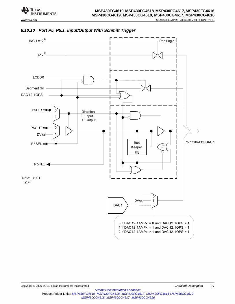
Bus
Keeper
EN
Direction
0: Input
1: Output
P5SEL.x
1
0P5DIR.x
P5IN.x
LCDS0
Segment Sy
1
0P5OUT.x
P5.1/S0/A12/DAC 1
DVSS
INCH =12#
A12#
Pad Logic
DAC 12.1OPS
DAC1
1
0
2
DVSS
0 if DAC12.1AMPx = 0 and DAC 12.1OPS = 1
1 if DAC12.1AMPx = 1 and DAC 12.1OPS = 1
2 if DAC12.1AMPx > 1 and DAC 12.1OPS = 1
Note: x = 1
y = 0
MSP430FG4619, MSP430FG4618, MSP430FG4617, MSP430FG4616MSP430CG4619, MSP430CG4618, MSP430CG4617, MSP430CG4616
www.ti.com SLAS508J –APRIL 2006–REVISED JUNE 2015
6.10.10 Port P5, P5.1, Input/Output With Schmitt Trigger
Copyright © 2006–2015, Texas Instruments Incorporated Detailed Description 77Submit Documentation Feedback
Product Folder Links: MSP430FG4619 MSP430FG4618 MSP430FG4617 MSP430FG4616 MSP430CG4619MSP430CG4618 MSP430CG4617 MSP430CG4616

MSP430FG4619, MSP430FG4618, MSP430FG4617, MSP430FG4616MSP430CG4619, MSP430CG4618, MSP430CG4617, MSP430CG4616SLAS508J –APRIL 2006–REVISED JUNE 2015 www.ti.com
Table 6-21. Port P5 (P5.1) Pin FunctionsCONTROL BITS OR SIGNALS (1)
PIN NAME (P5.x) x FUNCTIONP5DIR.x P5SEL.x INCHx DAC12.1OPS DAC12.1AMPx LCDS0
P5.1/S0/A12/DAC1 1 P5.1 (I/O) I: 0; O: 1 0 X 0 X 0
DAC1 high impedance X X X 1 0 X
DVSS X X X 1 1 X
DAC1 output X X X 1 >1 X
A12 (2) X 1 12 0 X 0
S0 enabled X 0 X 0 X 1
S0 disabled X 1 X 0 X 1
(1) X = don't care(2) Setting the P5SEL.x bit disables the output driver and the input Schmitt trigger to prevent parasitic cross currents when applying analog
signals.
78 Detailed Description Copyright © 2006–2015, Texas Instruments IncorporatedSubmit Documentation Feedback
Product Folder Links: MSP430FG4619 MSP430FG4618 MSP430FG4617 MSP430FG4616 MSP430CG4619MSP430CG4618 MSP430CG4617 MSP430CG4616

Bus
Keeper
EN
Direction
0: Input
1: Output
P5SEL.x
1
0P5DIR.x
P5IN.x
LCD Signal
Pad Logic
DVSS
1
0P5OUT.x
Note : x = 2,3,4
P5.2/COM1
P5.3/COM2
P5.4/COM3
DVSS
MSP430FG4619, MSP430FG4618, MSP430FG4617, MSP430FG4616MSP430CG4619, MSP430CG4618, MSP430CG4617, MSP430CG4616
www.ti.com SLAS508J –APRIL 2006–REVISED JUNE 2015
6.10.11 Port P5, P5.2 to P5.4, Input/Output With Schmitt Trigger
Table 6-22. Port P5 (P5.2 to P5.4) Pin Functions
CONTROL BITS ORSIGNALS (1)PIN NAME (P5.x) x FUNCTION
P5DIR.x P5SEL.xP5.2/COM1 2 P5.2 (I/O) I: 0; O: 1 0
COM1 X 1P5.3/COM2 3 P5.3 (I/O) I: 0; O: 1 0
COM2 X 1P5.4/COM3 4 P5.4 (I/O) I: 0; O: 1 0
COM3 X 1
(1) X = don't care
Copyright © 2006–2015, Texas Instruments Incorporated Detailed Description 79Submit Documentation Feedback
Product Folder Links: MSP430FG4619 MSP430FG4618 MSP430FG4617 MSP430FG4616 MSP430CG4619MSP430CG4618 MSP430CG4617 MSP430CG4616
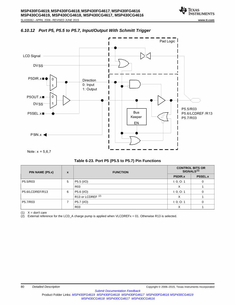
Bus
Keeper
EN
Direction
0: Input
1: Output
P5SEL.x
1
0P5DIR.x
P5IN.x
LCD Signal
Pad Logic
DVSS
1
0P5OUT.x
Note : x = 5,6,7
P5.5/R03
P5.6/LCDREF /R13
P5.7/R03
DVSS
MSP430FG4619, MSP430FG4618, MSP430FG4617, MSP430FG4616MSP430CG4619, MSP430CG4618, MSP430CG4617, MSP430CG4616SLAS508J –APRIL 2006–REVISED JUNE 2015 www.ti.com
6.10.12 Port P5, P5.5 to P5.7, Input/Output With Schmitt Trigger
Table 6-23. Port P5 (P5.5 to P5.7) Pin Functions
CONTROL BITS ORSIGNALS (1)PIN NAME (P5.x) x FUNCTION
P5DIR.x P5SEL.xP5.5/R03 5 P5.5 (I/O) I: 0; O: 1 0
R03 X 1P5.6/LCDREF/R13 6 P5.6 (I/O) I: 0; O: 1 0
R13 or LCDREF (2) X 1P5.7/R03 7 P5.7 (I/O) I: 0; O: 1 0
R03 X 1
(1) X = don't care(2) External reference for the LCD_A charge pump is applied when VLCDREFx = 01. Otherwise R13 is selected.
80 Detailed Description Copyright © 2006–2015, Texas Instruments IncorporatedSubmit Documentation Feedback
Product Folder Links: MSP430FG4619 MSP430FG4618 MSP430FG4617 MSP430FG4616 MSP430CG4619MSP430CG4618 MSP430CG4617 MSP430CG4616

Bus
Keeper
EN
Direction
0: Input
1: Output
P6SEL.x
1
0P6DIR.x
P6IN.x
INCH =0/2/4#
Ay#
Pad Logic
1
0
DVSS
P6OUT.x
P6.0/A0/OA 0I0
P6.2/A2/OA 0I1
P6.4/A4/OA 1I0
-
+OA0/1
Note: x = 0, 2, 4
y = 0, 1
# = Signal from or to ADC12
MSP430FG4619, MSP430FG4618, MSP430FG4617, MSP430FG4616MSP430CG4619, MSP430CG4618, MSP430CG4617, MSP430CG4616
www.ti.com SLAS508J –APRIL 2006–REVISED JUNE 2015
6.10.13 Port P6, P6.0, P6.2, and P6.4, Input/Output With Schmitt Trigger
Table 6-24. Port P6 (P6.0, P6.2, and P6.4) Pin Functions
CONTROL BITS OR SIGNALS (1)
PIN NAME (P6.x) x FUNCTION OAPx (OA0) OAPx (OA1)P6DIR.x P6SEL.x INCHxOANx (OA0) OANx (OA1)P6.0/A0/OA0I0 0 P6.0 (I/O) I: 0; O: 1 0 X X X
OA0I0 0 X 0 X XA0 (2) X 1 X X 0
P6.2/A2/OA0I1 2 P6.2 (I/O) I: 0; O: 1 0 X X XOA0I1 0 X 1 X XA2 (2) X 1 X X 2
P6.4/A4/OA1I0 4 P6.4 (I/O) I: 0; O: 1 0 X X XOA1I0 0 X X 0 XA4 (2) X 1 X X 4
(1) X = don't care(2) Setting the P6SEL.x bit disables the output driver and the input Schmitt trigger to prevent parasitic cross currents when applying analog
signals.
Copyright © 2006–2015, Texas Instruments Incorporated Detailed Description 81Submit Documentation Feedback
Product Folder Links: MSP430FG4619 MSP430FG4618 MSP430FG4617 MSP430FG4616 MSP430CG4619MSP430CG4618 MSP430CG4617 MSP430CG4616
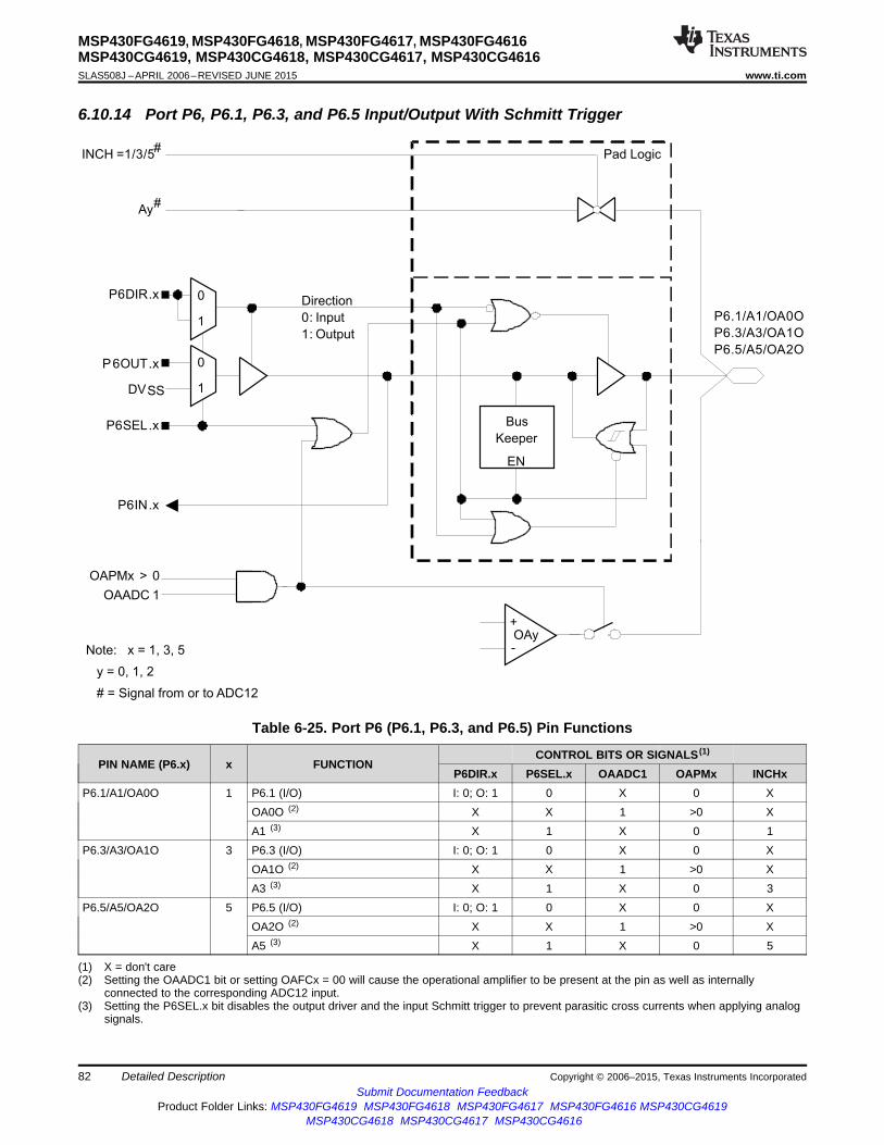
Bus
Keeper
EN
Direction
0: Input
1: Output
P6SEL.x
1
0P6DIR.x
P6IN.x
INCH =1/3/5#
Ay#
Pad Logic
1
0
DVSS
P6OUT.x
P6.1/A1/OA0O
P6.3/A3/OA1O
P6.5/A5/OA2O
-
+OAy
OAPMx > 0
OAADC 1
Note: x = 1, 3, 5
y = 0, 1, 2
# = Signal from or to ADC12
MSP430FG4619, MSP430FG4618, MSP430FG4617, MSP430FG4616MSP430CG4619, MSP430CG4618, MSP430CG4617, MSP430CG4616SLAS508J –APRIL 2006–REVISED JUNE 2015 www.ti.com
6.10.14 Port P6, P6.1, P6.3, and P6.5 Input/Output With Schmitt Trigger
Table 6-25. Port P6 (P6.1, P6.3, and P6.5) Pin Functions
CONTROL BITS OR SIGNALS (1)PIN NAME (P6.x) x FUNCTION
P6DIR.x P6SEL.x OAADC1 OAPMx INCHxP6.1/A1/OA0O 1 P6.1 (I/O) I: 0; O: 1 0 X 0 X
OA0O (2) X X 1 >0 XA1 (3) X 1 X 0 1
P6.3/A3/OA1O 3 P6.3 (I/O) I: 0; O: 1 0 X 0 XOA1O (2) X X 1 >0 XA3 (3) X 1 X 0 3
P6.5/A5/OA2O 5 P6.5 (I/O) I: 0; O: 1 0 X 0 XOA2O (2) X X 1 >0 XA5 (3) X 1 X 0 5
(1) X = don't care(2) Setting the OAADC1 bit or setting OAFCx = 00 will cause the operational amplifier to be present at the pin as well as internally
connected to the corresponding ADC12 input.(3) Setting the P6SEL.x bit disables the output driver and the input Schmitt trigger to prevent parasitic cross currents when applying analog
signals.
82 Detailed Description Copyright © 2006–2015, Texas Instruments IncorporatedSubmit Documentation Feedback
Product Folder Links: MSP430FG4619 MSP430FG4618 MSP430FG4617 MSP430FG4616 MSP430CG4619MSP430CG4618 MSP430CG4617 MSP430CG4616
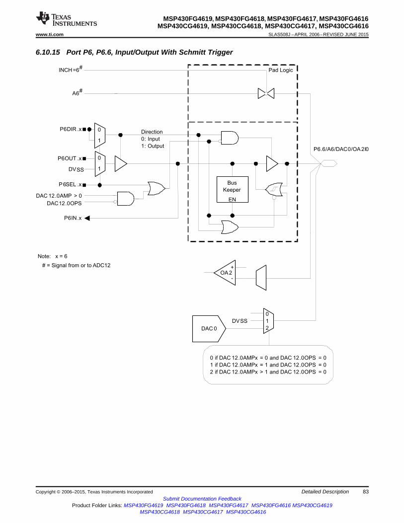
Bus
Keeper
EN
Direction
0: Input
1: Output
P6SEL .x
1
0P6DIR .x
P6IN.x
INCH=6#
A6#
Pad Logic
1
0
DVSS
P6OUT .x
P6.6/A6/DAC0/OA 2I0
-
+OA 2
DAC 0
DAC12.0OPS
DAC 12.0AMP > 0
1
0
2
0 if DAC 12.0AMPx = 0 and DAC 12.0OPS = 0
1 if DAC 12.0AMPx = 1 and DAC 12.0OPS = 0
2 if DAC 12.0AMPx > 1 and DAC 12.0OPS = 0
DVSS
Note: x = 6
# = Signal from or to ADC12
MSP430FG4619, MSP430FG4618, MSP430FG4617, MSP430FG4616MSP430CG4619, MSP430CG4618, MSP430CG4617, MSP430CG4616
www.ti.com SLAS508J –APRIL 2006–REVISED JUNE 2015
6.10.15 Port P6, P6.6, Input/Output With Schmitt Trigger
Copyright © 2006–2015, Texas Instruments Incorporated Detailed Description 83Submit Documentation Feedback
Product Folder Links: MSP430FG4619 MSP430FG4618 MSP430FG4617 MSP430FG4616 MSP430CG4619MSP430CG4618 MSP430CG4617 MSP430CG4616

MSP430FG4619, MSP430FG4618, MSP430FG4617, MSP430FG4616MSP430CG4619, MSP430CG4618, MSP430CG4617, MSP430CG4616SLAS508J –APRIL 2006–REVISED JUNE 2015 www.ti.com
Table 6-26. Port P6 (P6.6) Pin FunctionsCONTROL BITS OR SIGNALS (1)
PIN NAME (P6.x) x FUNCTION OAPx (OA2)P6DIR.x P6SEL.x INCHx DAC12.0OPS DAC12.0AMPx OANx (OA2)
P6.6/A6/DAC0/OA2I0 6 P6.6 (I/O) I: 0; O: 1 0 X 1 X X
DAC0 high impedance X X X 0 0 X
DVSS X X X 0 1 X
DAC0 output X X X 0 >1 X
A6 (2) X 1 6 X X X
OA2I0 0 X 0 X X 0
(1) X = don't care(2) Setting the P6SEL.x bit disables the output driver and the input Schmitt trigger to prevent parasitic cross currents when applying analog
signals.
84 Detailed Description Copyright © 2006–2015, Texas Instruments IncorporatedSubmit Documentation Feedback
Product Folder Links: MSP430FG4619 MSP430FG4618 MSP430FG4617 MSP430FG4616 MSP430CG4619MSP430CG4618 MSP430CG4617 MSP430CG4616

Bus
Keeper
EN
Direction
0: Input
1: Output
P6SEL .x
1
0P6DIR .x
P6IN.x
INCH=7#
A7#
Pad Logic
1
0
DVSS
P6OUT .x
P6.7/A7/DAC 1/SVSIN
DAC 1
DAC12.1OPS
DAC 12.1AMP > 0
1
0
2
0 if DAC 12.1AMPx = 0 and DAC 12.1OPS = 0
1 if DAC 12.1AMPx = 1 and DAC 12.1OPS = 0
2 if DAC 12.1AMPx > 1 and DAC 12.1OPS = 0
To SVS Mux
VLD =15
DVSS
Note: x = 7
# = Signal from or to ADC12
MSP430FG4619, MSP430FG4618, MSP430FG4617, MSP430FG4616MSP430CG4619, MSP430CG4618, MSP430CG4617, MSP430CG4616
www.ti.com SLAS508J –APRIL 2006–REVISED JUNE 2015
6.10.16 Port P6, P6.7, Input/Output With Schmitt Trigger
Copyright © 2006–2015, Texas Instruments Incorporated Detailed Description 85Submit Documentation Feedback
Product Folder Links: MSP430FG4619 MSP430FG4618 MSP430FG4617 MSP430FG4616 MSP430CG4619MSP430CG4618 MSP430CG4617 MSP430CG4616

MSP430FG4619, MSP430FG4618, MSP430FG4617, MSP430FG4616MSP430CG4619, MSP430CG4618, MSP430CG4617, MSP430CG4616SLAS508J –APRIL 2006–REVISED JUNE 2015 www.ti.com
Table 6-27. Port P6 (P6.7) Pin FunctionsCONTROL BITS OR SIGNALS (1)
PIN NAME (P6.x) x FUNCTIONP6DIR.x P6SEL.x INCHx DAC12.1OPS DAC12.1AMPx
P6.7/A7/DAC1/SVSIN 7 P6.7 (I/O) I: 0; O: 1 0 X 1 X
DAC1 high impedance X X X 0 0
DVSS X X X 0 1
DAC1 output X X X 0 >1
A7 (2) X 1 7 X X
SVSIN (2) 0 1 0 1 X
(1) X = don't care(2) Setting the P6SEL.x bit disables the output driver and the input Schmitt trigger to prevent parasitic cross currents when applying analog
signals.
86 Detailed Description Copyright © 2006–2015, Texas Instruments IncorporatedSubmit Documentation Feedback
Product Folder Links: MSP430FG4619 MSP430FG4618 MSP430FG4617 MSP430FG4616 MSP430CG4619MSP430CG4618 MSP430CG4617 MSP430CG4616
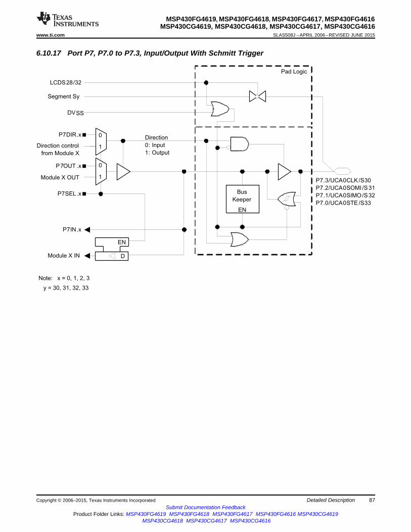
Bus
Keeper
EN
Direction
0: Input
1: Output
P7SEL.x
1
0P7DIR.x
P7IN.x
LCDS28/32
Segment Sy
Pad Logic
DVSS
D
EN
Module X IN
1
0
Module X OUT
P7OUT .x
P7.3/UCA0CLK /S30
P7.2/UCA0SOMI /S31
P7.1/UCA0SIMO/S32
P7.0/UCA0STE /S33
Direction control
from Module X
Note: x = 0, 1, 2, 3
y = 30, 31, 32, 33
MSP430FG4619, MSP430FG4618, MSP430FG4617, MSP430FG4616MSP430CG4619, MSP430CG4618, MSP430CG4617, MSP430CG4616
www.ti.com SLAS508J –APRIL 2006–REVISED JUNE 2015
6.10.17 Port P7, P7.0 to P7.3, Input/Output With Schmitt Trigger
Copyright © 2006–2015, Texas Instruments Incorporated Detailed Description 87Submit Documentation Feedback
Product Folder Links: MSP430FG4619 MSP430FG4618 MSP430FG4617 MSP430FG4616 MSP430CG4619MSP430CG4618 MSP430CG4617 MSP430CG4616
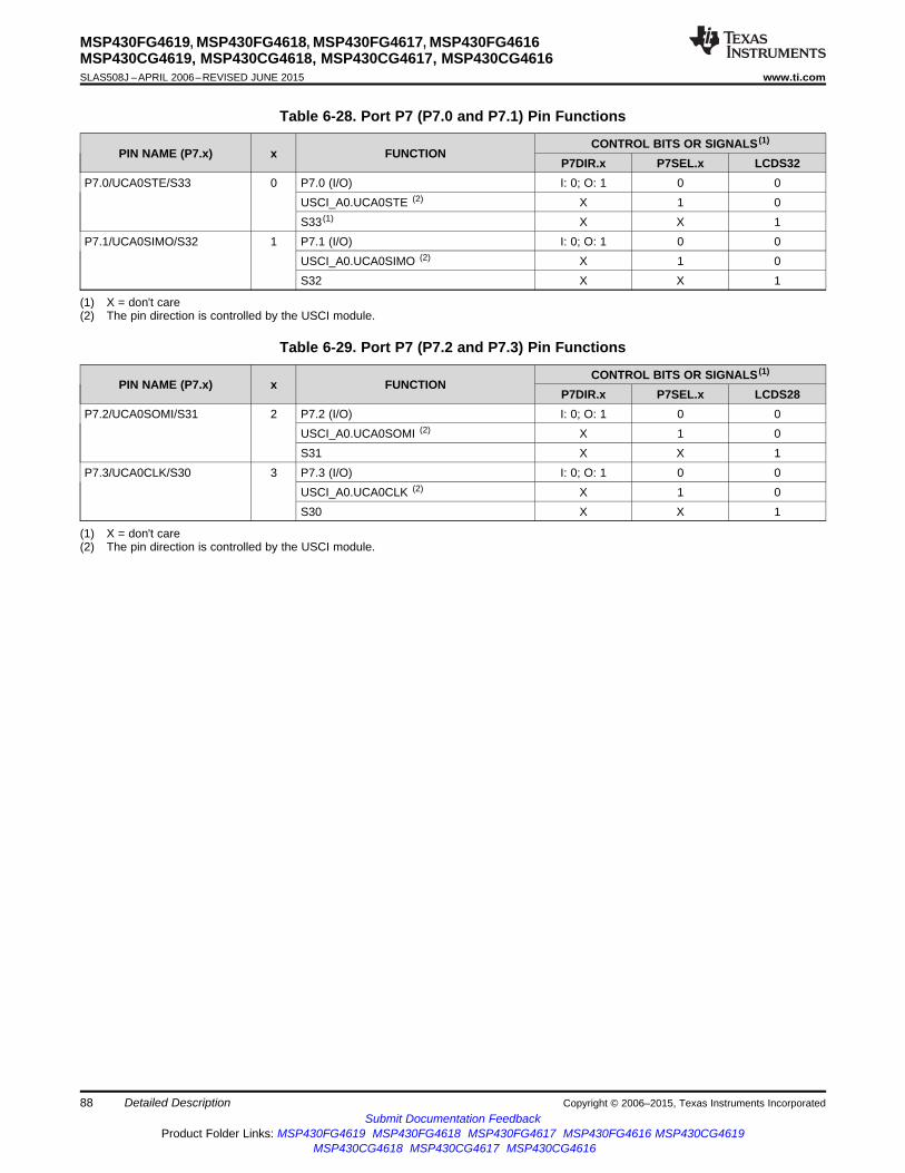
MSP430FG4619, MSP430FG4618, MSP430FG4617, MSP430FG4616MSP430CG4619, MSP430CG4618, MSP430CG4617, MSP430CG4616SLAS508J –APRIL 2006–REVISED JUNE 2015 www.ti.com
Table 6-28. Port P7 (P7.0 and P7.1) Pin Functions
CONTROL BITS OR SIGNALS (1)PIN NAME (P7.x) x FUNCTION
P7DIR.x P7SEL.x LCDS32P7.0/UCA0STE/S33 0 P7.0 (I/O) I: 0; O: 1 0 0
USCI_A0.UCA0STE (2) X 1 0S33 (1) X X 1
P7.1/UCA0SIMO/S32 1 P7.1 (I/O) I: 0; O: 1 0 0USCI_A0.UCA0SIMO (2) X 1 0S32 X X 1
(1) X = don't care(2) The pin direction is controlled by the USCI module.
Table 6-29. Port P7 (P7.2 and P7.3) Pin Functions
CONTROL BITS OR SIGNALS (1)PIN NAME (P7.x) x FUNCTION
P7DIR.x P7SEL.x LCDS28P7.2/UCA0SOMI/S31 2 P7.2 (I/O) I: 0; O: 1 0 0
USCI_A0.UCA0SOMI (2) X 1 0S31 X X 1
P7.3/UCA0CLK/S30 3 P7.3 (I/O) I: 0; O: 1 0 0USCI_A0.UCA0CLK (2) X 1 0S30 X X 1
(1) X = don't care(2) The pin direction is controlled by the USCI module.
88 Detailed Description Copyright © 2006–2015, Texas Instruments IncorporatedSubmit Documentation Feedback
Product Folder Links: MSP430FG4619 MSP430FG4618 MSP430FG4617 MSP430FG4616 MSP430CG4619MSP430CG4618 MSP430CG4617 MSP430CG4616

Bus
Keeper
EN
Direction
0: Input
1: Output
P7SEL.x
1
0P7DIR.x
P7IN.x
LCDS 24/28
Segment Sy
Pad Logic
DVSS
1
0P7OUT.x
P7.7/S26
P7.6/S27
P7.5/S28
P7.4/S29
DVSS
Note: x = 4, 5, 6, 7
y = 26, 27, 28, 29
MSP430FG4619, MSP430FG4618, MSP430FG4617, MSP430FG4616MSP430CG4619, MSP430CG4618, MSP430CG4617, MSP430CG4616
www.ti.com SLAS508J –APRIL 2006–REVISED JUNE 2015
6.10.18 Port P7, P7.4 to P7.7, Input/Output With Schmitt Trigger
Table 6-30. Port P7 (P7.4 and P7.5) Pin Functions
CONTROL BITS OR SIGNALS (1)PIN NAME (P7.x) x FUNCTION
P7DIR.x P7SEL.x LCDS28P7.4/S29 4 P7.4 (I/O) I: 0; O: 1 0 0
S29 X X 1P7.5/S28 5 P7.5 (I/O) I: 0; O: 1 0 0
S28 X X 1
(1) X = don't care
Table 6-31. Port P7 (P7.6 and P7.7) Pin Functions
CONTROL BITS OR SIGNALS (1)PIN NAME (P7.x) x FUNCTION
P7DIR.x P7SEL.x LCDS24P7.6/S27 6 P7.6 (I/O) I: 0; O: 1 0 0
S27 X X 1P7.7/S26 7 P7.7 (I/O) I: 0; O: 1 0 0
S26 X X 1
(1) X = don't care
Copyright © 2006–2015, Texas Instruments Incorporated Detailed Description 89Submit Documentation Feedback
Product Folder Links: MSP430FG4619 MSP430FG4618 MSP430FG4617 MSP430FG4616 MSP430CG4619MSP430CG4618 MSP430CG4617 MSP430CG4616

Bus
Keeper
EN
Direction
0: Input
1: Output
P8SEL.x
1
0P8DIR.x
P8IN.x
LCDS 16/20/24
Segment Sy
Pad Logic
DVSS
1
0P8OUT.x
Note : x = 0,1,2,3,4,5,6,7
y = 25,24,23,22,21,20,19,18
P8.7/S18
P8.6/S19
P8.5/S20
P8.4/S21
P8.3/S22
P8.2/S23
P8.1/S24
P8.0/S25
DVSS
MSP430FG4619, MSP430FG4618, MSP430FG4617, MSP430FG4616MSP430CG4619, MSP430CG4618, MSP430CG4617, MSP430CG4616SLAS508J –APRIL 2006–REVISED JUNE 2015 www.ti.com
6.10.19 Port P8, P8.0 to P8.7, Input/Output With Schmitt Trigger
Table 6-32. Port P8 (P8.0 and P8.1) Pin Functions
CONTROL BITS OR SIGNALS (1)PIN NAME (P8.x) x FUNCTION
P8DIR.x P8SEL.x LCDS16P8.0/S18 0 P8.0 (I/O) I: 0; O: 1 0 0
S18 X X 1P8.1/S19 0 P8.0 (I/O) I: 0; O: 1 0 0
S19 X X 1
(1) X = don't care
Table 6-33. Port P8 (P8.2 to P8.5) Pin Functions
CONTROL BITS OR SIGNALS (1)PIN NAME (P8.x) x FUNCTION
P8DIR.x P8SEL.x LCDS20P8.2/S20 2 P8.2 (I/O) I: 0; O: 1 0 0
S20 X X 1P8.3/S21 3 P8.3 (I/O) I: 0; O: 1 0 0
S21 X X 1P8.4/S22 4 P8.4 (I/O) I: 0; O: 1 0 0
S22 X X 1P8.5/S23 5 P8.5 (I/O) I: 0; O: 1 0 0
S23 X X 1
(1) X = don't care
90 Detailed Description Copyright © 2006–2015, Texas Instruments IncorporatedSubmit Documentation Feedback
Product Folder Links: MSP430FG4619 MSP430FG4618 MSP430FG4617 MSP430FG4616 MSP430CG4619MSP430CG4618 MSP430CG4617 MSP430CG4616
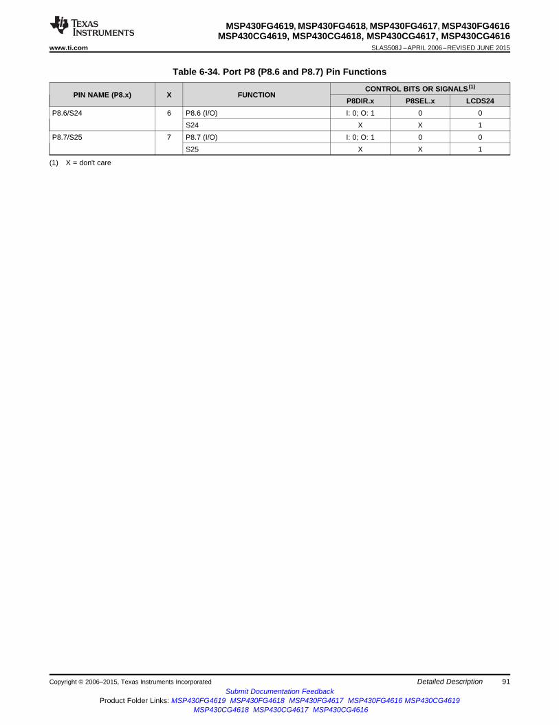
MSP430FG4619, MSP430FG4618, MSP430FG4617, MSP430FG4616MSP430CG4619, MSP430CG4618, MSP430CG4617, MSP430CG4616
www.ti.com SLAS508J –APRIL 2006–REVISED JUNE 2015
Table 6-34. Port P8 (P8.6 and P8.7) Pin Functions
CONTROL BITS OR SIGNALS (1)PIN NAME (P8.x) X FUNCTION
P8DIR.x P8SEL.x LCDS24P8.6/S24 6 P8.6 (I/O) I: 0; O: 1 0 0
S24 X X 1P8.7/S25 7 P8.7 (I/O) I: 0; O: 1 0 0
S25 X X 1
(1) X = don't care
Copyright © 2006–2015, Texas Instruments Incorporated Detailed Description 91Submit Documentation Feedback
Product Folder Links: MSP430FG4619 MSP430FG4618 MSP430FG4617 MSP430FG4616 MSP430CG4619MSP430CG4618 MSP430CG4617 MSP430CG4616

Bus
Keeper
EN
Direction
0: Input
1: Output
P9SEL.x
1
0P9DIR.x
P9IN.x
LCDS 8/12/16
Segment Sy
Pad Logic
DVSS
1
0P9OUT.x
Note : x = 0,1,2,3,4,5,6,7
y = 17,16,15,14,13,12,11 ,10
P9.7/S10
P9.6/S11
P9.5/S12
P9.4/S13
P9.3/S14
P9.2/S15
P9.1/S16
P9.0/S17
DVSS
MSP430FG4619, MSP430FG4618, MSP430FG4617, MSP430FG4616MSP430CG4619, MSP430CG4618, MSP430CG4617, MSP430CG4616SLAS508J –APRIL 2006–REVISED JUNE 2015 www.ti.com
6.10.20 Port P9, P9.0 to P9.7, Input/Output With Schmitt Trigger
Table 6-35. Port P9 (P9.0 and P9.1) Pin Functions
CONTROL BITS OR SIGNALS (1)PIN NAME (P9.x) x FUNCTION
P9DIR.x P9SEL.x LCDS16P9.0/S17 0 P9.0 (I/O) I: 0; O: 1 0 0
S17 X X 1P9.1/S16 1 P9.1 (I/O) I: 0; O: 1 0 0
S16 X X 1
(1) X = don't care
Table 6-36. Port P9 (P9.2 to P9.5) Pin Functions
CONTROL BITS OR SIGNALS (1)PIN NAME (P9.x) x FUNCTION
P9DIR.x P9SEL.x LCDS12P9.2/S15 2 P9.2 (I/O) I: 0; O: 1 0 0
S15 X X 1P9.3/S14 3 P9.3 (I/O) I: 0; O: 1 0 0
S14 X X 1P9.4/S13 4 P9.4 (I/O) I: 0; O: 1 0 0
S13 X X 1P9.5/S12 5 P9.5 (I/O) I: 0; O: 1 0 0
S12 X X 1
(1) X = don't care
92 Detailed Description Copyright © 2006–2015, Texas Instruments IncorporatedSubmit Documentation Feedback
Product Folder Links: MSP430FG4619 MSP430FG4618 MSP430FG4617 MSP430FG4616 MSP430CG4619MSP430CG4618 MSP430CG4617 MSP430CG4616

MSP430FG4619, MSP430FG4618, MSP430FG4617, MSP430FG4616MSP430CG4619, MSP430CG4618, MSP430CG4617, MSP430CG4616
www.ti.com SLAS508J –APRIL 2006–REVISED JUNE 2015
Table 6-37. Port P9 (P9.6 and P9.7) Pin Functions
CONTROL BITS OR SIGNALS (1)PIN NAME (P9.x x FUNCTION
P9DIR.x P9SEL.x LCDS8P9.6/S11 6 P9.6 (I/O) I: 0; O: 1 0 0
S11 X X 1P9.7/S10 7 P9.7 (I/O) I: 0; O: 1 0 0
S10 X X 1
(1) X = don't care
Copyright © 2006–2015, Texas Instruments Incorporated Detailed Description 93Submit Documentation Feedback
Product Folder Links: MSP430FG4619 MSP430FG4618 MSP430FG4617 MSP430FG4616 MSP430CG4619MSP430CG4618 MSP430CG4617 MSP430CG4616

Bus
Keeper
EN
Direction
0: Input
1: Output
P10SEL.x
1
0P10DIR.x
P10IN.x
LCDS 4/8
Segment Sy
Pad Logic
DVSS
1
0P10OUT.x
Note : x = 0,1,2,3,4,5
y = 9,8,7,6,5,4
P10.5/S4
P10.4/S5
P10.3/S6
P10.2/S7
P10.1/S8
P10.0/S9
DVSS
MSP430FG4619, MSP430FG4618, MSP430FG4617, MSP430FG4616MSP430CG4619, MSP430CG4618, MSP430CG4617, MSP430CG4616SLAS508J –APRIL 2006–REVISED JUNE 2015 www.ti.com
6.10.21 Port P10, P10.0 to P10.5, Input/Output With Schmitt Trigger
Table 6-38. Port P10 (P10.0 and P10.1) Pin Functions
CONTROL BITS OR SIGNALS (1)PIN NAME (P10.x) x FUNCTION
P10DIR.x P10SEL.x LCDS8P10.0/S9 0 P10.0 (I/O) I: 0; O: 1 0 0
S9 X X 1P10.1/S8 1 P10.1 (I/O) I: 0; O: 1 0 0
S8 X X 1
(1) X = don't care
Table 6-39. Port P10 (P10.2 to P10.5) Pin Functions
CONTROL BITS OR SIGNALS (1)PIN NAME (P10.x) x FUNCTION
P10DIR.x P10SEL.x LCDS4P10.2/S7 2 P10.2 (I/O) I: 0; O: 1 0 0
S7 X X 1P10.3/S6 3 P10.3 (I/O) I: 0; O: 1 0 0
S6 X X 1P10.4/S5 4 P10.4 (I/O) I: 0; O: 1 0 0
S5 X X 1P10.5/S4 5 P10.5 (I/O) I: 0; O: 1 0 0
S4 X X 1
(1) X = don't care
94 Detailed Description Copyright © 2006–2015, Texas Instruments IncorporatedSubmit Documentation Feedback
Product Folder Links: MSP430FG4619 MSP430FG4618 MSP430FG4617 MSP430FG4616 MSP430CG4619MSP430CG4618 MSP430CG4617 MSP430CG4616

Bus
Keeper
EN
Direction
0: Input
1: Output
P10SEL.x
1
0P10DIR.x
P10IN.x
LCDS 0
Segment Sy
1
0P10OUT.x
Note : x = 6
y = 3
P10.6/S3/A15
DVSS
INCH=15#
A15#
Pad Logic
MSP430FG4619, MSP430FG4618, MSP430FG4617, MSP430FG4616MSP430CG4619, MSP430CG4618, MSP430CG4617, MSP430CG4616
www.ti.com SLAS508J –APRIL 2006–REVISED JUNE 2015
6.10.22 Port P10, P10.6, Input/Output With Schmitt Trigger
Table 6-40. Port P10 (P10.6) Pin Functions
CONTROL BITS OR SIGNALS (1)PIN NAME (P10.x) x FUNCTION
P10DIR.x P10SEL.x INCHx LCDS0P10.6/S3/A15 P5.0 (I/O) I: 0; O: 1 0 X 0
A15 (2) X 1 15 06
S3 enabled X 0 X 1S3 disabled X 1 X 1
(1) X = don't care(2) Setting the P10SEL.x bit disables the output driver and the input Schmitt trigger to prevent parasitic cross currents when applying
analog signals.
Copyright © 2006–2015, Texas Instruments Incorporated Detailed Description 95Submit Documentation Feedback
Product Folder Links: MSP430FG4619 MSP430FG4618 MSP430FG4617 MSP430FG4616 MSP430CG4619MSP430CG4618 MSP430CG4617 MSP430CG4616

Bus
Keeper
EN
Direction
0: Input
1: Output
P10SEL.x
1
0P10DIR.x
P10IN.x
LCDS 0
Segment Sy
1
0P10OUT.x
Note : x = 7
y = 2
P10.7/S2/A14/OA 2I1
DVSS
INCH=14#
A14#
Pad Logic
-
+OA2
MSP430FG4619, MSP430FG4618, MSP430FG4617, MSP430FG4616MSP430CG4619, MSP430CG4618, MSP430CG4617, MSP430CG4616SLAS508J –APRIL 2006–REVISED JUNE 2015 www.ti.com
6.10.23 Port P10, P10.7, Input/Output With Schmitt Trigger
Table 6-41. Port P10 (P10.7) Pin Functions
CONTROL BITS OR SIGNALS (1)
PIN NAME (P10.x) x FUNCTION OAPx (OA1)P10DIR.x P10SEL.x INCHx LCDS0OANx (OA1)P10.7/S2/A14/OA2I1 7 P10.7(I/O) I: 0; O: 1 0 X X 0
A14 (2) X 1 14 X 0OA2I1 (2) 0 X X 1 0S2 enabled X 0 X X 1S2 disabled X 1 X X 1
(1) X = don't care(2) Setting the P10SEL.x bit disables the output driver and the input Schmitt trigger to prevent parasitic cross currents when applying
analog signals.
96 Detailed Description Copyright © 2006–2015, Texas Instruments IncorporatedSubmit Documentation Feedback
Product Folder Links: MSP430FG4619 MSP430FG4618 MSP430FG4617 MSP430FG4616 MSP430CG4619MSP430CG4618 MSP430CG4617 MSP430CG4616
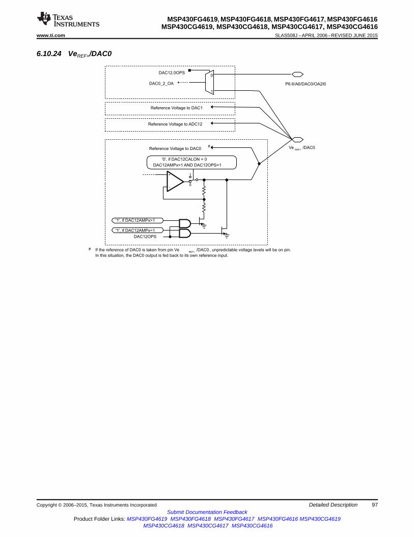
VeREF+
/DAC0
#
Reference Voltage to ADC12
1
0
'0', if DAC12CALON = 0
DAC12AMPx>1 AND DAC12OPS=1
'1', if DAC12AMPx=1
'1', if DAC12AMPx>1
+
-
DAC12OPS
Reference Voltage to DAC1
Reference Voltage to DAC0
If the reference of DAC0 is taken from pin VeREF+
/DAC0 , unpredictable voltage levels will be on pin.
In this situation, the DAC0 output is fed back to its own reference input.
#
DAC0_2_OA
DAC12.0OPS
1
0
P6.6/A6/DAC0/OA2I0
MSP430FG4619, MSP430FG4618, MSP430FG4617, MSP430FG4616MSP430CG4619, MSP430CG4618, MSP430CG4617, MSP430CG4616
www.ti.com SLAS508J –APRIL 2006–REVISED JUNE 2015
6.10.24 VeREF+/DAC0
Copyright © 2006–2015, Texas Instruments Incorporated Detailed Description 97Submit Documentation Feedback
Product Folder Links: MSP430FG4619 MSP430FG4618 MSP430FG4617 MSP430FG4616 MSP430CG4619MSP430CG4618 MSP430CG4617 MSP430CG4616

TDI
TDO
TMS
TDI/TCLK
TDO/TDI
Controlled
by JTAG
TCK
TMS
TCK
DVCC
Controlled by JTAG
Test
JTAG
and
Emulation
Module
DVCC
DVCC
Burn and Test
Fuse
RST/NMI
G
D
SU
G
D
SUTCK
Tau ~ 50 ns
Brownout
Controlled by JTAG
MSP430FG4619, MSP430FG4618, MSP430FG4617, MSP430FG4616MSP430CG4619, MSP430CG4618, MSP430CG4617, MSP430CG4616SLAS508J –APRIL 2006–REVISED JUNE 2015 www.ti.com
6.10.25 JTAG Pins TMS, TCK, TDI/TCLK, TDO/TDI, Input/Output With Schmitt Trigger or Output
98 Detailed Description Copyright © 2006–2015, Texas Instruments IncorporatedSubmit Documentation Feedback
Product Folder Links: MSP430FG4619 MSP430FG4618 MSP430FG4617 MSP430FG4616 MSP430CG4619MSP430CG4618 MSP430CG4617 MSP430CG4616

Time TMS Goes Low After POR
TMS
I(TF)
ITDI/TCLK
MSP430FG4619, MSP430FG4618, MSP430FG4617, MSP430FG4616MSP430CG4619, MSP430CG4618, MSP430CG4617, MSP430CG4616
www.ti.com SLAS508J –APRIL 2006–REVISED JUNE 2015
6.10.26 JTAG Fuse Check ModeDevices that have the fuse on the TDI/TCLK terminal have a fuse check mode that tests the continuity ofthe fuse the first time the JTAG port is accessed after a power-on reset (POR). When activated, a fusecheck current (I(TF)) of 1 mA at 3 V can flow from the TDI/TCLK pin to ground if the fuse is not burned.Care must be taken to avoid accidentally activating the fuse check mode and increasing overall systempower consumption.
Activation of the fuse check mode occurs with the first negative edge on the TMS pin after power up or ifthe TMS is being held low during power up. The second positive edge on the TMS pin deactivates thefuse check mode. After deactivation, the fuse check mode remains inactive until another POR occurs.After each POR the fuse check mode has the potential to be activated.
The fuse check current only flows when the fuse check mode is active and the TMS pin is in a low state(see Figure 6-1). Therefore, the additional current flow can be prevented by holding the TMS pin high(default condition). The JTAG pins are terminated internally and therefore do not require externaltermination.
Figure 6-1. Fuse Check Mode Current
Copyright © 2006–2015, Texas Instruments Incorporated Detailed Description 99Submit Documentation Feedback
Product Folder Links: MSP430FG4619 MSP430FG4618 MSP430FG4617 MSP430FG4616 MSP430CG4619MSP430CG4618 MSP430CG4617 MSP430CG4616
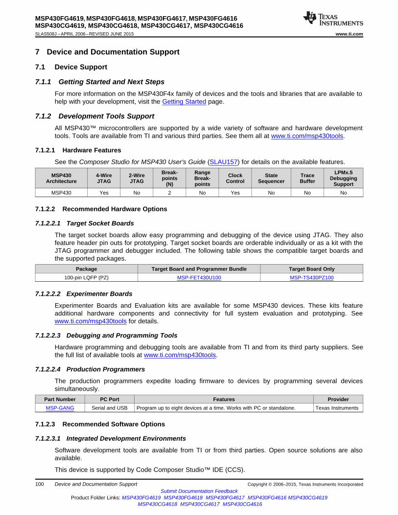
MSP430FG4619, MSP430FG4618, MSP430FG4617, MSP430FG4616MSP430CG4619, MSP430CG4618, MSP430CG4617, MSP430CG4616SLAS508J –APRIL 2006–REVISED JUNE 2015 www.ti.com
7 Device and Documentation Support
7.1 Device Support
7.1.1 Getting Started and Next StepsFor more information on the MSP430F4x family of devices and the tools and libraries that are available tohelp with your development, visit the Getting Started page.
7.1.2 Development Tools SupportAll MSP430™ microcontrollers are supported by a wide variety of software and hardware developmenttools. Tools are available from TI and various third parties. See them all at www.ti.com/msp430tools.
7.1.2.1 Hardware Features
See the Composer Studio for MSP430 User's Guide (SLAU157) for details on the available features.Break- Range LPMx.5MSP430 4-Wire 2-Wire Clock State Tracepoints Break- DebuggingArchitecture JTAG JTAG Control Sequencer Buffer(N) points Support
MSP430 Yes No 2 No Yes No No No
7.1.2.2 Recommended Hardware Options
7.1.2.2.1 Target Socket Boards
The target socket boards allow easy programming and debugging of the device using JTAG. They alsofeature header pin outs for prototyping. Target socket boards are orderable individually or as a kit with theJTAG programmer and debugger included. The following table shows the compatible target boards andthe supported packages.
Package Target Board and Programmer Bundle Target Board Only100-pin LQFP (PZ) MSP-FET430U100 MSP-TS430PZ100
7.1.2.2.2 Experimenter Boards
Experimenter Boards and Evaluation kits are available for some MSP430 devices. These kits featureadditional hardware components and connectivity for full system evaluation and prototyping. Seewww.ti.com/msp430tools for details.
7.1.2.2.3 Debugging and Programming Tools
Hardware programming and debugging tools are available from TI and from its third party suppliers. Seethe full list of available tools at www.ti.com/msp430tools.
7.1.2.2.4 Production Programmers
The production programmers expedite loading firmware to devices by programming several devicessimultaneously.
Part Number PC Port Features ProviderMSP-GANG Serial and USB Program up to eight devices at a time. Works with PC or standalone. Texas Instruments
7.1.2.3 Recommended Software Options
7.1.2.3.1 Integrated Development Environments
Software development tools are available from TI or from third parties. Open source solutions are alsoavailable.
This device is supported by Code Composer Studio™ IDE (CCS).
100 Device and Documentation Support Copyright © 2006–2015, Texas Instruments IncorporatedSubmit Documentation Feedback
Product Folder Links: MSP430FG4619 MSP430FG4618 MSP430FG4617 MSP430FG4616 MSP430CG4619MSP430CG4618 MSP430CG4617 MSP430CG4616

MSP430FG4619, MSP430FG4618, MSP430FG4617, MSP430FG4616MSP430CG4619, MSP430CG4618, MSP430CG4617, MSP430CG4616
www.ti.com SLAS508J –APRIL 2006–REVISED JUNE 2015
7.1.2.3.2 MSP430Ware
MSP430Ware is a collection of code examples, data sheets, and other design resources for all MSP430devices delivered in a convenient package. In addition to providing a complete collection of existingMSP430 design resources, MSP430Ware also includes a high-level API called MSP430 Driver Library.This library makes it easy to program MSP430 hardware. MSP430Ware is available as a component ofCCS or as a standalone package.
7.1.2.3.3 Command-Line Programmer
MSP430 Flasher is an open-source shell-based interface for programming MSP430 microcontrollersthrough a FET programmer or eZ430 using JTAG or Spy-Bi-Wire (SBW) communication. MSP430 Flashercan be used to download binary files (.txt or .hex) files directly to the MSP430 microcontroller without theneed for an IDE.
7.1.3 Device and Development Tool NomenclatureTo designate the stages in the product development cycle, TI assigns prefixes to the part numbers of allMSP430 MCU devices and support tools. Each MSP430 MCU commercial family member has one ofthree prefixes: MSP, PMS, or XMS (for example, MSP430F5438A). TI recommends two of three possibleprefix designators for its support tools: MSP and MSPX. These prefixes represent evolutionary stages ofproduct development from engineering prototypes (with XMS for devices and MSPX for tools) through fullyqualified production devices and tools (with MSP for devices and MSP for tools).
Device development evolutionary flow:
XMS – Experimental device that is not necessarily representative of the electrical specifications for thefinal device
PMS – Final silicon die that conforms to the electrical specifications for the device but has not completedquality and reliability verification
MSP – Fully qualified production device
Support tool development evolutionary flow:
MSPX – Development-support product that has not yet completed TI's internal qualification testing.
MSP – Fully-qualified development-support product
XMS and PMS devices and MSPX development-support tools are shipped against the followingdisclaimer:
"Developmental product is intended for internal evaluation purposes."
MSP devices and MSP development-support tools have been characterized fully, and the quality andreliability of the device have been demonstrated fully. TI's standard warranty applies.
Predictions show that prototype devices (XMS and PMS) have a greater failure rate than the standardproduction devices. TI recommends that these devices not be used in any production system becausetheir expected end-use failure rate still is undefined. Only qualified production devices are to be used.
TI device nomenclature also includes a suffix with the device family name. This suffix indicates thepackage type (for example, PZP) and temperature range (for example, T). Figure 7-1 provides a legendfor reading the complete device name for any family member.
Copyright © 2006–2015, Texas Instruments Incorporated Device and Documentation Support 101Submit Documentation Feedback
Product Folder Links: MSP430FG4619 MSP430FG4618 MSP430FG4617 MSP430FG4616 MSP430CG4619MSP430CG4618 MSP430CG4617 MSP430CG4616

Processor Family CC = Embedded RF RadioMSP = Mixed-Signal ProcessorXMS = Experimental SiliconPMS = Prototype Device
430 MCU Platform TI’s Low-Power Microcontroller Platform
Device Type Memory TypeC = ROMF = FlashFR = FRAMG = Flash or FRAM (Value Line)L = No Nonvolatile Memory
Specialized ApplicationAFE = Analog Front EndBT = Preprogrammed withBQ = Contactless PowerCG = ROM MedicalFE = Flash Energy MeterFG = Flash MedicalFW = Flash Electronic Flow Meter
Bluetooth
Series 1 Series = Up to 8 MHz2 Series = Up to 16 MHz3 Series = Legacy4 Series = Up to 16 MHz with LCD
5 Series = Up to 25 MHz6 Series = Up to 25 MHz with LCD0 = Low-Voltage Series
Feature Set Various Levels of Integration Within a Series
Optional: A = Revision N/A
Optional: Temperature Range S = 0°C to 50 CC to 70 C
I = 40 C to 85 CT = –40 C to 105 C
°C = 0° °
– ° °° °
Packaging http://www.ti.com/packaging
Optional: Tape and Reel T = Small ReelR = Large ReelNo Markings = Tube or Tray
Optional: Additional Features -EP = Enhanced Product ( 40°C to 105°C)-HT = Extreme Temperature Parts ( 55°C to 150°C)-Q1 = Automotive Q100 Qualified
––
MSP 430 F 5 438 A I ZQW T XX
Processor Family
Series Optional: Temperature Range
430 MCU Platform
PackagingDevice Type
Optional: A = Revision
Optional: Tape and Reel
Feature Set
Optional: Additional Features
MSP430FG4619, MSP430FG4618, MSP430FG4617, MSP430FG4616MSP430CG4619, MSP430CG4618, MSP430CG4617, MSP430CG4616SLAS508J –APRIL 2006–REVISED JUNE 2015 www.ti.com
Figure 7-1. Device Nomenclature
102 Device and Documentation Support Copyright © 2006–2015, Texas Instruments IncorporatedSubmit Documentation Feedback
Product Folder Links: MSP430FG4619 MSP430FG4618 MSP430FG4617 MSP430FG4616 MSP430CG4619MSP430CG4618 MSP430CG4617 MSP430CG4616

MSP430FG4619, MSP430FG4618, MSP430FG4617, MSP430FG4616MSP430CG4619, MSP430CG4618, MSP430CG4617, MSP430CG4616
www.ti.com SLAS508J –APRIL 2006–REVISED JUNE 2015
7.2 Documentation SupportThe following documents describe the MSP430FG461x and MSP430CG461x devices. Copies of thesedocuments are available on the Internet at www.ti.com.
SLAU056 MSP430F4xx Family User's Guide. Detailed information on the modules and peripheralsavailable in this device family.
SLAZ369 MSP430FG4619 Device Erratasheet. Describes the known exceptions to the functionalspecifications for all silicon revisions of the device.
SLAZ368 MSP430FG4618 Device Erratasheet. Describes the known exceptions to the functionalspecifications for all silicon revisions of the device.
SLAZ367 MSP430FG4617 Device Erratasheet. Describes the known exceptions to the functionalspecifications for all silicon revisions of the device.
SLAZ366 MSP430FG4616 Device Erratasheet. Describes the known exceptions to the functionalspecifications for all silicon revisions of the device.
SLAZ123 MSP430CG4619 Device Erratasheet. Describes the known exceptions to the functionalspecifications for all silicon revisions of the device.
SLAZ122 MSP430CG4618 Device Erratasheet. Describes the known exceptions to the functionalspecifications for all silicon revisions of the device.
SLAZ121 MSP430CG4617 Device Erratasheet. Describes the known exceptions to the functionalspecifications for all silicon revisions of the device.
SLAZ120 MSP430CG4616 Device Erratasheet. Describes the known exceptions to the functionalspecifications for all silicon revisions of the device.
7.3 Related LinksTable 7-1 lists quick access links. Categories include technical documents, support and communityresources, tools and software, and quick access to sample or buy.
Table 7-1. Related Links
TECHNICAL TOOLS & SUPPORT &PARTS PRODUCT FOLDER SAMPLE & BUY DOCUMENTS SOFTWARE COMMUNITYMSP430FG4619 Click here Click here Click here Click here Click hereMSP430FG4618 Click here Click here Click here Click here Click hereMSP430FG4617 Click here Click here Click here Click here Click hereMSP430FG4616 Click here Click here Click here Click here Click hereMSP430CG4619 Click here Click here Click here Click here Click hereMSP430CG4618 Click here Click here Click here Click here Click hereMSP430CG4617 Click here Click here Click here Click here Click hereMSP430CG4616 Click here Click here Click here Click here Click here
Copyright © 2006–2015, Texas Instruments Incorporated Device and Documentation Support 103Submit Documentation Feedback
Product Folder Links: MSP430FG4619 MSP430FG4618 MSP430FG4617 MSP430FG4616 MSP430CG4619MSP430CG4618 MSP430CG4617 MSP430CG4616

MSP430FG4619, MSP430FG4618, MSP430FG4617, MSP430FG4616MSP430CG4619, MSP430CG4618, MSP430CG4617, MSP430CG4616SLAS508J –APRIL 2006–REVISED JUNE 2015 www.ti.com
7.4 Community ResourcesThe following links connect to TI community resources. Linked contents are provided "AS IS" by therespective contributors. They do not constitute TI specifications and do not necessarily reflect TI's views;see TI's Terms of Use.
TI E2E™ CommunityTI's Engineer-to-Engineer (E2E) Community. Created to foster collaboration among engineers. Ate2e.ti.com, you can ask questions, share knowledge, explore ideas, and help solve problems with fellowengineers.
TI Embedded Processors WikiTexas Instruments Embedded Processors Wiki. Established to help developers get started with embeddedprocessors from Texas Instruments and to foster innovation and growth of general knowledge about thehardware and software surrounding these devices.
7.5 TrademarksMSP430, MicroStar Junior, Code Composer Studio, E2E are trademarks of Texas Instruments.
7.6 Electrostatic Discharge CautionThis integrated circuit can be damaged by ESD. Texas Instruments recommends that all integrated circuits be handled withappropriate precautions. Failure to observe proper handling and installation procedures can cause damage.
ESD damage can range from subtle performance degradation to complete device failure. Precision integrated circuits may be moresusceptible to damage because very small parametric changes could cause the device not to meet its published specifications.
7.7 Export Control NoticeRecipient agrees to not knowingly export or re-export, directly or indirectly, any product or technical data(as defined by the U.S., EU, and other Export Administration Regulations) including software, or anycontrolled product restricted by other applicable national regulations, received from disclosing party undernondisclosure obligations (if any), or any direct product of such technology, to any destination to whichsuch export or re-export is restricted or prohibited by U.S. or other applicable laws, without obtaining priorauthorization from U.S. Department of Commerce and other competent Government authorities to theextent required by those laws.
7.8 GlossarySLYZ022 — TI Glossary.
This glossary lists and explains terms, acronyms, and definitions.
104 Device and Documentation Support Copyright © 2006–2015, Texas Instruments IncorporatedSubmit Documentation Feedback
Product Folder Links: MSP430FG4619 MSP430FG4618 MSP430FG4617 MSP430FG4616 MSP430CG4619MSP430CG4618 MSP430CG4617 MSP430CG4616

MSP430FG4619, MSP430FG4618, MSP430FG4617, MSP430FG4616MSP430CG4619, MSP430CG4618, MSP430CG4617, MSP430CG4616
www.ti.com SLAS508J –APRIL 2006–REVISED JUNE 2015
8 Mechanical, Packaging, and Orderable Information
The following pages include mechanical, packaging, and orderable information. This information is themost current data available for the designated devices. This data is subject to change without notice andrevision of this document. For browser-based versions of this data sheet, refer to the left-hand navigation.
Copyright © 2006–2015, Texas Instruments Incorporated Mechanical, Packaging, and Orderable Information 105Submit Documentation Feedback
Product Folder Links: MSP430FG4619 MSP430FG4618 MSP430FG4617 MSP430FG4616 MSP430CG4619MSP430CG4618 MSP430CG4617 MSP430CG4616

PACKAGE OPTION ADDENDUM
www.ti.com 31-May-2017
Addendum-Page 1
PACKAGING INFORMATION
Orderable Device Status(1)
Package Type PackageDrawing
Pins PackageQty
Eco Plan(2)
Lead/Ball Finish(6)
MSL Peak Temp(3)
Op Temp (°C) Device Marking(4/5)
Samples
MSP430FG4616IPZ ACTIVE LQFP PZ 100 90 Green (RoHS& no Sb/Br)
CU NIPDAU Level-3-260C-168 HR -40 to 85 M430FG4616
MSP430FG4616IPZR ACTIVE LQFP PZ 100 1000 Green (RoHS& no Sb/Br)
CU NIPDAU Level-3-260C-168 HR -40 to 85 M430FG4616
MSP430FG4616IZQW ACTIVE BGAMICROSTAR
JUNIOR
ZQW 113 250 Green (RoHS& no Sb/Br)
SNAGCU Level-3-260C-168 HR -40 to 85 M430FG4616
MSP430FG4616IZQWR ACTIVE BGAMICROSTAR
JUNIOR
ZQW 113 2500 Green (RoHS& no Sb/Br)
SNAGCU Level-3-260C-168 HR -40 to 85 M430FG4616
MSP430FG4617IPZ ACTIVE LQFP PZ 100 90 Green (RoHS& no Sb/Br)
CU NIPDAU Level-3-260C-168 HR -40 to 85 M430FG4617
MSP430FG4617IPZR ACTIVE LQFP PZ 100 1000 Green (RoHS& no Sb/Br)
CU NIPDAU Level-3-260C-168 HR -40 to 85 M430FG4617
MSP430FG4617IZQWR ACTIVE BGAMICROSTAR
JUNIOR
ZQW 113 2500 Green (RoHS& no Sb/Br)
SNAGCU Level-3-260C-168 HR -40 to 85 M430FG4617
MSP430FG4618IPZ ACTIVE LQFP PZ 100 90 Green (RoHS& no Sb/Br)
CU NIPDAU Level-3-260C-168 HR -40 to 85 M430FG4618
MSP430FG4618IPZR ACTIVE LQFP PZ 100 1000 Green (RoHS& no Sb/Br)
CU NIPDAU Level-3-260C-168 HR -40 to 85 M430FG4618
MSP430FG4618IZQW ACTIVE BGAMICROSTAR
JUNIOR
ZQW 113 250 Green (RoHS& no Sb/Br)
SNAGCU Level-3-260C-168 HR -40 to 85 M430FG4618
MSP430FG4618IZQWR ACTIVE BGAMICROSTAR
JUNIOR
ZQW 113 2500 Green (RoHS& no Sb/Br)
SNAGCU Level-3-260C-168 HR -40 to 85 M430FG4618
MSP430FG4618IZQWT ACTIVE BGAMICROSTAR
JUNIOR
ZQW 113 250 Green (RoHS& no Sb/Br)
SNAGCU Level-3-260C-168 HR M430FG4618
MSP430FG4619IPZ ACTIVE LQFP PZ 100 90 Green (RoHS& no Sb/Br)
CU NIPDAU Level-3-260C-168 HR -40 to 85 M430FG4619REV #
MSP430FG4619IPZR ACTIVE LQFP PZ 100 1000 Green (RoHS& no Sb/Br)
CU NIPDAU Level-3-260C-168 HR -40 to 85 M430FG4619

PACKAGE OPTION ADDENDUM
www.ti.com 31-May-2017
Addendum-Page 2
Orderable Device Status(1)
Package Type PackageDrawing
Pins PackageQty
Eco Plan(2)
Lead/Ball Finish(6)
MSL Peak Temp(3)
Op Temp (°C) Device Marking(4/5)
Samples
MSP430FG4619IZQW ACTIVE BGAMICROSTAR
JUNIOR
ZQW 113 250 Green (RoHS& no Sb/Br)
SNAGCU Level-3-260C-168 HR -40 to 85 M430FG4619
MSP430FG4619IZQWR ACTIVE BGAMICROSTAR
JUNIOR
ZQW 113 2500 Green (RoHS& no Sb/Br)
SNAGCU Level-3-260C-168 HR -40 to 85 M430FG4619
MSP430FG4619IZQWT ACTIVE BGAMICROSTAR
JUNIOR
ZQW 113 250 Green (RoHS& no Sb/Br)
SNAGCU Level-3-260C-168 HR -40 to 85 M430FG4619
(1) The marketing status values are defined as follows:ACTIVE: Product device recommended for new designs.LIFEBUY: TI has announced that the device will be discontinued, and a lifetime-buy period is in effect.NRND: Not recommended for new designs. Device is in production to support existing customers, but TI does not recommend using this part in a new design.PREVIEW: Device has been announced but is not in production. Samples may or may not be available.OBSOLETE: TI has discontinued the production of the device.
(2) RoHS: TI defines "RoHS" to mean semiconductor products that are compliant with the current EU RoHS requirements for all 10 RoHS substances, including the requirement that RoHS substancedo not exceed 0.1% by weight in homogeneous materials. Where designed to be soldered at high temperatures, "RoHS" products are suitable for use in specified lead-free processes. TI mayreference these types of products as "Pb-Free".RoHS Exempt: TI defines "RoHS Exempt" to mean products that contain lead but are compliant with EU RoHS pursuant to a specific EU RoHS exemption.Green: TI defines "Green" to mean the content of Chlorine (Cl) and Bromine (Br) based flame retardants meet JS709B low halogen requirements of <=1000ppm threshold. Antimony trioxide basedflame retardants must also meet the <=1000ppm threshold requirement.
(3) MSL, Peak Temp. - The Moisture Sensitivity Level rating according to the JEDEC industry standard classifications, and peak solder temperature.
(4) There may be additional marking, which relates to the logo, the lot trace code information, or the environmental category on the device.
(5) Multiple Device Markings will be inside parentheses. Only one Device Marking contained in parentheses and separated by a "~" will appear on a device. If a line is indented then it is a continuationof the previous line and the two combined represent the entire Device Marking for that device.
(6) Lead/Ball Finish - Orderable Devices may have multiple material finish options. Finish options are separated by a vertical ruled line. Lead/Ball Finish values may wrap to two lines if the finishvalue exceeds the maximum column width.
Important Information and Disclaimer:The information provided on this page represents TI's knowledge and belief as of the date that it is provided. TI bases its knowledge and belief on informationprovided by third parties, and makes no representation or warranty as to the accuracy of such information. Efforts are underway to better integrate information from third parties. TI has taken andcontinues to take reasonable steps to provide representative and accurate information but may not have conducted destructive testing or chemical analysis on incoming materials and chemicals.TI and TI suppliers consider certain information to be proprietary, and thus CAS numbers and other limited information may not be available for release.

PACKAGE OPTION ADDENDUM
www.ti.com 31-May-2017
Addendum-Page 3
In no event shall TI's liability arising out of such information exceed the total purchase price of the TI part(s) at issue in this document sold by TI to Customer on an annual basis.
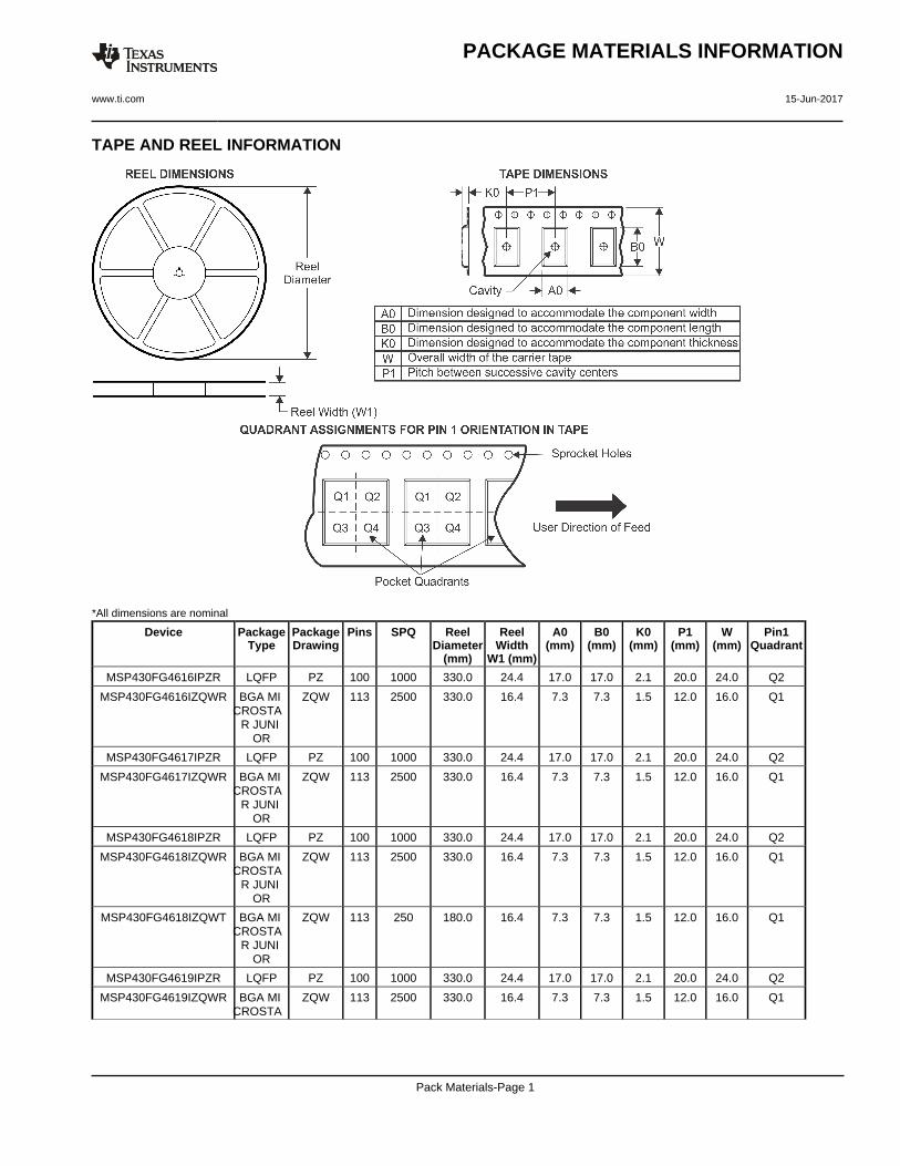
TAPE AND REEL INFORMATION
*All dimensions are nominal
Device PackageType
PackageDrawing
Pins SPQ ReelDiameter
(mm)
ReelWidth
W1 (mm)
A0(mm)
B0(mm)
K0(mm)
P1(mm)
W(mm)
Pin1Quadrant
MSP430FG4616IPZR LQFP PZ 100 1000 330.0 24.4 17.0 17.0 2.1 20.0 24.0 Q2
MSP430FG4616IZQWR BGA MI CROSTA
R JUNI OR
ZQW 113 2500 330.0 16.4 7.3 7.3 1.5 12.0 16.0 Q1
MSP430FG4617IPZR LQFP PZ 100 1000 330.0 24.4 17.0 17.0 2.1 20.0 24.0 Q2
MSP430FG4617IZQWR BGA MI CROSTA
R JUNI OR
ZQW 113 2500 330.0 16.4 7.3 7.3 1.5 12.0 16.0 Q1
MSP430FG4618IPZR LQFP PZ 100 1000 330.0 24.4 17.0 17.0 2.1 20.0 24.0 Q2
MSP430FG4618IZQWR BGA MI CROSTA
R JUNI OR
ZQW 113 2500 330.0 16.4 7.3 7.3 1.5 12.0 16.0 Q1
MSP430FG4618IZQWT BGA MI CROSTA
R JUNI OR
ZQW 113 250 180.0 16.4 7.3 7.3 1.5 12.0 16.0 Q1
MSP430FG4619IPZR LQFP PZ 100 1000 330.0 24.4 17.0 17.0 2.1 20.0 24.0 Q2
MSP430FG4619IZQWR BGA MI CROSTA
ZQW 113 2500 330.0 16.4 7.3 7.3 1.5 12.0 16.0 Q1
PACKAGE MATERIALS INFORMATION
www.ti.com 15-Jun-2017
Pack Materials-Page 1

Device PackageType
PackageDrawing
Pins SPQ ReelDiameter
(mm)
ReelWidth
W1 (mm)
A0(mm)
B0(mm)
K0(mm)
P1(mm)
W(mm)
Pin1Quadrant
R JUNI OR
MSP430FG4619IZQWT BGA MI CROSTA
R JUNI OR
ZQW 113 250 180.0 16.4 7.3 7.3 1.5 12.0 16.0 Q1
*All dimensions are nominal
Device Package Type Package Drawing Pins SPQ Length (mm) Width (mm) Height (mm)
MSP430FG4616IPZR LQFP PZ 100 1000 367.0 367.0 45.0
MSP430FG4616IZQWR BGA MICROSTARJUNIOR
ZQW 113 2500 336.6 336.6 28.6
MSP430FG4617IPZR LQFP PZ 100 1000 367.0 367.0 45.0
MSP430FG4617IZQWR BGA MICROSTARJUNIOR
ZQW 113 2500 336.6 336.6 28.6
MSP430FG4618IPZR LQFP PZ 100 1000 367.0 367.0 45.0
MSP430FG4618IZQWR BGA MICROSTARJUNIOR
ZQW 113 2500 336.6 336.6 28.6
MSP430FG4618IZQWT BGA MICROSTARJUNIOR
ZQW 113 250 213.0 191.0 55.0
MSP430FG4619IPZR LQFP PZ 100 1000 367.0 367.0 45.0
MSP430FG4619IZQWR BGA MICROSTAR ZQW 113 2500 336.6 336.6 28.6
PACKAGE MATERIALS INFORMATION
www.ti.com 15-Jun-2017
Pack Materials-Page 2

Device Package Type Package Drawing Pins SPQ Length (mm) Width (mm) Height (mm)
JUNIOR
MSP430FG4619IZQWT BGA MICROSTARJUNIOR
ZQW 113 250 213.0 191.0 55.0
PACKAGE MATERIALS INFORMATION
www.ti.com 15-Jun-2017
Pack Materials-Page 3

MECHANICAL DATA
MTQF013A – OCTOBER 1994 – REVISED DECEMBER 1996
1POST OFFICE BOX 655303 • DALLAS, TEXAS 75265
PZ (S-PQFP-G100) PLASTIC QUAD FLATPACK
4040149/B 11/96
50
26 0,13 NOM
Gage Plane
0,25
0,450,75
0,05 MIN
0,27
51
25
75
1
12,00 TYP
0,17
76
100
SQ
SQ15,8016,20
13,80
1,351,45
1,60 MAX
14,20
0°–7°
Seating Plane
0,08
0,50 M0,08
NOTES: A. All linear dimensions are in millimeters.B. This drawing is subject to change without notice.C. Falls within JEDEC MS-026

IMPORTANT NOTICE
Texas Instruments Incorporated (TI) reserves the right to make corrections, enhancements, improvements and other changes to itssemiconductor products and services per JESD46, latest issue, and to discontinue any product or service per JESD48, latest issue. Buyersshould obtain the latest relevant information before placing orders and should verify that such information is current and complete.TI’s published terms of sale for semiconductor products (http://www.ti.com/sc/docs/stdterms.htm) apply to the sale of packaged integratedcircuit products that TI has qualified and released to market. Additional terms may apply to the use or sale of other types of TI products andservices.Reproduction of significant portions of TI information in TI data sheets is permissible only if reproduction is without alteration and isaccompanied by all associated warranties, conditions, limitations, and notices. TI is not responsible or liable for such reproduceddocumentation. Information of third parties may be subject to additional restrictions. Resale of TI products or services with statementsdifferent from or beyond the parameters stated by TI for that product or service voids all express and any implied warranties for theassociated TI product or service and is an unfair and deceptive business practice. TI is not responsible or liable for any such statements.Buyers and others who are developing systems that incorporate TI products (collectively, “Designers”) understand and agree that Designersremain responsible for using their independent analysis, evaluation and judgment in designing their applications and that Designers havefull and exclusive responsibility to assure the safety of Designers' applications and compliance of their applications (and of all TI productsused in or for Designers’ applications) with all applicable regulations, laws and other applicable requirements. Designer represents that, withrespect to their applications, Designer has all the necessary expertise to create and implement safeguards that (1) anticipate dangerousconsequences of failures, (2) monitor failures and their consequences, and (3) lessen the likelihood of failures that might cause harm andtake appropriate actions. Designer agrees that prior to using or distributing any applications that include TI products, Designer willthoroughly test such applications and the functionality of such TI products as used in such applications.TI’s provision of technical, application or other design advice, quality characterization, reliability data or other services or information,including, but not limited to, reference designs and materials relating to evaluation modules, (collectively, “TI Resources”) are intended toassist designers who are developing applications that incorporate TI products; by downloading, accessing or using TI Resources in anyway, Designer (individually or, if Designer is acting on behalf of a company, Designer’s company) agrees to use any particular TI Resourcesolely for this purpose and subject to the terms of this Notice.TI’s provision of TI Resources does not expand or otherwise alter TI’s applicable published warranties or warranty disclaimers for TIproducts, and no additional obligations or liabilities arise from TI providing such TI Resources. TI reserves the right to make corrections,enhancements, improvements and other changes to its TI Resources. TI has not conducted any testing other than that specificallydescribed in the published documentation for a particular TI Resource.Designer is authorized to use, copy and modify any individual TI Resource only in connection with the development of applications thatinclude the TI product(s) identified in such TI Resource. NO OTHER LICENSE, EXPRESS OR IMPLIED, BY ESTOPPEL OR OTHERWISETO ANY OTHER TI INTELLECTUAL PROPERTY RIGHT, AND NO LICENSE TO ANY TECHNOLOGY OR INTELLECTUAL PROPERTYRIGHT OF TI OR ANY THIRD PARTY IS GRANTED HEREIN, including but not limited to any patent right, copyright, mask work right, orother intellectual property right relating to any combination, machine, or process in which TI products or services are used. Informationregarding or referencing third-party products or services does not constitute a license to use such products or services, or a warranty orendorsement thereof. Use of TI Resources may require a license from a third party under the patents or other intellectual property of thethird party, or a license from TI under the patents or other intellectual property of TI.TI RESOURCES ARE PROVIDED “AS IS” AND WITH ALL FAULTS. TI DISCLAIMS ALL OTHER WARRANTIES ORREPRESENTATIONS, EXPRESS OR IMPLIED, REGARDING RESOURCES OR USE THEREOF, INCLUDING BUT NOT LIMITED TOACCURACY OR COMPLETENESS, TITLE, ANY EPIDEMIC FAILURE WARRANTY AND ANY IMPLIED WARRANTIES OFMERCHANTABILITY, FITNESS FOR A PARTICULAR PURPOSE, AND NON-INFRINGEMENT OF ANY THIRD PARTY INTELLECTUALPROPERTY RIGHTS. TI SHALL NOT BE LIABLE FOR AND SHALL NOT DEFEND OR INDEMNIFY DESIGNER AGAINST ANY CLAIM,INCLUDING BUT NOT LIMITED TO ANY INFRINGEMENT CLAIM THAT RELATES TO OR IS BASED ON ANY COMBINATION OFPRODUCTS EVEN IF DESCRIBED IN TI RESOURCES OR OTHERWISE. IN NO EVENT SHALL TI BE LIABLE FOR ANY ACTUAL,DIRECT, SPECIAL, COLLATERAL, INDIRECT, PUNITIVE, INCIDENTAL, CONSEQUENTIAL OR EXEMPLARY DAMAGES INCONNECTION WITH OR ARISING OUT OF TI RESOURCES OR USE THEREOF, AND REGARDLESS OF WHETHER TI HAS BEENADVISED OF THE POSSIBILITY OF SUCH DAMAGES.Unless TI has explicitly designated an individual product as meeting the requirements of a particular industry standard (e.g., ISO/TS 16949and ISO 26262), TI is not responsible for any failure to meet such industry standard requirements.Where TI specifically promotes products as facilitating functional safety or as compliant with industry functional safety standards, suchproducts are intended to help enable customers to design and create their own applications that meet applicable functional safety standardsand requirements. Using products in an application does not by itself establish any safety features in the application. Designers mustensure compliance with safety-related requirements and standards applicable to their applications. Designer may not use any TI products inlife-critical medical equipment unless authorized officers of the parties have executed a special contract specifically governing such use.Life-critical medical equipment is medical equipment where failure of such equipment would cause serious bodily injury or death (e.g., lifesupport, pacemakers, defibrillators, heart pumps, neurostimulators, and implantables). Such equipment includes, without limitation, allmedical devices identified by the U.S. Food and Drug Administration as Class III devices and equivalent classifications outside the U.S.TI may expressly designate certain products as completing a particular qualification (e.g., Q100, Military Grade, or Enhanced Product).Designers agree that it has the necessary expertise to select the product with the appropriate qualification designation for their applicationsand that proper product selection is at Designers’ own risk. Designers are solely responsible for compliance with all legal and regulatoryrequirements in connection with such selection.Designer will fully indemnify TI and its representatives against any damages, costs, losses, and/or liabilities arising out of Designer’s non-compliance with the terms and provisions of this Notice.
Mailing Address: Texas Instruments, Post Office Box 655303, Dallas, Texas 75265Copyright © 2017, Texas Instruments Incorporated