msp430 power solutions michael day portable power applications manager€¦ · 1 6/6/2008 1 msp430...
TRANSCRIPT
1
6/6/2008 1
MSP430 Power SolutionsMichael DayPortable Power Applications Manager
2
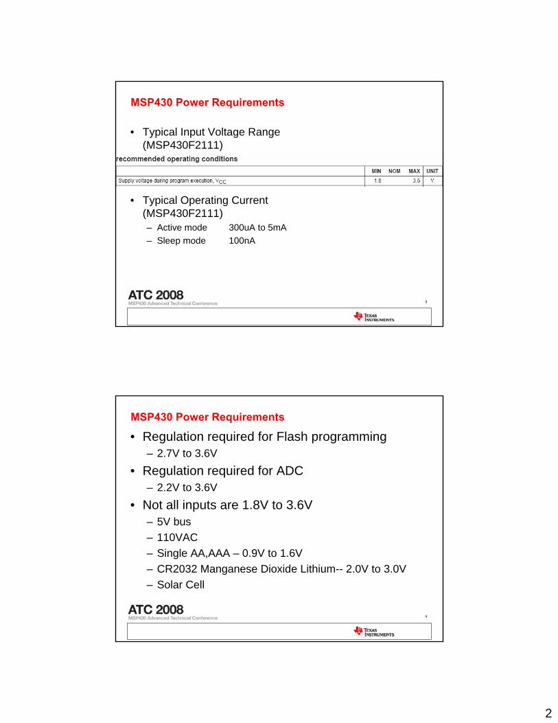
Powering the MSP430
0.5 uA
MSP430Power Supply
30uA – 5mA
2
3
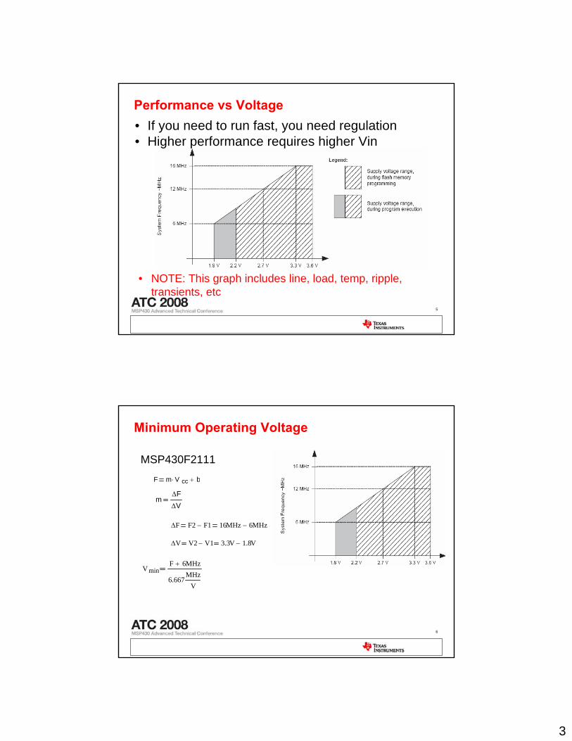
MSP430 Power Requirements
• Typical Input Voltage Range (MSP430F2111)
• Typical Operating Current (MSP430F2111)– Active mode 300uA to 5mA– Sleep mode 100nA
4
MSP430 Power Requirements
• Regulation required for Flash programming– 2.7V to 3.6V
• Regulation required for ADC– 2.2V to 3.6V
• Not all inputs are 1.8V to 3.6V– 5V bus– 110VAC– Single AA,AAA – 0.9V to 1.6V– CR2032 Manganese Dioxide Lithium-- 2.0V to 3.0V– Solar Cell
3
5
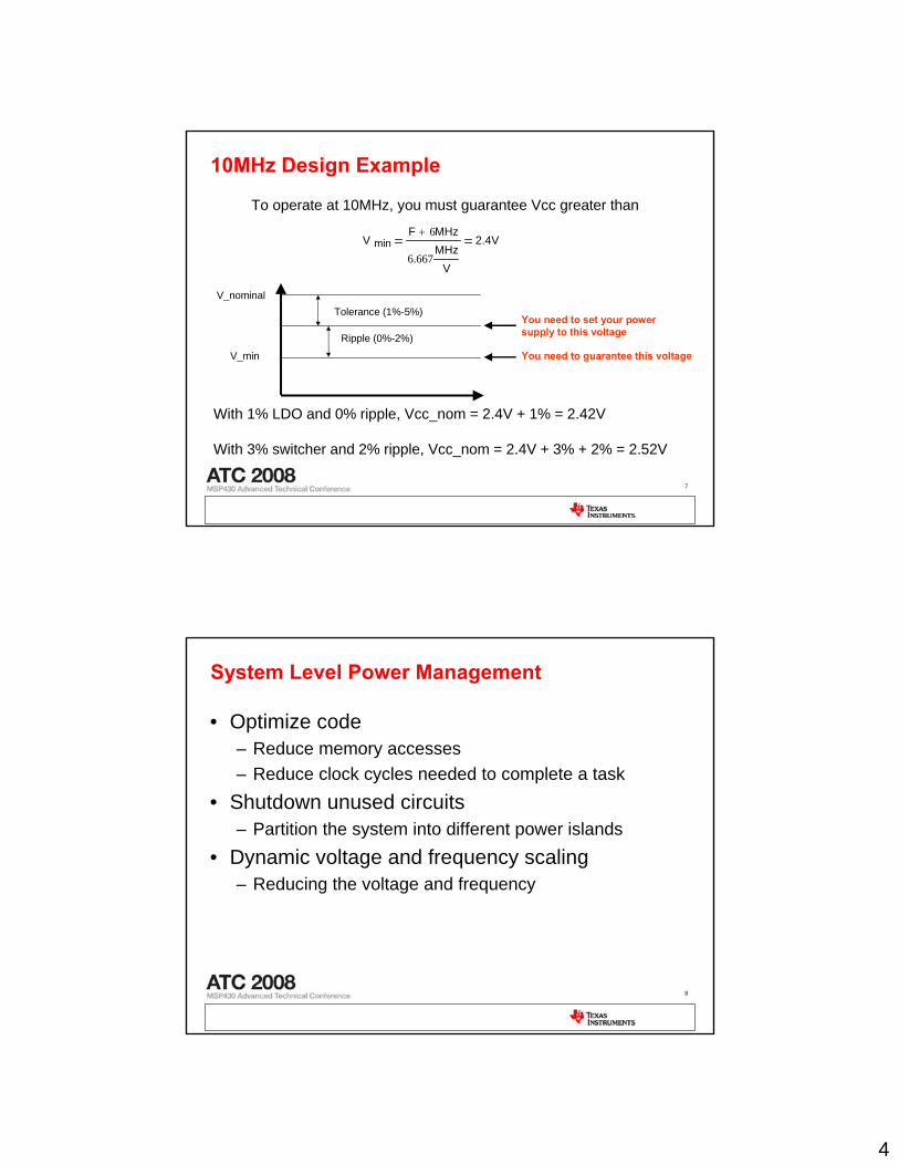
Performance vs Voltage• If you need to run fast, you need regulation• Higher performance requires higher Vin
• NOTE: This graph includes line, load, temp, ripple, transients, etc
6
Minimum Operating Voltage
ΔF F2 F1− 16MHz 6MHz−
ΔV V2 V1− 3.3V 1.8V−
V minF 6MHz+
6.667MHz
V
MSP430F2111
mΔFΔV
F m V cc⋅ b+
4
7
10MHz Design Example
V_nominalTolerance (1%-5%)
Ripple (0%-2%)
V_min You need to guarantee this voltage
You need to set your power supply to this voltage
V minF 6MHz+
6.667MHz
V
2.4V
To operate at 10MHz, you must guarantee Vcc greater than
With 1% LDO and 0% ripple, Vcc_nom = 2.4V + 1% = 2.42V
With 3% switcher and 2% ripple, Vcc_nom = 2.4V + 3% + 2% = 2.52V
8
System Level Power Management
• Optimize code– Reduce memory accesses– Reduce clock cycles needed to complete a task
• Shutdown unused circuits– Partition the system into different power islands
• Dynamic voltage and frequency scaling– Reducing the voltage and frequency
5
9
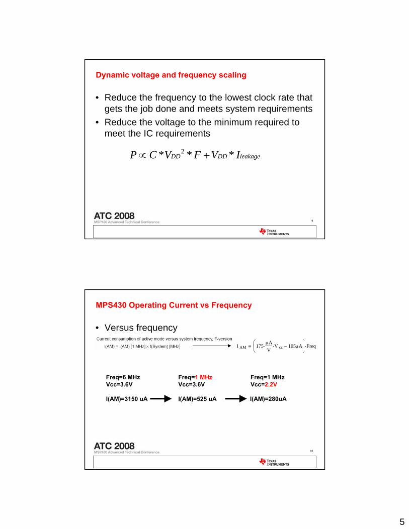
Dynamic voltage and frequency scaling
• Reduce the frequency to the lowest clock rate that gets the job done and meets system requirements
• Reduce the voltage to the minimum required to meet the IC requirements
leakageDDDD IVFVCP *** 2 +∝
10
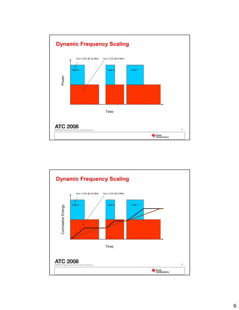
MPS430 Operating Current vs Frequency
I AM 175μAV
⋅ V cc⋅ 105μA−⎛⎜⎝
⎞⎟⎠
Freq⋅≡
Freq=1 MHzVcc=2.2V
Freq=6 MHzVcc=3.6V
I(AM)=3150 uA
Freq=1 MHzVcc=3.6V
I(AM)=525 uA I(AM)=280uA
• Versus frequency
6
11
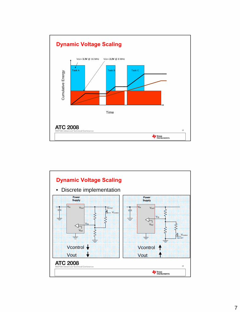
Dynamic Frequency Scaling
Pow
er
Time
Vcc= 3.3V @ 16 MHz
Task A Task B Task C
Vcc= 3.3V @ 8 MHz
12
Dynamic Frequency Scaling
Cum
ulat
ive
Ene
rgy
Time
Vcc= 3.3V @ 16 MHz
Task A Task B Task C
Vcc= 3.3V @ 8 MHz
7
13
Task CTask BTask A
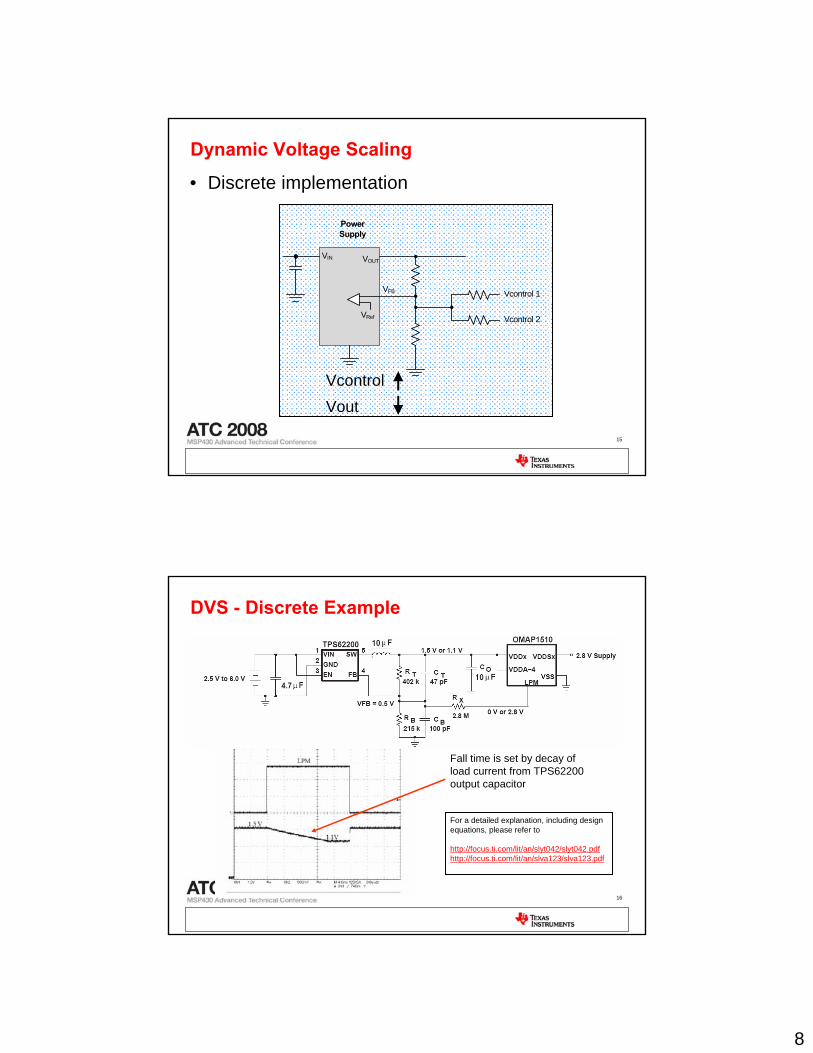
Dynamic Voltage Scaling
Cum
ulat
ive
Ene
rgy
Time
Vcc= 2.2V @ 8 MHzVcc= 3.3V @ 16 MHz
14
Dynamic Voltage Scaling
• Discrete implementation
VIN
VFB
VOUT
Power Supply
VRef
VControl
Pch FET VIN
VFB
VOUT
Power Supply
VRef
Nch FET
VControl
VcontrolVout
VcontrolVout
8
15
Dynamic Voltage Scaling
• Discrete implementation
VcontrolVout
VIN
VFB
VOUT
Power Supply
VRef
Vcontrol 1
Vcontrol 2
16
DVS - Discrete Example
Fall time is set by decay of load current from TPS62200 output capacitor
For a detailed explanation, including design equations, please refer to
http://focus.ti.com/lit/an/slyt042/slyt042.pdfhttp://focus.ti.com/lit/an/slva123/slva123.pdf
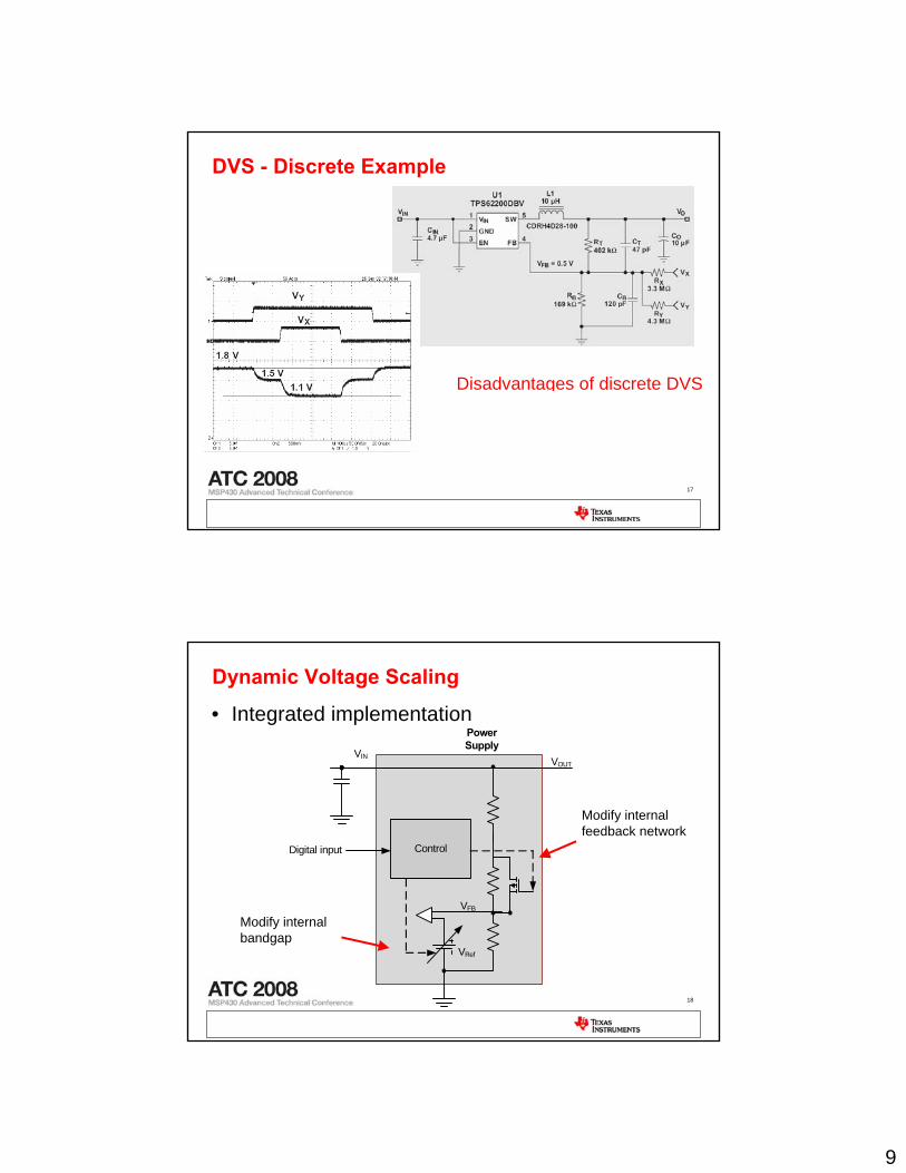
9
17
DVS - Discrete Example
Disadvantages of discrete DVSHigher parts countMore board spaceIncreased costReduced Vout Accuracy
18
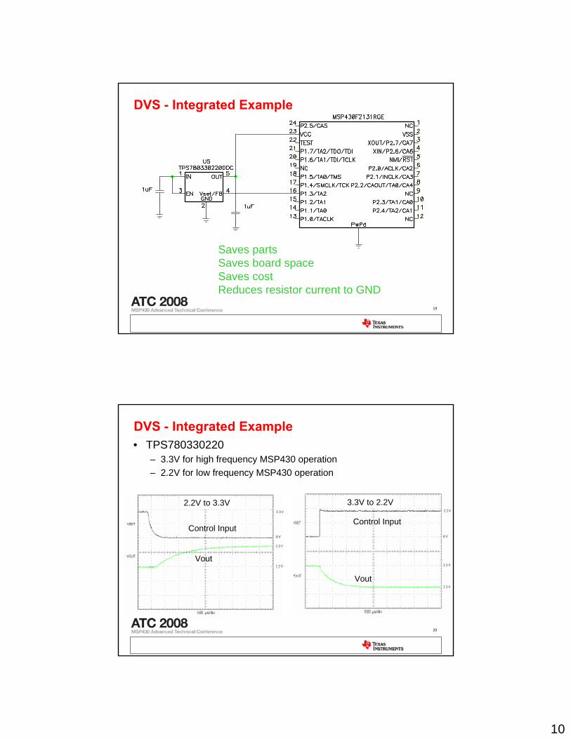
Dynamic Voltage Scaling
• Integrated implementation
VIN
VFB
VOUT
Power Supply
VRef
ControlDigital input
Modify internal feedback network
Modify internal bandgap
10
19
DVS - Integrated Example
Saves partsSaves board spaceSaves costReduces resistor current to GND
20
DVS - Integrated Example• TPS780330220
– 3.3V for high frequency MSP430 operation– 2.2V for low frequency MSP430 operation
3.3V to 2.2V2.2V to 3.3V
Control InputControl Input
Vout
Vout

11
21
DVS - Integrated
• TPS62400– Easyscale digital interface
• uP control• Internal registers• 5 bits 32 discrete output voltage setpoints
– 25mV to 100mV steps
• TPS6502x– I2C digital interface
• uP control• Internal registers• 5 bits 32 discrete output voltage setpoints
– 25mV to 300mV steps
22
Component Level Power Management
• Power Supply Efficiency– Topology (sync buck, charge pump ratio)– Component selection (inductor)– Important when operating time is long
• Quiescent current– Component selection (feedback resistors)– IC selection (quiescent/standby currents)– Important when standby times are long
12
23
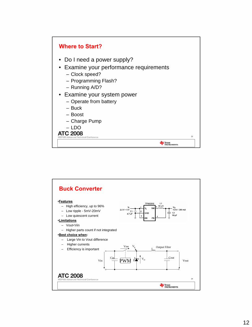
Where to Start?
• Do I need a power supply?• Examine your performance requirements
– Clock speed?– Programming Flash?– Running A/D?
• Examine your system power– Operate from battery– Buck– Boost– Charge Pump– LDO
24
Buck Converter
•Features – High efficiency, up to 96%– Low ripple - 5mV-20mV– Low quiescent current
•Limitations– Vout<Vin– Higher parts count if not integrated
•Best choice when:– Large Vin to Vout difference – Higher currents – Efficiency is important L Output FilterVLVsw
PWMCin Cout
DVin VoutVD
13
25
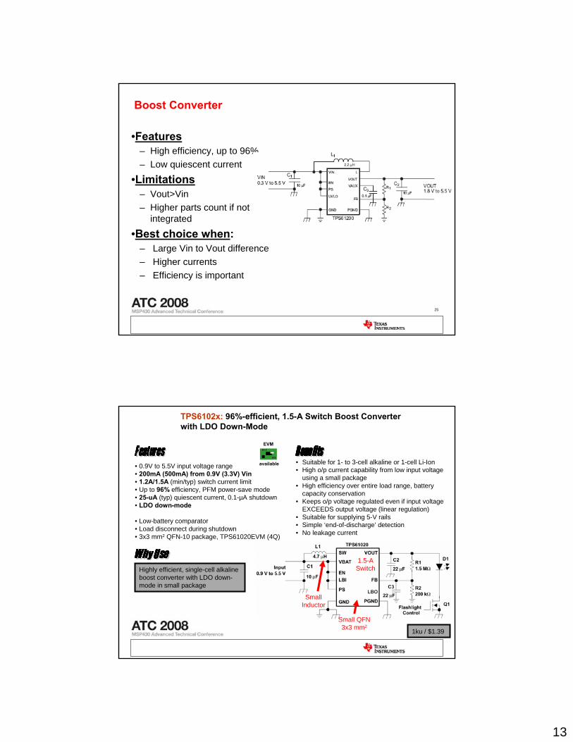
Boost Converter
•Features – High efficiency, up to 96%– Low quiescent current
•Limitations– Vout>Vin– Higher parts count if not
integrated
•Best choice when:– Large Vin to Vout difference – Higher currents – Efficiency is important
26
TPS6102x: 96%-efficient, 1.5-A Switch Boost Converter with LDO Down-Mode
• Suitable for 1- to 3-cell alkaline or 1-cell Li-Ion • High o/p current capability from low input voltage
using a small package• High efficiency over entire load range, battery
capacity conservation• Keeps o/p voltage regulated even if input voltage
EXCEEDS output voltage (linear regulation)• Suitable for supplying 5-V rails• Simple ‘end-of-discharge’ detection• No leakage current
Highly efficient, single-cell alkaline boost converter with LDO down-mode in small package
• 0.9V to 5.5V input voltage range• 200mA (500mA) from 0.9V (3.3V) Vin• 1.2A/1.5A (min/typ) switch current limit• Up to 96% efficiency, PFM power-save mode • 25-uA (typ) quiescent current, 0.1-µA shutdown• LDO down-mode
• Low-battery comparator• Load disconnect during shutdown• 3x3 mm2 QFN-10 package, TPS61020EVM (4Q)
Small QFN 3x3 mm2
SmallInductor
1.5-ASwitch
1ku / $1.39
available
EVM
14
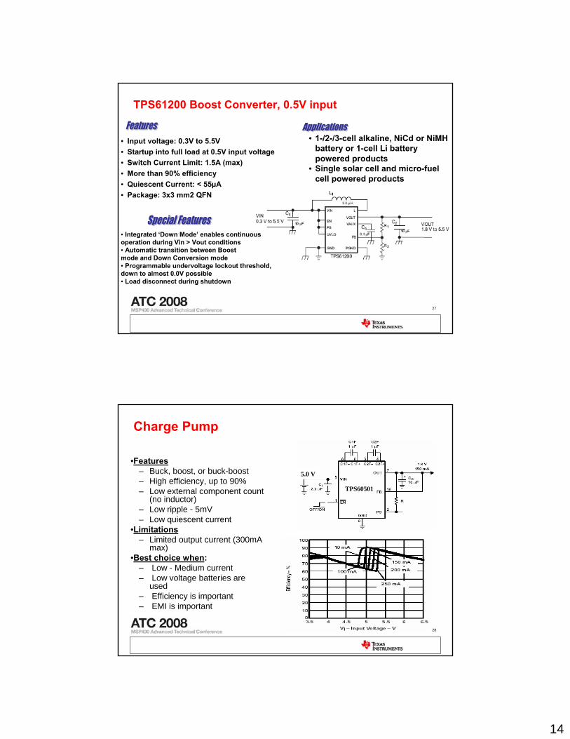
27
• Input voltage: 0.3V to 5.5V• Startup into full load at 0.5V input voltage• Switch Current Limit: 1.5A (max)• More than 90% efficiency• Quiescent Current: < 55µA• Package: 3x3 mm2 QFN
• 1-/2-/3-cell alkaline, NiCd or NiMH battery or 1-cell Li battery powered products
• Single solar cell and micro-fuel cell powered products
• Integrated ‘Down Mode’ enables continuous operation during Vin > Vout conditions• Automatic transition between Boost mode and Down Conversion mode • Programmable undervoltage lockout threshold, down to almost 0.0V possible • Load disconnect during shutdown
TPS61200 Boost Converter, 0.5V input
28
Charge Pump
•Features – Buck, boost, or buck-boost– High efficiency, up to 90%– Low external component count
(no inductor)– Low ripple - 5mV– Low quiescent current
•Limitations– Limited output current (300mA
max)•Best choice when:
– Low - Medium current – Low voltage batteries are
used – Efficiency is important– EMI is important
TPS60501
5.0 V
15
29
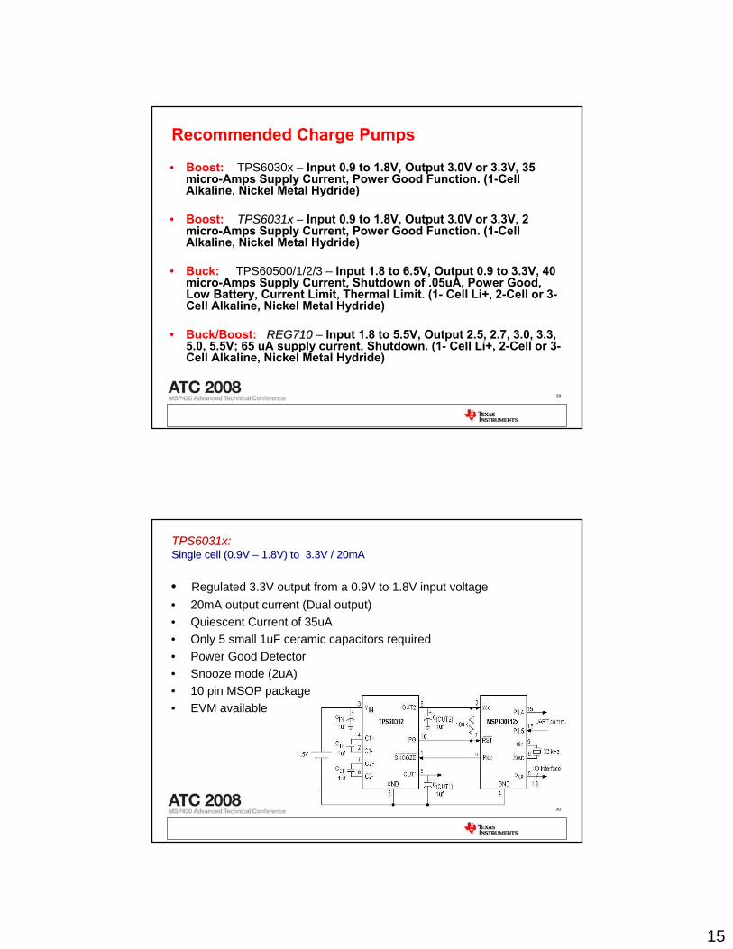
Recommended Charge Pumps
• Boost: TPS6030x – Input 0.9 to 1.8V, Output 3.0V or 3.3V, 35 micro-Amps Supply Current, Power Good Function. (1-Cell Alkaline, Nickel Metal Hydride)
• Boost: TPS6031xTPS6031x – Input 0.9 to 1.8V, Output 3.0V or 3.3V, 2 micro-Amps Supply Current, Power Good Function. (1-Cell Alkaline, Nickel Metal Hydride)
• Buck: TPS60500/1/2/3 – Input 1.8 to 6.5V, Output 0.9 to 3.3V, 40 micro-Amps Supply Current, Shutdown of .05uA, Power Good, Low Battery, Current Limit, Thermal Limit. (1- Cell Li+, 2-Cell or 3-Cell Alkaline, Nickel Metal Hydride)
• Buck/Boost: REG710REG710 – Input 1.8 to 5.5V, Output 2.5, 2.7, 3.0, 3.3, 5.0, 5.5V; 65 uA supply current, Shutdown. (1- Cell Li+, 2-Cell or 3-Cell Alkaline, Nickel Metal Hydride)
30
TPS6031x:TPS6031x:Single cell (0.9V Single cell (0.9V –– 1.8V) to 3.3V / 20mA1.8V) to 3.3V / 20mA
• Regulated 3.3V output from a 0.9V to 1.8V input voltage • 20mA output current (Dual output)• Quiescent Current of 35uA• Only 5 small 1uF ceramic capacitors required• Power Good Detector• Snooze mode (2uA) • 10 pin MSOP package• EVM available
16
31
TPS60310 TPS60310 –– Using with MSP430Using with MSP430
PG sources up to 5mA
32
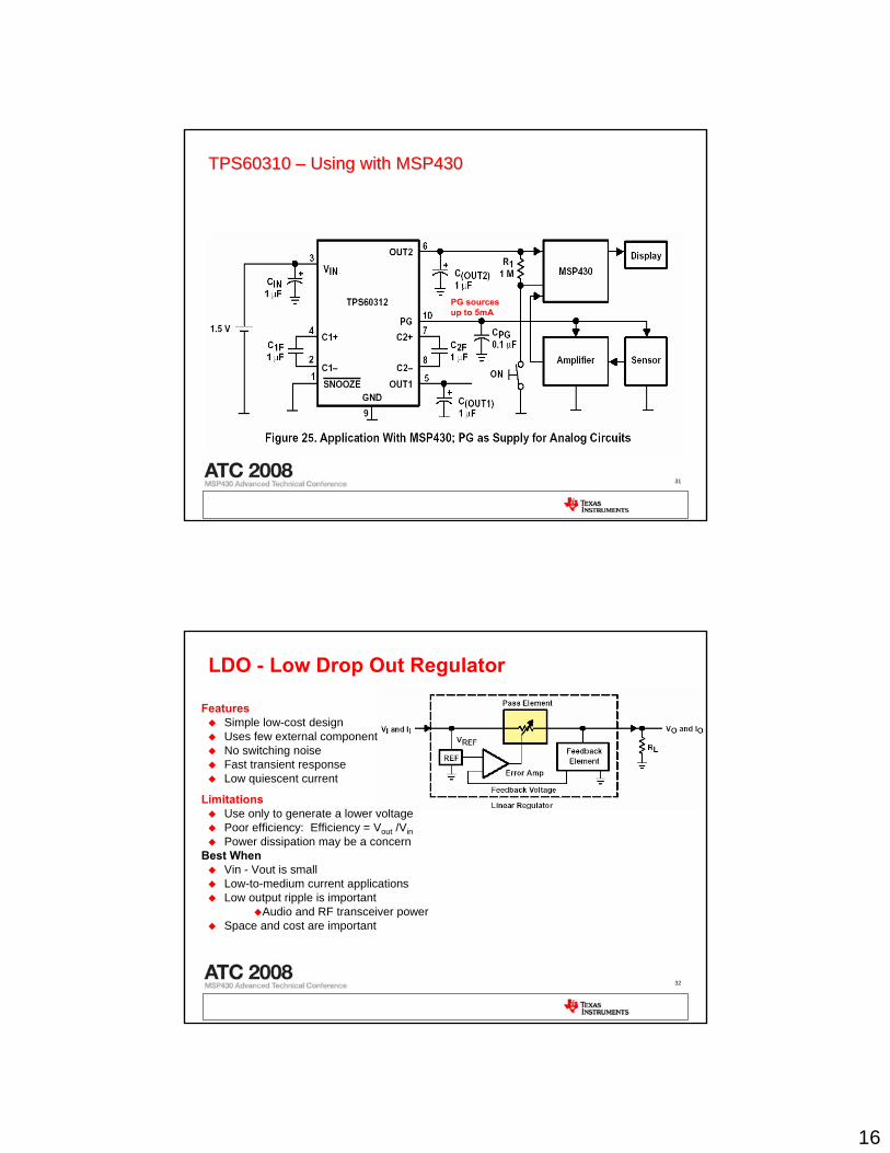
LDO - Low Drop Out Regulator
FeaturesSimple low-cost designUses few external componentsNo switching noiseFast transient responseLow quiescent current
LimitationsUse only to generate a lower voltagePoor efficiency: Efficiency = Vout /VinPower dissipation may be a concern
Best WhenVin - Vout is smallLow-to-medium current applicationsLow output ripple is important
Audio and RF transceiver powerSpace and cost are important
17
33
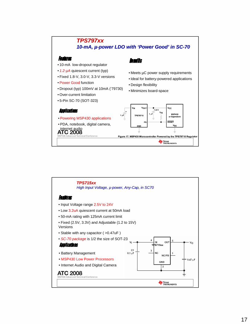
• Meets µC power supply requirements• Ideal for battery-powered applications• Design flexibility• Minimizes board-space
• 10-mA low-dropout regulator• 1.2-µA quiescent current (typ)• Fixed 1.8-V, 3.0-V, 3.3-V versions• Power Good function• Dropout (typ) 100mV at 10mA (‘79730)• Over-current limitation• 5-Pin SC-70 (SOT-323)
• Powering MSP430 applications• PDA, notebook, digital camera, internet audio
TPS797xxTPS797xx1010--mA, mA, µµ--power LDO with power LDO with ‘‘Power GoodPower Good’’ in SCin SC--7070
34
• Input Voltage range 2.5V to 24V• Low 3.2uA quiescent current at 50mA load• 50-mA rating with 125mA current limit• Fixed (2.5V, 3.3V) and Adjustable (1.2 to 15V) Versions• Stable with any capacitor ( >0.47uF ) • SC-70 package is 1/2 the size of SOT-23
TPS715xxTPS715xxHigh Input Voltage, High Input Voltage, µµ--power, Anypower, Any--Cap, in SC70Cap, in SC70
• Battery Management • MSP430 Low Power Processors• Internet Audio and Digital Camera
TPS715xx
18
35
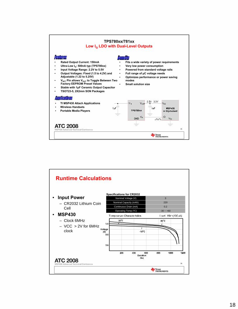
• Rated Output Current: 150mA• Ultra-Low IQ: 500nA typ (TPS780xx)• Input Voltage Range: 2.2V to 5.5V• Output Voltages: Fixed (1.5 to 4.2V) and
Adjustable (1.22 to 5.25V)• VSET Pin allows VOUT to Toggle Between Two
Factory EEPROM Preset Values• Stable with 1μF Ceramic Output Capacitor• TSOT23-5, 2X2mm SON Packages
• TI MSP430 Attach Applications• Wireless Handsets• Portable Media Players
TPS780xx/781xxLow IQ LDO with Dual-Level Outputs
• Fits a wide variety of power requirements• Very low power consumption• Powered from standard voltage rails• Full range of µC voltage needs• Optimizes performance or power saving
modes • Small solution size
36
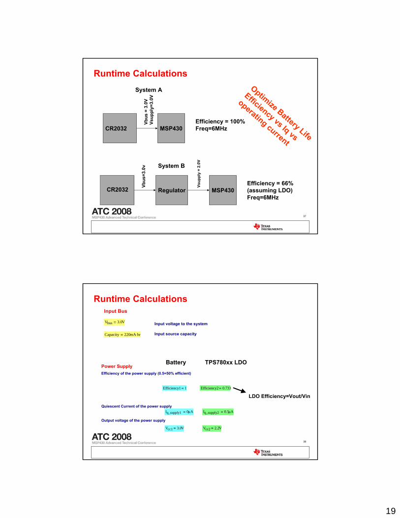
Runtime Calculations
• Input Power– CR2032 Lithium Coin
Cell
• MSP430– Clock 6MHz– VCC > 2V for 6MHz
clock
-30 ~ +60Operating Temp (oC)
0.2Continuous Drain (mA)
220Nominal Capacity (mAh)
3Nominal Voltage (V)Specifications for CR2032
19
37
Runtime CalculationsSystem A
System B
CR2032 MSP430
MSP430Regulator
Vbus
=3.0
v
Vsup
ply
= 2.
0V
Vbus
= 3.
0VVs
uppl
y=3.
0V
Optimize Battery Life
Efficiency vs Iq vs
operating current
Efficiency = 100%Freq=6MHz
Efficiency = 66% (assuming LDO)Freq=6MHz
CR2032
38
Runtime CalculationsInput Bus
Vbus 3.0V≡ Input voltage to the system
Capacity 220mA hr⋅≡ Input source capacity
Power SupplyEfficiency of the power supply (0.5=50% efficient)
Efficiency1 1≡ Efficiency2 0.733≡
Quiescent Current of the power supplyIq_supply1 0μA≡ Iq_supply2 0.5μA≡
Output voltage of the power supply
Vcc1 3.0V≡ Vcc2 2.2V≡
TPS780xx LDO
LDO Efficiency=Vout/Vin
Battery
20
39
Runtime Calculations
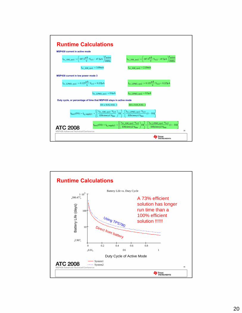
Duty cycle, or percentage of time that MSP430 stays in active mode
D1 0.01 0.02, 1..≡ D2 0.01 0.02, 1..≡
Ibus1 D1( ) Iq_supply1Icc_AM_sys1 Vcc1⋅
Efficiency1 Vbus⋅
⎛⎜⎝
⎞⎟⎠
D1⋅⎡⎢⎣
⎤⎥⎦
+Icc_LPM3_sys1 Vcc1⋅
Efficiency1 Vbus⋅1 D1−( )⋅
⎡⎢⎣
⎤⎥⎦
+:=
Ibus2 D2( ) Iq_supply2Icc_AM_sys2 Vcc2⋅
Efficiency2 Vbus⋅
⎛⎜⎝
⎞⎟⎠
D2⋅⎡⎢⎣
⎤⎥⎦
+Icc_LPM3_sys1 Vcc2⋅
Efficiency2 Vbus⋅1 D2−( )⋅
⎡⎢⎣
⎤⎥⎦
+:=
MSP430 current in active mode
Icc_AM_sys1 187.5μAV
Vcc1⋅ 47.5μA−⎛⎜⎝
⎞⎟⎠
Factive
1MHz:= Icc_AM_sys2 187.5
μAV
Vcc2⋅ 47.5μA−⎛⎜⎝
⎞⎟⎠
Factive
1MHz:=
Icc_AM_sys1 3.09mA= Icc_AM_sys2 2.19mA=
MSP430 current in low power mode 3
Icc_LPM3_sys1 0.125μAV
Vcc1⋅ 0.225μA+:= Icc_LPM3_sys2 0.125μAV
Vcc2⋅ 0.225μA+:=
Icc_LPM3_sys1 0.6μA= Icc_LPM3_sys2 0.5μA=
40
Runtime Calculations
0 0.2 0.4 0.6 0.8
10
100
1 .103
System1System2
Battery Life vs. Duty Cycle
Duty Cycle
Bat
tery
Life
(day
s)
398.477
2.967
Runtime system1 D1( )
3600 24⋅
Runtime system2 D1( )
3600 24⋅
10.01 D1
A 73% efficient solution has longer run time than a 100% efficient solution !!!!!!
Bat
tery
Life
(day
s)
Duty Cycle of Active Mode
Direct from battery
Using TPS780
21
41
Iq is critical in low duty cycle applications
Use same exampleAssume you are aware of TI’s TPS780xx with 0.5uA quiescent currentAssume your competitor uses a std LDO with 20uA of quiescent current
4.16 days14.6 days113 days345 days434 days
0.5uA2190uA20uA0.7333Std LDO
0.48%4.18 daysActive Mode 3600 sec/hour3.4%15.1 daysActive Mode 1000 sec/hour31%148 daysActive Mode 100 sec/hour275%1297 daysActive Mode 10 sec/hour1214%5704 daysActive Mode 1 sec/hour
0.5uAMSP430 Low Power current2190uAMSP430 Active current0.5uAIq0.7333Efficiency
% increaseTPS780
42
Iq is critical in low duty cycle applications
0 0.02 0.04 0.06 0.08
10
100
1 .103
1 .104
System1System2
Battery Life vs. Duty Cycle
Duty Cycle
Bat
tery
Life
(day
s)
7.518 103×
4.146
Runtime system1 D1( )
3600 24⋅
Runtime system2 D1( )
3600 24⋅
.11 10 4−× D1
Bat
tery
Life
(day
s)
Duty Cycle of Active Mode
Using TPS780 with 0.5uA IqUsing std LDO with 20uA Iq
22
43
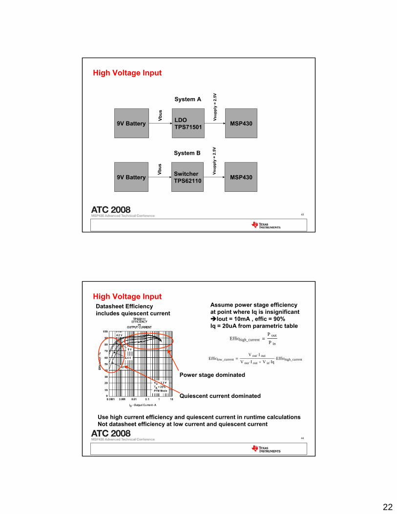
High Voltage Input
System A
MSP430LDOTPS71501
Vbus
Vsup
ply
= 2.
5V
System B
9V Battery MSP430SwitcherTPS62110
Vbus
Vsup
ply
= 2.
5V
9V Battery
44
High Voltage InputDatasheet Efficiency includes quiescent current
Assume power stage efficiency at point where Iq is insignificant
Iout = 10mA , effic = 90%Iq = 20uA from parametric table
Effichigh_currentP out
P in≡
Efficlow_currentV out I out⋅
V out I out⋅ V in Iq⋅+Effichigh_current⋅≡
Power stage dominated
Quiescent current dominated
Use high current efficiency and quiescent current in runtime calculationsNot datasheet efficiency at low current and quiescent current
23
45
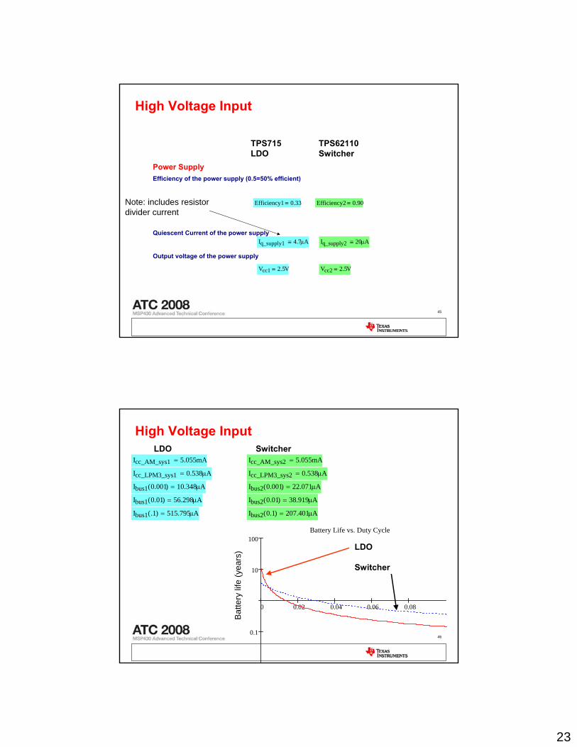
High Voltage Input
Power SupplyEfficiency of the power supply (0.5=50% efficient)
Efficiency1 0.33≡ Efficiency2 0.90≡
Quiescent Current of the power supplyIq_supply1 4.7μA≡ Iq_supply2 20μA≡
Output voltage of the power supply
Vcc1 2.5V≡ Vcc2 2.5V≡
TPS715 TPS62110LDO Switcher
Note: includes resistordivider current
46
0 0.02 0.04 0.06 0.08
0.1
10
100Battery Life vs. Duty Cycle
High Voltage Input
LDO
Switcher
LDO Switcher
Bat
tery
life
(yea
rs)
Icc_AM_sys1 5.055mA= Icc_AM_sys2 5.055mA=
Icc_LPM3_sys1 0.538μA= Icc_LPM3_sys2 0.538μA=
Ibus1 0.001( ) 10.348μA= Ibus2 0.001( ) 22.071μA=
Ibus1 0.01( ) 56.298μA= Ibus2 0.01( ) 38.919μA=
Ibus1 .1( ) 515.795μA= Ibus2 0.1( ) 207.401μA=
24
47
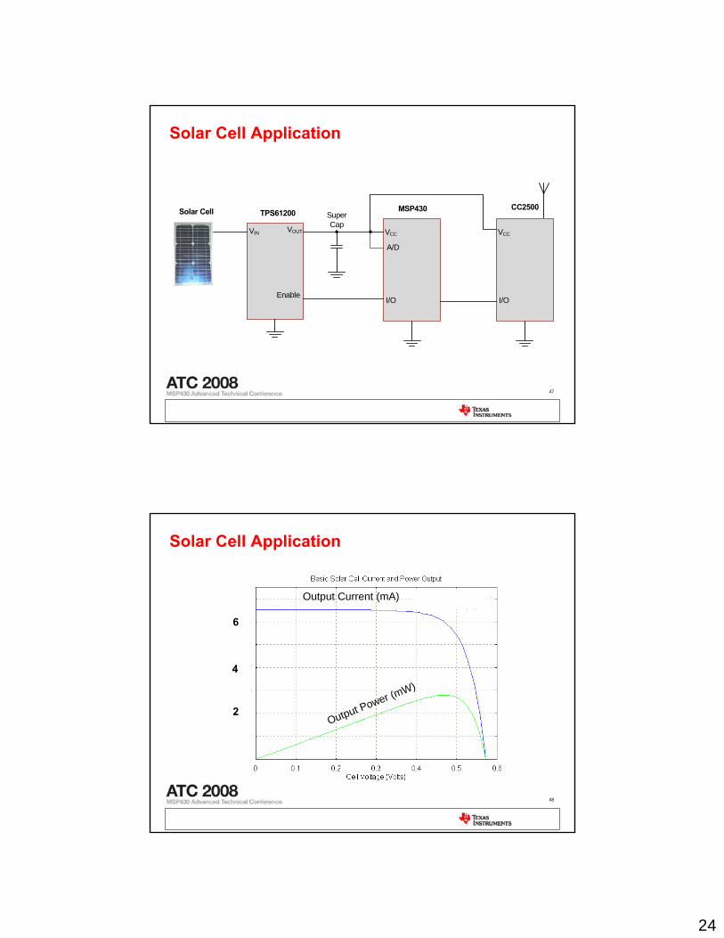
Solar Cell Application
VCC
I/O
MSP430
VIN VOUT
TPS61200
VCC
I/O
CC2500
Enable
Super Cap
A/D
Solar Cell
48
Solar Cell Application
2
4
6
Output Power (mW)
Output Current (mA)
25
49
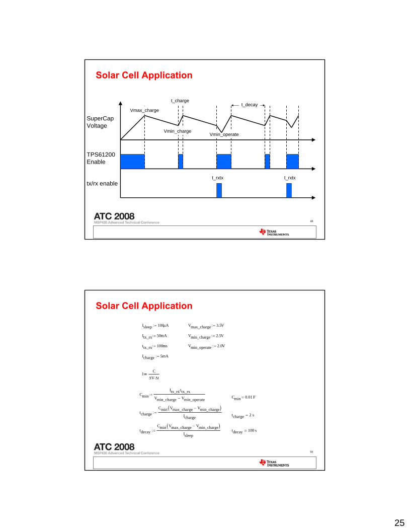
Solar Cell Application
tx/rx enable
TPS61200Enable
SuperCapVoltage
Vmax_charge
Vmin_chargeVmin_operate
t_charget_decay
t_rxtx t_rxtx
50
Solar Cell Application
Isleep 100μA:= Vmax_charge 3.5V:=
Itx_rx 50mA:= Vmin_charge 2.5V:=
ttx_rx 100ms:= Vmin_operate 2.0V:=
Icharge 5mA:=
IC
ΔV Δt⋅
CminItx_rx ttx_rx⋅
Vmin_charge Vmin_operate−:= Cmin 0.01 F=
tchargeCmin Vmax_charge Vmin_charge−( )⋅
Icharge:= tcharge 2 s=
tdecayCmin Vmax_charge Vmin_charge−( )⋅
Isleep:= tdecay 100 s=
26
51
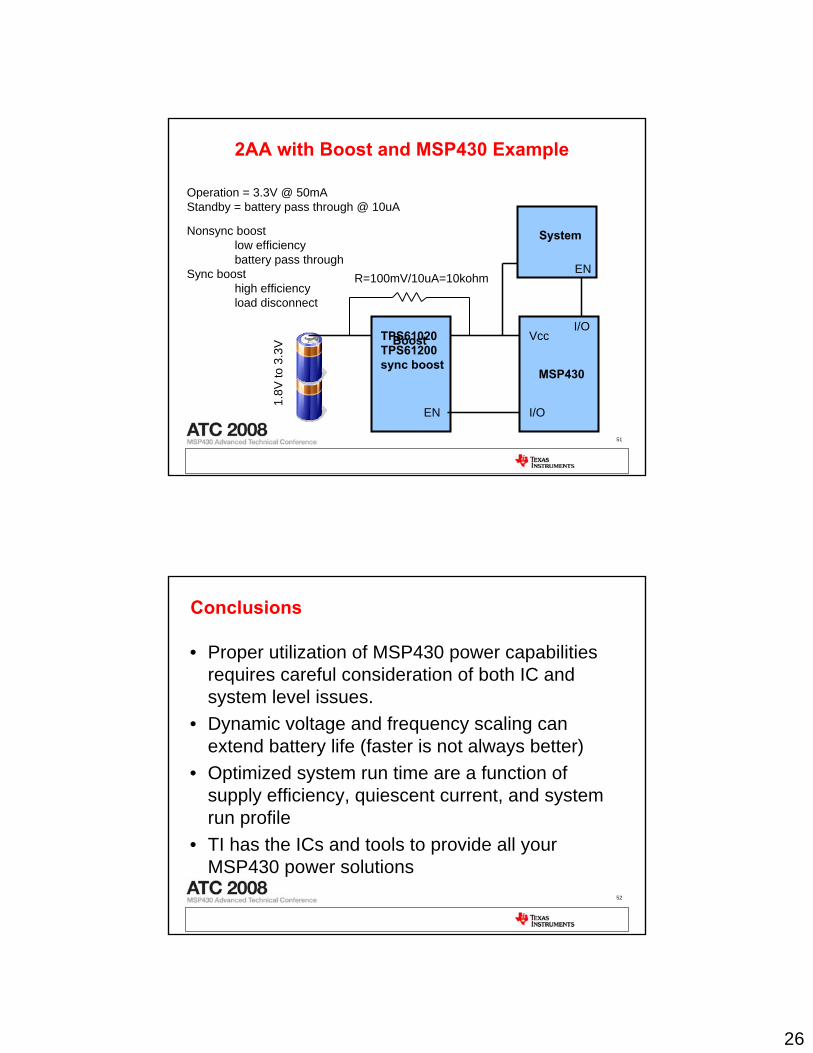
2AA with Boost and MSP430 Example
EN
MSP430
TPS61020TPS61200 sync boost
I/O
I/O
EN
Vcc
System
1.8V
to 3
.3V Boost
Operation = 3.3V @ 50mAStandby = battery pass through @ 10uA
Nonsync boostlow efficiencybattery pass through
Sync boost high efficiencyload disconnect
R=100mV/10uA=10kohm
52
Conclusions
• Proper utilization of MSP430 power capabilities requires careful consideration of both IC and system level issues.
• Dynamic voltage and frequency scaling can extend battery life (faster is not always better)
• Optimized system run time are a function of supply efficiency, quiescent current, and system run profile
• TI has the ICs and tools to provide all your MSP430 power solutions