msi logic circuits
TRANSCRIPT
CHAPTER -9
MSI LOGIC CIRCUITS
Instructor: Afroza Sultana
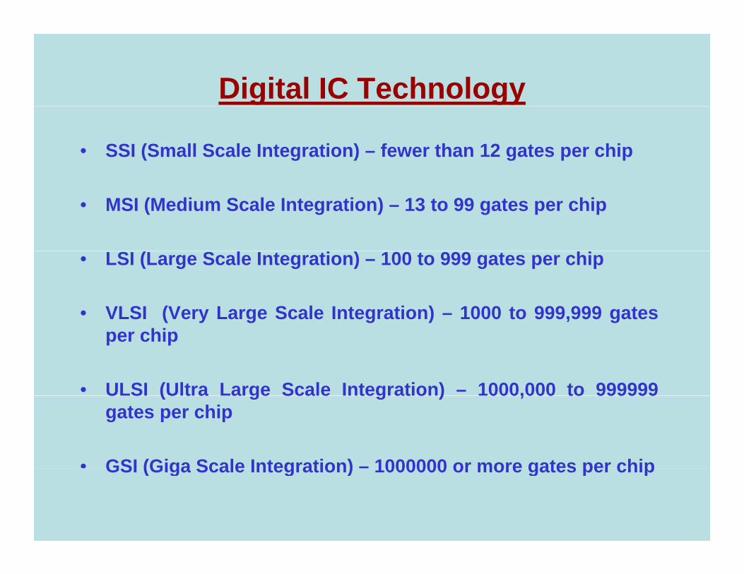
Digital IC Technology
• SSI (Small Scale Integration) – fewer than 12 gates per chip
• MSI (Medium Scale Integration) – 13 to 99 gates per chip
• LSI (Large Scale Integration) – 100 to 999 gates per chip
• VLSI (Very Large Scale Integration) – 1000 to 999,999 gatesper chip
• ULSI (Ultra Large Scale Integration) – 1000,000 to 999999U S (U t a a ge Sca e teg at o ) 000,000 to 999999gates per chip
• GSI (Giga Scale Integration) – 1000000 or more gates per chipGSI (Giga Scale Integration) – 1000000 or more gates per chip

The evolution of IC technique
Tran Single SSI MSI LSI VLSI ULSI GSI1947 1950 1961 1966 1971 1980 1985 1990
sistor component
100 1000 20000LogicGate count
---- ---- 10100~
1000
1000~
20000
20000~
500,000
>500,000
>10,000,000
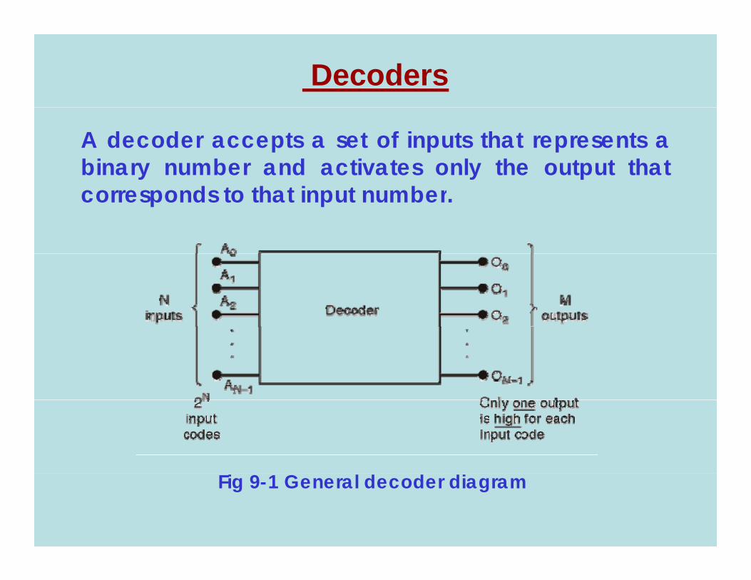
Decoders
A decoder accepts a set of inputs that represents abinary number and activates only the output thatcorresponds to that input number.
Fig 9-1 General decoder diagram

3-line-to-8-line (or 1-of-8) decoder

3-line-to-8-line (or 1-of-8) decoder
Some decoders haveone or more ENABLEinputs used to controlthe operation of thedecoderdecoder.
Fig 9-3 (a) Logic diagram for
74ALS138 decoder(b) truth table(c) logic symbol
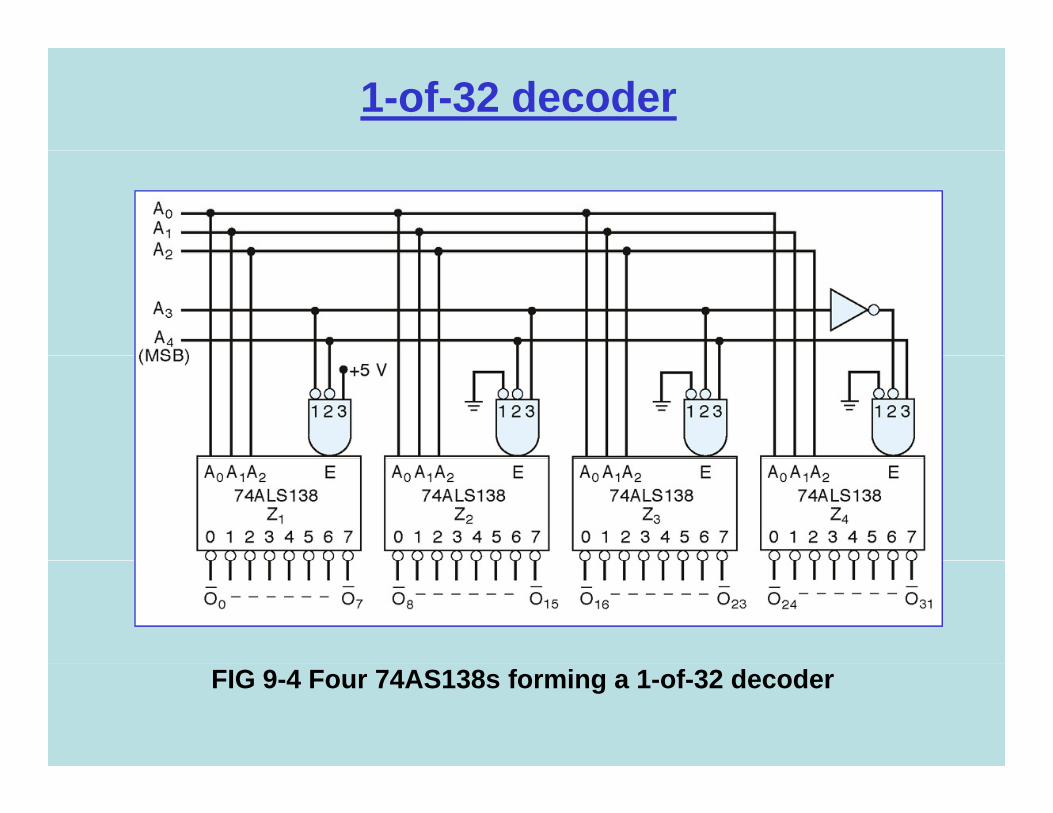
1-of-32 decoder
FIG 9-4 Four 74AS138s forming a 1-of-32 decoder
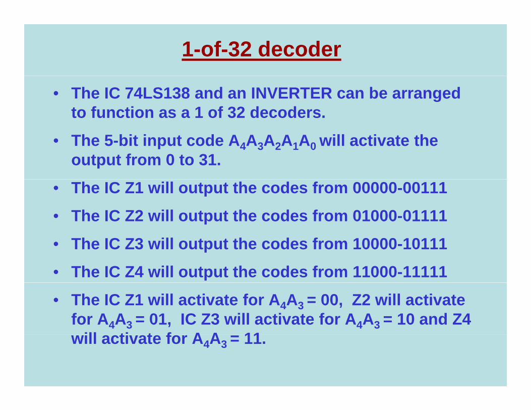
1-of-32 decoder
• The IC 74LS138 and an INVERTER can be arranged to function as a 1 of 32 decoders.
• The 5-bit input code A4A3A2A1A0 will activate the output from 0 to 31.
• The IC Z1 will output the codes from 00000-00111• The IC Z2 will output the codes from 01000-01111• The IC Z3 will output the codes from 10000-10111• The IC Z4 will output the codes from 11000-11111• The IC Z1 will activate for A4A3 = 00, Z2 will activate
for A4A3 = 01, IC Z3 will activate for A4A3 = 10 and Z4 ill ti t f A A 11will activate for A4A3 = 11.

BCD-to-decimal decoder
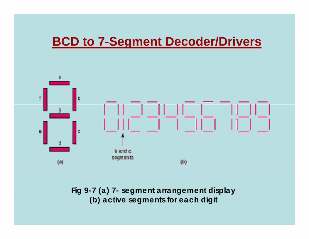
BCD to 7-Segment Decoder/DriversBCD to 7 Segment Decoder/Drivers
Fig 9-7 (a) 7- segment arrangement display (b) active segments for each digit

BCD to 7-Segment Decoder/Drivers
BCD-to-7-segment decoder/driver driving a 7-segment LEDdisplay

Encoder
The opposite of decoding process is called encodingand it is performed by a logic circuit called encoder.Di it l i it th t d t t dDigital circuit that produces an output codedepending on which of its inputs is activated.
Fig 9-12 General encoder diagram.

Octal-to-binary (8-line-to-3-line) Encoder
Fig 9-13 Logic circuit for an octal-to-binary (8-line-to-3-line) encoder For proper operation only one input should be encoder. For proper operation, only one input should be
active at one time.
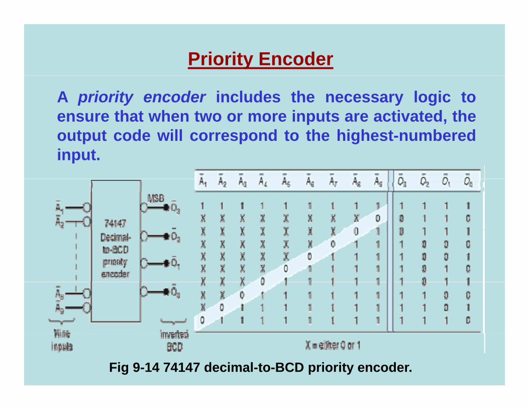
Priority Encoder
A priority encoder includes the necessary logic toensure that when two or more inputs are activated, theoutput code will correspond to the highest-numberedinput.
Fig 9-14 74147 decimal-to-BCD priority encoder.
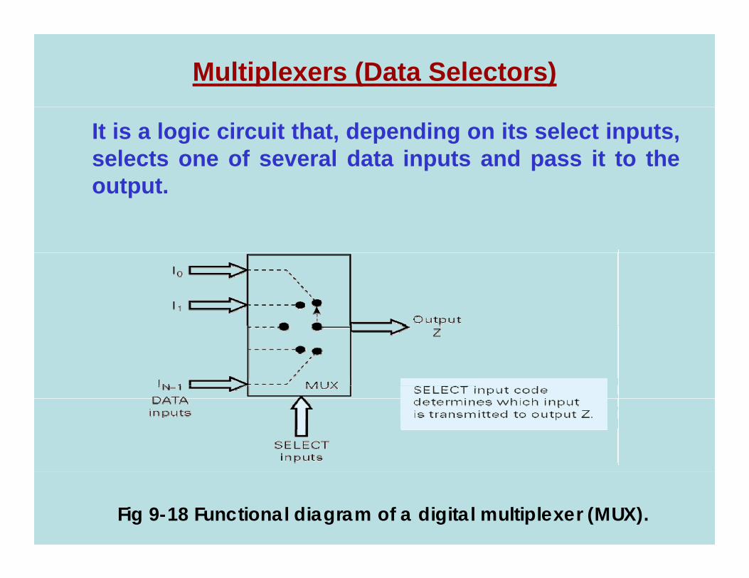
Multiplexers (Data Selectors)
It is a logic circuit that, depending on its select inputs,selects one of several data inputs and pass it to the
t toutput.
Fig 9-18 Functional diagram of a digital multiplexer (MUX).
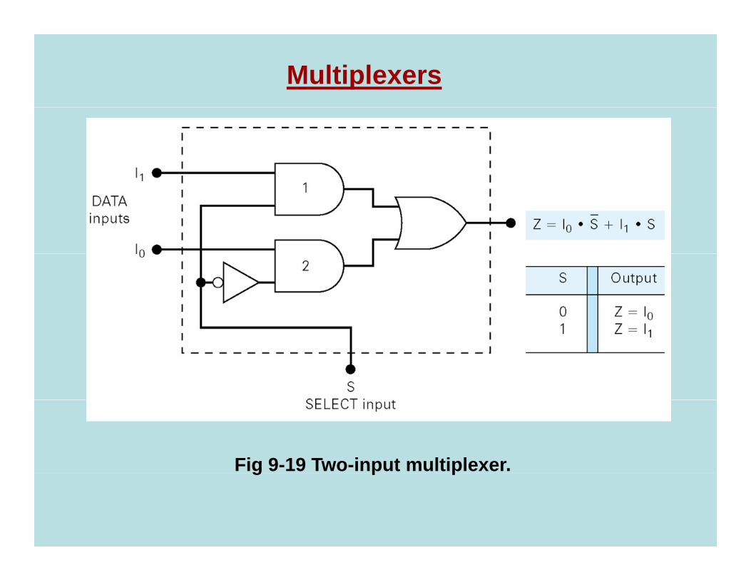
Multiplexers
Fig 9-19 Two-input multiplexer.g p p

MultiplexersMultiplexers
Fig 9-20 Four-input multiplexer.

8- input Multiplexer

16-input Multiplexer
Fig 9-22 Ex. 9-9; two 74HC151s combined to form a 16-input multiplexer.

Multiplexer Applications
D t R tiData Routing: Multiplexers can route data from one of severalsources to one destination. Fig 9-24shows a system fordisplaying two multi digit BCD counters one at a time.

Multiplexer Applications
Parallel-to-Serial Conversion:
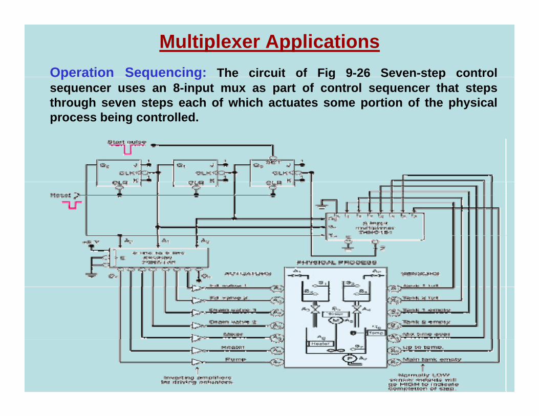
Multiplexer ApplicationsOperation Sequencing: The circuit of Fig 9-26 Seven-step controlOpe at o Seque c g e c cu t o g 9 6 Se e step co t osequencer uses an 8-input mux as part of control sequencer that stepsthrough seven steps each of which actuates some portion of the physicalprocess being controlled.

Multiplexer Applications
Logic Function Generation:Fig 9-27 Mux used to implement a logic function
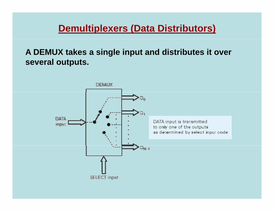
Demultiplexers (Data Distributors)
A DEMUX takes a single input and distributes it over several outputs.p
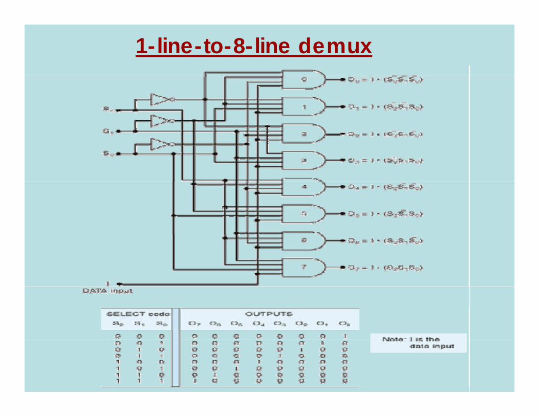
1-line-to-8-line demux

De-Multiplexer Applications
• Clock Demultiplexer: Under control of the SELECT
p pp
Clock Demultiplexer: Under control of the SELECTinputs the clock signal is routed to the desireddestination (fig-9-31).S S /• Security Monitoring System: The open/close statusof an industrial plant is monitored and displayed byLEDs on a remote monitoring panel at the securityg p ystation (fig:9-32).
• Synchronous Data Transmission System: Used toi ll t it f 4 bit d t d fserially transmit four 4-bit data words from a
transmitter to a remote receiver (fig:9-33).
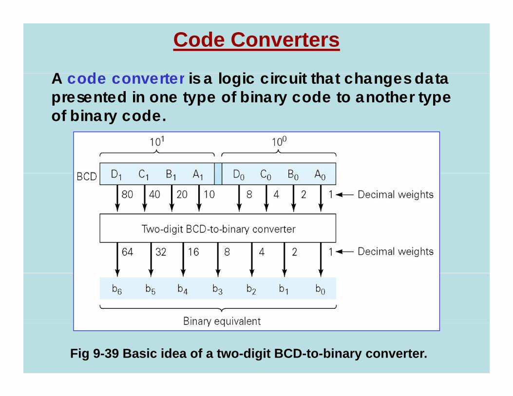
Code Converters
A d t i l i i it th t h d t A code converter is a logic circuit that changes data presented in one type of binary code to another type of binary code. y
Fig 9-39 Basic idea of a two-digit BCD-to-binary converter.

BCD-to-Binary Conversion
• Compute the binary sum of the binary equivalents of all bits in the BCD representation that are 1s.
Example 0101 0010(BCD)0101 0010(BCD)
= 0000010 (2) + 0001010 (10) + 0101000 (40)= 0110100 (52) ( )
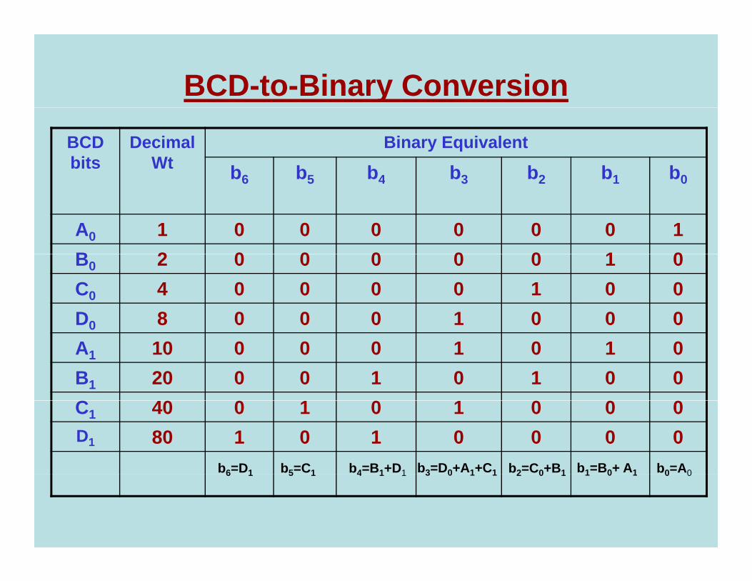
BCD-to-Binary ConversionBCD bits
Decimal Wt
Binary Equivalent
b6 b5 b4 b3 b2 b1 b06 5 4 3 2 1 0
A0 1 0 0 0 0 0 0 1B 2 0 0 0 0 0 1 0B0 2 0 0 0 0 0 1 0C0 4 0 0 0 0 1 0 0D0 8 0 0 0 1 0 0 00
A1 10 0 0 0 1 0 1 0B1 20 0 0 1 0 1 0 0C 40 0 1 0 1 0 0 0C1 40 0 1 0 1 0 0 0D1 80 1 0 1 0 0 0 0
b6=D1 b5=C1 b4=B1+D1 b3=D0+A1+C1 b2=C0+B1 b1=B0+ A1 b0=A06 1 5 1 4 1 1 3 0 1 1 2 0 1 1 0 1 0 0
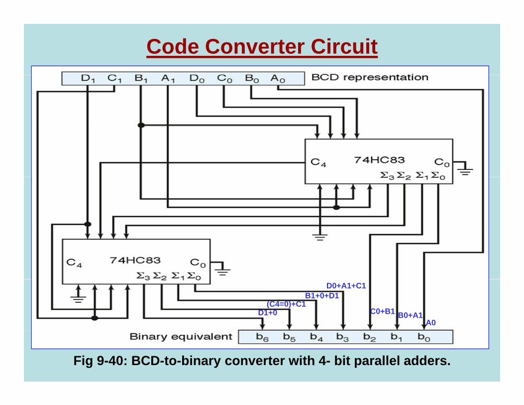
Code Converter Circuit
A0B0+A1C0+B1
D0+A1+C1B1+0+D1
(C4=0)+C1D1+0
Fig 9-40: BCD-to-binary converter with 4- bit parallel adders.