ms210 datasheet v004a - apaltech.comapaltech.com/files/data/ms210/ms210_ datasheet_ v0 4_en.pdf ·...
TRANSCRIPT
MS210
MS210 DS004 www.mshinetek.com - 1 -
The above information is the exclusive intellectual property of M-Shine Technologies Corporation and shall not be disclosed, distributed without permission from M-Shine.
MMMSSS222111000 SSSiiimmmpppllleee SSSPPPIII RRReeecccooorrrdddeeerrr IIICCC
WWWiiittthhh VVVoooiiiccceee CCChhhaaannngggeeerrr DDDaaatttaaassshhheeeeeettt
MMMSSShhhiiinnneee TTTeeeccchhhnnnooolllooogggiiieeesss CCCooorrrpppooorrraaatttiiiooonnn
HEAD QUARTER
Floor 2, No 1008, Chung-Hsing Rd Sec 4,
Chu-Tung, Hsinchu, 31061, Taiwan TEL: +886-3-5833899 FAX: +886-3-5830858
ShenZhen/China Office:
TEL: +86-755-26642629 FAX:+86-755-86210681

MS210
MS210 DS004 www.mshinetek.com - 2 -
The above information is the exclusive intellectual property of M-Shine Technologies Corporation and shall not be disclosed, distributed without permission from M-Shine.
Contents
CONTENTS ....................................................................................................................................................... 2 FIGURES .......................................................................................................................................................... 3 FEATURES........................................................................................................................................................ 4 BLOCK DIAGRAM............................................................................................................................................ 5 APPLICATION .................................................................................................................................................. 5 PACKAGE......................................................................................................................................................... 5 GENERAL DESCRIPTION................................................................................................................................. 5 PAD CONFIGURATION (DRAFT) .................................................................................................................... 6 PINS CONFIGURATION.................................................................................................................................... 7 PIN DESCRIPTIONS.......................................................................................................................................... 7 GENERAL FUNCTIONAL DESCRIPTION........................................................................................................ 11 RESET AND INITIALIZATION ........................................................................................................................ 11
Manual Reset..................................................................................................................................................... 12 USED SPI COMMANDS.................................................................................................................................. 13 RECORDING FUNCTION DESCRIPTION ........................................................................................................ 14
Record Timing................................................................................................................................................... 14 Recording Signal Path....................................................................................................................................... 15 Microphone Amplifier Circuits ......................................................................................................................... 17 SPI Flash Recording Flow ................................................................................................................................ 19 SPI Power Noise Rejection ............................................................................................................................... 20
PLAYING FUNCTION DESCRIPTION ............................................................................................................. 21 Playing Timing Diagram, 1-SEG Mode (SEG2 pin floating) ........................................................................... 21 Playing Timing of 2-SEGMENT Mode ............................................................................................................ 23 RECL over PLAL ............................................................................................................................................. 24 Signal Flow When Playing................................................................................................................................ 25 Playing-Stop Condition..................................................................................................................................... 26 Connecting External Power Amplifier .............................................................................................................. 26 Voice Changer Function.................................................................................................................................... 28
ADPCM CODER AND DECODER (CODEC) ................................................................................................ 30 SAMPLE RATE AND RESISTOR ..................................................................................................................... 30
Double Sample Rate Configuration .................................................................................................................. 30 TYPICAL APPLICATION CIRCUITS............................................................................................................... 31 ABSOLUTE MAXIMUM RATINGS.................................................................................................................. 33 AC & DC ELECTRICAL CHARACTERISTICS ............................................................................................... 33
DC Characteristics ............................................................................................................................................ 33 AC Characteristics ............................................................................................................................................ 34
PACKAGE OUTLINE ...................................................................................................................................... 35

MS210
MS210 DS004 www.mshinetek.com - 3 -
The above information is the exclusive intellectual property of M-Shine Technologies Corporation and shall not be disclosed, distributed without permission from M-Shine.
Figures Figure 1. MS210 Block Diagram....................................................................................................... 5 Figure 2. MS210 PAD Configuration ................................................................................................ 6 Figure 3. MS210 SSOP28 Package configuration............................................................................. 7 Figure 4. VDD Rise Time ................................................................................................................ 12 Figure 5. Manual Reset. ................................................................................................................... 13 Figure 6. Record Timing Diagram. .................................................................................................. 14 Figure 7. MS210 Recording data path. ............................................................................................ 15 Figure 8. MS210 Decimation Filter. ................................................................................................ 15 Figure 9. Decimation Filter Response with 8 KHz sample rate. ..................................................... 16 Figure 10. Decimator Filter Response with 8 KHz sample rate. ..................................................... 17 Figure 11. MS210 Amplifier Components....................................................................................... 17 Figure 12. Operations when recording starts. .................................................................................. 19 Figure 13. Power Noise Rejection Figure........................................................................................ 20 Figure 14. Playing Timing Diagram. ............................................................................................... 22 Figure 15. Playing 2-segment Mode. (Low address first) ............................................................... 23 Figure 16. Playing 2-segment Mode. (High address first)............................................................... 24 Figure 17. RECL interrupt PLAL function. ..................................................................................... 25 Figure 18. Playing signal flow. ........................................................................................................ 26 Figure 19. MS210 Connecting external amplifier of BTL Mode. ................................................... 27 Figure 20. MS210 with external amplifier up to 1 Watt. ................................................................. 27 Figure 21. MS210 with external amplifier up to 10 Watt or more................................................... 28 Figure 22. Signal Flow for ROBOT Effect...................................................................................... 29 Figure 23. Example waveform of ROBOT Effect. .......................................................................... 29 Figure 24. Example Double Sample Rate Configuration. ............................................................... 30 Figure 25. Typical Application Circuit for Recording Application. ................................................ 31 Figure 26. Typical Application for simple Amplifier. ...................................................................... 31 Figure 27. Typical Application for NO-MIC recording................................................................... 32 Figure 28. MS210 with Auto-Repeat modification.......................................................................... 32
MS210
MS210 DS004 www.mshinetek.com - 4 -
The above information is the exclusive intellectual property of M-Shine Technologies Corporation and shall not be disclosed, distributed without permission from M-Shine.
Features
Recording Microphone input to connected SPI flash memory, very low cost. All data kept when power is OFF. 1 MBIT SPI flash may record 30 seconds of speech with 8 KHz sample rate. Supports up to 64 MBIT, which is about 35 minutes with 8 KHz sample rate. Play the recorded sound directly from the SPI flash memory to 8 ohm speaker. Sample-rate is adjusted by external resistor.1 Play pre-recorded voice before or after the later recorded voice. (PAD Option). Pre-recorded voice will
not be erased. Pre-recorded voice can be played with different sample rate with simple external components. Built-in 1280 bytes of RAM for FIFO while erasing flash memory. Operating from 2.3 ~ 4.5V. Sleep power consumption < 10 uA with flash memory. Key button inputs
PLAY, edge trigger or level- hold to play the recorded sound. REC, edge trigger or level-hold to record the voice. RECL can interrupt PLAL operation, suitable for card applications.
BEEP prompt for recording. Voice-Changer Capability when playing recorded voices:
Robot Pitch shift
Playing/Recording LED Driving Playing 3 Hz LED output. Act as band-limited amplifier if TEST and SPIMISO connect to GND, and PLAE connect to LEDBZ.
1 For recording applications, sample rate is limited by 2560/[Flash sector-erase-time]. Recording sample will missing if
recording-sample rate is greater than 2560/[Flash sector-erase-time]. Pre-record sound segment has no such limit.

MS210
MS210 DS004 www.mshinetek.com - 5 -
The above information is the exclusive intellectual property of M-Shine Technologies Corporation and shall not be disclosed, distributed without permission from M-Shine.
Block Diagram
RC OSC
OSC
O
ADC &Filter
FIFO RAM
MICBias OPA
ADPCMCoder
SPI Interface
ADPCMDecoder
& Voice
Changer
D-TypeAMP
KEY INPUT & Options &LED
SPIC
S
SPIC
K
MO
SI
MIS
O
PLAE
REC
ESP
KP
SPK
N
MBI
AS
MIC
N
VC
H
VAG
VAA
LED
P
LEDP3
BEE
PEN
POR
SEG
2
RE
CL
PLA
L
LED
BZ TE
ST
Figure 1. MS210 Block Diagram.
Application
Sound recording toys, cards, and other applications.
Package
SOP-28 PACKAGED.
General Description MS210 is a recording IC that can be used for all kinds of sound recording applications. It can also be
configured as a simplified band-limited sound amplifier. With different SPI flash memory connected, it can
record sound up to 40 minutes with very good sound quality.
MS210
MS210 DS004 www.mshinetek.com - 6 -
The above information is the exclusive intellectual property of M-Shine Technologies Corporation and shall not be disclosed, distributed without permission from M-Shine.
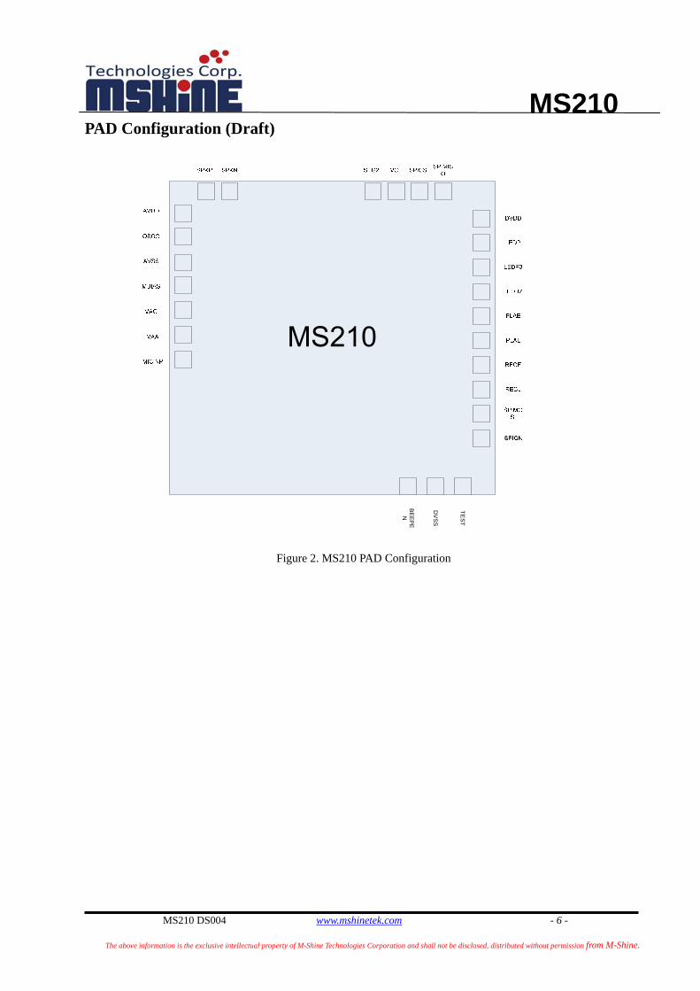
PAD Configuration (Draft)
BEEP
EN
DV
SS
TEST
Figure 2. MS210 PAD Configuration
MS210
MS210 DS004 www.mshinetek.com - 7 -
The above information is the exclusive intellectual property of M-Shine Technologies Corporation and shall not be disclosed, distributed without permission from M-Shine.
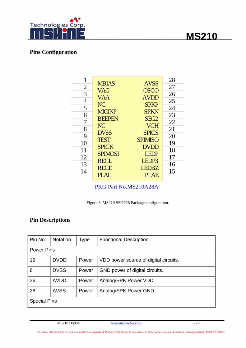
Pins Configuration
MBIAS1
VAG2
VAA3
NC4
MICINP5
BEEPEN6
NC7
DVSS8
TEST9
SPICK10
SPIMOSI11
RECL12
RECE13
PLAL14 PLAE 15LEDBZ 16LEDP3 17LEDP 18DVDD 19SPIMISO 20SPICS 21VCH 22SEG2 23SPKN 24SPKP 25AVDD 26OSCO 27AVSS 28
U2
MS210_SSOP28
Figure 3. MS210 SSOP28 Package configuration.
Pin Descriptions
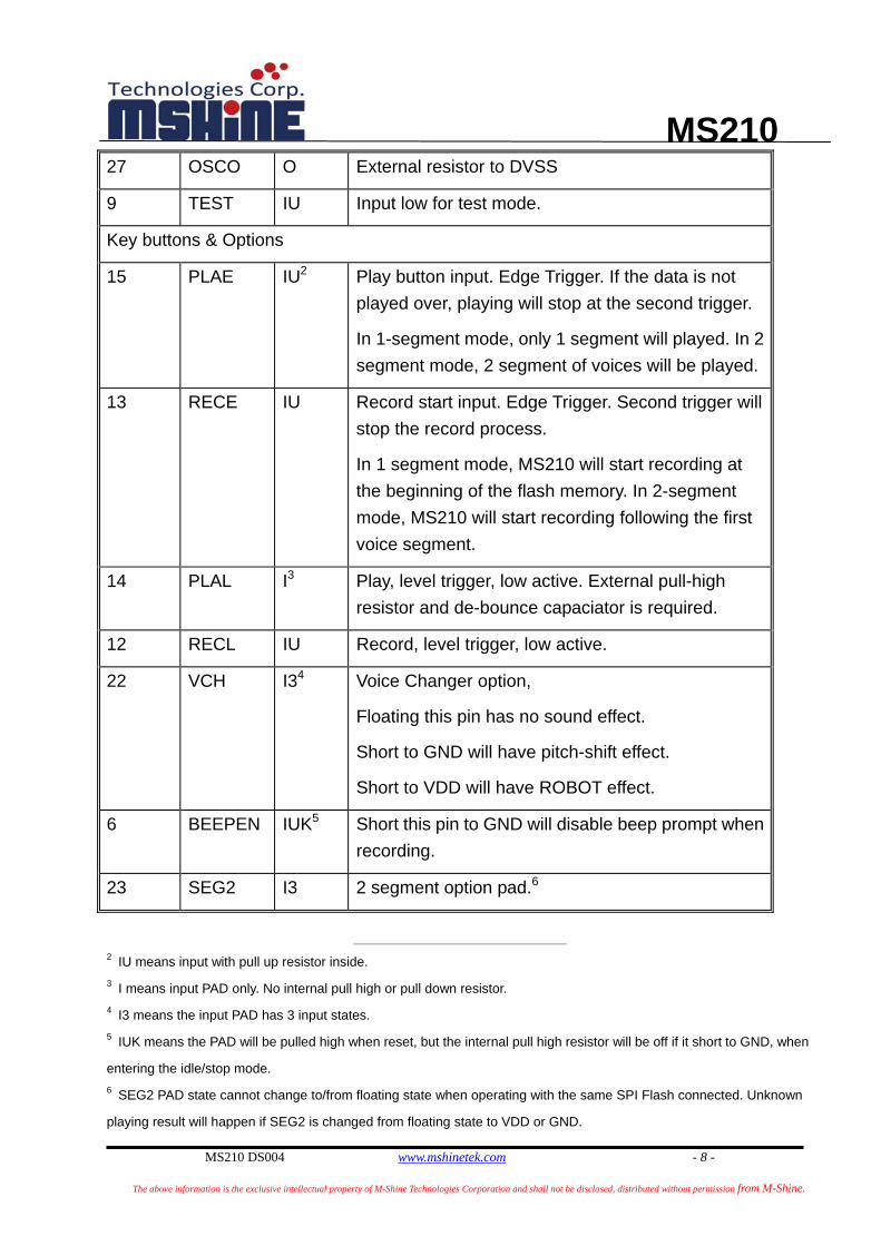
Pin No. Notation Type Functional Description
Power Pins
19 DVDD Power VDD power source of digital circuits.
8 DVSS Power GND power of digital circuits.
26 AVDD Power Analog/SPK Power VDD
28 AVSS Power Analog/SPK Power GND
Special Pins
PKG Part No.MS210A28A
MS210
MS210 DS004 www.mshinetek.com - 8 -
The above information is the exclusive intellectual property of M-Shine Technologies Corporation and shall not be disclosed, distributed without permission from M-Shine.
27 OSCO O External resistor to DVSS
9 TEST IU Input low for test mode.
Key buttons & Options
15 PLAE IU2 Play button input. Edge Trigger. If the data is not played over, playing will stop at the second trigger.
In 1-segment mode, only 1 segment will played. In 2 segment mode, 2 segment of voices will be played.
13 RECE IU Record start input. Edge Trigger. Second trigger will stop the record process.
In 1 segment mode, MS210 will start recording at the beginning of the flash memory. In 2-segment mode, MS210 will start recording following the first voice segment.
14 PLAL I3 Play, level trigger, low active. External pull-high resistor and de-bounce capaciator is required.
12 RECL IU Record, level trigger, low active.
22 VCH I34 Voice Changer option,
Floating this pin has no sound effect.
Short to GND will have pitch-shift effect.
Short to VDD will have ROBOT effect.
6 BEEPEN IUK5 Short this pin to GND will disable beep prompt when recording.
23 SEG2 I3 2 segment option pad.6
2 IU means input with pull up resistor inside. 3 I means input PAD only. No internal pull high or pull down resistor. 4 I3 means the input PAD has 3 input states. 5 IUK means the PAD will be pulled high when reset, but the internal pull high resistor will be off if it short to GND, when
entering the idle/stop mode. 6 SEG2 PAD state cannot change to/from floating state when operating with the same SPI Flash connected. Unknown
playing result will happen if SEG2 is changed from floating state to VDD or GND.
MS210
MS210 DS004 www.mshinetek.com - 9 -
The above information is the exclusive intellectual property of M-Shine Technologies Corporation and shall not be disclosed, distributed without permission from M-Shine.
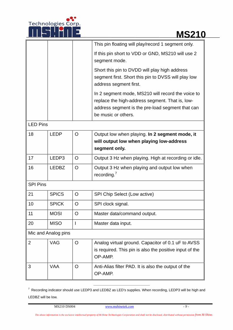
This pin floating will play/record 1 segment only.
If this pin short to VDD or GND, MS210 will use 2 segment mode.
Short this pin to DVDD will play high address segment first. Short this pin to DVSS will play low address segment first.
In 2 segment mode, MS210 will record the voice to replace the high-address segment. That is, low- address segment is the pre-load segment that can be music or others.
LED Pins
18 LEDP O Output low when playing. In 2 segment mode, it will output low when playing low-address segment only.
17 LEDP3 O Output 3 Hz when playing. High at recording or idle.
16 LEDBZ O Output 3 Hz when playing and output low when recording.7
SPI Pins
21 SPICS O SPI Chip Select (Low active)
10 SPICK O SPI clock signal.
11 MOSI O Master data/command output.
20 MISO I Master data input.
Mic and Analog pins
2 VAG O Analog virtual ground. Capacitor of 0.1 uF to AVSS is required. This pin is also the positive input of the OP-AMP.
3 VAA O Anti-Alias filter PAD. It is also the output of the OP-AMP.
7 Recording indicator should use LEDP3 and LEDBZ as LED’s supplies. When recording, LEDP3 will be high and
LEDBZ will be low.

MS210
MS210 DS004 www.mshinetek.com - 10 -
The above information is the exclusive intellectual property of M-Shine Technologies Corporation and shall not be disclosed, distributed without permission from M-Shine.
1 MBIAS O Microphone bias.
5 MICNP I Negative input of internal OP-AMP. A feed back resistor and capacitor is required to connect VAA, and a resistor is used to connect the microphone.
Speaker Driving Pins
25 SPKP O Speaker output. High-Z when not playing.
24 SPKN O Speaker output. High-Z when not playing.
Table 1. MS210 Pins Description.
MS210
MS210 DS004 www.mshinetek.com - 11 -
The above information is the exclusive intellectual property of M-Shine Technologies Corporation and shall not be disclosed, distributed without permission from M-Shine.
General Functional Description MS210 is a simple chip that can record the voice from microphone/Speaker to SPI memory, and play the
voice from SPI memory directly. It built in high-quality ADPCM engine that can compress the voice data from
ADC to 4-bit per sample.
That is, when recording, sound are compressed to 4-bit per sample, and then stored to flash memory. While
erasing sectors on SPI flash memory, MS210 will store the compressed speech data in its own RAM. After
the sector is erased, the compressed data will be written to the SPI memory as soon as possible. Also, it will
overwrite the old record data and replaced by the new one whenever a voice is recorded.
Before start recording a short Beep prompt will be on the speaker. And 2 short “beep” will out after recording
stopped. Beep function can be disabled with BEEPEN short to GND.
In 1-segment mode, MS210 will record the speech from the beginning of the SPI flash. In 2-segment mode,
MS210 will record (overwrite) the speech of high-address voice segment.
When playing, MS210 will read the content from the SPI memory and decode with ADPCM decoder, and
perform the voice-changer function as required. In 1-segment mode, MS210 will play just one voice segment.
In 2-segment mode, MS210 will play 2 segments of voices one by one. Which one should be played first is
defined by PAD option.
MS210 playing is through D-Type Amplifier that has very good power efficiency and sound quality.
If TEST is low and SPIMISO is low, with PLAE connect to LEDBZ, MS210 will be act as band-limited
amplifier like Figure 26.
Reset and Initialization MS210 has default Power-On-Reset (POR) that release at about 1.8 V. After around 300 ms after power-on,
MS210 will start to check the SPI flash memory connected. To power on correctly, the following constrains
must meet:
1. Before Power ON, VDD Must be < 0.3V. (V1 in Figure 4 must less than 3V)
2. After Power ON, VDD must be higher than the voltage that the SPI flash can work (usually 2.4V or 2.7V).
(V2 in Figure 4 must be greater than SPI Flash working voltage).
3. VDD Rise Time must be less than 0.2 second.
4. When power-ON, VDD curve must be monotonic. Bouncing between 0.3V~2.3V is not allowed.

MS210
MS210 DS004 www.mshinetek.com - 12 -
The above information is the exclusive intellectual property of M-Shine Technologies Corporation and shall not be disclosed, distributed without permission from M-Shine.
Time
V1
V2
VDD Rise Time
Figure 4. VDD Rise Time
If SPI Flash does not reply a valid size, MS210 will retry to get the size after a period of time. In 1-segment
mode, MS210 will go to sleep with DS command of the memory after memory size is checked. In 2-segment
mode, MS210 will find the end (sector address) of the first voice segment after reset.
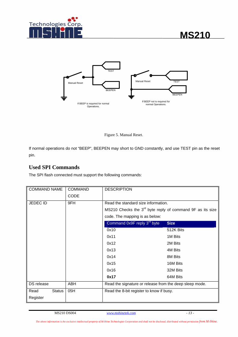
Manual Reset If MS210 is used in bad power conditions, or changing flash memory is required, manual reset is another
option. MS210 will enter “RESET” state if “TEST” and “BEEPEN” short to GND at the same time. The
configurations are as below:
MS210
MS210 DS004 www.mshinetek.com - 13 -
The above information is the exclusive intellectual property of M-Shine Technologies Corporation and shall not be disclosed, distributed without permission from M-Shine.
Manual Reset
TEST
BEEPEN
Manual Reset TEST
BEEPEN
If BEEP is required for normal Operations.
If BEEP not is required for normal Operations.
Figure 5. Manual Reset.
If normal operations do not “BEEP”, BEEPEN may short to GND constantly, and use TEST pin as the reset
pin.
Used SPI Commands The SPI flash connected must support the following commands:
COMMAND NAME COMMAND
CODE
DESCRIPTION
JEDEC ID 9FH Read the standard size information.
MS210 Checks the 3rd byte reply of command 9F as its size
code. The mapping is as below:
Command 0x9F reply 3rd byte Size 0x10 512K Bits
0x11 1M Bits
0x12 2M Bits
0x13 4M Bits
0x14 8M Bits
0x15 16M Bits
0x16 32M Bits
0x17 64M Bits
DS release ABH Read the signature or release from the deep sleep mode.
Read Status
Register
05H Read the 8-bit register to know if busy.
MS210
MS210 DS004 www.mshinetek.com - 14 -
The above information is the exclusive intellectual property of M-Shine Technologies Corporation and shall not be disclosed, distributed without permission from M-Shine.
Write Status
Register
01H Write the 8-bit register.
Write Enable 06H Write enable
Sector Erase 20H Erase 4 Kbyte sector.
Page Program 02H Program 256 bytes.
Deep Power Down B9H Deep power down of the SPI Flash memory.
Data Read 03H Read the SPI flash memory.
Table 2. Used SPI commands.
New SPI Memory parts must have above commands if connecting to MS210.
Recording Function Description MS210 will record the signal of microphone to the SPI Flash Memory, the following sub-sections will describe
the detailed information.
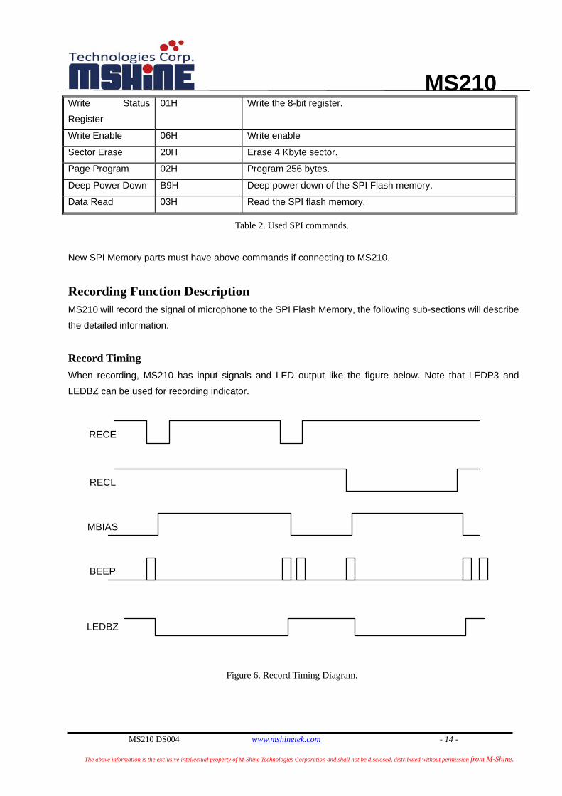
Record Timing When recording, MS210 has input signals and LED output like the figure below. Note that LEDP3 and
LEDBZ can be used for recording indicator.
RECE
RECL
MBIAS
BEEP
LEDBZ
Figure 6. Record Timing Diagram.
MS210
MS210 DS004 www.mshinetek.com - 15 -
The above information is the exclusive intellectual property of M-Shine Technologies Corporation and shall not be disclosed, distributed without permission from M-Shine.
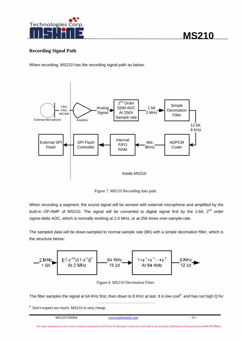
Recording Signal Path
When recording, MS210 has the recording signal path as below.
2nd Order SDM ADCAt 256X
Sample rateAmplifier
VAA,VAG,
MICINP
External Microphone
SimpleDecimation
Filter
AnalogSignal
ADPCMCoder
Internal FIFORAM
SPI Flash Controller
External SPIFlash
1 bit2 MHz
12 bit,8 KHz
Inside MS210
4bit,8KHz
Figure 7. MS210 Recording data path.
When recording a segment, the sound signal will be sensed with external microphone and amplified by the
built-in OP-AMP of MS210. The signal will be converted to digital signal first by the 1-bit, 2nd order
sigma-delta ADC, which is normally working at 2.0 MHz, or at 256 times over-sample-rate.
The sampled data will be down-sampled to normal sample rate (8K) with a simple decimation filter, which is
the structure below:
Figure 8. MS210 Decimation Filter.
The filter samples the signal at 64 KHz first, then down to 8 KHz at last. It is low cost8 and has not high Q for
8 Don’t expect too much, MS210 is very cheap.
MS210
MS210 DS004 www.mshinetek.com - 16 -
The above information is the exclusive intellectual property of M-Shine Technologies Corporation and shall not be disclosed, distributed without permission from M-Shine.
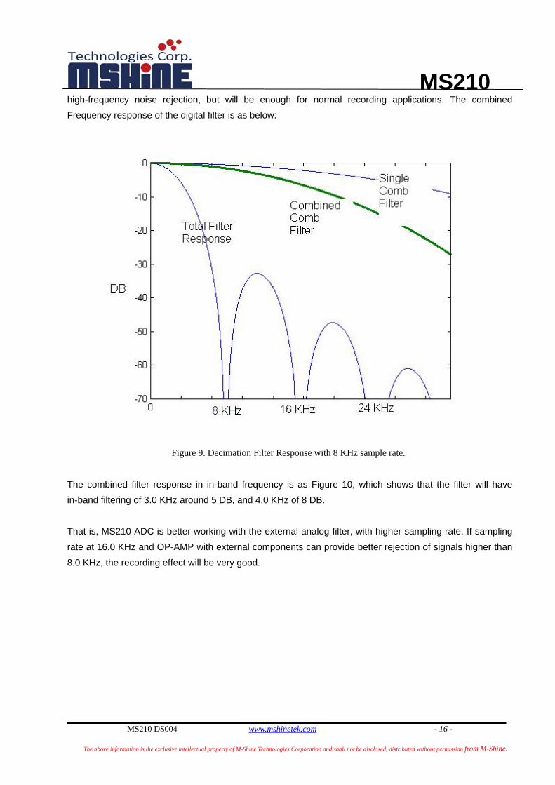
high-frequency noise rejection, but will be enough for normal recording applications. The combined
Frequency response of the digital filter is as below:
Figure 9. Decimation Filter Response with 8 KHz sample rate.
The combined filter response in in-band frequency is as Figure 10, which shows that the filter will have
in-band filtering of 3.0 KHz around 5 DB, and 4.0 KHz of 8 DB.
That is, MS210 ADC is better working with the external analog filter, with higher sampling rate. If sampling
rate at 16.0 KHz and OP-AMP with external components can provide better rejection of signals higher than
8.0 KHz, the recording effect will be very good.

MS210
MS210 DS004 www.mshinetek.com - 17 -
The above information is the exclusive intellectual property of M-Shine Technologies Corporation and shall not be disclosed, distributed without permission from M-Shine.
Figure 10. Decimator Filter Response with 8 KHz sample rate.
Microphone Amplifier Circuits MS210 has an OP-AMP that can amplify the audio signal as required. Usually the external components are
as follows.
Figure 11. MS210 Amplifier Components.
MS210
MS210 DS004 www.mshinetek.com - 18 -
The above information is the exclusive intellectual property of M-Shine Technologies Corporation and shall not be disclosed, distributed without permission from M-Shine.
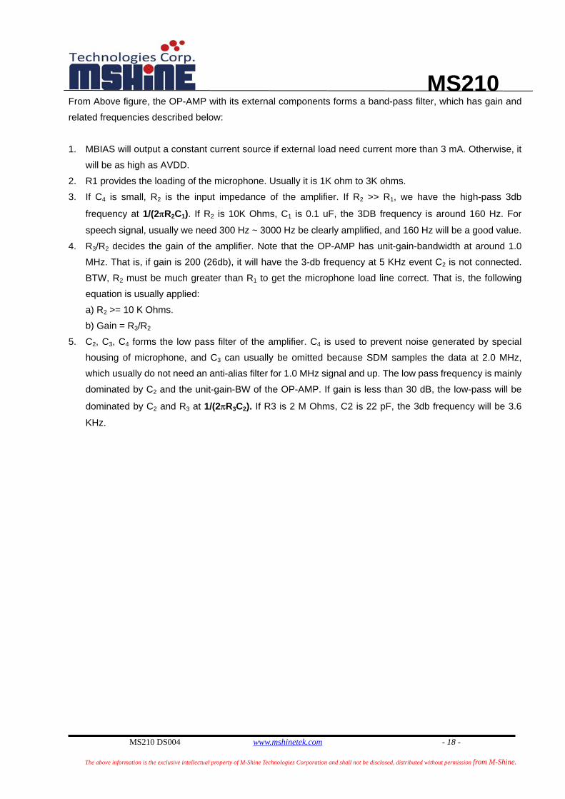
From Above figure, the OP-AMP with its external components forms a band-pass filter, which has gain and
related frequencies described below:
1. MBIAS will output a constant current source if external load need current more than 3 mA. Otherwise, it
will be as high as AVDD.
2. R1 provides the loading of the microphone. Usually it is 1K ohm to 3K ohms.
3. If C4 is small, R2 is the input impedance of the amplifier. If R2 >> R1, we have the high-pass 3db
frequency at 1/(2πR2C1). If R2 is 10K Ohms, C1 is 0.1 uF, the 3DB frequency is around 160 Hz. For
speech signal, usually we need 300 Hz ~ 3000 Hz be clearly amplified, and 160 Hz will be a good value.
4. R3/R2 decides the gain of the amplifier. Note that the OP-AMP has unit-gain-bandwidth at around 1.0
MHz. That is, if gain is 200 (26db), it will have the 3-db frequency at 5 KHz event C2 is not connected.
BTW, R2 must be much greater than R1 to get the microphone load line correct. That is, the following
equation is usually applied:
a) R2 >= 10 K Ohms.
b) Gain = R3/R2
5. C2, C3, C4 forms the low pass filter of the amplifier. C4 is used to prevent noise generated by special
housing of microphone, and C3 can usually be omitted because SDM samples the data at 2.0 MHz,
which usually do not need an anti-alias filter for 1.0 MHz signal and up. The low pass frequency is mainly
dominated by C2 and the unit-gain-BW of the OP-AMP. If gain is less than 30 dB, the low-pass will be
dominated by C2 and R3 at 1/(2πR3C2). If R3 is 2 M Ohms, C2 is 22 pF, the 3db frequency will be 3.6
KHz.
MS210
MS210 DS004 www.mshinetek.com - 19 -
The above information is the exclusive intellectual property of M-Shine Technologies Corporation and shall not be disclosed, distributed without permission from M-Shine.
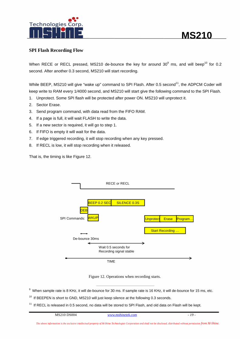
SPI Flash Recording Flow
When RECE or RECL pressed, MS210 de-bounce the key for around 309 ms, and will beep10 for 0.2
second. After another 0.3 second, MS210 will start recording.
While BEEP, MS210 will give “wake up” command to SPI Flash. After 0.5 second11, the ADPCM Coder will
keep write to RAM every 1/4000 second, and MS210 will start give the following command to the SPI Flash.
1. Unprotect. Some SPI flash will be protected after power ON. MS210 will unprotect it.
2. Sector Erase.
3. Send program command, with data read from the FIFO RAM.
4. If a page is full, it will wait FLASH to write the data.
5. If a new sector is required, it will go to step 1.
6. If FIFO is empty it will wait for the data.
7. If edge triggered recording, it will stop recording when any key pressed.
8. If RECL is low, it will stop recording when it released.
That is, the timing is like Figure 12.
DEB
BEEP 0.2 SEC SILENCE 0.3S
WKUPSPI Commands:
RECE or RECL
Unprotect Erase
Start Recording …
Program…
De-bounce 30ms
Wait 0.5 seconds for Recording signal stable
TIME
Figure 12. Operations when recording starts.
9 When sample rate is 8 KHz, it will de-bounce for 30 ms. If sample rate is 16 KHz, it will de-bounce for 15 ms, etc. 10 If BEEPEN is short to GND, MS210 will just keep silence at the following 0.3 seconds. 11 If RECL is released in 0.5 second, no data will be stored to SPI Flash, and old data on Flash will be kept.
MS210
MS210 DS004 www.mshinetek.com - 20 -
The above information is the exclusive intellectual property of M-Shine Technologies Corporation and shall not be disclosed, distributed without permission from M-Shine.
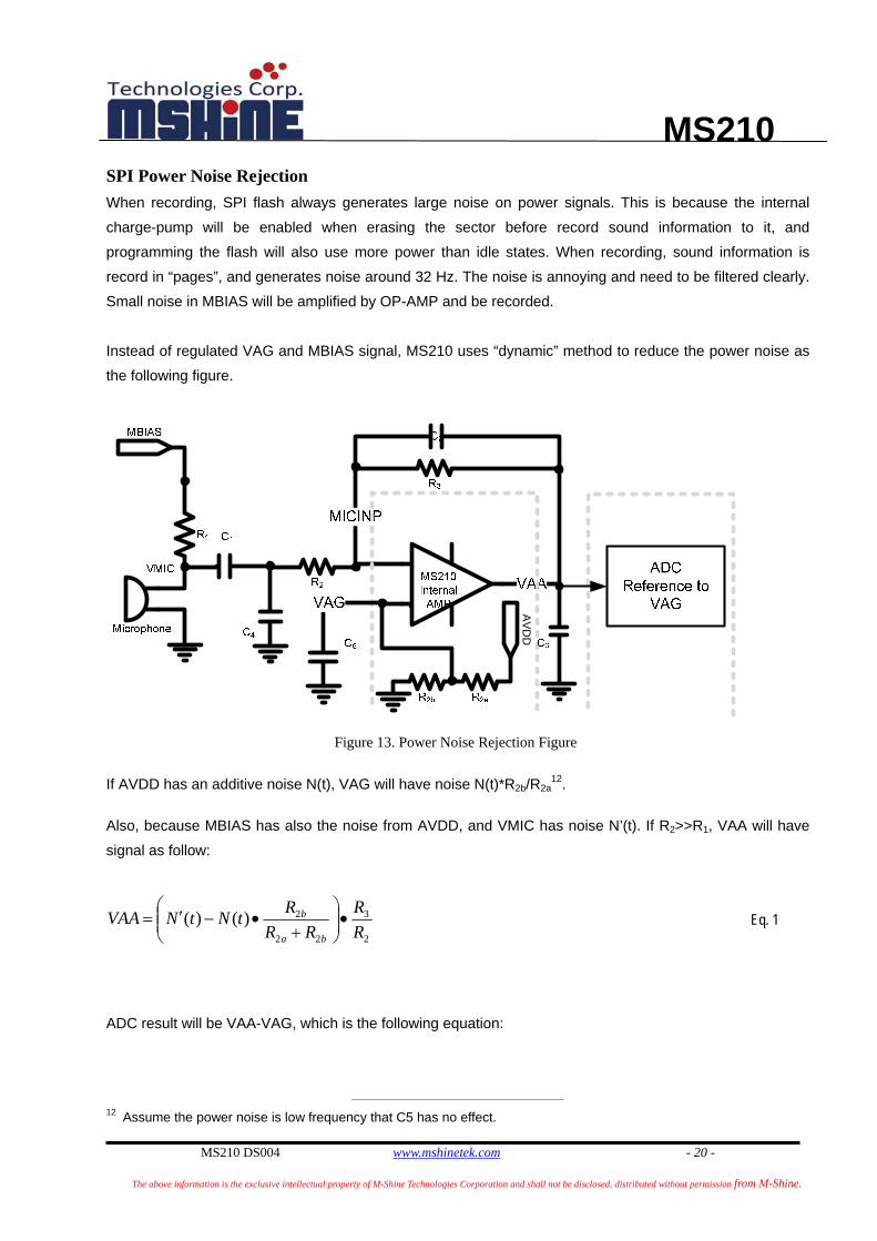
SPI Power Noise Rejection When recording, SPI flash always generates large noise on power signals. This is because the internal
charge-pump will be enabled when erasing the sector before record sound information to it, and
programming the flash will also use more power than idle states. When recording, sound information is
record in “pages”, and generates noise around 32 Hz. The noise is annoying and need to be filtered clearly.
Small noise in MBIAS will be amplified by OP-AMP and be recorded.
Instead of regulated VAG and MBIAS signal, MS210 uses “dynamic” method to reduce the power noise as
the following figure.
AVD
D
Figure 13. Power Noise Rejection Figure
If AVDD has an additive noise N(t), VAG will have noise N(t)*R2b/R2a
12.
Also, because MBIAS has also the noise from AVDD, and VMIC has noise N’(t). If R2>>R1, VAA will have
signal as follow:
2
3
22
2)()(RR
RRRtNtNVAA
ba
b •⎟⎟⎠
⎞⎜⎜⎝
⎛+
•−′= Eq. 1
ADC result will be VAA-VAG, which is the following equation:
12 Assume the power noise is low frequency that C5 has no effect.

MS210
MS210 DS004 www.mshinetek.com - 21 -
The above information is the exclusive intellectual property of M-Shine Technologies Corporation and shall not be disclosed, distributed without permission from M-Shine.
2
3
22
2
2
3
22
2
3
2
22
2
22
2
2
3
22
2
)()(
)()(
)()()(
RR
RRRtNtN
RR
RRR
RR
RRRtNtN
RRRtN
RR
RRRtNtNVADC
ba
b
ba
b
ba
b
ba
b
ba
b
•⎟⎟⎠
⎞⎜⎜⎝
⎛+
•−′≅
•⎟⎟⎠
⎞⎜⎜⎝
⎛⎟⎟⎠
⎞⎜⎜⎝
⎛+
•−+
•−′=
+•−•⎟⎟
⎠
⎞⎜⎜⎝
⎛+
•−′=
Eq. 2
Since R3/R2 is large, and R2/R3 is very small. We can consider only the large part. From Eq. 2, we know if
VADC will be almost zero if the following condition is true.
ba
b
RRRtNtN
22
2)()(+
•≅′ Eq. 3
That is, if the microphone’s impedance is “almost” resistive, we can assume that if DC of VMIC is equal to DC of VAG, the noise can be cancelled mostly. Because VMIC has noise from AVDD (MBIAS) around
N(t)*RMIC/(R1+RMIC). If that value is equal to VMIC, the DC values of them are almost the same.
Above theory applies when the noise on AVDD/AVSS is small and has very quiet and has few harmonic
power.
For NO-MIC recording applications, no power noise will be generated theoretically.
Playing Function Description MS210 can play the recorded sound from the SPI Flash memory. The following subsections will describe the
playing function in detail.
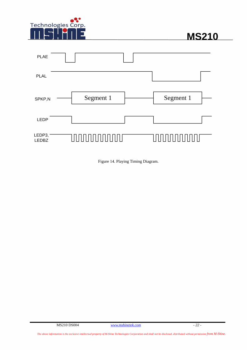
Playing Timing Diagram, 1-SEG Mode (SEG2 pin floating)
When PLAE or PLAL pressed, MS210 will start to play. The LED and sound segment timing is as the
following figure, when SEG2 pin is floating.
MS210
MS210 DS004 www.mshinetek.com - 22 -
The above information is the exclusive intellectual property of M-Shine Technologies Corporation and shall not be disclosed, distributed without permission from M-Shine.
PLAE
PLAL
SPKP,N Segment 1 Segment 1
LEDP
LEDP3,LEDBZ
Figure 14. Playing Timing Diagram.
MS210
MS210 DS004 www.mshinetek.com - 23 -
The above information is the exclusive intellectual property of M-Shine Technologies Corporation and shall not be disclosed, distributed without permission from M-Shine.
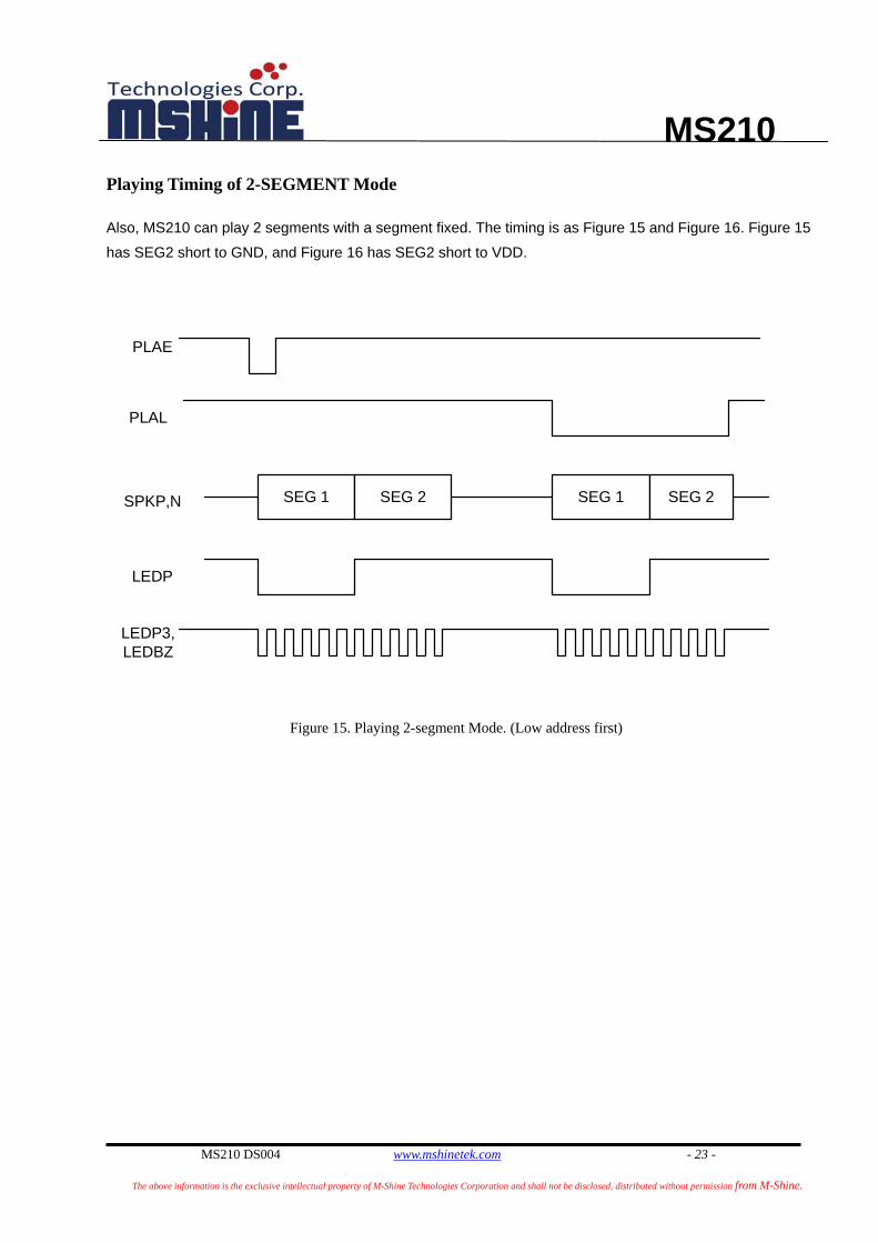
Playing Timing of 2-SEGMENT Mode Also, MS210 can play 2 segments with a segment fixed. The timing is as Figure 15 and Figure 16. Figure 15
has SEG2 short to GND, and Figure 16 has SEG2 short to VDD.
PLAE
PLAL
SPKP,N SEG 1
LEDP
LEDP3,LEDBZ
SEG 2 SEG 1 SEG 2
Figure 15. Playing 2-segment Mode. (Low address first)

MS210
MS210 DS004 www.mshinetek.com - 24 -
The above information is the exclusive intellectual property of M-Shine Technologies Corporation and shall not be disclosed, distributed without permission from M-Shine.
PLAE
PLAL
SPKP,N SEG 2
LEDP
LEDP3,LEDBZ
SEG 1 SEG 2 SEG 1
Figure 16. Playing 2-segment Mode. (High address first)
Note that LEDP low at only first segment. This can be used for different sample rate configuration for preload
song and recording voice. “Sample Rate and Resistor” Section has detailed description.
RECL over PLAL MS210 has a special function about the key buttons that PLAL function can be interrupted by RECL. That is,
when PLAL and RECL are low at the same time, RECL function will always overtake PLAL function. The
function is suitable for card applications that external photo resistor is only required at PLAL pad.
That is, if PLAL is low, PLAE and RECE keys will have no function. However, if RECL is low, MS210 will
change to recording mode, and when RECL is released, MS210 will play again the newly record segment.
After the new segment is played, MS210 will enter sleep mode even PLAL is low.
The timing diagram is as below:

MS210
MS210 DS004 www.mshinetek.com - 25 -
The above information is the exclusive intellectual property of M-Shine Technologies Corporation and shall not be disclosed, distributed without permission from M-Shine.
Recording New SegmentPLAL
RECL
SPKP,N Segment 1
LEDP
LEDP3
BEEP
New Segment
BEEP
LEDBZ
Figure 17. RECL interrupt PLAL function.
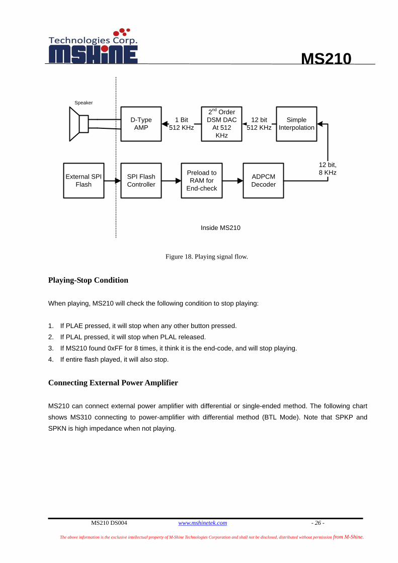
Signal Flow When Playing
When MS210 playing, the signal will be strait-forward as Figure 18. The data will be read from the SPI flash
and interpolated to the amplifier.
MS210
MS210 DS004 www.mshinetek.com - 26 -
The above information is the exclusive intellectual property of M-Shine Technologies Corporation and shall not be disclosed, distributed without permission from M-Shine.
2nd Order DSM DAC
At 512KHz
SimpleInterpolation
ADPCMDecoder
Preload to RAM for
End-check
SPI Flash Controller
External SPIFlash
12 bit512 KHz
12 bit,8 KHz
Inside MS210
D-TypeAMP
Speaker
1 Bit512 KHz
Figure 18. Playing signal flow.
Playing-Stop Condition
When playing, MS210 will check the following condition to stop playing:
1. If PLAE pressed, it will stop when any other button pressed.
2. If PLAL pressed, it will stop when PLAL released.
3. If MS210 found 0xFF for 8 times, it think it is the end-code, and will stop playing.
4. If entire flash played, it will also stop.
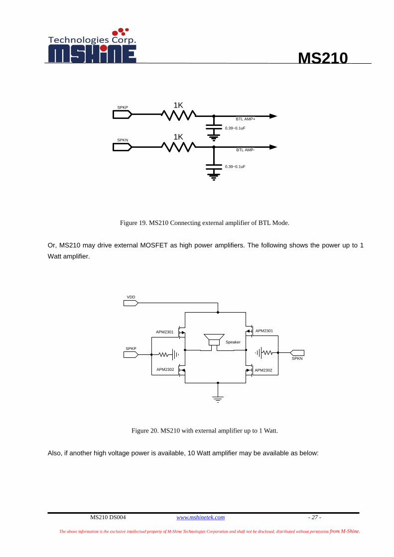
Connecting External Power Amplifier
MS210 can connect external power amplifier with differential or single-ended method. The following chart
shows MS310 connecting to power-amplifier with differential method (BTL Mode). Note that SPKP and
SPKN is high impedance when not playing.
MS210
MS210 DS004 www.mshinetek.com - 27 -
The above information is the exclusive intellectual property of M-Shine Technologies Corporation and shall not be disclosed, distributed without permission from M-Shine.
1K
1K
BTL AMP+
BTL AMP-
SPKP
SPKN
0.39~0.1uF
0.39~0.1uF
Figure 19. MS210 Connecting external amplifier of BTL Mode.
Or, MS210 may drive external MOSFET as high power amplifiers. The following shows the power up to 1
Watt amplifier.
Speaker
APM2301
APM2302
APM2301
APM2302
SPKP
SPKN
VDD
Figure 20. MS210 with external amplifier up to 1 Watt.
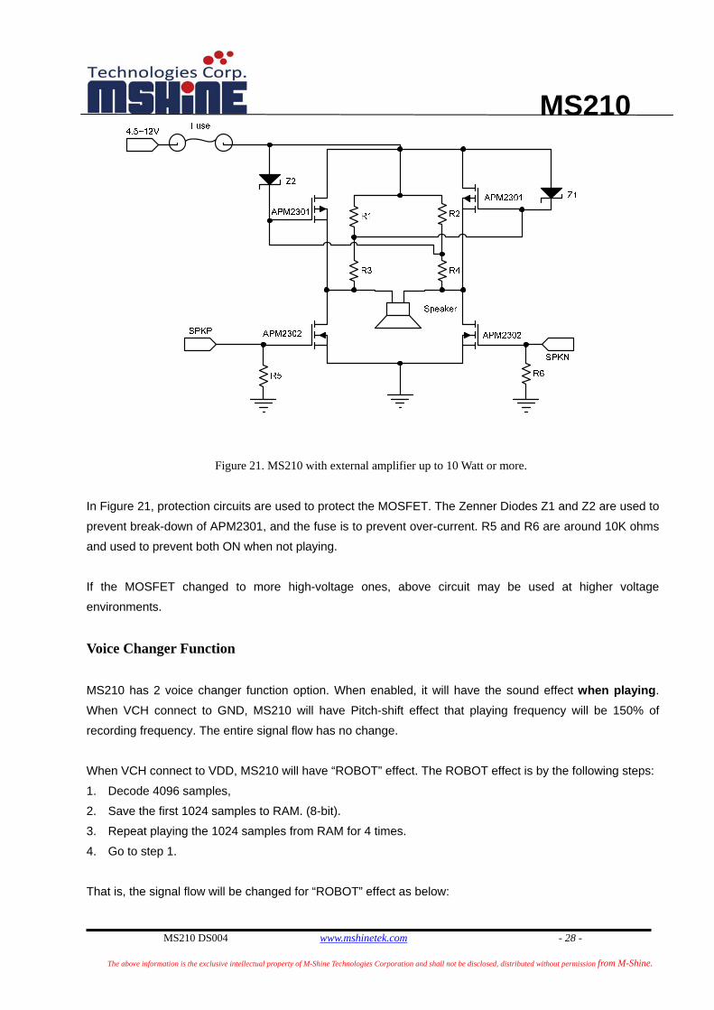
Also, if another high voltage power is available, 10 Watt amplifier may be available as below:
MS210
MS210 DS004 www.mshinetek.com - 28 -
The above information is the exclusive intellectual property of M-Shine Technologies Corporation and shall not be disclosed, distributed without permission from M-Shine.
Figure 21. MS210 with external amplifier up to 10 Watt or more.
In Figure 21, protection circuits are used to protect the MOSFET. The Zenner Diodes Z1 and Z2 are used to
prevent break-down of APM2301, and the fuse is to prevent over-current. R5 and R6 are around 10K ohms
and used to prevent both ON when not playing.
If the MOSFET changed to more high-voltage ones, above circuit may be used at higher voltage
environments.
Voice Changer Function
MS210 has 2 voice changer function option. When enabled, it will have the sound effect when playing.
When VCH connect to GND, MS210 will have Pitch-shift effect that playing frequency will be 150% of
recording frequency. The entire signal flow has no change.
When VCH connect to VDD, MS210 will have “ROBOT” effect. The ROBOT effect is by the following steps:
1. Decode 4096 samples,
2. Save the first 1024 samples to RAM. (8-bit).
3. Repeat playing the 1024 samples from RAM for 4 times.
4. Go to step 1.
That is, the signal flow will be changed for “ROBOT” effect as below:

MS210
MS210 DS004 www.mshinetek.com - 29 -
The above information is the exclusive intellectual property of M-Shine Technologies Corporation and shall not be disclosed, distributed without permission from M-Shine.
2nd Order DSM DAC
At 512KHz
SimpleInterpolation
ADPCMDecoder
RAMSPI Flash Controller
External SPIFlash
12 bit512 KHz
Inside MS210
D-TypeAMP
Speaker
1 Bit512 KHz
End code check Save the 1024 bytes of 4096 samples
RepeatThe 1024
Byte for 4 times
Figure 22. Signal Flow for ROBOT Effect.
The result recording and playing waveform will be like below:
Time
Recording Input Signal
Time
First1024
Samplesrepeated
Playing out signal
Figure 23. Example waveform of ROBOT Effect.

MS210
MS210 DS004 www.mshinetek.com - 30 -
The above information is the exclusive intellectual property of M-Shine Technologies Corporation and shall not be disclosed, distributed without permission from M-Shine.
ADPCM Coder and Decoder (CODEC)
MS210 has built-in ADPCM codec for saving the space of SPI Flash Memory. The CODEC is suitable for
speech signal. MSHINE provide a tool program that can code a sound file manually to MS210’s format and
can be used for 2-segment applications.
Note that coder and decoder can not work at the same time. MS210 will not enable CODEC in Pure-Amplifier
Mode.
Sample Rate and Resistor
For different sample rate, resistor of correct value should connect to OSCO pin. The recommend value is as
below (At 3.0V):
SAMPLE RATE (KHZ) 8.0 6.0 10.0 12.0 16.0
Typical
Resistor (K Ohms)
91 120 73 62 47
Double Sample Rate Configuration In 2 Segment mode, playing the “preload” segment may use different sample rate from default one. That is,
MS210 may play the preload song with higher sample rate and record the “high” address segment with lower
sample rate. The following configuration will have preload song played at 22 KHz and record/play the voice
at 12.0 KHz.
Figure 24. Example Double Sample Rate Configuration.

MS210
MS210 DS004 www.mshinetek.com - 31 -
The above information is the exclusive intellectual property of M-Shine Technologies Corporation and shall not be disclosed, distributed without permission from M-Shine.
Typical Application Circuits
Note: C1, C5, C4 is optional.
K3
PLAL
K2
RECE
K1
PLAE
10K
R5
0.1U
C6
CSB1
DO2
WPB3
GND4 DIO 5
CLK 6
HDB 7
VCC 8U1 MS25Xn0
DVDD SPICK
SPIMOSI
22P
C5
+1
-2
MIC1
MIC
R71K
R81K
LED4LEDP3
LED2LEDBZ
DVDD
K4
RECL
SPICS
SPIMISO
R122k
R61K
DVDD SPK1
SPEAKER
(1M,2M,4M,8M,16M,32M,64M)
DVDD1
DVSS2
AVDD3
AVSS4
OSCO5
TEST6
PLAE7
RECE8
PLAL9
RECL10
VCH11
BEEPEN12
SEG213 LEDP 14LEDP3 15LEDBZ 16SPICS 17SPICK 18SPIMOSI 19SPIMISO 20VAG 21VAA 22MBIAS 23MICINP 24SPKP 25SPKN 26U2
MS210
TESTPLAERECEPLALRECLVCHBEEPENSEG2
LEDP3 LEDBZ
LEDP
LEDBZSPICSSPICK
LEDP3
SPIMOSISPIMISO
MBIAS
VAG
LED3
LEDP
LEDP
22PC4
1.2M or 600KR2
1.5KR3
MBIASPLAE
RECE
PLAL
RECL470p
C1
DVDD
VDD
DVDD
CP1220UF
LED1LEDREC
R91K
LEDBZ
LEDP3
VAA
VDD
R4
10CP3100uF
GND
CP222uF
GND0.1uFC2
GND
BT1Battery 3V/4.5V
VDD
GND
MICINP0~10/0.5W
R10
R6A47k
PLALC1A0.1U
GND
Figure 25. Typical Application Circuit for Recording Application.
R122k
DVDD SPK1
SPEAKER
DVDD1
DVSS2
AVDD3
AVSS4
OSCO5
TEST6
PLAE7
RECE8
PLAL9
RECL10
VCH11
BEEPEN12
SEG213 LEDP 14LEDP3 15LEDBZ 16SPICS 17SPICK 18SPIMOSI 19SPIMISO 20VAG 21VAA 22MBIAS 23MICINP 24SPKP 25SPKN 26U2
MS210
TESTPLAERECEPLALRECLVCHBEEPENSEG2 LEDP
LEDBZSPICSSPICK
LEDP3
SPIMOSISPIMISO
MBIAS
VAG
470p
C1
VDD
DVDDCP1220UF
VAA
VDD
0.1uFC2
GND
MICINP
0.1U
C6Filter
C5
22PC4
R2
Gain
J?
Phonejack2
10K
R5
R?
0~10/0.5W
R6A47k
PLAL
Figure 26. Typical Application for simple Amplifier.
MS210
MS210 DS004 www.mshinetek.com - 32 -
The above information is the exclusive intellectual property of M-Shine Technologies Corporation and shall not be disclosed, distributed without permission from M-Shine.
K3
PLAL
K2
RECE
K1
PLAE
1K
R5
1U
C6
CSB1
DO2
WPB3
GND4 DIO 5
CLK 6
HDB 7
VCC 8U1 MS25Xn0
DVDD SPICK
SPIMOSIR71K
R81K
LED4LEDP3
LED2LEDBZ
DVDD
K4
RECL
SPICS
SPIMISO
R122k
R61K
DVDD SPK1
SPEAKER
(1M,2M,4M,8M,16M,32M,64M)
DVDD1
DVSS2
AVDD3
AVSS4
OSCO5
TEST6
PLAE7
RECE8
PLAL9
RECL10
VCH11
BEEPEN12
SEG213 LEDP 14LEDP3 15LEDBZ 16SPICS 17SPICK 18SPIMOSI 19SPIMISO 20VAG 21VAA 22MBIAS 23MICINP 24SPKP 25SPKN 26U2
MS210
TESTPLAERECEPLALRECLVCHBEEPENSEG2
LEDP3 LEDBZ
LEDP
LEDBZSPICSSPICK
LEDP3
SPIMOSISPIMISO
MBIAS
VAG
LED3
LEDP
LEDP
C40.1U
1.2M or 600K
R2PLAE
RECE
PLAL
RECL470p
C1
DVDD
VDD
DVDD
CP1220UF
LED1LEDREC
R91K
LEDBZ
LEDP3
VAA
VDD
R4
10CP3100uF
GND
0.1uFC2
GND
BT1Battery 3V/4.5V
VDD
GND
MICINP0~10/0.5W
R10SPKPSPKN
30
R3
30
R11
SPKP
R6A47k
PLALC1A0.1U
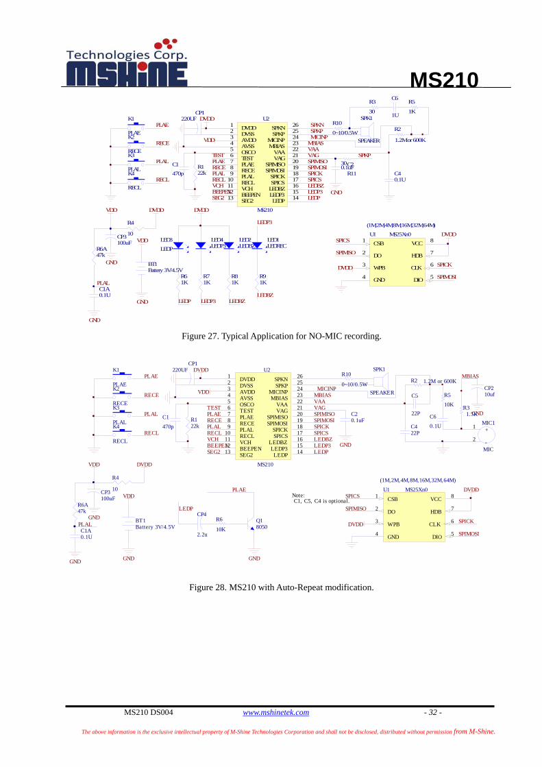
GND Figure 27. Typical Application for NO-MIC recording.
Note: C1, C5, C4 is optional.
K3
PLAL
K2
RECE
K1
PLAE
10K
R5
0.1U
C6
CSB1
DO2
WPB3
GND4 DIO 5
CLK 6
HDB 7
VCC 8U1 MS25Xn0
DVDD SPICK
SPIMOSI
22P
C5
+1
-2
MIC1
MIC
K4
RECL
SPICS
SPIMISO
R122k
DVDD SPK1
SPEAKER
(1M,2M,4M,8M,16M,32M,64M)
DVDD1
DVSS2
AVDD3
AVSS4
OSCO5
TEST6
PLAE7
RECE8
PLAL9
RECL10
VCH11
BEEPEN12
SEG213 LEDP 14LEDP3 15LEDBZ 16SPICS 17SPICK 18SPIMOSI 19SPIMISO 20VAG 21VAA 22MBIAS 23MICINP 24SPKP 25SPKN 26U2
MS210
TESTPLAERECEPLALRECLVCHBEEPENSEG2 LEDP
LEDBZSPICSSPICK
LEDP3
SPIMOSISPIMISO
MBIAS
VAG
22PC4
1.2M or 600KR2
1.5KR3
MBIASPLAE
RECE
PLAL
RECL470p
C1
DVDD
VDD
DVDD
CP1220UF
VAA
VDD
R4
10CP3100uF
GND
CP210uf
GND0.1uFC2
GND
BT1Battery 3V/4.5V
VDD
GND
MICINP0~10/0.5W
R10
Q18050
GND
CP4
2.2u10K
R6
PLAE
LEDPR6A47k
PLALC1A0.1U
GND
Figure 28. MS210 with Auto-Repeat modification.

MS210
MS210 DS004 www.mshinetek.com - 33 -
The above information is the exclusive intellectual property of M-Shine Technologies Corporation and shall not be disclosed, distributed without permission from M-Shine.
Absolute Maximum Ratings CommentsDC Supply Voltage.................-0.5V to + 4.5V Input Voltage.…………..-0.5V to VDD + 0.5V Output Voltage…………-0.5V to VDD + 0.5V Operating Temperature…...........-40° to 85° C Storage Temperature………..-70° to 150° C
Never allow a stress to exceed the values listed under “Absolute Maximum Ratings”, otherwise the device would suffer from a permanent damage. Nor is a stress at the listed value be allowed to persist over a period, since an extended exposure to the absolute maximum rating condition may also affect the reliability of the device, if not causing a damage thereof.
AC & DC Electrical Characteristics DC Characteristics Parameters Conditions Symbol Min. Typ. Max. Unit
With SPI flash working at 4.5V VDD 2.213 3.3 4.514 V
VDD Before Power ON VDDOFF 0.3 V
Supply voltage
VDD Rise Time TVDDR 200 ms
8KHz, recording, VDD=3.0V IREC 10 mA 8KHz, playing, VDD=3.0V, 8-Ohm speaker
IPLA 20 mA
Power-Down Mode, 3.0V15 IDD1 2 10 uA Power-Down Mode, 3.6V IDD2 7 uA
Supply Current
Power-Down Mode, 4.5V IDD3 100 uA I OH=1, Push-pull pins. VOH1 VDD-0.
2 - - V
Output voltage I OL=2 mA, push-pull pins VOL1 0.2 - - V
All Input Pins VIH1 0.8 VDD - VDD+0.3 V Input voltage16 All Input Pins VIL1 -0.3 - 0.2 VDD V
LED pins, VOL=0.5V, VOH=VDD-0.5V
IOL1 IOH1
8
-8 mA
AMP pins, 8-ohm speaker connected IOL2 IOH2
-100 +100
mA
KEY pulled high input at 4.5V IPH -0.9 mA
Output current
KEY pulled high input at 3.6V IPH -0.6 mA
MBIAS Output Current
VDD=3.3V Imbo 3 mA
VAG output Voltage
VDD=3.3V Vag 0.9 V
13 The supply voltage MUST be greater than the working voltage of the SPI Flash Memory. 14 When VDD>=3.3V, 8-ohm speaker must be connected with a resistor and an inductor. 15 SPI Flash’s power is not included. 16 Schemitter Trigger level around 2VDD/5, 3VDD/5 is implemented for all input pins.

MS210
MS210 DS004 www.mshinetek.com - 34 -
The above information is the exclusive intellectual property of M-Shine Technologies Corporation and shall not be disclosed, distributed without permission from M-Shine.
POR Release voltage
Temp=23° C Vpor 1.8 V
Table 3. DC Characteristics of MS210.
AC Characteristics Parameters Conditions Symbol Min. Typ. Max. Unit Key button De-bounce time
Sample Rate = 8.0 KHz Tkd 30 ms
ADC Input Range17
VDD=2.3~4.5V Vadi 0.25 2.25 VDC
External RC Frequency
VDD=2.3~4.5V Frc 8 MHz
ADC Sample rate18
VDD=3.0V FS 6 8 16 KHz
Speech Signal SNR
VDD=3.0V ADCSNR 6019 DB
Speech Dynamic Range
VDD=3.0V ADCSNDR 70 DB
MBIAS Driving Current
VDD=3.0V IMBIAS 2 MA
ADC POWER NOISE REJECT
VDD=3.0V PSRR 50 DB
ADC COMMON MODE REJECT
VDD=3.0V CMRR 40 DB
Input OPA Open loop gain
VDD=3.0v GOL 70 DB
OPA Input offset
VDD=3.0V Oop 10 mV
OPA Unit gain bandwidth
VDD=3.0V BWuni 1 MHz
MBIAS Power Noise Reject Ratio20
VDD=3.3V,load=2.0 mA PSRRmb 15 db
Table 4. AC Characteristics.
17 ADC input will be DC offset to VAG by OPA inside, which is usually VDD/2. 18 ADC Sample rate is limited by the sector-erase time with the memory since higher frequency needs more data stored
at RAM when SPI is under sector-erase. The sample rate limit is [2560/sector-erase-time]. That is, sound sample will be
dropped while recording if sample rate is greater than [2560/sector-erase-time]. 19 Input signal is around 100 Hz sine wave. 20 Without capacitor.

MS210
MS210 DS004 www.mshinetek.com - 35 -
The above information is the exclusive intellectual property of M-Shine Technologies Corporation and shall not be disclosed, distributed without permission from M-Shine.
Package Outline