mram preso final for web - nxp semiconductors...2003 functionality was demonstrated on customer’s...
TRANSCRIPT
TM
Freescale™ and the Freescale logo are trademarks of Freescale Semiconductor, Inc. All other product or service names are the property of their respective owners. © Freescale Semiconductor, Inc. 2006.
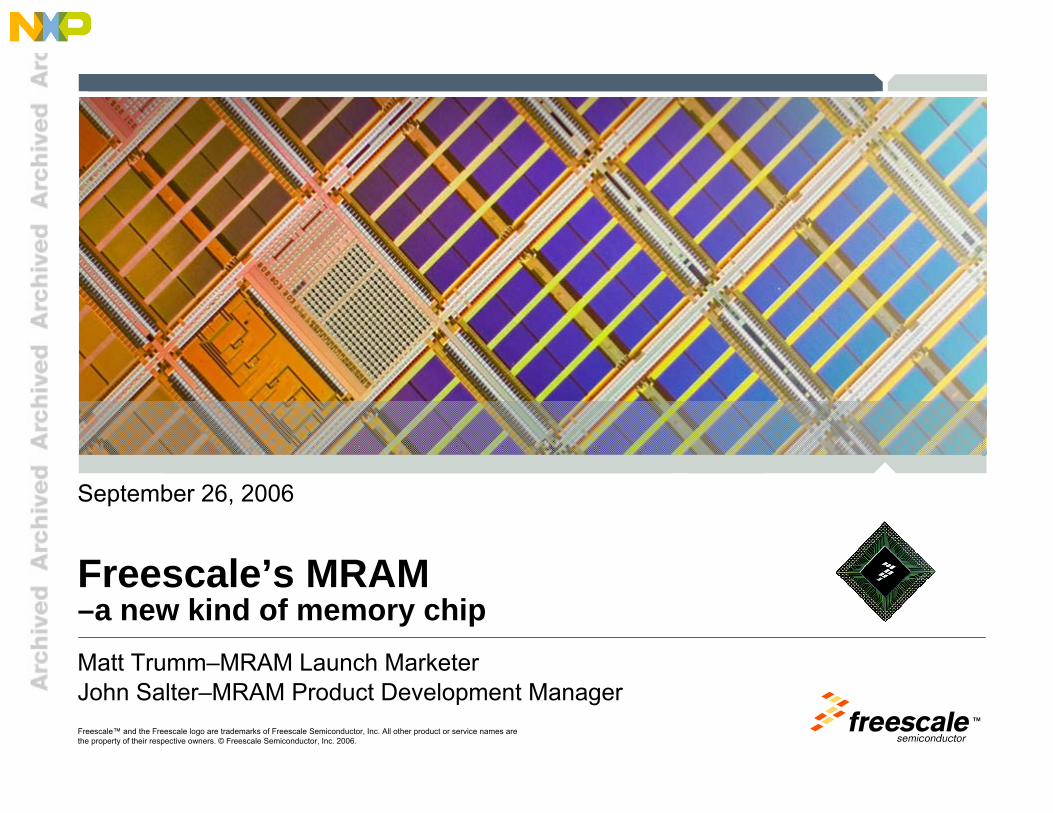
Freescale’s MRAM –a new kind of memory chip
September 26, 2006
Matt Trumm–MRAM Launch MarketerJohn Salter–MRAM Product Development Manager
TMFreescale™ and the Freescale logo are trademarks of Freescale Semiconductor, Inc. All other product or service names are the property of their respective owners. © Freescale Semiconductor, Inc. 2006. 1
Agenda
► Freescale’s MRAM
• What is it?
• How does it work?
• Why is it better than existing memory solutions?
• When will it be available?
TMFreescale™ and the Freescale logo are trademarks of Freescale Semiconductor, Inc. All other product or service names are the property of their respective owners. © Freescale Semiconductor, Inc. 2006. 2
What is it?
TMFreescale™ and the Freescale logo are trademarks of Freescale Semiconductor, Inc. All other product or service names are the property of their respective owners. © Freescale Semiconductor, Inc. 2006. 3
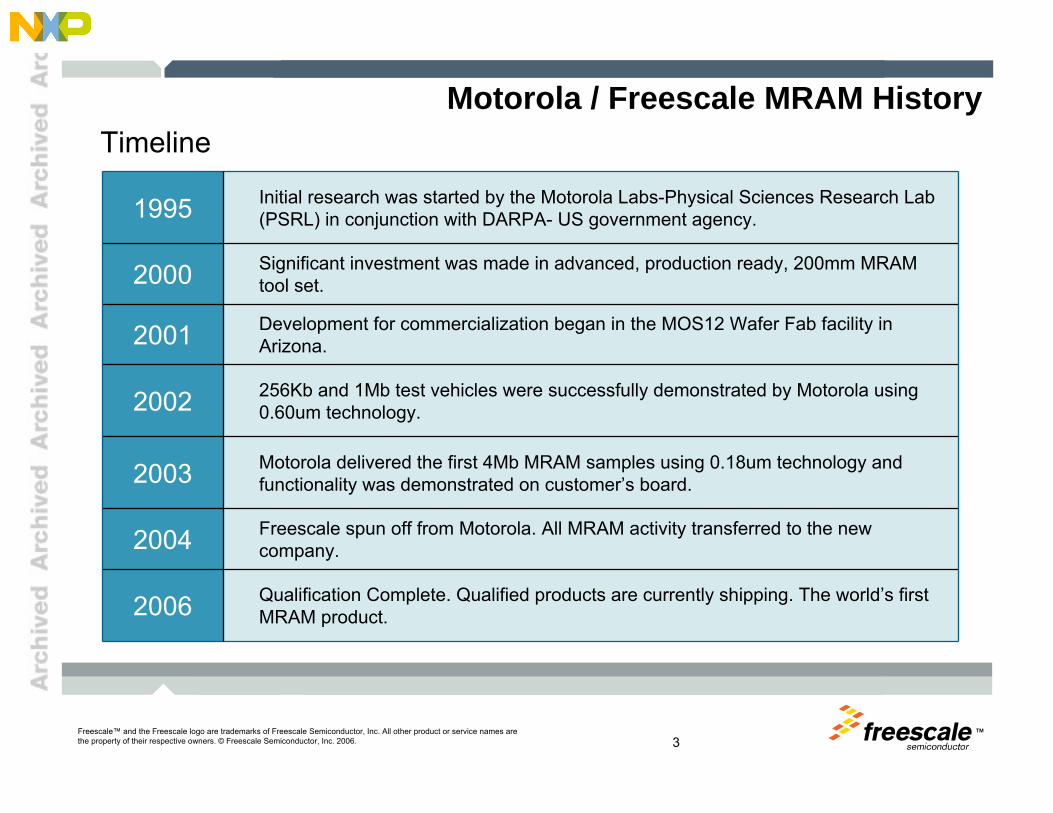
Motorola / Freescale MRAM History
Qualification Complete. Qualified products are currently shipping. The world’s first MRAM product.2006
Freescale spun off from Motorola. All MRAM activity transferred to the new company.2004
Motorola delivered the first 4Mb MRAM samples using 0.18um technology and functionality was demonstrated on customer’s board.2003
256Kb and 1Mb test vehicles were successfully demonstrated by Motorola using 0.60um technology.2002
Development for commercialization began in the MOS12 Wafer Fab facility in Arizona.2001
Significant investment was made in advanced, production ready, 200mm MRAM tool set.2000
Initial research was started by the Motorola Labs-Physical Sciences Research Lab (PSRL) in conjunction with DARPA- US government agency.1995
Timeline
TMFreescale™ and the Freescale logo are trademarks of Freescale Semiconductor, Inc. All other product or service names are the property of their respective owners. © Freescale Semiconductor, Inc. 2006. 4
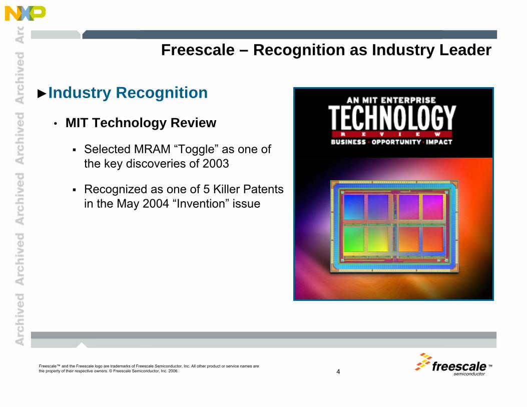
►Industry Recognition
• MIT Technology Review
Selected MRAM “Toggle” as one of the key discoveries of 2003
Recognized as one of 5 Killer Patents in the May 2004 “Invention” issue
Freescale – Recognition as Industry Leader
TMFreescale™ and the Freescale logo are trademarks of Freescale Semiconductor, Inc. All other product or service names are the property of their respective owners. © Freescale Semiconductor, Inc. 2006. 5
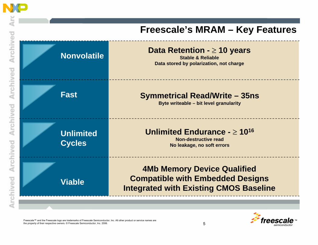
Data Retention - ≥ 10 yearsStable & Reliable
Data stored by polarization, not charge
Symmetrical Read/Write – 35nsByte writeable – bit level granularity
Unlimited Endurance - ≥ 1016Non-destructive read
No leakage, no soft errors
4Mb Memory Device QualifiedCompatible with Embedded Designs
Integrated with Existing CMOS Baseline
Freescale’s MRAM – Key Features
Nonvolatile
Fast
Unlimited Cycles
Viable
TMFreescale™ and the Freescale logo are trademarks of Freescale Semiconductor, Inc. All other product or service names are the property of their respective owners. © Freescale Semiconductor, Inc. 2006. 6
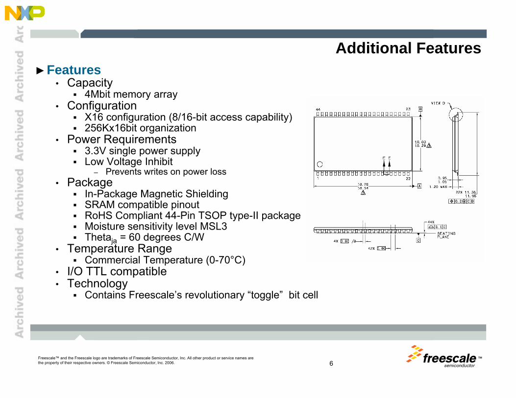
Additional Features►Features
• Capacity4Mbit memory array
• ConfigurationX16 configuration (8/16-bit access capability)256Kx16bit organization
• Power Requirements3.3V single power supplyLow Voltage Inhibit
– Prevents writes on power loss• Package
In-Package Magnetic ShieldingSRAM compatible pinout RoHS Compliant 44-Pin TSOP type-II packageMoisture sensitivity level MSL3Thetaja = 60 degrees C/W
• Temperature RangeCommercial Temperature (0-70°C)
• I/O TTL compatible• Technology
Contains Freescale’s revolutionary “toggle” bit cell
TMFreescale™ and the Freescale logo are trademarks of Freescale Semiconductor, Inc. All other product or service names are the property of their respective owners. © Freescale Semiconductor, Inc. 2006. 7
How Does it Work?
TMFreescale™ and the Freescale logo are trademarks of Freescale Semiconductor, Inc. All other product or service names are the property of their respective owners. © Freescale Semiconductor, Inc. 2006. 8
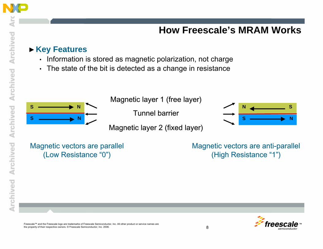
Magnetic vectors are parallel(Low Resistance “0”)
Magnetic vectors are anti-parallel (High Resistance “1”)
►Key Features• Information is stored as magnetic polarization, not charge• The state of the bit is detected as a change in resistance
Magnetic layer 1 (free layer)
Magnetic layer 2 (fixed layer)
Tunnel barrierS
S N
N N
S N
S
How Freescale’s MRAM Works
TMFreescale™ and the Freescale logo are trademarks of Freescale Semiconductor, Inc. All other product or service names are the property of their respective owners. © Freescale Semiconductor, Inc. 2006. 9
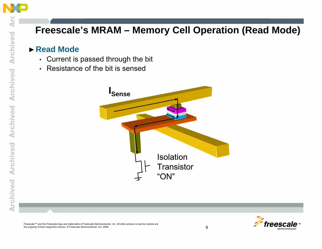
Isolation Transistor“ON”
ISense
►Read Mode• Current is passed through the bit• Resistance of the bit is sensed
Freescale’s MRAM – Memory Cell Operation (Read Mode)
TMFreescale™ and the Freescale logo are trademarks of Freescale Semiconductor, Inc. All other product or service names are the property of their respective owners. © Freescale Semiconductor, Inc. 2006. 10
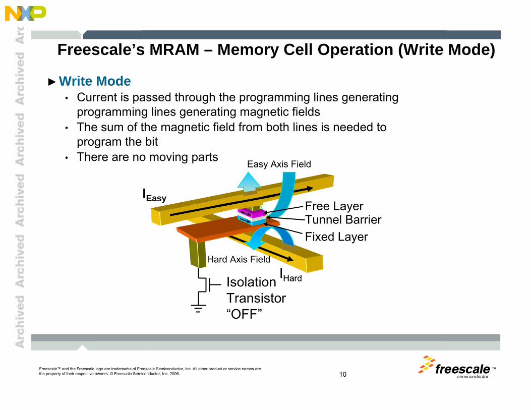
Free LayerTunnel BarrierFixed Layer
Easy Axis Field
Hard Axis Field
Isolation Transistor“OFF”
IEasy
IHard
►Write Mode• Current is passed through the programming lines generating
programming lines generating magnetic fields• The sum of the magnetic field from both lines is needed to
program the bit• There are no moving parts
Freescale’s MRAM – Memory Cell Operation (Write Mode)
TMFreescale™ and the Freescale logo are trademarks of Freescale Semiconductor, Inc. All other product or service names are the property of their respective owners. © Freescale Semiconductor, Inc. 2006. 11
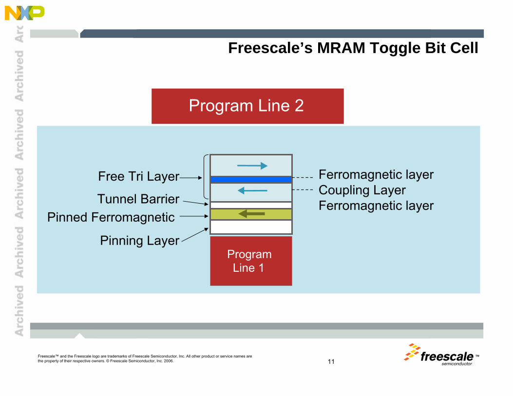
Freescale’s MRAM Toggle Bit Cell
Bit Line
DL Program Line
BL Program LineBit Line
Program Line 1
Program Line 2
Free Tri Layer
Tunnel BarrierPinned Ferromagnetic
Pinning Layer
Ferromagnetic layerCoupling LayerFerromagnetic layer
TMFreescale™ and the Freescale logo are trademarks of Freescale Semiconductor, Inc. All other product or service names are the property of their respective owners. © Freescale Semiconductor, Inc. 2006. 12
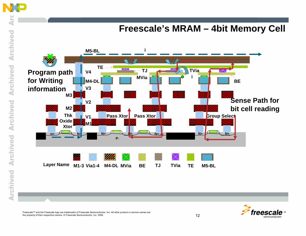
M5-BLVia1-4M1-3
N+P-
Layer Name
N+ N+
M4-DL MVia BE TVia TETJ
N+ N+N+ N+
M1
M3
M2
M4-DL
V1
V2
V3
V4MVia
BE
TETJ TVia
M5-BL
Group SelectPass Xtor Pass XtorThk Oxide
Xtor
i
i
Program path for Writing information
Sense Path for bit cell reading
Freescale’s MRAM – 4bit Memory Cell
TMFreescale™ and the Freescale logo are trademarks of Freescale Semiconductor, Inc. All other product or service names are the property of their respective owners. © Freescale Semiconductor, Inc. 2006. 13
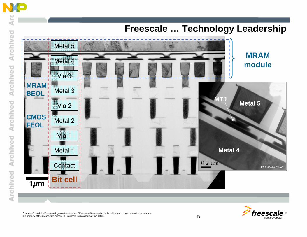
Freescale … Technology Leadership
MRAM BEOL
CMOS FEOL
Contact
Via 1
Metal 2
Metal 1
Via 2
Metal 4
Bit cell
Via 3
Metal 5
Metal 3MTJ
Metal 4
Metal 5
MRAM module
TMFreescale™ and the Freescale logo are trademarks of Freescale Semiconductor, Inc. All other product or service names are the property of their respective owners. © Freescale Semiconductor, Inc. 2006. 14
Why is it Better than Existing Memory Solutions?
TMFreescale™ and the Freescale logo are trademarks of Freescale Semiconductor, Inc. All other product or service names are the property of their respective owners. © Freescale Semiconductor, Inc. 2006. 15
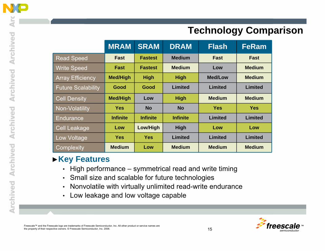
Technology Comparison
►Key Features• High performance – symmetrical read and write timing• Small size and scalable for future technologies• Nonvolatile with virtually unlimited read-write endurance• Low leakage and low voltage capable
Low
Yes
Low/High
Infinite
No
Low
Good
High
Fastest
Fastest
SRAM
MediumMediumMediumMediumComplexity
LimitedLimitedLimitedYesLow Voltage
LowLowHighLowCell Leakage
LimitedLimitedInfiniteInfiniteEndurance
YesYesNoYesNon-Volatility
MediumMediumHighMed/HighCell Density
LimitedLimitedLimitedGoodFuture Scalability
MediumMed/LowHighMed/HighArray Efficiency
MediumLowMediumFastWrite Speed
FastFastMediumFastRead Speed
FeRamFlashDRAMMRAM
TMFreescale™ and the Freescale logo are trademarks of Freescale Semiconductor, Inc. All other product or service names are the property of their respective owners. © Freescale Semiconductor, Inc. 2006. 16
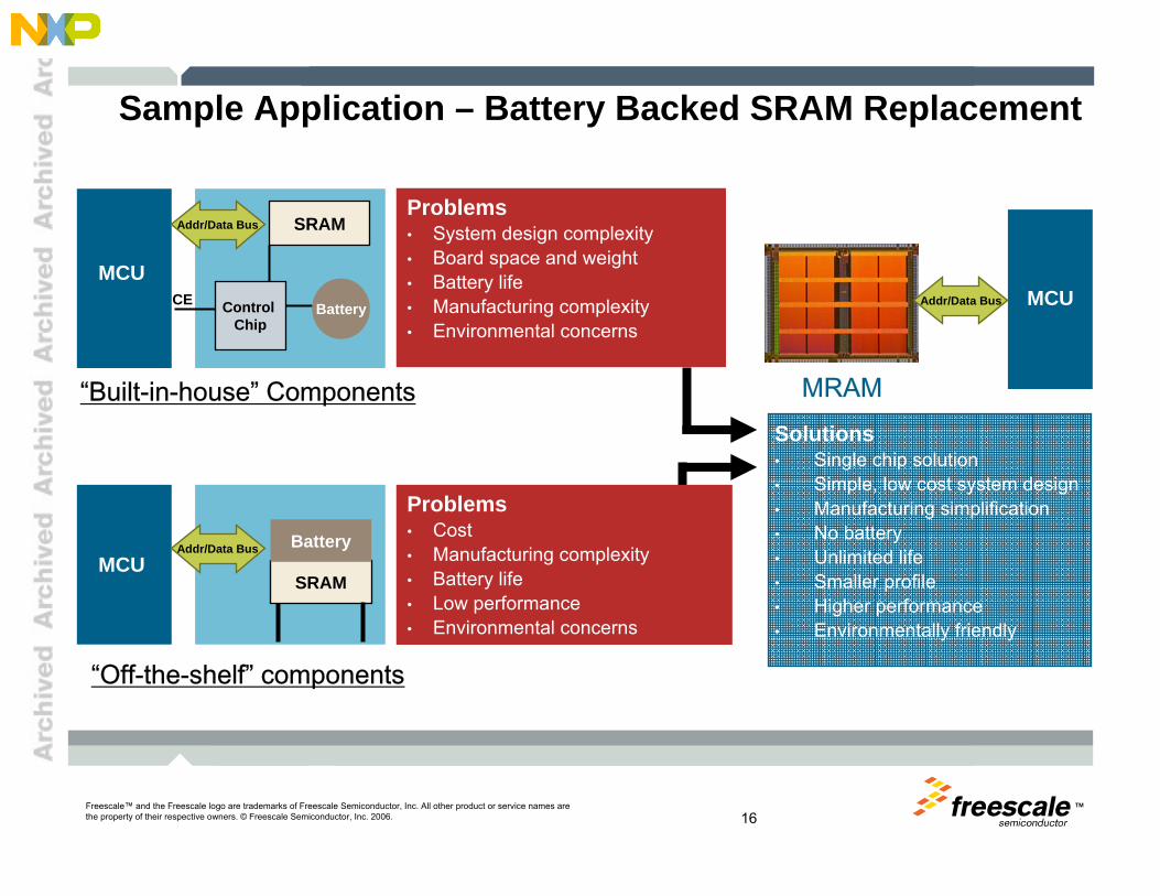
MCU
SRAM
BatteryControl Chip
CE
Problems• System design complexity• Board space and weight• Battery life• Manufacturing complexity• Environmental concerns
MRAMSolutions• Single chip solution• Simple, low cost system design• Manufacturing simplification• No battery• Unlimited life• Smaller profile • Higher performance• Environmentally friendly
“Built-in-house” Components
MCUSRAM
Battery
Problems• Cost• Manufacturing complexity• Battery life• Low performance• Environmental concerns
“Off-the-shelf” components
Addr/Data Bus
Sample Application – Battery Backed SRAM Replacement
Addr/Data Bus
Addr/Data Bus MCU
TMFreescale™ and the Freescale logo are trademarks of Freescale Semiconductor, Inc. All other product or service names are the property of their respective owners. © Freescale Semiconductor, Inc. 2006. 17
When Will it be Available?
TMFreescale™ and the Freescale logo are trademarks of Freescale Semiconductor, Inc. All other product or service names are the property of their respective owners. © Freescale Semiconductor, Inc. 2006. 18
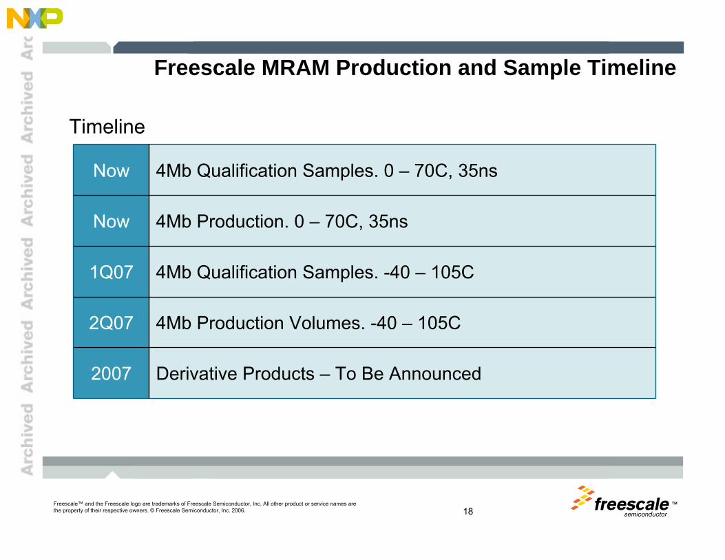
Freescale MRAM Production and Sample Timeline
Derivative Products – To Be Announced2007
4Mb Production Volumes. -40 – 105C2Q07
4Mb Qualification Samples. -40 – 105C1Q07
4Mb Production. 0 – 70C, 35nsNow
4Mb Qualification Samples. 0 – 70C, 35nsNow
Timeline
TMFreescale™ and the Freescale logo are trademarks of Freescale Semiconductor, Inc. All other product or service names are the property of their respective owners. © Freescale Semiconductor, Inc. 2006. 19
Q&A
John Salter –MRAM Product Development Manager
TMFreescale™ and the Freescale logo are trademarks of Freescale Semiconductor, Inc. All other product or service names are the property of their respective owners. © Freescale Semiconductor, Inc. 2006. 20
Thank YouTo learn more about MRAM please contactJohn Salter at [email protected]
or visitwww.freescale.com/mram
TMFreescale™ and the Freescale logo are trademarks of Freescale Semiconductor, Inc. All other product or service names are the property of their respective owners. © Freescale Semiconductor, Inc. 2006. 21
TM