mpt612 maximum power point tracking ic · pdf filenxp semiconductors mpt612 maximum power...
TRANSCRIPT

MPT612 Maximum power point tracking IC Rev. 2 — 14 September 2010 Product data sheet
1. General description The MPT612, the first dedicated IC for performing the Maximum Power Point Tracking (MPPT) function, is designed for use in applications that use solar photovoltaic (PV) cells or in fuel cells. To simplify development and maximize system efficiency, the MPT612 is supported by a patent-pending MPPT algorithm, an application-specific software library and easy-to-use application programming interfaces (APIs). Dedicated hardware functions for PV panels, including voltage and current measurement and panel parameter configuration, simplify design and speed development.
The MPT612 is based on a low-power ARM7TDMI-S RISC processor that operates at up to 70 MHz and can achieve system efficiency ratings up to 98 %. It controls the external switching device through a signal derived from a patent-pending MPPT algorithm. The DC source can be connected to the IC through appropriate voltage and current sensors. The IC dynamically extracts the maximum power from the DC source, without user intervention. The IC can be configured for boundary conditions set in software. There are up to 15 kB of flash memory available for application software.
In this datasheet, solar PV terminology has been primarily used as an example. However, the MPT612 is equally useful for fuel cells or any other DC source which has MPP behavior.

NXP Semiconductors MPT612 Maximum power point tracking IC
2. Features and benefits ARM7TDMI-S 32 bit RISC core operating at up to 70 MHz 128-bit wide interface and accelerator enabling 70 MHz operation 10-bit ADC providing
Eight analog inputs Conversion times as low as 2.44 µs per channel and dedicated result registers minimize interrupt overhead Five analog inputs available for user specific applications
One 32-bit timer and external event counter with four capture and four compare channels
One 16-bit timer and external event counter with three compare channels Low power Real-Time Clock (RTC) with independent power supply and dedicated
32 kHz clock input Serial interfaces including:
Two UARTs (16C550) Two Fast I2C-buses (400 kbit/s) SPI and SSP with buffering and variable data length capabilities
Vectored interrupt controller with configurable priorities and vector addresses Up to twenty eight (28), 5 V tolerant fast general purpose I/O pins Up to 13 edge or level sensitive external interrupt pins available Three levels of flash Code Read Protection (CRP) 70 MHz maximum clock available from programmable on-chip PLL with input
frequencies between 10 MHz and 25 MHz and a settling time of 100 ms Integrated oscillator operates with an external crystal at between 1 MHz and 25 MHz Power saving modes include:
Idle mode Two Power-down modes; one with the RTC active and with the RTC deactivated
Individual enabling/disabling of peripheral functions and peripheral clock scaling for additional power optimization
Processor wake-up from Power-down and Deep power-down mode using an external interrupt or the RTC
3. Applications DC application charge controller for solar PV power and fuel-cells. The use cases are
Battery charging for home appliances such as lighting, DC fans, DC TV,DC motor or any other DC appliance Battery charging for public lighting and signaling - LED street lighting, garden/driveway lighting, railway signaling, traffic signaling, remote telecom terminals/towers etc Battery charging for portable devices
DC-DC converter per panel to provide improved efficiency Micro inverter per panel removes the need for one large system inverter
MPT612 All information provided in this document is subject to legal disclaimers. © NXP B.V. 2010. All rights reserved.
Product data sheet Rev. 2 — 14 September 2010 2 of 2

NXP Semiconductors MPT612 Maximum power point tracking IC
4. Ordering information
Table 1. Ordering information Type number Package
Name Description Version MPT612FBD48 LQFP48 plastic low profile quad flat package; 48 leads; body 7 × 7 × 1.4 mm SOT313-2
5. Block diagram
001aam089
PV VOLTAGEMEASUREMENT
PV voltage sense
PV CURRENTMEASUREMENT
PV current sense
BATTERY VOLTAGEMEASUREMENT
battery voltage sense
BATTERY CURRENTMEASUREMENT
battery current sense
TEMPERATUREMEASUREMENT
temperature sense
LOAD CURRENTMEASUREMENT
these blocks are needed for MPPT functionality
these blocks can be used for customer specific application
PV CONFIGURATIONBLOCK
MPT612
MPPT ALOGIRTHM
BATTERY CHARGECYCLE ALGORITHM
BATTERYCONFIGURATION BLOCK
LOAD MANAGEMENT
LOAD CONFIGURATIONBLOCK
load configurationparameters
battery configurationparameters
STATUS INDICATION
PV configuration parameters
SWITCH CIRCUITCONTROL
BATTERYPROTECTION BLOCK
LOAD PROTECTION
LEDs
PWM
battery
load
load current sense
The configuration parameters are determined using the software
Fig 1. Block diagram
MPT612 All information provided in this document is subject to legal disclaimers. © NXP B.V. 2010. All rights reserved.
Product data sheet Rev. 2 — 14 September 2010 3 of 3
NXP Semiconductors MPT612 Maximum power point tracking IC
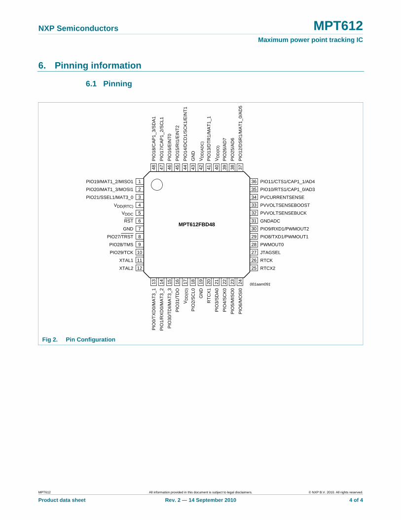
6. Pinning information
6.1 Pinning
Fig 2. Pin Configuration
MPT612FBD48
PIO19/MAT1_2/MISO1 PIO11/CTS1/CAP1_1/AD4
PIO20/MAT1_3/MOSI1 PIO10/RTS1/CAP1_0/AD3
PIO21/SSEL1/MAT3_0 PVCURRENTSENSE
VDD(RTC) PVVOLTSENSEBOOST
VDDC PVVOLTSENSEBUCK
RST GNDADC
GND PIO9/RXD1/PWMOUT2
PIO27/TRST PIO8/TXD1/PWMOUT1
PIO28/TMS PWMOUT0
PIO29/TCK JTAGSEL
XTAL1 RTCK
XTAL2 RTCX2
PIO
18/C
AP
1_3/
SD
A1
PIO
17/C
AP
1_2/
SC
L1
PIO
16/E
INT
0
PIO
15/R
I1/E
INT
2
PIO
14/D
CD
1/S
CK
1/E
INT
1
GN
D
VD
D(A
DC
)
PIO
13/D
TR
1/M
AT
1_1
VD
D(I
O)
PIO
26/A
D7
PIO
25/A
D6
PIO
12/D
SR
1/M
AT
1_0/
AD
5
PIO
0/T
XD
0/M
AT
3_1
PIO
1/R
XD
0/M
AT
3_2
PIO
30/T
DI/M
AT
3_3
PIO
31/T
DO
VD
D(I
O)
PIO
2/S
CL0
GN
D
RT
CX
1
PIO
3/S
DA
0
PIO
4/S
CK
0
PIO
5/M
ISO
0
PIO
6/M
OS
I0
001aam091
1
2
3
4
5
6
7
8
9
10
11
12
36
35
34
33
32
31
30
29
28
27
26
25
13 14 15 16 17 18 19 20 21 22 23
48 47 46 45 44 43 42 41 40 39 38 3724
MPT612 All information provided in this document is subject to legal disclaimers. © NXP B.V. 2010. All rights reserved.
Product data sheet Rev. 2 — 14 September 2010 4 of 4

NXP Semiconductors MPT612 Maximum power point tracking IC
MPT612 All information provided in this document is subject to legal disclaimers. © NXP B.V. 2010. All rights reserved.
Product data sheet Rev. 2 — 14 September 2010 5 of 5
6.2 Pin description
Table 2. Pin description Symbol Pin Type Description PIO0 to PIO30 I/O PIO0 to PIO30: 31 pins for General Purpose bidirectional digital Input and
Output (GPIO). The operation of these pins is dependent on the selected pin function. The functions of pins PIO7, PIO22, PIO23 and PIO24 are not defined as in the GPIO; do not change these settings.
PIO31 16 O PIO31 is a digital output pin.
PIO0/TXD0/MAT3_1 13[1] I/O PIO0: general purpose digital input and output pin
O TXD0: transmitter output for UART0
O MAT3_1: PWM output 1 for timer 3
PIO1/RXD0/MAT3_2 14[1] I/O PIO1: general purpose digital input and output pin
I RXD0: receiver input for UART0
O MAT3_2: PWM output 2 for Timer 3
PIO2/SCL0 18[2] I/O PIO2: general purpose digital input and output pin; open-drain output
I/O SCL0: I2C-bus port 0 clock Input and output; open-drain output
PIO3/SDA0 21[2] I/O PIO3: general purpose digital input and output pin; open-drain output
I/O SDA0: I2C-bus port 0 data input and output; open-drain output
PIO4/SCK0 22[1] I/O PIO4: general purpose digital input and output pin.
I/O SCK0: serial clock for SPI0; SPI clock output from master or input to slave.
PIO5/MISO0 23[1] I/O PIO5: general purpose digital input and output pin
I/O MISO0: Master In Slave Out for SPI0; data input to SPI master or data output from SPI slave
PIO6/MOSI0 24[1] I/O PIO6: general purpose digital input and output pin
I/O MOSI0: Master Out Slave In for SPI0; data output from SPI master or data input to SPI slave
PWMOUT0 28[1] O PWMOUT0: PWM output used for switching the device; do not use for
anything else
PIO8/TXD1/PWMOUT1 29[1] I/O PIO8: general purpose digital input and output pin
O TXD1: Transmitter output for UART1
O PWMOUT1: PWM output; same frequency as PWMOUT0, however, the duty cycle can be changed
PIO9/RXD1/PWMOUT2 30[1] I/O PIO9: general purpose digital input and output pin
I RXD1: Receiver input for UART1
O PWMOUT2: PWM output; same frequency as PWMOUT0, however, the duty cycle can be changed
PIO10/RTS1/CAP1_0/AD3 35[3] I/O PIO10: general purpose digital input and output pin
O RTS1: Request To Send output for UART1
I CAP1_0: capture input for timer 1, channel 0
I AD3: analog-to-digital converter input 3
NXP Semiconductors MPT612 Maximum power point tracking IC
MPT612 All information provided in this document is subject to legal disclaimers. © NXP B.V. 2010. All rights reserved.
Product data sheet Rev. 2 — 14 September 2010 6 of 6
Symbol Pin Type Description PIO11/CTS1/CAP1_1/AD4 36[3]
I/O PIO11: general purpose digital input and output pin
I CTS1: Clear To Send input for UART1
I CAP1_1: capture input for Timer 1, channel 1
I AD4: analog-to-digital converter input 4
PIO12/DSR1/MAT1_0/AD5 37[3] I/O PIO12: general purpose digital input and output pin
I DSR1: Data Set Ready input for UART1
O MAT1_0: PWM output for timer 1, channel 0
I AD5: analog-to-digital converter input 5
PIO13/DTR1/MAT1_1 41[1] I/O PIO13: general purpose digital input and output pin
O DTR1: Data Terminal Ready output for UART1
O MAT1_1: PWM output for timer 1, channel 1
PIO14/DCD1/SCK1/EINT1 44[4][5] I/O PIO14: general purpose digital input and output pin
I DCD1: Data Carrier Detect input for UART1
I/O SCK1: serial clock for SPI1; SPI clock output from master or input to slave
I EINT1: external interrupt input 1
PIO15/RI1/EINT2 45[4] I/O PIO15: general purpose digital input and output pin
I RI1: ring indicator input for UART1
I EINT2: external interrupt input 2
PIO16/EINT0 46[4] I/O PIO16: general purpose digital input and output pin
I EINT0: external interrupt input 0
PIO17/CAP1_2/SCL1 47[6] I/O PIO17: general purpose digital input and output pin; the output is not open-
drain
I CAP1_2: capture input for timer 1, channel 2
I/O SCL1: I2C-bus port 1 clock Input and output; open-drain output if I2C1 function is selected on the pin connect block
PIO18/CAP1_3/SDA1 48[6] I/O PIO18: general purpose digital input and output pin; the output is not open-
drain
I CAP1_3: capture input for timer 1, channel 3
I/O SDA1: I2C-bus port 1 data Input and output; open-drain output if I2C1 function is selected on the pin connect block
PIO19/MAT1_2/MISO1 1[1] I/O PIO19: general purpose digital input and output pin.
O MAT1_2: PWM output for timer 1, channel 2
I/O MISO1: Master In Slave Out for SSP; data input to SSP master or data output from SSP slave.
PIO20/MAT1_3/MOSI1 2[1] I/O PIO20: general purpose digital input and output pin
O MAT1_3: PWM output for timer 1, channel 3
I/O MOSI1: Master Out Slave for SSP; data output from SSP master or data input to SSP slave
PIO21/SSEL1/MAT3_0 3[1] I/O PIO21: general purpose digital input and output pin
I SSEL1: slave select for SPI1; selects the SPI interface as a slave
O MAT3_0: PWM output for timer 3, channel 0
PVVOLTSENSEBUCK 32[3] I PV Voltage sense for buck mode
NXP Semiconductors MPT612 Maximum power point tracking IC
MPT612 All information provided in this document is subject to legal disclaimers. © NXP B.V. 2010. All rights reserved.
Product data sheet Rev. 2 — 14 September 2010 7 of 7
Symbol Pin Type Description PVVOLTSENSEBOOST 33[3]
I PV Voltage sense for boost mode; this pin is not connected when only buck mode is used
PVCURRENTSENSE 34[3] I PV Current sense.
PIO25/AD6 38[3] I/O PIO25: general purpose digital input and output pin.
I AD6: analog-to-digital converter input 6
PIO26/AD7 39[3] I/O PIO26: general purpose digital input and output pin
I AD7: analog-to-digital input 7
PIO27/ TRST
8[1] I/O PIO27: general purpose digital input and output pin
I TRST : Test Reset for the JTAG interface[6]
PIO28/TMS 9[1] I/O PIO28: general purpose digital input and output pin.
I TMS: Test Mode Select for the JTAG interface[6]
PIO29/TCK 10[1] I/O PIO29: General purpose input/output digital pin.
I TCK: Test Clock for the JTAG interface[6] This clock must be slower than 1/6 of the CPU clock (CCLK) for the JTAG interface to operate
PIO30/TDI/MAT3_3 15[1] I/O PIO30: general purpose digital input and output pin
I TDI: Test Data In for JTAG interface[6]
O MAT3_3: PWM output 3 for timer 3
PIO31/TDO 16[1] O PIO31: general purpose digital output pin
O TDO: Test Data Out for JTAG interface[6]
RTCX1 20[8][9] I RTC oscillator circuit input; the input voltage must not exceed 1.8 V
RTCX2 25[8][9] O RTC oscillator circuit output
RTCK 26[8] I/O Returned test clock output; bidirectional pin with internal pull-up; extra signal
added to the JTAG port. Assists debugger synchronization when processor frequency varies
XTAL1 11 I oscillator and internal clock generator circuit input; the input voltage must not exceed 1.8 V
XTAL2 12 O oscillator amplifier output
JTAGSEL 27 I JTAG interface select; input with internal pull-down: when LOW, the device operates normally when externally pulled HIGH at reset, PIO27 to PIO31 are configured as JTAG port and the part is in Debug mode
RST
6 I external reset input; TTL with hysteresis; 5 V tolerant when LOW, this pin resets the device; all I/O ports and peripherals return to their default states and processor execution will begin at address 0x00
GND 7,19,43
I ground; 0 V reference
GNDADC 31 I analog ground 0 V reference; nominally the same voltage as GND but should be isolated to minimize noise and error
VDD(ADC) 42 I analog 3.3 V power supply; nominally the same voltage as VDD(IO) but should be isolated to minimize noise and error; the level on this pin provides the ADC voltage reference level
VDDC 5 I 1.8 V core power supply; internal circuitry and on-chip PLL power supply voltage

NXP Semiconductors MPT612 Maximum power point tracking IC
MPT612 All information provided in this document is subject to legal disclaimers. © NXP B.V. 2010. All rights reserved.
Product data sheet Rev. 2 — 14 September 2010 8 of 8
Symbol Pin Type Description VDD(IO) 17,40 I 3.3 V pad power supply; I/O ports power supply voltage
VDD(RTC) 4 I 3.3 V RTC power supply. on this pin supplies the power to the RTC.
[1] 5 V tolerant (if VDD(IO) and VDD(ADC) ≥ 3.0 V) pad providing digital I/O functions with TTL levels and hysteresis and 10 ns slew rate control. [2] Open-drain, 5 V tolerant (if VDD(IO) and VDD(ADC) ≥ 3.0 V) digital I/O I2C-bus 400 kHz specification compatible pad. It requires external
pull-up to provide output functionality. Open-drain configuration applies to ALL functions on that pin. [3] 5 V tolerant (if VDD(IO) and VDD(ADC) ≥ 3.0 V) pad providing digital I/O (with TTL levels and hysteresis and 10 ns slew rate control) and
analog input function. If configured for an input function, this pad utilizes built-in glitch filter that blocks pulses shorter than 3 ns. When configured as an ADC input, digital section of the pad is disabled.
[4] 5 V tolerant (if VDD(IO) and VDD(ADC) ≥ 3.0 V) pad providing digital I/O functions with TTL levels and hysteresis and 10 ns slew rate control. If configured for an input function, this pad utilizes built-in glitch filter that blocks pulses shorter than 3 ns.
[5] A LOW level during reset on pin PIO14 is considered as an external hardware request to start the ISP command handler. [6] When pin JTAGSEL is HIGH, this pin is automatically configured for use with EmbeddedICE in debug mode. [7] Open-drain, 5 V tolerant (if VDD(IO) and VDD(ADC) ≥ 3.0 V) digital I/O I2C-bus 400 kHz specification compatible pad. It requires external
pull-up to provide output functionality. Open-drain configuration applies only to I2C-bus function on that pin. [8] Pad provides special analog functionality. [9] Pin should be left floating when the RTC is not used for the lowest power consumption.

NXP Semiconductors MPT612 Maximum power point tracking IC
7. Functional description
7.1 Architectural overview The ARM7TDMI-S is a general purpose 32-bit processor core offering high performance and very low power consumption. The ARM architecture is based on Reduced Instruction Set Computer (RISC) principles making the instruction set and decode mechanisms are much simpler than those of micro programmed Complex Instruction Set Computers (CISC). This simplicity results in a high instruction throughput and impressive real-time interrupt response from a small, cost-effective processor core.
Pipeline techniques are employed ensuring all parts of the processing and memory systems can operate continuously. Typically, while one instruction is being executed, its successor is being decoded and a third instruction is being read from memory.
The ARM7TDMI-S processor also employs a unique architectural strategy known as Thumb which makes it ideally suited to high-volume applications with memory restrictions, or applications where code density is an issue.
The key idea behind Thumb is a super-reduced instruction set. Essentially, the ARM7TDMI-S processor has two instruction sets:
• the standard 32-bit ARM set • the 16-bit Thumb set
The Thumb set’s 16-bit instruction length allows it to approach twice the density of standard ARM code while retaining most of the ARM’s performance advantage over a traditional 16-bit processor using 16-bit registers. This is possible because Thumb code operates on the same 32-bit register set as ARM code.
Thumb code provides up to 65 % of the code size of ARM and 160 % of the performance of an equivalent ARM processor connected to a 16-bit memory system.
The particular flash implementation in the MPT612 also allows full speed execution in ARM mode. It is recommended to program performance critical and short code sections in ARM mode. The impact on the overall code size is minimal but the speed can be increased by 30 % over Thumb mode.
7.2 On-chip flash program memory The MPT612 incorporates a 32 kB flash memory system. This memory can be used for both code and data storage. Programming flash memory can be performed in several ways. It can be programmed in system using the serial port. The application program can also erase and/or program the flash while the application is running, allowing a great degree of flexibility for data storage field firmware upgrades, etc. The entire flash memory is available for user code as the boot loader resides in a separate memory.
The MPT612 flash memory provides a minimum of 100 000 erase/write cycles and 20 years of data-retention memory.
7.3 On-chip static RAM On-chip static RAM may be used for code and/or data storage. The SRAM may be accessed as 8-bit, 16-bit and 32-bit. The MPT612 provide 8 kB of static RAM.
MPT612 All information provided in this document is subject to legal disclaimers. © NXP B.V. 2010. All rights reserved.
Product data sheet Rev. 2 — 14 September 2010 9 of 9

NXP Semiconductors MPT612 Maximum power point tracking IC
7.4 Memory map The MPT612 memory map incorporates several distinct regions, as shown in Fig 3. In addition, the CPU interrupt vectors can be re-mapped to allow them to reside in either flash memory (the default) or on-chip static RAM.
001aam090
AHB PERIPHERALS
0xFFFF FFFF
0xF000 0000
0xE000 0000
4.0 GB
3.75 GB
3.5 GB
0xC000 0000
0x4000 0000
0x8000 0000
0x7FFF E0000x7FFF DFFF
0x4000 20000x4000 1FFF
0x0000 8000
0x0000 00000.0 GB
1.0 GB
2.0 GB
3.0 GB
0x0000 7FFF
APB PERIPHERALS
RESERVED ADDRESS SPACE
BOOT BLOCK
RESERVED ADDRESS SPACE
RESERVED ADDRESS SPACE
8 kB ON-CHIP STATIC RAM
32 kB ON-CHIP NON-VOLATILE MEMORY
Fig 3. System Memory Map
7.5 Interrupt controller The VIC accepts all of the interrupt request inputs and categorizes them as FIQ, vectored IRQ and non-vectored IRQ as defined by programmable settings. The programmable assignment scheme means that priorities of interrupts from the various peripherals can be dynamically assigned and adjusted.
FIQ has the highest priority. If more than one request is assigned to FIQ, the VIC combines the requests to produce the FIQ signal to the ARM processor. The fastest possible FIQ latency is achieved when only one request is classified as FIQ because the FIQ service routine does not need to branch into the interrupt service routine but can run
MPT612 All information provided in this document is subject to legal disclaimers. © NXP B.V. 2010. All rights reserved.
Product data sheet Rev. 2 — 14 September 2010 10 of 10
NXP Semiconductors MPT612 Maximum power point tracking IC
from the interrupt vector location. If more than one request is assigned to the FIQ class, the FIQ service routine reads a word from the VIC that identifies which FIQ sources are requesting an interrupt.
Vectored IRQs have the middle priority. Sixteen of the interrupt requests can be assigned to this category. Any of the interrupt requests can be assigned to any of the 16 vectored IRQ slots. Slot 0 has the highest priority and slot 15 has the lowest priority.
Non-vectored IRQs have the lowest priority.
The VIC combines the requests from all the vectored and non-vectored IRQs to generate the IRQ signal for the ARM processor. The IRQ service routine can start by reading a register from the VIC and jumping to it. If any vectored IRQs are pending, the VIC provides the address of the highest priority requesting IRQs service routine, otherwise it provides the address of a default routine which is shared by all the non-vectored IRQs. The default routine can read another VIC register to see which IRQs are active.
7.5.1 Interrupt sources Each peripheral device has one interrupt line connected to the VIC which can contain several internal interrupt flags. Each individual interrupt flag can represent more than one interrupt source.
7.6 Pin connect block The pin connect block enables selected device pins to have more than one function. Configuration registers control the multiplexers to allow connection between the pin and the on chip peripherals. Peripherals should be connected to the appropriate pins before being activated and any related interrupt(s) are enabled. Activity of any enabled peripheral function that is not mapped to a related pin should be considered undefined.
The pin control module with its pin select registers defines the functionality of the processor core in a given hardware environment.
After reset, all pins of PIO are configured as inputs with the following exception: • If the JTAGSEL pin is HIGH (Debug mode enabled), the JTAG pins will assume their
JTAG functionality for use with EmbeddedICE and cannot be configured via the pin connect block.
7.7 Fast general purpose parallel I/O Pins that are not connected to a specific peripheral function are controlled by the GPIO registers. Pins can be dynamically configured as inputs or outputs. Separate registers allow simultaneous setting or clearing any number of outputs. The value of the output register and the state of the port pins can be read back. The GPIO provides the following features:
• GPIO registers are relocated for the fastest possible I/O timing • Mask registers allow sets of port bits to be treated as a group, leaving other bits
unchanged • All GPIO registers are byte addressable • Entire port value can be written in one instruction • Bit level set and clear registers allow a single instruction setting or clearing of any
number of bits on one port • Direction control of individual bits
MPT612 All information provided in this document is subject to legal disclaimers. © NXP B.V. 2010. All rights reserved.
Product data sheet Rev. 2 — 14 September 2010 11 of 11

NXP Semiconductors MPT612 Maximum power point tracking IC
• Separate control of output set and clear • All I/O default to inputs after reset
7.8 10-bit ADC The MPT612 contains one Analog-to-Digital Converter (ADC). It is a single 10-bit successive approximation ADC with eight channels, three of which are used internally. The ADC provides the following features:
• Measurement range from 0 V to 3.3 V • The converter can perform more than 400 000 10-bit samples per second • Burst conversion mode for single or multiple inputs • Optional conversion on input pin transition or Timer Match signal • Every analog input has a dedicated result register to reduce interrupt overhead
7.9 UARTs The MPT612 contain two UARTs. In addition to standard transmit and receive data lines UART1 also provides a full modem control handshake interface. The UARTs in MPT612 include a fractional baud rate generator for both UARTs. Standard baud rates such as 115200 can be achieved with any crystal frequency above 2 MHz. The UARTs provide the following features:
• 16-byte receive and transmit FIFOs • Register locations conform to 16C550 industry standard • Receiver FIFO trigger points at 1-byte, 4-byte, 8-byte and 14-byte • Built-in fractional baud rate generator covering wide range of baud rates without a
need for external crystals • Transmission FIFO control enables implementation of software flow control
(XON/XOFF) on both UARTs • UART1 is equipped with standard modem interface signals. This module also
provides full support for hardware flow control (auto-CTS/RTS)
7.10 I2C-bus serial I/O controllers The MPT612 contains two I2C-bus controllers.
The I2C-bus is bidirectional, 2-wire interface providing the Serial Clock Line (SCL) and the Serial DAta line (SDA). Each I2C-bus device is recognized by a unique address and can operate as either a receiver-only device (e.g., LCD driver) or a transmitter with the capability to both receive and send information such as serial memory. Transmitters and/or receivers can operate in either master or slave mode, depending on whether the chip has to initiate a data transfer or is only addressed. The I2C-bus is a multi-master bus; it can be controlled by more than one bus master connected to it.
The I2C-bus implemented in the MPT612 supports bit rates up to 400 kbit/s (Fast I2C-bus). The controller provides the following features:
• Compliant with standard I2C-bus interface specification • Easy to configure as master, slave or master/slave • Programmable clocks allow versatile rate control • Bidirectional data transfer between masters and slaves
MPT612 All information provided in this document is subject to legal disclaimers. © NXP B.V. 2010. All rights reserved.
Product data sheet Rev. 2 — 14 September 2010 12 of 12
NXP Semiconductors MPT612 Maximum power point tracking IC
• Multi-master bus (no central master) • Arbitration between simultaneously transmitting masters without corruption of serial
data on the bus • Serial clock synchronization allows devices with different bit rates to communicate
using one serial bus • Serial clock synchronization can be used as a handshake mechanism to suspend
and resume serial transfer • The I2C-bus can also be used for test and diagnostic purposes
7.11 SPI serial I/O controller The MPT612 contains one SPI I/O controller. SPI is a full duplex serial peripheral interface, designed to handle multiple masters and slaves connected to a given bus. Only a single master and a single slave can communicate on the interface during a given data transfer. During a data transfer the master and slave always send 8 bits to 16 bits of data to each other. The controller provides the following features:
• Compliant with SPI specification • Synchronous, Serial, Full Duplex, Communication • SPI Master only • Maximum data bit rate of one eighth of the input clock rate
7.12 SSP serial I/O controller The MPT612 contains one SSP. The SSP controller is capable of operation on using SPI, a 4-wire SSI or Microwire bus. It can interact with multiple masters and slaves on the bus. However, only a single master and a single slave can communicate on the bus during a given data transfer. The SSP supports full duplex transfers, with data frames of 4 bits to 16 bits flowing from the master to the slave and from the slave to the master. Often only one of these data streams carries meaningful data. The controller provides the following features:
• Compatible with Motorola SPI, Texas Instruments 4-wire SSI and National Semiconductor’s Microwire buses
• Synchronous serial communication • Master or slave operation • 8-frame FIFOs for both transmit and receive • Four bits to 16 bits per frame
7.13 General purpose 32-bit timers/external event counters The Timer/Counter is designed to count cycles of:
• the Peripheral CLocK (PCLK) • an externally supplied clock and optionally generate interrupts • perform other actions at specified timer values, based on four match registers.
It includes four capture inputs to trap the timer value when input signals transition which can optionally generate an interrupt.
Multiple pins can be selected to perform a single capture or match function, for example to provide an application with logical OR, AND and ‘broadcast’ functions.
MPT612 All information provided in this document is subject to legal disclaimers. © NXP B.V. 2010. All rights reserved.
Product data sheet Rev. 2 — 14 September 2010 13 of 13
NXP Semiconductors MPT612 Maximum power point tracking IC
The MPT612 can count external events on one of the capture inputs, if the minimum external pulse width is equal to or longer than a period of PCLK. In this configuration, unused capture lines can be selected as regular timer capture inputs or used as external interrupts. The event counter provides the following features:
• A 32-bit timer/counter with a programmable 32-bit prescaler • External event counter or timer operation • Four 32-bit capture channels per timer/counter that can take timer value snapshot
when an input signal transitions. A capture event can optionally generate an interrupt • Four 32-bit match registers that allow:
− Continuous operation with optional interrupt generation on match − Stop timer on match with optional interrupt generation − Reset timer on match with optional interrupt generation
• Four external outputs per timer/counter corresponding to match registers with the following capabilities: − Set LOW on match − Set HIGH on match − Toggle on match − Do nothing on match
7.14 General purpose 16-bit timers/external event counters The Timer/Counter is designed to count cycles of the peripheral clock (PCLK) or an externally supplied clock. Optionally interrupts can be generated or other actions performed at specified timer values, based on the contents of four match registers. In addition, three capture inputs can be used to trap the timer value when input signals transition and optionally to generate an interrupt. Multiple pins can be selected to perform a single capture or match function, providing an application with logical OR, AND and ‘broadcast’ functions.
The MPT612 can count external events on one of the capture inputs when the minimum external pulse is equal to or longer than a PCLK period. In this configuration, unused capture lines can be selected as regular timer capture inputs or used as external interrupts. The Timer/Counter provides the following features:
• One 16-bit Timer/Counter with a programmable 16-bit prescaler • External event counter or timer operation • Four 16-bit match registers that allow:
− Continuous operation with optional interrupt generation on match − Stop timer on match with optional interrupt generation − Reset timer on match with optional interrupt generation
• Four external outputs per timer/counter corresponding to match registers, with the following capabilities: − Set LOW on match − Set HIGH on match − Toggle on match − Do nothing on match
MPT612 All information provided in this document is subject to legal disclaimers. © NXP B.V. 2010. All rights reserved.
Product data sheet Rev. 2 — 14 September 2010 14 of 14
NXP Semiconductors MPT612 Maximum power point tracking IC
7.15 Watchdog timer The purpose of the watchdog timer is to reset the processor core after a given time if it enters an error state. When enabled, the watchdog generates a system reset if the user program fails to reload the watchdog within the predetermined time. The watchdog timer provides the following features:
• Internal device reset if not periodically reloaded • Debug mode • Enabled by software but requires a hardware reset or watchdog reset/interrupt to be
disabled. • Incorrect/Incomplete feed sequence causes reset/interrupt, if enabled • Flag to indicate watchdog reset • Programmable 32-bit timer with internal prescaler • Selectable time period from (TPCLK × 256 × 4) to (TPCLK × 232 × 4) in multiples of
TPCLK × 4.
7.16 Real-time clock The Real-Time Clock (RTC) is designed to provide a set of counters to measure time when normal or idle operating mode is selected. The RTC has been designed to use minimal power, making it suitable for battery powered systems where the CPU is not running continuously (idle mode). The RTC provides the following features:
• Measures the passage of time to maintain a calendar and clock • Ultra-low power design to support battery powered systems • Provides seconds, minutes, hours, day of the month, month, year, day of the week
and day of the year • Uses either the dedicated internal 32 kHz RTC oscillator input or the clock derived
from the external crystal/oscillator input on pin XTAL1 • The programmable reference clock divider allows fine adjustment of the RTC • Dedicated power supply pin can be connected to a battery or the main 3.3 V supply
7.17 System control 7.17.1 Crystal oscillator
The on-chip integrated oscillator operates with external crystal in range of 1 MHz to 25 MHz. The oscillator output frequency is fosc and the ARM processor clock frequency is CCLK. fosc and CCLK are the same value unless the PLL is running and connected.
7.17.2 PLL The PLL accepts an input clock frequency in the range of 10 MHz to 25 MHz. The input frequency is multiplied up into the range of 10 MHz to 70 MHz by a Current Controlled Oscillator (CCO).
The multiplier can be an integer value from 1 to 32. In practice however, the multiplier value cannot be higher than 6 on this family of processor cores due to the CPUs upper frequency limit.
The CCO operates in a range from 156 MHz to 320 MHz, this forms an additional divider in the loop to keep the CCO within its frequency range while the PLL is providing the required output frequency. MPT612 All information provided in this document is subject to legal disclaimers. © NXP B.V. 2010. All rights reserved.
Product data sheet Rev. 2 — 14 September 2010 15 of 15

NXP Semiconductors MPT612 Maximum power point tracking IC
MPT612 All information provided in this document is subject to legal disclaimers. © NXP B.V. 2010. All rights reserved.
Product data sheet Rev. 2 — 14 September 2010 16 of 16
The output divider can be set to divide by a factor of 2, 4, 8 or 16 to produce the output clock. The minimum output divider value is 2 which gives a PLL output with a 50 % duty cycle. The PLL is turned off and bypassed after a device reset and can be enabled using the software. The program must configure and activate the PLL, wait for the PLL to lock and then connect to the PLL as a clock source. The PLL settling time is 100 µs.
7.17.3 Reset and wake-up timer
The MPT612 reset has two sources; one from the RST pin and the other from the watchdog reset.
The RST pin is a Schmitt trigger input pin with an additional glitch filter. Assertion of device reset by any source starts the wake-up timer (see Section 7.17.3.1). This causes the internal device reset to remain asserted until:
• the external reset is deasserted • the oscillator is running • a fixed number of clocks have passed • the on-chip flash controller has completed its initialization
When the internal reset is removed, all of the processor core and peripheral registers are been re-initialized to their reset values and the core begins executing from the reset vector (address 0).
7.17.3.1 Wake-up timer description
The wake-up timer ensures that the oscillator and other analog functions required for device operation are fully functional before the processor is allowed to execute instructions. This is important during power on, all types of reset and whenever any of the functions are turned off. Since the oscillator and other functions are turned off during Power-down and in Deep power-down mode, a wake-up of the core from these modes makes use of the wake-up timer.
The wake-up timer monitors the crystal oscillator to check when it is safe to begin code execution. A stabilization time interval is required for the oscillator to produce a signal of sufficient amplitude to drive the clock logic when power is applied to the device or an event causes the chip to exit Power-down mode. The amount of time depends on many factors, including:
• the rate of VDD ramp up (in the case of power on), • the type of crystal, its electrical characteristics (if a quartz crystal is used), as well as
any other external circuitry (e.g., capacitors), • the characteristics of the oscillator under the existing ambient conditions

NXP Semiconductors MPT612 Maximum power point tracking IC
7.17.4 Code security (Code Read Protection) The MPT612’s Code Read Protection (CRP) feature allows users to restrict access to the on-board flash, JTAG and ISP using different levels of security. When needed, CRP is activated by programming a specific pattern into a dedicated flash location. IAP commands are not affected by the CRP.
Three levels of the CRP are implemented in boot loader code: • CRP1: disables access to chip via the JTAG pins and allows partial flash updates
(excluding flash sector 0) using a limited set of the ISP commands. This mode is useful when CRP is required and flash field updates are needed but all sectors cannot be erased
• CRP2: disables access to chip via the JTAG pins and only allows full flash erase and update using a reduced set of the ISP commands
• CRP3: Running an application with this level fully disables any access to chip via the JTAG pins and the ISP. This mode effectively disables ISP override using PIO14 pin. It is up to the user’s application to provide a flash update mechanism (if needed) using IAP calls or call the re-invoke ISP command to enable flash update via pin UART0.
CAUTION
If Code Read Protection level three (CRP3) is selected, no future factory testing can be performed on the device.
7.17.5 External interrupt inputs The MPT612 includes up to three edge or level sensitive external interrupt inputs as selectable pin functions. When the pins are combined, external events can be processed as three independent interrupt signals. Optionally, the external interrupt inputs can be used to wake-up the processor from Power-down mode and Deep power-down mode.
In additional, all 10 capture input pins can also be used as external interrupts without the option to wake the device up from Power-down mode.
7.17.6 Memory mapping control The memory mapping control changes the mapping of the interrupt vectors that appear beginning at address 0x0000 0000. Vectors can be mapped to the bottom of the on-chip flash memory or to the on-chip static RAM. This allows code running in different memory spaces to have control of the interrupts.
7.17.7 Power control The MPT612 supports three reduced power modes: Idle mode, Power-down mode and Deep power-down mode.
In Idle mode, execution of instructions is suspended until a reset or interrupt is received. Peripheral functions continue operation in Idle mode and can generate interrupts which cause the processor to resume execution. Idle mode eliminates power used by the processor itself, memory systems and related controllers and internal buses.
In Power-down mode, the oscillator is shut down and the chip receives no internal clock signals. The processor state and registers, peripheral registers and internal SRAM MPT612 All information provided in this document is subject to legal disclaimers. © NXP B.V. 2010. All rights reserved.
Product data sheet Rev. 2 — 14 September 2010 17 of 17
NXP Semiconductors MPT612 Maximum power point tracking IC
values are preserved throughout Power-down mode. In addition, the logic levels of chip output pins remain static. Power-down mode can be exited and normal operation resumed by either a reset or via specific interrupts that function without clock signals. Power-down mode reduces chip power consumption to nearly zero because all dynamic device operation is suspended.
Selecting an external 32 kHz clock instead of the PCLK as the clock-source for the on-chip RTC enables the core to keep the RTC active during Power-down mode. Power-down current is increased when the RTC is active. However, the current consumption is significantly lower than that in Idle mode.
In Deep-power down mode, all power is removed from the internal chip logic except for the RTC module, the I/O ports, the SRAM and the 32 kHz external oscillator. Additional power savings are provided when SRAM and the 32 kHz oscillator are powered down individually. Deep power-down mode has the lowest possible power consumption without removing power from the entire chip. In Deep power-down mode, the contents of registers and memory are not preserved except for SRAM (if selected) and three general purpose registers. To resume operation, a full chip reset is required.
To conserve battery power, a power selector module switches the RTC power supply from VDD(RTC) to VDDC whenever the core voltage is present on pin VDDC.
A power control feature for peripherals enables individual peripherals to be turned off when they are not needed in the application. This results in additional power savings during Active and Idle modes.
7.17.8 APB The APB divider determines the relationship between the processor clock (CCLK) and the clock used for peripheral devices (PCLK). The APB divider serves two purposes. The first is to provide peripherals with the desired PCLK via the APB divider so that they can operate at the chosen ARM processor speed. In order to achieve this, the APB divider may be slowed down to between 50 % and 25 % of the processor clock rate. The default condition on reset is the APB divider running at 25 % of the processor clock rate. This is because the APB divider must work correctly during power-up (and its timing cannot be altered if it does not work since its control registers reside on the APB). The second purpose of the APB divider is to allow power saving when an application does not require any peripherals running at the full processor rate. The PLL remains active (if it was running) during Idle mode because the APB divider is connected to the PLL output.
7.17.9 Emulation and debugging The MPT612 supports emulation and debugging using the JTAG serial port.
7.17.10 EmbeddedICE Standard ARM EmbeddedICE logic provides on-chip debug support. Debugging of the target system requires a host computer running the debugger software and an EmbeddedICE protocol converter. The EmbeddedICE protocol converter converts the remote debug protocol commands to the JTAG data needed for accessing the ARM core.
The ARM core contains a built-in a debug communication channel function. The debug communication channel allows a program running on the target system to communicate with the host debugger/another host without stopping the program flow or entering the debug state.
The debug communication channel is accessed as coprocessor 14 by the program running on the ARM7TDMI-S core. The debug communication channel allows the JTAG
MPT612 All information provided in this document is subject to legal disclaimers. © NXP B.V. 2010. All rights reserved.
Product data sheet Rev. 2 — 14 September 2010 18 of 18
NXP Semiconductors MPT612 Maximum power point tracking IC
MPT612 All information provided in this document is subject to legal disclaimers. © NXP B.V. 2010. All rights reserved.
Product data sheet Rev. 2 — 14 September 2010 19 of 19
port to be used for sending and receiving data without affecting the normal program flow. The debug communication channel data and control registers are mapped in to addresses in the EmbeddedICE logic. The JTAG clock (TCK) must be slower than 1/6 of the CPU clock (CCLK) to enable the JTAG interface to operate.
7.17.11 RealMonitor RealMonitor is a configurable software module, developed by ARM Inc. which enables real time debugging. It is a lightweight debug monitor that runs in the background while users debug the foreground application. It communicates with the host using DCC which is present in the EmbeddedICE logic. The MPT612 contain a specific configuration of RealMonitor software programmed into the on-chip boot ROM memory.
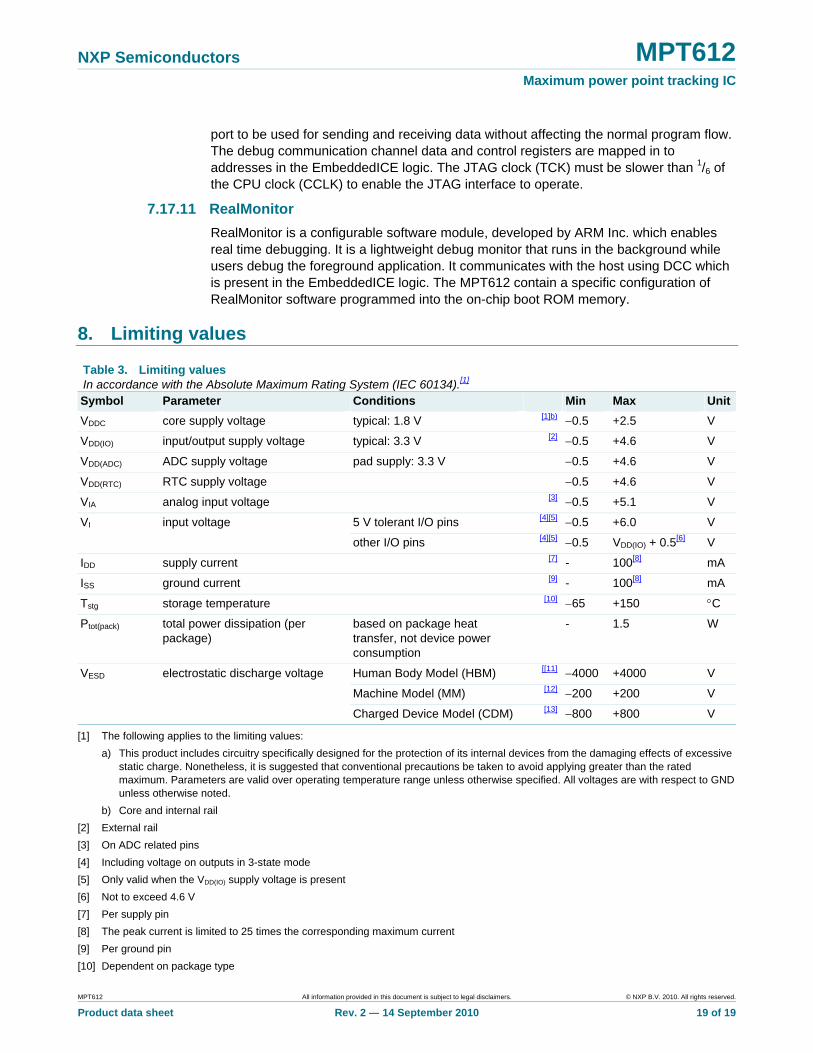
8. Limiting values
Table 3. Limiting values In accordance with the Absolute Maximum Rating System (IEC 60134).[1] Symbol Parameter Conditions Min Max UnitVDDC core supply voltage typical: 1.8 V [1]b)
−0.5 +2.5 V
VDD(IO) input/output supply voltage typical: 3.3 V [2] −0.5 +4.6 V
VDD(ADC) ADC supply voltage pad supply: 3.3 V −0.5 +4.6 V
VDD(RTC) RTC supply voltage −0.5 +4.6 V
VIA analog input voltage [3] −0.5 +5.1 V
VI input voltage 5 V tolerant I/O pins [4][5] −0.5 +6.0 V
other I/O pins [4][5] −0.5 VDD(IO) + 0.5[6]
V
IDD supply current [7] - 100[8]
mA
ISS ground current [9] - 100[8]
mA
Tstg storage temperature [10] −65 +150 °C
Ptot(pack) total power dissipation (per package)
based on package heat transfer, not device power consumption
- 1.5 W
VESD electrostatic discharge voltage Human Body Model (HBM) [[11] −4000 +4000 V
Machine Model (MM) [12] −200 +200 V
Charged Device Model (CDM) [13] −800 +800 V
[1] The following applies to the limiting values: a) This product includes circuitry specifically designed for the protection of its internal devices from the damaging effects of excessive
static charge. Nonetheless, it is suggested that conventional precautions be taken to avoid applying greater than the rated maximum. Parameters are valid over operating temperature range unless otherwise specified. All voltages are with respect to GND unless otherwise noted.
b) Core and internal rail [2] External rail [3] On ADC related pins [4] Including voltage on outputs in 3-state mode [5] Only valid when the VDD(IO) supply voltage is present [6] Not to exceed 4.6 V [7] Per supply pin [8] The peak current is limited to 25 times the corresponding maximum current [9] Per ground pin [10] Dependent on package type
NXP Semiconductors MPT612 Maximum power point tracking IC
MPT612 All information provided in this document is subject to legal disclaimers. © NXP B.V. 2010. All rights reserved.
Product data sheet Rev. 2 — 14 September 2010 20 of 20
[11] Performed per AEC-Q100-002 [12] Performed per AEC-Q100-003 [13] Performed per AEC-Q100-011
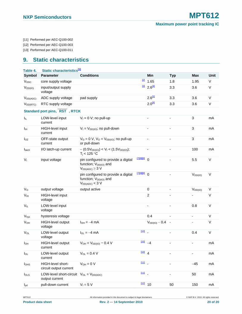
9. Static characteristics
Table 4. Static characteristics[1] Symbol Parameter Conditions Min Typ Max Unit VDDC core supply voltage [2]
1.65 1.8 1.95 V
VDD(IO) input/output supply voltage
[3] 2.6[4]
3.3 3.6 V
VDD(ADC) ADC supply voltage pad supply 2.6[5] 3.3 3.6 V
VDD(RTC) RTC supply voltage 2.0[6] 3.3 3.6 V
Standard port pins, RST , RTCK
IIL LOW-level input current
VI = 0 V; no pull-up - - 3 mA
IIH HIGH-level input current
VI = VDD(IO); no pull-down - - 3 mA
IOZ OFF-state output current
VO = 0 V, VO = VDD(IO); no pull-up or pull-down
- - 3 mA
Ilatch I/O latch-up current − (0.5VDD(IO)) < VI < (1.5VDD(IO)); Tj < 125 °C
- - 100 mA
VI input voltage pin configured to provide a digital function; VDD(IO) and VDD(ADC) ≥ 3 V
[7][8][9] 0 - 5.5 V
pin configured to provide a digital function; VDD(IO) and VDD(ADC) < 3 V
[7][8][9] 0 - VDD(IO) V
VO output voltage output active 0 - VDD(IO) V
VIH HIGH-level input voltage
2 - - V
VIL LOW-level input voltage
- - 0.8 V
Vhys hysteresis voltage 0.4 - - V
VOH HIGH-level output voltage
IOH = −4 mA VDD(IO) − 0.4 - - V
VOL LOW-level output voltage
IOL = −4 mA [10] - - 0.4 V
IOH HIGH-level output current
VOH = VDD(IO) − 0.4 V [10] −4 - - mA
IOL LOW-level output current
VOL = 0.4 V [10] 4 - - mA
IOHS HIGH-level short-circuit output current
VOH = 0 V [11] - - −45 mA
IOLS LOW-level short-circuit output current
VOL = VDD(ADC) [11] - - 50 mA
Ipd pull-down current VI = 5 V [12] 10 50 150 mA
NXP Semiconductors MPT612 Maximum power point tracking IC
MPT612 All information provided in this document is subject to legal disclaimers. © NXP B.V. 2010. All rights reserved.
Product data sheet Rev. 2 — 14 September 2010 21 of 21
Symbol Parameter Conditions Min Typ Max Unit Ipu pull-up current VI = 0 V [13]
−15 −50 −85 mA
VDD(IO) < VI < 5 V [12] 0 0 0 mA
IDDC core supply current Active mode; code while (1){} executed from flash; all peripherals enabled via PCONP register but not configured to run; CCLK = 70 MHz
VDDC = 1.8 V; Tamb = 25 °C - 41 70 mA
Power-down mode;
VDDC = 1.8 V; Tamb = 25 °C - 2.5 25 mA
VDDC = 1.8 V; Tamb = 85 °C - 35 105 mA
Deep power-down mode RTC off; SRAM off; Tamb = 25 °C
VDD(RTC) = 3.3 V; VDDC = 1.8 V - 0.7 - mA
IDD(RTC) RTC supply current Active mode CCLK = 70 MHz; PCLK = 12.5 MHz; PCLK enabled to RTCK; RTC clock = 32 kHz (from RTCX pins); Tamb = 25 °C
[14]
VDDC = 1.8 V; VDD(RTC) = 3.0 V - 10 15 mA
Power-down mode RTC clock = 32 kHz (from RTCX pins); Tamb = 25 °C
VDDC = 1.8 V; VDD(RTC) = 2.5 V - 7 12 mA
VDDC = 1.8 V; VDD(RTC) = 3.0 V - 8 12 mA
Deep power-down mode RTC off; SRAM off; Tamb = 25 °C
VDDC = 1.8 V; VDD(RTC) = 3.0 V - 8 - mA
I2C-bus pins VIH HIGH-level input
voltage 0.7 VDD(IO) - - V
VIL LOW-level input voltage
- - 0.3 VDD(IO)
V
Vhys hysteresis voltage - 0.5 VDD(IO) - V
VOL LOW-level output voltage
IOLS = 3 mA [10] - - 0.4 V
ILI input leakage current VI = VDD(IO) - 2 4 mA
VI = 5 V [15] - 10 22 mA
NXP Semiconductors MPT612 Maximum power point tracking IC
MPT612 All information provided in this document is subject to legal disclaimers. © NXP B.V. 2010. All rights reserved.
Product data sheet Rev. 2 — 14 September 2010 22 of 22
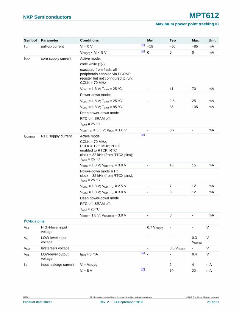
Symbol Parameter Conditions Min Typ Max Unit Oscillator pins Vi(XTAL1) input voltage on pin
XTAL1 0 - 1.8 V
Vo(XTAL2) output voltage on pin XTAL2
0 - 1.8 V
Vi(RTCX1) input voltage on pin RTCX1
0 - 1.8 V
Vo(RTCX2) output voltage on pin RTCX2
0 - 1.8 V
[1] Typical ratings are not guaranteed. The values listed are at room temperature (25 °C), nominal supply voltages. [2] Core and internal rail. [3] External rail. [4] If VDD(IO) < 3.0 V, the I/O pins are not 5 V tolerant and the ADC input voltage is limited to VDD(ADC) = 3.0 V. [5] If VDD(ADC) < 3.0 V, the I/O pins are not 5 V tolerant. [6] The RTC typically fails when VDD(RTC) drops below 1.6 V. [7] Including voltage on outputs in 3-state mode. [8] VDD(IO) supply voltages must be present. [9] 3-state outputs go into 3-state mode when VDD(IO) is grounded. [10] Accounts for 100 mV voltage drop in all supply lines. [11] Allowed as long as the current limit does not exceed the maximum current allowed by the device. [12] Minimum condition for VI = 4.5 V, maximum condition for VI = 5.5 V. VDD(ADC) ≥ 3.0 V and VDD(IO) ≥ 3.0 V. [13] Applies to PIO25:16. [14] Battery supply current on pin VDD(RTC). [15] Input leakage current to GND.
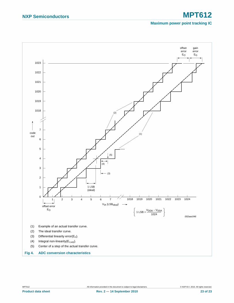
Table 5. ADC Static Characteristics VDD(ADC) = 2.5 V to 3.6 V; Tamb = -40 °C to +85 °C unless otherwise specified. ADC frequency 4.5 MHz Symbol Parameter Conditions Min Typ Max Unit VIA analog input voltage 0 - VDD(ADC) V
Cia analog input capacitance - - 1 pF
ED differential linearity error [1][2][3] - - ±1 LSB
EL(adj) integral non-linearity [1][2][4] - - ±2 LSB
EO offset error [1][5] - - ±3 LSB
EG gain error [1][6] - - ±0.5 %
ET absolute error [1][7] - - ±4 LSB
[1] Conditions: GNDADC = 0 V, VDD(ADC) = 3.3 V and VDD(IO) = 3.3 V for 10-bit resolution at full speed; VDD(ADC) = 2.6 V, VDD(IO) = 2.6 V for 8-bit resolution at full speed.
[2] The ADC is monotonic, there are no missing codes. [3] The differential linearity error (ED) is the difference between the actual step width and the ideal step width. See Fig 4. [4] The integral non-linearity (EL(adj)) is the peak difference between the center of the steps of the actual and the ideal transfer curve after
appropriate adjustment of gain and offset errors. See Fig 4. [5] The offset error (EO) is the absolute difference between the straight line which fits the actual curve and the straight line which fits the
ideal curve. See Fig 4. [6] The gain error (EG) is the relative difference in percent between the straight line fitting the actual transfer curve after removing offset
error and the straight line which fits the ideal transfer curve. See Fig 4. [7] The absolute error (ET) is the maximum difference between the center of the steps of the actual transfer curve of the non-calibrated
ADC and the ideal transfer curve. See Fig 4.
NXP Semiconductors MPT612 Maximum power point tracking IC
002aac046
1023
1022
1021
1020
1019
(2)
(1)
10241018 1019 1020 1021 1022 102371 2 3 4 5 6
7
6
5
4
3
2
1
0
1018
(5)
(4)
(3)
1 LSB(ideal)
codeout
VDDA − VSSA
1024
offset errorEO
gainerrorEG
offset errorEO
VIA (LSBideal)
1 LSB =
(1) Example of an actual transfer curve. (2) The ideal transfer curve. (3) Differential linearity error(ED). (4) Integral non-linearity(EL(adj)). (5) Center of a step of the actual transfer curve.
Fig 4. ADC conversion characteristics
MPT612 All information provided in this document is subject to legal disclaimers. © NXP B.V. 2010. All rights reserved.
Product data sheet Rev. 2 — 14 September 2010 23 of 23
NXP Semiconductors MPT612 Maximum power point tracking IC
MPT612 All information provided in this document is subject to legal disclaimers. © NXP B.V. 2010. All rights reserved.
Product data sheet Rev. 2 — 14 September 2010 24 of 24
10. Dynamic characteristics
Table 6. Dynamic characteristics Tamb = 0 °C to 70 °C for commercial applications, -40 °C to +85 °°C for industrial applications, VDDC, VDD(IO) over ranges[1] Symbol Parameter Conditions Min Typ[1][2]
Max Unit External clock fosc oscillator frequency
10 - 25 MHz
Tcy(clk) clock cycle time
40 - 100 ns
tCHCX clock HIGH time
Tcy(clk) × 0.4 - - ns
tCLCX clock LOW time
Tcy(clk) × 0.4 - - ns
tCLCH clock rise time - - 5 ns
tCHCL clock fall time - - 5 ns
Port pins (except PIO2 and PIO3) tr(o) output rise time - 10 - ns
tf(o) output fall time - 10 - ns
I2C-bus pins (PIO2 and PIO3) tf(o) output fall time VIH to VIL [1][2][3]
20 + 0.1 × Cb - - ns
[1] Parameters are valid over operating temperature range unless otherwise specified. [2] Typical ratings are not guaranteed. The values listed are at room temperature (25 °C), nominal supply voltages. [3] Bus capacitance Cb in pF, from 10 pF to 400 pF.
11. Application information
11.1 XTAL1 input The input voltage to the on-chip oscillators is limited to 1.8 V. When the oscillator is driven by a clock in slave mode, it is recommended that the input is coupled through a capacitor with Ci = 100 pF. To limit the input voltage to the specified range, an additional capacitor connected to ground (Cg), attenuates the input voltage by a factor Ci / (Ci + Cg). In slave mode, a minimum input voltage of 200 mV (RMS) is needed.
11.1.1 XTAL and RTC Printed Circuit Board (PCB) layout guidelines The crystal should be connected on the PCB as close as possible to the device’s oscillator input and output pins. The load capacitors Cx1 and Cx2 and Cx3, in case of third overtone crystal usage, must have a common ground plane. In addition, the external components must also be connected to the ground plain.
Any loops must be made as small as possible to keep the noise coupled and parasitics in via the PCB as small as possible. The values of Cx1 and Cx2 should be chosen smaller accordingly to the increase in parasitics of the PCB layout.
The MPT612 IC can be used with accompanying software only. The MPT612 software stack is designed to cater to different types of applications in the solar PV domain ranging from simple MPPT charge controller to advanced systems on street lighting applications to micro-inverters and DC-DC converters per panel.
NXP Semiconductors MPT612 Maximum power point tracking IC
12. MPT612 software overview The MPT612 IC can only be used with accompanying software. The MPT612 software stack is designed to meet the needs of different solar PV domain applications ranging from MPPT charge controllers to advanced street lighting system applications.
• Scalable software modules. Only those modules that are developed and tested are included in the final application image
• Implementation of the MPPT algorithm (patent pending) for generating maximum power from photovoltaic panel
• Easy to implement APIs for use with a range of peripherals ensure fast application programming
• Easy configuration for use with any PV panel • Easy configuration for use with any battery (up to 4 stage charging cycle) • Available for different IDE tools • Up to 15 kB of flash memory available for application software • Data logging capability through external memory • Complies with industry standard MISRA guidelines • Context-based API reference manual (included in the MPT612 user manual) • Distributed as libraries (object files) can be linked to application
MPT612 All information provided in this document is subject to legal disclaimers. © NXP B.V. 2010. All rights reserved.
Product data sheet Rev. 2 — 14 September 2010 25 of 25
NXP Semiconductors MPT612 Maximum power point tracking IC
12.1 Architecture
brb513
SAMPLE CHARGE CONTROLLER AND LOAD-CONTROL APPLICATION
SAFTEYCHECK
STATUSINDICATION
BUCKBOOST
CHANGE
DATALOG
LEAD-ACID BATTERY CHARGING MODULE
CHARGECYCLE
IMPLEMENT
BATTCONFIG
BATTDATA LOG
MPPTCore
HARDWARE FUNCTIONAL ABSTRACTION LAYER (HFAL)
MPT612 ICSYSTEM HARDWARE
SAMPLE APPLICATION 2
SAMPLE APPLICATION 1
MPT612 IC + SW
MPPTRACKINGMODULE
MPPT CORCONFIG
MPPTSAFTEYCHECK
Fig 5. MPT612SW Architecture
12.2 MPT612 software modules This module consists of two sub modules: Hardware Functional Abstraction Layer (HFAL) and MPPTCore. Both these sub modules are delivered as software libraries together with the MPT612 IC. It is mandatory to use these modules to access the MPT612’s MPPT functionality.
12.2.1 Hardware Functional Abstraction Layer (HFAL) This module contains the functional abstraction of different peripherals that are of interest to the application layer as well as different modules of MPT612 software. This layer contains mini kernel functionality such as implementations of a round-robin scheduler, task creation and software timers. These functions are useful during development of applications based on the MPT612.
A range of different peripherals used in the application, such as PWM, Interrupts, software timers, GPIO, UART and Flash can be accessed using this module. In addition, utilities for logging the data onto the flash and printing the messages onto the console screen are accessed from this layer.
MPT612 All information provided in this document is subject to legal disclaimers. © NXP B.V. 2010. All rights reserved.
Product data sheet Rev. 2 — 14 September 2010 26 of 26
NXP Semiconductors MPT612 Maximum power point tracking IC
12.2.2 MPPTCore module This module contains the Maximum PowerPoint Tracking (MPPT) algorithm. This algorithm continuously tracks the maximum power point of the PV panel and makes the system to operate at the MPP which ensures the maximum power is generated from the PV. This module supports the well documented APIs that aid in application programming. Typical module functionality includes, starting the MPP tracking algorithm, enabling/disabling the MPP tracking algorithm and retrieving logged parameters from the MPPTCore module.
12.3 Lead-Acid battery charging module This is an optional software library provided along with the MPT612 IC. This module implements the lead-acid battery charge cycle for 2-stage, 3-stage and 4-stage batteries. Using the easy configuration for the battery parameters and well documented APIs, the user can design an application with ease. This module together with the MPT612SW will help in the creation of power management systems for battery charging for home and street lighting applications.
12.4 Sample charge controller and load control application This module implements the sample charge controller and load control application for the specification of the MPT612 reference board. It uses features of the MPT612SW and lead-acid battery charging module to implement a typical charge controller application.
12.5 Sample applications Using MPT612SW and lead-acid battery charging module, solutions for several applications can be generated such as:
• dusk-to-dawn lighting applications • street lighting applications • traffic lighting applications • solar based mobile chargers • DC-DC converters in panels • micro inverters.
In the SW architecture diagram shown in Fig 5, SampleApplication1 will interact directly with MPPTCore module to extract the maximum power which can use a micro-inverter, to feed it to the grid. SampleApplication2 utilizes the services of the battery charging algorithm to charge the battery and can be used to control different lighting applications.
MPT612 All information provided in this document is subject to legal disclaimers. © NXP B.V. 2010. All rights reserved.
Product data sheet Rev. 2 — 14 September 2010 27 of 27
NXP Semiconductors MPT612 Maximum power point tracking IC
13. MPT612SW interfaces
13.1 Hardware Functional Abstraction Layer interfaces
Table 7. HFAL Interfaces Interface Description nxLibMpt_Hfal_Irq_InstallHandler installs the interrupt handler for the IRQ mentioned
nxLibMpt_Hfal_Irq_FreeHandler frees the interrupt handler installed using nxLibMpt_Hfal_Irq_InstallHandler
nxLibMpt_Hfal_Irq_Enable enables the interrupt associated with an IRQ
nxLibMpt_Hfal_Irq_Disable disables the interrupt associated with an IRQ
nxLibMpt_Hfal_Irq_SetPriority sets the priority of the interrupt associated with an IRQ
nxLibMpt_Hfal_Irq_GetPriority reads the priority of the interrupt associated with an IRQ
nxLibMpt_Hfal_Irq_SaveFlags saves the current interrupt enable state and disables the interrupts
nxLibMpt_Hfal_Irq_RestoreFlags restores the previous interrupt state (enable/disable)
nxLibMpt_Hfal_Schedular_RestoreFlags restores the previous scheduler state (enable/disable)
nxLibMpt_Hfal_Schedular_SaveFlags saves the current scheduler state and then disables the scheduler
nxLibMpt_Hfal_Task_Create creates a task with given round-robin time slice in ticks
nxLibMpt_Hfal_Timer_Create creates a software timer and returns the timer ID
nxLibMpt_Hfal_Timer_Delete deletes the created software timer
nxLibMpt_Hfal_Timer_CheckTimeOut checks if the software timer is running and triggers it, when necessary
nxLibMpt_Hfal_Timer_Start starts the software timer
nxLibMpt_Hfal_Timer_Stop stops the software timer
nxLibMpt_Hfal_Timer_Delay delays the execution till the specified timeout elapses
nxLibMpt_Hfal_Timer_SetTimeOut sets the timeout value for the software timer
nxLibMpt_Hfal_Timer_GetTimeOut reads the current timeout value of the software timer
nxLibMpt_Hfal_Pwm_Init initializes the PWM unit
nxLibMpt_Hfal_Pwm_SetDutyCycle sets the duty cycle of the PWM pin
nxLibMpt_Hfal_Pwm_GetDutyCycle reads the current duty cycle of the PWM pin
nxLibMpt_Hfal_Pwm_SetCount sets the duty cycle count of the specified PWM pin
nxLibMpt_Hfal_Pwm_GetCount reads the current duty cycle count of the specified PWM pin
nxLibMpt_Hfal_Gpio_Init initializes the GPIO pin direction (input/output)
nxLibMpt_Hfal_Gpio_SetValue sets the value of the GPIO pin to the entered value
nxLibMpt_Hfal_Gpio_GetValue reads the current value of the GPIO pin
nxLibMpt_Hfal_Flash_Erase erases the flash blocks
nxLibMpt_Hfal_Flash_Read reads the data from the specified flash address
nxLibMpt_Hfal_Flash_Write data is written to the specified flash address
nxLibMpt_Hfal_DataLog_Init initializes the data logging module
nxLibMpt_Hfal_DataLog_ReadData_Latest reads the recent data that is logged
nxLibMpt_Hfal_DataLog_WriteData writes the log data to the flash
nxLibMpt_Hfal_Adc_ReadCounts reads the ADC channel and returns the counts corresponding to the incoming signal
nxLibMpt_Hfal_Uart_Init initializes the console UART port at the specified frequency
nxLibMpt_Hfal_Uart_WriteByte writes a byte to the UART console
MPT612 All information provided in this document is subject to legal disclaimers. © NXP B.V. 2010. All rights reserved.
Product data sheet Rev. 2 — 14 September 2010 28 of 28

NXP Semiconductors MPT612 Maximum power point tracking IC
MPT612 All information provided in this document is subject to legal disclaimers. © NXP B.V. 2010. All rights reserved.
Product data sheet Rev. 2 — 14 September 2010 29 of 29
Interface Description nxLibMpt_Hfal_Uart_ReadByte reads a byte from the UART console
nxLibMpt_Hfal_Uart_IsKeyPressed returns key down status to the UART console
nxLibMpt_Hfal_Uart_FlushFifo flushes the UART console port FIFO
nxLibMpt_Hfal_Util_Puts writes a string to the UART console port
nxLibMpt_Hfal_Util_Gets reads a string from the UART console port
nxLibMpt_Hfal_Util_PrintNum prints a number on the UART console port in decimals
nxLibMpt_Hfal_Util_Atoi converts from string to integer number
nxLibMpt_Hfal_Util_Memcpy copies the memory contents from one buffer to another
nxLibMpt_Hfal_Util_Memset fills the memory locations with the pattern provided
nxLibMpt_Hfal_Util_Memcmp returns the comparison of two specified buffers
nxLibMpt_Hfal_Util_IsKeyPressed returns key down status on the UART port
nxLibMpt_Hfal_Util_Flush flushes all the data present in the UART port buffer
nxLibMpt_Hfal_Led_Init initializes the LED module
nxLibMpt_Hfal_Led_Blink_Enable enables the blinking of the specified LED
nxLibMpt_Hfal_Led_Blink_Disable disables the blinking of the specified LED
nxLibMpt_Hfal_SysParams_IsParamValid returns the status of the specified parameter consistently has a longer duration than the reference provided
13.2 MPPTCore module interfaces
Table 8. MPPTCore Interfaces Interface Description nxLibMpt_MpptCore_Init initializes the MPPTCore module with the PV panel configuration
parameters
nxLibMpt_MpptCore_SetParams sets the required parameters in MPPTCore module
nxLibMpt_MpptCore_GetParams reads the current MPPTCore module parameters
nxLibMpt_MpptCore_GetLogParams reads the logged parameters from MPPTCore module
nxLibMpt_MpptCore_Start starts the MPP tracking algorithm
nxLibMpt_MpptCore_Enable enables the previously disabled MPP tracking algorithm
nxLibMpt_MpptCore_Disable disables the MPP tracking algorithm
nxLibMpt_MpptCore_IsEnabled returns the status of MPP tracking algorithm (enabled or disabled)
nxLibMpt_MpptCore_GetStatus reads the current status of the MPPTCore module
NXP Semiconductors MPT612 Maximum power point tracking IC
13.3 Lead-acid battery charging module interfaces
Table 9. MPPTCore Interfaces Interface Description nxLibMpt_Batla_Init initializes the lead-acid battery charging module with the battery
configuration parameters
nxLibMpt_Batla_SetParams sets the parameters required in lead-acid battery charging module
nxLibMpt_Batla_GetParams reads the current parameters stored in lead-acid battery charging module
nxLibMpt_Batla_GetLogParams reads the logged parameters in lead-acid battery charging module
nxLibMpt_Batla_Start starts the lead-acid battery charging algorithm
nxLibMpt_Batla_Enable enables the lead-acid battery charging algorithm
nxLibMpt_Batla_Disable disables the lead-acid battery charging algorithm
nxLibMpt_Batla_IsEnabled returns the status of lead-acid battery charging algorithm enabled or disabled
nxLibMpt_Batla_GetStatus reads the status of the lead-acid battery charging module
13.4 Interfaces to be implemented by application
Table 10. MPPTCore Interfaces Interface Description nxLibMpt_Hfal_SysParams_Init called during system initialization. Typically this API should be
implemented to store any initialized system parameters data
nxLibMpt_Hfal_SysParams_ReadPVParams returns the PV voltage and current values
nxLibMpt_Hfal_SysParams_ReadBatVoltage returns the lead-acid battery voltage
nxLibMpt_Hfal_SysParams_ReadBatCurrent returns the lead-acid battery current
nxLibMpt_Hfal_SysParams_ReadLoadCurrent returns the load current
nxLibMpt_Hfal_SysParams_ReadBatTemperature returns the battery temperature
nxLibMpt_Hfal_SysParams_GetPVOpenCkt_Voltage returns the PV open circuit voltage
nxLibMpt_Hfal_SysParams_BringPVVG_ToNewLevel sets the PV voltage to a new voltage specified
nxLibMpt_Hfal_SysParams_SwitchLED_ON switches on the specified LED
nxLibMpt_Hfal_SysParams_SwitchLED_OFF switches off the specified LED
MPT612 All information provided in this document is subject to legal disclaimers. © NXP B.V. 2010. All rights reserved.
Product data sheet Rev. 2 — 14 September 2010 30 of 30

NXP Semiconductors MPT612 Maximum power point tracking IC
14. Package outline
UNITA
max. A1 A2 A3 bp c E(1) e HE L Lp Zywv θ
REFERENCESOUTLINEVERSION
EUROPEANPROJECTION ISSUE DATE
IEC JEDEC JEITA
mm 1.6 0.200.05
1.451.35
0.250.270.17
0.180.12
7.16.9 0.5
9.158.85
0.950.55
70
o
o0.12 0.10.21
DIMENSIONS (mm are the original dimensions)
Note
1. Plastic or metal protrusions of 0.25 mm maximum per side are not included.
0.750.45
SOT313-2 MS-026136E0500-01-1903-02-25
D(1) (1)(1)
7.16.9
HD
9.158.85
EZ
0.950.55
D
bp
e
E
B
12
DH
bp
EH
v M B
D
ZD
A
ZE
e
v M A
1
48
37
36 25
24
13
θ
A1A
Lp
detail X
L
(A )3A2
X
y
c
w M
w M
0 2.5 5 mm
scale
pin 1 index
LQFP48: plastic low profile quad flat package; 48 leads; body 7 x 7 x 1.4 mm SOT313-2
Fig 6. Package outline
MPT612 All information provided in this document is subject to legal disclaimers. © NXP B.V. 2010. All rights reserved.
Product data sheet Rev. 2 — 14 September 2010 31 of 31
NXP Semiconductors MPT612 Maximum power point tracking IC
MPT612 All information provided in this document is subject to legal disclaimers. © NXP B.V. 2010. All rights reserved.
Product data sheet Rev. 2 — 14 September 2010 32 of 32
15. Abbreviations
Table 11. Abbreviations Acronym Description ADC Analog-to-Digital Converter
AMBA Advanced Microcontroller Bus Architecture
APB Advanced Peripheral Bus
DCC Debug Communications Channel
DSP Digital Signal Processor
FIFO First In, First Out
FIQ Fast Interrupt reQuest
GPIO General Purpose Input/Output
IAP In-Application Programming
IRQ Interrupt Request
ISP In-System Programming
MPPT Maximum Power Point Tracking
PIO Programmable Input Output
PLL Phase-Locked Loop
PV PhotoVoltaic
PWM Pulse-Width Modulator
SPI Serial Peripheral Interface
SRAM Static Random Access Memory
SSI Synchronous Serial Interface
SSP Synchronous Serial Port
TTL Transistor-Transistor Logic
UART Universal Asynchronous Receiver/Transmitter
VIC Vectored Interrupt Controller
16. Revision history
Table 12. Revision history Document ID Release date Data sheet status Change notice Supersedes MPT612 v.2 20100914 Product data sheet - MPT612 v.1
Modifications: • Data sheet status changed from Objective data sheet to Product data sheet. MPT612 v.1 20100615 Objective data sheet - -
NXP Semiconductors MPT612 Maximum power point tracking IC
MPT612 All information provided in this document is subject to legal disclaimers. © NXP B.V. 2010. All rights reserved.
Product data sheet Rev. 2 — 14 September 2010 33 of 33
17. Legal information
17.1 Data sheet status Document status[1][2]
Product status[3] Definition
Objective [short] data sheet Development This document contains data from the objective specification for product development. Preliminary [short] data sheet Qualification This document contains data from the preliminary specification. Product [short] data sheet Production This document contains the product specification.
[1] Please consult the most recently issued document before initiating or completing a design.
[2] The term ‘short data sheet’ is explained in section “Definitions”.
[3] The product status of device(s) described in this document may have changed since this document was published and may differ in case of multiple devices. The latest product status information is available on the Internet at URL http://www.nxp.com.
17.2 Definitions Draft — The document is a draft version only. The content is still under internal review and subject to formal approval, which may result in modifications or additions. NXP Semiconductors does not give any representations or warranties as to the accuracy or completeness of information included herein and shall have no liability for the consequences of use of such information.
Short data sheet — A short data sheet is an extract from a full data sheet with the same product type number(s) and title. A short data sheet is intended for quick reference only and should not be relied upon to contain detailed and full information. For detailed and full information see the relevant full data sheet, which is available on request via the local NXP Semiconductors sales office. In case of any inconsistency or conflict with the short data sheet, the full data sheet shall prevail.
Product specification — The information and data provided in a Product data sheet shall define the specification of the product as agreed between NXP Semiconductors and its customer, unless NXP Semiconductors and customer have explicitly agreed otherwise in writing. In no event however, shall an agreement be valid in which the NXP Semiconductors product is deemed to offer functions and qualities beyond those described in the Product data sheet.
17.3 Disclaimers Limited warranty and liability — Information in this document is believed to be accurate and reliable. However, NXP Semiconductors does not give any representations or warranties, expressed or implied, as to the accuracy or completeness of such information and shall have no liability for the consequences of use of such information.
In no event shall NXP Semiconductors be liable for any indirect, incidental, punitive, special or consequential damages (including - without limitation - lost profits, lost savings, business interruption, costs related to the removal or replacement of any products or rework charges) whether or not such damages are based on tort (including negligence), warranty, breach of contract or any other legal theory.
Notwithstanding any damages that customer might incur for any reason whatsoever, NXP Semiconductors’ aggregate and cumulative liability towards customer for the products described herein shall be limited in accordance with the Terms and conditions of commercial sale of NXP Semiconductors.
Right to make changes — NXP Semiconductors reserves the right to make changes to information published in this document, including without limitation specifications and product descriptions, at any time and without notice. This document supersedes and replaces all information supplied prior to the publication hereof.
Suitability for use — NXP Semiconductors products are not designed, authorized or warranted to be suitable for use in life support, life-critical or safety-critical systems or equipment, nor in applications where failure or malfunction of an NXP Semiconductors product can reasonably be expected to result in personal injury, death or severe property or environmental
damage. NXP Semiconductors accepts no liability for inclusion and/or use of NXP Semiconductors products in such equipment or applications and therefore such inclusion and/or use is at the customer’s own risk.
Applications — Applications that are described herein for any of these products are for illustrative purposes only. NXP Semiconductors makes no representation or warranty that such applications will be suitable for the specified use without further testing or modification.
Customers are responsible for the design and operation of their applications and products using NXP Semiconductors products, and NXP Semiconductors accepts no liability for any assistance with applications or customer product design. It is customer’s sole responsibility to determine whether the NXP Semiconductors product is suitable and fit for the customer’s applications and products planned, as well as for the planned application and use of customer’s third party customer(s). Customers should provide appropriate design and operating safeguards to minimize the risks associated with their applications and products.
NXP Semiconductors does not accept any liability related to any default, damage, costs or problem which is based on any weakness or default in the customer’s applications or products, or the application or use by customer’s third party customer(s). Customer is responsible for doing all necessary testing for the customer’s applications and products using NXP Semiconductors products in order to avoid a default of the applications and the products or of the application or use by customer’s third party customer(s). NXP does not accept any liability in this respect.
Limiting values — Stress above one or more limiting values (as defined in the Absolute Maximum Ratings System of IEC 60134) will cause permanent damage to the device. Limiting values are stress ratings only and (proper) operation of the device at these or any other conditions above those given in the Recommended operating conditions section (if present) or the Characteristics sections of this document is not warranted. Constant or repeated exposure to limiting values will permanently and irreversibly affect the quality and reliability of the device.
Terms and conditions of commercial sale — NXP Semiconductors products are sold subject to the general terms and conditions of commercial sale, as published at http://www.nxp.com/profile/terms, unless otherwise agreed in a valid written individual agreement. In case an individual agreement is concluded only the terms and conditions of the respective agreement shall apply. NXP Semiconductors hereby expressly objects to applying the customer’s general terms and conditions with regard to the purchase of NXP Semiconductors products by customer.
No offer to sell or license — Nothing in this document may be interpreted or construed as an offer to sell products that is open for acceptance or the grant, conveyance or implication of any license under any copyrights, patents or other industrial or intellectual property rights.
Export control — This document as well as the item(s) described herein may be subject to export control regulations. Export might require a prior authorization from national authorities.
Non-automotive qualified products — Unless this data sheet expressly states that this specific NXP Semiconductors product is automotive qualified, the product is not suitable for automotive use. It is neither qualified nor tested in accordance with automotive testing or application requirements.

NXP Semiconductors MPT612 Maximum power point tracking IC
MPT612 All information provided in this document is subject to legal disclaimers. © NXP B.V. 2010. All rights reserved.
Product data sheet Rev. 2 — 14 September 2010 34 of 34
NXP Semiconductors accepts no liability for inclusion and/or use of non-automotive qualified products in automotive equipment or applications.
In the event that customer uses the product for design-in and use in automotive applications to automotive specifications and standards, customer (a) shall use the product without NXP Semiconductors’ warranty of the product for such automotive applications, use and specifications, and (b) whenever customer uses the product for automotive applications beyond NXP Semiconductors’ specifications such use shall be solely at customer’s own risk, and (c) customer fully indemnifies NXP Semiconductors for any liability, damages or failed product claims resulting from customer design and use of the product for automotive applications beyond NXP Semiconductors’ standard warranty and NXP Semiconductors’ product specifications.
17.4
Trademarks Notice: All referenced brands, product names, service names and trademarks are property of their respective owners.
I2C-bus — is a trademark of NXP B.V.
18. Contact information For sales office addresses, please send an email to: [email protected] For additional information, please visit: http://www.nxp.com
NXP Semiconductors MPT612 Maximum power point tracking IC
19. List of figures
Fig 1. Block diagram ................................................... 3 Fig 2. Pin Configuration .............................................. 4 Fig 3. System Memory Map ...................................... 10 Fig 4. ADC conversion characteristics ...................... 23 Fig 5. MPT612SW Architecture ................................. 26 Fig 6. Package outline .............................................. 31
MPT612 All information provided in this document is subject to legal disclaimers. © NXP B.V. 2010. All rights reserved.
Product data sheet Rev. 2 — 14 September 2010 35 of 35

NXP Semiconductors MPT612 Maximum power point tracking IC
20. List of tables
Table 1. Ordering information ......................................... 3 Table 2. Pin description .................................................. 5 Table 3. Limiting values ................................................ 19 Table 4. Static characteristics[1] .................................... 20 Table 5. ADC Static Characteristics .............................. 22 Table 6. Dynamic characteristics .................................. 24 Table 7. HFAL Interfaces .............................................. 28 Table 8. MPPTCore Interfaces ..................................... 29 Table 9. MPPTCore Interfaces ..................................... 30 Table 10. MPPTCore Interfaces ..................................... 30 Table 11. Abbreviations .................................................. 32 Table 12. Revision history ............................................... 32
MPT612 All information provided in this document is subject to legal disclaimers. © NXP B.V. 2010. All rights reserved.
Product data sheet Rev. 2 — 14 September 2010 36 of 36

NXP Semiconductors MPT612 Maximum power point tracking IC
Please be aware that important notices concerning this document and the product(s) described herein, have been included in the section 'Legal information'.
© NXP B.V. 2010. All rights reserved.
For more information, please visit: http://www.nxp.com For sales office addresses, please send an email to: [email protected]
Date of release: 14 September 2010Document identifier: MPT612
21. Contents
1. General description ............................................. 1 2. Features and benefits ......................................... 2 3. Applications ......................................................... 2 4. Ordering information .......................................... 3 5. Block diagram ...................................................... 3 6. Pinning information ............................................ 4 6.1 Pinning ............................................................... 4 6.2 Pin description .................................................... 5 7. Functional description ........................................ 9 7.1 Architectural overview ........................................ 9 7.2 On-chip flash program memory .......................... 9 7.3 On-chip static RAM ............................................ 9 7.4 Memory map .................................................... 10 7.5 Interrupt controller ............................................ 10 7.5.1 Interrupt sources .............................................. 11 7.6 Pin connect block ............................................. 11 7.7 Fast general purpose parallel I/O ..................... 11 7.8 10-bit ADC ........................................................ 12 7.9 UARTs.............................................................. 12 7.10 I2C-bus serial I/O controllers ............................ 12 7.11 SPI serial I/O controller .................................... 13 7.12 SSP serial I/O controller ................................... 13 7.13 General purpose 32-bit timers/external event
counters ........................................................... 13 7.14 General purpose 16-bit timers/external event
counters ........................................................... 14 7.15 Watchdog timer ................................................ 15 7.16 Real-time clock ................................................. 15 7.17 System control ................................................. 15 7.17.1 Crystal oscillator ............................................... 15 7.17.2 PLL ................................................................... 15 7.17.3 Reset and wake-up timer ................................. 16 7.17.3.1 Wake-up timer description ................................ 16 7.17.4 Code security (Code Read Protection) ............. 17 7.17.5 External interrupt inputs ................................... 17 7.17.6 Memory mapping control .................................. 17 7.17.7 Power control ................................................... 17 7.17.8 APB .................................................................. 18 7.17.9 Emulation and debugging ................................ 18 7.17.10 EmbeddedICE .................................................. 18 7.17.11 RealMonitor ...................................................... 19 8. Limiting values .................................................. 19 9. Static characteristics ........................................ 20 10. Dynamic characteristics ................................... 24 11. Application information .................................... 24
11.1 XTAL1 input ...................................................... 24 11.1.1 XTAL and RTC Printed Circuit Board (PCB)
layout guidelines ............................................... 24 12. MPT612 software overview ............................... 25 12.1 Architecture ...................................................... 26 12.2 MPT612 software modules ............................... 26 12.2.1 Hardware Functional Abstraction Layer (HFAL)
......................................................................... 26 12.2.2 MPPTCore module ........................................... 27 12.3 Lead-Acid battery charging module .................. 27 12.4 Sample charge controller and load control
application ........................................................ 27 12.5 Sample applications ......................................... 27 13. MPT612SW interfaces ....................................... 28 13.1 Hardware Functional Abstraction Layer
interfaces .......................................................... 28 13.2 MPPTCore module interfaces .......................... 29 13.3 Lead-acid battery charging module interfaces .. 30 13.4 Interfaces to be implemented by application .... 30 14. Package outline ................................................. 31 15. Abbreviations ..................................................... 32 16. Revision history ................................................. 32 17. Legal information .............................................. 33 17.1 Data sheet status ............................................. 33 17.2 Definitions ......................................................... 33 17.3 Disclaimers ....................................................... 33 17.4 Trademarks ...................................................... 34 18. Contact information .......................................... 34 19. List of figures ..................................................... 35 20. List of tables ...................................................... 36 21. Contents ............................................................. 37