mpc5516 data sheet - digi-keymedia.digikey.com/pdf/data sheets/freescale semi/mpc5607b.pdf• boot...
TRANSCRIPT

Freescale SemiconductorData Sheet: Advance Information
Document Number: MPC5607BRev. 3, 01/2010
© Freescale Semiconductor, Inc., 2010. All rights reserved.
Preliminary—Subject to Change Without Notice
This document contains information on a product under development. Freescale reserves the right to change or discontinue this product without notice.
MPC5607B
176LQFP (24 x 24) 144 LQFP (20 x 20 ) 100 LQFP (14 x 14 )208 MAPBGA (17 x 17 )
Features• Single issue, 32-bit CPU core complex (e200z0h)
— Compliant with the Power Architecture™ embedded category
— Enhanced instruction set allowing variable length encoding (VLE) for code size footprint reduction. With the optional encoding of mixed 16-bit and 32-bit instructions, it is possible to achieve significant code size footprint reduction.
• Up to 1.5 Mbytes on-chip Flash supported with the Flash controller
• Up to 96 Kbytes on-chip SRAM• Memory protection unit (MPU) with 8 region
descriptors and 32-byte region granularity on certain family members
• Interrupt controller (INTC) capable of handling 204 selectable-priority interrupt sources
• Frequency modulated phase-locked loop (FMPLL)• Crossbar switch architecture for concurrent access to
peripherals, Flash, or RAM from multiple bus masters
• 16-channel eDMA controller with multiple transfer request sources using DMA multiplexer
• Boot assist module (BAM) supports internal Flash programming via a serial link (CAN or SCI)
• Timer supports I/O channels providing a range of 16-bit input capture, output compare, and pulse width modulation functions (eMIOS)
• 2 analog-to-digital converters (ADC): one 10-bit and one 12-bit
• Cross Trigger Unit to enable synchronization of ADC conversions with a timer event from the eMIOS or PIT
• Up to 6 serial peripheral interface (DSPI) modules• Up to 10 serial communication interface (LINFlex)
modules• Up to 6 enhanced full CAN (FlexCAN) modules
with configurable buffers • 1 inter-integrated circuit (I2C) interface module• Up to 149 configurable general purpose pins
supporting input and output operations (package dependent)
• Real-Time Counter (RTC)— Clock source from internal 128 kHz or 16 MHz
oscillator supporting autonomous wakeup with 1 ms resolution with maximum timeout of 2 seconds
— Optional support for RTC with clock source from external 32 kHz crystal oscillator, supporting wakeup with 1 sec resolution and maximum timeout of 1 hour
• Up to 8 periodic interrupt timers (PIT) with 32-bit counter resolution
• Nexus development interface (NDI) per IEEE-ISTO 5001-2003 Class Two Plus
• Device/board boundary scan testing supported per Joint Test Action Group (JTAG) of IEEE (IEEE 1149.1)
• On-chip voltage regulator (VREG) for regulation of input supply for all internal levels
MPC5607B Microcontroller Data Sheet
Bec
ause
of a
n or
der f
rom
the
Uni
ted
Sta
tes
Inte
rnat
iona
l Tra
de C
omm
issi
on, B
GA
-pac
kage
d pr
oduc
t lin
es a
nd p
art n
umbe
rs in
dica
ted
here
cur
rent
ly a
re
not a
vaila
ble
from
Fre
esca
le fo
r im
port
or s
ale
in th
e U
nite
d S
tate
s pr
ior t
o S
epte
mbe
r 201
0: M
PC
560x
B p
rodu
cts
in 2
08 M
AP
BG
A p
acka
ges

MPC5607B Microcontroller Data Sheet, Rev. 3
Preliminary—Subject to Change Without NoticeFreescale Semiconductor2
Table of Contents1 General description. . . . . . . . . . . . . . . . . . . . . . . . . . . . . . . . . .3
1.1 Block diagram . . . . . . . . . . . . . . . . . . . . . . . . . . . . . . . . .42 Package pinouts . . . . . . . . . . . . . . . . . . . . . . . . . . . . . . . . . . . .7
2.1 176LQFP pin configuration . . . . . . . . . . . . . . . . . . . . . . .82.2 144LQFP pin configuration . . . . . . . . . . . . . . . . . . . . . . .92.3 208MAPBGA pin configuration . . . . . . . . . . . . . . . . . . .10
3 Electrical characteristics . . . . . . . . . . . . . . . . . . . . . . . . . . . . .113.1 Parameter classification . . . . . . . . . . . . . . . . . . . . . . . .113.2 NVUSRO register . . . . . . . . . . . . . . . . . . . . . . . . . . . . .11
3.2.1 NVUSRO[PAD3V5V] field description . . . . . . . .113.2.2 NVUSRO[OSCILLATOR_MARGIN] field description. . . . . . . . . . . . . . . . . . . . . . . . . . . . . . . . . . .123.2.3 NVUSRO[WATCHDOG_EN] field description . .12
3.3 Absolute maximum ratings . . . . . . . . . . . . . . . . . . . . . .133.4 Recommended operating conditions . . . . . . . . . . . . . .143.5 Thermal characteristics. . . . . . . . . . . . . . . . . . . . . . . . .17
3.5.1 External ballast resistor recommendations . . . .173.5.2 Package thermal characteristics . . . . . . . . . . . .173.5.3 Power considerations. . . . . . . . . . . . . . . . . . . . .18
3.6 I/O pad electrical characteristics . . . . . . . . . . . . . . . . . .183.6.1 I/O pad types . . . . . . . . . . . . . . . . . . . . . . . . . . .183.6.2 I/O input DC characteristics. . . . . . . . . . . . . . . .193.6.3 I/O output DC characteristics. . . . . . . . . . . . . . .213.6.4 Output pin transition times. . . . . . . . . . . . . . . . .233.6.5 I/O pad current specification . . . . . . . . . . . . . . .24
3.7 nRSTIN electrical characteristics . . . . . . . . . . . . . . . . .273.8 Power management electrical characteristics. . . . . . . .30
3.8.1 Voltage regulator electrical characteristics . . . .303.8.2 Voltage monitor electrical characteristics. . . . . .33
3.9 Low voltage domain power consumption . . . . . . . . . . .353.10 Flash memory electrical characteristics . . . . . . . . . . . .37
3.10.1 Program/Erase characteristics. . . . . . . . . . . . . .373.10.2 Flash power supply DC characteristics . . . . . . .38
3.10.3 Start-up/Switch-off timings . . . . . . . . . . . . . . . . 403.11 Electromagnetic compatibility (EMC) characteristics. . 40
3.11.1 Designing hardened software to avoid noise problems . . . . . . . . . . . . . . . . . . . . . . . . . . . . . . 403.11.2 Electromagnetic interference (EMI) . . . . . . . . . 413.11.3 Absolute maximum ratings (electrical sensitivity)41
3.12 Fast external crystal oscillator (4 to 16 MHz)electrical characteristics . . . . . . . . . . . . . . . . . . . . . . . . . . . . 423.13 Slow external crystal oscillator (32 kHz) electrical characteristics . . . . . . . . . . . . . . . . . . . . . . . . . . . . 453.14 FMPLL electrical characteristics . . . . . . . . . . . . . . . . . 483.15 Fast internal RC oscillator (16 MHz)electrical characteristics . . . . . . . . . . . . . . . . . . . . . . . . . . . . 483.16 Slow internal RC oscillator (128 kHz)electrical characteristics . . . . . . . . . . . . . . . . . . . . . . . . . . . . 493.17 ADC electrical characteristics . . . . . . . . . . . . . . . . . . . 50
3.17.1 Introduction . . . . . . . . . . . . . . . . . . . . . . . . . . . 503.17.2 Input impedance and ADC accuracy . . . . . . . . 513.17.3 ADC electrical characteristics . . . . . . . . . . . . . 56
3.18 On-chip peripherals . . . . . . . . . . . . . . . . . . . . . . . . . . . 643.18.1 Current consumption . . . . . . . . . . . . . . . . . . . . 643.18.2 DSPI characteristics. . . . . . . . . . . . . . . . . . . . . 663.18.3 Nexus characteristics . . . . . . . . . . . . . . . . . . . . 733.18.4 JTAG characteristics. . . . . . . . . . . . . . . . . . . . . 74
4 Package characteristics. . . . . . . . . . . . . . . . . . . . . . . . . . . . . 754.1 Package mechanical data . . . . . . . . . . . . . . . . . . . . . . 75
4.1.1 176 LQFP. . . . . . . . . . . . . . . . . . . . . . . . . . . . . 754.1.2 144 LQFP. . . . . . . . . . . . . . . . . . . . . . . . . . . . . 794.1.3 100 LQFP. . . . . . . . . . . . . . . . . . . . . . . . . . . . . 824.1.4 208MAPBGA . . . . . . . . . . . . . . . . . . . . . . . . . . 86
5 Ordering information . . . . . . . . . . . . . . . . . . . . . . . . . . . . . . . 896 Revision history . . . . . . . . . . . . . . . . . . . . . . . . . . . . . . . . . . . 90
Bec
ause
of a
n or
der f
rom
the
Uni
ted
Sta
tes
Inte
rnat
iona
l Tra
de C
omm
issi
on, B
GA
-pac
kage
d pr
oduc
t lin
es a
nd p
art n
umbe
rs in
dica
ted
here
cur
rent
ly a
re
not a
vaila
ble
from
Fre
esca
le fo
r im
port
or s
ale
in th
e U
nite
d S
tate
s pr
ior t
o S
epte
mbe
r 201
0: M
PC
560x
B p
rodu
cts
in 2
08 M
AP
BG
A p
acka
ges

General description
MPC5607B Microcontroller Data Sheet, Rev. 3
Preliminary—Subject to Change Without NoticeFreescale Semiconductor 3
1 General descriptionThe MPC5607B is a new family of next generation microcontrollers built on the Power Architecture™ embedded category. This document describes the features of the family and options available within the family members, and highlights important electrical and physical characteristics of the device.
The MPC5607B family of 32-bit microcontrollers is the latest achievement in integrated automotive application controllers. It belongs to an expanding family of automotive-focused products designed to address the next wave of body electronics applications within the vehicle. The advanced and cost-efficient host processor core of the MPC5607B automotive controller family complies with the Power Architecture embedded category and only implements the VLE (variable-length encoding) APU (Auxillary Processor Unit), providing improved code density. It operates at speeds of up to 64 MHz and offers high performance processing optimized for low power consumption. It capitalizes on the available development infrastructure of current Power Architecture devices and is supported with software drivers, operating systems and configuration code to assist with users implementations.
Table 1. MPC5607B Family Comparison1
FeatureMPC5605B MPC5606B MPC5607B
Package 100LQFP
144LQFP
176LQFP
144LQFP
176LQFP
176LQFP
208 MAPBGA2
CPU e200z0h
Execution speed3 Up to 64 MHz
Code Flash 768 KB 1 MB 1.5 MB
Data Flash 64 (4 x 16) Kbyte
RAM 64 KB 80 KB 96 KB
MPU 8-entry
DMA 16 ch
10-bit ADC Yes
dedicated4 7 ch 15 ch 29 ch 15 ch 29 ch
shared with 12-bit ADC 19 ch
12-bit ADC Yes
dedicated5 5 ch
shared with 10-bit ADC 19 ch
Total timer I/O6
eMIOS37 ch,16-bit
64 ch,16-bit
Counter / OPWM / ICOC7 10 ch
O(I)PWM / OPWFMB /OPWMCB / ICOC8
7 ch
O(I)PWM / ICOC9 7 ch 14 ch
OPWM / ICOC10 13 ch 33 ch
SCI (LINFlex) 4 6 8 6 8 10
SPI (DSPI) 3 5 6 5 6
CAN (FlexCAN) 6
Bec
ause
of a
n or
der f
rom
the
Uni
ted
Sta
tes
Inte
rnat
iona
l Tra
de C
omm
issi
on, B
GA
-pac
kage
d pr
oduc
t lin
es a
nd p
art n
umbe
rs in
dica
ted
here
cur
rent
ly a
re
not a
vaila
ble
from
Fre
esca
le fo
r im
port
or s
ale
in th
e U
nite
d S
tate
s pr
ior t
o S
epte
mbe
r 201
0: M
PC
560x
B p
rodu
cts
in 2
08 M
AP
BG
A p
acka
ges

MPC5607B Microcontroller Data Sheet, Rev. 3
Preliminary—Subject to Change Without Notice
General description
Freescale Semiconductor4
1.1 Block diagramFigure 1 shows a top-level block diagram of the MPC5607B.
I2C 1
32 kHz oscillator Yes
GPIO11 77 121 149 121 149 149
Debug JTAG N2+
1 Feature set dependent on selected peripheral multiplexing; table shows example.2 208 MAPBGA package is for debug use only.3 Based on 105 °C ambient operating temperature.4 Not shared with 12-bit ADC, but possibly shared with other alternate functions.5 Not shared with 10-bit ADC, but possibly shared with other alternate functions.6 Refer to eMIOS section of device reference manual for information on the channel configuration and functions.7 Each channel supports a range of modes including Modulus counters, PWM generation, Input Capture, Output
Compare.8 Each channel supports a range of modes including PWM generation with dead time, Input Capture, Output
Compare.9 Each channel supports a range of modes including PWM generation, Input Capture, Output Compare, Period and
Pulse width measurement.10 Each channel supports a range of modes including PWM generation, Input Capture, and Output Compare.11 Maximum I/O count based on multiplexing with peripherals.
Table 1. MPC5607B Family Comparison1 (continued)
FeatureMPC5605B MPC5606B MPC5607B
Bec
ause
of a
n or
der f
rom
the
Uni
ted
Sta
tes
Inte
rnat
iona
l Tra
de C
omm
issi
on, B
GA
-pac
kage
d pr
oduc
t lin
es a
nd p
art n
umbe
rs in
dica
ted
here
cur
rent
ly a
re
not a
vaila
ble
from
Fre
esca
le fo
r im
port
or s
ale
in th
e U
nite
d S
tate
s pr
ior t
o S
epte
mbe
r 201
0: M
PC
560x
B p
rodu
cts
in 2
08 M
AP
BG
A p
acka
ges

General description
MPC5607B Microcontroller Data Sheet, Rev. 3
Preliminary—Subject to Change Without NoticeFreescale Semiconductor 5
Figure 1. MPC5607B block diagram
6 xDSPI
FMPLL
Nexus 2+
Nexus
RAM
SIULReset Control
96 KB
External
IMUX
GPIO &
JTAG
Pad Control
JTAG Port
Nexus Porte200z0h
Interrupt requests
64-b
it 2
x 3
Cro
ssba
r S
witc
h
6 xFlexCAN
Peripheral Bridge
InterruptRequest
InterruptRequest
I/O
Clocks
Instructions
Data
VoltageRegulator
NMI
SWT PITSTM
NMI
SIUL
. . .
INTC
I2C
. . .
10 xLINFlex
64 ch29 ch 10-bit
MP
U
CMU
SRAM Flash
Code Flash1.5 MB
DataFlash64 KB
MC_PCUMC_MEMC_CGMMC_RGM BAM
CTU
RTC SSCM
(Master)
(Master)
(Slave)
(Slave)
(Slave)
ControllerController
Legend:
ADC Analog-to-Digital ConverterBAM Boot Assist ModuleCAN Controller Area Network (FlexCAN)CMU Clock Monitor UnitCTU Cross Triggering UnitDSPI Deserial Serial Peripheral InterfaceeMIOS Enhanced Modular Input Output SystemFMPLL Frequency-Modulated Phase-Locked LoopI2C Inter-integrated Circuit BusIMUX Internal MultiplexerINTC Interrupt ControllerJTAG JTAG controllerLINFlex Serial Communication Interface (LIN support)MC_CGM Clock Generation Module
MC_ME Mode Entry ModuleMPU Memory Protection UnitNexus NexuS Development Interface (NDI) LevelNMI Non-Maskable InterruptMC_PCU Power Control UnitMC_RGM Reset Generation ModulePIT Periodic Interrupt TimerRTC Real-Time ClockSIUL System Integration Unit LiteSRAM Static Random-Access MemorySSCM System Status Configuration ModuleSTM System Timer ModuleSWT Software Watchdog Timer
MPU
ECSM
from peripheral
Registers
blocks
ADC eMIOS
eDMA
19 ch 10bit/12bit ADC
(Master)
. . .. . .. . .
WKPU
Bec
ause
of a
n or
der f
rom
the
Uni
ted
Sta
tes
Inte
rnat
iona
l Tra
de C
omm
issi
on, B
GA
-pac
kage
d pr
oduc
t lin
es a
nd p
art n
umbe
rs in
dica
ted
here
cur
rent
ly a
re
not a
vaila
ble
from
Fre
esca
le fo
r im
port
or s
ale
in th
e U
nite
d S
tate
s pr
ior t
o S
epte
mbe
r 201
0: M
PC
560x
B p
rodu
cts
in 2
08 M
AP
BG
A p
acka
ges
MPC5607B Microcontroller Data Sheet, Rev. 3
Preliminary—Subject to Change Without Notice
General description
Freescale Semiconductor6
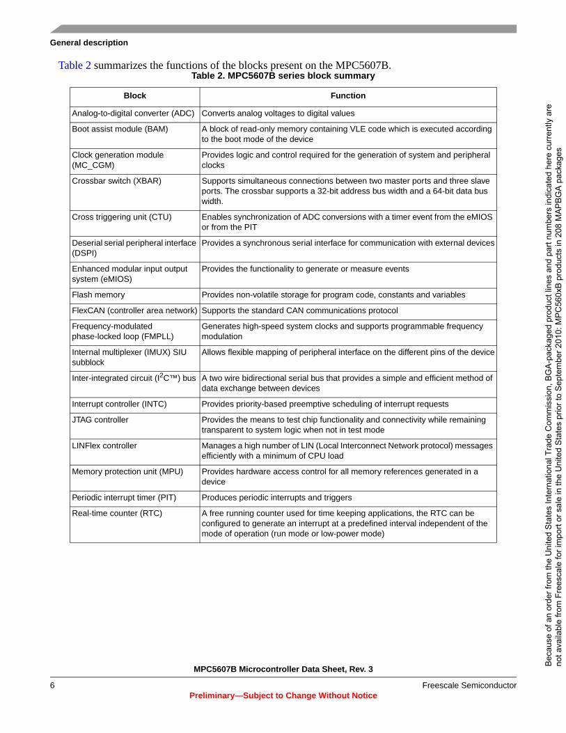
Table 2 summarizes the functions of the blocks present on the MPC5607B.Table 2. MPC5607B series block summary
Block Function
Analog-to-digital converter (ADC) Converts analog voltages to digital values
Boot assist module (BAM) A block of read-only memory containing VLE code which is executed according to the boot mode of the device
Clock generation module (MC_CGM)
Provides logic and control required for the generation of system and peripheral clocks
Crossbar switch (XBAR) Supports simultaneous connections between two master ports and three slave ports. The crossbar supports a 32-bit address bus width and a 64-bit data bus width.
Cross triggering unit (CTU) Enables synchronization of ADC conversions with a timer event from the eMIOS or from the PIT
Deserial serial peripheral interface (DSPI)
Provides a synchronous serial interface for communication with external devices
Enhanced modular input output system (eMIOS)
Provides the functionality to generate or measure events
Flash memory Provides non-volatile storage for program code, constants and variables
FlexCAN (controller area network) Supports the standard CAN communications protocol
Frequency-modulated phase-locked loop (FMPLL)
Generates high-speed system clocks and supports programmable frequency modulation
Internal multiplexer (IMUX) SIU subblock
Allows flexible mapping of peripheral interface on the different pins of the device
Inter-integrated circuit (I2C™) bus A two wire bidirectional serial bus that provides a simple and efficient method of data exchange between devices
Interrupt controller (INTC) Provides priority-based preemptive scheduling of interrupt requests
JTAG controller Provides the means to test chip functionality and connectivity while remaining transparent to system logic when not in test mode
LINFlex controller Manages a high number of LIN (Local Interconnect Network protocol) messages efficiently with a minimum of CPU load
Memory protection unit (MPU) Provides hardware access control for all memory references generated in a device
Periodic interrupt timer (PIT) Produces periodic interrupts and triggers
Real-time counter (RTC) A free running counter used for time keeping applications, the RTC can be configured to generate an interrupt at a predefined interval independent of the mode of operation (run mode or low-power mode)
Bec
ause
of a
n or
der f
rom
the
Uni
ted
Sta
tes
Inte
rnat
iona
l Tra
de C
omm
issi
on, B
GA
-pac
kage
d pr
oduc
t lin
es a
nd p
art n
umbe
rs in
dica
ted
here
cur
rent
ly a
re
not a
vaila
ble
from
Fre
esca
le fo
r im
port
or s
ale
in th
e U
nite
d S
tate
s pr
ior t
o S
epte
mbe
r 201
0: M
PC
560x
B p
rodu
cts
in 2
08 M
AP
BG
A p
acka
ges

Package pinouts
MPC5607B Microcontroller Data Sheet, Rev. 3
Preliminary—Subject to Change Without NoticeFreescale Semiconductor 7
2 Package pinoutsThe available LQFP pinouts and the 208 MAPBGA ballmap are provided in the following figures. For pin signal descriptions, please refer to the device reference manual.
Reset generation module (MC_RGM)
Centralizes reset sources and manages the device reset sequence of the device
Static random-access memory (SRAM)
Provides storage for program code, constants, and variables
System integration unit lite (SIUL) Provides control over all the electrical pad controls and up 32 ports with 16 bits of bidirectional, general-purpose input and output signals and supports up to 32 external interrupts with trigger event configuration
System timer module (STM) Provides a set of output compare events to support AutoSAR and operating system tasks
Table 2. MPC5607B series block summary (continued)
Block Function
Bec
ause
of a
n or
der f
rom
the
Uni
ted
Sta
tes
Inte
rnat
iona
l Tra
de C
omm
issi
on, B
GA
-pac
kage
d pr
oduc
t lin
es a
nd p
art n
umbe
rs in
dica
ted
here
cur
rent
ly a
re
not a
vaila
ble
from
Fre
esca
le fo
r im
port
or s
ale
in th
e U
nite
d S
tate
s pr
ior t
o S
epte
mbe
r 201
0: M
PC
560x
B p
rodu
cts
in 2
08 M
AP
BG
A p
acka
ges

MPC5607B Microcontroller Data Sheet, Rev. 3
Preliminary—Subject to Change Without Notice
Package pinouts
Freescale Semiconductor8
2.1 176LQFP pin configuration
Figure 2. 176 LQFP pin configuration (top view)
1234567891011121314151617181920212223242526272829303132333435363738394041424344
176
175
174
173
172
171
170
169
168
167
166
165
164
163
162
161
160
159
158
157
156
155
154
153
152
151
150
149
148
147
146
145
144
143
142
141
140
139
138
137
136
135
134
133
45 46 47 48 49 50 51 52 53 54 55 56 57 58 59 60 61 62 63 64 65 66 67 68 69 70 71 72 73 74 75 76 77 78 79 80 81 82 83 84 85 86 87 88
1321311301291281271261251241231221211201191181171161151141131121111101091081071061051041031021011009998979695949392919089
PA[11]/GPIO[11]/E0UC[11]/SCL/EIRQ[16]/LIN2RX/ADC1_S[3]PA[10]/GPIO[10]/E0UC[10]/SDA/LIN2TX/ADC1_S[2]PA[9]/GPIO[9]/E0UC[9]/CS2_1/FABPA[8]/GPIO[8]/E0UC[8]/E0UC[14]/EIRQ[3]/ABS[0]/LIN3RXPA[7]/GPIO[7]/E0UC[7]/LIN3TX/EIRQ[2]/ADC1_S[1]PE[13]/GPIO[77]/SOUT_2/E1UC[20]PF[14]/GPIO[94]/CAN4TX/E1UC[27]/CAN1TXPF[15]/GPIO[95]/E1UC[4]/EIRQ[13]/CAN4RX/CAN1RXVDD_HVVSS_HVPG[0]/GPIO[96]/CAN5TX/E1UC[23]PG[1]/GPIO[97]/E1UC[24]/EIRQ[14]/CAN5RXPH[3]/GPIO[115]/E1UC[5]/CS0_1PH[2]/GPIO[114]/E1UC[4]/SCK_1PH[1]/GPIO[113]/E1UC[3]/SOUT_1PH[0]/GPIO[112]/E1UC[2]/SIN_1PG[12]/GPIO[108]/E0UC[26]/SOUT_4PG[13]/GPIO[109]/E0UC[27]/SCK_4PA[3]/GPIO[3]/E0UC[3]/LIN5TX/CS4_1/EIRQ[0]/ADC1_S[0]PI[13]/GPIO[141]/CS1_3/ADC0_S[21]PI[12]/GPIO[140]/CS0_3/ADC0_S20]PI[11]/GPIO[139]/ANS[19]/SIN_3PI[10]/GPIO[138]/ADC0_S[18]PI[9]/GPIO[137]/ADC0_S[17]PI[8]/GPIO[136]/ADC0_S[16]PB[15]/GPIO[31]/E0UC[7]/CS4_0/ADC0_X[3]PD[15]/GPIO[63]/CS2_1/E0UC[27]/ADC0_S[7]PB[14]/GPIO[30]/E0UC[6]/CS3_ 0/ADC0_X[2]PD[14]/GPIO[62]/CS1_1/E0UC[26]/ADC0_S[6]PB[13]/GPIO[29]/E0UC[5]/CS2_0/ADC0_X[1]PD[13]/GPIO[61]/CS0_1/E0UC[25]/ADC0_S[5]PB[12]/GPIO[28]/E0UC[4]/CS1_0/ADC0_X[0]PD[12]/GPIO[60]/CS5_0/E0UC[24]/ADC0_S[4]VDD_HV_ADC1VSS_HV_ADC1PB[11]/GPIO[27]/E0UC[3]/CS0_0/ADC0_S[3]PD[11]/GPIO[59]/ADC0_P[15]/ADC1_P[15]PD[10]/GPIO[58]/ADC0_P[14]/ADC1_P[14]PD[9]/GPIO[57]/ADC0_P[13]/ADC1_P[13]PB[7]/GPIO[23]/ADC0_P[3]/ADC1_P[3]PB[6]/GPIO[22]/ADC0_P[2]/ADC1_P[2]PB[5]/GPIO[21]/ADC0_P[1]/ADC1_P[1]VDD_HV_ADC0VSS_HV_ADC0
LIN0RX/WKUP[11]/SCL/E0UC[31]/GPIO[19]/PB[3]LIN2RX/WKUP[13]/E0UC[7]/GPIO[41]/PC[9]
EIRQ[8]/SCK2/E0UC[14]/GPIO[46]/PC[14]EIRQ[20]/CS0_2/E0UC[15]/GPIO[47]/PC[15]
E1UC[18]/SCK_5/GPIO[148]/PJ[4]VDD_HVVSS_HV
E1UC[17]/SOUT_5/GPIO[127]/PH[15]E1UC[26]/CS0_3/SOUT_4/GPIO[125]/PH[13]
E1UC[27]/CS1_3/SCK_4/GPIO[126]/PH[14]CS0_4/E1UC[30]/GPIO[134]/PI[6]CS1_4/E1UC[31]/GPIO[135]/PI[7]
SIN_3/WKUP[18]/E1UC[14]/GPIO[101]/PG[5]SCK_3/E1UC[13]/GPIO[100]/PG[4]
WKUP[17]/CS0_3/E1UC[12]/GPIO[99]/PG[3]SOUT_3/E1UC[11]/GPIO[98]/PG[2]
MA[2]/WKUP[3]/E0UC[2]/GPIO[2]/PA[2]CAN5RX/WKUP[6]/E0UC[16]/GPIO[64]/PE[0]
WKUP[2]/NMI/E0UC[1]/GPIO[1]/PA[1]CAN5TX/E0UC[17]/GPIO[65]/PE[1]
CAN3TX/E0UC[22]/CAN2TX/GPIO[72]/PE[8]CAN3RX/CAN2RX/WKUP[7]/E0UC[23]/GPIO[73]/PE[9]
EIRQ[10]/E1UC[30]/CS3_1/LIN3TX/GPIO[74]/PE[10]WKUP[19]/E0UC[13]/CLKOUT/E0UC[0]/GPIO[0]/PA[0]LIN3RX/WKUP[14]/CS4_1/E0UC[24]/GPIO[75]/PE[11]
VSS_HVVDD_HVVSS_HV
RESETVSS_LVVDD_LVVDD_BV
LIN7RX/WKUP[21]/SCK_2/E1UC[18]/GPIO[105]/PG[9]EIRQ[15]/CS0_2/LIN7TX/E1UC[17]/GPIO[104]/PG[8]CAN4RX/CAN1RX/WKUP[5]/MA[2]/GPIO[43]/PC[11]
MA[1]/CAN4TX/CAN1TX/GPIO[42]/PC[10]LIN6RX/WKUP[20]/E1UC[30]/E1UC[16]/GPIO[103]/PG[7]
LIN6TX/E1UC[15]/GPIO[102]/PG[6]LIN0TX/E0UC[30]/CAN0TX/GPIO[16]/PB[0]
CAN0RX/WKUP[4]/LIN0RX/E0UC[31]/GPIO[17]/PB[1]CAN2RX/CAN3RX/WKUP[22]/CS5_0/E1UC[1]/GPIO[89]/PF[9]
CAN2TX/CS4_0/CAN3TX/GPIO[88]/PF[8]LIN5TX/E1UC[25]/GPIO[92]/PF[12]E1UC[28]/LIN1TX/GPIO[38]/PC[6]
LIN
1RX
/WK
UP
[12]
/E1U
C[2
9]/G
PIO
[39]
/PC
[7]
E1U
C[2
]/LIN
4TX
/CS
1_0/
GP
IO[9
0]/P
F[1
0]LI
N4R
X/W
KU
P[1
5]/E
1UC
[3]/C
S2_
0/G
PIO
[91]
/PF
[11]
WK
UP
[10]
/E0U
C[1
]/SC
K_0
/CS
0_0/
GP
IO[1
5]/P
A[1
5]LI
N5R
X/W
KU
P[1
6]/E
1UC
[26]
/GP
IO[9
3]/P
F[1
3]E
IRQ
[4]/E
0UC
[0]/C
S0_
0/S
CK
_0/G
PIO
[14]
/PA
[14]
LIN
5RX
/WK
UP
[9]/C
S0_
1/E
0UC
[4]/G
PIO
[4]/P
A[4
]E
0UC
[29]
/SO
UT
_0/G
PIO
[13]
/PA
[13]
EIR
Q[1
7]/S
IN_0
/CS
3_1/
E0U
C[2
8]/G
PIO
[12]
/PA
[12]
VD
D_L
VV
SS
_LV
XTA
LV
SS
_HV
EX
TAL
VD
D_H
VA
DC
1_S
[5]/O
SC
32K
_EX
TAL/
WK
UP
[26]
/AD
C0_
S[1
]/GP
IO[2
5]/P
B[9
]A
DC
1_S
[4]/O
SC
32K
_XTA
L/W
KU
P[2
5]/A
DC
_S[0
]/GP
IO[2
4]/P
B[8
]
AD
C0_
S[6
]/WK
UP
[8]/A
NS
[2]/G
PIO
[26]
/PB
[10]
AD
C0_
S[8
]/CS
3_1/
E0U
C[1
0]/G
PIO
[80]
/PF
[0]
AD
C0_
S[9
]/CS
4_1/
E0U
C[1
1]/G
PIO
[81]
/PF
[1]
AD
C0_
S[1
0]/C
S0_
2/E
0UC
[12]
/GP
IO[8
2]/P
F[2
]A
DC
0_S
[11]
/CS
1_2/
E0U
C[1
3]/G
PIO
[83]
/PF
[3]
AD
C0_
S[1
2]/C
S2_
2/E
0UC
[14]
/GP
IO[8
4]/P
F[4
]A
DC
0_S
[13]
/CS
3_2/
E0U
C[2
2]/G
PIO
[85]
/PF
[5]
AD
C0_
S14
]/CS
1_1/
E0U
C[2
3]/G
PIO
[86]
/PF
[6]
AD
C0_
S[1
5]/C
S2_
1/G
PIO
[87]
/PF
[7]
AD
C0_
S[2
7]/C
S1_
5/G
PIO
[147
]/PJ[
3]A
DC
0_S
[26]
/CS
0_5/
GP
IO[1
46]/P
J[2]
SIN
_5/A
NS
[25]
/GP
IO[1
45]/P
J[1]
AD
C0_
S[2
4]/C
S1_
4/G
PIO
[144
]/PJ[
0]A
DC
0_S
[23]
/CS
0_4/
GP
IO[1
43]/P
I[15]
SIN
_4/A
NS
[22]
/GP
IO[1
42]/P
I[14]
AN
P[4
]/WK
UP
[27]
/GP
IO[4
8]/P
D[0
]A
DC
1_P
[5]/A
DC
0_P
[5]/W
KU
P[2
8]/G
PIO
[49]
/PD
[1]
AD
C1_
P[6
]/AD
C0_
P[6
]/GP
IO[5
0]/P
D[2
]A
DC
1_P
[8]/A
DC
0_P
[7]/G
PIO
[51]
/PD
[3]
AD
C1_
P[8
]/AD
C0_
P[8
]/GP
IO[5
2]/P
D[4
]A
DC
1_P
[9]/A
DC
0_P
[9]/G
PIO
[53]
/PD
[5]
AD
C0_
P[1
0]/A
DC
0_P
[10]
/GP
IO[5
4]/P
D[6
]A
DC
1_P
[11]
/AD
C0_
P[1
1]/G
PIO
[55]
/PD
[7]
VD
D_H
VV
SS
_HV
AD
C1_
P[1
2]/A
DC
0_P
[12]
/GP
IO[5
6]/P
D[8
]A
DC
1_P
[0]/A
DC
0_P
[0]/G
PIO
[20]
/PB
[4]
PB
[2]/G
PIO
[18]
/LIN
0TX
/SD
A/E
0UC
[30]
PC
[8]/G
PIO
[40]
/LIN
2TX
/E0U
C[3
]P
C[1
3]/G
PIO
[45]
/E0U
C[1
3]/S
OU
T_2
PC
[12]
/GP
IO[4
4]/E
0UC
[12]
/EIR
Q[1
9]/S
IN_2
PI[0
]/GP
IO[1
28]/E
0UC
[28]
/LIN
8TX
PI[1
]/GP
IO[1
29]/E
0UC
[29]
/WK
UP
[24]
/LIN
8RX
PI[2
]/GP
IO[1
30]/E
0UC
[30]
/LIN
9TX
PI[3
]/GP
IO[1
31]/E
0UC
[31]
/WK
UP
[23]
/LIN
9RX
PE
[7]/G
PIO
[71]
/E0U
C[2
3]/C
S2_
0/M
A[0
]/EIR
Q[2
3]P
E[6
]/GP
IO[7
0]/E
0UC
[22]
/CS
3_0/
MA
[1]/E
IRQ
[22]
PH
[8]/G
PIO
[120
]/E1U
C[1
0]/C
S2_
2/M
A[0
]P
H[7
]/GP
IO[1
19]/E
1UC
[9]/C
S3_
2/M
A[1
]P
H[6
]/GP
IO[1
18]/E
1UC
[8]/M
A[2
]P
H[5
]/GP
IO[1
17]/E
1UC
[7]
PH
[4]/G
PIO
[116
]/E1U
C[6
]P
E[5
]/GP
IO[6
9]/E
0UC
[21]
/CS
0_1/
MA
[2]
PE
[4]/G
PIO
[68]
/E0U
C[2
0]/S
CK
_1/E
IRQ
[9]
PC
[4]/G
PIO
[36]
/E1U
C[3
1]/E
IRQ
[18]
/SIN
_1/C
AN
3RX
PC
[5]/G
PIO
[37]
/SO
UT
_1/C
AN
3TX
/EIR
Q[7
]P
E[3
]/GP
IO[6
7]/E
0UC
[19]
/SO
UT
_1P
E[2
]/GP
IO[6
6]/E
0UC
[18]
/EIR
Q[2
1]/S
IN_1
PH
[9]/G
PIO
[121
]/TC
KP
C[0
]/GP
IO[3
2]/T
DI
VS
S_L
VV
DD
_LV
VD
D_H
VV
SS
_HV
PC
[1]/G
PIO
[33]
/TD
OP
H[1
0]/G
PIO
[122
]/TM
SPA
[6]/G
PIO
[6]/E
0UC
[6]/C
S1_
1/E
IRQ
[1]/L
IN4R
XPA
[5]/G
PIO
[5]/E
0UC
[5]/L
IN4T
XP
C[2
]/GP
IO[3
4]/S
CK
_1/C
AN
4TX
/EIR
Q[5
]P
C[3
]/GP
IO[3
5]/C
S0_
1/M
A[0
]/EIR
Q[6
]/CA
N4R
X/C
AN
1RX
PI[4
]/GP
IO[1
32]/E
1UC
[28]
/SO
UT
_4P
I[5]/G
PIO
[133
]/E1U
C[2
9]/S
CK
_4P
H[1
2]/G
PIO
[124
]/SC
K_3
/CS
1_4/
E1U
C[2
5]P
H[1
1]/G
PIO
[123
]/SO
UT
_3/C
S0_
4/E
1UC
[5]
PG
[11]
/GP
IO[1
07]/E
0UC
[25]
/CS
0_4
PG
[10]
/GP
IO[1
06]/E
0UC
[24]
/E1U
C[3
1]/S
IN_4
PE
[15]
/GP
IO[7
9]/C
S0_
2/E
1UC
[22]
PE
[14]
/GP
IO[7
8]/S
CK
_2/E
1UC
[21]
/EIR
Q[1
2]P
G[1
5]/G
PIO
[111
]/E1U
C[1
]/LIN
8RX
PG
[14]
/GP
IO[1
10]/E
1UC
[0]/L
IN8T
XP
E[1
2]/G
PIO
[76]
/E1U
C[1
9]/E
IRQ
[11]
/SIN
_2/A
DC
1_S
[7]
176 LQFPTop view
Note:Availability of port pin alternate functions depends on product selection.B
ecau
se o
f an
orde
r fro
m th
e U
nite
d S
tate
s In
tern
atio
nal T
rade
Com
mis
sion
, BG
A-p
acka
ged
prod
uct l
ines
and
par
t num
bers
indi
cate
d he
re c
urre
ntly
are
no
t ava
ilabl
e fro
m F
rees
cale
for i
mpo
rt or
sal
e in
the
Uni
ted
Sta
tes
prio
r to
Sep
tem
ber 2
010:
MP
C56
0xB
pro
duct
s in
208
MA
PB
GA
pac
kage
s

Package pinouts
MPC5607B Microcontroller Data Sheet, Rev. 3
Preliminary—Subject to Change Without NoticeFreescale Semiconductor 9
2.2 144LQFP pin configuration
Figure 3. 144 LQFP pin configuration (top view)
123456789101112131415161718192021222324252627282930313233343536
108107106105104103102101100
999897969594939291908988878685848382818079787776757473
37 38 39 40 41 42 43 44 45 46 47 48 49 50 51 52 53 54 55 56 57 58 59 60 61 62 63 64 65 66 67 68 69 70 71 72
144
143
142
141
140
139
138
137
136
135
134
133
132
131
130
129
128
127
126
125
124
123
122
121
120
119
118
117
116
115
114
113
112
111
110
109
LIN0RX/WKUP[11]/SCL/E0UC[31]/GPIO[19]/PB[3]LIN2RX/WKUP[13]/E0UC[7]/GPIO[41]/PC[9]
EIRQ[8]/SCK2/E0UC[14]/GPIO[46]/PC[14]EIRQ[20]/CS0_2/E0UC[15]/GPIO[47]/PC[15]
SIN_3/WKUP[18]/E1UC[14]/GPIO[101]/PG[5]SCK_3/E1UC[13]/GPIO[100]/PG[4]
WKUP[17]/CS0_3/E1UC[12]/GPIO[99]/PG[3]SOUT_3/E1UC[11]/GPIO[98]/PG[2]
MA[2]/WKUP[3]/E0UC[2]/GPIO[2]/PA[2]CAN5RX/WKUP[6]/E0UC[16]/GPIO[64]/PE[0]
WKUP[2]/NMI[0]/E0UC[1]/GPIO[1]/PA[1]CAN5TX/E0UC[17]/GPIO[65]/PE[1]
CAN3TX/E0UC[22]/CAN2TX/GPIO[72]/PE[8]CAN3RX/CAN2RX/WKUP[7]/E0UC[23]/GPIO[73]/PE[9]
EIRQ[10]/E1UC[30]/CS3_1/LIN3TX/GPIO[74]/PE[10]WKUP[19]/E0UC[13]/CLKOUT/E0UC[0]/GPIO[0]/PA[0]LIN3RX/WKUP[14]/CS4_1/E0UC[24]/GPIO[75]/PE[11]
VSS_HVVDD_HVVSS_HV
RESETVSS_LVVDD_LVVDD_BV
LIN7RX/EIRQ[21]/SCK_2/E1UC[18]/GPIO[105]/PG[9]EIRQ[15]/CS0_2/LIN7TX/E1UC[17]/GPIO[104]/PG[8]CAN4RX/CAN1RX/WKUP[5]/MA[2]/GPIO[43]/PC[11]
MA[1]/CAN4TX/CAN1TX/GPIO[42]/PC[10]LIN6RX/WKUP[20]/E1UC[30]/E1UC[16]/GPIO[103]/PG[7]
LIN6TX/E1UC[15]/GPIO[102]/PG[6]E0UC[30]/CAN0TX/GPIO[16]/PB[0]
LIN0RX/CAN0RX/WKUP[4]/E0UC[31]/GPIO[17]/PB[1]CAN2RX/CAN3RX/WKUP[22]/CS5_0/E1UC[1]/GPIO[89]/PF[9]
CAN2TX/CS4_0/CAN3TX/GPIO[88]/PF[8]LIN5TX/E1UC[25]/GPIO[92]/PF[12]E1UC[28]/LIN1TX/GPIO[38]/PC[6]
PA[11]/GPIO[11]/E0UC[11]/SCL/EIRQ[16]/LIN2RX/ADC1_S[3]PA[10]/GPIO[10]/E0UC[10]/SDA/LIN2TX/ADC1_S[2]PA[9]/GPIO[9]/E0UC[9]/FAB/CS2_1PA[8]/GPIO[8]/E0UC[8]/E0UC[14]/EIRQ[3]/ABS[0]/LIN3RXPA[7]/GPIO[7]/E0UC[7]/LIN3TX/EIRQ[2]/ADC1_S[1]PE[13]/GPIO[77]/SOUT_2/E1UC[20]PF[14]/GPIO[94]/CAN4TX/E1UC[27]/CAN1TXPF[15]/GPIO[95]/E1UC[4]/EIRQ[13]/CAN4RX/CAN1RXVDD_HVVSS_HVPG[0]/GPIO[96]/CAN5TX/E1UC[23]PG[1]/GPIO[97]/E1UC[24]/EIRQ[14]/CAN5RXPH[3]/GPIO[115]/E1UC[5]/CS0_1PH[2]/GPIO[114]/E1UC[4]/SCK_1PH[1]/GPIO[113]/E1UC[3]/SOUT_1PH[0]/GPIO[112]/E1UC[2]/SIN_1PG[12]/GPIO[108]/E0UC[26]/SOUT_4PG[13]/GPIO[109]/E0UC[27]/SCK_4PA[3]/GPIO[3]/E0UC[3]/LIN5TX/EIRQ[0]/CS4_1/ADC1_S[0]PB[15]/GPIO[31]/E0UC[7]/CS4_0/ADC0_X[3]PD[15]/GPIO[63]/CS2_1/E0UC[27]/ADC0_S[7]PB[14]/GPIO[30]/E0UC[6]/CS3_ 0/ADC0_X[2]PD[14]/GPIO[62]/CS1_1/E0UC[26]/ADC0_S[6]PB[13]/GPIO[29]/E0UC[5]/CS2_0/ADC0_X[1]PD[13]/GPIO[61]/CS0_1/E0UC[25]/ADC0_S[5]/GPIO[28]/E0UC[4]/CS1_0VDD_HV_ADC1VSS_HV_ADC1PD[11]/GPIO[59]/ADC0_P[15]/ADC1_P[15]PD[10]/GPIO[58]/ADC0_P[14]/ADC1_P[14]PD[9]/GPIO[57]/ADC0_P[13]/ADC1_P[13]PB[7]/GPIO[23]/ADC0_P[3]/ADC1_P[3]PB[6]/GPIO[22]/ADC0_P[2]/ADC1_P[2]PB[5]/GPIO[21]/ADC0_P[1]/ADC1_P[1]VDD_HV_ADC0VSS_HV_ADC0
LIN
1RX
/WK
UP
[12]
/E1U
C[2
9]/G
PIO
[39]
/PC
[7]
E1U
C[2
]/LIN
4TX
/CS
1_0/
GP
IO[9
0]/P
F[1
0]E
MIO
S[1
]\LIN
4RX
/WK
UP
[15]
/E1U
C[3
]/CS
2_0/
GP
IO[9
1]/P
F[1
1]W
KU
P[1
0]/E
0UC
[1]/S
CK
_0/C
S0_
0/G
PIO
[15]
/PA
[15]
LIN
5RX
/WK
UP
[16]
/E1U
C[2
6]/G
PIO
[93]
/PF
[13]
EIR
Q[4
]/E0U
C[0
]/CS
0_0/
SC
K_0
/GP
IO[1
4]/P
A[1
4]C
SO
_1\L
IN5R
X/W
KU
P[9
]/E0U
C[4
]/GP
IO[4
]/PA
[4]
E0U
C[2
9]/S
OU
T_0
/GP
IO[1
3]/P
A[1
3]C
S3_
1\E
IRQ
[17]
/SIN
_0/E
0UC
[28]
/GP
IO[1
2]/P
A[1
2]V
DD
_LV
VS
S_L
VX
TAL
VS
S_H
VE
XTA
LV
DD
_HV
EIR
Q[2
6]\A
DC
1_S
[5]\O
SC
32K
_EX
TAL/
/WK
UP
[26]
/AD
C0_
S[1
]/GP
IO[2
5]/P
B[9
]
EIR
Q[2
5]\O
SC
32K
_XTA
L//W
KU
P[2
5]/A
NS
[0]/G
PIO
[24]
/PB
[8]
AD
C1_
S[6
]\WK
UP
[8]/A
DC
0_S
[2]/G
PIO
[26]
/PB
[10]
AD
C0_
S[8
]/CS
3_1/
E0U
C[1
0]/G
PIO
[80]
/PF
[0]
AD
C0_
S[9
]/CS
4_1/
E0U
C[1
1]/G
PIO
[81]
/PF
[1]
AD
C0_
S[1
0]/C
S0_
2/E
0UC
[12]
/GP
IO[8
2]/P
F[2
]A
DC
0_S
[11]
/CS
1_2/
E0U
C[1
3]/G
PIO
[83]
/PF
[3]
AD
C0_
S[1
2]/C
S2_
2/E
0UC
[14]
/GP
IO[8
4]/P
F[4
]A
DC
0_S
[13]
/CS
3_2/
E0U
C[2
2]/G
PIO
[85]
/PF
[5]
AD
C0_
S[1
4]/C
S1_
1/E
0UC
[23]
/GP
IO[8
6]/P
F[6
]A
DC
0_S
[15]
/CS
2_1/
GP
IO[8
7]/P
F[7
]E
IRQ
[27]
\AN
P[4
]//W
KU
P[2
7]/G
PIO
[48]
/PD
[0]
EIR
Q[2
8]\A
NP
[5]/W
KU
P[2
8]/G
PIO
[49]
/PD
[1]
AD
C1_
P[7
]/AD
C0_
P[6
]/GP
IO[5
0]/P
D[2
]A
DC
1_P
[7]/A
DC
0_P
[7]/G
PIO
[51]
/PD
[3]
AD
C1_
P[8
]/AD
C0_
P[8
]/GP
IO[5
2]/P
D[4
]A
DC
1_P
[9]/A
DC
0_P
[9]/G
PIO
[53]
/PD
[5]
AD
C1_
P[1
0]/A
DC
0_P
[10]
/GP
IO[5
4]/P
D[6
]A
DC
1_P
[11]
/AD
C0_
P11
]/GP
IO[5
5]/P
D[7
]A
DC
1_P
[12]
/AD
C0_
P[1
2]/G
PIO
[56]
/PD
[8]
AD
C1_
P[0
]/AD
C0_
P[0
]/GP
IO[2
0]/P
B[4
]
PB
[2]/G
PIO
[18]
/LIN
0TX
/SD
A/E
0UC
[30]
PC
[8]/G
PIO
[40]
/LIN
2TX
/E0U
C[3
]P
C[1
3]/G
PIO
[45]
/E0U
C[1
3]/S
OU
T_2
PC
[12]
/GP
IO[4
4]/E
0UC
[12]
/EIR
Q[1
9]/S
IN_2
PE
[7]/G
PIO
[71]
/E0U
C[2
3]/C
S2_
0/M
A[0
]/EIR
Q[2
3]P
E[6
]/GP
IO[7
0]/E
0UC
[22]
/CS
3_0/
MA
[1]/E
IRQ
[22]
PH
[8]/G
PIO
[120
]/E1U
C[1
0]/C
S2_
2/M
A[0
]P
H[7
]/GP
IO[1
19]/E
1UC
[9]/C
S3_
2/M
A[1
]P
H[6
]/GP
IO[1
18]/E
1UC
[8]/M
A[2
]P
H[5
]/GP
IO[1
17]/E
1UC
[7]
PH
[4]/G
PIO
[116
]/E1U
C[6
]P
E[5
]/GP
IO[6
9]/E
0UC
[21]
/CS
0_1/
MA
[2]
PE
[4]/G
PIO
[68]
/E0U
C[2
0]/S
CK
_1/E
IRQ
[9]
PC
[4]/G
PIO
[36]
/E1U
C[3
1]/E
IRQ
[18]
/SIN
_1/C
AN
3RX
PC
[5]/G
PIO
[37]
/SO
UT
_1/C
AN
3TX
/EIR
Q[7
]P
E[3
]/GP
IO[6
7]/E
0UC
[19]
/SO
UT
_1P
E[2
]/GP
IO[6
6]/E
0UC
[18]
/EIR
Q[2
1]/S
IN_1
PH
[9]/G
PIO
[121
]/TC
KP
C[0
]/GP
IO[3
2]/T
DI
VS
S_L
VV
DD
_LV
VD
D_H
VV
SS
_HV
PC
[1]/G
PIO
[33]
/TD
OP
H[1
0]/G
PIO
[122
]/TM
SPA
[6]/G
PIO
[6]/E
0UC
[6]/E
IRQ
[1]/L
IN4R
X/C
S1_
1PA
[5]/G
PIO
[5]/E
0UC
[5]/L
IN4T
XP
C[2
]/GP
IO[3
4]/S
CK
_1/C
AN
4TX
/EIR
Q[5
]P
C[3
]/GP
IO[3
5]/C
S0_
1/M
A[0
]/EIR
Q[6
]/CA
N4R
X/C
AN
1RX
PG
[11]
/GP
IO[1
07]/E
0UC
[25]
/CS
0_4
PG
[10]
/GP
IO[1
06]/E
0UC
[24]
/E1U
C[3
1]/S
IN_4
PE
[15]
/GP
IO[7
9]/C
S0_
2/E
1UC
[22]
PE
[14]
/GP
IO[7
8]/S
CK
_2/E
1UC
[21]
/EIR
Q[1
2]P
G[1
5]/G
PIO
[111
]/E1U
C[1
]/LIN
8RX
PG
[14]
/GP
IO[1
10]/E
1UC
[0]/L
IN8T
XP
E[1
2]/G
PIO
[76]
/E1U
C[1
9]/E
IRQ
[11]
/SIN
_2\A
NS
[7]
144 LQFP
Top view
Note:Availability of port pin alternate functions depends on product selection.
Bec
ause
of a
n or
der f
rom
the
Uni
ted
Sta
tes
Inte
rnat
iona
l Tra
de C
omm
issi
on, B
GA
-pac
kage
d pr
oduc
t lin
es a
nd p
art n
umbe
rs in
dica
ted
here
cur
rent
ly a
re
not a
vaila
ble
from
Fre
esca
le fo
r im
port
or s
ale
in th
e U
nite
d S
tate
s pr
ior t
o S
epte
mbe
r 201
0: M
PC
560x
B p
rodu
cts
in 2
08 M
AP
BG
A p
acka
ges
MPC5607B Microcontroller Data Sheet, Rev. 3
Preliminary—Subject to Change Without Notice
Package pinouts
Freescale Semiconductor10
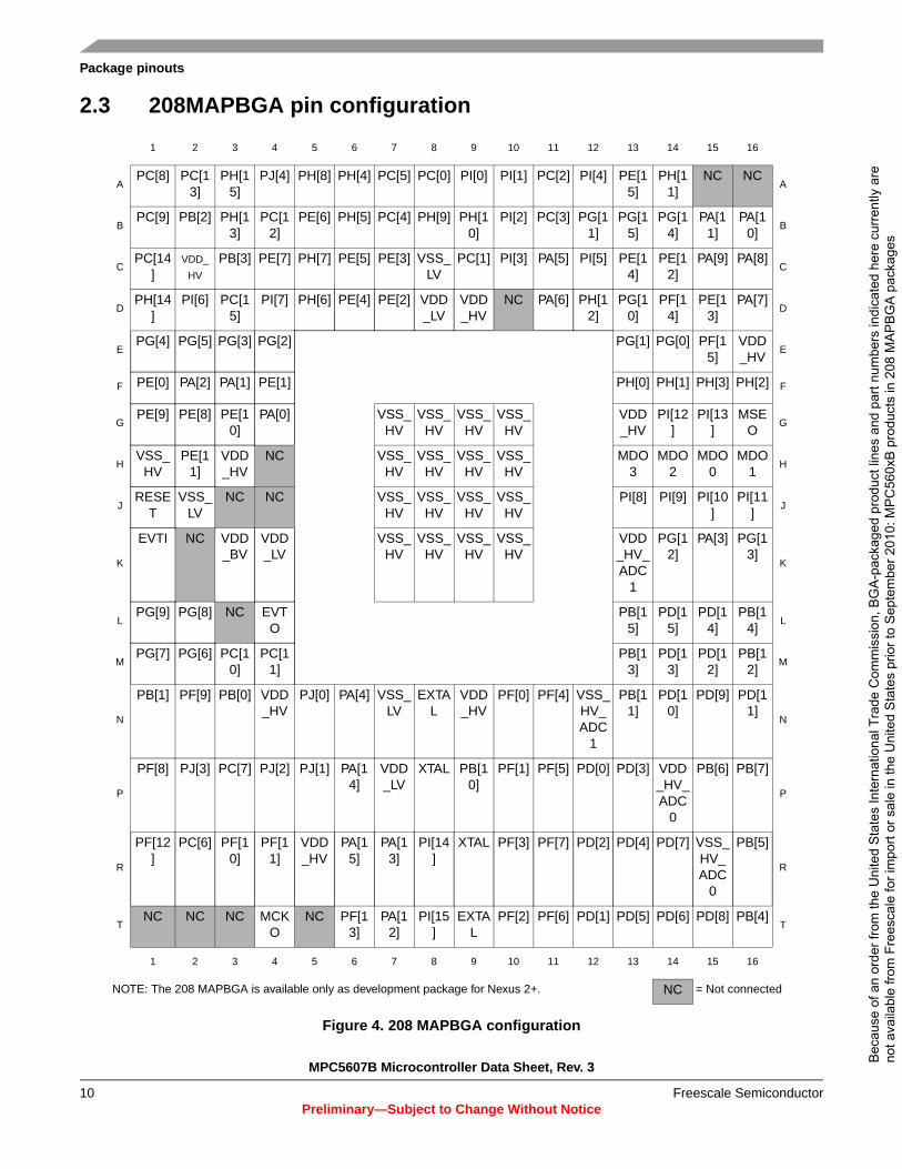
2.3 208MAPBGA pin configuration
Figure 4. 208 MAPBGA configuration
1 2 3 4 5 6 7 8 9 10 11 12 13 14 15 16
APC[8] PC[1
3]PH[1
5]PJ[4] PH[8] PH[4] PC[5] PC[0] PI[0] PI[1] PC[2] PI[4] PE[1
5]PH[1
1]NC NC
A
BPC[9] PB[2] PH[1
3]PC[1
2]PE[6] PH[5] PC[4] PH[9] PH[1
0]PI[2] PC[3] PG[1
1]PG[1
5]PG[1
4]PA[1
1]PA[1
0]B
CPC[14
]VDD_
HV PB[3] PE[7] PH[7] PE[5] PE[3] VSS_
LVPC[1] PI[3] PA[5] PI[5] PE[1
4]PE[1
2]PA[9] PA[8]
C
DPH[14
]PI[6] PC[1
5]PI[7] PH[6] PE[4] PE[2] VDD
_LVVDD_HV
NC PA[6] PH[12]
PG[10]
PF[14]
PE[13]
PA[7]D
EPG[4] PG[5] PG[3] PG[2] PG[1] PG[0] PF[1
5]VDD_HV
E
F PE[0] PA[2] PA[1] PE[1] PH[0] PH[1] PH[3] PH[2] F
GPE[9] PE[8] PE[1
0]PA[0] VSS_
HVVSS_
HVVSS_
HVVSS_
HVVDD_HV
PI[12]
PI[13]
MSEO
G
HVSS_
HVPE[1
1]VDD_HV
NC VSS_HV
VSS_HV
VSS_HV
VSS_HV
MDO3
MDO2
MDO0
MDO1
H
JRESE
TVSS_
LVNC NC VSS_
HVVSS_
HVVSS_
HVVSS_
HVPI[8] PI[9] PI[10
]PI[11
]J
K
EVTI NC VDD_BV
VDD_LV
VSS_HV
VSS_HV
VSS_HV
VSS_HV
VDD_HV_ADC
1
PG[12]
PA[3] PG[13]
K
LPG[9] PG[8] NC EVT
OPB[1
5]PD[1
5]PD[1
4]PB[1
4]L
MPG[7] PG[6] PC[1
0]PC[1
1]PB[1
3]PD[1
3]PD[1
2]PB[1
2]M
N
PB[1] PF[9] PB[0] VDD_HV
PJ[0] PA[4] VSS_LV
EXTAL
VDD_HV
PF[0] PF[4] VSS_HV_ADC
1
PB[11]
PD[10]
PD[9] PD[11]
N
P
PF[8] PJ[3] PC[7] PJ[2] PJ[1] PA[14]
VDD_LV
XTAL PB[10]
PF[1] PF[5] PD[0] PD[3] VDD_HV_ADC
0
PB[6] PB[7]
P
R
PF[12]
PC[6] PF[10]
PF[11]
VDD_HV
PA[15]
PA[13]
PI[14]
XTAL PF[3] PF[7] PD[2] PD[4] PD[7] VSS_HV_ADC
0
PB[5]
R
TNC NC NC MCK
ONC PF[1
3]PA[1
2]PI[15
]EXTA
LPF[2] PF[6] PD[1] PD[5] PD[6] PD[8] PB[4]
T
1 2 3 4 5 6 7 8 9 10 11 12 13 14 15 16
NOTE: The 208 MAPBGA is available only as development package for Nexus 2+. NC = Not connected
Bec
ause
of a
n or
der f
rom
the
Uni
ted
Sta
tes
Inte
rnat
iona
l Tra
de C
omm
issi
on, B
GA
-pac
kage
d pr
oduc
t lin
es a
nd p
art n
umbe
rs in
dica
ted
here
cur
rent
ly a
re
not a
vaila
ble
from
Fre
esca
le fo
r im
port
or s
ale
in th
e U
nite
d S
tate
s pr
ior t
o S
epte
mbe
r 201
0: M
PC
560x
B p
rodu
cts
in 2
08 M
AP
BG
A p
acka
ges

Electrical characteristics
MPC5607B Microcontroller Data Sheet, Rev. 3
Preliminary—Subject to Change Without NoticeFreescale Semiconductor 11
3 Electrical characteristicsThis section contains electrical characteristics of the device as well as temperature and power considerations.
This product contains devices to protect the inputs against damage due to high static voltages. However, it is advisable to take precautions to avoid application of any voltage higher than the specified maximum rated voltages.
To enhance reliability, unused inputs can be driven to an appropriate logic voltage level (VDD or VSS). This could be done by the internal pull-up and pull-down, which is provided by the product for most general purpose pins.
The parameters listed in the following tables represent the characteristics of the device and its demands on the system.
In the tables where the device logic provides signals with their respective timing characteristics, the symbol “CC” for Controller Characteristics is included in the Symbol column.
In the tables where the external system must provide signals with their respective timing characteristics to the device, the symbol “SR” for System Requirement is included in the Symbol column.
CAUTIONAll of the following figures are indicative and must be confirmed during either silicon validation, silicon characterization or silicon reliability trial.
3.1 Parameter classificationThe electrical parameters shown in this supplement are guaranteed by various methods. To give the customer a better understanding, the classifications listed in Table 3 are used and the parameters are tagged accordingly in the tables where appropriate.
NOTEThe classification is shown in the column labeled “C” in the parameter tables where appropriate.
3.2 NVUSRO registerPortions of the device configuration, such as high voltage supply, oscillator margin, and watchdog enable/disable after reset are controlled via bit values in the Non-Volatile User Options Register (NVUSRO) register.
3.2.1 NVUSRO[PAD3V5V] field descriptionTable 4 shows how NVUSRO[PAD3V5V] controls the device configuration.
Table 3. Parameter classifications
Classification tag Tag description
P Those parameters are guaranteed during production testing on each individual device.
C Those parameters are achieved by the design characterization by measuring a statistically relevant sample size across process variations.
T Those parameters are achieved by design characterization on a small sample size from typical devices under typical conditions unless otherwise noted. All values shown in the typical column are within this category.
D Those parameters are derived mainly from simulations.
Bec
ause
of a
n or
der f
rom
the
Uni
ted
Sta
tes
Inte
rnat
iona
l Tra
de C
omm
issi
on, B
GA
-pac
kage
d pr
oduc
t lin
es a
nd p
art n
umbe
rs in
dica
ted
here
cur
rent
ly a
re
not a
vaila
ble
from
Fre
esca
le fo
r im
port
or s
ale
in th
e U
nite
d S
tate
s pr
ior t
o S
epte
mbe
r 201
0: M
PC
560x
B p
rodu
cts
in 2
08 M
AP
BG
A p
acka
ges

MPC5607B Microcontroller Data Sheet, Rev. 3
Preliminary—Subject to Change Without Notice
Electrical characteristics
Freescale Semiconductor12
The DC electrical characteristics are dependent on the PAD3V5V bit value.
3.2.2 NVUSRO[OSCILLATOR_MARGIN] field descriptionTable 5 shows how NVUSRO[OSCILLATOR_MARGIN] controls the device configuration.
The main external crystal oscillator consumption is dependent on the OSCILLATOR_MARGIN bit value.
3.2.3 NVUSRO[WATCHDOG_EN] field descriptionTable 5 shows how NVUSRO[WATCHDOG_EN] controls the device configuration.
Table 4. PAD3V5V field description1
1 See the device reference manual for more information on the NVUSRO register.
Value2
2 '1' is delivery value. It is part of shadow Flash, thus programmable by customer.
Description
0 High voltage supply is 5.0 V
1 High voltage supply is 3.3 V
Table 5. OSCILLATOR_MARGIN field description1
1 See the device reference manual for more information on the NVUSRO register.
Value2
2 '1' is delivery value. It is part of shadow Flash, thus programmable by customer.
Description
0 Low consumption configuration (4 MHz/8 MHz)
1 High margin configuration (4 MHz/16 MHz)
Table 6. WATCHDOG_EN field description1
1 See the device reference manual for more information on the NVUSRO register.
Value2
2 '1' is delivery value. It is part of shadow Flash, thus programmable by customer.
Description
0 Disable after reset
1 Enable after reset
Bec
ause
of a
n or
der f
rom
the
Uni
ted
Sta
tes
Inte
rnat
iona
l Tra
de C
omm
issi
on, B
GA
-pac
kage
d pr
oduc
t lin
es a
nd p
art n
umbe
rs in
dica
ted
here
cur
rent
ly a
re
not a
vaila
ble
from
Fre
esca
le fo
r im
port
or s
ale
in th
e U
nite
d S
tate
s pr
ior t
o S
epte
mbe
r 201
0: M
PC
560x
B p
rodu
cts
in 2
08 M
AP
BG
A p
acka
ges
Electrical characteristics
MPC5607B Microcontroller Data Sheet, Rev. 3
Preliminary—Subject to Change Without NoticeFreescale Semiconductor 13
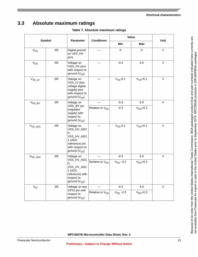
3.3 Absolute maximum ratingsTable 7. Absolute maximum ratings
Symbol Parameter ConditionsValue
UnitMin Max
VSS SR Digital ground on VSS_HV pins
— 0 0 V
VDD SR Voltage on VDD_HV pins with respect to ground (VSS)
— -0.3 6.0 V
VSS_LV SR Voltage on VSS_LV (low voltage digital supply) pins with respect to ground (VSS)
— VSS-0.1 VSS+0.1 V
VDD_BV SR Voltage on VDD_BV pin (regulator supply) with respect to ground (VSS)
— -0.3 6.0 V
Relative to VDD -0.3 VDD+0.3
VSS_ADC SR Voltage on VSS_HV_ADC0, VSS_HV_ADC1 (ADC reference) pin with respect to ground (VSS)
— VSS-0.1 VSS+0.1 V
VDD_ADC SR Voltage on VSS_HV_ADC0, VSS_HV_ADC1 (ADC reference) with respect to ground (VSS)
— -0.3 6.0 V
Relative to VDD VDD −0.3 VDD+0.3
VIN SR Voltage on any GPIO pin with respect to ground (VSS)
— -0.3 6.0 V
Relative to VDD VDD −0.3 VDD+0.3B
ecau
se o
f an
orde
r fro
m th
e U
nite
d S
tate
s In
tern
atio
nal T
rade
Com
mis
sion
, BG
A-p
acka
ged
prod
uct l
ines
and
par
t num
bers
indi
cate
d he
re c
urre
ntly
are
no
t ava
ilabl
e fro
m F
rees
cale
for i
mpo
rt or
sal
e in
the
Uni
ted
Sta
tes
prio
r to
Sep
tem
ber 2
010:
MP
C56
0xB
pro
duct
s in
208
MA
PB
GA
pac
kage
s

MPC5607B Microcontroller Data Sheet, Rev. 3
Preliminary—Subject to Change Without Notice
Electrical characteristics
Freescale Semiconductor14
NOTEStresses exceeding the recommended absolute maximum ratings may cause permanent damage to the device. This is a stress rating only and functional operation of the device at these or any other conditions above those indicated in the operational sections of this specification are not implied. Exposure to absolute maximum rating conditions for extended periods may affect device reliability. During overload conditions (VIN > VDD or VIN < VSS), the voltage on pins with respect to ground (VSS) must not exceed the recommended values.
3.4 Recommended operating conditions
IINJPAD SR Injected input current on any pin during overload condition
— -10 10 mA
IINJSUM SR Absolute sum of all injected input currents during overload condition
— -50 50
IAVGSEG SR Sum of all the static I/O current within a supply segment
VDD = 5.0 V ± 10%, PAD3V5V = 0
70 mA
VDD = 3.3 V ± 10%, PAD3V5V = 1
64
TSTORAGE SR Storage temperature
— -55 150 °C
Table 8. Recommended operating conditions (3.3 V)
Symbol Parameter ConditionsValue
UnitMin Max
VSS SR Digital ground on VSS_HV pins — 0 0 V
VDD1 SR Voltage on VDD_HV pins with respect
to ground (VSS)— 3.0 3.6 V
VSS_LV2 SR Voltage on VSS_LV (low voltage digital
supply) pins with respect to ground (VSS)
— VSS−0.1 VSS+0.1 V
VDD_BV3 SR Voltage on VDD_BV pin (regulator
supply) with respect to ground (VSS)— 3.0 3.6 V
Relative to VDD VDD−0.1 VDD+0.1
Table 7. Absolute maximum ratings (continued)
Symbol Parameter ConditionsValue
UnitMin Max
Bec
ause
of a
n or
der f
rom
the
Uni
ted
Sta
tes
Inte
rnat
iona
l Tra
de C
omm
issi
on, B
GA
-pac
kage
d pr
oduc
t lin
es a
nd p
art n
umbe
rs in
dica
ted
here
cur
rent
ly a
re
not a
vaila
ble
from
Fre
esca
le fo
r im
port
or s
ale
in th
e U
nite
d S
tate
s pr
ior t
o S
epte
mbe
r 201
0: M
PC
560x
B p
rodu
cts
in 2
08 M
AP
BG
A p
acka
ges

Electrical characteristics
MPC5607B Microcontroller Data Sheet, Rev. 3
Preliminary—Subject to Change Without NoticeFreescale Semiconductor 15
VSS_ADC SR Voltage on VSS_HV_ADC0, VSS_HV_ADC1 (ADC reference) pin with respect to ground (VSS)
— VSS−0.1 VSS+0.1 V
VDD_ADC4 SR Voltage on VSS_HV_ADC0,
VSS_HV_ADC1 (ADC reference) with respect to ground (VSS)
— 3.05 3.6 V
Relative to VDD VDD−0.1 VDD+0.1
VIN SR Voltage on any GPIO pin with respect to ground (VSS)
— VSS−0.1 — V
Relative to VDD — VDD+0.1
IINJPAD SR Injected input current on any pin during overload condition
— −5 5 mA
IINJSUM SR Absolute sum of all injected input currents during overload condition
— −50 50
TVDD SR VDD slope to ensure correct power up6 — — 0.25 V/µs
TA SR Ambient temperature under bias fCPU < 64 MHz −40 125 °C
TJ SR Junction temperature under bias — −40 150
1 100 nF capacitance needs to be provided between each VDD/VSS pair2 330 nF capacitance needs to be provided between each VDD_LV/VSS_LV supply pair.3 470 nF capacitance needs to be provided between VDD_BV and the nearest VSS_LV (higher value may be needed
depending on external regulator characteristics).4 100 nF capacitance needs to be provided between VDD_ADC/VSS_ADC pair.5 Full electrical specification cannot be guaranteed when voltage drops below 3.0 V. In particular, ADC electrical
characteristics and I/Os DC electrical specification may not be guaranteed. When voltage drops below VLVDHVL, device is reset.
6 Guaranteed by device validation
Table 9. Recommended operating conditions (5.0 V)
Symbol Parameter ConditionsValue
UnitMin Max
VSS SR Digital ground on VSS_HV pins — 0 0 V
VDD1 SR Voltage on VDD_HV pins with respect to ground (VSS) — 4.5 5.5 V
Voltage drop2 3.0 5.5
VSS_LV3 SR Voltage on VSS_LV (low voltage digital supply) pins with
respect to ground (VSS)— VSS-0.1 VSS+0.1 V
VDD_BV4 SR Voltage on VDD_BV pin (regulator supply) with respect
to ground (VSS)— 4.5 5.5 V
Voltage drop2 3.0 5.5
Relative to VDD VDD-0.1 VDD+0.1
VSS_ADC SR Voltage on VSS_HV_ADC0, VSS_HV_ADC1 (ADC reference) pin with respect to ground (VSS)
— VSS-0.1 VSS+0.1 V
Table 8. Recommended operating conditions (3.3 V) (continued)
Symbol Parameter ConditionsValue
UnitMin Max
Bec
ause
of a
n or
der f
rom
the
Uni
ted
Sta
tes
Inte
rnat
iona
l Tra
de C
omm
issi
on, B
GA
-pac
kage
d pr
oduc
t lin
es a
nd p
art n
umbe
rs in
dica
ted
here
cur
rent
ly a
re
not a
vaila
ble
from
Fre
esca
le fo
r im
port
or s
ale
in th
e U
nite
d S
tate
s pr
ior t
o S
epte
mbe
r 201
0: M
PC
560x
B p
rodu
cts
in 2
08 M
AP
BG
A p
acka
ges

MPC5607B Microcontroller Data Sheet, Rev. 3
Preliminary—Subject to Change Without Notice
Electrical characteristics
Freescale Semiconductor16
NOTERAM data retention is guaranteed wi‘th VDD_LV not below 1.08 V.
VDD_ADC5 SR Voltage on VSS_HV_ADC0, VSS_HV_ADC1 (ADC
reference) with respect to ground (VSS)— 4.5 5.5 V
Voltage drop2 3.0 5.5
Relative to VDD VDD-0.1 VDD+0.1
VIN SR Voltage on any GPIO pin with respect to ground (VSS) — VSS-0.1 - V
Relative to VDD - VDD+0.1
IINJPAD SR Injected input current on any pin during overload condition
— -5 5 mA
IINJSUM SR Absolute sum of all injected input currents during overload condition
— -50 50
TVDD SR VDD slope to ensure correct power up6 — — 0.25 V/µs
— 3 — V/s
TA C-Grade
Part
SR Ambient temperature under bias fCPU < 64 MHz −40 85 °C
TJ C-Grade
Part
SR Junction temperature under bias — −40 110
TA V-Grade
Part
SR Ambient temperature under bias fCPU < 64 MHz −40 105
TJ V-Grade
Part
SR Junction temperature under bias — −40 130
TA M-Grade
Part
SR Ambient temperature under bias fCPU < 60 MHz −40 125
TJ M-Grade
Part
SR Junction temperature under bias — −40 150
1 100 nF capacitance needs to be provided between each VDD/VSS pair2 Full device operation is guaranteed by design when the voltage drops below 4.5V down to 3.6V. However, certain
analog electrical characteristics will not be guaranteed to stay within the stated limits.3 330 nF capacitance needs to be provided between each VDD_LV/VSS_LV supply pair4 470 nF capacitance needs to be provided between VDD_BV and the nearest VSS_LV (higher value may be needed
depending on external regulator characteristics). This decoupling need to be increased as recommended in Section 3.5.1, “External ballast resistor recommendations incase external ballast resistor is planned to be used.
5 100 nF capacitance needs to be provided between VDD_ADC/VSS_ADC pair6 Guaranteed by device validation
Table 9. Recommended operating conditions (5.0 V) (continued)
Symbol Parameter ConditionsValue
UnitMin Max
Bec
ause
of a
n or
der f
rom
the
Uni
ted
Sta
tes
Inte
rnat
iona
l Tra
de C
omm
issi
on, B
GA
-pac
kage
d pr
oduc
t lin
es a
nd p
art n
umbe
rs in
dica
ted
here
cur
rent
ly a
re
not a
vaila
ble
from
Fre
esca
le fo
r im
port
or s
ale
in th
e U
nite
d S
tate
s pr
ior t
o S
epte
mbe
r 201
0: M
PC
560x
B p
rodu
cts
in 2
08 M
AP
BG
A p
acka
ges

Electrical characteristics
MPC5607B Microcontroller Data Sheet, Rev. 3
Preliminary—Subject to Change Without NoticeFreescale Semiconductor 17
3.5 Thermal characteristics
3.5.1 External ballast resistor recommendationsExternal ballast resistor on VDD_BV pin helps in reducing the overall power dissipation inside the device. This resistor is required only when maximum power consumption exceeds the limit imposed by package thermal characteristics.
As stated in Table 10 LQFP thermal characteristics, considering thermal resistance of LQFP144 as 48.3 °C/W, at ambient TA = 125 °C, the junction temp Tj will cross 150 °C if total power dissipation > (150 - 125)/48.3 = 517 mW. Therefore, total device current IDDMAX at 125 °C/5.5V must not exceed 94.1 mA (i.e. PD/VDD). Assuming an average IDD(VDD_HV) of 15-20 mA consumption typically during device RUN mode, the LV domain consumption IDD(VDD_BV) is thus limited to IDDMAX - IDD(VDD_HV) i.e. 80 mA.
Therefore, respecting the maximum power allowed as explained in Section 3.5.2, “Package thermal characteristics, it is recommended to use this resistor only in the 125 °C/5.5V operating corner as per the following guidelines:
• If IDD(VDD_BV) < 80 mA, then no resistor is required.• If 80 mA < IDD(VDD_BV) < 90 mA, then 4 Ohm resistor can be used along with 14.7 µf decoupling.• If IDD(VDD_BV) > 90 mA, then 8 Ohm resistor can be used along with 33 µf decoupling.
Using resistance in the range of 4-8 Ohm, the gain will be around 10-20% of total consumption on VDD_BV. For example, if 8 Ohm resistor is used, then power consumption when IDD(VDD_BV) is 110 mA is equivalent to power consumption when IDD(VDD_BV) is 90 mA (approximately) when resistor not used.
3.5.2 Package thermal characteristics
Table 10. LQFP thermal characteristics1
1 Thermal characteristics are targets based on simulation that are subject to change per device characterization.
Symbol C Parameter Conditions2
2 VDD = 3.3 V ± 10% / 5.0 V ± 10%, TA = −40 to 125 °C.
Pin countValue3
3 All values need to be confirmed during device validation.
UnitMin Typ Max
RθJA CC D Thermal resistance, junction-to-ambient natural convection4
4 Junction-to-ambient thermal resistance determined per JEDEC JESD51-3 and JESD51-6. Thermal test board meets JEDEC specification for this package. When Greek letters are not available, the symbols are typed as RthJA and RthJMA.
Single-layer board—1s
100 — — 64 °C/W
144 — — 64
176 — — 64
Four-layer board—2s2p
100 — — 49.7
144 — — 48.3
176 — — 47.3
Bec
ause
of a
n or
der f
rom
the
Uni
ted
Sta
tes
Inte
rnat
iona
l Tra
de C
omm
issi
on, B
GA
-pac
kage
d pr
oduc
t lin
es a
nd p
art n
umbe
rs in
dica
ted
here
cur
rent
ly a
re
not a
vaila
ble
from
Fre
esca
le fo
r im
port
or s
ale
in th
e U
nite
d S
tate
s pr
ior t
o S
epte
mbe
r 201
0: M
PC
560x
B p
rodu
cts
in 2
08 M
AP
BG
A p
acka
ges

MPC5607B Microcontroller Data Sheet, Rev. 3
Preliminary—Subject to Change Without Notice
Electrical characteristics
Freescale Semiconductor18
3.5.3 Power considerationsThe average chip-junction temperature, TJ, in degrees Celsius, may be calculated using Equation 1:
TJ = TA + (PD x RθJA) Eqn. 1
Where:TA is the ambient temperature in °C.RθJA is the package junction-to-ambient thermal resistance, in °C/W.PD is the sum of PINT and PI/O (PD = PINT + PI/O).PINT is the product of IDD and VDD, expressed in watts. This is the chip internal power.PI/O represents the power dissipation on input and output pins; user determined.
Most of the time for the applications, PI/O< PINT and may be neglected. On the other hand, PI/O may be significant, if the device is configured to continuously drive external modules and/or memories.
An approximate relationship between PD and TJ (if PI/O is neglected) is given by:
PD = K / (TJ + 273 °C) Eqn. 2
Therefore, solving equations 1 and 2:
K = PD x (TA + 273 °C) + RθJA x PD2 Eqn. 3
Where: K is a constant for the particular part, which may be determined from Equation 3 by measuring PD (at equilibrium) for a known TA. Using this value of K, the values of PD and TJ may be obtained by solving equations 1 and 2 iteratively for any value of TA.
3.6 I/O pad electrical characteristics
3.6.1 I/O pad typesThe device provides four main I/O pad types depending on the associated alternate functions:
• Slow pads - are the most common pads, providing a good compromise between transition time and low electromagnetic emission.
• Medium pads - provide transition fast enough for the serial communication channels with controlled current to reduce electromagnetic emission.
Table 11. 208 MAPBGA thermal characteristics1
1 Thermal characteristics are targets based on simulation that are subject to change per device characterization.
Symbol C Parameter Conditions Value Unit
RθJA CC — Thermal resistance, junction-to-ambient natural convection2
2 Junction-to-ambient thermal resistance determined per JEDEC JESD51-3 and JESD51-6. Thermal test board meets JEDEC specification for this package. When Greek letters are not available, the symbols are typed as RthJA and RthJMA.
Single-layer board—1s
TBD °C/W
Four-layer board—2s2p
Bec
ause
of a
n or
der f
rom
the
Uni
ted
Sta
tes
Inte
rnat
iona
l Tra
de C
omm
issi
on, B
GA
-pac
kage
d pr
oduc
t lin
es a
nd p
art n
umbe
rs in
dica
ted
here
cur
rent
ly a
re
not a
vaila
ble
from
Fre
esca
le fo
r im
port
or s
ale
in th
e U
nite
d S
tate
s pr
ior t
o S
epte
mbe
r 201
0: M
PC
560x
B p
rodu
cts
in 2
08 M
AP
BG
A p
acka
ges

Electrical characteristics
MPC5607B Microcontroller Data Sheet, Rev. 3
Preliminary—Subject to Change Without NoticeFreescale Semiconductor 19
• Fast pads - provide maximum speed. These are used for improved Nexus debugging capability.• Input only pads - are associated with ADC channels and 32 kHz low power external crystal oscillator providing low
input leakage.
Medium and Fast pads can use slow configuration to reduce electromagnetic emission, at the cost of reducing AC performance.
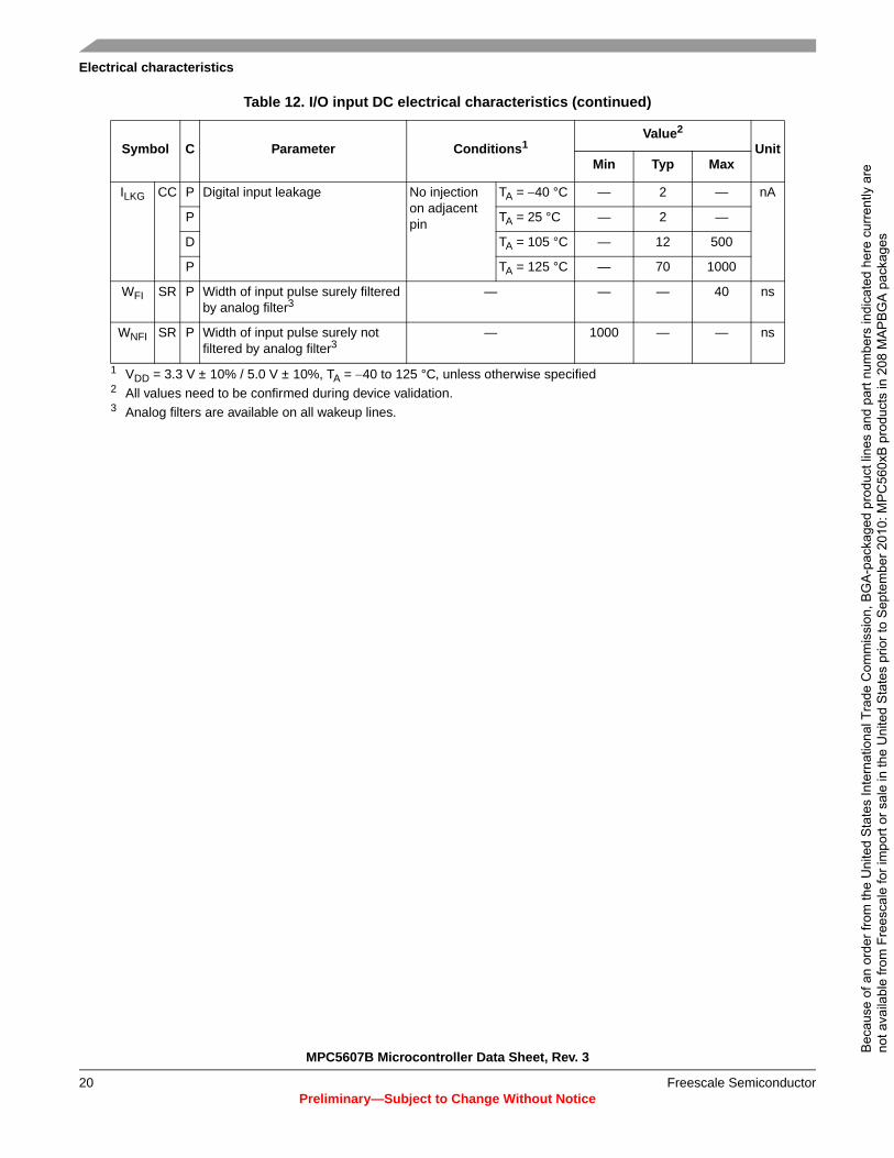
3.6.2 I/O input DC characteristicsTable 12 provides input DC electrical characteristics as described in Figure 5.
Figure 5. I/O input DC electrical characteristics definition
Table 12. I/O input DC electrical characteristics
Symbol C Parameter Conditions1Value2
UnitMin Typ Max
VIH SR P Input high level CMOS (Schmitt Trigger)
— 0.65VDD — VDD+0.4 V
VIL SR P Input low level CMOS (Schmitt Trigger)
— −0.4 — 0.35VDD
VHYS CC C Input hysteresis CMOS (Schmitt Trigger)
— 0.1VDD — —
VIL
VIN
VIH
PDIx = ‘1
VDD
VHYS
(GPDI register of SIUL)
PDIx = ‘0’
Bec
ause
of a
n or
der f
rom
the
Uni
ted
Sta
tes
Inte
rnat
iona
l Tra
de C
omm
issi
on, B
GA
-pac
kage
d pr
oduc
t lin
es a
nd p
art n
umbe
rs in
dica
ted
here
cur
rent
ly a
re
not a
vaila
ble
from
Fre
esca
le fo
r im
port
or s
ale
in th
e U
nite
d S
tate
s pr
ior t
o S
epte
mbe
r 201
0: M
PC
560x
B p
rodu
cts
in 2
08 M
AP
BG
A p
acka
ges
MPC5607B Microcontroller Data Sheet, Rev. 3
Preliminary—Subject to Change Without Notice
Electrical characteristics
Freescale Semiconductor20
ILKG CC P Digital input leakage No injection on adjacent pin
TA = −40 °C — 2 — nA
P TA = 25 °C — 2 —
D TA = 105 °C — 12 500
P TA = 125 °C — 70 1000
WFI SR P Width of input pulse surely filtered by analog filter3
— — — 40 ns
WNFI SR P Width of input pulse surely not filtered by analog filter3
— 1000 — — ns
1 VDD = 3.3 V ± 10% / 5.0 V ± 10%, TA = −40 to 125 °C, unless otherwise specified2 All values need to be confirmed during device validation.3 Analog filters are available on all wakeup lines.
Table 12. I/O input DC electrical characteristics (continued)
Symbol C Parameter Conditions1Value2
UnitMin Typ Max
Bec
ause
of a
n or
der f
rom
the
Uni
ted
Sta
tes
Inte
rnat
iona
l Tra
de C
omm
issi
on, B
GA
-pac
kage
d pr
oduc
t lin
es a
nd p
art n
umbe
rs in
dica
ted
here
cur
rent
ly a
re
not a
vaila
ble
from
Fre
esca
le fo
r im
port
or s
ale
in th
e U
nite
d S
tate
s pr
ior t
o S
epte
mbe
r 201
0: M
PC
560x
B p
rodu
cts
in 2
08 M
AP
BG
A p
acka
ges

Electrical characteristics
MPC5607B Microcontroller Data Sheet, Rev. 3
Preliminary—Subject to Change Without NoticeFreescale Semiconductor 21
3.6.3 I/O output DC characteristicsThe following tables provide DC characteristics for bidirectional pads:
• Table 13 provides weak pull figures. Both pull-up and pull-down resistances are supported.• Table 15 provides output driver characteristics for I/O pads when in SLOW configuration.• Table 16 provides output driver characteristics for I/O pads when in MEDIUM configuration.• Table 14 provides output driver characteristics for I/O pads when in FAST configuration.
Table 13. I/O pull-up/pull-down DC electrical characteristics
Symbol C Parameter Conditions1
1 VDD = 3.3 V ± 10% / 5.0 V ± 10%, TA = −40 to 125 °C, unless otherwise specified.
ValueUnit
Min Typ Max
|IWPU| CC P Weak pull-up current absolute value
VIN = VIL, VDD = 5.0 V ± 10%
PAD3V5V = 0
10 — 150 µA
C PAD3V5V = 12
2 The configuration PAD3V5 = 1 when VDD = 5 V is only a transient configuration during power-up. All pads but RESET and Nexus output (MDOx, EVTO, MCKO) are configured in input or in high impedance state.
10 — 250
P VIN = VIL, VDD = 3.3 V ± 10%
PAD3V5V = 1
10 — 150
|IWPD| CC P Weak pull-down current absolute value
VIN = VIH, VDD = 5.0 V ± 10%
PAD3V5V = 0
10 — 150 µA
C PAD3V5V = 1
10 — 250
P VIN = VIH, VDD = 3.3 V ± 10%
PAD3V5V = 1
10 — 150
Bec
ause
of a
n or
der f
rom
the
Uni
ted
Sta
tes
Inte
rnat
iona
l Tra
de C
omm
issi
on, B
GA
-pac
kage
d pr
oduc
t lin
es a
nd p
art n
umbe
rs in
dica
ted
here
cur
rent
ly a
re
not a
vaila
ble
from
Fre
esca
le fo
r im
port
or s
ale
in th
e U
nite
d S
tate
s pr
ior t
o S
epte
mbe
r 201
0: M
PC
560x
B p
rodu
cts
in 2
08 M
AP
BG
A p
acka
ges
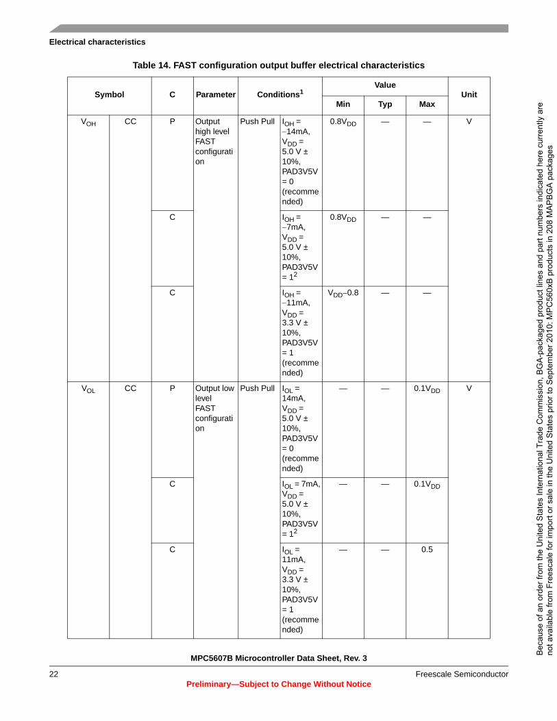
MPC5607B Microcontroller Data Sheet, Rev. 3
Preliminary—Subject to Change Without Notice
Electrical characteristics
Freescale Semiconductor22
Table 14. FAST configuration output buffer electrical characteristics
Symbol C Parameter Conditions1Value
UnitMin Typ Max
VOH CC P Output high levelFAST configuration
Push Pull IOH = −14mA,VDD = 5.0 V ± 10%, PAD3V5V = 0(recommended)
0.8VDD — — V
C IOH = −7mA,VDD = 5.0 V ± 10%, PAD3V5V = 12
0.8VDD — —
C IOH = −11mA,VDD = 3.3 V ± 10%, PAD3V5V = 1 (recommended)
VDD−0.8 — —
VOL CC P Output low levelFAST configuration
Push Pull IOL = 14mA,VDD = 5.0 V ± 10%, PAD3V5V = 0(recommended)
— — 0.1VDD V
C IOL = 7mA,VDD = 5.0 V ± 10%, PAD3V5V = 12
— — 0.1VDD
C IOL = 11mA,VDD = 3.3 V ± 10%, PAD3V5V = 1 (recommended)
— — 0.5B
ecau
se o
f an
orde
r fro
m th
e U
nite
d S
tate
s In
tern
atio
nal T
rade
Com
mis
sion
, BG
A-p
acka
ged
prod
uct l
ines
and
par
t num
bers
indi
cate
d he
re c
urre
ntly
are
no
t ava
ilabl
e fro
m F
rees
cale
for i
mpo
rt or
sal
e in
the
Uni
ted
Sta
tes
prio
r to
Sep
tem
ber 2
010:
MP
C56
0xB
pro
duct
s in
208
MA
PB
GA
pac
kage
s
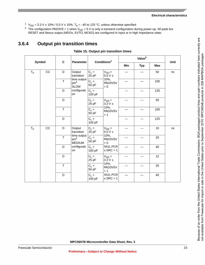
Electrical characteristics
MPC5607B Microcontroller Data Sheet, Rev. 3
Preliminary—Subject to Change Without NoticeFreescale Semiconductor 23
3.6.4 Output pin transition times
1 VDD = 3.3 V ± 10% / 5.0 V ± 10%, TA = −40 to 125 °C, unless otherwise specified2 The configuration PAD3V5 = 1 when VDD = 5 V is only a transient configuration during power-up. All pads but
RESET and Nexus output (MDOx, EVTO, MCKO) are configured in input or in high impedance state.
Table 15. Output pin transition times
Symbol C Parameter Conditions1Value2
UnitMin Typ Max
Ttr CC D Output transition time output pin3
SLOW configuration
CL = 25 pF
VDD = 5.0 V ± 10%,PAD3V5V = 0
— — 50 ns
T CL = 50 pF
— — 100
D CL = 100 pF
— — 125
D CL = 25 pF
VDD = 3.3 V ± 10%, PAD3V5V = 1
— — 50
T CL = 50 pF
— — 100
D CL = 100 pF
— — 125
Ttr CC D Output transition time output pin3
MEDIUM configuration
CL = 25 pF
VDD = 5.0 V ± 10%, PAD3V5V = 0SIUL.PCRx.SRC = 1
— — 10 ns
T CL = 50 pF
— — 20
D CL = 100 pF
— — 40
D CL = 25 pF
VDD = 3.3 V ± 10%, PAD3V5V = 1SIUL.PCRx.SRC = 1
— — 12
T CL = 50 pF
— — 25
D CL = 100 pF
— — 40
Bec
ause
of a
n or
der f
rom
the
Uni
ted
Sta
tes
Inte
rnat
iona
l Tra
de C
omm
issi
on, B
GA
-pac
kage
d pr
oduc
t lin
es a
nd p
art n
umbe
rs in
dica
ted
here
cur
rent
ly a
re
not a
vaila
ble
from
Fre
esca
le fo
r im
port
or s
ale
in th
e U
nite
d S
tate
s pr
ior t
o S
epte
mbe
r 201
0: M
PC
560x
B p
rodu
cts
in 2
08 M
AP
BG
A p
acka
ges

MPC5607B Microcontroller Data Sheet, Rev. 3
Preliminary—Subject to Change Without Notice
Electrical characteristics
Freescale Semiconductor24
3.6.5 I/O pad current specificationThe I/O pads are distributed across the I/O supply segment. Each I/O supply segment is associated to a VDD/VSS supply pair as described in Table 16.
Table 17 provides I/O consumption figures.
In order to ensure device reliability, the average current of the I/O on a single segment should remain below the IAVGSEG maximum value.
In order to ensure device functionality, the sum of the dynamic and static current of the I/O on a single segment should remain below the IDYNSEG maximum value.
Ttr CC D Output transition time output pin3
FAST configuration
CL = 25 pF
VDD = 5.0 V ± 10%, PAD3V5V = 0
— — 4 ns
CL = 50 pF
— — 6
CL = 100 pF
— — 12
CL = 25 pF
VDD = 3.3 V ± 10%, PAD3V5V = 1
— — 4
CL = 50 pF
— — 7
CL = 100 pF
— — 12
1 VDD = 3.3 V ± 10% / 5.0 V ± 10%, TA = −40 to 125 °C, unless otherwise specified2 All values need to be confirmed during device validation.3 CL includes device and package capacitances (CPKG < 5 pF).
Table 16. I/O supply segments
PackageSupply segment
1 2 3 4 5 6 7 8
208 MAPBGA1
1 208 MAPBGA available only as development package for Nexus2+
Equivalent to 176 LQFP segment pad distribution MCKO MDOn/MSEO
176 LQFP pin7– pin27 pin28 – pin57
pin59 – pin85
pin86 – pin123
pin124 – pin150
pin151 – pin6
144 LQFP pin20 – pin49
pin51 – pin99
pin100 – pin122
pin 123 – pin19
— — — —
100 LQFP pin16 – pin35
pin37 – pin69
pin70 – pin83
pin84 – pin15
— — — —
Table 15. Output pin transition times (continued)
Symbol C Parameter Conditions1Value2
UnitMin Typ Max
Bec
ause
of a
n or
der f
rom
the
Uni
ted
Sta
tes
Inte
rnat
iona
l Tra
de C
omm
issi
on, B
GA
-pac
kage
d pr
oduc
t lin
es a
nd p
art n
umbe
rs in
dica
ted
here
cur
rent
ly a
re
not a
vaila
ble
from
Fre
esca
le fo
r im
port
or s
ale
in th
e U
nite
d S
tate
s pr
ior t
o S
epte
mbe
r 201
0: M
PC
560x
B p
rodu
cts
in 2
08 M
AP
BG
A p
acka
ges

Electrical characteristics
MPC5607B Microcontroller Data Sheet, Rev. 3
Preliminary—Subject to Change Without NoticeFreescale Semiconductor 25
Table 17. I/O consumption
Symbol C Parameter Conditions1Value2
UnitMin Typ Max
IDYNSEG SR D Sum of all the dynamic and static I/O current within a supply segment
VDD = 5.0 V ± 10%, PAD3V5V = 0
— — 110 mA
VDD = 3.3 V ± 10%, PAD3V5V = 1
— — 65
ISWTSLW,3 CC D Dynamic
I/O current for SLOW configuration
CL = 25 pF
VDD = 5.0 V ± 10%,PAD3V5V = 0
— — 20 mA
VDD = 3.3 V ± 10%,PAD3V5V = 1
— — 16
ISWTMED3 CC D Dynamic
I/O current for MEDIUM configuration
CL = 25 pF
VDD = 5.0 V ± 10%,PAD3V5V = 0
— — 29 mA
VDD = 3.3 V ± 10%,PAD3V5V = 1
— — 17
ISWTFST3 CC D Dynamic
I/O current for FAST configuration
CL = 25 pF
VDD = 5.0 V ± 10%,PAD3V5V = 0
— — 110 mA
VDD = 3.3 V ± 10%,PAD3V5V = 1
— — 50
Bec
ause
of a
n or
der f
rom
the
Uni
ted
Sta
tes
Inte
rnat
iona
l Tra
de C
omm
issi
on, B
GA
-pac
kage
d pr
oduc
t lin
es a
nd p
art n
umbe
rs in
dica
ted
here
cur
rent
ly a
re
not a
vaila
ble
from
Fre
esca
le fo
r im
port
or s
ale
in th
e U
nite
d S
tate
s pr
ior t
o S
epte
mbe
r 201
0: M
PC
560x
B p
rodu
cts
in 2
08 M
AP
BG
A p
acka
ges

MPC5607B Microcontroller Data Sheet, Rev. 3
Preliminary—Subject to Change Without Notice
Electrical characteristics
Freescale Semiconductor26
IRMSSLW CC D Root medium square I/O current for SLOW configuration
CL = 25 pF, 2 MHz
VDD = 5.0 V ± 10%,PAD3V5V = 0
— — 2.3 mA
CL = 25 pF, 4 MHz
— — 3.2
CL = 100 pF, 2 MHz
— — 6.6
CL = 25 pF, 2 MHz
VDD = 3.3 V ± 10%,PAD3V5V = 1
— — 1.6
CL = 25 pF, 4 MHz
— — 2.3
CL = 100 pF, 2 MHz
— — 4.7
IRMSMED CC D Root medium square I/O current for MEDIUM configuration
CL = 25 pF, 13 MHz
VDD = 5.0 V ± 10%, PAD3V5V = 0
— — 6.6 mA
CL = 25 pF, 40 MHz
— — 13.4
CL = 100 pF, 13 MHz
— — 18.3
CL = 25 pF, 13 MHz
VDD = 3.3 V ± 10%, PAD3V5V = 1
— — 5
CL = 25 pF, 40 MHz
— — 8.5
CL = 100 pF, 13 MHz
— — 11
Table 17. I/O consumption (continued)
Symbol C Parameter Conditions1Value2
UnitMin Typ Max
Bec
ause
of a
n or
der f
rom
the
Uni
ted
Sta
tes
Inte
rnat
iona
l Tra
de C
omm
issi
on, B
GA
-pac
kage
d pr
oduc
t lin
es a
nd p
art n
umbe
rs in
dica
ted
here
cur
rent
ly a
re
not a
vaila
ble
from
Fre
esca
le fo
r im
port
or s
ale
in th
e U
nite
d S
tate
s pr
ior t
o S
epte
mbe
r 201
0: M
PC
560x
B p
rodu
cts
in 2
08 M
AP
BG
A p
acka
ges

Electrical characteristics
MPC5607B Microcontroller Data Sheet, Rev. 3
Preliminary—Subject to Change Without NoticeFreescale Semiconductor 27
3.7 nRSTIN electrical characteristicsThe device implements a dedicated bidirectional RESET pin.
IRMSFST CC D Root medium square I/O current for FAST configuration
CL = 25 pF, 40 MHz
VDD = 5.0 V ± 10%, PAD3V5V = 0
— — 22 mA
CL = 25 pF, 64 MHz
— — 33
CL = 100 pF, 40 MHz
— — 56
CL = 25 pF, 40 MHz
VDD = 3.3 V ± 10%, PAD3V5V = 1
— — 14
CL = 25 pF, 64 MHz
— — 20
CL = 100 pF, 40 MHz
— — 35
IAVGSEG SR D Sum of all the static I/O current within a supply segment
VDD = 5.0 V ± 10%, PAD3V5V = 0
— — 70 mA
VDD = 3.3 V ± 10%, PAD3V5V = 1
— — 65
1 VDD = 3.3 V ± 10% / 5.0 V ± 10%, TA = −40 to125 °C, unless otherwise specified2 All values need to be confirmed during device validation.3 Stated maximum values represent peak consumption that lasts only a few ns during I/O transition.
Table 17. I/O consumption (continued)
Symbol C Parameter Conditions1Value2
UnitMin Typ Max
Bec
ause
of a
n or
der f
rom
the
Uni
ted
Sta
tes
Inte
rnat
iona
l Tra
de C
omm
issi
on, B
GA
-pac
kage
d pr
oduc
t lin
es a
nd p
art n
umbe
rs in
dica
ted
here
cur
rent
ly a
re
not a
vaila
ble
from
Fre
esca
le fo
r im
port
or s
ale
in th
e U
nite
d S
tate
s pr
ior t
o S
epte
mbe
r 201
0: M
PC
560x
B p
rodu
cts
in 2
08 M
AP
BG
A p
acka
ges

MPC5607B Microcontroller Data Sheet, Rev. 3
Preliminary—Subject to Change Without Notice
Electrical characteristics
Freescale Semiconductor28
Figure 6. Start-up reset requirements
Figure 7. Noise filtering on reset signal
VIL
VDD
device reset forced by nRSTIN
VDDMIN
nRSTIN
VIH
device start-up phase
VRSTIN
VIL
VIH
VDD
filtered by hysteresis
filtered by lowpass filter
WFRST
WNFRST
hw_rst
‘1’
‘0’filtered by lowpass filter
WFRST
unknown resetstate device under hardware reset
Bec
ause
of a
n or
der f
rom
the
Uni
ted
Sta
tes
Inte
rnat
iona
l Tra
de C
omm
issi
on, B
GA
-pac
kage
d pr
oduc
t lin
es a
nd p
art n
umbe
rs in
dica
ted
here
cur
rent
ly a
re
not a
vaila
ble
from
Fre
esca
le fo
r im
port
or s
ale
in th
e U
nite
d S
tate
s pr
ior t
o S
epte
mbe
r 201
0: M
PC
560x
B p
rodu
cts
in 2
08 M
AP
BG
A p
acka
ges

Electrical characteristics
MPC5607B Microcontroller Data Sheet, Rev. 3
Preliminary—Subject to Change Without NoticeFreescale Semiconductor 29
Table 18. Reset electrical characteristics
Symbol C Parameter Conditions1
1 VDD = 3.3 V ± 10% / 5.0 V ± 10%, TA = −40 to 125 °C, unless otherwise specified
Value2
2 All values need to be confirmed during device validation.
UnitMin Typ Max
VIH SR P Input High Level CMOS (Schmitt Trigger)
— 0.65VDD — VDD+0.4 V
VIL SR P Input low Level CMOS (Schmitt Trigger)
— −0.4 — 0.35VDD V
VHYS CC C Input hysteresis CMOS (Schmitt Trigger)
— 0.1VDD — — V
VOL CC P Output low level Push Pull, IOL = 2mA,VDD = 5.0 V ± 10%, PAD3V5V = 0(recommended)
— — 0.1VDD V
Push Pull, IOL = 1mA,VDD = 5.0 V ± 10%, PAD3V5V = 13
3 This is a transient configuration during power-up, up to the end of reset PHASE2 (refer to RGM module section of the device reference manual).
— — 0.1VDD
Push Pull, IOL = 1mA,VDD = 3.3 V ± 10%, PAD3V5V = 1 (recommended)
— — 0.5
Ttr CC D Output transition time output pin4
MEDIUM configuration
4 CL includes device and package capacitance (CPKG < 5 pF).
CL = 25pF,VDD = 5.0 V ± 10%, PAD3V5V = 0
— — 10 ns
CL = 50pF,VDD = 5.0 V ± 10%, PAD3V5V = 0
— — 20
CL = 100pF,VDD = 5.0 V ± 10%, PAD3V5V = 0
— — 40
CL = 25pF,VDD = 3.3 V ± 10%, PAD3V5V = 1
— — 12
CL = 50pF,VDD = 3.3 V ± 10%, PAD3V5V = 1
— — 25
CL = 100pF,VDD = 3.3 V ± 10%, PAD3V5V = 1
— — 40
WFRST SR P nRSTIN input filtered pulse
— — — 40 ns
WNFRST SR P nRSTIN input not filtered pulse
— 1000 — — ns
|IWPU| CC P Weak pull-up current absolute value
VDD = 3.3 V ± 10%, PAD3V5V = 1 10 — 150 µA
VDD = 5.0 V ± 10%, PAD3V5V = 0 10 — 150
VDD = 5.0 V ± 10%, PAD3V5V = 15
5 The configuration PAD3V5 = 1 when VDD = 5 V is only transient configuration during power-up. All pads but RESET and Nexus output (MDOx, EVTO, MCKO) are configured in input or in high impedance state.
10 — 250B
ecau
se o
f an
orde
r fro
m th
e U
nite
d S
tate
s In
tern
atio
nal T
rade
Com
mis
sion
, BG
A-p
acka
ged
prod
uct l
ines
and
par
t num
bers
indi
cate
d he
re c
urre
ntly
are
no
t ava
ilabl
e fro
m F
rees
cale
for i
mpo
rt or
sal
e in
the
Uni
ted
Sta
tes
prio
r to
Sep
tem
ber 2
010:
MP
C56
0xB
pro
duct
s in
208
MA
PB
GA
pac
kage
s
MPC5607B Microcontroller Data Sheet, Rev. 3
Preliminary—Subject to Change Without Notice
Electrical characteristics
Freescale Semiconductor30
3.8 Power management electrical characteristics
3.8.1 Voltage regulator electrical characteristicsThe device implements an internal voltage regulator to generate the low voltage core supply VDD_LV from the high voltage ballast supply VDD_BV. The regulator itself is supplied by the common I/O supply VDD. The following supplies are involved:
• HV: High voltage external power supply for voltage regulator module. This must be provided externally through VDD power pin.
• BV: High voltage external power supply for internal ballast module. This must be provided externally through VDD_BV power pin. Voltage values should be aligned with VDD.
• LV: Low voltage internal power supply for core, FMPLL and Flash digital logic. This is generated by the internal voltage regulator but provided outside to connect stability capacitor. It is further split into four main domains to ensure noise isolation between critical LV modules within the device:— LV_COR: Low voltage supply for the core. It is also `used to provide supply for FMPLL through double bonding.— LV_CFLA: Low voltage supply for code Flash module. It is supplied with dedicated ballast and shorted to
LV_COR through double bonding.— LV_DFLA: Low voltage supply for data Flash module. It is supplied with dedicated ballast and shorted to
LV_COR through double bonding.— LV_PLL: Low voltage supply for FMPLL. It is shorted to LV_COR through double bonding.
Figure 8. Voltage regulator capacitance connection
The internal voltage regulator requires external capacitance (CREGn) to be connected to the device in order to provide a stable low voltage digital supply to the device. Capacitances should be placed on the board as near as possible to the associated pins. Care should also be taken to limit the serial inductance of the board to less than 5 nH.
CR
EG
1 (L
V_C
OR
/LV
_DF
LA)
DEVICE
VSS_LV
VDD_BV
VDD_LV
CD
EC
1 (B
alla
st d
ecou
plin
g)
VSS_LV VDD_LV VDD
VSS_LV VDD_LV
CREG2 (LV_COR/LV_CFLA)
CREG3 (LV_COR/LV_PLL) CDEC2 (supply/IO decoupling)
DEVICE
VDD_BV
I
VDD_LVn
VREF
VDD
Voltage Regulator
VSSVSS_LVn
GND
GNDGND
GND
Bec
ause
of a
n or
der f
rom
the
Uni
ted
Sta
tes
Inte
rnat
iona
l Tra
de C
omm
issi
on, B
GA
-pac
kage
d pr
oduc
t lin
es a
nd p
art n
umbe
rs in
dica
ted
here
cur
rent
ly a
re
not a
vaila
ble
from
Fre
esca
le fo
r im
port
or s
ale
in th
e U
nite
d S
tate
s pr
ior t
o S
epte
mbe
r 201
0: M
PC
560x
B p
rodu
cts
in 2
08 M
AP
BG
A p
acka
ges
Electrical characteristics
MPC5607B Microcontroller Data Sheet, Rev. 3
Preliminary—Subject to Change Without NoticeFreescale Semiconductor 31
Each decoupling capacitor must be placed between each of the three VDD_LV/VSS_LV supply pairs to ensure stable voltage (see Section 3.4, “Recommended operating conditions).
Table 19. Voltage regulator electrical characteristics
Symbol C Parameter Conditions1
1 VDD = 3.3 V ± 10% / 5.0 V ± 10%, TA = −40 to 125 °C, unless otherwise specified
Value2
2 All values need to be confirmed during device validation.
UnitMin Typ Max
CREGn SR — Internal voltage regulator external capacitance
— 200 — 330 nF
RREG SR — Stability capacitor equivalent serial resistance
— — — 0.2 W
CDEC1 SR — Decoupling capacitance3,4 ballast VDD_BV/VSS_LV pair 400 4705 — nF
CDEC2 SR — Decoupling capacitance regulator supply
VDD/VSS pair 10 100 — nF
VMREG CC P Main regulator output voltage Before trimming — 1.32 — V
After trimming — 1.28 —
IMREG SR — Main regulator current provided to VDD_LV domain
— — — 150 mA
IMREGINT CC D Main regulator module current consumption
IMREG = 200 mA — — 2 mA
IMREG = 0 mA — — 1
VLPREG CC P Low power regulator output voltage After trimming — 1.23 — V
ILPREG SR — Low power regulator current provided to VDD_LV domain
—— — 15 mA
ILPREGINT CC D Low power regulator module current consumption
ILPREG = 15 mA;TA = 55 °C
— — 600 µA
— ILPREG = 0 mA;TA = 55 °C
— 5 TBD
VULPREG CC P Ultra low power regulator output voltage
Post trimming — 1.23 — V
IULPREG SR — Ultra low power regulator current provided to VDD_LV domain
— — — 5 mA
IULPREGINT CC D Ultra low power regulator module current consumption
IULPREG = 5 mA;TA = 55 °C
— — 100 µA
IULPREG = 0 mA;TA = 55 °C
— 2 TBD
IVREGREF CC D Main LVDs and reference current consumption (low power and main regulator switched off)
TA = 55 °C — 17 — µA
IVREDLVD12 CC D Main LVD current consumption (switch-off during standby)
TA = 55 °C — 2 TBD µA
IDD_BV CC D In-rush current on VDD_BV during power-up
— — — 4006 mA
Bec
ause
of a
n or
der f
rom
the
Uni
ted
Sta
tes
Inte
rnat
iona
l Tra
de C
omm
issi
on, B
GA
-pac
kage
d pr
oduc
t lin
es a
nd p
art n
umbe
rs in
dica
ted
here
cur
rent
ly a
re
not a
vaila
ble
from
Fre
esca
le fo
r im
port
or s
ale
in th
e U
nite
d S
tate
s pr
ior t
o S
epte
mbe
r 201
0: M
PC
560x
B p
rodu
cts
in 2
08 M
AP
BG
A p
acka
ges
MPC5607B Microcontroller Data Sheet, Rev. 3
Preliminary—Subject to Change Without Notice
Electrical characteristics
Freescale Semiconductor32
3 This capacitance value is driven by the constraints of the external voltage regulator supplying the VDD_BV voltage. A typical value is in the range of 470 nF.
4 In case external ballast resistor is planned to be used, then to avoid a LVD reset during standby mode exit, the following configuration need to be respected.- for 8 ohm ballast resistor, decoupling cap of 33 µf is required.- for 4 ohm ballast resistor, decoupling cap of 14.7µf is required.
These values are only after preliminary validation and are subject to change.5 External regulator and capacitance circuitry must be capable of providing IDD_BV while maintaining supply VDD_BV
in operating range.6 In-rush current is seen only for short time during power-up and on standby exit (max 20µs, depending on external
capacitances to be load)
Bec
ause
of a
n or
der f
rom
the
Uni
ted
Sta
tes
Inte
rnat
iona
l Tra
de C
omm
issi
on, B
GA
-pac
kage
d pr
oduc
t lin
es a
nd p
art n
umbe
rs in
dica
ted
here
cur
rent
ly a
re
not a
vaila
ble
from
Fre
esca
le fo
r im
port
or s
ale
in th
e U
nite
d S
tate
s pr
ior t
o S
epte
mbe
r 201
0: M
PC
560x
B p
rodu
cts
in 2
08 M
AP
BG
A p
acka
ges
Electrical characteristics
MPC5607B Microcontroller Data Sheet, Rev. 3
Preliminary—Subject to Change Without NoticeFreescale Semiconductor 33
3.8.2 Voltage monitor electrical characteristicsThe device implements a Power-on Reset module to ensure correct power-up initialization, as well as four low voltage detectors to monitor the VDD and the VDD_LV voltage while device is supplied:
• POR monitors VDD during the power-up phase to ensure device is maintained in a safe reset state• LVDHV3 monitors VDD to ensure device reset below minimum functional supply• LVDHV3B monitors VDD_BV to ensure device reset below minimum functional supply• LVDHV5 monitors VDD when application uses device in the 5.0 V ± 10% range• LVDLVCOR monitors power domain No. 1• LVDLVBKP monitors power domain No. 0
NOTEWhen enabled, power domain No. 2 is monitored through LVD_DIGBKP.
Figure 9. Low voltage monitor vs reset
VDD
VLVDHVxH
RESET
VLVDHVxL
Bec
ause
of a
n or
der f
rom
the
Uni
ted
Sta
tes
Inte
rnat
iona
l Tra
de C
omm
issi
on, B
GA
-pac
kage
d pr
oduc
t lin
es a
nd p
art n
umbe
rs in
dica
ted
here
cur
rent
ly a
re
not a
vaila
ble
from
Fre
esca
le fo
r im
port
or s
ale
in th
e U
nite
d S
tate
s pr
ior t
o S
epte
mbe
r 201
0: M
PC
560x
B p
rodu
cts
in 2
08 M
AP
BG
A p
acka
ges

MPC5607B Microcontroller Data Sheet, Rev. 3
Preliminary—Subject to Change Without Notice
Electrical characteristics
Freescale Semiconductor34
Table 20. Low voltage monitor electrical characteristics
Symbol C ParameterCondition
s1
1 VDD = 3.3 V ± 10% / 5.0 V ± 10%, TA = −40 to 125 °C, unless otherwise specified
Value2 Unit Symbol
VPORUP SR P Supply for functional POR module
TA = 25 °C,after trimming
1.0 — 5.5 V VPORUP
VPORH CC P Power-on reset threshold
1.5 — 2.6 VPORH
VLVDHV3H CC T LVDHV3 low voltage detector high threshold
— — 2.95 VLVDHV3H
VLVDHV3L CC P LVDHV3 low voltage detector low threshold
2.7 — 2.9 VLVDHV3L
VLVDHV3BH CC P LVDHV3B low voltage detector high threshold
— — 2.95 VLVDHV3BH
VLVDHV3BL CC P LVDHV3BL low voltage detector low threshold
2.7 — 2.9 VLVDHV3BL
VLVDHV5H CC T LVDHV5 low voltage detector high threshold
— — 4.5 VLVDHV5H
VLVDHV5L CC P LVDHV5 low voltage detector low threshold
3.8 — 4.4 VLVDHV5L
VLVDLVCOR
L
CC P LVDLVCOR low voltage detector low threshold
1.07 — 1.11 VLVDLVCOR
L
Bec
ause
of a
n or
der f
rom
the
Uni
ted
Sta
tes
Inte
rnat
iona
l Tra
de C
omm
issi
on, B
GA
-pac
kage
d pr
oduc
t lin
es a
nd p
art n
umbe
rs in
dica
ted
here
cur
rent
ly a
re
not a
vaila
ble
from
Fre
esca
le fo
r im
port
or s
ale
in th
e U
nite
d S
tate
s pr
ior t
o S
epte
mbe
r 201
0: M
PC
560x
B p
rodu
cts
in 2
08 M
AP
BG
A p
acka
ges

Electrical characteristics
MPC5607B Microcontroller Data Sheet, Rev. 3
Preliminary—Subject to Change Without NoticeFreescale Semiconductor 35
3.9 Low voltage domain power consumptionTable 21 provides DC electrical characteristics for significant application modes. These values are indicative values; actual consumption depends on the application.
2 All values need to be confirmed during device validation.
Table 21. Low voltage power domain electrical characteristics
Symbol C Parameter Conditions1Value
UnitMin Typ Max
IDDMAX2 CC D RUN mode
maximum average current
— — 115 1403 mA
IDDRUN4 CC T RUN mode
typical average current5
— — 80 100 mA
P — — TBD TBD
IDDHALT CC P HALT mode current6
— — 8 TBD mA
IDDSTOP CC P STOP mode current7
Slow internal RC oscillator (128 kHz) running
TA = 25 °C
— 350 9008 µA
D TA = 55 °C
— 750 —
D TA = 85 °C
— 2 — mA
D TA = 105 °C
— 4 —
P TA = 125 °C
— 9 TBD8
IDDSTDBY2 CC P STANDBY2 mode current9
Slow internal RC oscillator (128 kHz) running
TA = 25 °C
— 30 100 µA
D TA = 55 °C
— TBD —
D TA = 85 °C
— —
D TA = 105 °C
— —
P TA = 125 °C
— TBDB
ecau
se o
f an
orde
r fro
m th
e U
nite
d S
tate
s In
tern
atio
nal T
rade
Com
mis
sion
, BG
A-p
acka
ged
prod
uct l
ines
and
par
t num
bers
indi
cate
d he
re c
urre
ntly
are
no
t ava
ilabl
e fro
m F
rees
cale
for i
mpo
rt or
sal
e in
the
Uni
ted
Sta
tes
prio
r to
Sep
tem
ber 2
010:
MP
C56
0xB
pro
duct
s in
208
MA
PB
GA
pac
kage
s

MPC5607B Microcontroller Data Sheet, Rev. 3
Preliminary—Subject to Change Without Notice
Electrical characteristics
Freescale Semiconductor36
IDDSTDBY1 CC T STANDBY1 mode current10
Slow internal RC oscillator (128 kHz) running
TA = 25 °C
— 20 60 µA
D TA = 55 °C
— TBD —
D TA = 85 °C
— —
D TA = 105 °C
— —
D TA = 125 °C
— 280 TBD
1 VDD = 3.3 V ± 10% / 5.0 V ± 10%, TA = −40 to 125 °C, unless otherwise specified2 Running consumption is given on voltage regulator supply (VDDREG). It does not include consumption linked to I/Os
toggling. This value is highly dependent on the application. The given value is thought to be a worst case value with all peripherals running, and code fetched from code flash while modify operation on-going on data flash. It is to be noticed that this value can be significantly reduced by application: switch-off not used peripherals (default), reduce peripheral frequency through internal prescaler, fetch from RAM most used functions, use low power mode when possible.
3 Higher current may be sinked by device during power-up and standby exit. please refer to in rush current on Table 19.
4 RUN current measured with typical application with accesses on both flash and RAM.5 Only for the “P” classification: Code fetched from RAM: Serial IPs CAN and LIN in loop back mode, DSPi as Master,
PLL as system Clock (4 x Multiplier) peripherals on (eMIOS/CTU/ADC) and running at max frequency, periodic SW/WDG timer reset enabled.
6 Data Flash Power Down. Code Flash in Low Power. RC-osc128kHz & RC-OSC 16MHz on. 10MHz XTAL clock. FlexCAN: instances: 0, 1, 2 ON (clocked but not reception or transmission), instances: 4, 5, 6 clock gated. LINFlex: instances: 0, 1, 2 ON (clocked but not reception or transmission), instance: 3 clock gated. eMIOS: instance: 0 ON (16 channels on PA[0]-PA[11] and PC[12]-PC[15]) with PWM 20KHz, instance: 1 clock gated. DSPI: instance: 0 (clocked but no communication). RTC/API ON.PIT ON. STM ON. ADC ON but not conversion except 2 analogue watchdog
7 Only for the “P” classification: No clock, RC 16MHz off, RC128kHz on, PLL off, HPvreg off, ULPVreg/LPVreg on. All possible peripherals off and clock gated. Flash in power down mode.
8 When going from RUN to STOP mode and the core consumption is > 6 mA , it is normal operation for the main regulator module to be kept on by the on-chip current monitoring circuit. This is most likely to occur with junction temperatures exceeding 125 °C and under these circumstances , it is possible for the current to initially exceed the maximum STOP specification by up to 2 mA. After entering stop, the application junction temperature will reduce to the ambient level and the main regulator will be automatically switched off when the load current is below 6 mA.
9 Only for the “P” classification: ULPreg on, HP/LPVreg off, 32 KB RAM on, device configured for minimum consumption, all possible modules switched-off.
10 ULPreg on, HP/LPVreg off, 8KB RAM on, device configured for minimum consumption, all possible modules switched-off.
Table 21. Low voltage power domain electrical characteristics (continued)
Symbol C Parameter Conditions1Value
UnitMin Typ Max
Bec
ause
of a
n or
der f
rom
the
Uni
ted
Sta
tes
Inte
rnat
iona
l Tra
de C
omm
issi
on, B
GA
-pac
kage
d pr
oduc
t lin
es a
nd p
art n
umbe
rs in
dica
ted
here
cur
rent
ly a
re
not a
vaila
ble
from
Fre
esca
le fo
r im
port
or s
ale
in th
e U
nite
d S
tate
s pr
ior t
o S
epte
mbe
r 201
0: M
PC
560x
B p
rodu
cts
in 2
08 M
AP
BG
A p
acka
ges

Electrical characteristics
MPC5607B Microcontroller Data Sheet, Rev. 3
Preliminary—Subject to Change Without NoticeFreescale Semiconductor 37
3.10 Flash memory electrical characteristics
3.10.1 Program/Erase characteristicsTable 22 shows the program and erase characteristics.
Table 22. Program and erase specifications
Symbol C Parameter
Value
UnitMin Typ1
1 Typical program and erase times assume nominal supply values and operation at 25 °C. All times are subject to change pending device characterization.
Initial max2
2 Initial factory condition: < 100 program/erase cycles, 25 °C, typical supply voltage.
Max3
3 The maximum program and erase times occur after the specified number of program/erase cycles. These maximum values are characterized but not guaranteed.
Tdwprogram CC C Double word (64 bits) program time4
4 Actual hardware programming times. This does not include software overhead.
— 22 TBD 500 µs
T16Kpperase 16 KB block pre-program and erase time
— 300 500 5000 ms
T32Kpperase 32 KB block pre-program and erase time
— 400 600 5000 ms
T128Kpperas
e 128 KB block pre-program and erase time
— 800 1300 7500 ms
Bec
ause
of a
n or
der f
rom
the
Uni
ted
Sta
tes
Inte
rnat
iona
l Tra
de C
omm
issi
on, B
GA
-pac
kage
d pr
oduc
t lin
es a
nd p
art n
umbe
rs in
dica
ted
here
cur
rent
ly a
re
not a
vaila
ble
from
Fre
esca
le fo
r im
port
or s
ale
in th
e U
nite
d S
tate
s pr
ior t
o S
epte
mbe
r 201
0: M
PC
560x
B p
rodu
cts
in 2
08 M
AP
BG
A p
acka
ges

MPC5607B Microcontroller Data Sheet, Rev. 3
Preliminary—Subject to Change Without Notice
Electrical characteristics
Freescale Semiconductor38
ECC circuitry provides correction of single bit faults and is used to improve further automotive reliability results. Some units will experience single bit corrections throughout the life of the product with no impact to product reliability.
3.10.2 Flash power supply DC characteristicsTable 25 shows the power supply DC characteristics on external supply.
Table 23. Flash module life
Symbol C Parameter ConditionsValue
UnitMin Typ
P/E CC C Number of program/erase cycles per block for 16 Kbyte blocks over the operating temperature range (TJ)
— 100,000 — cycles
P/E CC C Number of program/erase cycles per block for 32 Kbyte blocks over the operating temperature range (TJ)
— 10,000 100,0001
1 To be confirmed
cycles
P/E CC C Number of program/erase cycles per block for 128 Kbyte blocks over the operating temperature range (TJ)
— 1,000 100,0001 cycles
Retention CC C Minimum data retention at 85 °C average ambient temperature2
2 Ambient temperature averaged over duration of application, not to exceed recommended product operating temperature range.
Blocks with 0–1,000 P/E cycles
20 — years
Blocks with 10,000 P/E cycles
10 — years
Blocks with 100,000 P/E cycles
5 — years
Table 24. Flash read access timing
Symbol C Parameter Conditions1
1 VDD = 3.3 V ± 10% / 5.0 V ± 10%, TA = −40 to 125 °C, unless otherwise specified
Max Unit
fREAD CC P Maximum frequency for Flash reading
2 wait states 64 MHz
C 1 wait state 40
C 0 wait states 20
Bec
ause
of a
n or
der f
rom
the
Uni
ted
Sta
tes
Inte
rnat
iona
l Tra
de C
omm
issi
on, B
GA
-pac
kage
d pr
oduc
t lin
es a
nd p
art n
umbe
rs in
dica
ted
here
cur
rent
ly a
re
not a
vaila
ble
from
Fre
esca
le fo
r im
port
or s
ale
in th
e U
nite
d S
tate
s pr
ior t
o S
epte
mbe
r 201
0: M
PC
560x
B p
rodu
cts
in 2
08 M
AP
BG
A p
acka
ges
Electrical characteristics
MPC5607B Microcontroller Data Sheet, Rev. 3
Preliminary—Subject to Change Without NoticeFreescale Semiconductor 39
Table 25. Flash power supply DC electrical characteristics
Symbol Parameter Conditions1
1 VDD = 3.3 V ± 10% / 5.0 V ± 10%, TA = -40 / 125 °C, unless otherwise specified
Value2
2 All values need to be confirmed during device validation.
UnitMin Typ Max
ICFREAD3
3 Data based on characterization results, not tested in production
CC Sum of the current consumption on VDDHV and VDDBV on read access
Flash module readfCPU = 64 MHz4
4 fCPU 64 MHz can be achieved only at up to 105 °C
Code Flash 33 mA
IDFREAD3 Data Flash 33
ICFMOD3 CC Sum of the
current consumption on VDDHV and VDDBV on matrix modification (program/erase)
Program/Erase on-going while reading Flash registersfCPU = 64 MHz4
Code Flash 52 mA
IDFMOD3 Data Flash 33
ICFLPW3 CC Sum of the
current consumption on VDDHV and VDDBV during Flash low power mode
Code Flash 1.1 mA
IDFLPW3 Data Flash 900 µA
ICFPWD3 CC Sum of the
current consumption on VDDHV and VDDBV during Flash power down mode
Code Flash 150 µA
IDFPWD3 Data Flash 150
Bec
ause
of a
n or
der f
rom
the
Uni
ted
Sta
tes
Inte
rnat
iona
l Tra
de C
omm
issi
on, B
GA
-pac
kage
d pr
oduc
t lin
es a
nd p
art n
umbe
rs in
dica
ted
here
cur
rent
ly a
re
not a
vaila
ble
from
Fre
esca
le fo
r im
port
or s
ale
in th
e U
nite
d S
tate
s pr
ior t
o S
epte
mbe
r 201
0: M
PC
560x
B p
rodu
cts
in 2
08 M
AP
BG
A p
acka
ges

MPC5607B Microcontroller Data Sheet, Rev. 3
Preliminary—Subject to Change Without Notice
Electrical characteristics
Freescale Semiconductor40
3.10.3 Start-up/Switch-off timings
3.11 Electromagnetic compatibility (EMC) characteristicsSusceptibility tests are performed on a sample basis during product characterization.
3.11.1 Designing hardened software to avoid noise problemsEMC characterization and optimization are performed at component level with a typical application environment and simplified MCU software. It should be noted that good EMC performance is highly dependent on the user application and the software in particular.
Therefore it is recommended that the user apply EMC software optimization and prequalification tests in relation with the EMC level requested for the application.
• Software recommendations − The software flowchart must include the management of runaway conditions such as:— Corrupted program counter
Table 26. Start-up time/Switch-off time
Symbol C Parameter Conditions1
1 VDD = 3.3 V ± 10% / 5.0 V ± 10%, TA = −40 to 125 °C, unless otherwise specified
ValueUnit
Min Typ Max
TFLARSTEXI
T CC T Delay for
Flash module to exit reset mode
— — — 125 µs
TFLALPEXIT CC T Delay for Flash module to exit low-power mode
— — — 0.5
TFLAPDEXIT CC T Delay for Flash module to exit power-down mode
— — — 30
TFLALPENTR
Y CC T Delay for
Flash module to enter low-power mode
— — — 0.5
TFLAPDENT
RY CC T Delay for
Flash mod-ule to enter power-down mode
— — — 1.5
Bec
ause
of a
n or
der f
rom
the
Uni
ted
Sta
tes
Inte
rnat
iona
l Tra
de C
omm
issi
on, B
GA
-pac
kage
d pr
oduc
t lin
es a
nd p
art n
umbe
rs in
dica
ted
here
cur
rent
ly a
re
not a
vaila
ble
from
Fre
esca
le fo
r im
port
or s
ale
in th
e U
nite
d S
tate
s pr
ior t
o S
epte
mbe
r 201
0: M
PC
560x
B p
rodu
cts
in 2
08 M
AP
BG
A p
acka
ges

Electrical characteristics
MPC5607B Microcontroller Data Sheet, Rev. 3
Preliminary—Subject to Change Without NoticeFreescale Semiconductor 41
— Unexpected reset— Critical data corruption (control registers...)
• Prequalification trials − Most of the common failures (unexpected reset and program counter corruption) can be reproduced by manually forcing a low state on the reset pin or the oscillator pins for 1 second.To complete these trials, ESD stress can be applied directly on the device. When unexpected behavior is detected, the software can be hardened to prevent unrecoverable errors occurring.
3.11.2 Electromagnetic interference (EMI)The product is monitored in terms of emission based on a typical application. This emission test conforms to the IEC61967-1 standard, which specifies the general conditions for EMI measurements.
3.11.3 Absolute maximum ratings (electrical sensitivity)Based on two different tests (ESD and LU) using specific measurement methods, the product is stressed in order to determine its performance in terms of electrical sensitivity.
Table 27. EMI radiated emission measurement1,2
1 EMI testing and I/O port waveforms per IEC 61967-1, -2, -42 For information on conducted emission and susceptibility measurement (norm IEC 61967-4), please contact your
local marketing representative.
Symbol CParamete
rConditions
ValueUnit
Min Typ Max
— SR — Scan range
— 0.150 1000 MHz
fCPU SR — Operating frequency
— — 64 — MHz
VDD_LV SR — LV operating voltages
— — 1.28 — V
SEMI CC T Peak level VDD = 5 V, TA = 25 °C,LQFP144 packageTest conforming to IEC 61967-2,fOSC = 8 MHz/fCPU = 64 MHz
No PLL frequency modulation
— — 18 dBµV
± 2% PLL frequencymodulation
— — 143
3 All values need to be confirmed during device validation
dBµV
Bec
ause
of a
n or
der f
rom
the
Uni
ted
Sta
tes
Inte
rnat
iona
l Tra
de C
omm
issi
on, B
GA
-pac
kage
d pr
oduc
t lin
es a
nd p
art n
umbe
rs in
dica
ted
here
cur
rent
ly a
re
not a
vaila
ble
from
Fre
esca
le fo
r im
port
or s
ale
in th
e U
nite
d S
tate
s pr
ior t
o S
epte
mbe
r 201
0: M
PC
560x
B p
rodu
cts
in 2
08 M
AP
BG
A p
acka
ges

MPC5607B Microcontroller Data Sheet, Rev. 3
Preliminary—Subject to Change Without Notice
Electrical characteristics
Freescale Semiconductor42
3.11.3.1 Electrostatic discharge (ESD)Electrostatic discharges (a positive then a negative pulse separated by 1 second) are applied to the pins of each sample according to each pin combination. The sample size depends on the number of supply pins in the device (3 parts×(n+1) supply pin). This test conforms to the AEC-Q100-002/-003/-011 standard.
3.11.3.2 Static latch-up (LU)Two complementary static tests are required on six parts to assess the latch-up performance:
• A supply overvoltage is applied to each power supply pin.• A current injection is applied to each input, output and configurable I/O pin.
These tests are compliant with the EIA/JESD 78 IC latch-up standard.
3.12 Fast external crystal oscillator (4 to 16 MHz) electrical characteristics
The device provides an oscillator/resonator driver. Figure describes a simple model of the internal oscillator driver and provides an example of a connection for an oscillator or a resonator.
Table 30 provides the parameter description of 4 MHz to 16 MHz crystals used for the design simulations.
Table 28. ESD absolute maximum ratings1,2
1 All ESD testing is in conformity with CDF-AEC-Q100 Stress Test Qualification for Automotive Grade Integrated Circuits.
2 A device will be defined as a failure if after exposure to ESD pulses the device no longer meets the device specification requirements. Complete DC parametric and functional testing shall be performed per applicable device specification at room temperature followed by hot temperature, unless specified otherwise in the device specification.
Symbol Ratings Conditions Class Max value3
3 Data based on characterization results, not tested in production
Unit
VESD(HBM) Electrostatic discharge voltage(Human Body Model)
TA = 25 °Cconforming to AEC-Q100-002
H1C 2000 V
VESD(MM) Electrostatic discharge voltage(Machine Model)
TA = 25 °Cconforming to AEC-Q100-003
M2 200
VESD(CDM) Electrostatic discharge voltage(Charged Device Model)
TA = 25 °Cconforming to AEC-Q100-011
C3A 500
750 (corners)
Table 29. Latch-up results
Symbol Parameter Conditions Class
LU Static latch-up class TA = 125 °Cconforming to JESD 78
II level A
Bec
ause
of a
n or
der f
rom
the
Uni
ted
Sta
tes
Inte
rnat
iona
l Tra
de C
omm
issi
on, B
GA
-pac
kage
d pr
oduc
t lin
es a
nd p
art n
umbe
rs in
dica
ted
here
cur
rent
ly a
re
not a
vaila
ble
from
Fre
esca
le fo
r im
port
or s
ale
in th
e U
nite
d S
tate
s pr
ior t
o S
epte
mbe
r 201
0: M
PC
560x
B p
rodu
cts
in 2
08 M
AP
BG
A p
acka
ges

Electrical characteristics
MPC5607B Microcontroller Data Sheet, Rev. 3
Preliminary—Subject to Change Without NoticeFreescale Semiconductor 43
Figure 10. Crystal oscillator and resonator connection scheme
NOTEXTAL/EXTAL must not be directly used to drive external circuits.
Table 30. Crystal description
Nominalfrequency
(MHz)
NDK crystal reference
Crystalequivalent
seriesresistance
ESR Ω
Crystalmotional
capacitance(Cm) fF
Crystalmotional
inductance(Lm) mH
Load onxtalin/xtalout
C1 = C2(pF)1
1 The values specified for C1 and C2 are the same as used in simulations. It should be ensured that the testing includes all the parasitics (from the board, probe, crystal, etc.) as the AC / transient behavior depends upon them.
Shuntcapacitance
between xtalout
and xtalinC02 (pF)
2 The value of C0 specified here includes 2 pF additional capacitance for parasitics (to be seen with bond-pads, package, etc.).
4 NX8045GB 300 2.68 591.0 21 2.93
8 NX5032GA 300 2.46 160.7 17 3.01
10 150 2.93 86.6 15 2.91
12 120 3.11 56.5 15 2.93
16 120 3.90 25.3 10 3.00
C2
C1
Cry
stal
XTAL
EXTAL
RP
Res
on
ato
r
XTAL
EXTAL
DEVICE
DEVICE
DEVICEXTAL
EXTAL
I
R
VDD
Bec
ause
of a
n or
der f
rom
the
Uni
ted
Sta
tes
Inte
rnat
iona
l Tra
de C
omm
issi
on, B
GA
-pac
kage
d pr
oduc
t lin
es a
nd p
art n
umbe
rs in
dica
ted
here
cur
rent
ly a
re
not a
vaila
ble
from
Fre
esca
le fo
r im
port
or s
ale
in th
e U
nite
d S
tate
s pr
ior t
o S
epte
mbe
r 201
0: M
PC
560x
B p
rodu
cts
in 2
08 M
AP
BG
A p
acka
ges

MPC5607B Microcontroller Data Sheet, Rev. 3
Preliminary—Subject to Change Without Notice
Electrical characteristics
Freescale Semiconductor44
Figure 11. Fast external crystal oscillator (4 to 16 MHz) electrical characteristics
Table 31. Fast external crystal oscillator (4 to 16 MHz) electrical characteristics
Symbol C Parameter Conditions1Value2
UnitMin Typ Max
fFXOSC SR — Fast external crystal oscillator frequency
— 4.0 — 16.0 MHz
gmFXOSC CC C Fast external crystal oscillator transconductance
VDD = 3.3 V ± 10%,PAD3V5V = 1OSCILLATOR_MARGIN = 0
2.2 — 8.2 mA/V
CC P VDD = 5.0 V ± 10%,PAD3V5V = 0OSCILLATOR_MARGIN = 0
2.0 — 7.4
CC C VDD = 3.3 V ± 10%,PAD3V5V = 1OSCILLATOR_MARGIN = 1
2.7 — 9.7
CC C VDD = 5.0 V ± 10%,PAD3V5V = 0OSCILLATOR_MARGIN = 1
2.5 — 9.2
VFXOSC CC T Oscillation amplitude at EXTAL
fOSC = 4 MHz,OSCILLATOR_MARGIN = 0
1.3 — — V
fOSC = 16 MHz,OSCILLATOR_MARGIN = 1
1.3 — —
VFXOSCOP CC P Oscillation operating point — — 0.95 V
IFXOSC,3 CC T Fast external crystal
oscillator consumption— — 2 3 mA
VMXOSCOP
TMXOSCSU
VXTAL
VMXOSC
valid internal clock
90%
10%
1/fMXOSC
S_MTRANS bit (ME_GS register)
1
0
Bec
ause
of a
n or
der f
rom
the
Uni
ted
Sta
tes
Inte
rnat
iona
l Tra
de C
omm
issi
on, B
GA
-pac
kage
d pr
oduc
t lin
es a
nd p
art n
umbe
rs in
dica
ted
here
cur
rent
ly a
re
not a
vaila
ble
from
Fre
esca
le fo
r im
port
or s
ale
in th
e U
nite
d S
tate
s pr
ior t
o S
epte
mbe
r 201
0: M
PC
560x
B p
rodu
cts
in 2
08 M
AP
BG
A p
acka
ges

Electrical characteristics
MPC5607B Microcontroller Data Sheet, Rev. 3
Preliminary—Subject to Change Without NoticeFreescale Semiconductor 45
3.13 Slow external crystal oscillator (32 kHz) electrical characteristicsThe device provides a low power oscillator/resonator driver.
Figure 12. Crystal oscillator and resonator connection scheme
NOTEOSC32K_XTAL/OSC32K_EXTAL must not be directly used to drive external circuits.
TFXOSCSU CC T Fast external crystal oscillator start-up time
fOSC = 4 MHz,OSCILLATOR_MARGIN = 0
— — 6 ms
fOSC = 16 MHz,OSCILLATOR_MARGIN = 1
— — 1.8
VIH SR P Input high level CMOS(Schmitt Trigger)
Oscillator bypass mode 0.65VDD — VDD+0.4 V
VIL SR P Input low level CMOS(Schmitt Trigger)
Oscillator bypass mode −0.4 — 0.35VDD V
1 VDD = 3.3 V ± 10% / 5.0 V ± 10%, TA = −40 to 125 °C, unless otherwise specified2 All values need to be confirmed during device validation.3 Stated values take into account only analog module consumption but not the digital contributor (clock tree and
enabled peripherals)
Table 31. Fast external crystal oscillator (4 to 16 MHz) electrical characteristics (continued)
Symbol C Parameter Conditions1Value2
UnitMin Typ Max
OSC32K_XTAL
OSC32K_EXTAL
DEVICEC2
C1
Cry
stal
OSC32K_XTAL
OSC32K_EXTAL
RPR
eso
nat
or
DEVICE
Bec
ause
of a
n or
der f
rom
the
Uni
ted
Sta
tes
Inte
rnat
iona
l Tra
de C
omm
issi
on, B
GA
-pac
kage
d pr
oduc
t lin
es a
nd p
art n
umbe
rs in
dica
ted
here
cur
rent
ly a
re
not a
vaila
ble
from
Fre
esca
le fo
r im
port
or s
ale
in th
e U
nite
d S
tate
s pr
ior t
o S
epte
mbe
r 201
0: M
PC
560x
B p
rodu
cts
in 2
08 M
AP
BG
A p
acka
ges
MPC5607B Microcontroller Data Sheet, Rev. 3
Preliminary—Subject to Change Without Notice
Electrical characteristics
Freescale Semiconductor46
l
Figure 13. Equivalent circuit of a quartz crystal
Table 32. Crystal motional characteristics1
1 The crystal used is Epson Toyocom MC306.
Symbol Parameter ConditionsValue
UnitMin Typ Max
Lm Motional inductance — — 11.796 — KH
Cm Motional capacitance — — 2 — fF
C1/C2 Load capacitance at OSC32K_XTAL and OSC32K_EXTAL with respect to ground2
2 This is the recommended range of load capacitance at OSC32K_XTAL and OSC32K_EXTAL with respect to ground. It includes all the parasitics due to board traces, crystal and package.
— 18 — 28 pF
Rm3
3 Maximum ESR (Rm) of the crystal is 50 kΩ
Motional resistance AC coupled @ C0 = 2.85 pF4
4 C0 Includes a parasitic capacitance of 2.0 pF between OSC32K_XTAL and OSC32K_EXTAL pins
— — 65 kW
AC coupled @ C0 = 4.9 pF4 — — 50
AC coupled @ C0 = 7.0 pF4 — — 35
AC coupled @ C0 = 9.0 pF4 — — 30
C0
C2C1C2
Rm
C1
LmCmCrystal
Bec
ause
of a
n or
der f
rom
the
Uni
ted
Sta
tes
Inte
rnat
iona
l Tra
de C
omm
issi
on, B
GA
-pac
kage
d pr
oduc
t lin
es a
nd p
art n
umbe
rs in
dica
ted
here
cur
rent
ly a
re
not a
vaila
ble
from
Fre
esca
le fo
r im
port
or s
ale
in th
e U
nite
d S
tate
s pr
ior t
o S
epte
mbe
r 201
0: M
PC
560x
B p
rodu
cts
in 2
08 M
AP
BG
A p
acka
ges
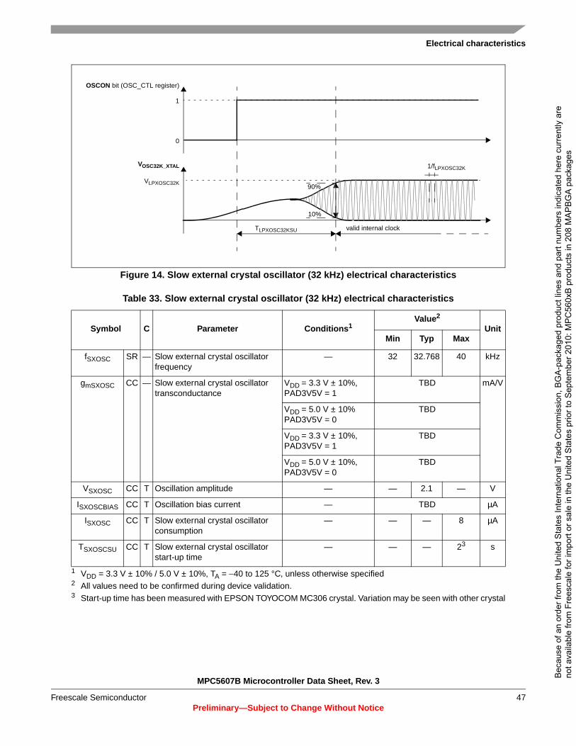
Electrical characteristics
MPC5607B Microcontroller Data Sheet, Rev. 3
Preliminary—Subject to Change Without NoticeFreescale Semiconductor 47
Figure 14. Slow external crystal oscillator (32 kHz) electrical characteristics
Table 33. Slow external crystal oscillator (32 kHz) electrical characteristics
Symbol C Parameter Conditions1
1 VDD = 3.3 V ± 10% / 5.0 V ± 10%, TA = −40 to 125 °C, unless otherwise specified
Value2
2 All values need to be confirmed during device validation.
UnitMin Typ Max
fSXOSC SR — Slow external crystal oscillator frequency
— 32 32.768 40 kHz
gmSXOSC CC — Slow external crystal oscillator transconductance
VDD = 3.3 V ± 10%,PAD3V5V = 1
TBD mA/V
VDD = 5.0 V ± 10%PAD3V5V = 0
TBD
VDD = 3.3 V ± 10%,PAD3V5V = 1
TBD
VDD = 5.0 V ± 10%,PAD3V5V = 0
TBD
VSXOSC CC T Oscillation amplitude — — 2.1 — V
ISXOSCBIAS CC T Oscillation bias current — TBD µA
ISXOSC CC T Slow external crystal oscillator consumption
— — — 8 µA
TSXOSCSU CC T Slow external crystal oscillator start-up time
— — — 23
3 Start-up time has been measured with EPSON TOYOCOM MC306 crystal. Variation may be seen with other crystal
s
OSCON bit (OSC_CTL register)
TLPXOSC32KSU
1
VOSC32K_XTAL
VLPXOSC32K
valid internal clock
90%
10%
1/fLPXOSC32K
0
Bec
ause
of a
n or
der f
rom
the
Uni
ted
Sta
tes
Inte
rnat
iona
l Tra
de C
omm
issi
on, B
GA
-pac
kage
d pr
oduc
t lin
es a
nd p
art n
umbe
rs in
dica
ted
here
cur
rent
ly a
re
not a
vaila
ble
from
Fre
esca
le fo
r im
port
or s
ale
in th
e U
nite
d S
tate
s pr
ior t
o S
epte
mbe
r 201
0: M
PC
560x
B p
rodu
cts
in 2
08 M
AP
BG
A p
acka
ges
MPC5607B Microcontroller Data Sheet, Rev. 3
Preliminary—Subject to Change Without Notice
Electrical characteristics
Freescale Semiconductor48
3.14 FMPLL electrical characteristicsThe device provides a frequency modulated phase locked loop (FMPLL) module to generate a fast system clock from the main oscillator driver.
3.15 Fast internal RC oscillator (16 MHz) electrical characteristicsThe device provides a 16 MHz main internal RC oscillator. This is used as the default clock at the power-up of the device.
Table 34. FMPLL electrical characteristics
Symbol C Parameter Conditions1
1 VDD = 3.3 V ± 10% / 5.0 V ± 10%, TA = −40 to 125 °C, unless otherwise specified.
Value2
2 All values need to be confirmed during device validation.
UnitMin Typ Max
fPLLIN SR — FMPLL reference clock3
3 PLLIN clock retrieved directly from FXOSC clock. Input characteristics are granted when oscillator is used in functional mode. When bypass mode is used, oscillator input clock should verify fPLLIN and ΔPLLIN.
— 4 — 64 MHz
ΔPLLIN SR — FMPLL reference clock duty cycle3
— 40 — 60 %
fPLLOUT CC P FMPLL output clock frequency — 16 — 64 MHz
fCPU SR — System clock frequency — — — 644
4 fCPU 64 MHz can be achieved only at up to 105 °C
MHz
fFREE CC P Free-running frequency — 20 — 150 MHz
tLOCK CC P FMPLL lock time Stable oscillator (fPLLIN = 16 MHz) 40 100 µs
ΔtLTJIT CC — FMPLL long term jitter fPLLIN = 16 MHz (resonator), fPLLCLK @ 64 MHz, 4000 cycles
— — 10 ns
IPLL CC C FMPLL consumption TA = 25 °C — — 4 mA
Table 35. Fast internal RC oscillator (16 MHz) electrical characteristics
Symbol C Parameter Conditions1Value2
UnitMin Typ Max
fFIRC CC P Fast internal RC oscillator high frequency
TA = 25 °C, trimmed — 16 — MHz
SR — — 12 20
IFIRCRUN3, CC T Fast internal RC oscillator high
frequency current in running mode
TA = 25 °C, trimmed — — 200 µA
IFIRCPWD CC D Fast internal RC oscillator high frequency current in power down mode
TA = 25 °C — TBD 10 µA
— TA = 55 °C — TBD TBD
Bec
ause
of a
n or
der f
rom
the
Uni
ted
Sta
tes
Inte
rnat
iona
l Tra
de C
omm
issi
on, B
GA
-pac
kage
d pr
oduc
t lin
es a
nd p
art n
umbe
rs in
dica
ted
here
cur
rent
ly a
re
not a
vaila
ble
from
Fre
esca
le fo
r im
port
or s
ale
in th
e U
nite
d S
tate
s pr
ior t
o S
epte
mbe
r 201
0: M
PC
560x
B p
rodu
cts
in 2
08 M
AP
BG
A p
acka
ges

Electrical characteristics
MPC5607B Microcontroller Data Sheet, Rev. 3
Preliminary—Subject to Change Without NoticeFreescale Semiconductor 49
3.16 Slow internal RC oscillator (128 kHz) electrical characteristicsThe device provides a 128 kHz low power internal RC oscillator. This can be used as the reference clock for the RTC module.
IFIRCSTOP CC T Fast internal RC oscillator high frequency and system clock current in stop mode
TA = 25 °C sysclk = off — 500 — µA
sysclk = 2 MHz — 600 —
sysclk = 4 MHz — 700 —
sysclk = 8 MHz — 900 —
sysclk = 16 MHz — 1250 —
TFIRCSU CC C Fast internal RC oscillator start-up time
TA = 55 °C VDD = 5.0 V ± 10% — 1.1 2.0 µs
— VDD = 3.3 V ± 10% — 1.2 TBD
— TA = 125 °C VDD = 5.0 V ± 10% — — 2.0
— VDD = 3.3 V ± 10% — — TBD
ΔFIRCPRE CC C Fast internal RC oscillator precision after software trimming of fFIRC
TA = 25 °C −1 — +1 %
ΔFIRCTRIM CC C Fast internal RC oscillator trimming step
TA = 25 °C — 1.6 %
ΔFIRCVAR CC C Fast internal RC oscillator variation over temperature and supply with respect to fFIRC at TA = 25 °C in high-frequency configuration
— −5 — +5 %
1 VDD = 3.3 V ± 10% / 5.0 V ± 10%, TA = −40 to 125 °C, unless otherwise specified.2 All values need to be confirmed during device validation.3 This does not include consumption linked to clock tree toggling and peripherals consumption when RC oscillator is
ON.
Table 36. Slow internal RC oscillator (128 kHz) electrical characteristics
Symbol C Parameter Conditions1Value2
UnitMin Typ Max
fSIRC CC P Slow internal RC oscillator low frequency
TA = 25 °C, trimmed — 128 — kHz
SR — — 100 — 150
ISIRC3, CC C Slow internal RC oscillator low
frequency currentTA = 25 °C, trimmed — — 5 µA
Table 35. Fast internal RC oscillator (16 MHz) electrical characteristics (continued)
Symbol C Parameter Conditions1Value2
UnitMin Typ Max
Bec
ause
of a
n or
der f
rom
the
Uni
ted
Sta
tes
Inte
rnat
iona
l Tra
de C
omm
issi
on, B
GA
-pac
kage
d pr
oduc
t lin
es a
nd p
art n
umbe
rs in
dica
ted
here
cur
rent
ly a
re
not a
vaila
ble
from
Fre
esca
le fo
r im
port
or s
ale
in th
e U
nite
d S
tate
s pr
ior t
o S
epte
mbe
r 201
0: M
PC
560x
B p
rodu
cts
in 2
08 M
AP
BG
A p
acka
ges

MPC5607B Microcontroller Data Sheet, Rev. 3
Preliminary—Subject to Change Without Notice
Electrical characteristics
Freescale Semiconductor50
3.17 ADC electrical characteristics
3.17.1 IntroductionThe device provides two Successive Approximation Register (SAR) analog-to-digital converters (10-bit and 12-bit).
TSIRCSU CC P Slow internal RC oscillator start-up time
TA = 25 °C, VDD = 5.0 V ± 10% — 8 12 µs
ΔSIRCPRE CC C Slow internal RC oscillator precision after software trimming of fSIRC
TA = 25 °C −2 — +2 %
ΔSIRCTRIM CC C Slow internal RC oscillator trimming step
— — 2.7 —
ΔSIRCVAR CC C Slow internal RC oscillator variation in temperature and supply with respect to fSIRC at TA = 55 °C in high frequency configuration
High frequency configuration −10 — +10 %
1 VDD = 3.3 V ± 10% / 5.0 V ± 10%, TA = −40 to 125 °C, unless otherwise specified.2 All values need to be confirmed during device validation.3 This does not include consumption linked to clock tree toggling and peripherals consumption when RC oscillator is
ON.
Table 36. Slow internal RC oscillator (128 kHz) electrical characteristics (continued)
Symbol C Parameter Conditions1Value2
UnitMin Typ Max
Bec
ause
of a
n or
der f
rom
the
Uni
ted
Sta
tes
Inte
rnat
iona
l Tra
de C
omm
issi
on, B
GA
-pac
kage
d pr
oduc
t lin
es a
nd p
art n
umbe
rs in
dica
ted
here
cur
rent
ly a
re
not a
vaila
ble
from
Fre
esca
le fo
r im
port
or s
ale
in th
e U
nite
d S
tate
s pr
ior t
o S
epte
mbe
r 201
0: M
PC
560x
B p
rodu
cts
in 2
08 M
AP
BG
A p
acka
ges

Electrical characteristics
MPC5607B Microcontroller Data Sheet, Rev. 3
Preliminary—Subject to Change Without NoticeFreescale Semiconductor 51
Figure 15. ADC0 characteristic and error definitions
3.17.2 Input impedance and ADC accuracyIn the following analysis, the input circuit corresponding to the precise channels is considered.
To preserve the accuracy of the A/D converter, it is necessary that analog input pins have low AC impedance. Placing a capacitor with good high frequency characteristics at the input pin of the device can be effective: the capacitor should be as large as possible, ideally infinite. This capacitor contributes to attenuating the noise present on the input pin; furthermore, it sources charge during the sampling phase, when the analog signal source is a high-impedance source.
A real filter can typically be obtained by using a series resistance with a capacitor on the input pin (simple RC filter). The RC filtering may be limited according to the value of source impedance of the transducer or circuit supplying the analog signal to be measured. The filter at the input pins must be designed taking into account the dynamic characteristics of the input signal (bandwidth) and the equivalent input impedance of the ADC itself.
(2)
(1)
(3)
(4)
(5)
Offset Error OSE
Offset Error OSE
Gain Error GE
1 LSB (ideal)
Vin(A) (LSBideal)
(1) Example of an actual transfer curve
(2) The ideal transfer curve
(3) Differential non-linearity error (DNL)
(4) Integral non-linearity error (INL)
(5) Center of a step of the actual transfer curve
code out
1023
1022
1021
1020
1019
1018
5
4
3
2
1
0
7
6
1 2 3 4 5 6 7 1017 1018 1019 1020 1021 1022 1023
1 LSB ideal = VDD_ADC / 1024
Bec
ause
of a
n or
der f
rom
the
Uni
ted
Sta
tes
Inte
rnat
iona
l Tra
de C
omm
issi
on, B
GA
-pac
kage
d pr
oduc
t lin
es a
nd p
art n
umbe
rs in
dica
ted
here
cur
rent
ly a
re
not a
vaila
ble
from
Fre
esca
le fo
r im
port
or s
ale
in th
e U
nite
d S
tate
s pr
ior t
o S
epte
mbe
r 201
0: M
PC
560x
B p
rodu
cts
in 2
08 M
AP
BG
A p
acka
ges
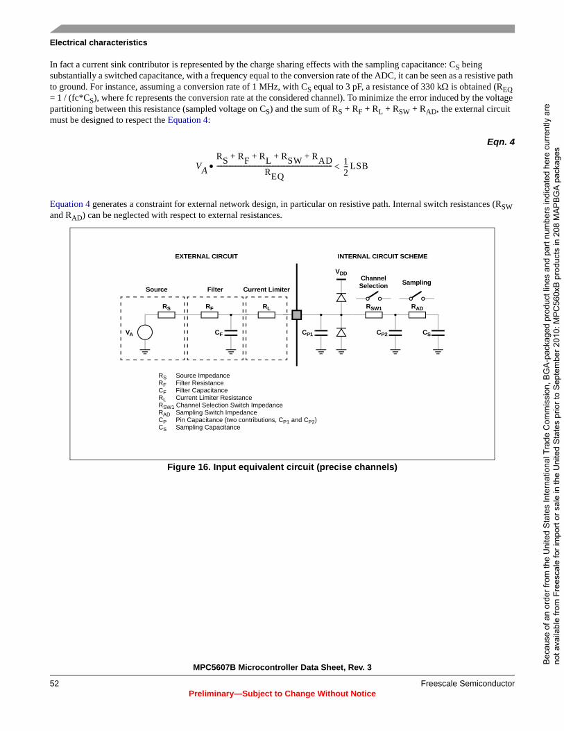
MPC5607B Microcontroller Data Sheet, Rev. 3
Preliminary—Subject to Change Without Notice
Electrical characteristics
Freescale Semiconductor52
In fact a current sink contributor is represented by the charge sharing effects with the sampling capacitance: CS being substantially a switched capacitance, with a frequency equal to the conversion rate of the ADC, it can be seen as a resistive path to ground. For instance, assuming a conversion rate of 1 MHz, with CS equal to 3 pF, a resistance of 330 kΩ is obtained (REQ = 1 / (fc*CS), where fc represents the conversion rate at the considered channel). To minimize the error induced by the voltage partitioning between this resistance (sampled voltage on CS) and the sum of RS + RF + RL + RSW + RAD, the external circuit must be designed to respect the Equation 4:
Eqn. 4
Equation 4 generates a constraint for external network design, in particular on resistive path. Internal switch resistances (RSW and RAD) can be neglected with respect to external resistances.
Figure 16. Input equivalent circuit (precise channels)
VARS RF RL RSW RAD+ + + +
REQ---------------------------------------------------------------------------• 1
2--- LSB<
RF
CF
RS RL RSW1
CP2 CS
VDD
SamplingSource Filter Current Limiter
EXTERNAL CIRCUIT INTERNAL CIRCUIT SCHEME
RS Source ImpedanceRF Filter ResistanceCF Filter CapacitanceRL Current Limiter ResistanceRSW1 Channel Selection Switch ImpedanceRAD Sampling Switch ImpedanceCP Pin Capacitance (two contributions, CP1 and CP2)CS Sampling Capacitance
CP1
RAD
ChannelSelection
VA
Bec
ause
of a
n or
der f
rom
the
Uni
ted
Sta
tes
Inte
rnat
iona
l Tra
de C
omm
issi
on, B
GA
-pac
kage
d pr
oduc
t lin
es a
nd p
art n
umbe
rs in
dica
ted
here
cur
rent
ly a
re
not a
vaila
ble
from
Fre
esca
le fo
r im
port
or s
ale
in th
e U
nite
d S
tate
s pr
ior t
o S
epte
mbe
r 201
0: M
PC
560x
B p
rodu
cts
in 2
08 M
AP
BG
A p
acka
ges

Electrical characteristics
MPC5607B Microcontroller Data Sheet, Rev. 3
Preliminary—Subject to Change Without NoticeFreescale Semiconductor 53
Figure 17. Input equivalent circuit (extended channels)
A second aspect involving the capacitance network shall be considered. Assuming the three capacitances CF, CP1 and CP2 are initially charged at the source voltage VA (refer to the equivalent circuit reported in Figure 16): A charge sharing phenomenon is installed when the sampling phase is started (A/D switch close).
Figure 18. Transient behavior during sampling phase
In particular two different transient periods can be distinguished:1. A first and quick charge transfer from the internal capacitance CP1 and CP2 to the sampling capacitance CS occurs (CS
is supposed initially completely discharged): considering a worst case (since the time constant in reality would be faster) in which CP2 is reported in parallel to CP1 (call CP = CP1 + CP2), the two capacitances CP and CS are in series, and the time constant is
RF
CF
RS RL RSW1
CP3 CS
VDD
SamplingSource Filter Current Limiter
EXTERNAL CIRCUIT INTERNAL CIRCUIT SCHEME
RS Source ImpedanceRF Filter ResistanceCF Filter CapacitanceRL Current Limiter ResistanceRSW Channel Selection Switch Impedance (two contributions RSW1 and RSW2)RAD Sampling Switch ImpedanceCP Pin Capacitance (three contributions, CP1, CP2 and CP3)CS Sampling Capacitance
CP1
RAD
ChannelSelection
VA CP2
Extended
RSW2
Switch
VA
VA1
VA2
tTS
VCS Voltage Transient on CS
ΔV < 0.5 LSB
1 2
τ1 < (RSW + RAD) CS << TS
τ2 = RL (CS + CP1 + CP2)
Bec
ause
of a
n or
der f
rom
the
Uni
ted
Sta
tes
Inte
rnat
iona
l Tra
de C
omm
issi
on, B
GA
-pac
kage
d pr
oduc
t lin
es a
nd p
art n
umbe
rs in
dica
ted
here
cur
rent
ly a
re
not a
vaila
ble
from
Fre
esca
le fo
r im
port
or s
ale
in th
e U
nite
d S
tate
s pr
ior t
o S
epte
mbe
r 201
0: M
PC
560x
B p
rodu
cts
in 2
08 M
AP
BG
A p
acka
ges

MPC5607B Microcontroller Data Sheet, Rev. 3
Preliminary—Subject to Change Without Notice
Electrical characteristics
Freescale Semiconductor54
Eqn. 5
Equation 5 can again be simplified considering only CS as an additional worst condition. In reality, the transient is faster, but the A/D converter circuitry has been designed to be robust also in the very worst case: the sampling time TS is always much longer than the internal time constant:
Eqn. 6
The charge of CP1 and CP2 is redistributed also on CS, determining a new value of the voltage VA1 on the capacitance according to Equation 7:
Eqn. 7
2. A second charge transfer involves also CF (that is typically bigger than the on-chip capacitance) through the resistance RL: again considering the worst case in which CP2 and CS were in parallel to CP1 (since the time constant in reality would be faster), the time constant is:
Eqn. 8
In this case, the time constant depends on the external circuit: in particular imposing that the transient is completed well before the end of sampling time TS, a constraints on RL sizing is obtained:
Eqn. 9
Of course, RL shall be sized also according to the current limitation constraints, in combination with RS (source impedance) and RF (filter resistance). Being CF definitively bigger than CP1, CP2 and CS, then the final voltage VA2 (at the end of the charge transfer transient) will be much higher than VA1. Equation 10 must be respected (charge balance assuming now CS already charged at VA1):
Eqn. 10
The two transients above are not influenced by the voltage source that, due to the presence of the RFCF filter, is not able to provide the extra charge to compensate the voltage drop on CS with respect to the ideal source VA; the time constant RFCF of the filter is very high with respect to the sampling time (TS). The filter is typically designed to act as anti-aliasing.
τ1 RSW RAD+( )=CP CS•
CP CS+---------------------•
τ1 RSW RAD+( )< CS TS«•
VA1 CS CP1 CP2+ +( )• VA CP1 CP2+( )•=
τ2 RL< CS CP1 CP2+ +( )•
10 τ2• 10 RL CS CP1 CP2+ +( )••= TS<
VA2 CS CP1 CP2 CF+ + +( )• VA CF• VA1+ CP1 CP2+ CS+( )•=
Bec
ause
of a
n or
der f
rom
the
Uni
ted
Sta
tes
Inte
rnat
iona
l Tra
de C
omm
issi
on, B
GA
-pac
kage
d pr
oduc
t lin
es a
nd p
art n
umbe
rs in
dica
ted
here
cur
rent
ly a
re
not a
vaila
ble
from
Fre
esca
le fo
r im
port
or s
ale
in th
e U
nite
d S
tate
s pr
ior t
o S
epte
mbe
r 201
0: M
PC
560x
B p
rodu
cts
in 2
08 M
AP
BG
A p
acka
ges
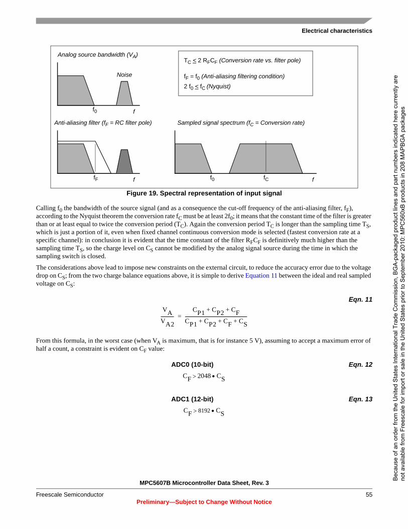
Electrical characteristics
MPC5607B Microcontroller Data Sheet, Rev. 3
Preliminary—Subject to Change Without NoticeFreescale Semiconductor 55
Figure 19. Spectral representation of input signal
Calling f0 the bandwidth of the source signal (and as a consequence the cut-off frequency of the anti-aliasing filter, fF), according to the Nyquist theorem the conversion rate fC must be at least 2f0; it means that the constant time of the filter is greater than or at least equal to twice the conversion period (TC). Again the conversion period TC is longer than the sampling time TS, which is just a portion of it, even when fixed channel continuous conversion mode is selected (fastest conversion rate at a specific channel): in conclusion it is evident that the time constant of the filter RFCF is definitively much higher than the sampling time TS, so the charge level on CS cannot be modified by the analog signal source during the time in which the sampling switch is closed.
The considerations above lead to impose new constraints on the external circuit, to reduce the accuracy error due to the voltage drop on CS; from the two charge balance equations above, it is simple to derive Equation 11 between the ideal and real sampled voltage on CS:
Eqn. 11
From this formula, in the worst case (when VA is maximum, that is for instance 5 V), assuming to accept a maximum error of half a count, a constraint is evident on CF value:
ADC0 (10-bit) Eqn. 12
ADC1 (12-bit) Eqn. 13
f0 f
Analog source bandwidth (VA)
f0 f
Sampled signal spectrum (fC = Conversion rate)
fCf
Anti-aliasing filter (fF = RC filter pole)
fF
2 f0 < fC (Nyquist)
fF = f0 (Anti-aliasing filtering condition)
TC < 2 RFCF (Conversion rate vs. filter pole)
Noise
VAVA2------------
CP1 CP2+ CF+
CP1 CP2+ CF CS+ +--------------------------------------------------------=
CF 2048 CS•>
CF 8192 CS•>
Bec
ause
of a
n or
der f
rom
the
Uni
ted
Sta
tes
Inte
rnat
iona
l Tra
de C
omm
issi
on, B
GA
-pac
kage
d pr
oduc
t lin
es a
nd p
art n
umbe
rs in
dica
ted
here
cur
rent
ly a
re
not a
vaila
ble
from
Fre
esca
le fo
r im
port
or s
ale
in th
e U
nite
d S
tate
s pr
ior t
o S
epte
mbe
r 201
0: M
PC
560x
B p
rodu
cts
in 2
08 M
AP
BG
A p
acka
ges

MPC5607B Microcontroller Data Sheet, Rev. 3
Preliminary—Subject to Change Without Notice
Electrical characteristics
Freescale Semiconductor56
3.17.3 ADC electrical characteristics
Table 37. ADC input leakage current
Symbol C Parameter ConditionsValue
UnitMin Typ Max
ILKG CC C Input leakage current TA = −40 °C No current injection on adjacent pin — 1 — nA
C TA = 25 °C — 1 —
C TA = 105 °C — 8 200
P TA = 125 °C — 45 400
Table 38. ADC conversion characteristics (10-bit ADC0)
Symbol CParamete
rConditions1
ValueUnit
Min Typ Max
VSS_ADC0 SR — Voltage on VSS_HV_ADC0 (ADC0 reference) pin with respect to ground (VSS)2
— −0.1 — 0.1 V
VDD_ADC0 SR — Voltage on VDD_HV_ADC pin (ADC reference) with respect to ground (VSS)
— VDD−0.1 — VDD+0.1 V
VAINx SR — Analog input voltage3
— VSS_ADC0−0.1
— VDD_ADC0+0.1
V
fADC0 SR — ADC0 analog frequency
— 6 — 32 + 4% MHz
ΔADC0_SY
S
SR — ADC0 digital clock duty cycle (ipg_clk)
ADCLKSEL = 14 45 — 55 %
tADC0_PU SR — ADC0 power up delay
— — — 1.5 µs
Bec
ause
of a
n or
der f
rom
the
Uni
ted
Sta
tes
Inte
rnat
iona
l Tra
de C
omm
issi
on, B
GA
-pac
kage
d pr
oduc
t lin
es a
nd p
art n
umbe
rs in
dica
ted
here
cur
rent
ly a
re
not a
vaila
ble
from
Fre
esca
le fo
r im
port
or s
ale
in th
e U
nite
d S
tate
s pr
ior t
o S
epte
mbe
r 201
0: M
PC
560x
B p
rodu
cts
in 2
08 M
AP
BG
A p
acka
ges

Electrical characteristics
MPC5607B Microcontroller Data Sheet, Rev. 3
Preliminary—Subject to Change Without NoticeFreescale Semiconductor 57
tADC0_S CC T Sample time5
fADC = 32 MHz,ADC0_conf_sample_input = 17
0.5 — µs
fADC = 6 MHz,INPSAMP = 255
— 42
tADC0_C CC P Conversion time6
fADC = 32 MHz,ADC_conf_comp = 2
0.625 — µs
CS CC D ADC0 input sampling capacitance
— — — 3 pF
CP1 CC D ADC0 input pin capacitance 1
— — — 3 pF
CP2 CC D ADC0 input pin capacitance 2
— — — 1 pF
CP3 CC D ADC0 input pin capacitance 3
— — — 1 pF
RSW1 CC D Internal resistance of analog source
— — — 3 kΩ
RSW2 CC D Internal resistance of analog source
— — — 2 kΩ
RAD CC D Internal resistance of analog source
— — — 2 kΩ
IINJ SR — Input current Injection
Current injection on one ADC0 input, different from the converted one
VDD = 3.3 V ± 10%
−5 — 5 mA
VDD = 5.0 V ± 10%
−5 — 5
Table 38. ADC conversion characteristics (continued)(10-bit ADC0)
Symbol CParamete
rConditions1
ValueUnit
Min Typ Max
Bec
ause
of a
n or
der f
rom
the
Uni
ted
Sta
tes
Inte
rnat
iona
l Tra
de C
omm
issi
on, B
GA
-pac
kage
d pr
oduc
t lin
es a
nd p
art n
umbe
rs in
dica
ted
here
cur
rent
ly a
re
not a
vaila
ble
from
Fre
esca
le fo
r im
port
or s
ale
in th
e U
nite
d S
tate
s pr
ior t
o S
epte
mbe
r 201
0: M
PC
560x
B p
rodu
cts
in 2
08 M
AP
BG
A p
acka
ges

MPC5607B Microcontroller Data Sheet, Rev. 3
Preliminary—Subject to Change Without Notice
Electrical characteristics
Freescale Semiconductor58
| INL | CC T Absolute value for integral non-linearity
No overload — 0.5 1.5 LSB
| DNL | CC T Absolute differential non-linearity
No overload — 0.5 1.0 LSB
| OFS | CC T Absolute offset error
— — 0.5 — LSB
| GNE | CC T Absolute gain error
— — 0.6 — LSB
TUEP CC P Total unadjusted error7 for precise channels, input only pins
Without current injection
−2 0.6 2 LSB
T With current injection −3 3
TUEX CC T Total unadjusted error7 for extended channel
Without current injection
−3 1 3 LSB
T With current injection −4 4
1 VDD = 3.3 V ± 10% / 5.0 V ± 10%, TA = −40 to 125 °C, unless otherwise specified.2 Analog and digital VSS must be common (to be tied together externally).3 VAINx may exceed VSS_ADC0 and VDD_ADC0 limits, remaining on absolute maximum ratings, but the results of the
conversion will be clamped respectively to 0x000 or 0x3FF.4 Duty cycle is ensured by using system clock without prescaling. When ADCLKSEL = 0, the duty cycle is ensured
by internal divider by 2.5 During the sample time the input capacitance CS can be charged/discharged by the external source. The internal
resistance of the analog source must allow the capacitance to reach its final voltage level within tADC0_S. After the end of the sample time tADC0_S, changes of the analog input voltage have no effect on the conversion result. Values for the sample clock tADC0_S depend on programming.
6 This parameter does not include the sample time tADC0_S, but only the time for determining the digital result and the time to load the result’s register with the conversion result.
7 Total Unadjusted Error: The maximum error that occurs without adjusting Offset and Gain errors. This error is a combination of Offset, Gain and Integral Linearity errors.
Table 38. ADC conversion characteristics (continued)(10-bit ADC0)
Symbol CParamete
rConditions1
ValueUnit
Min Typ Max
Bec
ause
of a
n or
der f
rom
the
Uni
ted
Sta
tes
Inte
rnat
iona
l Tra
de C
omm
issi
on, B
GA
-pac
kage
d pr
oduc
t lin
es a
nd p
art n
umbe
rs in
dica
ted
here
cur
rent
ly a
re
not a
vaila
ble
from
Fre
esca
le fo
r im
port
or s
ale
in th
e U
nite
d S
tate
s pr
ior t
o S
epte
mbe
r 201
0: M
PC
560x
B p
rodu
cts
in 2
08 M
AP
BG
A p
acka
ges

Electrical characteristics
MPC5607B Microcontroller Data Sheet, Rev. 3
Preliminary—Subject to Change Without NoticeFreescale Semiconductor 59
Figure 20. ADC1 characteristic and error definitions
(2)
(1)
(3)
(4)
(5)
Offset Error OSE
Offset Error OSE
Gain Error GE
1 LSB (ideal)
Vin(A) (LSBideal)
(1) Example of an actual transfer curve
(2) The ideal transfer curve
(3) Differential non-linearity error (DNL)
(4) Integral non-linearity error (INL)
(5) Center of a step of the actual transfer curve
code out
4095
4094
4093
4092
4091
4090
5
4
3
2
1
0
7
6
1 2 3 4 5 6 7 4090 4091 4092 4093 4094 4095
1 LSB ideal = AVDD / 4096
Bec
ause
of a
n or
der f
rom
the
Uni
ted
Sta
tes
Inte
rnat
iona
l Tra
de C
omm
issi
on, B
GA
-pac
kage
d pr
oduc
t lin
es a
nd p
art n
umbe
rs in
dica
ted
here
cur
rent
ly a
re
not a
vaila
ble
from
Fre
esca
le fo
r im
port
or s
ale
in th
e U
nite
d S
tate
s pr
ior t
o S
epte
mbe
r 201
0: M
PC
560x
B p
rodu
cts
in 2
08 M
AP
BG
A p
acka
ges

MPC5607B Microcontroller Data Sheet, Rev. 3
Preliminary—Subject to Change Without Notice
Electrical characteristics
Freescale Semiconductor60
Table 39. Conversion characteristics (12-bit ADC1)
Symbol Parameter Conditions1Value
UnitMin Typ Max
VSS_ADC1 SR Voltage on VSS_HV_ADC1 (ADC1 reference) pin with respect to ground (VSS)2
— -0.1 0.1 V
VDD_ADC1 SR Voltage on VDD_HV_ADC1 pin (ADC1 reference) with respect to ground (VSS)
— VDD-0.1 VDD+0.1 V
VAINx SR Analog input voltage3
— VSS_ADC1-0.1
VDD_ADC1+0.1
V
fADC1 SR ADC1 analog frequency
— 32 + 3% 32 + 4% MHz
tADC1_PU SR ADC1 power up delay
— 1.5 µs
tADC1_S CC Sample time4
VDD=3.3 V
fADC1= 32 MHz,ADC1_conf_sample_input = 20
600 ns
Sample time4
VDD =5.0 V
fADC1= 32 MHz,ADC1_conf_sample_input = 17
500
Sample time4
VDD=3.3 V
fADC1= 3.33 MHz,ADC1_conf_sample_input = 255
76.2 µs
Sample time4
VDD =5.0 V
fADC1= 3.33 MHz,ADC1_conf_sample_input = 255
76.2
Bec
ause
of a
n or
der f
rom
the
Uni
ted
Sta
tes
Inte
rnat
iona
l Tra
de C
omm
issi
on, B
GA
-pac
kage
d pr
oduc
t lin
es a
nd p
art n
umbe
rs in
dica
ted
here
cur
rent
ly a
re
not a
vaila
ble
from
Fre
esca
le fo
r im
port
or s
ale
in th
e U
nite
d S
tate
s pr
ior t
o S
epte
mbe
r 201
0: M
PC
560x
B p
rodu
cts
in 2
08 M
AP
BG
A p
acka
ges

Electrical characteristics
MPC5607B Microcontroller Data Sheet, Rev. 3
Preliminary—Subject to Change Without NoticeFreescale Semiconductor 61
tADC1_C CC Conversion time5
VDD=3.3 V
fADC1 = 20MHz,ADC1_conf_comp = 0
2.4 µs
Conversion time5
VDD =5.0 V
fADC 1= 13.33 MHz,ADC1_conf_comp = 0
1.5 µs
Conversion time5
VDD=3.3 V
fADC 1= 13.33 MHz,ADC1_conf_comp = 0
3.6 µs
Conversion time5
VDD =5.0 V
fADC1 = 32 MHz,ADC1_conf_comp = 0
3.6 µs
ΔADC0_SYS SR ADC1 digital clock duty cycle (ipg_clk)
ADCLKSEL = 16 45 — 55 %
CS CC ADC1 input sampling capacitance
— 5 pF
CP1 CC ADC1 input pin capacitance 1
— 3 pF
CP2 CC ADC1 input pin capacitance 2
— 1 pF
CP3 CC ADC1 input pin capacitance 3
— 1.5 pF
RSW1 CC Internal resistance of analog source
— 1 kΩ
RSW2 CC Internal resistance of analog source
— 2 kΩ
RAD CC Internal resistance of analog source
— 0.3 kΩ
Table 39. Conversion characteristics (12-bit ADC1) (continued)
Symbol Parameter Conditions1Value
UnitMin Typ Max
Bec
ause
of a
n or
der f
rom
the
Uni
ted
Sta
tes
Inte
rnat
iona
l Tra
de C
omm
issi
on, B
GA
-pac
kage
d pr
oduc
t lin
es a
nd p
art n
umbe
rs in
dica
ted
here
cur
rent
ly a
re
not a
vaila
ble
from
Fre
esca
le fo
r im
port
or s
ale
in th
e U
nite
d S
tate
s pr
ior t
o S
epte
mbe
r 201
0: M
PC
560x
B p
rodu
cts
in 2
08 M
AP
BG
A p
acka
ges

MPC5607B Microcontroller Data Sheet, Rev. 3
Preliminary—Subject to Change Without Notice
Electrical characteristics
Freescale Semiconductor62
IINJ SR Input current Injection
Current injection on one ADC1 input, different from the converted one
VDD = 3.3 V ± 10%
-5 — 5 mA
VDD = 5.0 V ± 10%
-5 — 5
INLP CC Absolute Integral non-linearity-Precise channels
No overload 1 3 LSB
INLX CC Absolute Integral non-linearity-Extended channels
No overload 1.5 5 LSB
DNL CC Absolute Differential non-linearity
No overload 0.5 1 LSB
OFS CC Absolute Offset error
— 2 LSB
GNE CC Absolute Gain error
— 2 LSB
TUEP7 CC Total Unadjusted Error for precise channels, input only pins
Without current injection -6 6
With current injection -8 8
TUEX7 CC Total Unadjusted Error for extended channel
Without current injection -10 10 LSB
With current injection -12 12 LSB
1 VDD = 3.3 V ± 10% / 5.0 V ± 10%, TA = -40 / 125 °C, unless otherwise specified.2 Analog and digital VSS must be common (to be tied together externally).3 VAINx may exceed VSS_ADC1 and VDD_ADC1 limits, remaining on absolute maximum ratings, but the results of the
conversion will be clamped respectively to 0x000 or 0xFFF.4 During the sample time the input capacitance CS can be charged/discharged by the external source. The internal
resistance of the analog source must allow the capacitance to reach its final voltage level within tADC1_S. After the end of the sample time tADC1_S, changes of the analog input voltage have no effect on the conversion result. Values for the sample clock tADC1_S depend on programming.
Table 39. Conversion characteristics (12-bit ADC1) (continued)
Symbol Parameter Conditions1Value
UnitMin Typ Max
Bec
ause
of a
n or
der f
rom
the
Uni
ted
Sta
tes
Inte
rnat
iona
l Tra
de C
omm
issi
on, B
GA
-pac
kage
d pr
oduc
t lin
es a
nd p
art n
umbe
rs in
dica
ted
here
cur
rent
ly a
re
not a
vaila
ble
from
Fre
esca
le fo
r im
port
or s
ale
in th
e U
nite
d S
tate
s pr
ior t
o S
epte
mbe
r 201
0: M
PC
560x
B p
rodu
cts
in 2
08 M
AP
BG
A p
acka
ges

Electrical characteristics
MPC5607B Microcontroller Data Sheet, Rev. 3
Preliminary—Subject to Change Without NoticeFreescale Semiconductor 63
5 This parameter does not include the sample time tADC1_S, but only the time for determining the digital result and the time to load the result’s register with the conversion result.
6 Duty cycle is ensured by using system clock without prescaling. When ADCLKSEL = 0, the duty cycle is ensured by internal divider by 2.
7 Total Unadjusted Error: The maximum error that occurs without adjusting Offset and Gain errors. This error is a combination of Offset, Gain and Integral Linearity errors.
Bec
ause
of a
n or
der f
rom
the
Uni
ted
Sta
tes
Inte
rnat
iona
l Tra
de C
omm
issi
on, B
GA
-pac
kage
d pr
oduc
t lin
es a
nd p
art n
umbe
rs in
dica
ted
here
cur
rent
ly a
re
not a
vaila
ble
from
Fre
esca
le fo
r im
port
or s
ale
in th
e U
nite
d S
tate
s pr
ior t
o S
epte
mbe
r 201
0: M
PC
560x
B p
rodu
cts
in 2
08 M
AP
BG
A p
acka
ges

MPC5607B Microcontroller Data Sheet, Rev. 3
Preliminary—Subject to Change Without Notice
Electrical characteristics
Freescale Semiconductor64
3.18 On-chip peripherals
3.18.1 Current consumptionTable 40. On-chip peripherals current consumption1
Symbol C Parameter ConditionsValue
UnitMin Typ Max
IDD_BV(CAN
) CC T CAN
(FlexCAN) supply current on VDD_BV
500 Kbps Total (static + dynamic) consumption: • FlexCAN
in loop-back mode
• XTAL@8MHz used as CAN engine clock source
• Message sending period is 580 µs
7.652 * fperiph + 84.73 µA
125 Kbps 8.0743 * fperiph + 26.757
IDD_BV(eMI
OS) CC T eMIOS
supply current on VDD_BV
Static consumption: • eMIOS channel OFF • Global prescaler
enabled
28.7 * fperiph
Dynamic consumption: • It does not change
varying the frequency (0.003 mA)
3
IDD_BV(SCI) CC T SCI (LINFlex) supply current on VDD_BV
Total (static + dynamic) consumption: • LIN mode • Baudrate: 20 Kbps
4.7804 * fperiph + 30.946
IDD_BV(SPI) CC T SPI (DSPI) supply current on VDD_BV
Ballast static consumption (only clocked)
1
Ballast dynamic consumption (continuus communication): • Baudrate: 2 Mbit • Trasmission every 8
µs • Frame: 16 bits
16.3 * fperiph
Bec
ause
of a
n or
der f
rom
the
Uni
ted
Sta
tes
Inte
rnat
iona
l Tra
de C
omm
issi
on, B
GA
-pac
kage
d pr
oduc
t lin
es a
nd p
art n
umbe
rs in
dica
ted
here
cur
rent
ly a
re
not a
vaila
ble
from
Fre
esca
le fo
r im
port
or s
ale
in th
e U
nite
d S
tate
s pr
ior t
o S
epte
mbe
r 201
0: M
PC
560x
B p
rodu
cts
in 2
08 M
AP
BG
A p
acka
ges

Electrical characteristics
MPC5607B Microcontroller Data Sheet, Rev. 3
Preliminary—Subject to Change Without NoticeFreescale Semiconductor 65
IDD_BV(ADC
) CC T ADC
supply current on VDD_BV
VDD = 5.5 V
Ballast static
consumption (no
conversion)
0.0409 * fperiph mA
VDD = 5.5 V
Ballast dynamic
consumption
(continuus conversion
)
0.0049 * fperiph
IDD_HV_AD
C(ADC) CC T ADC
supply current on VDD_HV_AD
C
VDD = 5.5 V
Analog static
consumption (no
conversion)
0.0017 * fperiph
VDD = 5.5 V
Analog dynamic
consumption
(continuus conversion
)
0.075 * fperiph + 0.032
IDD_HV(FLA
SH) CC T CFlash +
DFlash supply current on VDD_HV_AD
C
VDD = 5.5 V
- 13.25
IDD_HV(PLL) CC T PLL supply current on VDD_HV
VDD = 5.5 V
- 0.0031 * fperiph
1 Operating conditions: TA = 25 °C, fperiph = 8 MHz to 64 MHz
Table 40. On-chip peripherals current consumption1 (continued)
Symbol C Parameter ConditionsValue
UnitMin Typ Max
Bec
ause
of a
n or
der f
rom
the
Uni
ted
Sta
tes
Inte
rnat
iona
l Tra
de C
omm
issi
on, B
GA
-pac
kage
d pr
oduc
t lin
es a
nd p
art n
umbe
rs in
dica
ted
here
cur
rent
ly a
re
not a
vaila
ble
from
Fre
esca
le fo
r im
port
or s
ale
in th
e U
nite
d S
tate
s pr
ior t
o S
epte
mbe
r 201
0: M
PC
560x
B p
rodu
cts
in 2
08 M
AP
BG
A p
acka
ges
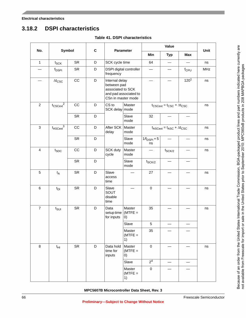
MPC5607B Microcontroller Data Sheet, Rev. 3
Preliminary—Subject to Change Without Notice
Electrical characteristics
Freescale Semiconductor66
3.18.2 DSPI characteristics
Table 41. DSPI characteristics
No. Symbol C ParameterValue
UnitMin Typ Max
1 tSCK SR D SCK cycle time 64 — — ns
— fDSPI SR D DSPI digital controller frequency
— — fCPU MHz
— ΔtCSC CC D Internal delay between pad associated to SCK and pad associated to CSn in master mode
— — 1201 ns
2 tCSCext2 CC D CS to
SCK delayMaster mode
tCSCext = tCSC + ΔtCSC ns
SR D Slave mode
32 — —
3 tASCext3 CC D After SCK
delayMaster mode
tASCext = tASC + ΔtCSC ns
SR D Slave mode
1/fDSPI + 5 ns
— — ns
4 tSDC CC D SCK duty cycle
Master mode
— tSCK/2 — ns
SR D Slave mode
tSCK/2 — —
5 tA SR D Slave access time
— 27 — — ns
6 tDI SR D Slave SOUT disable time
— 0 — — ns
7 tSUI SR D Data setup time for inputs
Master (MTFE = 0)
35 — — ns
Slave 5 — —
Master (MTFE =1)
35 — —
8 tHI SR D Data hold time for inputs
Master (MTFE = 0)
0 — — ns
Slave 24 — —
Master (MTFE =1)
0 — —
Bec
ause
of a
n or
der f
rom
the
Uni
ted
Sta
tes
Inte
rnat
iona
l Tra
de C
omm
issi
on, B
GA
-pac
kage
d pr
oduc
t lin
es a
nd p
art n
umbe
rs in
dica
ted
here
cur
rent
ly a
re
not a
vaila
ble
from
Fre
esca
le fo
r im
port
or s
ale
in th
e U
nite
d S
tate
s pr
ior t
o S
epte
mbe
r 201
0: M
PC
560x
B p
rodu
cts
in 2
08 M
AP
BG
A p
acka
ges
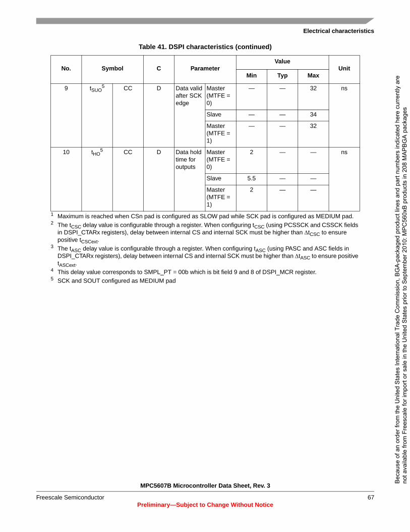
Electrical characteristics
MPC5607B Microcontroller Data Sheet, Rev. 3
Preliminary—Subject to Change Without NoticeFreescale Semiconductor 67
9 tSUO5 CC D Data valid
after SCK edge
Master (MTFE = 0)
— — 32 ns
Slave — — 34
Master (MTFE = 1)
— — 32
10 tHO5 CC D Data hold
time for outputs
Master (MTFE = 0)
2 — — ns
Slave 5.5 — —
Master (MTFE = 1)
2 — —
1 Maximum is reached when CSn pad is configured as SLOW pad while SCK pad is configured as MEDIUM pad.2 The tCSC delay value is configurable through a register. When configuring tCSC (using PCSSCK and CSSCK fields
in DSPI_CTARx registers), delay between internal CS and internal SCK must be higher than ΔtCSC to ensure positive tCSCext.
3 The tASC delay value is configurable through a register. When configuring tASC (using PASC and ASC fields in DSPI_CTARx registers), delay between internal CS and internal SCK must be higher than ΔtASC to ensure positive tASCext.
4 This delay value corresponds to SMPL_PT = 00b which is bit field 9 and 8 of DSPI_MCR register.5 SCK and SOUT configured as MEDIUM pad
Table 41. DSPI characteristics (continued)
No. Symbol C ParameterValue
UnitMin Typ Max
Bec
ause
of a
n or
der f
rom
the
Uni
ted
Sta
tes
Inte
rnat
iona
l Tra
de C
omm
issi
on, B
GA
-pac
kage
d pr
oduc
t lin
es a
nd p
art n
umbe
rs in
dica
ted
here
cur
rent
ly a
re
not a
vaila
ble
from
Fre
esca
le fo
r im
port
or s
ale
in th
e U
nite
d S
tate
s pr
ior t
o S
epte
mbe
r 201
0: M
PC
560x
B p
rodu
cts
in 2
08 M
AP
BG
A p
acka
ges
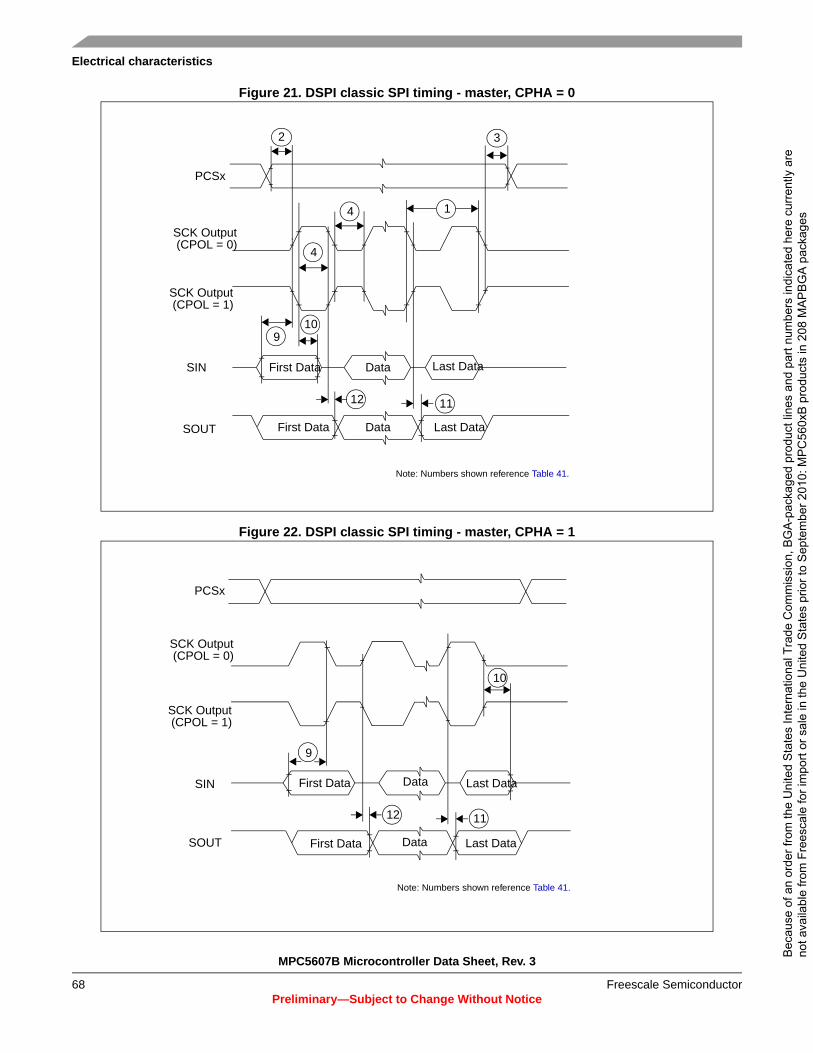
MPC5607B Microcontroller Data Sheet, Rev. 3
Preliminary—Subject to Change Without Notice
Electrical characteristics
Freescale Semiconductor68
Figure 21. DSPI classic SPI timing - master, CPHA = 0
Figure 22. DSPI classic SPI timing - master, CPHA = 1
Data Last DataFirst Data
First Data Data Last Data
SIN
SOUT
PCSx
SCK Output
4
9
12
1
11
10
4
SCK Output
(CPOL = 0)
(CPOL = 1)
32
Note: Numbers shown reference Table 41.
Data Last DataFirst DataSIN
SOUT
12 11
10
Last DataDataFirst Data
SCK Output
SCK Output
PCSx
9
(CPOL = 0)
(CPOL = 1)
Note: Numbers shown reference Table 41.
Bec
ause
of a
n or
der f
rom
the
Uni
ted
Sta
tes
Inte
rnat
iona
l Tra
de C
omm
issi
on, B
GA
-pac
kage
d pr
oduc
t lin
es a
nd p
art n
umbe
rs in
dica
ted
here
cur
rent
ly a
re
not a
vaila
ble
from
Fre
esca
le fo
r im
port
or s
ale
in th
e U
nite
d S
tate
s pr
ior t
o S
epte
mbe
r 201
0: M
PC
560x
B p
rodu
cts
in 2
08 M
AP
BG
A p
acka
ges
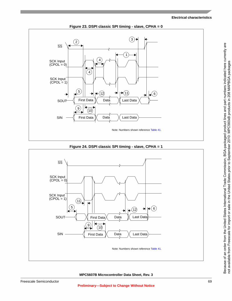
Electrical characteristics
MPC5607B Microcontroller Data Sheet, Rev. 3
Preliminary—Subject to Change Without NoticeFreescale Semiconductor 69
Figure 23. DSPI classic SPI timing - slave, CPHA = 0
Figure 24. DSPI classic SPI timing - slave, CPHA = 1
Last DataFirst Data
3
4
1
Data
Data
SIN
SOUT
SS
4
5 6
9
11
10
12
SCK Input
First Data Last Data
SCK Input
2
(CPOL = 0)
(CPOL = 1)
Note: Numbers shown reference Table 41.
5 6
9
12
11
10
Last Data
Last DataSIN
SOUT
SS
First Data
First Data
Data
Data
SCK Input
SCK Input
(CPOL = 0)
(CPOL = 1)
Note: Numbers shown reference Table 41.
Bec
ause
of a
n or
der f
rom
the
Uni
ted
Sta
tes
Inte
rnat
iona
l Tra
de C
omm
issi
on, B
GA
-pac
kage
d pr
oduc
t lin
es a
nd p
art n
umbe
rs in
dica
ted
here
cur
rent
ly a
re
not a
vaila
ble
from
Fre
esca
le fo
r im
port
or s
ale
in th
e U
nite
d S
tate
s pr
ior t
o S
epte
mbe
r 201
0: M
PC
560x
B p
rodu
cts
in 2
08 M
AP
BG
A p
acka
ges
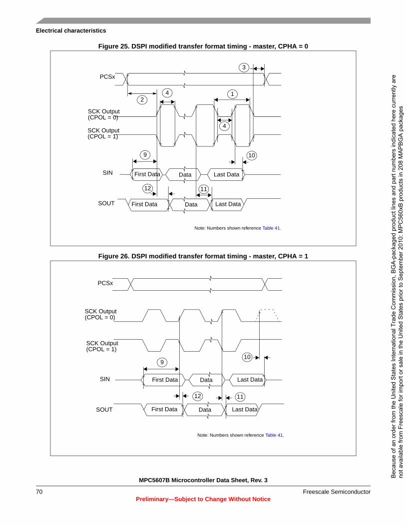
MPC5607B Microcontroller Data Sheet, Rev. 3
Preliminary—Subject to Change Without Notice
Electrical characteristics
Freescale Semiconductor70
Figure 25. DSPI modified transfer format timing - master, CPHA = 0
Figure 26. DSPI modified transfer format timing - master, CPHA = 1
PCSx
3
14
10
4
9
12 11
SCK Output
SCK Output
SIN
SOUT
First Data Data Last Data
First Data Data Last Data
2
(CPOL = 0)
(CPOL = 1)
Note: Numbers shown reference Table 41.
PCSx
109
12 11
SCK Output
SCK Output
SIN
SOUT
First Data Data Last Data
First Data Data Last Data
(CPOL = 0)
(CPOL = 1)
Note: Numbers shown reference Table 41.
Bec
ause
of a
n or
der f
rom
the
Uni
ted
Sta
tes
Inte
rnat
iona
l Tra
de C
omm
issi
on, B
GA
-pac
kage
d pr
oduc
t lin
es a
nd p
art n
umbe
rs in
dica
ted
here
cur
rent
ly a
re
not a
vaila
ble
from
Fre
esca
le fo
r im
port
or s
ale
in th
e U
nite
d S
tate
s pr
ior t
o S
epte
mbe
r 201
0: M
PC
560x
B p
rodu
cts
in 2
08 M
AP
BG
A p
acka
ges

Electrical characteristics
MPC5607B Microcontroller Data Sheet, Rev. 3
Preliminary—Subject to Change Without NoticeFreescale Semiconductor 71
Figure 27. DSPI modified transfer format timing - slave, CPHA = 0
Figure 28. DSPI modified transfer format timing - slave, CPHA = 1
Last DataFirst Data
3
4
1
Data
Data
SIN
SOUT
SS
4
5 6
9
11
10
SCK Input
First Data Last Data
SCK Input
2
(CPOL = 0)
(CPOL = 1)
12
Note: Numbers shown reference Table 41.
5 6
9
12
11
10
Last Data
Last DataSIN
SOUT
SS
First Data
First Data
Data
Data
SCK Input
SCK Input
(CPOL = 0)
(CPOL = 1)
Note: Numbers shown reference Table 41.
Bec
ause
of a
n or
der f
rom
the
Uni
ted
Sta
tes
Inte
rnat
iona
l Tra
de C
omm
issi
on, B
GA
-pac
kage
d pr
oduc
t lin
es a
nd p
art n
umbe
rs in
dica
ted
here
cur
rent
ly a
re
not a
vaila
ble
from
Fre
esca
le fo
r im
port
or s
ale
in th
e U
nite
d S
tate
s pr
ior t
o S
epte
mbe
r 201
0: M
PC
560x
B p
rodu
cts
in 2
08 M
AP
BG
A p
acka
ges

MPC5607B Microcontroller Data Sheet, Rev. 3
Preliminary—Subject to Change Without Notice
Electrical characteristics
Freescale Semiconductor72
Figure 29. DSPI PCS strobe (PCSS) timing
PCSx
7 8
PCSS
Note: Numbers shown reference Table 41.
Bec
ause
of a
n or
der f
rom
the
Uni
ted
Sta
tes
Inte
rnat
iona
l Tra
de C
omm
issi
on, B
GA
-pac
kage
d pr
oduc
t lin
es a
nd p
art n
umbe
rs in
dica
ted
here
cur
rent
ly a
re
not a
vaila
ble
from
Fre
esca
le fo
r im
port
or s
ale
in th
e U
nite
d S
tate
s pr
ior t
o S
epte
mbe
r 201
0: M
PC
560x
B p
rodu
cts
in 2
08 M
AP
BG
A p
acka
ges

Electrical characteristics
MPC5607B Microcontroller Data Sheet, Rev. 3
Preliminary—Subject to Change Without NoticeFreescale Semiconductor 73
3.18.3 Nexus characteristics
Figure 30. Nexus TDI, TMS, TDO timing
Table 42. Nexus characteristics
No. Symbol C ParameterValue
UnitMin Typ Max
1 tTCYC CC D TCK cycle time 64 — — ns
2 tMCYC CC D MCKO cycle time 32 — — ns
3 tMDOV CC D MCKO low to MDO data valid — — 8 ns
4 tMSEOV CC D MCKO low to MSEO_b data valid — — 8 ns
5 tEVTOV CC D MCKO low to EVTO data valid — — 8 ns
6 tNTDIS CC D TDI data setup time 15 — — ns
tNTMSS CC D TMS data setup time 15 — — ns
7 tNTDIH CC D TDI data hold time 5 — — ns
tNTMSH CC D TMS data hold time 5 — — ns
8 tTDOV CC D TCK low to TDO data valid 35 — — ns
9 tTDOI CC D TCK low to TDO data invalid 6 — — ns
10
TCK
TMS, TDI
TDO
11
12
Note: Numbers shown reference Table 42.
Bec
ause
of a
n or
der f
rom
the
Uni
ted
Sta
tes
Inte
rnat
iona
l Tra
de C
omm
issi
on, B
GA
-pac
kage
d pr
oduc
t lin
es a
nd p
art n
umbe
rs in
dica
ted
here
cur
rent
ly a
re
not a
vaila
ble
from
Fre
esca
le fo
r im
port
or s
ale
in th
e U
nite
d S
tate
s pr
ior t
o S
epte
mbe
r 201
0: M
PC
560x
B p
rodu
cts
in 2
08 M
AP
BG
A p
acka
ges

MPC5607B Microcontroller Data Sheet, Rev. 3
Preliminary—Subject to Change Without Notice
Electrical characteristics
Freescale Semiconductor74
3.18.4 JTAG characteristics
Figure 31. Timing diagram - JTAG boundary scan
Table 43. JTAG characteristics
No. Symbol C ParameterValue
UnitMin Typ Max
1 tJCYC CC D TCK cycle time 64 — — ns
2 tTDIS CC D TDI setup time 15 — — ns
3 tTDIH CC D TDI hold time 5 — — ns
4 tTMSS CC D TMS setup time 15 — — ns
5 tTMSH CC D TMS hold time 5 — — ns
6 tTDOV CC D TCK low to TDO valid — 33 ns
7 tTDOI CC D TCK low to TDO invalid 6 — — ns
INPUT DATA VALID
OUTPUT DATA VALID
DATA INPUTS
DATA OUTPUTS
DATA OUTPUTS
TCK
Note: Numbers shown reference Table 43.
3/52/4
7
6
Bec
ause
of a
n or
der f
rom
the
Uni
ted
Sta
tes
Inte
rnat
iona
l Tra
de C
omm
issi
on, B
GA
-pac
kage
d pr
oduc
t lin
es a
nd p
art n
umbe
rs in
dica
ted
here
cur
rent
ly a
re
not a
vaila
ble
from
Fre
esca
le fo
r im
port
or s
ale
in th
e U
nite
d S
tate
s pr
ior t
o S
epte
mbe
r 201
0: M
PC
560x
B p
rodu
cts
in 2
08 M
AP
BG
A p
acka
ges
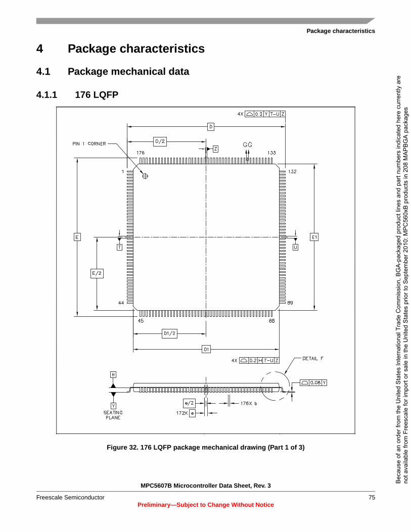
Package characteristics
MPC5607B Microcontroller Data Sheet, Rev. 3
Preliminary—Subject to Change Without NoticeFreescale Semiconductor 75
4 Package characteristics
4.1 Package mechanical data
4.1.1 176 LQFP
Figure 32. 176 LQFP package mechanical drawing (Part 1 of 3)
Bec
ause
of a
n or
der f
rom
the
Uni
ted
Sta
tes
Inte
rnat
iona
l Tra
de C
omm
issi
on, B
GA
-pac
kage
d pr
oduc
t lin
es a
nd p
art n
umbe
rs in
dica
ted
here
cur
rent
ly a
re
not a
vaila
ble
from
Fre
esca
le fo
r im
port
or s
ale
in th
e U
nite
d S
tate
s pr
ior t
o S
epte
mbe
r 201
0: M
PC
560x
B p
rodu
cts
in 2
08 M
AP
BG
A p
acka
ges
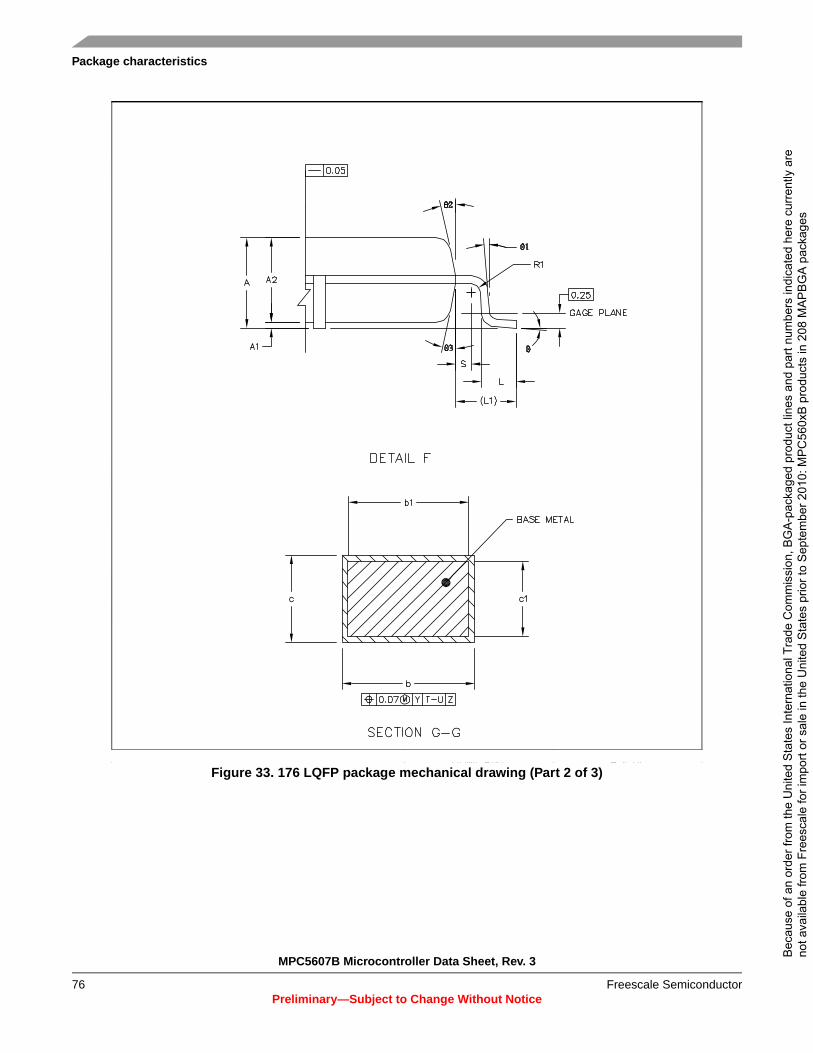
MPC5607B Microcontroller Data Sheet, Rev. 3
Preliminary—Subject to Change Without Notice
Package characteristics
Freescale Semiconductor76
Figure 33. 176 LQFP package mechanical drawing (Part 2 of 3)B
ecau
se o
f an
orde
r fro
m th
e U
nite
d S
tate
s In
tern
atio
nal T
rade
Com
mis
sion
, BG
A-p
acka
ged
prod
uct l
ines
and
par
t num
bers
indi
cate
d he
re c
urre
ntly
are
no
t ava
ilabl
e fro
m F
rees
cale
for i
mpo
rt or
sal
e in
the
Uni
ted
Sta
tes
prio
r to
Sep
tem
ber 2
010:
MP
C56
0xB
pro
duct
s in
208
MA
PB
GA
pac
kage
s

Package characteristics
MPC5607B Microcontroller Data Sheet, Rev. 3
Preliminary—Subject to Change Without NoticeFreescale Semiconductor 77
Figure 34. 176 LQFP package mechanical drawing (Part 3 of 3)B
ecau
se o
f an
orde
r fro
m th
e U
nite
d S
tate
s In
tern
atio
nal T
rade
Com
mis
sion
, BG
A-p
acka
ged
prod
uct l
ines
and
par
t num
bers
indi
cate
d he
re c
urre
ntly
are
no
t ava
ilabl
e fro
m F
rees
cale
for i
mpo
rt or
sal
e in
the
Uni
ted
Sta
tes
prio
r to
Sep
tem
ber 2
010:
MP
C56
0xB
pro
duct
s in
208
MA
PB
GA
pac
kage
s

MPC5607B Microcontroller Data Sheet, Rev. 3
Preliminary—Subject to Change Without Notice
Package characteristics
Freescale Semiconductor78
Table 44. LQFP176 mechanical data1
1 Controlling dimension: millimeter
Symbolmm inches2
2 Values in inches are converted from mm and rounded to 4 decimal digits.
Min Typ Max Min Typ Max
A 1.400 1.600 0.063
A1 0.050 0.150 0.002
A2 1.350 1.450 0.053 0.057
b 0.170 0.270 0.007 0.011
C 0.090 0.200 0.004 0.008
D 23.900 24.100 0.941 0.949
E 23.900 24.100 0.941 0.949
e 0.500 0.020
HD 25.900 26.100 1.020 1.028
HE 25.900 26.100 1.020 1.028
L3
3 L dimension is measured at gauge plane at 0.25 mm above the seating plane
0.450 0.750 0.018 0.030
L1 1.000 0.039
ZD 1.250 0.049
ZE 1.250 0.049
q 0 ° 7 ° 0 ° 7 °
Tolerance mm inches
ccc 0.080 0.0031
Bec
ause
of a
n or
der f
rom
the
Uni
ted
Sta
tes
Inte
rnat
iona
l Tra
de C
omm
issi
on, B
GA
-pac
kage
d pr
oduc
t lin
es a
nd p
art n
umbe
rs in
dica
ted
here
cur
rent
ly a
re
not a
vaila
ble
from
Fre
esca
le fo
r im
port
or s
ale
in th
e U
nite
d S
tate
s pr
ior t
o S
epte
mbe
r 201
0: M
PC
560x
B p
rodu
cts
in 2
08 M
AP
BG
A p
acka
ges
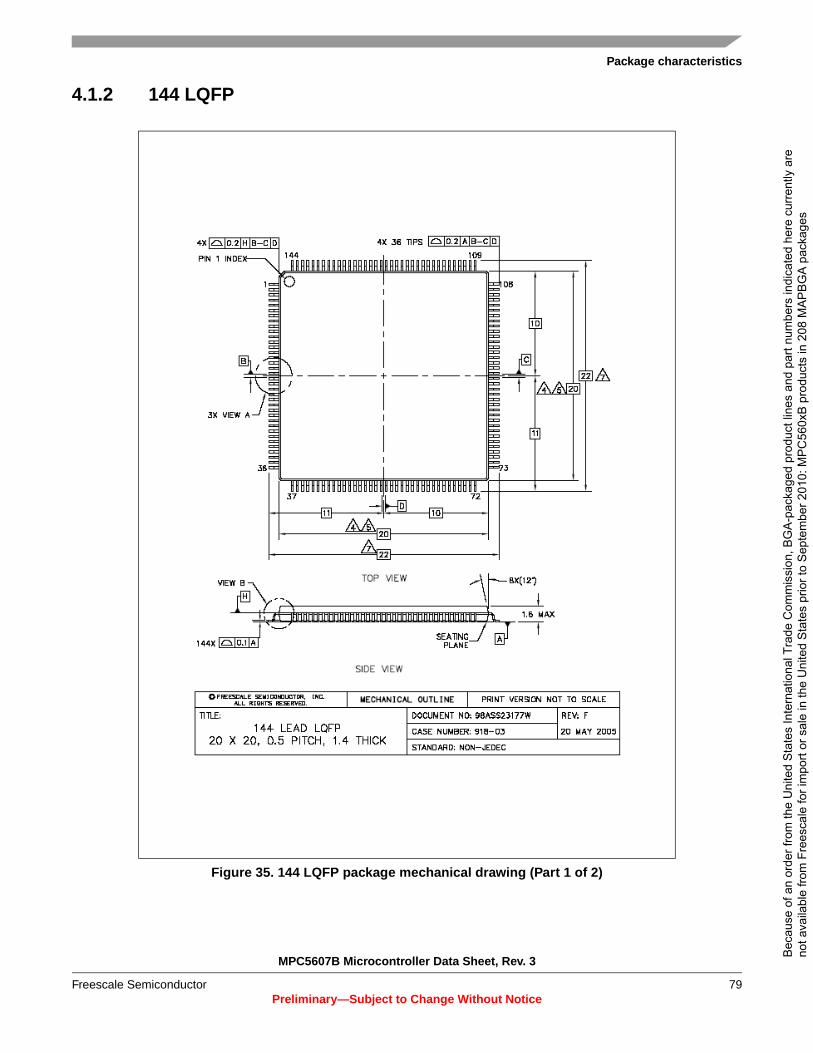
Package characteristics
MPC5607B Microcontroller Data Sheet, Rev. 3
Preliminary—Subject to Change Without NoticeFreescale Semiconductor 79
4.1.2 144 LQFP
Figure 35. 144 LQFP package mechanical drawing (Part 1 of 2)
Bec
ause
of a
n or
der f
rom
the
Uni
ted
Sta
tes
Inte
rnat
iona
l Tra
de C
omm
issi
on, B
GA
-pac
kage
d pr
oduc
t lin
es a
nd p
art n
umbe
rs in
dica
ted
here
cur
rent
ly a
re
not a
vaila
ble
from
Fre
esca
le fo
r im
port
or s
ale
in th
e U
nite
d S
tate
s pr
ior t
o S
epte
mbe
r 201
0: M
PC
560x
B p
rodu
cts
in 2
08 M
AP
BG
A p
acka
ges
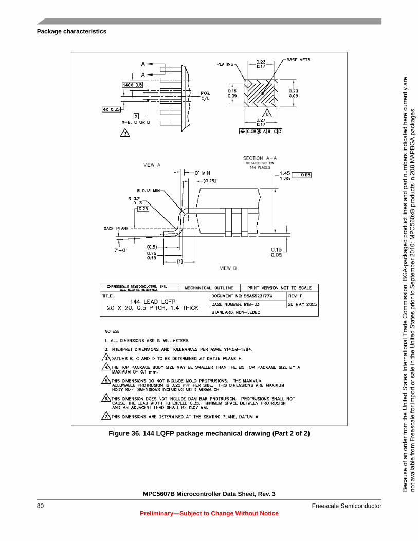
MPC5607B Microcontroller Data Sheet, Rev. 3
Preliminary—Subject to Change Without Notice
Package characteristics
Freescale Semiconductor80
Figure 36. 144 LQFP package mechanical drawing (Part 2 of 2)
Bec
ause
of a
n or
der f
rom
the
Uni
ted
Sta
tes
Inte
rnat
iona
l Tra
de C
omm
issi
on, B
GA
-pac
kage
d pr
oduc
t lin
es a
nd p
art n
umbe
rs in
dica
ted
here
cur
rent
ly a
re
not a
vaila
ble
from
Fre
esca
le fo
r im
port
or s
ale
in th
e U
nite
d S
tate
s pr
ior t
o S
epte
mbe
r 201
0: M
PC
560x
B p
rodu
cts
in 2
08 M
AP
BG
A p
acka
ges

Package characteristics
MPC5607B Microcontroller Data Sheet, Rev. 3
Preliminary—Subject to Change Without NoticeFreescale Semiconductor 81
Table 45. LQFP144 mechanical data
Symbolmm inches1
1 Values in inches are converted from mm and rounded to 4 decimal digits.
Min Typ Max Min Typ Max
A 1.600 0.0630
A1 0.050 0.150 0.0020 0.0059
A2 1.350 1.400 1.450 0.0531 0.0551 0.0571
b 0.170 0.220 0.270 0.0067 0.0087 0.0106
c 0.090 0.200 0.0035 0.0079
D 21.800 22.000 22.200 0.8583 0.8661 0.8740
D1 19.800 20.000 20.200 0.7795 0.7874 0.7953
D3 17.500 0.6890
E 21.800 22.000 22.200 0.8583 0.8661 0.8740
E1 19.800 20.000 20.200 0.7795 0.7874 0.7953
E3 17.500 0.6890
e 0.500 0.0197
L 0.450 0.600 0.750 0.0177 0.0236 0.0295
L1 1.000 0.0394
k 0.0 ° 3.5 ° 7.0° 3.5 ° 0.0 ° 7.0 °
Tolerance mm inches
ccc 0.080 0.0031
Bec
ause
of a
n or
der f
rom
the
Uni
ted
Sta
tes
Inte
rnat
iona
l Tra
de C
omm
issi
on, B
GA
-pac
kage
d pr
oduc
t lin
es a
nd p
art n
umbe
rs in
dica
ted
here
cur
rent
ly a
re
not a
vaila
ble
from
Fre
esca
le fo
r im
port
or s
ale
in th
e U
nite
d S
tate
s pr
ior t
o S
epte
mbe
r 201
0: M
PC
560x
B p
rodu
cts
in 2
08 M
AP
BG
A p
acka
ges

MPC5607B Microcontroller Data Sheet, Rev. 3
Preliminary—Subject to Change Without Notice
Package characteristics
Freescale Semiconductor82
4.1.3 100 LQFP
Figure 37. 100 LQFP package mechanical drawing (Part 1 of 3)
Bec
ause
of a
n or
der f
rom
the
Uni
ted
Sta
tes
Inte
rnat
iona
l Tra
de C
omm
issi
on, B
GA
-pac
kage
d pr
oduc
t lin
es a
nd p
art n
umbe
rs in
dica
ted
here
cur
rent
ly a
re
not a
vaila
ble
from
Fre
esca
le fo
r im
port
or s
ale
in th
e U
nite
d S
tate
s pr
ior t
o S
epte
mbe
r 201
0: M
PC
560x
B p
rodu
cts
in 2
08 M
AP
BG
A p
acka
ges

Package characteristics
MPC5607B Microcontroller Data Sheet, Rev. 3
Preliminary—Subject to Change Without NoticeFreescale Semiconductor 83
Figure 38. 100 LQFP package mechanical drawing (Part 2 of 3)
Bec
ause
of a
n or
der f
rom
the
Uni
ted
Sta
tes
Inte
rnat
iona
l Tra
de C
omm
issi
on, B
GA
-pac
kage
d pr
oduc
t lin
es a
nd p
art n
umbe
rs in
dica
ted
here
cur
rent
ly a
re
not a
vaila
ble
from
Fre
esca
le fo
r im
port
or s
ale
in th
e U
nite
d S
tate
s pr
ior t
o S
epte
mbe
r 201
0: M
PC
560x
B p
rodu
cts
in 2
08 M
AP
BG
A p
acka
ges
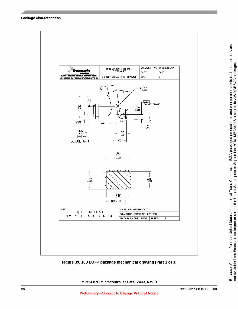
MPC5607B Microcontroller Data Sheet, Rev. 3
Preliminary—Subject to Change Without Notice
Package characteristics
Freescale Semiconductor84
Figure 39. 100 LQFP package mechanical drawing (Part 3 of 3)
Bec
ause
of a
n or
der f
rom
the
Uni
ted
Sta
tes
Inte
rnat
iona
l Tra
de C
omm
issi
on, B
GA
-pac
kage
d pr
oduc
t lin
es a
nd p
art n
umbe
rs in
dica
ted
here
cur
rent
ly a
re
not a
vaila
ble
from
Fre
esca
le fo
r im
port
or s
ale
in th
e U
nite
d S
tate
s pr
ior t
o S
epte
mbe
r 201
0: M
PC
560x
B p
rodu
cts
in 2
08 M
AP
BG
A p
acka
ges

Package characteristics
MPC5607B Microcontroller Data Sheet, Rev. 3
Preliminary—Subject to Change Without NoticeFreescale Semiconductor 85
Table 46. LQFP100 mechanical data
Symbolmm inches1
1 Values in inches are converted from mm and rounded to 4 decimal digits.
Min Typ Max Min Typ Max
A 1.600 0.0630
A1 0.050 0.150 0.0020 0.0059
A2 1.350 1.400 1.450 0.0531 0.0551 0.0571
b 0.170 0.220 0.270 0.0067 0.0087 0.0106
c 0.090 0.200 0.0035 0.0079
D 15.800 16.000 16.200 0.6220 0.6299 0.6378
D1 13.800 14.000 14.200 0.5433 0.5512 0.5591
D3 12.000 0.4724
E 15.800 16.000 16.200 0.6220 0.6299 0.6378
E1 13.800 14.000 14.200 0.5433 0.5512 0.5591
E3 12.000 0.4724
e 0.500 0.0197
L 0.450 0.600 0.750 0.0177 0.0236 0.0295
L1 1.000 0.0394
k 0.0 ° 3.5 ° 7.0 ° 0.0 ° 3.5 ° 7.0 °
Tolerance mm inches
ccc 0.080 0.0031
Bec
ause
of a
n or
der f
rom
the
Uni
ted
Sta
tes
Inte
rnat
iona
l Tra
de C
omm
issi
on, B
GA
-pac
kage
d pr
oduc
t lin
es a
nd p
art n
umbe
rs in
dica
ted
here
cur
rent
ly a
re
not a
vaila
ble
from
Fre
esca
le fo
r im
port
or s
ale
in th
e U
nite
d S
tate
s pr
ior t
o S
epte
mbe
r 201
0: M
PC
560x
B p
rodu
cts
in 2
08 M
AP
BG
A p
acka
ges

MPC5607B Microcontroller Data Sheet, Rev. 3
Preliminary—Subject to Change Without Notice
Package characteristics
Freescale Semiconductor86
4.1.4 208MAPBGA
Figure 40. 208 MAPBGA package mechanical drawing (Part 1 of 2)
Bec
ause
of a
n or
der f
rom
the
Uni
ted
Sta
tes
Inte
rnat
iona
l Tra
de C
omm
issi
on, B
GA
-pac
kage
d pr
oduc
t lin
es a
nd p
art n
umbe
rs in
dica
ted
here
cur
rent
ly a
re
not a
vaila
ble
from
Fre
esca
le fo
r im
port
or s
ale
in th
e U
nite
d S
tate
s pr
ior t
o S
epte
mbe
r 201
0: M
PC
560x
B p
rodu
cts
in 2
08 M
AP
BG
A p
acka
ges
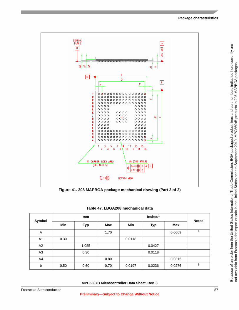
Package characteristics
MPC5607B Microcontroller Data Sheet, Rev. 3
Preliminary—Subject to Change Without NoticeFreescale Semiconductor 87
Figure 41. 208 MAPBGA package mechanical drawing (Part 2 of 2)
Table 47. LBGA208 mechanical data
Symbolmm inches1
NotesMin Typ Max Min Typ Max
A 1.70 0.0669 2
A1 0.30 0.0118
A2 1.085 0.0427
A3 0.30 0.0118
A4 0.80 0.0315
b 0.50 0.60 0.70 0.0197 0.0236 0.0276 3
Bec
ause
of a
n or
der f
rom
the
Uni
ted
Sta
tes
Inte
rnat
iona
l Tra
de C
omm
issi
on, B
GA
-pac
kage
d pr
oduc
t lin
es a
nd p
art n
umbe
rs in
dica
ted
here
cur
rent
ly a
re
not a
vaila
ble
from
Fre
esca
le fo
r im
port
or s
ale
in th
e U
nite
d S
tate
s pr
ior t
o S
epte
mbe
r 201
0: M
PC
560x
B p
rodu
cts
in 2
08 M
AP
BG
A p
acka
ges
MPC5607B Microcontroller Data Sheet, Rev. 3
Preliminary—Subject to Change Without Notice
Package characteristics
Freescale Semiconductor88
D 16.80 17.00 17.20 0.6614 0.6693 0.6772
D1 15.00 0.5906
E 16.80 17.00 17.20 0.6614 0.6693 0.6772
E1 15.00 0.5906
e 1.00 0.0394
F 1.00 0.0394
ddd 0.20 0.0079
eee 0.25 0.0098 4
fff 0.10 0.0039 5
1 Values in inches are converted from mm and rounded to 4 decimal digits.2 LBGA stands for Low profile Ball Grid Array.
- Low profile: The total profile height (Dim A) is measured from the seating plane to the top of the component- The maximum total package height is calculated by the following methodology:A2 Typ+A1 Typ +√ (A12+A32+A42 tolerance values)- Low profile: 1.20mm < A < 1.70mm
3 The typical ball diameter before mounting is 0.60mm.4 The tolerance of position that controls the location of the pattern of balls with respect to datums A and B.
For each ball there is a cylindrical tolerance zone eee perpendicular to datum C and located on true position with respect to datums A and B as defined by e. The axis perpendicular to datum C of each ball must lie within this tolerance zone.
5 The tolerance of position that controls the location of the balls within the matrix with respect to each other.For each ball there is a cylindrical tolerance zone fff perpendicular to datum C and located on true position as defined by e. The axis perpendicular to datum C of each ball must lie within this tolerance zone.Each tolerance zone fff in the array is contained entirely in the respective zone eee above.The axis of each ball must lie simultaneously in both tolerance zones.
Table 47. LBGA208 mechanical data (continued)
Symbolmm inches1
NotesMin Typ Max Min Typ Max
Bec
ause
of a
n or
der f
rom
the
Uni
ted
Sta
tes
Inte
rnat
iona
l Tra
de C
omm
issi
on, B
GA
-pac
kage
d pr
oduc
t lin
es a
nd p
art n
umbe
rs in
dica
ted
here
cur
rent
ly a
re
not a
vaila
ble
from
Fre
esca
le fo
r im
port
or s
ale
in th
e U
nite
d S
tate
s pr
ior t
o S
epte
mbe
r 201
0: M
PC
560x
B p
rodu
cts
in 2
08 M
AP
BG
A p
acka
ges

Ordering information
MPC5607B Microcontroller Data Sheet, Rev. 3
Preliminary—Subject to Change Without NoticeFreescale Semiconductor 89
5 Ordering informationFigure 42. Commercial product code structure
1 208 MAPBGA available only as development package for Nexus2+
Qualification Status
PowerPC Core
Automotive Platform
Core Version
Flash Size (core dependent)
Product
Optional fields
M PC 56 B E M LLExample code: 0 7
Temperature spec.
Package Code
Qualification Status M = MC status S = Auto qualified P = PC status
Automotive Platform 56 = PPC in 90nm 57 = PPC in 65nm
Flash Size (z0 core) 5 = 768 KB 6 = 1024 KB 7 = 1.5 MB
Product B = Body C = Gateway
R = Tape & Reel (blank if Tray)
R
Temperature spec. C = –40° C to 85°C V = –40° C to 105°C M = –40° C to 125°C
Package Code LL = 100 LQFP LQ = 144 LQFP LU= 176 LQFP
Bec
ause
of a
n or
der f
rom
the
Uni
ted
Sta
tes
Inte
rnat
iona
l Tra
de C
omm
issi
on, B
GA
-pac
kage
d pr
oduc
t lin
es a
nd p
art n
umbe
rs in
dica
ted
here
cur
rent
ly a
re
not a
vaila
ble
from
Fre
esca
le fo
r im
port
or s
ale
in th
e U
nite
d S
tate
s pr
ior t
o S
epte
mbe
r 201
0: M
PC
560x
B p
rodu
cts
in 2
08 M
AP
BG
A p
acka
ges

MPC5607B Microcontroller Data Sheet, Rev. 3
Preliminary—Subject to Change Without Notice
Revision history
Freescale Semiconductor90
6 Revision historyTable 48 summarizes revisions to this document.
Table 48. Revision history
Revision Date Substantive changes
1 12-Jan-2009 Initial release
2 09 Nov-2009 Updated Features-Replaced 27 IRQs in place of 23-ADC features-External Ballast resistor support conditions-updated device summary-added 208 BGA details-updated block diagram to include WKUP-updated block diagram to include 5 ch ADC 12 -bit-updated Block summary table-updated LQFP 144, 176 and 100 pinouts. Applied new naming convention for ADC signals as ADCx_P[x] and ADCx_S[x]Section 1, “General description-updated Bolero 1.5M device comparison table-updated block diagram-aligned with 512k-updated block summary-aligned with 512kSection 2, “Package pinouts-updated 100,144,176,208 packages according to cut2.0 changesAdded Section 3.5.1, “External ballast resistor recommendationsAdded NVUSRO [WATCHDOG_EN] field descriptionupdated Absolute maximum ratingsupdated LQFP thermal characteristicsupdated I/O supply segmentsupdated Voltage regulator capacitance connectionupdated Low voltage monitor electrical characteristicsupdated Low voltage power domain electrical characteristicsupdated DC electrical characteristicsupdated Program/Erase specificationsupdated Conversion characteristics (10 bit ADC)updated FMPLL electrical characteristicsupdated Fast RC oscillator electrical characteristics-aligned with Bolero 512Kupdated On-chip peripherals current consumptionupdated ADC characteristics and error definitions diagramupdated ADC conversion characteristics (10 bit and 12 bit)Added ADC characteristics and error definitions diagram for 12 bit ADC
3 25 Jan-2010 Updated FeaturesUpdated block diagram to connect peripherals to pad I/OUpdated block summary to include ADC 12-bitUpdated 144, 176 and 100 pinouts to adjust format issuesTable 26 Flash module life-retention value changed from 1-5 to 5 yrsMinor editing changes
Bec
ause
of a
n or
der f
rom
the
Uni
ted
Sta
tes
Inte
rnat
iona
l Tra
de C
omm
issi
on, B
GA
-pac
kage
d pr
oduc
t lin
es a
nd p
art n
umbe
rs in
dica
ted
here
cur
rent
ly a
re
not a
vaila
ble
from
Fre
esca
le fo
r im
port
or s
ale
in th
e U
nite
d S
tate
s pr
ior t
o S
epte
mbe
r 201
0: M
PC
560x
B p
rodu
cts
in 2
08 M
AP
BG
A p
acka
ges

Abbreviations
MPC5607B Microcontroller Data Sheet, Rev. 3
Preliminary—Subject to Change Without NoticeFreescale Semiconductor 91
Appendix A AbbreviationsTable 49 lists abbreviations used but not defined elsewhere in this document.
Table 49. Abbreviations
Abbreviation Meaning
CMOS Complementary metal–oxide–semiconductor
CPHA Clock phase
CPOL Clock polarity
CS Peripheral chip select
EVTO Event out
LED Light emitting diode
MCKO Message clock out
MDO Message data out
MSEO Message start/end out
MTFE Modified timing format enable
SCK Serial communications clock
SOUT Serial data out
TBD To be defined
TCK Test clock input
TDI Test data input
TDO Test data output
TMS Test mode select
Bec
ause
of a
n or
der f
rom
the
Uni
ted
Sta
tes
Inte
rnat
iona
l Tra
de C
omm
issi
on, B
GA
-pac
kage
d pr
oduc
t lin
es a
nd p
art n
umbe
rs in
dica
ted
here
cur
rent
ly a
re
not a
vaila
ble
from
Fre
esca
le fo
r im
port
or s
ale
in th
e U
nite
d S
tate
s pr
ior t
o S
epte
mbe
r 201
0: M
PC
560x
B p
rodu
cts
in 2
08 M
AP
BG
A p
acka
ges
How to Reach Us:
Home Page:www.freescale.com
Web Support:http://www.freescale.com/support
USA/Europe or Locations Not Listed:Freescale Semiconductor, Inc.Technical Information Center, EL5162100 East Elliot RoadTempe, Arizona 852841-800-521-6274 or +1-480-768-2130www.freescale.com/support
Europe, Middle East, and Africa:Freescale Halbleiter Deutschland GmbHTechnical Information CenterSchatzbogen 781829 Muenchen, Germany+44 1296 380 456 (English)+46 8 52200080 (English)+49 89 92103 559 (German)+33 1 69 35 48 48 (French)www.freescale.com/support
Japan:Freescale Semiconductor Japan Ltd. HeadquartersARCO Tower 15F1-8-1, Shimo-Meguro, Meguro-ku,Tokyo 153-0064Japan0120 191014 or +81 3 5437 [email protected]
Asia/Pacific:Freescale Semiconductor China Ltd.Exchange Building 23FNo. 118 Jianguo RoadChaoyang DistrictBeijing 100022China +86 10 5879 8000 [email protected]
Freescale Semiconductor Literature Distribution Center1-800-441-2447 or +1-303-675-2140Fax: +1-303-675-2150 [email protected]
Information in this document is provided solely to enable system and software implementers to use Freescale Semiconductor products. There are no express or implied copyright licenses granted hereunder to design or fabricate any integrated circuits or integrated circuits based on the information in this document.
Freescale Semiconductor reserves the right to make changes without further notice to any products herein. Freescale Semiconductor makes no warranty, representation or guarantee regarding the suitability of its products for any particular purpose, nor does Freescale Semiconductor assume any liability arising out of the application or use of any product or circuit, and specifically disclaims any and all liability, including without limitation consequential or incidental damages. “Typical” parameters that may be provided in Freescale Semiconductor data sheets and/or specifications can and do vary in different applications and actual performance may vary over time. All operating parameters, including “Typicals”, must be validated for each customer application by customer’s technical experts. Freescale Semiconductor does not convey any license under its patent rights nor the rights of others. Freescale Semiconductor products are not designed, intended, or authorized for use as components in systems intended for surgical implant into the body, or other applications intended to support or sustain life, or for any other application in which the failure of the Freescale Semiconductor product could create a situation where personal injury or death may occur. Should Buyer purchase or use Freescale Semiconductor products for any such unintended or unauthorized application, Buyer shall indemnify and hold Freescale Semiconductor and its officers, employees, subsidiaries, affiliates, and distributors harmless against all claims, costs, damages, and expenses, and reasonable attorney fees arising out of, directly or indirectly, any claim of personal injury or death associated with such unintended or unauthorized use, even if such claim alleges that Freescale Semiconductor was negligent regarding the design or manufacture of the part.
Freescale™ and the Freescale logo are trademarks of Freescale Semiconductor, Inc. The described product contains a PowerPC processor core. The PowerPC name is a trademark of IBM Corp. and used under license. All other product or service names are the property of their respective owners.
© Freescale Semiconductor, Inc. 2009. All rights reserved.
MPC5607BRev. 301/2010
Bec
ause
of a
n or
der f
rom
the
Uni
ted
Sta
tes
Inte
rnat
iona
l Tra
de C
omm
issi
on, B
GA
-pac
kage
d pr
oduc
t lin
es a
nd p
art n
umbe
rs in
dica
ted
here
cur
rent
ly a
re
not a
vaila
ble
from
Fre
esca
le fo
r im
port
or s
ale
in th
e U
nite
d S
tate
s pr
ior t
o S
epte
mbe
r 201
0: M
PC
560x
B p
rodu
cts
in 2
08 M
AP
BG
A p
acka
ges