mosfet - wikipedia, the free encyclopedia
TRANSCRIPT
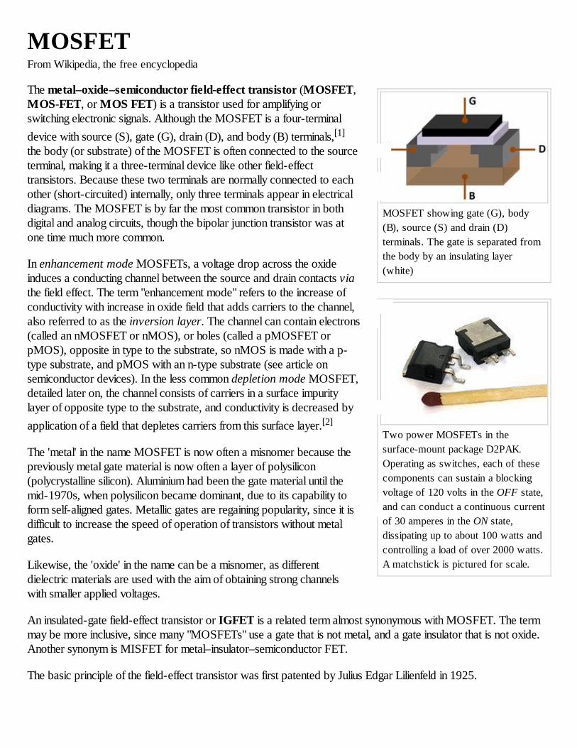
MOSFET showing gate (G), body(B), source (S) and drain (D)terminals. The gate is separated fromthe body by an insulating layer(white)
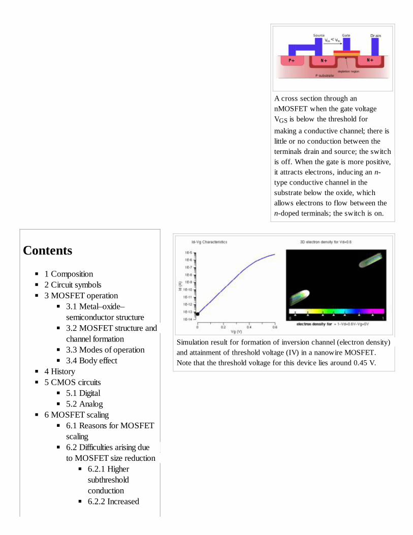
Two power MOSFETs in thesurface-mount package D2PAK.Operating as switches, each of thesecomponents can sustain a blockingvoltage of 120 volts in the OFF state,and can conduct a continuous currentof 30 amperes in the ON state,dissipating up to about 100 watts andcontrolling a load of over 2000 watts.A matchstick is pictured for scale.
MOSFETFrom Wikipedia, the free encyclopedia
The metal–oxide–semiconductor field-effect transistor (MOSFET,MOS-FET, or MOS FET) is a transistor used for amplifying orswitching electronic signals. Although the MOSFET is a four-terminaldevice with source (S), gate (G), drain (D), and body (B) terminals,[1]
the body (or substrate) of the MOSFET is often connected to the sourceterminal, making it a three-terminal device like other field-effecttransistors. Because these two terminals are normally connected to eachother (short-circuited) internally, only three terminals appear in electricaldiagrams. The MOSFET is by far the most common transistor in bothdigital and analog circuits, though the bipolar junction transistor was atone time much more common.
In enhancement mode MOSFETs, a voltage drop across the oxideinduces a conducting channel between the source and drain contacts viathe field effect. The term "enhancement mode" refers to the increase ofconductivity with increase in oxide field that adds carriers to the channel,also referred to as the inversion layer. The channel can contain electrons(called an nMOSFET or nMOS), or holes (called a pMOSFET orpMOS), opposite in type to the substrate, so nMOS is made with a p-type substrate, and pMOS with an n-type substrate (see article onsemiconductor devices). In the less common depletion mode MOSFET,detailed later on, the channel consists of carriers in a surface impuritylayer of opposite type to the substrate, and conductivity is decreased byapplication of a field that depletes carriers from this surface layer.[2]
The 'metal' in the name MOSFET is now often a misnomer because thepreviously metal gate material is now often a layer of polysilicon(polycrystalline silicon). Aluminium had been the gate material until themid-1970s, when polysilicon became dominant, due to its capability toform self-aligned gates. Metallic gates are regaining popularity, since it isdifficult to increase the speed of operation of transistors without metalgates.
Likewise, the 'oxide' in the name can be a misnomer, as differentdielectric materials are used with the aim of obtaining strong channelswith smaller applied voltages.
An insulated-gate field-effect transistor or IGFET is a related term almost synonymous with MOSFET. The termmay be more inclusive, since many "MOSFETs" use a gate that is not metal, and a gate insulator that is not oxide.Another synonym is MISFET for metal–insulator–semiconductor FET.
The basic principle of the field-effect transistor was first patented by Julius Edgar Lilienfeld in 1925.
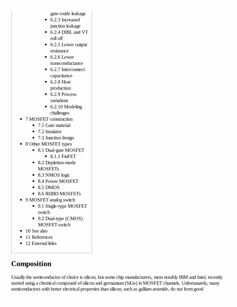
A cross section through annMOSFET when the gate voltageVGS is below the threshold formaking a conductive channel; there islittle or no conduction between theterminals drain and source; the switchis off. When the gate is more positive,it attracts electrons, inducing an n-type conductive channel in thesubstrate below the oxide, whichallows electrons to flow between then-doped terminals; the switch is on.
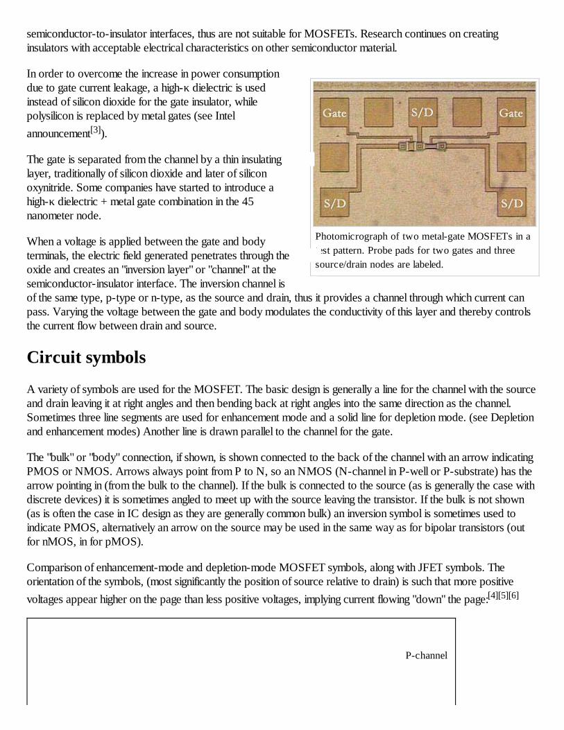
Simulation result for formation of inversion channel (electron density)and attainment of threshold voltage (IV) in a nanowire MOSFET.Note that the threshold voltage for this device lies around 0.45 V.
Contents
1 Composition2 Circuit symbols3 MOSFET operation
3.1 Metal–oxide–semiconductor structure3.2 MOSFET structure andchannel formation3.3 Modes of operation3.4 Body effect
4 History5 CMOS circuits
5.1 Digital5.2 Analog
6 MOSFET scaling6.1 Reasons for MOSFETscaling6.2 Difficulties arising dueto MOSFET size reduction
6.2.1 Highersubthresholdconduction6.2.2 Increased
gate-oxide leakage
gate-oxide leakage6.2.3 Increasedjunction leakage6.2.4 DIBL and VTroll off6.2.5 Lower outputresistance6.2.6 Lowertransconductance6.2.7 Interconnectcapacitance6.2.8 Heatproduction6.2.9 Processvariations6.2.10 Modelingchallenges
7 MOSFET construction7.1 Gate material7.2 Insulator7.3 Junction design
8 Other MOSFET types8.1 Dual-gate MOSFET
8.1.1 FinFET8.2 Depletion-modeMOSFETs8.3 NMOS logic8.4 Power MOSFET8.5 DMOS8.6 RHBD MOSFETs
9 MOSFET analog switch9.1 Single-type MOSFETswitch9.2 Dual-type (CMOS)MOSFET switch
10 See also11 References12 External links
Composition
Usually the semiconductor of choice is silicon, but some chip manufacturers, most notably IBM and Intel, recentlystarted using a chemical compound of silicon and germanium (SiGe) in MOSFET channels. Unfortunately, manysemiconductors with better electrical properties than silicon, such as gallium arsenide, do not form good
Photomicrograph of two metal-gate MOSFETs in atest pattern. Probe pads for two gates and threesource/drain nodes are labeled.
semiconductor-to-insulator interfaces, thus are not suitable for MOSFETs. Research continues on creatinginsulators with acceptable electrical characteristics on other semiconductor material.
In order to overcome the increase in power consumptiondue to gate current leakage, a high-κ dielectric is usedinstead of silicon dioxide for the gate insulator, whilepolysilicon is replaced by metal gates (see Intelannouncement[3]).
The gate is separated from the channel by a thin insulatinglayer, traditionally of silicon dioxide and later of siliconoxynitride. Some companies have started to introduce ahigh-κ dielectric + metal gate combination in the 45nanometer node.
When a voltage is applied between the gate and bodyterminals, the electric field generated penetrates through theoxide and creates an "inversion layer" or "channel" at thesemiconductor-insulator interface. The inversion channel isof the same type, p-type or n-type, as the source and drain, thus it provides a channel through which current canpass. Varying the voltage between the gate and body modulates the conductivity of this layer and thereby controlsthe current flow between drain and source.
Circuit symbols
A variety of symbols are used for the MOSFET. The basic design is generally a line for the channel with the sourceand drain leaving it at right angles and then bending back at right angles into the same direction as the channel.Sometimes three line segments are used for enhancement mode and a solid line for depletion mode. (see Depletionand enhancement modes) Another line is drawn parallel to the channel for the gate.
The "bulk" or "body" connection, if shown, is shown connected to the back of the channel with an arrow indicatingPMOS or NMOS. Arrows always point from P to N, so an NMOS (N-channel in P-well or P-substrate) has thearrow pointing in (from the bulk to the channel). If the bulk is connected to the source (as is generally the case withdiscrete devices) it is sometimes angled to meet up with the source leaving the transistor. If the bulk is not shown(as is often the case in IC design as they are generally common bulk) an inversion symbol is sometimes used toindicate PMOS, alternatively an arrow on the source may be used in the same way as for bipolar transistors (outfor nMOS, in for pMOS).
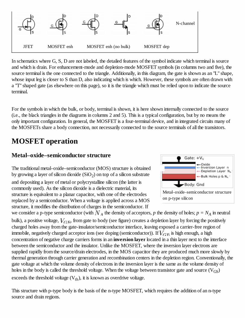
Comparison of enhancement-mode and depletion-mode MOSFET symbols, along with JFET symbols. Theorientation of the symbols, (most significantly the position of source relative to drain) is such that more positivevoltages appear higher on the page than less positive voltages, implying current flowing "down" the page:[4][5][6]
P-channel
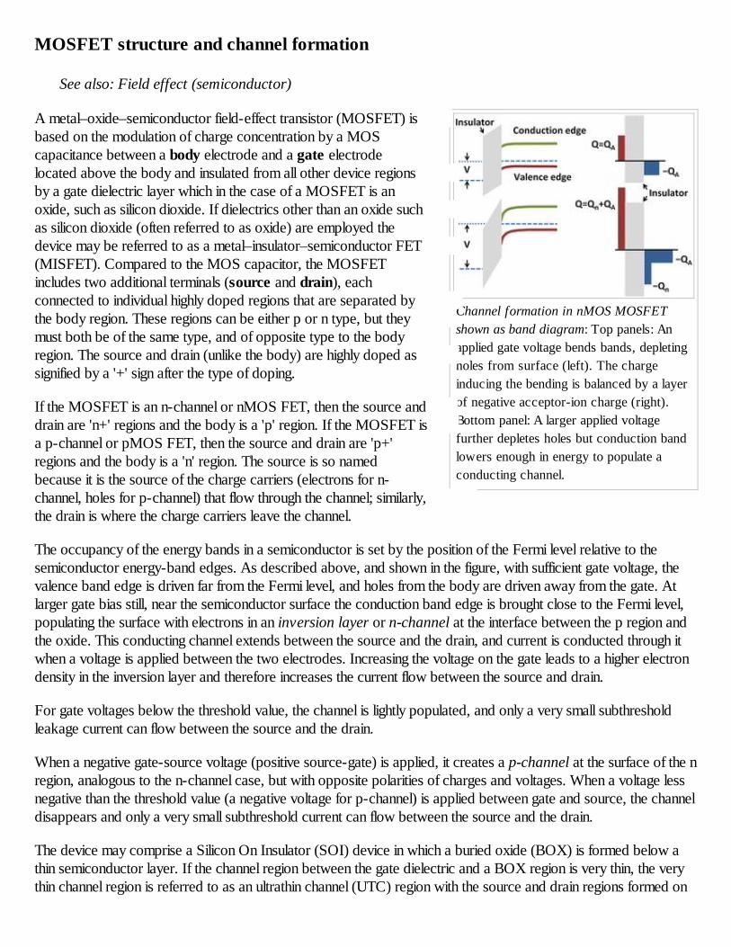
Metal–oxide–semiconductor structureon p-type silicon
N-channel
JFET MOSFET enh MOSFET enh (no bulk) MOSFET dep
In schematics where G, S, D are not labeled, the detailed features of the symbol indicate which terminal is sourceand which is drain. For enhancement-mode and depletion-mode MOSFET symbols (in columns two and five), thesource terminal is the one connected to the triangle. Additionally, in this diagram, the gate is shown as an "L" shape,whose input leg is closer to S than D, also indicating which is which. However, these symbols are often drawn witha "T" shaped gate (as elsewhere on this page), so it is the triangle which must be relied upon to indicate the sourceterminal.
For the symbols in which the bulk, or body, terminal is shown, it is here shown internally connected to the source(i.e., the black triangles in the diagrams in columns 2 and 5). This is a typical configuration, but by no means theonly important configuration. In general, the MOSFET is a four-terminal device, and in integrated circuits many ofthe MOSFETs share a body connection, not necessarily connected to the source terminals of all the transistors.
MOSFET operation
Metal–oxide–semiconductor structure
The traditional metal–oxide–semiconductor (MOS) structure is obtainedby growing a layer of silicon dioxide (SiO2) on top of a silicon substrateand depositing a layer of metal or polycrystalline silicon (the latter iscommonly used). As the silicon dioxide is a dielectric material, itsstructure is equivalent to a planar capacitor, with one of the electrodesreplaced by a semiconductor. When a voltage is applied across a MOSstructure, it modifies the distribution of charges in the semiconductor. Ifwe consider a p-type semiconductor (with the density of acceptors, p the density of holes; p = NA in neutralbulk), a positive voltage, , from gate to body (see figure) creates a depletion layer by forcing the positivelycharged holes away from the gate-insulator/semiconductor interface, leaving exposed a carrier-free region ofimmobile, negatively charged acceptor ions (see doping (semiconductor)). If is high enough, a highconcentration of negative charge carriers forms in an inversion layer located in a thin layer next to the interfacebetween the semiconductor and the insulator. Unlike the MOSFET, where the inversion layer electrons aresupplied rapidly from the source/drain electrodes, in the MOS capacitor they are produced much more slowly bythermal generation through carrier generation and recombination centers in the depletion region. Conventionally, thegate voltage at which the volume density of electrons in the inversion layer is the same as the volume density ofholes in the body is called the threshold voltage. When the voltage between transistor gate and source (VGS)exceeds the threshold voltage (Vth), it is known as overdrive voltage.
This structure with p-type body is the basis of the n-type MOSFET, which requires the addition of an n-typesource and drain regions.
Channel formation in nMOS MOSFETshown as band diagram: Top panels: Anapplied gate voltage bends bands, depletingholes from surface (left). The chargeinducing the bending is balanced by a layerof negative acceptor-ion charge (right).Bottom panel: A larger applied voltagefurther depletes holes but conduction bandlowers enough in energy to populate aconducting channel.
MOSFET structure and channel formation
See also: Field effect (semiconductor)
A metal–oxide–semiconductor field-effect transistor (MOSFET) isbased on the modulation of charge concentration by a MOScapacitance between a body electrode and a gate electrodelocated above the body and insulated from all other device regionsby a gate dielectric layer which in the case of a MOSFET is anoxide, such as silicon dioxide. If dielectrics other than an oxide suchas silicon dioxide (often referred to as oxide) are employed thedevice may be referred to as a metal–insulator–semiconductor FET(MISFET). Compared to the MOS capacitor, the MOSFETincludes two additional terminals (source and drain), eachconnected to individual highly doped regions that are separated bythe body region. These regions can be either p or n type, but theymust both be of the same type, and of opposite type to the bodyregion. The source and drain (unlike the body) are highly doped assignified by a '+' sign after the type of doping.
If the MOSFET is an n-channel or nMOS FET, then the source anddrain are 'n+' regions and the body is a 'p' region. If the MOSFET isa p-channel or pMOS FET, then the source and drain are 'p+'regions and the body is a 'n' region. The source is so namedbecause it is the source of the charge carriers (electrons for n-channel, holes for p-channel) that flow through the channel; similarly,the drain is where the charge carriers leave the channel.
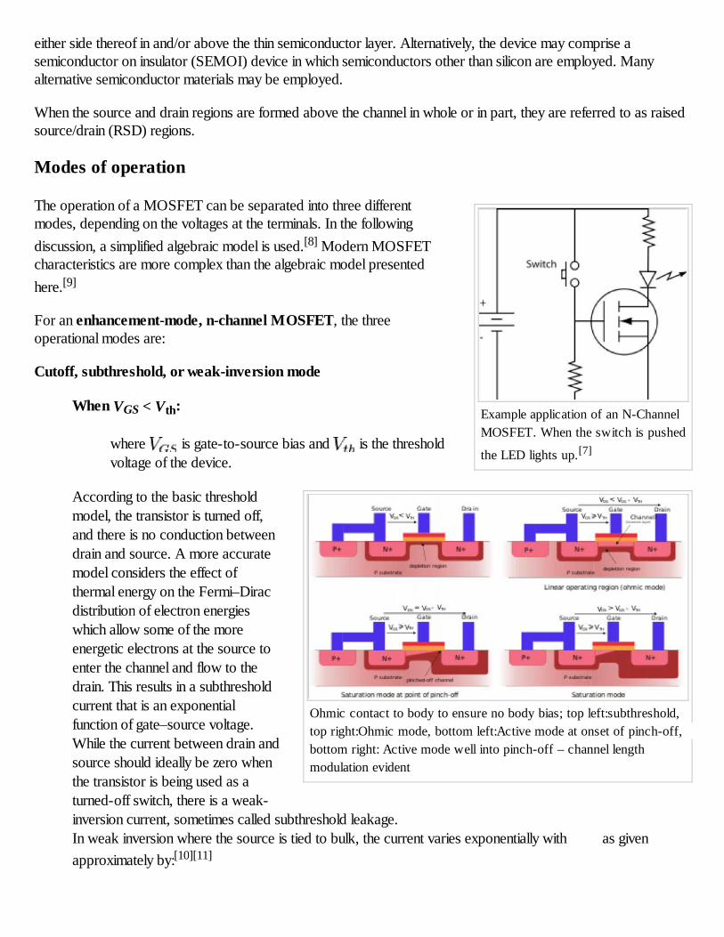
The occupancy of the energy bands in a semiconductor is set by the position of the Fermi level relative to thesemiconductor energy-band edges. As described above, and shown in the figure, with sufficient gate voltage, thevalence band edge is driven far from the Fermi level, and holes from the body are driven away from the gate. Atlarger gate bias still, near the semiconductor surface the conduction band edge is brought close to the Fermi level,populating the surface with electrons in an inversion layer or n-channel at the interface between the p region andthe oxide. This conducting channel extends between the source and the drain, and current is conducted through itwhen a voltage is applied between the two electrodes. Increasing the voltage on the gate leads to a higher electrondensity in the inversion layer and therefore increases the current flow between the source and drain.
For gate voltages below the threshold value, the channel is lightly populated, and only a very small subthresholdleakage current can flow between the source and the drain.
When a negative gate-source voltage (positive source-gate) is applied, it creates a p-channel at the surface of the nregion, analogous to the n-channel case, but with opposite polarities of charges and voltages. When a voltage lessnegative than the threshold value (a negative voltage for p-channel) is applied between gate and source, the channeldisappears and only a very small subthreshold current can flow between the source and the drain.
The device may comprise a Silicon On Insulator (SOI) device in which a buried oxide (BOX) is formed below athin semiconductor layer. If the channel region between the gate dielectric and a BOX region is very thin, the verythin channel region is referred to as an ultrathin channel (UTC) region with the source and drain regions formed on
Example application of an N-ChannelMOSFET. When the switch is pushed
the LED lights up.[7]
Ohmic contact to body to ensure no body bias; top left:subthreshold,top right:Ohmic mode, bottom left:Active mode at onset of pinch-off,bottom right: Active mode well into pinch-off – channel lengthmodulation evident
either side thereof in and/or above the thin semiconductor layer. Alternatively, the device may comprise asemiconductor on insulator (SEMOI) device in which semiconductors other than silicon are employed. Manyalternative semiconductor materials may be employed.
When the source and drain regions are formed above the channel in whole or in part, they are referred to as raisedsource/drain (RSD) regions.
Modes of operation
The operation of a MOSFET can be separated into three differentmodes, depending on the voltages at the terminals. In the followingdiscussion, a simplified algebraic model is used.[8] Modern MOSFETcharacteristics are more complex than the algebraic model presentedhere.[9]
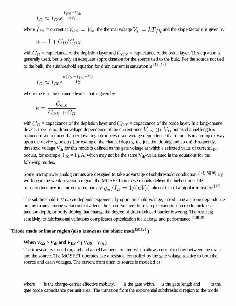
For an enhancement-mode, n-channel MOSFET, the threeoperational modes are:
Cutoff, subthreshold, or weak-inversion mode
When VGS < Vth:
where is gate-to-source bias and is the thresholdvoltage of the device.
According to the basic thresholdmodel, the transistor is turned off,and there is no conduction betweendrain and source. A more accuratemodel considers the effect ofthermal energy on the Fermi–Diracdistribution of electron energieswhich allow some of the moreenergetic electrons at the source toenter the channel and flow to thedrain. This results in a subthresholdcurrent that is an exponentialfunction of gate–source voltage.While the current between drain andsource should ideally be zero whenthe transistor is being used as aturned-off switch, there is a weak-inversion current, sometimes called subthreshold leakage.In weak inversion where the source is tied to bulk, the current varies exponentially with as givenapproximately by:[10][11]
where = current at , the thermal voltage and the slope factor n is given by
with = capacitance of the depletion layer and = capacitance of the oxide layer. This equation isgenerally used, but is only an adequate approximation for the source tied to the bulk. For the source not tiedto the bulk, the subthreshold equation for drain current in saturation is [12][13]
where the is the channel divider that is given by
with = capacitance of the depletion layer and = capacitance of the oxide layer. In a long-channeldevice, there is no drain voltage dependence of the current once , but as channel length isreduced drain-induced barrier lowering introduces drain voltage dependence that depends in a complex wayupon the device geometry (for example, the channel doping, the junction doping and so on). Frequently,threshold voltage Vth for this mode is defined as the gate voltage at which a selected value of current ID0occurs, for example, ID0 = 1 μA, which may not be the same Vth-value used in the equations for thefollowing modes.
Some micropower analog circuits are designed to take advantage of subthreshold conduction.[14][15][16] Byworking in the weak-inversion region, the MOSFETs in these circuits deliver the highest possibletransconductance-to-current ratio, namely: , almost that of a bipolar transistor.[17]
The subthreshold I–V curve depends exponentially upon threshold voltage, introducing a strong dependenceon any manufacturing variation that affects threshold voltage; for example: variations in oxide thickness,junction depth, or body doping that change the degree of drain-induced barrier lowering. The resultingsensitivity to fabricational variations complicates optimization for leakage and performance.[18][19]
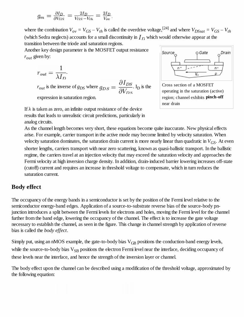
Triode mode or linear region (also known as the ohmic mode[20][21])
When VGS > Vth and VDS < ( VGS – Vth )The transistor is turned on, and a channel has been created which allows current to flow between the drainand the source. The MOSFET operates like a resistor, controlled by the gate voltage relative to both thesource and drain voltages. The current from drain to source is modeled as:
where is the charge-carrier effective mobility, is the gate width, is the gate length and is thegate oxide capacitance per unit area. The transition from the exponential subthreshold region to the triode
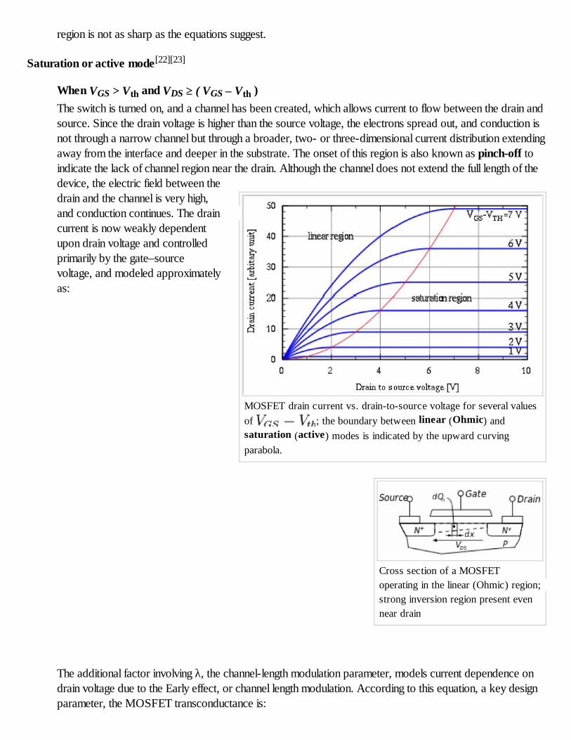
MOSFET drain current vs. drain-to-source voltage for several valuesof ; the boundary between linear (Ohmic) andsaturation (active) modes is indicated by the upward curvingparabola.
Cross section of a MOSFEToperating in the linear (Ohmic) region;strong inversion region present evennear drain
region is not as sharp as the equations suggest.
Saturation or active mode[22][23]
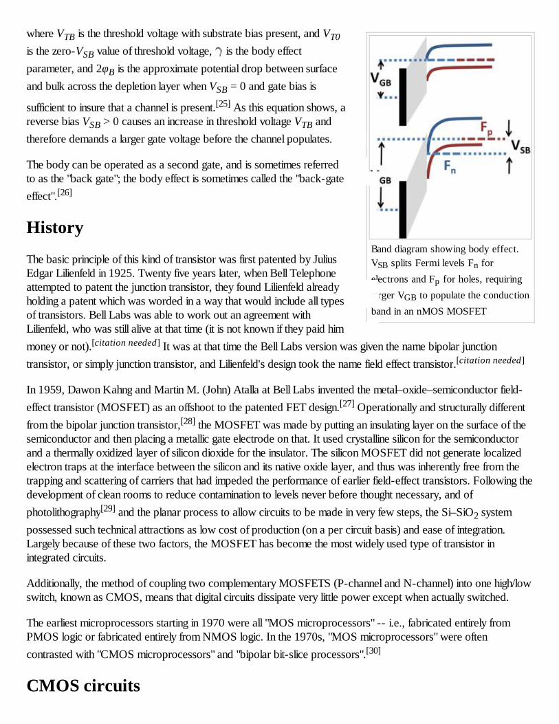
When VGS > Vth and VDS ≥ ( VGS – Vth )The switch is turned on, and a channel has been created, which allows current to flow between the drain andsource. Since the drain voltage is higher than the source voltage, the electrons spread out, and conduction isnot through a narrow channel but through a broader, two- or three-dimensional current distribution extendingaway from the interface and deeper in the substrate. The onset of this region is also known as pinch-off toindicate the lack of channel region near the drain. Although the channel does not extend the full length of thedevice, the electric field between thedrain and the channel is very high,and conduction continues. The draincurrent is now weakly dependentupon drain voltage and controlledprimarily by the gate–sourcevoltage, and modeled approximatelyas:
The additional factor involving λ, the channel-length modulation parameter, models current dependence ondrain voltage due to the Early effect, or channel length modulation. According to this equation, a key designparameter, the MOSFET transconductance is:
Cross section of a MOSFEToperating in the saturation (active)region; channel exhibits pinch-offnear drain
where the combination Vov = VGS – Vth is called the overdrive voltage,[24] and where VDSsat = VGS – Vth(which Sedra neglects) accounts for a small discontinuity in which would otherwise appear at thetransition between the triode and saturation regions.Another key design parameter is the MOSFET output resistancerout given by:
.
rout is the inverse of gDS where . ID is the
expression in saturation region.
If λ is taken as zero, an infinite output resistance of the deviceresults that leads to unrealistic circuit predictions, particularly inanalog circuits.As the channel length becomes very short, these equations become quite inaccurate. New physical effectsarise. For example, carrier transport in the active mode may become limited by velocity saturation. Whenvelocity saturation dominates, the saturation drain current is more nearly linear than quadratic in VGS. At evenshorter lengths, carriers transport with near zero scattering, known as quasi-ballistic transport. In the ballisticregime, the carriers travel at an injection velocity that may exceed the saturation velocity and approaches theFermi velocity at high inversion charge density. In addition, drain-induced barrier lowering increases off-state(cutoff) current and requires an increase in threshold voltage to compensate, which in turn reduces thesaturation current.
Body effect
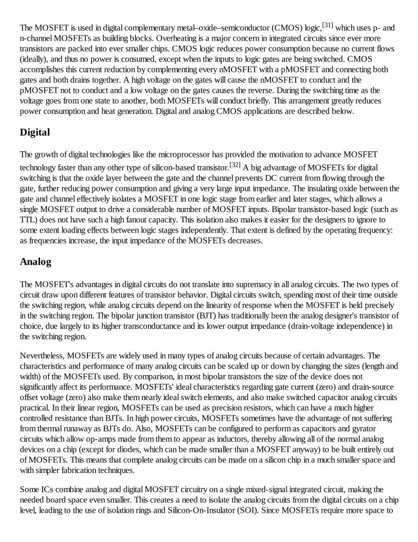
The occupancy of the energy bands in a semiconductor is set by the position of the Fermi level relative to thesemiconductor energy-band edges. Application of a source-to-substrate reverse bias of the source-body pn-junction introduces a split between the Fermi levels for electrons and holes, moving the Fermi level for the channelfurther from the band edge, lowering the occupancy of the channel. The effect is to increase the gate voltagenecessary to establish the channel, as seen in the figure. This change in channel strength by application of reversebias is called the body effect.
Simply put, using an nMOS example, the gate-to-body bias VGB positions the conduction-band energy levels,while the source-to-body bias VSB positions the electron Fermi level near the interface, deciding occupancy ofthese levels near the interface, and hence the strength of the inversion layer or channel.
The body effect upon the channel can be described using a modification of the threshold voltage, approximated bythe following equation:
Band diagram showing body effect.VSB splits Fermi levels Fn forelectrons and Fp for holes, requiringlarger VGB to populate the conductionband in an nMOS MOSFET
where VTB is the threshold voltage with substrate bias present, and VT0is the zero-VSB value of threshold voltage, is the body effectparameter, and 2φB is the approximate potential drop between surfaceand bulk across the depletion layer when VSB = 0 and gate bias is
sufficient to insure that a channel is present.[25] As this equation shows, areverse bias VSB > 0 causes an increase in threshold voltage VTB andtherefore demands a larger gate voltage before the channel populates.
The body can be operated as a second gate, and is sometimes referredto as the "back gate"; the body effect is sometimes called the "back-gateeffect".[26]
History
The basic principle of this kind of transistor was first patented by JuliusEdgar Lilienfeld in 1925. Twenty five years later, when Bell Telephoneattempted to patent the junction transistor, they found Lilienfeld alreadyholding a patent which was worded in a way that would include all typesof transistors. Bell Labs was able to work out an agreement withLilienfeld, who was still alive at that time (it is not known if they paid himmoney or not).[citation needed] It was at that time the Bell Labs version was given the name bipolar junctiontransistor, or simply junction transistor, and Lilienfeld's design took the name field effect transistor.[citation needed]
In 1959, Dawon Kahng and Martin M. (John) Atalla at Bell Labs invented the metal–oxide–semiconductor field-effect transistor (MOSFET) as an offshoot to the patented FET design.[27] Operationally and structurally differentfrom the bipolar junction transistor,[28] the MOSFET was made by putting an insulating layer on the surface of thesemiconductor and then placing a metallic gate electrode on that. It used crystalline silicon for the semiconductorand a thermally oxidized layer of silicon dioxide for the insulator. The silicon MOSFET did not generate localizedelectron traps at the interface between the silicon and its native oxide layer, and thus was inherently free from thetrapping and scattering of carriers that had impeded the performance of earlier field-effect transistors. Following thedevelopment of clean rooms to reduce contamination to levels never before thought necessary, and ofphotolithography[29] and the planar process to allow circuits to be made in very few steps, the Si–SiO2 systempossessed such technical attractions as low cost of production (on a per circuit basis) and ease of integration.Largely because of these two factors, the MOSFET has become the most widely used type of transistor inintegrated circuits.
Additionally, the method of coupling two complementary MOSFETS (P-channel and N-channel) into one high/lowswitch, known as CMOS, means that digital circuits dissipate very little power except when actually switched.
The earliest microprocessors starting in 1970 were all "MOS microprocessors" -- i.e., fabricated entirely fromPMOS logic or fabricated entirely from NMOS logic. In the 1970s, "MOS microprocessors" were oftencontrasted with "CMOS microprocessors" and "bipolar bit-slice processors".[30]
CMOS circuits
The MOSFET is used in digital complementary metal–oxide–semiconductor (CMOS) logic,[31] which uses p- andn-channel MOSFETs as building blocks. Overheating is a major concern in integrated circuits since ever moretransistors are packed into ever smaller chips. CMOS logic reduces power consumption because no current flows(ideally), and thus no power is consumed, except when the inputs to logic gates are being switched. CMOSaccomplishes this current reduction by complementing every nMOSFET with a pMOSFET and connecting bothgates and both drains together. A high voltage on the gates will cause the nMOSFET to conduct and thepMOSFET not to conduct and a low voltage on the gates causes the reverse. During the switching time as thevoltage goes from one state to another, both MOSFETs will conduct briefly. This arrangement greatly reducespower consumption and heat generation. Digital and analog CMOS applications are described below.
Digital
The growth of digital technologies like the microprocessor has provided the motivation to advance MOSFETtechnology faster than any other type of silicon-based transistor.[32] A big advantage of MOSFETs for digitalswitching is that the oxide layer between the gate and the channel prevents DC current from flowing through thegate, further reducing power consumption and giving a very large input impedance. The insulating oxide between thegate and channel effectively isolates a MOSFET in one logic stage from earlier and later stages, which allows asingle MOSFET output to drive a considerable number of MOSFET inputs. Bipolar transistor-based logic (such asTTL) does not have such a high fanout capacity. This isolation also makes it easier for the designers to ignore tosome extent loading effects between logic stages independently. That extent is defined by the operating frequency:as frequencies increase, the input impedance of the MOSFETs decreases.
Analog
The MOSFET's advantages in digital circuits do not translate into supremacy in all analog circuits. The two types ofcircuit draw upon different features of transistor behavior. Digital circuits switch, spending most of their time outsidethe switching region, while analog circuits depend on the linearity of response when the MOSFET is held preciselyin the switching region. The bipolar junction transistor (BJT) has traditionally been the analog designer's transistor ofchoice, due largely to its higher transconductance and its lower output impedance (drain-voltage independence) inthe switching region.
Nevertheless, MOSFETs are widely used in many types of analog circuits because of certain advantages. Thecharacteristics and performance of many analog circuits can be scaled up or down by changing the sizes (length andwidth) of the MOSFETs used. By comparison, in most bipolar transistors the size of the device does notsignificantly affect its performance. MOSFETs' ideal characteristics regarding gate current (zero) and drain-sourceoffset voltage (zero) also make them nearly ideal switch elements, and also make switched capacitor analog circuitspractical. In their linear region, MOSFETs can be used as precision resistors, which can have a much highercontrolled resistance than BJTs. In high power circuits, MOSFETs sometimes have the advantage of not sufferingfrom thermal runaway as BJTs do. Also, MOSFETs can be configured to perform as capacitors and gyratorcircuits which allow op-amps made from them to appear as inductors, thereby allowing all of the normal analogdevices on a chip (except for diodes, which can be made smaller than a MOSFET anyway) to be built entirely outof MOSFETs. This means that complete analog circuits can be made on a silicon chip in a much smaller space andwith simpler fabrication techniques.
Some ICs combine analog and digital MOSFET circuitry on a single mixed-signal integrated circuit, making theneeded board space even smaller. This creates a need to isolate the analog circuits from the digital circuits on a chiplevel, leading to the use of isolation rings and Silicon-On-Insulator (SOI). Since MOSFETs require more space to
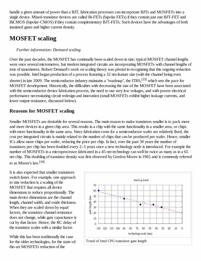
Trend of Intel CPU transistor gate length
handle a given amount of power than a BJT, fabrication processes can incorporate BJTs and MOSFETs into asingle device. Mixed-transistor devices are called Bi-FETs (bipolar FETs) if they contain just one BJT-FET andBiCMOS (bipolar-CMOS) if they contain complementary BJT-FETs. Such devices have the advantages of bothinsulated gates and higher current density.
MOSFET scaling
Further information: Dennard scaling
Over the past decades, the MOSFET has continually been scaled down in size; typical MOSFET channel lengthswere once several micrometres, but modern integrated circuits are incorporating MOSFETs with channel lengths oftens of nanometers. Robert Dennard's work on scaling theory was pivotal in recognising that this ongoing reductionwas possible. Intel began production of a process featuring a 32 nm feature size (with the channel being evenshorter) in late 2009. The semiconductor industry maintains a "roadmap", the ITRS,[33] which sets the pace forMOSFET development. Historically, the difficulties with decreasing the size of the MOSFET have been associatedwith the semiconductor device fabrication process, the need to use very low voltages, and with poorer electricalperformance necessitating circuit redesign and innovation (small MOSFETs exhibit higher leakage currents, andlower output resistance, discussed below).
Reasons for MOSFET scaling
Smaller MOSFETs are desirable for several reasons. The main reason to make transistors smaller is to pack moreand more devices in a given chip area. This results in a chip with the same functionality in a smaller area, or chipswith more functionality in the same area. Since fabrication costs for a semiconductor wafer are relatively fixed, thecost per integrated circuits is mainly related to the number of chips that can be produced per wafer. Hence, smallerICs allow more chips per wafer, reducing the price per chip. In fact, over the past 30 years the number oftransistors per chip has been doubled every 2–3 years once a new technology node is introduced. For example thenumber of MOSFETs in a microprocessor fabricated in a 45 nm technology can well be twice as many as in a 65nm chip. This doubling of transistor density was first observed by Gordon Moore in 1965 and is commonly referredto as Moore's law.[34]
It is also expected that smaller transistorsswitch faster. For example, one approachto size reduction is a scaling of theMOSFET that requires all devicedimensions to reduce proportionally. Themain device dimensions are the channellength, channel width, and oxide thickness.When they are scaled down by equalfactors, the transistor channel resistancedoes not change, while gate capacitance iscut by that factor. Hence, the RC delay ofthe transistor scales with a similar factor.
While this has been traditionally the casefor the older technologies, for the state-of-the-art MOSFETs reduction of the

transistor dimensions does not necessarily translate to higher chip speed because the delay due to interconnectionsis more significant.
Difficulties arising due to MOSFET size reduction
Producing MOSFETs with channel lengths much smaller than a micrometre is a challenge, and the difficulties ofsemiconductor device fabrication are always a limiting factor in advancing integrated circuit technology. In recentyears, the small size of the MOSFET, below a few tens of nanometers, has created operational problems.
Higher subthreshold conduction
As MOSFET geometries shrink, the voltage that can be applied to the gate must be reduced to maintain reliability.To maintain performance, the threshold voltage of the MOSFET has to be reduced as well. As threshold voltage isreduced, the transistor cannot be switched from complete turn-off to complete turn-on with the limited voltageswing available; the circuit design is a compromise between strong current in the "on" case and low current in the"off" case, and the application determines whether to favor one over the other. Subthreshold leakage (includingsubthreshold conduction, gate-oxide leakage and reverse-biased junction leakage), which was ignored in the past,now can consume upwards of half of the total power consumption of modern high-performance VLSIchips.[35][36][37]
Increased gate-oxide leakage
The gate oxide, which serves as insulator between the gate and channel, should be made as thin as possible toincrease the channel conductivity and performance when the transistor is on and to reduce subthreshold leakagewhen the transistor is off. However, with current gate oxides with a thickness of around 1.2 nm (which in silicon is~5 atoms thick) the quantum mechanical phenomenon of electron tunneling occurs between the gate and channel,leading to increased power consumption.
Silicon dioxide has traditionally been used as the gate insulator. Silicon dioxide however has a modest dielectricconstant. Increasing the dielectric constant of the gate dielectric allows a thicker layer while maintaining a highcapacitance (capacitance is proportional to dielectric constant and inversely proportional to dielectric thickness). Allelse equal, a higher dielectric thickness reduces the quantum tunneling current through the dielectric between thegate and the channel.
Insulators that have a larger dielectric constant than silicon dioxide (referred to as high-k dielectrics), such as groupIVb metal silicates e.g. hafnium and zirconium silicates and oxides are being used to reduce the gate leakage fromthe 45 nanometer technology node onwards.
On the other hand, the barrier height of the new gate insulator is an important consideration; the difference inconduction band energy between the semiconductor and the dielectric (and the corresponding difference in valenceband energy) also affects leakage current level. For the traditional gate oxide, silicon dioxide, the former barrier isapproximately 8 eV. For many alternative dielectrics the value is significantly lower, tending to increase the tunnelingcurrent, somewhat negating the advantage of higher dielectric constant.
The maximum gate-source voltage is determined by the strength of the electric field able to be sustained by the gatedielectric before significant leakage occurs. As the insulating dielectric is made thinner, the electric field strengthwithin it goes up for a fixed voltage. This necessitates using lower voltages with the thinner dielectric.
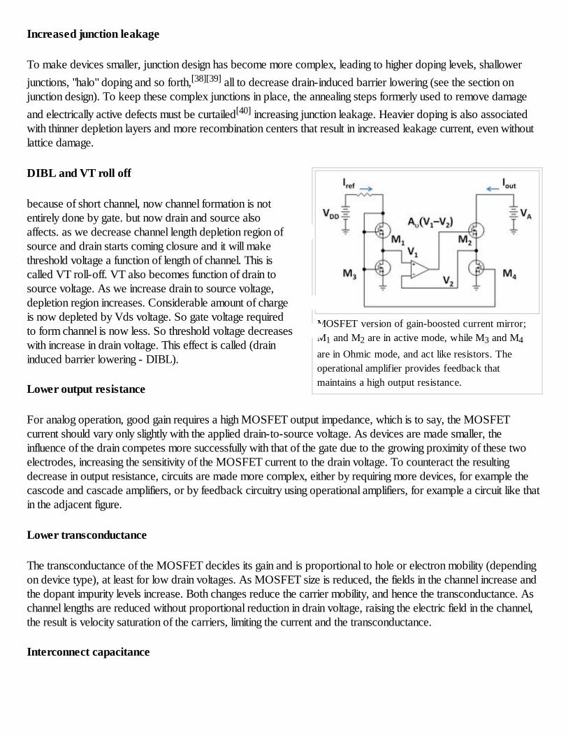
MOSFET version of gain-boosted current mirror;M1 and M2 are in active mode, while M3 and M4are in Ohmic mode, and act like resistors. Theoperational amplifier provides feedback thatmaintains a high output resistance.
Increased junction leakage
To make devices smaller, junction design has become more complex, leading to higher doping levels, shallowerjunctions, "halo" doping and so forth,[38][39] all to decrease drain-induced barrier lowering (see the section onjunction design). To keep these complex junctions in place, the annealing steps formerly used to remove damageand electrically active defects must be curtailed[40] increasing junction leakage. Heavier doping is also associatedwith thinner depletion layers and more recombination centers that result in increased leakage current, even withoutlattice damage.
DIBL and VT roll off
because of short channel, now channel formation is notentirely done by gate. but now drain and source alsoaffects. as we decrease channel length depletion region ofsource and drain starts coming closure and it will makethreshold voltage a function of length of channel. This iscalled VT roll-off. VT also becomes function of drain tosource voltage. As we increase drain to source voltage,depletion region increases. Considerable amount of chargeis now depleted by Vds voltage. So gate voltage requiredto form channel is now less. So threshold voltage decreaseswith increase in drain voltage. This effect is called (draininduced barrier lowering - DIBL).
Lower output resistance
For analog operation, good gain requires a high MOSFET output impedance, which is to say, the MOSFETcurrent should vary only slightly with the applied drain-to-source voltage. As devices are made smaller, theinfluence of the drain competes more successfully with that of the gate due to the growing proximity of these twoelectrodes, increasing the sensitivity of the MOSFET current to the drain voltage. To counteract the resultingdecrease in output resistance, circuits are made more complex, either by requiring more devices, for example thecascode and cascade amplifiers, or by feedback circuitry using operational amplifiers, for example a circuit like thatin the adjacent figure.
Lower transconductance
The transconductance of the MOSFET decides its gain and is proportional to hole or electron mobility (dependingon device type), at least for low drain voltages. As MOSFET size is reduced, the fields in the channel increase andthe dopant impurity levels increase. Both changes reduce the carrier mobility, and hence the transconductance. Aschannel lengths are reduced without proportional reduction in drain voltage, raising the electric field in the channel,the result is velocity saturation of the carriers, limiting the current and the transconductance.
Interconnect capacitance
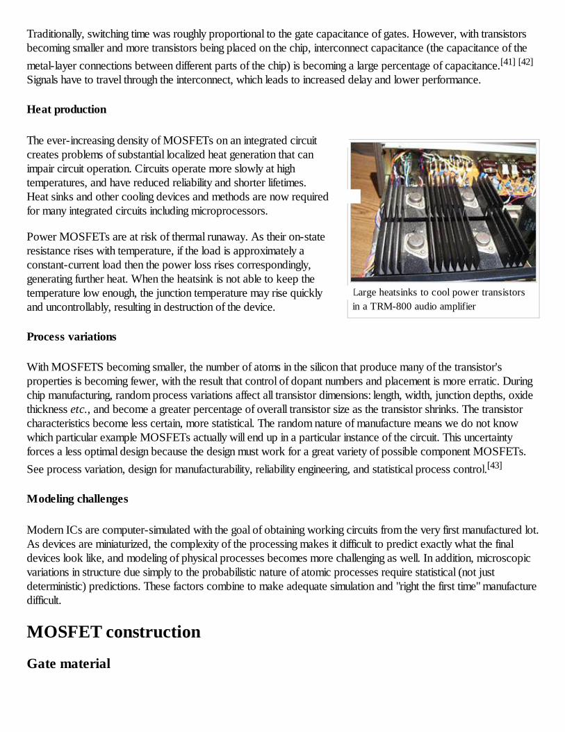
Large heatsinks to cool power transistorsin a TRM-800 audio amplifier
Traditionally, switching time was roughly proportional to the gate capacitance of gates. However, with transistorsbecoming smaller and more transistors being placed on the chip, interconnect capacitance (the capacitance of themetal-layer connections between different parts of the chip) is becoming a large percentage of capacitance.[41] [42]
Signals have to travel through the interconnect, which leads to increased delay and lower performance.
Heat production
The ever-increasing density of MOSFETs on an integrated circuitcreates problems of substantial localized heat generation that canimpair circuit operation. Circuits operate more slowly at hightemperatures, and have reduced reliability and shorter lifetimes.Heat sinks and other cooling devices and methods are now requiredfor many integrated circuits including microprocessors.
Power MOSFETs are at risk of thermal runaway. As their on-stateresistance rises with temperature, if the load is approximately aconstant-current load then the power loss rises correspondingly,generating further heat. When the heatsink is not able to keep thetemperature low enough, the junction temperature may rise quicklyand uncontrollably, resulting in destruction of the device.
Process variations
With MOSFETS becoming smaller, the number of atoms in the silicon that produce many of the transistor'sproperties is becoming fewer, with the result that control of dopant numbers and placement is more erratic. Duringchip manufacturing, random process variations affect all transistor dimensions: length, width, junction depths, oxidethickness etc., and become a greater percentage of overall transistor size as the transistor shrinks. The transistorcharacteristics become less certain, more statistical. The random nature of manufacture means we do not knowwhich particular example MOSFETs actually will end up in a particular instance of the circuit. This uncertaintyforces a less optimal design because the design must work for a great variety of possible component MOSFETs.See process variation, design for manufacturability, reliability engineering, and statistical process control.[43]
Modeling challenges
Modern ICs are computer-simulated with the goal of obtaining working circuits from the very first manufactured lot.As devices are miniaturized, the complexity of the processing makes it difficult to predict exactly what the finaldevices look like, and modeling of physical processes becomes more challenging as well. In addition, microscopicvariations in structure due simply to the probabilistic nature of atomic processes require statistical (not justdeterministic) predictions. These factors combine to make adequate simulation and "right the first time" manufacturedifficult.
MOSFET construction
Gate material
The primary criterion for the gate material is that it is a good conductor. Highly doped polycrystalline silicon is anacceptable but certainly not ideal conductor, and also suffers from some more technical deficiencies in its role as thestandard gate material. Nevertheless, there are several reasons favoring use of polysilicon:
1. The threshold voltage (and consequently the drain to source on-current) is modified by the work functiondifference between the gate material and channel material. Because polysilicon is a semiconductor, its workfunction can be modulated by adjusting the type and level of doping. Furthermore, because polysilicon hasthe same bandgap as the underlying silicon channel, it is quite straightforward to tune the work function toachieve low threshold voltages for both NMOS and PMOS devices. By contrast, the work functions ofmetals are not easily modulated, so tuning the work function to obtain low threshold voltages becomes asignificant challenge. Additionally, obtaining low-threshold devices on both PMOS and NMOS deviceswould likely require the use of different metals for each device type, introducing additional complexity to thefabrication process.
2. The silicon-SiO2 interface has been well studied and is known to have relatively few defects. By contrastmany metal–insulator interfaces contain significant levels of defects which can lead to Fermi level pinning,charging, or other phenomena that ultimately degrade device performance.
3. In the MOSFET IC fabrication process, it is preferable to deposit the gate material prior to certain high-temperature steps in order to make better-performing transistors. Such high temperature steps would meltsome metals, limiting the types of metal that can be used in a metal-gate-based process.
While polysilicon gates have been the de facto standard for the last twenty years, they do have some disadvantageswhich have led to their likely future replacement by metal gates. These disadvantages include:
Polysilicon is not a great conductor (approximately 1000 times more resistive than metals) which reduces thesignal propagation speed through the material. The resistivity can be lowered by increasing the level ofdoping, but even highly doped polysilicon is not as conductive as most metals. To improve conductivityfurther, sometimes a high-temperature metal such as tungsten, titanium, cobalt, and more recently nickel isalloyed with the top layers of the polysilicon. Such a blended material is called silicide. The silicide-polysilicon combination has better electrical properties than polysilicon alone and still does not melt insubsequent processing. Also the threshold voltage is not significantly higher than with polysilicon alone,because the silicide material is not near the channel. The process in which silicide is formed on both the gateelectrode and the source and drain regions is sometimes called salicide, self-aligned silicide.When the transistors are extremely scaled down, it is necessary to make the gate dielectric layer very thin,around 1 nm in state-of-the-art technologies. A phenomenon observed here is the so-called poly depletion,where a depletion layer is formed in the gate polysilicon layer next to the gate dielectric when the transistor isin the inversion. To avoid this problem, a metal gate is desired. A variety of metal gates such as tantalum,tungsten, tantalum nitride, and titanium nitride are used, usually in conjunction with high-k dielectrics. Analternative is to use fully silicided polysilicon gates, a process known as FUSI.
Present high performance CPUs use metal gate technology, together with high-k dielectrics, a combination knownas HKMG (High-K, Metal Gate). The disadvantages of metal gates are overcome by a few techniques:[44]
1. The threshold voltage is tuned by including a thin "work function metal" layer between the high-K dielectricand the main metal. This layer is thin enough that the total work function of the gate is influenced by both themain metal and thin metal work functions (either due to alloying during annealing, or simply due to theincomplete screening by the thin metal). The threshold voltage thus can be tuned by the thickness of the thin
metal layer.2. High-K dielectrics are now well studied, and their defects are understood.3. HKMG processes exist that do not require the metals to experience high temperature anneals; other
processes select metals that can survive the annealing step.
Insulator
As devices are made smaller, insulating layers are made thinner, and at some point tunneling of carriers through theinsulator from the channel to the gate electrode takes place. To reduce the resulting leakage current, the insulatorcan be made thicker by choosing a material with a higher dielectric constant. To see how thickness and dielectricconstant are related, note that Gauss' law connects field to charge as:
with Q = charge density, κ = dielectric constant, ε0 = permittivity of empty space and E = electric field. From thislaw it appears the same charge can be maintained in the channel at a lower field provided κ is increased. Thevoltage on the gate is given by:
with VG = gate voltage, Vch = voltage at channel side of insulator, and tins = insulator thickness. This equationshows the gate voltage will not increase when the insulator thickness increases, provided κ increases to keep tins /κ= constant (see the article on high-κ dielectrics for more detail, and the section in this article on gate-oxideleakage).
The insulator in a MOSFET is a dielectric which can in any event be silicon oxide, but many other dielectricmaterials are employed. The generic term for the dielectric is gate dielectric since the dielectric lies directly belowthe gate electrode and above the channel of the MOSFET.
Junction design
The source-to-body and drain-to-body junctions are the object of much attention because of three major factors:their design affects the current-voltage (I-V) characteristics of the device, lowering output resistance, and also thespeed of the device through the loading effect of the junction capacitances, and finally, the component of stand-bypower dissipation due to junction leakage.
The drain induced barrier lowering of the threshold voltage and channel length modulation effects upon I-V curvesare reduced by using shallow junction extensions. In addition, halo doping can be used, that is, the addition of verythin heavily doped regions of the same doping type as the body tight against the junction walls to limit the extent ofdepletion regions.[45]
The capacitive effects are limited by using raised source and drain geometries that make most of the contact areaborder thick dielectric instead of silicon. [46]
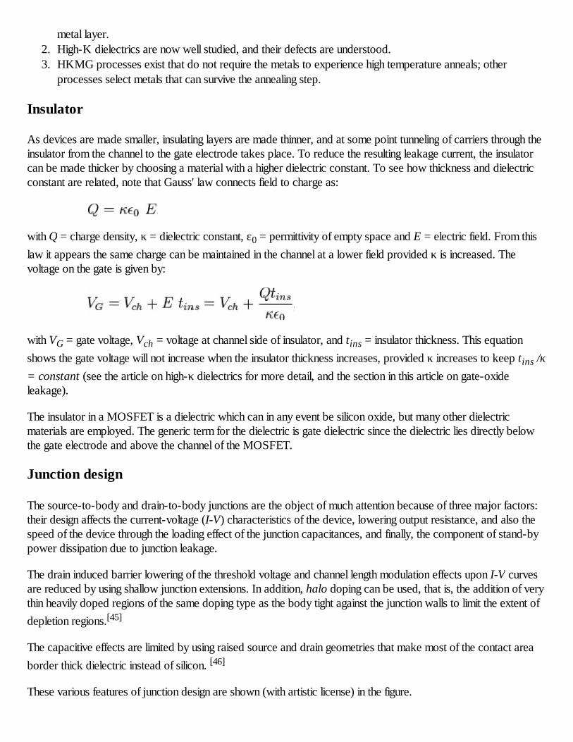
These various features of junction design are shown (with artistic license) in the figure.
MOSFET showing shallow junctionextensions, raised source and drain andhalo implant. Raised source and drainseparated from gate by oxide spacers.
A FinFET MOSFET
Junction leakage is discussed further in the section increasedjunction leakage.
Other MOSFET types
Dual-gate MOSFET
Main article: Multigate device
The dual-gate MOSFET has a tetrode configuration, where bothgates control the current in the device. It is commonly used forsmall-signal devices in radio frequency applications where biasingthe drain-side gate at constant potential reduces the gain loss causedby Miller effect, replacing two separate transistors in cascode configuration. Other common uses in RF crcuitsinclude gain control and mixing (frequency conversion). The "tetrode" description, though accurate, does notreplicate the vacuum-tube tetrode. Vacuum-tube tetrodes, using a screen grid, exhibit much lower grid-platecapacitance and much higher output impedance and voltage gains than triode vacuum tubes. These improvementsare commonly an order of magnitude (10 times) or considerably more. Tetrode transistors (whether bipolar junctionor field-effect) do not exhibit improvements of such a great degree.
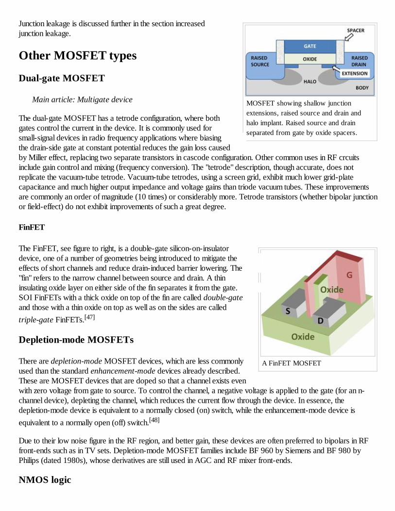
FinFET
The FinFET, see figure to right, is a double-gate silicon-on-insulatordevice, one of a number of geometries being introduced to mitigate theeffects of short channels and reduce drain-induced barrier lowering. The"fin" refers to the narrow channel between source and drain. A thininsulating oxide layer on either side of the fin separates it from the gate.SOI FinFETs with a thick oxide on top of the fin are called double-gateand those with a thin oxide on top as well as on the sides are calledtriple-gate FinFETs.[47]
Depletion-mode MOSFETs
There are depletion-mode MOSFET devices, which are less commonlyused than the standard enhancement-mode devices already described.These are MOSFET devices that are doped so that a channel exists evenwith zero voltage from gate to source. To control the channel, a negative voltage is applied to the gate (for an n-channel device), depleting the channel, which reduces the current flow through the device. In essence, thedepletion-mode device is equivalent to a normally closed (on) switch, while the enhancement-mode device isequivalent to a normally open (off) switch.[48]
Due to their low noise figure in the RF region, and better gain, these devices are often preferred to bipolars in RFfront-ends such as in TV sets. Depletion-mode MOSFET families include BF 960 by Siemens and BF 980 byPhilips (dated 1980s), whose derivatives are still used in AGC and RF mixer front-ends.
NMOS logic
Cross section of a PowerMOSFET, with square cells. Atypical transistor is constituted ofseveral thousand cells
n-channel MOSFETs are smaller than p-channel MOSFETs and producing only one type of MOSFET on a siliconsubstrate is cheaper and technically simpler. These were the driving principles in the design of NMOS logic whichuses n-channel MOSFETs exclusively. However, unlike CMOS logic, NMOS logic consumes power even whenno switching is taking place. With advances in technology, CMOS logic displaced NMOS logic in the mid-1980sto become the preferred process for digital chips.
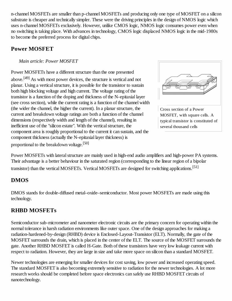
Power MOSFET
Main article: Power MOSFET
Power MOSFETs have a different structure than the one presentedabove.[49] As with most power devices, the structure is vertical and notplanar. Using a vertical structure, it is possible for the transistor to sustainboth high blocking voltage and high current. The voltage rating of thetransistor is a function of the doping and thickness of the N-epitaxial layer(see cross section), while the current rating is a function of the channel width(the wider the channel, the higher the current). In a planar structure, thecurrent and breakdown voltage ratings are both a function of the channeldimensions (respectively width and length of the channel), resulting ininefficient use of the "silicon estate". With the vertical structure, thecomponent area is roughly proportional to the current it can sustain, and thecomponent thickness (actually the N-epitaxial layer thickness) isproportional to the breakdown voltage.[50]
Power MOSFETs with lateral structure are mainly used in high-end audio amplifiers and high-power PA systems.Their advantage is a better behaviour in the saturated region (corresponding to the linear region of a bipolartransistor) than the vertical MOSFETs. Vertical MOSFETs are designed for switching applications.[51]
DMOS
DMOS stands for double-diffused metal–oxide–semiconductor. Most power MOSFETs are made using thistechnology.
RHBD MOSFETs
Semiconductor sub-micrometer and nanometer electronic circuits are the primary concern for operating within thenormal tolerance in harsh radiation environments like outer space. One of the design approaches for making aradiation-hardened-by-design (RHBD) device is Enclosed-Layout-Transistor (ELT). Normally, the gate of theMOSFET surrounds the drain, which is placed in the center of the ELT. The source of the MOSFET surrounds thegate. Another RHBD MOSFET is called H-Gate. Both of these transistors have very low leakage current withrespect to radiation. However, they are large in size and take more space on silicon than a standard MOSFET.
Newer technologies are emerging for smaller devices for cost saving, low power and increased operating speed.The standard MOSFET is also becoming extremely sensitive to radiation for the newer technologies. A lot moreresearch works should be completed before space electronics can safely use RHBD MOSFET circuits ofnanotechnology.

When radiation strikes near the silicon oxide region (STI) of the MOSFET, the channel inversion occurs at thecorners of the standard MOSFET due to accumulation of radiation induced trapped charges. If the charges arelarge enough, the accumulated charges affect STI surface edges along the channel near the channel interface (gate)of the standard MOSFET. Thus the device channel inversion occurs along the channel edges and the device createsoff-state leakage path, causing device to turn on. So the reliability of circuits degrades severely. The ELT offersmany advantages. These advantages include improvement of reliability by reducing unwanted surface inversion atthe gate edges that occurs in the standard MOSFET. Since the gate edges are enclosed in ELT, there is no gateoxide edge (STI at gate interface), and thus the transistor off-state leakage is reduced very much.
Low-power microelectronic circuits including computers, communication devices and monitoring systems in spaceshuttle and satellites are very different from what we use on earth. They are radiation (high-speed atomic particleslike proton and neutron, solar flare magnetic energy dissipation in earth's space, energetic cosmic rays like X-ray,gamma ray etc.) tolerant circuits. These special electronics are designed by applying very different techniques usingRHBD MOSFETs to ensure the safe space journey and also space-walk of astronauts.
MOSFET analog switch
MOSFET analog switches use the MOSFET to pass analog signals when on, and as a high impedance when off.Signals flow in both directions across a MOSFET switch. In this application, the drain and source of a MOSFETexchange places depending on the relative voltages of the source/drain electrodes. The source is the more negativeside for an N-MOS or the more positive side for a P-MOS. All of these switches are limited on what signals theycan pass or stop by their gate–source, gate–drain and source–drain voltages; exceeding the voltage, current, orpower limits will potentially damage the switch.
Single-type MOSFET switch
This analog switch uses a four-terminal simple MOSFET of either P or N type.
In the case of an n-type switch, the body is connected to the most negative supply (usually GND) and the gate isused as the switch control. Whenever the gate voltage exceeds the source voltage by at least a threshold voltage,the MOSFET conducts. The higher the voltage, the more the MOSFET can conduct. An N-MOS switch passesall voltages less than Vgate–Vtn. When the switch is conducting, it typically operates in the linear (or ohmic) modeof operation, since the source and drain voltages will typically be nearly equal.
In the case of a P-MOS, the body is connected to the most positive voltage, and the gate is brought to a lowerpotential to turn the switch on. The P-MOS switch passes all voltages higher than Vgate–Vtp (threshold voltage Vtpis negative in the case of enhancement-mode P-MOS).
A P-MOS switch will have about three times the resistance of an N-MOS device of equal dimensions becauseelectrons have about three times the mobility of holes in silicon.
Dual-type (CMOS) MOSFET switch
This "complementary" or CMOS type of switch uses one P-MOS and one N-MOS FET to counteract thelimitations of the single-type switch. The FETs have their drains and sources connected in parallel, the body of theP-MOS is connected to the high potential (VDD) and the body of the N-MOS is connected to the low potential(Gnd). To turn the switch on, the gate of the P-MOS is driven to the low potential and the gate of the N-MOS is
driven to the high potential. For voltages between VDD–Vtn and Gnd–Vtp, both FETs conduct the signal; forvoltages less than Gnd–Vtp, the N-MOS conducts alone; and for voltages greater than VDD–Vtn, the P-MOSconducts alone.
The voltage limits for this switch are the gate–source, gate–drain and source–drain voltage limits for both FETs.Also, the P-MOS is typically two to three times wider than the N-MOS, so the switch will be balanced for speedin the two directions.
Tri-state circuitry sometimes incorporates a CMOS MOSFET switch on its output to provide for a low-ohmic, full-range output when on, and a high-ohmic, mid-level signal when off.
See also
BSIMHigh electron mobility transistor (HEMT)Polysilicon depletion effectTransistor model
References
1. ^ Yuhua Cheng, Chenming Hu (1999). "§2.1 MOSFET classification and operation"(http://books.google.com/books?id=R5DP56qUql4C&pg=PA13). MOSFET modeling & BSIM3 user's guide.Springer. p. 13. ISBN 0-7923-8575-6.
2. ^ U.A.Bakshi, A.P.Godse (2007). "§8.2 The depletion mode MOSFET" (http://books.google.com/books?id=ggpVToC2obIC&pg=SA8-PA2#v=onepage&q&f=false). Electronic Circuits. Technical Publications. pp. 8–2.ISBN 978-81-8431-284-3.
3. ^ "Intel 45nm Hi-k Silicon Technology" (http://www.intel.com/technology/architecture-silicon/45nm-core2/index.htm).
4. ^ Electronic Circuit Symbols (http://www.circuitstoday.com/electronic-circuit-symbols)5. ^ IEEE 3156. ^ Microelectronic Circuit Design (http://highered.mcgraw-
hill.com/sites/dl/free/0073191639/366537/Chapter_4.pdf#page=19), Jaeger, Blalock - Figure 4.15 IEEE StandardMOS transistor circuit symbols.
7. ^ "Using a MOSFET as a Switch" (http://brunningsoftware.co.uk/FET.htm). 090507 brunningsoftware.co.uk8. ^ This model was introduced by H Shichman and DA Hodges (1968). "Modeling and simulation of insulated-gate
field-effect transistor switching circuits" (http://ieeexplore.ieee.org/xpl/articleDetails.jsp?arnumber=1049902).IEEE Journal of Solid-state circuits SC–3: 285–289. doi:10.1109/JSSC.1968.1049902(http://dx.doi.org/10.1109%2FJSSC.1968.1049902). and often is called the Shichman-Hodges model.
9. ^ For example, see Yuhua Cheng, Chenming Hu (1999). MOSFET modeling & BSIM3 user's guide(http://books.google.com/books?id=R5DP56qUql4C&source=gbs_navlinks_s). Springer. ISBN 0-7923-8575-6..The most recent version of the BSIM model is described in Sriramkumar V., Navid Paydavosi,Darsen Lu, Chung-Hsun Lin,Mohan Dunga, Shijing Yao, Tanvir Morshed,Ali Niknejad, and Chenming Hu (2012). "BSIM-CMG106.1.0beta Multi-Gate MOSFET Compact Model" (http://www-device.eecs.berkeley.edu/bsim/Files/BSIMCMG/BSIMCMG106.0.0/BSIMCMG106.0.0_TechnicalManual_20120313.pdf). Department of EE and CS, UC Berkeley. Retrieved 2012-04-01.
10. ^ P R Gray, P J Hurst, S H Lewis, and R G Meyer (2001). Analysis and Design of Analog Integrated Circuits(http://worldcat.org/isbn/0471321680) (Fourth Edition ed.). New York: Wiley. pp. 66–67. ISBN 0-471-32168-0.
11. ^ P. R. van der Meer, A. van Staveren, A. H. M. van Roermund (2004). Low-Power Deep Sub-Micron CMOSLogic: Subthreshold Current Reduction (http://books.google.com/books?id=nyken8ivkb8C&pg=PA78&dq=weak+inversion&sig=SwYg44W-tRbG1cSjQBemdM22PgU). Dordrecht:
id=nyken8ivkb8C&pg=PA78&dq=weak+inversion&sig=SwYg44W-tRbG1cSjQBemdM22PgU). Dordrecht:Springer. p. 78. ISBN 1-4020-2848-2.
12. ^ Degnan, Brian. "Wikipedia fails subvt" (https://sites.google.com/site/degnan68k/semiconductors/wikipedia-fails-subvt).
13. ^ Mead, Carver (1989). Analog VLSI and Neural Systems. Reading, MA: Addison-Wesley. p. 370.ISBN 9780201059922.
14. ^ Leslie S. Smith, Alister Hamilton (1998). Neuromorphic Systems: Engineering Silicon from Neurobiology(http://books.google.com/books?id=kWSXEHyQL9sC&pg=PA55&dq=subthreshold+%22+current+mirror%22&as_brr=0&sig=SklZWp6j9atrSzuvn9cbW37udMo#PPA52,M1). World Scientific. pp. 52–56. ISBN 981-02-3377-9.
15. ^ Satish Kumar (2004). Neural Networks: A Classroom Approach (http://books.google.com/books?id=GJQh-2p6TvgC&pg=PA688&dq=neuromorphic+%22subthreshold+MOS%22&as_brr=0&sig=kCr306oIZOqnx49D4Sbf5PUJay0). Tata McGraw-Hill. p. 688. ISBN 0-07-048292-6.
16. ^ Manfred Glesner, Peter Zipf, Michel Renovell (2002). Field-programmable Logic and Applications: 12thInternational Conference (http://books.google.com/books?id=fneXs6IY2-oC&pg=PA425&dq=analog+array+subthreshold&as_brr=0&sig=pZhV3OYe7YSvlwiF7DfmVj2Ir0w). Dordrecht:Springer. p. 425. ISBN 3-540-44108-5.
17. ^ Eric A. Vittoz (1996). "The Fundamentals of Analog Micropower Design" (http://books.google.com/books?id=WTInL9njOKAC&pg=PA367&dq=weak-inversion+maximum+transconductance&as_brr=3&ei=o_OpSoSGN5XgNfO3vYgK#v=onepage&q=weak-inversion%20maximum%20transconductance&f=false). In Chris Toumazou, Nicholas C. Battersby, and SoniaPorta. Circuits and systems tutorials. John Wiley and Sons. pp. 365–372. ISBN 978-0-7803-1170-1.
18. ^ Sandeep K. Shukla, R. Iris Bahar (2004). Nano, Quantum and Molecular Computing(http://books.google.com/books?id=lLvo1iMGhJgC&pg=PA10&dq=subthreshold+%22process+variation%22&as_brr=0&sig=-oK8URqQwvDqmxjr7V4bhuOBtS4). Springer. p. 10 and Fig. 1.4, p. 11. ISBN 1-4020-8067-0.
19. ^ Ashish Srivastava, Dennis Sylvester, David Blaauw (2005). Statistical Analysis and Optimization For VLSI:Timing and Power (http://books.google.com/books?id=WqsQTyOu5jwC&pg=PA9&dq=%22variation+in+leakage+current%22&as_brr=0&sig=6cHT1H0G-PnNvk0bE7zPYViDSjU#PPA135,M1). Springer. p. 135. ISBN 0-387-25738-1.
20. ^ C Galup-Montoro & Schneider MC (2007). MOSFET modeling for circuit analysis and design(http://worldcat.org/isbn/981-256-810-7). London/Singapore: World Scientific. p. 83. ISBN 981-256-810-7.
21. ^ Norbert R Malik (1995). Electronic circuits: analysis, simulation, and design (http://worldcat.org/isbn/0-02-374910-5). Englewood Cliffs, NJ: Prentice Hall. pp. 315–316. ISBN 0-02-374910-5.
22. ^ PR Gray, PJ Hurst, SH Lewis & RG Meyer. §1.5.2 p. 45 (http://worldcat.org/isbn/0-471-32168-0). ISBN 0-471-32168-0.
23. ^ A. S. Sedra and K.C. Smith (2004). Microelectronic circuits (http://worldcat.org/isbn/0-19-514251-9) (FifthEdition ed.). New York: Oxford. p. 552. ISBN 0-19-514251-9.
24. ^ A. S. Sedra and K.C. Smith. p. 250, Eq. 4.14 (http://worldcat.org/isbn/0-19-514251-9). ISBN 0-19-514251-9.25. ^ For a uniformly doped p-type substrate with bulk acceptor doping of NA per unit volume,
with ni the intrinsic mobile carrier density per unit volume in the bulk. See, for example, Narain Arora (2007)."Equation 5.12" (http://books.google.com/books?id=SkT2xOuvpuYC&pg=PA173). Mosfet modeling for VLSIsimulation: theory and practice. World Scientific. p. 173. ISBN 981-256-862-X.
26. ^ "Body effect" (http://equars.com/~marco/poli/phd/node20.html). Equars.com. Retrieved 2012-06-02.27. ^ "1960 – Metal Oxide Semiconductor (MOS) Transistor Demonstrated: John Atalla and Dawon Kahng fabricate
working transistors and demonstrate the first successful MOS field-effect amplifier (U.S. Patent 3,102,230 filed in1960, issued in 1963)" (http://www.computerhistory.org/semiconductor/timeline/1960-MOS.html).
28. ^ "The Silicon Engine | 1948 – Conception of the Junction Transistor"(http://www.computerhistory.org/semiconductor/timeline/1948-conception.html). Computer History Museum.2007.
29. ^ "Computer History Museum – The Silicon Engine | 1955 – Photolithography Techniques Are Used to Make
29. ^ "Computer History Museum – The Silicon Engine | 1955 – Photolithography Techniques Are Used to MakeSilicon Devices" (http://www.computerhistory.org/semiconductor/timeline/1955-Photolithography.html).Computerhistory.org. Retrieved 2012-06-02.
30. ^ Robert H. Cushman. "2-1/2-generation μP's-$10 parts that perform like low-end mini's"(http://www.swtpc.com/mholley/Microprocessors/EDN_Sep_20_1975_6502.pdf). EDN September 20 1975.
31. ^ "Computer History Museum – The Silicon Engine | 1963 – Complementary MOS Circuit Configuration isInvented" (http://www.computerhistory.org/semiconductor/timeline/1963-CMOS.html). Computerhistory.org.Retrieved 2012-06-02.
32. ^ "Computer History Museum – Exhibits – Microprocessors"(http://www.computerhistory.org/microprocessors/). Computerhistory.org. Retrieved 2012-06-02.
33. ^ "International Technology Roadmap for Semiconductors" (http://www.itrs.net).34. ^ "1965 – "Moore's Law" Predicts the Future of Integrated Circuits"
(http://www.computerhistory.org/semiconductor/timeline/1965-Moore.html). Computer History Museum.35. ^ Kaushik Roy, Kiat Seng Yeo (2004). Low Voltage, Low Power VLSI Subsystems
(http://books.google.com/books?id=jXm4pNxCSCYC&printsec=frontcover&dq=subthreshold+mosfet+%22static+power%22&as_brr=0&sig=gr4ovBNlI9i-IafjcoHio7vmvpQ#PPA44,M1). McGraw-Hill Professional. Fig. 2.1, p. 44. ISBN 0-07-143786-X.
36. ^ Kaushik Roy, Kiat Seng Yeo (2004). Low Voltage, Low Power VLSI Subsystems(http://books.google.com/books?id=jXm4pNxCSCYC&pg=PA4&dq=Energy+switching+%22ITRS+Projection%22&as_brr=0&sig=OSs1R-OzbVgLa_4pC0do1pkaZeo). McGraw-Hill Professional. Fig. 1.1, p. 4. ISBN 0-07-143786-X.
37. ^ Dragica Vasileska, Stephen Goodnick (2006). Computational Electronics (http://books.google.com/books?id=DBPnzqy5Fd8C&pg=PA103&dq=MOSFET+half+%22+total+power+consumption%22&as_brr=0&sig=DVaR6DvP9YxlNQSwcyvTgwpum3s). Morgan & Claypool. p. 103. ISBN 1-59829-056-8.
38. ^ "Frontier Semiconductor Paper" (http://frontiersemi.com/pdf/papers/RsLransist.pdf) (PDF). Retrieved 2012-06-02.
39. ^ Wai-Kai Chen (2006). The VLSI Handbook (http://books.google.com/books?id=NDdsjtTLTd0C&pg=PT49&lpg=PT49&dq=halo+%22junction+leakage%22&source=web&ots=a-sCYYSP0k&sig=ZvFajEiopwY89nT05YTmX114Lf4#PPT49,M1). CRC Press. Fig. 2.28, p. 2–22. ISBN 0-8493-4199-X.
40. ^ A Comparison Of Spike, Flash, Sper and Laser Annealing For 45nm CMOS:http://www.mrs.org/s_mrs/sec_subscribe.asp?CID=2593&DID=109911&action=detail
41. ^ VLSI wiring capacitance (http://www.research.ibm.com/journal/rd/293/ibmrd2903G.pdf). IBM Journal ofResearch and Development.
42. ^ D Soudris, P Pirsch, E Barke (Editors) (2000). Integrated Circuit Design: Power and Timing Modeling,Optimization, and Simulation (10th Int. Workshop) (http://books.google.com/books?id=TGQxMLsGzVUC&pg=PA38&lpg=PA38&dq=%22wiring+capacitance%22&source=web&ots=LTtgLKbRWu&sig=jTNMBOyqtBpgkD7JbodM2YQ0TI8). Springer. p. 38. ISBN 3-540-41068-6.
43. ^ Michael Orshansky, Sani Nassif, Duane Boning (2007). Design for Manufacturability And Statistical Design: AConstructive Approach (http://www.amazon.com/gp/reader/0387309284/ref=sib_dp_pt/002-1766819-0058402#reader-link). New York 309284: Springer.
44. ^ http://www.revera.com/VeraFlex/hkmg_approaches.htm45. ^ Jean-Pierre Colinge, Cynthia A. Colinge (2002). Physics of Semiconductor Devices
(http://books.google.com/books?id=ZcDE-ENKh2gC&pg=PA233&dq=halo+MOSFET&as_brr=0&sig=q_IW6haw9G9-rBh9E_d-i7rDbFc). Dordrecht:Springer. p. 233, Figure 7.46. ISBN 1-4020-7018-7.
46. ^ Eicke R. Weber, Jarek Dabrowski (Editors) (2004). Predictive Simulation of Semiconductor Processing: Statusand Challenges (http://books.google.com/books?id=oCH9tiY7VeoC&pg=PA5&dq=MOSFET+%22raised+source%22&as_brr=0&sig=61g3_KAMiwEtaSq_zKnt6JPqJjo). Dordrecht: Springer. p. 5, Figure 1.2. ISBN 3-540-20481-4.
47. ^ See, for example, PM Zeitzoff, JA Hutchby, HR Huff (2002). "Figure 12: Simplified cross section of FinFETdouble-gate MOSFET." (http://books.google.com/books?id=uC6h4-OEWsMC&pg=PA82). In Yoon-Soo Park,Michael Shur, William Tang, eds. Frontiers in electronics: future chips : proceedings of the 2002 Workshop onFrontiers in Electronics (WOFE-02), St Croix, Virgin Islands, USA, 6–11 January 2002. World Scientific. p. 82.
Frontiers in Electronics (WOFE-02), St Croix, Virgin Islands, USA, 6–11 January 2002. World Scientific. p. 82.ISBN 981-238-222-4. and J-H Lee, J-W Lee, H-A-R Jung and B-K Choi (2009). "Comparison of SOI FinFETs andbulk FinFETs: Figure 2" (http://books.google.com/books?id=OVbb42PwZysC&pg=PA102). Silicon-on-InsulatorTechnology and Devices. The Electrochemical Society. p. 102. ISBN 1-56677-712-7.
48. ^ Techweb (http://www.techweb.com/encyclopedia/imageFriendly.jhtml;?term=depletion+mode). Techweb(2010-01-29). Retrieved on 2010-11-27.
49. ^ Power Semiconductor Devices, B. Jayant Baliga, PWS publishing Company, Boston. ISBN 0-534-94098-650. ^ Power MOSFET Basics: Understanding MOSFET Characteristics Associated With The Figure of Merit
(http://www.element-14.com/community/docs/DOC-18273/l/power-mosfet-basics-understanding-mosfet-characteristics-associated-with-the-figure-of-merit). element14. Retrieved on 2010-11-27.
51. ^ Power MOSFET Basics: Understanding Gate Charge and Using It To Assess Switching Performance(http://www.element-14.com/community/docs/DOC-18275/l/power-mosfet-basics-understanding-gate-charge-and-using-it-to-assess-switching-performance). element14. Retrieved on 2010-11-27.
External links
Understanding power MOSFET data sheet parameters - NXP PDF Application Note AN11158(http://www.nxp.com/documents/application_note/AN11158.pdf)An introduction to depletion-mode MOSFETs (http://www.automotivedesignline.com/showArticle.jhtml;?articleID=191900470)Power MOSFETs (http://www.alpha-europe.de/microelectronics-products/dmos-transistors/)Criteria for Successful Selection of IGBT and MOSFET Modules(http://www.powerguru.org/2012/04/15/criteria-for-a-successful-selection-of-igbt-and-mosfet-modules/)MOSFET Process Step by Step(http://www.ece.byu.edu/cleanroom/virtual_cleanroom.parts/MOSFETProcess.html) A Flash slide showingthe fabricating process of a MOSFET in detail stepMOSFET Calculator (http://www.ece.byu.edu/cleanroom/MOSFET_calc.phtml) MOSFET CalculatorAdvanced MOSFET Issues Advanced MOSFET issues(http://ecee.colorado.edu/~bart/book/book/chapter7/ch7_7.htm#7_7_7). ecee.colorado.edu. Retrieved on2010-11-27.MOSFET applet (http://www-g.eng.cam.ac.uk/mmg/teaching/linearcircuits/mosfet.html) Very nice appletthat helps to understand MOSFET.Dr. Ulrich Nicolai, Dr. Tobias Reimann, Prof. Jürgen Petzoldt, Josef Lutz: Application Manual IGBT andMOSFET Power Modules, 1. Edition, ISLE Verlag, 1998, ISBN 3-932633-24-5 PDF-Version(http://www.semikron.com/skcompub/en/application_manual-193.htm)Wintrich, Arendt; Nicolai, Ulrich; Tursky, Werner; Reimann, Tobias (2011). [PDF-Version(http://www.powerguru.org/wordpress/wp-content/uploads/2012/12/SEMIKRON_application_manual_power_semiconductors.pdf) ApplicationManual 2011] (2nd ed.). Nuremberg: Semikron. ISBN 978-3-938843-66-6.MIT OpenCourseWare courses:
MIT Open Courseware 6.002 – Spring 2007 (http://ocw.mit.edu/OcwWeb/Electrical-Engineering-and-Computer-Science/6-002Spring-2007/CourseHome/index.htm) – Link to the intro electricalengineering course at MIT on circuits and electronics.MIT Open Courseware 6.012 – Fall 2009 (http://ocw.mit.edu/courses/electrical-engineering-and-computer-science/6-012-microelectronic-devices-and-circuits-fall-2009/) – Link to a more advancedclass taught at MIT all about microelectronics and MOSFETs
Georgia Tech BJT and FET Slides (http://users.ece.gatech.edu/~alan/index_files/ECE3040Lecture.htm)
Slides from a Microelectronic Circuits class at Georgia TechCircuitDesign: MOS Diffusion Parasitics (http://www.circuitdesign.info/blog/2008/12/mos-diffusion-parasitics/) Crude illustrations of MOS diffusion structure and sample circuit layouts to minimize theirparasiticsCourse on Physics of Nanoscale Transistors (http://nanohub.org/resources/5306)Notes on Ballistic MOSFETs by Dr. Lundstrom (http://nanohub.org/resources/489) – theory of ballisticMOSFETs.Veendrick, Harry J. M. (2008). Nanometer CMOS ICs, from Basics to ASICs. New York: Springer.p. 770. ISBN 978-1-4020-8332-7.
Retrieved from "http://en.wikipedia.org/w/index.php?title=MOSFET&oldid=606571113"Categories: Transistor types
This page was last modified on 1 May 2014 at 03:11.Text is available under the Creative Commons Attribution-ShareAlike License; additional terms may apply.By using this site, you agree to the Terms of Use and Privacy Policy. Wikipedia® is a registered trademarkof the Wikimedia Foundation, Inc., a non-profit organization.