mos transistor model and layout issuesmos transistor model and layout issues one of the most...
TRANSCRIPT
Chapter II MOS Transistor Modelling for MMW Circuits
15
Chapter Chapter Chapter Chapter IIIIIIII
MOS transistor model and layout issues
One of the most important design issues in millimeter wave circuit design in modern MOS
technologies is active devices and related parasitic elements modeling. The MOS transistor
model that can be used in such high frequency must accurately comprise all of the unwanted
parasitic effects that arise in high frequencies, as well as DC and low frequency
characteristics.
Professional circuit simulators and foundry design kits provide a complete environment for
design, optimization and validation of different circuits, as well as layout tools. However due
to many high frequency effects that arises in millimeter wave frequencies and have not been
included in available RF design kits, millimeter wave circuit designers need to develop an
individual simple design tool. This tools are used in pre-design analysis, design procedure and
after-design diagnosis. Then the foundry design kit is used for final design evaluation and
probably optimization, after some special considerations by the designer.
In our work the problem is more sever, since the foundry design kit we are working with,
is for 90 nm digital CMOS technology and does not provides any RF design facilities.
Consequently we are obligated to develop our design and optimization tools, using the
foundry design kit data and the foundry confidential Design Rule Manual (DRM). Then we
should use the design kit with some special considerations for post-layout simulation and to
evaluate the final design. Off course the parasitic extraction tools of the design kit are not
useful for our work. An accurate model for MOS transistor is one the most important
requirement of our design and optimization tool.
In the STMicroelectronics 90nm global purpose CMOS foundry design kit, BSIM3v3 has
been used with some modifications, specially to capture the stress effect [1], [2], [3]. The
modifications have been mainly made as pre-calculation of some BSIM3v3 standard
parameters. However this model is not sufficient for millimeter wave design and hence we
obligatory should develop an accurate model based on the design kit model and the used
technology data, given in the foundry Design Rule Manual (DRM). The parts of our model
that have been covered by the ST foundry design kit, have been calibrate using the design kit.
The other parts have been obtained analytically, using the foundry design rule manual.
In this chapter we will give a brief overview of available models. Then we will describe
our model that we have used in our design and optimization tool. Our model consists of some
new equations for I-V characteristics, gate resistance, substrate and layout-dependent effects.
We also will propose an analytic method for layout optimization. Our model consists of the
following main sections:
� Transistor core model, consisting of single equation I-V model, capacitance model, small
signal and noise models
� Layout-dependent parasitic elements, consisting of gate resistance model, substrate model,
interconnect model and other parasitic elements.
� Y parameter model for small signal and noise analysis
II.1 MOS Modeling Overview In recent years the MOS technology has been scaled down to nanometer regime and various
MOS transistor models have been proposed to best capture the transistor behavior. MOS
modeling is always a compromise between two factors: Accuracy and complexity. In a
glance, all of the available models can be divided in to two main categories. First category is

Chapter II MOS Transistor Modelling for MMW Circuits
16
the table-based or table-look-up models, directly obtained from measurement results. Second
category is the mathematical model that is fully or partially obtained from the study of the
physics of the transistor. In other glance, all of the models can be divided in to simple or
complicated models. Simple models are used in small primary design tools and are useful in
pre-design analysis and after-design diagnosis. These models can give an insight of the
behavior of the device, as well as the effect of the device parameters on the final design.
These models are also useful for education purposes. Complicated models are used in
professional circuit simulators for design evaluation and optimization.
Here we divide all of the models in to three categories:
� Professional physical models
� Professional table-based models
� Simple physical models
II.1.1 Professional Physical Models
These models have been developed based on the accurate study of the related physical
phenomena’s. In nanometer scale MOS technologies, these phenomena’s, specially short
channel and quantum effects, are very complicated and hence such models are very
complicated. Three main groups of these models have been developed for modern MOS
technologies [4], [5]. First and more extended group is based on the threshold voltage. Spice
models, Bsim3, BSIM4 and MM9 are examples of this group [6], [7], [8]. Second group is
based on the inversion charge approach. EKV [5], ACM1 [9] and BSIM5 [10] are based on
the inversion charge or charge sheet layer methods. Third group are surface-potential-based
models. SP [11], PSP [12] and MM11 [13] are the examples of these models. Two last groups
are more adapted to the nanometer regime MOS technologies, since threshold voltage based
models use many mathematical smoothing functions and fitting parameters, and hence less
physical insight to device operation [7].
Extraction of model parameters from measurement results is very essential for professional
models [13]. Specially the parameters related to capacitance and trans-capacitance has been a
challenge from past to present [14], [15].
II.1.2 Table-Based Models
As the MOS technology goes to nanometer regime, capturing the new physical phenomena’s
makes the professional physical based models more and more complicated. Such complicated
models are computationally expensive and a greatly influence the simulation run time, so that
up to 80% of the run time is consumed to model evaluations [16]. On the other hand simple
physical models have not enough accuracy for final design evaluation and optimization. So
the table-based models have been presented to comprise both of the accuracy and simplicity.
Table based models have been developed since the 1970s, in the digital and mixed mode
circuit simulators like MOTIS [17]. Then 3D models was born in 1982 [18] and professional
circuit simulators based on these models was developed in 1983 [19]. Table base models were
applied to RF simulators by Root et al. for GaAs FET devices [20].
The accuracy of table-based models is influenced by a large number of factors, such as
extrapolation accuracy, data interpolation accuracy and the accuracy of the parameters
derived from the table data (such as ac model parameters). Data interpolation from the table
data has been discussed in [21]. In [16] different table structures have been considered to
obtain the required accuracy with minimum table size.
1 Advanced Compact MOS Model

Chapter II MOS Transistor Modelling for MMW Circuits
17
II.1.3 Simple Physical Models
Due to their complexity, professional MOS models can not be used in the simple individual
design tools. For example, MM11 has approximately 80 parameters [22]. BSIM3v3 has more
up to 80 parameters for I-V equation, 22 parameters for capacitances and 12 parameters for
thermal effects and 4 control parameters. BSIM4.3.0 has about 136 parameters for I-V model,
20 parameters for RF and layout dependent effects, 18 parameters for thermal effects and 20
control parameters, as well as some parameters for comprise the stress effect [23], [24].
Development of individual design tools need to have a simple, but accurate MOS device
model. Such model can give the designer insight of what happens physically in the device and
this helps the designer to perform the pre-design analysis and after-design diagnosis [25].
II.2 Our Model for Intrinsic MOS Transistor In this section we present a simple, but accurate model that can capture the MOS transistor
core characteristics in 90nm MOS technology. Our model consists of large signal nonlinear I-
V characteristics and capacitance models, a small signal linear model and a simple noise
model. I-V characteristic is a set of mathematical equations that describes the drain voltage as
a function of four transistor nodes, i.e. gate, drain, source and bulk. Capacitances model are
mathematical equations that describe the nodal capacitance and trans-capacitance of the
transistor nodes. I-V and capacitance models are directly used in DC or large signal analysis,
as well as in the small signal analysis to calculate the small signal model parameters.
Continuity of the large signal equations and their derivatives are very important in simulation
convergence [26]. So in our model all of large signal equations are unique for both of linear
and saturation regions.
II.2.1 I-V Characteristic
The fist ideas in modeling of I-V characteristics of a MOS transistor stems from Shockley
studies [27]. Then the basic quadratic equation derived in early 1960 [28]. This equation is as
follows:
( )
( )
−
−−=
regionsaturationVVL
WC
regionlinearVVVVL
WC
cutoff
I
thgoxn
ddthgoxnd
2
0
µ
µ (II-1)
where Vth is the threshold voltage. For many years, this basic model has been recognized as
inadequate and various modifications have been made to fit the basic equation on the modern
MOS technologies. Mobility reduction, velocity saturation and channel length modulation are
examples of the performed modifications. In the saturation region channel length modulation
can be considered simply as:
( )( )effdsodox
ds VVVL
WCI −+= λ
µ12 (II-2)
Where Vod is the over drive voltage, defined as:
thgsod VVV −= (II-3)
Mobility degradation and velocity saturation have been considered in many literatures and
text books [29], [30], [31]. Mobility degradation is due to the lateral filed due to drain-source
voltage, as well as the vertical field due to gate voltage. In most of these literatures the
mobility has been considered as a average effect in the channel and hence a multiplicative
modifier has been used. The most common way is express the mobility as in [4]:

Chapter II MOS Transistor Modelling for MMW Circuits
18
( )
+++
=
LE
VVV
c
dodod 112
21
0
θθ
µµ (II-4)
Multiplicative correction of mobility value has been considered in the physical alpha-power
law model and some other physical models [32], [33]. However the field components are not
uniform in all of the channel length. The vertical field dominates in part of the channel near to
the source and reduces the mobility. However in the drain end of the channel lateral field is
dominant and causes the velocity saturation. Consequently considering a average effect can
not lead to an accurate model [4].
The nonlinear behavior of drain current has been investigated in many presented models.
Although Shockley model predicts quadratic variation of the drain current in saturation
region, this diminished in short channel MOS transistors. Alpha-power law model, presented
in 1990, was a fully empirical model that proposed a new equation as follows [34]:
( )αthgsds VVBI −= (II-5)
In [34] value of alpha was found 1.2, 1.2 and 1 for 1.2 um, 0.8 um and 0.5um technologies,
respectively. Other alpha-power low models have been developed with physical insight in to
the transistor behavior. In [32] and [35] with physical analysis of the drain current equations
have been derived to calculate the exact value of alpha, as a function of gate voltage. In [35]
has been shown that the value of alpha goes toward 2 in long channel case and goes toward 1
in short channel case.
Unfortunately none of the above models have adequate accuracy in today’s nanometer
scale MOS transistors. Consequently in recent years beside new professional complicated
models, some new simple models have been developed for design, analysis and simple
simulation tools. Hauser has proposed a physical model, based on the well known sheet
charge layer model [4]. Based on this model the drain current and the voltage along the
channel obey a simple differential equation:
( )x
VVVVWCI thgsoxds
∂
∂−−= µ (II-6)
He has used a new approach to calculate the mobility as a function of gate and drain voltages.
The obtained result is a single-equation model, well fitted to I-V characteristics of a transistor
with 90nm gate length. In [29] a compact model has been developed to calculate the trans-
conductance of a deep submicron transistor. This model predicts quadratic relation of the
drain current and gate-source voltage for small gate-source voltages and linear relation for
large gate-source voltages. Measurement results in [1] show that the drain current is linear
function of gate voltage for 0.13 um MOS technology. Simple model of Gray also shows such
behavior [31]:
12
2
0
+
=
sat
od
odoxds
LE
V
V
L
WCI
µ (II-7)
For large L drain current is quadratic function of gate voltage, and for small values of L the
function is linear.
A simple model have been developed in [1] for RF applications. This model is single-
equation for both of linear and saturation regions. The basis is Shockley model, but velocity
saturation has been included as an empirical correcting term and also channel length
modulation and vertical field effect have been considered as conventional multiplicative
terms. Another simple model has been addressed in [25], in which channel length modulation
has been considered as a function of gate voltage. In [25] has been noted that for small gate
voltages, neither their model, nor other available models are not accurate.

Chapter II MOS Transistor Modelling for MMW Circuits
19
A new theory of operation of nanometer scale MOS transistors, i.e. quasi-ballistic transport
model has been proposed in [36], instead of conventional velocity saturation theory, and a
model has been developed, based on this theory. Measurement results in [1] for sub-0.1 um
scale shows that both of velocity saturation and transport models are good for large gate
voltage, i.e. in well saturated condition. However for small gate voltages velocity saturation
model is not accurate, but the transport model is well fitted to measurement results.
Overview of available I-V models show that various models have been presented for short
channel MOS transistors. However each of available models for sub-0.1um MOS
technologies is suitable for special measurement results and there is not any conventionally
accepted model. In our knowledge, the model presented by Hauser in [4] is the most
theoretically acceptable model. However this model has some shortages, as noted in [1]. In
addition Hauser model does not capture the stress effect. Consequently we have developed
our model based on our requirements.
II.2.1.1 Our I-V model
Our single-equation model is based on the linear dependency of drain current to gate voltage
in saturation region in sub-0.1 um MOS technologies. The equation is as follows:
( )dsod
effox
ds VVL
WCI λη
µ+= 0
(II-8)
Vod is the over-drive voltage, defined in (II-3). Vth is the threshold voltage. Although complete
formulas are available in most text books, it can be calculated as a linear function of the
voltage between source and bulk nodes, Vsb [37]. We have used a second order polynomial to
calculate the threshold voltage: 2
210 sbsbthth VVVV γγ ++= (II-9)
In which 1γ and 2γ are constants. Vth0 is the threshold voltage when source-bulk voltage is
zero. The coefficient η is for capturing the mobility reduction and velocity saturation effects,
and is defined as:
dsat
ds
dsat
od V
V
V
V
2
2
1+
=η (II-10)
Vdsat is the drain-source saturation voltage. Different equations have been derived for Vdsat
[38], [39], [40]. We have used the equation of [38] has been rewritten in [39] as:
x
oddsat
VV
α= (II-11)
Where xα is a function of gate-source and gate-bulk voltages. However we found an
empirical equation to calculate xα :
0
22
0
th
odx
V
V+=
φα (II-12)
In which Vth0 is the threshold voltage when Vsb is zero, 0φ is a constant voltage, that in our
case is equal to the junction built in potential. The role ofη is soft transition from linear
region to saturation region, as well as modeling the electron mobility degradation and velocity
saturation. Regarding (II-8) and comparing it with Shockley model we can define:

Chapter II MOS Transistor Modelling for MMW Circuits
20
0 5 10 15 20
0.6
0.7
0.8
0.9
1
1.1
Number of gate fingures
dra
in c
urr
en
t (m
A)
W=10 um
0 10 20 30 40 50 60
1.8
2
2.2
2.4
2.6
2.8
3
3.2
Number of gate fingures
dra
in c
urr
en
t (m
A)
W=10 um
Fig. II-1. Ids for two value of W=10 um and W=30 um, and different finger sizes
<+
=
>
+
=
dsatds
dsatds
dsateff
dsatds
ds
dsatod
dsateff
VVVV
V
VV
V
VV
V
22
2
0
2
20
1
µµ
µµ
(II-13)
The coefficient λ denotes the channel length modulation effect. In [25] λ has been
calculated as a function of Vgs and in [37] it has been calculated as a function of Vsb.
However we found empirically that λ is function of both of Vgs and Vsb. We have adapted the
empirical equation as in below to calculate λ :
22
0
0
od
od
VV
V
+=
λλ (II-14)
V0 and0λ both are constant coefficient.
0λ is equal to the value of λ for large gate voltages.
Weff is the effective gate width and is different from the drown W, to include the effect of
fabrication process on W and to compensate the probable errors due to the stress effects and
quasi-two-dimensional assumption in BSIM3v3. To give a view of how much these effects
are important, Ids has been shown in Fig. II-1 for two value of W=10 um and W=30 um, and
different gate finger sizes These results have been obtained from the foundry design kit. We
have calculated Weff as follows:
WqN
NqW
f
f
eff
2
1
+= (II-15)
In which q1 and q2 are constants and Nf is the number of gate fingers.
To evaluate our I-V model, we have compared it with the STMicroelectronics foundry
design kit for 90nm CMOS technology. The results have been shown in Fig. II-2. This figure
clearly shows the accuracy of our model. The effect of number of gate fingers on the drain
current has been shown in Fig. II-3, for in our model in comparison with the foundry design
kit.
II.2.2 Capacitances Model
First capacitance models were derived as a function of transistor nodes voltage [41]. Then in
consequence of charge conservation and continuity problems in voltage-based models,
charge-based models were introduced [42]. Various developments of charge-based models
were presented as threshold voltage based, surface potential based, quasi static and non-quasi

Chapter II MOS Transistor Modelling for MMW Circuits
21
static models [43]-[49]. In recent years CMOS technology has scaled down to the nanometer
feature sizes. Accurate analysis of such devices should be performed considering quantum
mechanical effects [50]. Many works has been reported on the modeling of C-V characteristic
of modern CMOS transistors, based on the quantum mechanical effects [51], [52], [53].
However almost all of the available simple and professional models use charge-based
modeling [43], [12], [13], [5]. So we present a review of charge based capacitance models.
Threshold voltage based charge/capacitance models, like in BSIM3 and BSIM4 models are
very complicated and have many fitting parameters [44], [5], [6]. Surface potential based
charge/capacitance models needs to calculate the surface potential by solving the Poisson’s
equation, that needs to iterative numerical calculations [14]. Some methods have been
presented for this model in which charge-density approximation has been used, instead of
direct solving Po equations [39], [45]. Charge-sheet model is another charge-based model in
which the channel assumed as a very thin charge layer [4].
One important issue on the capacitance modeling is Non-Quasi-Static (NQS) effects. Early
charge based models were derived by Quasi-Static (QS) approach. In QS approach the time
dependent behavior of the channel charge build-up is neglected, assuming zero time for
charges to reach their steady state condition. In principle this approach is a succession of
steady state situations. However in high frequency applications the QS assumption is not valid
and the channel charge becomes an explicit function of time. A first order estimate of the
0.4 0.5 0.6 0.7 0.80
2
4
6
8
10
12
14
gate-source voltage
dra
in c
urr
en
t (m
A)
Vds=0.9
Vds=0.7
Vds=0.5
Vds=0.3
Vds=0.1
0 0.2 0.4 0.6 0.8 1
0
2
4
6
8
10
12
drain-source voltage
dra
in c
urr
en
t (m
A)
Vgs=0.35
Vgs=0.45
Vgs=0.55
Vgs=0.65
Vgs=0.75
Fig. II-2 The I-V characteristics of our model in comparison with the foundry design kit, Circle data are from
design kit.
0 5 10 15 20
0.6
0.7
0.8
0.9
1
1.1
Number of gate fingures
dra
in c
urr
en
t (m
A)
Our Model
Design Kit
W=10 um
0 10 20 30 40 50 601.6
1.8
2
2.2
2.4
2.6
2.8
3
3.2
Number of gate fingures
dra
in c
urr
en
t (m
A)
Our Model
Design Kit
W=30 um
Fig. II-3 The effect of number of gate fingers on the drain current, for in our model in comparison with the
foundry design kit, Circle data are from design kit.
Chapter II MOS Transistor Modelling for MMW Circuits
22
scale in which the NQS effect becomes noticeable is the average transit time of the carriers in
channel [48]. Many NQS models have been published, in which NQS effects for large signal
and small signal analysis have been considered [46], [47], [48], [49]. Most of these models are
very complicated and increases the simulation time up to 4 or 5 times [23]. So some
approximated and simple models, such as distributed element treating of the transistor have
been proposed [54]. In BSIM3v3 a simple physical NQS transient model has been used, based
on the Elmore equivalent circuit [55]. This simple circuit introduces the charges build-up
time, equal to the time constant of the Elmore equivalent resistance and the gate capacitance
[23]. Although bsim3v3 has been used in many professional simulators and foundry design
kits, analysis and simulation results in [48] show that this model can not accurately model the
NQS effects in high frequencies. Capacitance modeling in BSIM4.3.0 is similar to BSIM3v3.
However BSIM4 used two first order modeling for NQS effects for large signal analysis and
introduces NQS effect in small signal capacitances and trans-conductance [24]. In [26] a very
simple model has been presented. This model is fully empirical and hence is suitable for
special cases.
II.2.2.1 Our Capacitance Model
The capacitance equations in our model have been simply derived using some basic analysis
and fitting to the design kit. For zero drain-source voltage and neglecting bulk charges in
strong inversion (SI) regime [43], we have:
( )thgsoxeffeff
SI
c VVCLWQ −=0 (II-16)
And in sub-threshold (ST) region we have :
−−=
t
offthgsST
cn
VVVQQ
νexp00 (II-17)
In which Q0 is determined from technology parameters [4]. Voff is small offset voltage to
correct the threshold voltage to best fit the measurement results. n is constant between 1 and 2
and vt is the thermal voltage. These equations are not continued and hence cause problem in
calculating the capacitances. One solution is correction of equations (II-16) and (II-17) to
obtain the continuity of charge and its first derivative at Vgs=Vth. For this purpose we should
correct the first equation as:
( )
−+−=
t
off
thgsoxeffeff
SI
cn
VQVVCLWQ
νexp00 (II-18)
And to obtain the continuity of the derivative of charge at Vgs=Vth ,we should have:
=
oxeffefft
toffCLWn
QnV
νν 0ln (II-19)
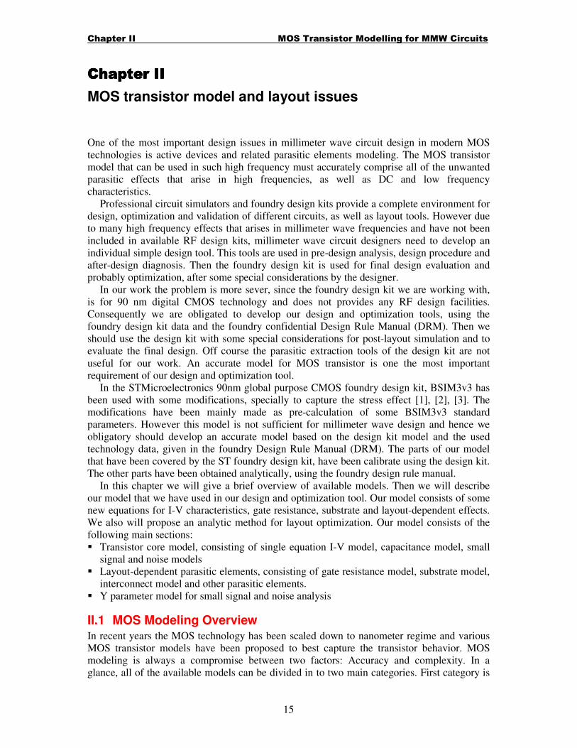
The normalized charge and its derivatives, calculated from above equations have been
depicted in Fig. II-4, in comparison with the derivative of the channel charge, obtained from
the foundry design kit. From this figure, the second derivative of the charge is not continuous
and this cause large error in calculation of capacitors. So we perform another improvement,
with defining Vgs in the strong-inversion region as follows:
p p
th
p
gsgs VVV +=′ (II-20)
And the channel charge in the strong-inversion region is calculated as:
( )
−+−′=
t
off
th
p
gsoxeffeff
SI
cn
VQVVCLWQ
νexp2 00 (II-21)
to obtain the continuity of the derivative of charge at Vgs=Vth ,we should have:

Chapter II MOS Transistor Modelling for MMW Circuits
23
=
−
p
oxeffefft
toffCLWn
QnV
11
0 2lnν
ν (II-22)
the normalized charge and its derivatives, calculated from above equations have been depicted
in Fig. II-4. In this figure the charges and the derivatives have been normalized to oxeffeff CLW
andoxC , respectively. Now the second derivative is continuous. Note that the difference
between the modified equation and the design kit result is due to the bulk charge that has not
been included in our equations.
The other approach is to use a unifying function to unify the equations (II-16) and (II-17)
into a single equation. In [39] a unifying function has been presented for soft transition from
sub-threshold to strong inversion. This unifying function has been widely used in reported
models [56], [23], [39]. Here we rewrite after introducing the small offset voltage:
−−+=
t
offthgs
toxeffeffcn
VVVnCLWQ
νν exp1ln0 (II-23)
This function goes to (II-16) for large Vgs and has semi-exponential increase for small Vgs.
Fig. II-5 shows this function and its first derivative, normalized to oxeffeff CLW and oxC ,
respectively, in comparison with the exponential equation of (II-17). The effect of Voff has
been shown in this figure. From this figure unified equation (II-23) has very good agreement
with both of equations (II-16) and (II-17). Due to its accuracy, as well as single equation
property, we use it in our model.
A) Vds Effect on the Channel Charge
Now the effect of Vds in the channel charge should be included. For this purpose we use
proper approximations separately in linear and saturation regions, and then we will unify the
obtained equations to obtain our single-equation channel charge model.
In the linear region we assume that the channel charge density linearly reduces from source to
drain, due to drain voltage. So we have:
==
==
dsatdsc
linc
dsclinc
VVQ
Q
VQQ
2
0
0_
0_
(II-24)
To express this in a single equation we use:
dsat
dsdsatclinc
V
VVQQ
2
20_
−= (II-25)
However this equation is valid in the linear region, so we should restrict Vds to this region. To
do so, we define the voltages:
dsdsds
dsat
q q
dsat
q
dsds
VVV
VVVV
′−=′′
−+=′ (II-26)
where q is a fix parameter and Vdsat is drain-source saturation voltage and was calculated in
(II-11), however here we use other equation for it, that is consistent with (II-11), but is more
soft function.
( )
−+= ∞
offgsdsat VVkV
V tanh12
(II-27)
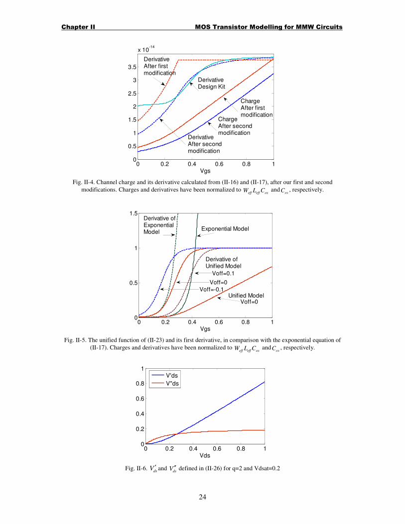
Chapter II MOS Transistor Modelling for MMW Circuits
24
0 0.2 0.4 0.6 0.8 10
0.5
1
1.5
2
2.5
3
3.5
x 10-14
Vgs
ChargeAfter firstmodification
ChargeAfter secondmodification
DerivativeAfter firstmodification
DerivativeAfter secondmodification
DerivativeDesign Kit
Fig. II-4. Channel charge and its derivative calculated from (II-16) and (II-17), after our first and second
modifications. Charges and derivatives have been normalized to oxeffeff CLW and
oxC , respectively.
0 0.2 0.4 0.6 0.8 10
0.5
1
1.5
Vgs
Unified Model
Exponential Model
Derivative ofExponentialModel
Derivative ofUnified Model
Voff=0
Voff=-0.1
Voff=0.1
Voff=0
Fig. II-5. The unified function of (II-23) and its first derivative, in comparison with the exponential equation of
(II-17). Charges and derivatives have been normalized to oxeffeff CLW and
oxC , respectively.
0 0.2 0.4 0.6 0.8 10
0.2
0.4
0.6
0.8
1
Vds
V'ds
V"ds
Fig. II-6. dsV ′ and
dsV ′′ defined in (II-26) for q=2 and Vdsat=0.2
Chapter II MOS Transistor Modelling for MMW Circuits
25
∞V is the saturation voltage for very large gate voltages and k is constant and Voff is constant
offset voltage. dsV ′ and dsV ′′ have been shown in Fig. II-6 for q=2. So to restrict Vds in (II-25) to
linear region we rewrite (II-25) as:
dsat
dsdsatclinc
V
VVQQ
2
20_
′′−= (II-28)
In saturation, for long channel devices Vds has no considerable effect on the channel charge.
However in the case of short channel devices the effect must be considered. For this purpose
we have used very simple model. Neglecting the charge density of pinched off part of the
channel, in comparison with the channel charge density in strong inversion we deduce:
−=
L
xLQQ lincsatc __ (II-29)
In which x is the length of pinched off part of the channel, that clearly shows the channel
length modulation effect. L is the channel length. x is a function of nodes voltages is a
function of channel charge, drain-source voltage and saturation voltage, Vdsat [40]. We have
calculated it as:
( )
0c
dsatds
Q
VVfx
−= (II-30)
Qc0 in the denominator steams intuitively from decreasing the channel length modulation with
increasing the channel charge. We found the approximation of the function f as below, off
adequate accuracy:
( ) ( )
>−+−
=
<=
dsatds
c
dsatdsdsatds
dsatds
VVQ
VVVVx
VVx
0
2
11
0
λλ (II-31)
Vdsat is the drain saturation voltage, defined in (II-27), λ1 and λ2 are constant parameters and
Qc0 is calculated from(II-23). With using dsV ′ defined in (II-26) instead of Vds, we can unify
(II_31) as:
( )
0
2
21
c
dsds
Q
VVx
′+′=
λλ (II-32)
Finally our single equation channel charge model obtained as follows:
−=
L
xLQQ lincc _ (II-33)
In which Qc_lin and x are calculated from (II-28) and (II-32), respectively.
B) Bulk Charge and Junction Capacitance Models
In the case of NMOS transistor for large negative gate voltages, the bulk charge increases
linearly with decreasing the gate voltage (being more negative). This is the accumulation
phase and starts from a special threshold that we denote it as accumulation threshold, Vac. On
the other hand for large positive gate voltages (strong inversion region) the bulk charge is
constant, at its minimum value. For the voltages between Vth and Vac the depleted region is
increased with increasing the gate voltage and hence the bulk charge decreases. However in
this phase the charge reduction rate is smaller than that of accumulation phase. These three
phases have been shown in the measurement and simulation data in different works [57], [45],
[44], [39], [15].
Based on the above three phases we have used the empirical equation as below to calculate
the bulk charge:
Chapter II MOS Transistor Modelling for MMW Circuits
26
-2 -1 0 1-0.5
0
0.5
1
1.5
2
Vgs
DerivativeCharge
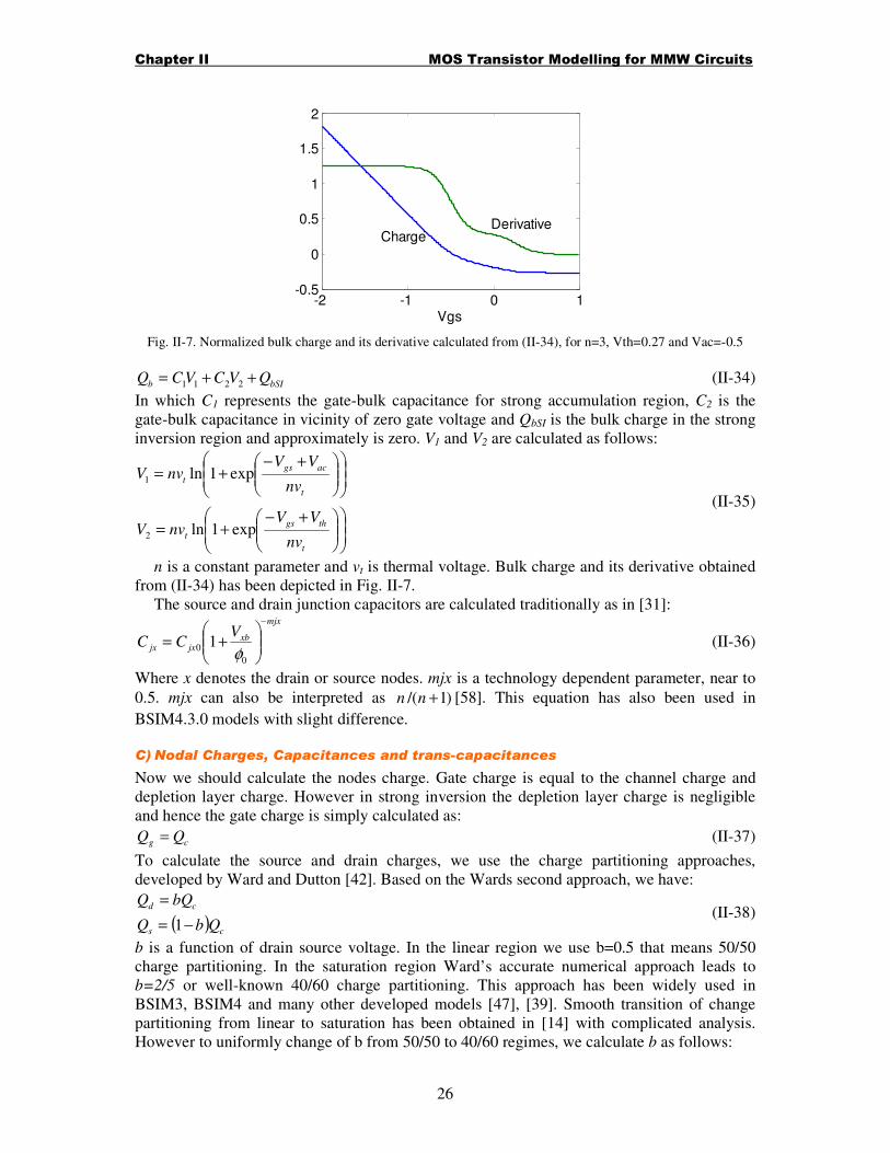
Fig. II-7. Normalized bulk charge and its derivative calculated from (II-34), for n=3, Vth=0.27 and Vac=-0.5
bSIb QVCVCQ ++= 2211 (II-34)
In which C1 represents the gate-bulk capacitance for strong accumulation region, C2 is the
gate-bulk capacitance in vicinity of zero gate voltage and QbSI is the bulk charge in the strong
inversion region and approximately is zero. V1 and V2 are calculated as follows:
+−+=
+−+=
t
thgs
t
t
acgs
t
nv
VVnvV
nv
VVnvV
exp1ln
exp1ln
2
1
(II-35)
n is a constant parameter and vt is thermal voltage. Bulk charge and its derivative obtained
from (II-34) has been depicted in Fig. II-7.
The source and drain junction capacitors are calculated traditionally as in [31]: mjx
xbjxjx
VCC
−
+=
0
0 1φ
(II-36)
Where x denotes the drain or source nodes. mjx is a technology dependent parameter, near to
0.5. mjx can also be interpreted as )1/( +nn [58]. This equation has also been used in
BSIM4.3.0 models with slight difference.
C) Nodal Charges, Capacitances and trans-capacitances
Now we should calculate the nodes charge. Gate charge is equal to the channel charge and
depletion layer charge. However in strong inversion the depletion layer charge is negligible
and hence the gate charge is simply calculated as:
cg QQ = (II-37)
To calculate the source and drain charges, we use the charge partitioning approaches,
developed by Ward and Dutton [42]. Based on the Wards second approach, we have:
( ) cs
cd
QbQ
bQQ
−=
=
1 (II-38)
b is a function of drain source voltage. In the linear region we use b=0.5 that means 50/50
charge partitioning. In the saturation region Ward’s accurate numerical approach leads to
b=2/5 or well-known 40/60 charge partitioning. This approach has been widely used in
BSIM3, BSIM4 and many other developed models [47], [39]. Smooth transition of change
partitioning from linear to saturation has been obtained in [14] with complicated analysis.
However to uniformly change of b from 50/50 to 40/60 regimes, we calculate b as follows:

Chapter II MOS Transistor Modelling for MMW Circuits
27
0 0.2 0.4 0.6 0.8 10.8
1
1.2
1.4
1.6x 10
-14
Vd
Cgd-Model
Cgd-Des. Kit
0 0.2 0.4 0.6 0.8 10
1
2
3
4x 10
-14
Vg
Cgg-Model
Cgg-Des. Kit
Fig. II-8. Cgd and Cgg of the transistor capacitances, calculated form our model, in comparison with the foundry
design kit data
′−=
cp
ds
V
Vb tanh
10
1
2
1 (II-39)
Vcp is a constant voltage that controls the transition slope.
Having the gate, source and drain charges one can simply calculate the small signal
capacitance and trans-capacitances as follows:
j
iij
V
QC
∂
∂= (II-40)
In which i and j stand for gate, source and drain nodes. Different capacitances have been
calculated in Appendix A. Here to evaluate our model, some of the calculated capacitances
have been shown in Fig. II-8, in comparison with the foundry design kit data.
II.2.3 Small Signal Model
The commonly used small signal model for intrinsic MOS transistor for RF applications has
been shown in Fig. II-9 [59], [60]. In this model Rg represents the small resistance due to the
distributed resistance of gate interconnects. Rg will be discussed in detail in next sections and
we will propose our new model for it. Rgs accounts for non-quasi-static nature of the channel
and will be discussed in this section. Capacitances in the model were calculated in the
previous section. gm and gds is calculated in this section using our I-V model in the previous
section. Please note that this model is only for transistor core and is too simple to be used as a
complete small signal model in MMW frequencies. In future we will describe our small signal
and Y parameter model for a complete transistor.
Before small signal analysis, the transistor’s bias condition should be calculated with DC
analysis, using the large signal model of transistor. Then the bias condition is used for
Fig. II-9. Commonly used small signal model for MOS transistor core
Chapter II MOS Transistor Modelling for MMW Circuits
28
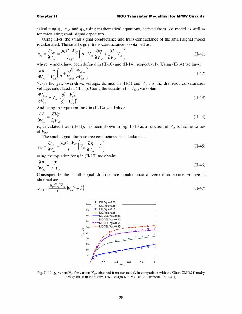
calculating gm, gmb and gds using mathematical equations, derived from I-V model as well as
for calculating small signal capacitors.
Using (II-8) the small signal conductance and trans-conductance of the small signal model
is calculated. The small signal trans-conductance is obtained as:
∂
∂+
∂
∂+=
∂
∂= ds
odod
od
eff
effox
gs
dsm V
VVV
L
WC
V
Ig
ληη
µ0 (II-41)
where η and λ have been defined in (II-10) and (II-14), respectively. Using (II-14) we have:
∂
∂+=
∂
∂
od
dsat
dsatodod V
V
VVV3
2
2
1 ηηη (II-42)
Vod is the gate over-drive voltage, defined in (II-3) and Vdsat is the drain-source saturation
voltage, calculated in (II-11). Using the equation for Vdsat we obtain:
( )222
0
22
00
od
odth
od
dsat
V
VV
V
V
+
−=
∂
∂
φ
φ (II-43)
And using the equation for λ in (II-14) we deduce:
32
0
2
0
3
odod V
V
V λ
λλ=
∂
∂ (II-44)
gm calculated from (II-41), has been shown in Fig. II-10 as a function of Vds for some values
of Vgs.
The small signal drain-source conductance is calculated as:
+
∂
∂=
∂
∂= λ
ηµ
ds
od
effox
ds
dsds
VV
L
WC
V
Ig
0 (II-45)
using the equation for η in (II-10) we obtain:
3
3
dsodds VVV
ηη=
∂
∂ (II-46)
Consequently the small signal drain-source conductance at zero drain-source voltage is
obtained as:
( )λµ
+= 2/30
0 od
effox
ds VL
WCg (II-47)
0 0.2 0.4 0.6 0.8 1
5
10
15
20
25
30
35
40
45
50
Vds
Gm
(mS
)
DK, Vgs=0.35
DK, Vgs=0.45
DK, Vgs=0.55
DK, Vgs=0.65
MODEL,Vgs=0.35
MODEL,Vgs=0.45
MODEL,Vgs=0.55
MODEL,Vgs=0.65
Fig. II-10. gm versus Vds for various Vgs, obtained from our model, in comparison with the 90nm CMOS foundry
design kit. (On the figure, DK: Design Kit, MODEL: Our model in II-41))

Chapter II MOS Transistor Modelling for MMW Circuits
29
0 0.2 0.4 0.6 0.8 10
10
20
30
40
50
60
Vds
Gds(m
S)
DK, Vgs=0.35
DK, Vgs=0.45
DK, Vgs=0.55
DK, Vgs=0.65
DK, Vgs=0.75
MODEL,Vgs=0.35
MODEL,Vgs=0.55
MODEL,Vgs=0.65
MODEL,Vgs=0.75
0.5 10
2
4
6
0 0.2 0.4 0.6 0.8 10
1
2
3
4
5
Vds
Gm
b(m
S)
DK, Vgs=0.35
DK, Vgs=0.45
DK, Vgs=0.55
MODEL,Vgs=0.35
MODEL,Vgs=0.45
MODEL,Vgs=0.55
(a) (b)
Fig. II-11. gds (a) and gmb versus Vds for various Vgs, obtained from our model, in comparison with the 90nm
CMOS foundry design kit. (On the figure, DK: Design Kit, MODEL: Our model in II-41))
And finally the small signal source-bulk trans-conductance is calculated as:
bs
thm
bs
dsmb
V
Vg
V
Ig
∂
∂−=
∂
∂= (II-48)
Using the threshold voltage equation in (II-9) we obtain:
( )sbmmb Vgg 21 2γγ +−= (II-49)
Vsb is the source-bulk voltage, γ1 and γ2 are constant body effect parameters, defined in (II-
9). gds and gmb, calculated from (II-45) and (II-49), has been shown in Fig. II-11 as a function
of Vds for some values of Vgs.
II.2.3.1 Non-Quasi-Static Effect
NQS effect is considered as a consequence of the required transport time of the charges along
the channel length, from source to drain [38]. As we mentioned earlier, many complicated
models have been proposed to deal with NQS effect. However most of practical transistor
models use approximated approaches for this effect. In [61] and [40] analytic equations have
been developed to express the NQS effects on small signal model. Based on this analysis, the
small signal trans-conductance and gate capacitance is scaled as:
mbmnqsmb
mmnqsm
gg
gg
ζ
ζ
=
=
_
_ (II-50)
mζ is NQS scaling function, defined as:
( )ν
νζ
sinh=m (II-51)
In which:
( ) nqsj ωτν 31+= (II-52)
nqsτ is the NQS time constant and in the strong inversion region is calculated as:
( )sthgeff
eff
nqsnVVV
nL
−−=
0
2
µτ (II-53)
Where n is a constant parameter. For gate capacitance, the NQS scaling function has been
obtained as:
( )( )νν
νζ
sinh
1cosh −=c (II-54)

Chapter II MOS Transistor Modelling for MMW Circuits
30
Assuming 1<nqsωτ the first approximation of (II-51) and (II-54) is obtained as:
21
1
1
1
nqsc
nqs
m
j
j
ωτζ
ωτζ
+
=
+=
(II-55)
These first order approximations can be introduced in the transistor small signal model,
simply by adding a resistance in series with gate-source capacitance, as in Fig. II-9. Doing
this, from Fig. II-9 we have:
gs
nqsgs
nqsgs
m
nqsgs
nqsm
CRCj
C
gRCj
g
ω
ω
+=
+=
1
1
1
1
_
_
(II-56)
This approximation has been used in BSIM3v3 and BSIM4.3.0 models, as well as in other
models [60], [38]. Rnqs in BSIM3v3 and BSIM4.3.0 has been noted as RElmore and Rii
(Intrinsic Input Resistance), respectively and is calculated as:
cheff
eff
nqsQ
LR
εµ
2
= (II-57)
Where ε is the Elmore constant, theoretically equal to 5, µeff is the effective mobility and Qch
is the equivalent channel charge, calculated in (II-13) and (II-33), respectively. In our case
Leff is (L-x), x calculated in (II-32). It must be noted that (II-57) and (II-53) have the same
origin. This can be shown simply by substituting Qch with Cgs(Vgs-Vth), as in [4] and defining
τnqs as RnqsCgs. Equation (II-57) shows the quadratic decrease of NQS effect with decreasing
channel length. So in practical measurement of NQS effects, transistors with very large gate
length are fabricated, e.g. 300um in 0.5 um technology [60], so that the NQS effect is evident.
To give a sense about the NQS static effects in the technology used in our work, i.e. 90nm
CMOS, We have calculated ζm from (II-55), using the foundry DRM data. Fig. II-12 shows
the amplitude and phase of ζm, with respect to frequency. This figure shows that at our design
frequency, i.e. 30 GHz, NQS effects are not negligible.
108
109
1010
1011
0.9
0.95
1
1.05
Frequency (Hz)
Ma
gn
itu
de
ζ
108
109
1010
1011
-60
-50
-40
-30
-20
-10
0
Frequency (Hz)
Ph
ase
ζ (
de
gre
e)
Fig. II-12. Magnitude and phase of ζm, calculated using (II-55) and for 90nm CMOS technology
Chapter II MOS Transistor Modelling for MMW Circuits
31
II.2.4 Noise Model
As CMOS technology expands into the RF band, high frequency noise performance of MOS
transistor becomes more important and having a good noise model is an essential need. In this
context, first modeling was proposed by Van Der Ziel in 1963 in suggestion of noise in FET
transistors [62]. Then V.Z. model was proven and accepted as a successful noise model for
old CMOS technologies [63], [64], [65], [66]. Based on V. Ziel noise model, the main noise
contribution is due to the channel thermal noise, modeled as a current source between drain
and source and calculated as:
0
2
4 dnd gkTf
i⋅=
∆γ (II-58)
In which k is the Boltzmann’s constant, T is the ambient temperature. γ is a function of
device parameters and bias and its value is between 2/3 for saturation region and 1 for Vds=0.
gd0 is the channel conductance in zero drain-source voltage
The other noise mechanism in V. Ziel model is the induced gate noise, modeled as a shunt
current source parallel, calculated as:
g
nggkT
f
i⋅=
∆δ4
2
(II-59)
δ is a bias-dependent parameter and gg is the noise equivalent conductance in the gate node.
However in short channel MOS transistors this model underestimates the noise
performance and hence in many works higher values of γ have been addressed [65], [67],
[68], [69]. Chen et al. developed a scenario for measurement and extraction of MOS transistor
noise parameters, specially the gate induced noise and compared the results with V. Ziel
model. They addressed noticeable discrepancy of the V. Ziel model with the measurement
results [70].
In recent years many researches have been focused on the noise modeling in MOS
transistors. Unfortunately the obtained results are not consistent with each other. The common
note accepted by all reports is that the main noise contribution is due to the channel thermal
noise, as claimed by V. Ziel [71], [72]. Also it was accepted that the gate induced noise is not
important for frequencies below much lower than the transistor cutoff frequency, fT (fT/f > 10)
[72], [73]. Many complicated models have been derived from physical analysis of the channel
charge and current. Some of these models express the excess noise (in comparison with V.
Ziel model) is due to the velocity saturation and hot electron effects in deep submicron
devices [74], [75]. In contrast, some other works declaimed this theory and presented different
ideas. Scholten et al. found that the experimental data can be explained with considering the
noise only in the Gradual Channel Region (GCR) (see Fig. II-13) and hence it not necessary
to deal with the high-filed effects at high Vds [76]. Goo et al. presented a simulation based
technique and showed that the main noise contribution comes from GCR and hence has the
ohmic nature [77]. Some other works considered both of GCR and VS (velocity saturation)
region, as well as channel length modulation [77]. In [71] a physical based compact noise
model was developed with treating the channel as a serious of infinitesimal resistors. Chen et
al. In [78] claimed that the excess noise is due to CLM, not the velocity saturation, because
electrons in VS region has not the ability of random moving.
Induced gate noise has not been considered in BSIM models, prior to BSIM4. The noise
model used in BSIM4 is based on the model in [77]. BISM4 noise model was studied in [79]
and it is shown that this model may leads to erroneous results, in the case of induced gate
noise. In [80] has been shown experimentally that BSIM4 noise model is not accurate in for
90nm CMOS technology, in 1.0GHz to 18GHz, but good agreement was achieved after

Chapter II MOS Transistor Modelling for MMW Circuits
32
adding a frequency-dependent noise source in the gate, as in V. Ziel model. PSP model uses
the improved Klassman Prins equation in modeling the channel thermal noise. This model has
specially developed for sub-0.1um technologies and has been accepted by CMC2 as standard
MOS transistor model [81]. PSP noise model comprises the induced gate noise and velocity
saturation effects. Experimental results in [82] show significant increase of the noise with
increasing the drain voltage, in the case of 70nm CMOS technology. The authors explained
that this is due to the CLM and increasing the short channel effect. Other noise sources such
as the shot-noise due to the impact ionization have been considered in noise modeling [72].
In contrast to the complicate models, presented in recent years, V. Ziel model, although
underestimates the noise parameters, but have very good prediction of the noise behavior of
sub-0.1um technologies [71]. This can be deduced from the measurement results in [70] for
0.18um technology, in [80] for 90nm technology and in [82] for 70nm technology. The
measurement results in [70] shows that the frequency-dependent behavior of the channel
thermal noise, the induced gate noise and their correlation coefficient is very near to that of V.
Ziel model. The measurement results in [80] shows that adding V. Ziel idea to the BSIM4
model leads to an accurate noise model. The results in [82] reveal significant discrepancy
between V. Ziel model and the measured data, however they have used fixed value for γ in
V. Ziel model and instead have corrected the error with an extra voltage-dependent resistor.
This is exactly equal to defining γ as a function of drain-source bias voltage. Using proper
bias-dependent value for γ , very good agreement with the experimental results has been
obtained, in the case of 0.18um technology [83].
Beside this, due to its simplicity, V. Ziel model has been widely used in getting insight to
the noise behavior of different circuits via mathematical analysis [40], [84], [85].
Consequently we have used V. Ziel model, with defining proper equations to express the
bias dependency of noise parameters to capture short channel effects, and using our I-V model
to calculate the channel conductance. In summary the noise model is as follows:
The drain current noise is calculated as:
0
2
4 dnd gkTf
i⋅=
∆γ (II-60)
Where gd0 is the drain-source conductance at zero Vds and is calculated from (II-47). γ is
bias dependent noise parameter. The original bias dependency of γ has been derived by V.
Ziel for long channel devices and has been used in [83] for 0.18um technology. However
based on the measurement results in [70] we have defined an empirical function as below:
Fig. II-13. Dividing the saturated channel to Gradual Channel Region (GCR) and Velocity Saturation region
(VSR) [72].
2 Compact Model Concile

Chapter II MOS Transistor Modelling for MMW Circuits
33
dsat
dsatds
V
VV22 +
= κγ (II-61)
where κ is a constant parameter and Vdsat is the saturation voltage, calculated in (II-27). Based
on this representation the channel noise increases linearly with Vds for Vds >>Vdsat and this
corresponds to the measurement results in [82] for 70nm technology. Finally the induced gate
noise is calculated as:
3/44
2
=⋅=∆
δδ g
nggkT
f
i (II-62)
in which:
0
22
5 d
gs
gg
Cg
ω= (II-63)
Drain noise and induced gate noises have physically same origin and hence are correlated. As
calculated by V. Ziel in the case of long channel device, and proven with measurement results
in [70] for short channel devices, the correlation coefficient is pure imaginary and frequency
independent:
395.0
22
*
j
II
IIc
ndng
ndng
=
=
(II-64)
II.3 Distributed Analysis When the frequency increases up to a certain limit, distributed model of transistor should be
considered. The limit of frequency depends on the length of different conducting objects in
the MOS transistor structure, in comparison with the wavelength in that object. It is
emphasized that different objects of the MOS structure have different wave propagation
characteristics and hence the related wavelength in different.
The most susceptible part of a MOS transistor to the distributed effects is its gate, due to
high resistance and high capacitance. Channel resistance and gate capacitance causes a delay
on propagating the charges along the gate length. This is the well known non-quasi static
effect that has been modeled in earlier studies as a distributed RC network [86], [87]. On the
other hand high resistance of the gate finger, coupled with the high gate capacitance reveals
slow wave along the gate width and hence the distributed modeling should be used to
accurately calculate the gate admittance, as well as the transistor trans-conductance and noise
performance, leading to the distributed transistor model.
Distributed nature of a MOS transistor has been considered in many works. In [88] the
effect of gate resistance noise was analyzed, considering RC distribution along the gate width.
In this work a ladder network obtained by treating the single transistor as a cascade of some
small transistors via gate resistances. Razavi et al. investigated the effect of distributed gate
resistance on fT and fmax of MOS transistor [59]. They used the same approach, as in the
previous work and showed that the effective gate resistance is about 1/3 of the actual gate
finger resistance. In [89] transmission-line treatment and analysis has been used in
development of a high frequency small signal and noise model. In our knowledge this model
is the most accurate distributed model for MOS transistors. However this model is useful for a
single finger transistor and is not sufficient for modeling of multi-finger transistors. On the
other hand we will show that such complicated model is not necessary for a very small single
finger transistor.
Chapter II MOS Transistor Modelling for MMW Circuits
34
In this section we analyze and discus the distributed effect in the gate resistance, aiming to
find:
� Maximum frequency up to which, conventional lumped model can be used.
� Beyond this frequency, can the lumped model be corrected to capture the distributed
effects?
We will show that for optimum gate fingers in sub-0.1um technologies, conventional
lumped element model can be used beyond the possible frequencies for MOS transistors. In
addition, for some special applications the lumped element model can be used with modified
element values, obtained from our analysis.
II.3.1 Distributed Model
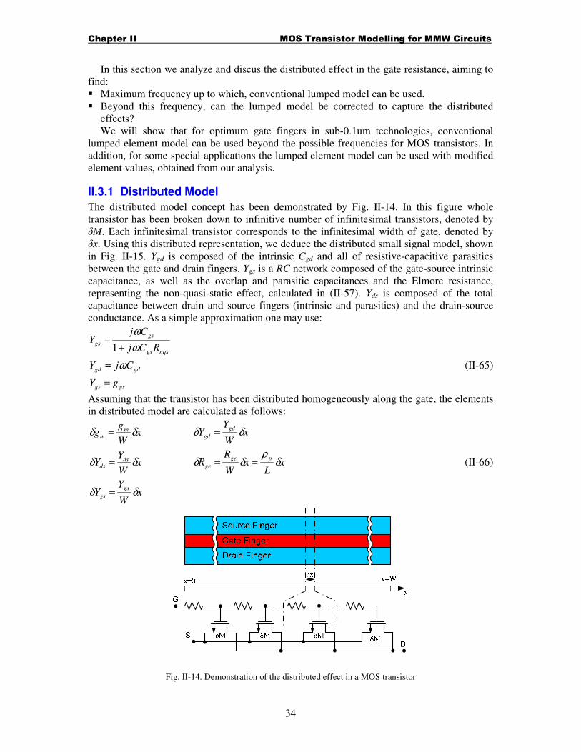
The distributed model concept has been demonstrated by Fig. II-14. In this figure whole
transistor has been broken down to infinitive number of infinitesimal transistors, denoted by
δM. Each infinitesimal transistor corresponds to the infinitesimal width of gate, denoted by
δx. Using this distributed representation, we deduce the distributed small signal model, shown
in Fig. II-15. Ygd is composed of the intrinsic Cgd and all of resistive-capacitive parasitics
between the gate and drain fingers. Ygs is a RC network composed of the gate-source intrinsic
capacitance, as well as the overlap and parasitic capacitances and the Elmore resistance,
representing the non-quasi-static effect, calculated in (II-57). Yds is composed of the total
capacitance between drain and source fingers (intrinsic and parasitics) and the drain-source
conductance. As a simple approximation one may use:
gsgs
gdgd
nqsgs
gs
gs
gY
CjY
RCj
CjY
=
=
+=
ω
ω
ω
1
(II-65)
Assuming that the transistor has been distributed homogeneously along the gate, the elements
in distributed model are calculated as follows:
xW
YY
xL
xW
RRx
W
YY
xW
YYx
W
gg
gs
gs
pge
geds
ds
gd
gdm
m
δδ
δρ
δδδδ
δδδδ
=
===
==
(II-66)
Fig. II-14. Demonstration of the distributed effect in a MOS transistor

Chapter II MOS Transistor Modelling for MMW Circuits
35
Fig. II-15. Equivalent small signal representation for distributed model of MOS transistor
Rge is the gate electrode resistance, calculated as:
L
WR
p
ge
ρ= (II-67)
where W is the gate width, L is the gate length and ρp is the gate poly silicon sheet resistance.
Note that Rge is different from Rg that is used in the small signal lumped model, as will be
described later.
The circuit of Fig. II-15 is described by a second order differential equation (See Appendix
B). Solving this equation we obtain the voltage and current along the gate as:
( ) ( )sgsdgd
pxxVYVY
WLeVeVxV +++= −−+
2
..
κ
ρκκ (II-68)
( ) ( )xx
p
eVeVL
xI .. κκ
ρ
κ −−+ −=
In which:
( )gsgd
pYY
WL+=
ρκ (II-69)
ρp is the gate poly silicon sheet resistance. V+ and V- are found from the boundary conditions
for the differential equation. To find the boundary conditions, we consider two possible ways
of gate finger connection, i.e. connection to single end of the gate finger (single connection),
or connection to the both ends (double connection). For single connection gate finger the
required boundary conditions are:
( )
( ) 0
0
=
=
=
=
Wx
gx
xI
VxV (II-70)
And the required boundary conditions for double connection case are:
gWx
gx
VV
VV
=
=
=
=0 (II-71)
Using these boundary conditions one can solve (II-68) to obtain V(x) and then the currents
into the transistor nodes are calculated. Consequently Y parameters are calculated.
For single connection gate Y parameters are as follows (See Appendix B for details):

Chapter II MOS Transistor Modelling for MMW Circuits
36
( ) ( )W
WYYY gsgd
κ
κtanh11 +=
( ) ( )W
WYgY gdm
κ
κtanh21 −= (II-72)
( ) ( )W
WgYY mgs
κ
κtanh31 +−=
( )W
WYY gd
κ
κtanh12 −=
( ) ( ) ( )dsgdgdm
gsgd
gdYY
W
WYg
YY
YY ++
−−
+=
κ
κtanh122
( ) ( )dsgsm
gsgd
gdY
W
WYg
YY
YY −
−+
+−=
κ
κtanh132
( )gsgs Y
W
WYY −
−=
κ
κtanh113
( ) ( )mds
gsgd
gdm
gs gYW
W
YY
YgYY +−
−
+
−=
κ
κtanh123
( ) ( )mdsgs
gsgd
gsm
gs gYYW
W
YY
YgYY +++
−
+
+−=
κ
κtanh133
The equations for Y11, Y12, Y21 and Y22 are similar to that of [89].
For double connection gate Y parameters are as follows (See Appendix B for details):
( ) ( )( )
−+=
WW
WYYY gsgd
κκ
κ
sinh
1cosh211
( ) ( )( )
−−=
WW
WYgY gdm
κκ
κ
sinh
1cosh221 (II-73)
( ) ( )( )
−+−=
WW
WgYY mgs
κκ
κ
sinh
1cosh231
( )( )
−
−−−= 1
sinh
1cosh212
WW
WYYY gdgd
κκ
κ
( )( )
( )dsgd
gsgd
gdm
gd YYWW
W
YY
YgYY ++
−
−
+
−−= 1
sinh
1cosh222
κκ
κ
( )( ) ds
gsgd
gsm
gd YWW
W
YY
YgYY −
−
−
+
+= 1
sinh
1cosh232
κκ
κ
( )( ) gsgs Y
WW
WYY −
−
−−= 1
sinh
1cosh213
κκ
κ
( )( )
( )mds
gsgd
gdm
gs gYWW
W
YY
YgYY +−
−
−
+
−−= 1
sinh
1cosh223
κκ
κ

Chapter II MOS Transistor Modelling for MMW Circuits
37
( )( )
( )mdsgs
gsgd
gsm
gs gYYWW
W
YY
YgYY +++
−
−
+
+= 1
sinh
1cosh233
κκ
κ
To validate the accuracy of results, we have simulated the distributed model of Fig. II-15
in ADS, using the foundry design kit data for 90nm CMOS technology. A single transistor
with W=15um has broken to 100 sections, as in Fig. II-15. The resulted Y parameters have
been compared with the Y parameters obtained from our analysis and that of the lumped
model, described in the next section. Y11, Y12 and Y21 have been shown in Fig. II-16 and Fig.
II-17 shows Y13, Y23 and Y33.
II.3.2 Comparison With Lumped Model
The lumped small signal counterpart of the distributed model in Fig. II-15 has been shown in
Fig. II-18. In this figure Rg is the effective gate resistance, calculated as [90]:
LN
WR
f
fp
g3
ρα= (II-74)
0 20 40 60 80 1000
0.5
1
1.5
2
Ima
g P
art
of Y
11
(m
S)
0 20 40 60 80 1000
0.5
1
1.5
2
Re
al P
art
of Y
11 (
mS
)
0 20 40 60 80 100-0.5
-0.4
-0.3
-0.2
-0.1
0
Frequency (GHz)
Ima
g P
art
of Y
12
(m
S)
0 20 40 60 80 100-0.5
-0.4
-0.3
-0.2
-0.1
0
Frequency (GHz)
Rea
l P
art
of Y
12
(m
S)
0 20 40 60 80 100-10
-8
-6
-4
-2
0
Ima
g P
art
of Y
21
(m
S)
0 20 40 60 80 1000
5
10
15
20
Rea
l P
art
of Y
21
(m
S)
Lumped Model
ADS Simulation
Distributed Model
Lumped Model
ADS Simulation
Distributed Model
Lumped Model
ADS Simulation
Distributed Model
Lumped Model
ADS Simulation
Distributed Model
Lumped Model
ADS Simulation
Distributed Model
Lumped Model
ADS Simulation
Distributed Model
Fig. II-16. Y11, Y12 and Y21 obtained from lumped model and distributed model, in comparison with the
simulation in ADS for 90nm CMOS technology

Chapter II MOS Transistor Modelling for MMW Circuits
38
0 20 40 60 80 100-1.5
-1
-0.5
0
Re
al P
art
of Y
13
(m
S)
0 20 40 60 80 100-1.5
-1
-0.5
0
Ima
g P
art
of Y
13
(m
S)
0 20 40 60 80 100-20
-15
-10
-5
Rea
l P
art
of Y
23
(m
S)
0 20 40 60 80 1000
2
4
6
Ima
g P
art
of Y
23
(m
S)
0 20 40 60 80 1005
10
15
20
Frequency (GHz)
Re
al P
art
of Y
33
(m
S)
0 20 40 60 80 100-6
-4
-2
0
2
Frequency (GHz)
Ima
g P
art
of Y
33
(m
S)
Lumped Model
Distributed Model
ADS Simulation
Lumped Model
Distributed Model
ADS Simulation
Lumped Model
Distributed Model
ADS Simulation
Lumped Model
Distributed Model
ADS Simulation
Lumped Model
Distributed Model
ADS Simulation
Lumped Model
Distributed Model
ADS Simulation
Fig. II-17. Y13, Y23 and Y33 obtained from lumped model and distributed model, in comparison with the
simulation in ADS for 90nm CMOS technology
Fig. II-18. The lumped small signal model, counterpart of the distributed model in Fig. II-15
In which ρp is the gate poly-silicon sheet resistance, Wf and L are the gate finger width and
length, respectively, Nf is the number of fingers. α is a coefficient equal to 1 for single
connection gate finger and 4 for double connection. This equation has been used in many
reported works and in BSIM4.3.0 model with small modifications [40], [91]. Divide by 3 in
(II-74) is due the distributed effect of the gate finger resistance, in conjunction with gate
capacitance, in low frequencies. This has been derived in Appendix C.
To compare the distributed model of Fig. II-15 with its lumped counterpart in Fig. II-18, we
have defined an error measure, named Distributive Effect Error (DEE) as:

Chapter II MOS Transistor Modelling for MMW Circuits
39
∑∑= =
−×=
3
1
3
1
100i j
D
ij
D
ij
L
ij
ijY
ijYijYDEE (II-75)
Where L
ijY and D
ijY are Y-parameters of the lumped and distributed models, respectively. This
measure has been calculated for some values of gate width, in our 90nm CMOS technology,
and has been depicted in Fig. II-19. This figure reveals two important notes:
� The distributive effect is reduced with double connecting the gate finger. For small values
of W, DEE for single connection with gate width of 2W is equal to that of double
connection with gate width of W. This is very important, since the designer can choose the
gate finger width for double connection case, twice of that of the single connection. These
halves the gate pad length (See the next section) and hence halves the pad parasitic
capacitance.
� For small widths of gate finger the distributive effect is negligible and hence the lumped
model can be used. For example, in Fig. II-19-b, for W=2um DEE is less than 0.02% at
30GHz. On the other hand, practically there is an optimum value of gate finger width that
minimizes the noise figure and the optimum Wf in 90nm technology is about 2um [92].
Consequently in our work distributed model is not required.
II.4 Layout Issues
In our knowledge even modern RF-CMOS design kits have been designed for the frequencies
well below the millimeter wave frequency band. So for the MMIC’s in such frequencies, the
designer should have the ability to develop own design tool, based on him or her knowledge
to integrate many high frequency effects together with the foundry design kit tools and data.
In the case of our work the problem is more sever, since the technology we have used, and the
related foundry design kit is digital process, it does not have any proposition for the high
frequency effects, as well as layout of MOS transistor for RF applications. So we should
design the transistor layout, as apart of our works.
The first issue in the MOS transistor layout is the gate structure. In contrast with digital
circuits, in which transistors are normally designed with the minimum size, in analog circuits
large W/L is required. Specially in RF applications large W/L is necessary to achieve the
required trans-conductance. A transistor with large W/L can not be laid out as simple gate,
due to performance reduction for long gate and some technological restrictions [40].
Consequently special layout issues must be considered. The most commonly used
configuration in the design of RF IC’s is the multi-finger layout [40], [92]. However other
gate structure, namely Waffle structure, has been presented and discussed [91], [93]. Two
types of Waffle (WF) structure, i.e. Manhattan Gate (MG) and Manhattan Interconnect (MI)
have been depicted in Fig. II-20. Two different implementation of Multi-Finger (MF) gate
structure have been shown in Fig. II-21. The detail of multi finger structures will be described
in the next section.
� Multi-finger structure offers low gate resistance and simple design and parasitic extraction.
The main problem of this structure is that increasing the number of fingers causes more
parasitic effects. The parasitic effect mainly arises from coupling between the gate pad (to
integrates the fingers outside the active area) and the substrate, as well as the drain-gate
and (or) source-gate overpasses [93], [92]. The main advantage of WF structure is its
compactness. In [93] better noise figure have been reported for this structure in below
10GHz, in comparison with MF structure. Nonetheless WF is not a known gate structure in
CMOS RF design. It may be useful in analog designs in which many transistors are used.
In our knowledge, the most important problem with this structure is its modeling issues

Chapter II MOS Transistor Modelling for MMW Circuits
40
100
101
102
10-10
10-5
100
105
Frequency (GHz)
Dis
trib
utiv
e E
ffe
ct E
rro
r (%
)
W=15um
W=10um
W=5um
W=1um
W=2um
100
101
102
10-10
10-5
100
105
Frequency (GHz)
Dis
trib
utiv
e E
ffe
ct E
rro
r (%
)
W=1umW=2um
W=5um
W=10um
W=15um
(a) (b)
Fig. II-19. Distributive effect error measure, defined in (II-75), for various values of gate width, W(a) for single
connection and (b) for double connection
and increased and complicated parasitic effects, specially in higher frequencies. Most of
available MOS transistor models like BSIM3 [23] and BSIM4 [24] uses Quasi-Two-
Dimensional (QTD) assumption, that is deviated in WF structure. Due to the following
reasons, we have chosen the multi-finger gate structure in our layout:
� The models available on the foundry design kit is for multi-finger gate structure
� Parasitic effects modeling is very complicate in WF gate structure
Accurate parasitic effects modeling is very important in our design
II.4.1 Proposed Layout
Four different approaches for laying out the MOS transistor with multi-finger gate structure,
has been depicted in Fig. II-22 to Fig. II-25. In Fig. II-22 and Fig. II-23 single connection gate
has been used and Fig. II-24 and Fig. II-25 single connection gate has been implemented.
For equal finger width, the single connection strategies leads to higher gate resistance , but
decreases the other parasitic effects, in comparison with the double connection gate structure.
For example, in the case of single connection gate, the capacitive coupling between the gate
pad and substrate is half of that of the double connection gate. Also the gate-drain parasitic
capacitance in single connection gate is lower than double connection structure, in
consequence of overpass of drain fingers in case of double connection. Consequently for the
applications in which the gate resistance is not so important, the single connection is
preferred. However the above discussion is true for equal finger number. If the designer aim
to achieve a certain value of gate resistance for a given value of transistor gate width, W, then
based on (II-74) finger width (Wf) of double connection structure will be 4 times of single
connection structure. So we have: sc
f
dc
f WW 4= (II-76)
Super-scribes dc and sc denote for double and single connection respectively. Also we have: dc
f
sc
f NN 4= (II-77)
Then the length of gate pad is calculated as:
dc
fit
dc
gpad
sc
fit
sc
gpad
NLL
NLL
2=
= (II-78)
And simply we deduce: dc
gpad
sc
gpad LL 2= (II-79)

Chapter II MOS Transistor Modelling for MMW Circuits
41
Sou
rse
(Metal1)
Sourse
(Metal1)
Sourse
(Metal1)
Drain
(Metal1)
Drain
(Metal1)
Sours
e
(Meta
l1)
Sours
e
(Meta
l1)
Sours
e
(Meta
l1)
Dra
in
(Meta
l1)
Dra
in
(Meta
l1)
Gate (P
oly)
(a) (b)
Fig. II-20. Manhattan Gate (a) and Manhattan Interconnect (b) implementation for MOS transistor layout.
(Reproduced from [91])
Sours
e
(Meta
l1)
Sours
e
(Meta
l1)
Dra
in
(Meta
l1)
Dra
in
(Meta
l1)
Active A
rea
Sours
e
(Meta
l1)
Sours
e
(Meta
l1)
Dra
in
(Meta
l1)
Dra
in
(Meta
l1)
Active A
rea
Fig. II-21. Single connection (a) and double connection (b) gate layout for MOS transistor
Guard
Rin
g (M
eta
l1)
Fig. II-22. Single connection multi finger gate structure, with guard ring close to the transistor core

Chapter II MOS Transistor Modelling for MMW Circuits
42
Fig. II-23. Single connection multi finger gate structure, with guard ring far from transistor core
Fig. II-24. Double connection multi finger gate structure, with guard ring close to the transistor core
Fig. II-25. Double connection multi finger gate structure, with guard ring from transistor core

Chapter II MOS Transistor Modelling for MMW Circuits
43
In addition, reduced number of gate fingers, reduces the drain/source overpasses and this also
reduces the parasitic capacitances. The other important note is distributive effects. As we
analyzed in the previous section, the distributed effects in double connection structure are
significantly lower than that of single connection structure. Consequently we have chosen the
double connection structure in our design.
The difference between Fig. II-24 and Fig. II-25 is in their guard ring. In Fig. II-24 the
substrate resistance is less than that of Fig. II-25, but the parasitic capacitance of source pad
with the guard ring is high, due to the source fingers overpass. So choosing the proper one
depends on the importance of these effects. This is exactly similar in the case of Fig. II-22, in
comparison with Fig. II-23. Accurate comparison of different layouts needs complicated
analysis and simulation. However we found that the layout of Fig. II-25 is better than Fig. II-
24 for LNA in our work.
II.5 Our Comprehensive Model Our model basis is treatment of each gate finger as a separate transistor, and then connecting
them to form the complete model of the multi finger transistor, considering all off the layout
dependent parameters. The layout of the complete transistor is also broken to the layout of
partial transistors. Hereafter we denote the partial transistors as ∆M. Most of the layout
dependent parameters are included in the partial transistor model, and some of them are
comprised in the multi finger model. Partial transistor model is derived from our I-V model,
capacitance model, noise model, small signal model, as well as physical layout issues. Each
partial transistor is composed of an intrinsic transistor, parasitic elements and substrate model.
The intrinsic part, itself is composed of the small signal model of Fig. II-9, beside some
parasitic capacitors.
To form the complete transistor, either in layout or in model, partial transistors are
cascaded via resistances, capturing the gate pad resistance. Finally the interconnections model
is added.
II.5.1 Partial Transistor Model
The layout of a partial transistor and related small signal and noise model has been shown in
Fig. II-26. This layout is one section of the final layout of Fig. II-25. To be able to model the
double-end connection effect, we divide this transistor into two similar parallel transistors and
denote each half transistor with ∆M/2. Note that physically this is not possible, because drain
and source pads are not symmetrical with respect to the vertival symmetry line in Fig. II-26,
however this is possible as a hypothetic model.
As we noted earlier, the partial transistor model is composed of three sections: one intrinsic
MOS transistor model, a set of parasitic elements related to the intrinsic transistor and a set of
extrinsic layout dependent parasitic elements. The intrinsic transistor small signal model is as
Fig. II-9, except for the gate resistance. Here we will analyze partial transistor to develop a
small signal and noise model and derive proper equations to calculate the model elements.
One important note is that the modeling is a trade between accuracy and complexity. Many
complicated model can give high accuracy, but it will be inefficient in simulation. Also the
extractability of model elements should be considered in developing model.

Chapter II MOS Transistor Modelling for MMW Circuits
44
Guard Ring
Guard Ring
Gate Pad
Gate Pad
Source Pad
Drain Pad
WGR
WSP
WGP
WGP
WDP
WGR
WF
LF
SGRS
SGS
SGD
SGRD
LPT
Fig. II-26. the layout of the partial transistor
II.5.1.1 Drain/source resistance
Source and drain resistances are composed of two sections: one is bias independent contact
and diffusion resistance (drain/source sheet resistance) and the other is bias dependent
Source/Drain Extension (SDE) resistance. In BSIM3 these resistors have been considered as a
part of I-V characteristics, but in BSIM4 have been modeled as external asymmetric
resistances for source and drain. Since the foundry design kit we have used is based on
BSIM3 model, we does not need incorporate drain/source resistances in our model. In this
case the drain/source resistance is a hidden resistance and is not seen in AC simulation [94].
However this reduces the accuracy, since some of the parasitic capacitive couplings to the
internal drain/source node does not see this resistance and some others see it.
Drain and source resistances have been depicted in Fig. II-27. As in this figure, the
drain/source resistance is composed of contact resistance, salicide resistance, and SDE
resistance. The contact resistance is dominated by the salicide-SDE contact. In [40] simple
equation have been proposed for these resistances.
Fig. II-27. source/drain resistance representation for a short channel MOS device [40]

Chapter II MOS Transistor Modelling for MMW Circuits
45
II.5.1.2 Parasitic capacitances
Parasitic capacitances are divided into two main categories: parasitic capacitors in intrinsic
part and parasitic capacitors in extrinsic section. In the intrinsic part, parasitic capacitors are
among the gate, source and drain fingers. In the extrinsic section parasitic capacitors are
between gate pad and source/drain pad, as well as guard ring.
Parasitic capacitances in the intrinsic part, as depicted in Fig. II-28 [51], are three types:
One is the capacitance between the top of gate finger and the upper section of sidewall of
source/drain finger and related contacts (Ctop in Fig. II-28). The other is the capacitance
between the gate finger sidewall and lower section of sidewall of source/drain finger (Cside in
Fig. II-28). The third capacitor is due to the field fringing from gate sidewall to the
source/drain surface (Cf in Fig. II-28).
Conformal mapping is a powerful method, conventionally used for calculation of
capacitances in coplanar and parallel plate and strips, assuming quasi static condition [95].
Basis of this method is transformation of a complicated curve, representing the cross section
of a physical structure, into a simple shape in other plane, so that the new shape can be simply
analyzed to calculate the capacitance. This method has been used in calculation of gate
fringing capacitance and interconnection models in integrated circuits, with different
transforming function [51], [96], [97]. Base on conformal mapping from elliptical coordinate
system to a linear coordinate system, in [51] a closed form equation has been derived to
calculate the gate fringing capacitance:
( )2
11
2
2201
M
sp
fM
MM
WKC
−−=
π
εβ (II-80)
In which β1 is a fitting parameter, W is the gate width, ε0 is the free space permittivity and Ksp
is the relative permittivity of the material between gate and source/drain. M is defined as:
ox
sp
t
LM = (II-81)
tox is the oxide thickness and Lsp has been shown in Fig. II-28. However the gate fringing
capacitance is comprised in BSIM3v3 and hence we does not need to incorporate it separately
in our model. In BSIM3v3 this capacitance is modeled as [23]:
+=
ox
polyoxf
t
tC 1ln
2
π
ε (II-82)
Ctop in Fig. II-28 has been calculated in [51] as:
Gate
poly
P-well
Ctop L/2
tox
tp
Lsp
Cside
Cf
Source Drain
Csdf1
Csdf2
Source/drain
finger
contact
Drain/source
finger
contact
Tm
Lsdf
Fig. II-28. Parasitic capacitances in intrinsic part of the partial transistor [51]

Chapter II MOS Transistor Modelling for MMW Circuits
46
+=
sp
topeff
topL
LKWC
21ln
2 02
π
εβ (II-83)
Where β2 is a fitting parameter, Weff is the effective length of the source/drain finger,
considering the space between contacts, and Ktop is the relative permittivity of the dielectric
material on top of the gate finger. Cside in Fig. II-28 is simply calculated as:
−=
sp
pox
speffsideL
ttKWC 03 εβ (II-84)
where β3 is a fitting parameter and tp is the poly thickness. The capacitance Csdf1 in Fig. II-28
is calculated using the analysis in [96]:
+=
sdf
sdftop
sdfS
LWKC 1ln
0
21π
εβ (II-85)
Ktop is the relative permittivity of the dielectric material on top of the source/drain finger, β2 is
as in (II-83) and Lsdf and Ssdf have been shown in Fig. II-28. Finally the capacitance Csdf2 in
Fig. II-28 is calculated as:
=
sdf
mtopsdf
S
TWKC 032 εβ (II-86)
Extrinsic parasitic capacitances have been demonstrated in Fig. II-29, that is vertical cross
section of the partial transistor structure in Fig. II-26. These capacitances are due to the
coupling between gate pad, source/drain pad and guard ring. We will use the closed form
equation presented in [96] , after small modification, to calculate the capacitances. Note that
all of the calculated capacitances are per-unit-length values.
The capacitance between top of the source/drain pad and top of the guard ring (Crsd1 in Fig.
II-29) is calculated as:
+=
prsd
avrsd
S
WKC 1ln01
11π
εγ (II-87)
γ1 is a fitting parameter, K1 is the dielectric constant of the dielectric above the pads, Sprsd is
the space between the guard ring and source/drain pad. Wav is the average width of the guard
ring and source/drain pad. The capacitance between top of the source/drain and gate pads
(Cgsd1 in Fig. II-29) is calculated as series of two capacitors, 1gdsC′ and 1gdsC ′′ that are calculated
as:
STI STIP+
P-well
guard
ringSource
/drain
Crsd1
Crsd2
Crsd3
Cgsd1
Cgsd2
Cgsd3
Crg
STISTI P+
Source
/drain
Wpr
Spgsd
gate
Tm
guard
ring
Wpsd
Wpg Sprsd
Hm
Tpol
Fig. II-29. Parasitic capacitances between gate, sorce/drain and guard ring pads (extrinsic part of the partial
transistor)

Chapter II MOS Transistor Modelling for MMW Circuits
47
mm
pg
eqrsd
pgsd
aveq
rsd
HT
WKC
S
WKC
+=′′
+=′
01
0
11 1ln
ε
π
εγ
(II-88)
Where Wav is the average width of the source/drain and gate pads, γ1 is as previous equation,
Keq is the effective dielectric constant of the dielectric material on top of gate pad. Wpg, Tm and
Hm have been shown in Fig. II-29. The capacitance between the sidewall of source/drain pad
and the top of gate pad (Cgsd2 in Fig. II-29) is calculated from [51] with small modification:
++=
pgsd
mpgeq
gsdS
TWKC
21ln
2 02
2π
εβ (II-89)
β2 is the same as (II-83),Keq is the same as (II-88), Wpg, Tm and Spgsd have been shown in Fig.
II-29.
Cgsd3 in Fig. II-29 is calculated using (II-89), replacing Keq, Wpg and Tm with K3, Wpsd and Tpoly
, respectively. K3 is the dielectric constant of the dielectric material above gate and under
source/drain pads. Wpsd and Tpoly have been shown in Fig. II-29. Crsd3 in Fig. II-29 is calculated
using (II-89), replacing Keq, Wpg, Tm and Spgsd with K3, Wpsd, Hm+Tpoly and Sprsd, respectively.
K3 is the dielectric constant of the dielectric material above gate and under source/drain pads.
Wpsd and Tpoly , Hm and Sprsd have been shown in Fig. II-29. Crg in Fig. II-29 is very small and
we neglect it and finally Crsd2 is calculated simply:
prsd
mrsd
S
TKC 022 ε= (II-90)
Considering all of the calculated capacitances, we have the equivalent circuit of Fig. II-30 for
the parasitic capacitances. In this figure gi, di and si are gate, drain and source nodes of
intrinsic transistor, respectively. Cxy_pe and Cxy_pi denote the total parasitic capacitance
between nodes x and y (x and y stands for gate, source, drain and guard ring), in the extrinsic
and intrinsic parts, respectively. The capacitors in this model are calculated based on our
previous calculations, as follows:
pegspegd
gsdgsdgsdpegs
CC
CCCC
__
321_
=
++= (II-91)
Fig. II-30. Equivalent circuit model for parasitic capacitances of the partial transistor
Chapter II MOS Transistor Modelling for MMW Circuits
49
STIusw
usw
STIuaw
uaw
T
T
ρσ
ρσ
1
1
=
=
(II-94)
uawρ and uswρ are sheet resistance of the under active and under STI p-well, respectively.
Lateral resistances in Fig. II-32 are calculated as:
PT
GRGRSuawb
PT
SPGSGPuswb
PT
f
uawb
L
WSR
L
WSWR
L
WR
2/
2
2
2
1
+=
++=
=
ρ
ρ
ρ
(II-95)
The capacitances in Fig. II-32 are calculated as:
Fig. II-31. Various substrate modeling techniques: single resistor [99] (a), three-resistor [40] (b) and five-resistor
[24] (c)
Guard
Rin
g
Guard
Rin
g
Gate
Pad
Gate
Pad
Sourc
e P
ad
Dra
in P
ad
WG
R
WS
P
WG
P
WG
P
WD
P
WG
R
WF
LF
SG
RS
SG
S
SG
D
SG
RD
LP
T
Fig. II-32. Substrate electrical model for the partial transistor in Fig. II-26

Chapter II MOS Transistor Modelling for MMW Circuits
50
STI
PTSPSTI
m
PTSPd
bdpbsp
STI
PTGPSTIbgp
T
LWKC
H
LWKC
CC
CCCC
T
LWKC
02
01
21
21
0
ε
ε
ε
=
=
+==
=
(II-95)
In which KSTI and Kd are the dielectric constants of STI layer and the dielectric above STI,
respectively. ε0 is the free space permittivity.
The substrate model in Fig. II-32 can be represented as a RC network, as shown in Fig. II-
33. This circuit is very complicated to be analyzed and increases four extra nodes to the
transistor small signal model in Fig. II-18. Consequently it is not suitable for our simple
design tool. To simply the circuit, meanwhile preserving the accuracy, we have assumed that
extrinsic gate, source and drain nodes, (b, g and d in Fig. II-33), have approximately equal
voltage with the intrinsic ones (bi, gi and di in Fig. II-33). Using this approximation we obtain
the equivalent substrate Y model, as in Fig. II-34. As this figure shows with the simplified
model, there is not any extra node in the transistor model circuit, in comparison with Fig. II-
18.
Fig. II-33. Proposed substrate network as a RC circuit, derived from Fig. II-32.
Fig. II-34. Simplified Y-parameter model for substrate model circuit of Fig. II-33

Chapter II MOS Transistor Modelling for MMW Circuits
51
The Y parameters for this figure is calculated as follows. For detail see Appendix D.
( )( )
( )( )
( )
( )( )
( )( ) bi
g
dbi
bbbbbi
bgbpbibbg
b
bdbp
sgdg
bi
sdbi
b
sbpdbp
bbbbbi
sbpbbibbs
b
bdbp
ds
bi
g
gbidbi
b
bdbp
gbp
bbbbbi
bgbpbibbg
gbigbpg
bi
g
dbi
bbbbbi
bgbpbibbg
b
bdbp
dbidbpsd
yggyy
yyyg
y
gyyy
yy
yy
ggyy
ygyg
y
gyy
yyy
gyy
ggyy
yyygyyy
yggyy
yyyg
y
gyyyyy
λ
λ
λ
λλ
λ
λ
λ
λλ
λ
λ
λ
λλ
λ
λ
λ
λλ
−−
+−=′=′
−−−
+−=′
−+
+−
−
+++=′
+−
+++=′=′
2221
221
2
2
22221
221
2
2
2
2
2221
221
2221
221
2
2
22
(II-96)
In which:
sbibbsbibbsbpbbs
dbibbdbibbdbpbbd
gbibbgbibbgbpbbg
bbbbibbbibbbi
yggyyyygg
yggyyyygg
yggyyyyyg
gygyggyyy
222121
222121
222121
1212221
−+=
−+=
−+=
−−=
λ
λ
λ
λ
(II-97)
And:
xy
xyR
g1
= (II-98)
II.5.1.4 Final model for partial transistor
Final model of the partial transistor in Fig 2-35, is obtained combining parasitic
capacitances and substrate network with the intrinsic transistor model of Fig. II-9. In addition,
noise model of the intrinsic part, as discussed in section II.2.4, is added and the equivalent
noise of substrate is considered. Substrate noise is considered as resistive thermal noise [72],
due to the real part of each equivalent Y parameter in Fig. II-34. Final model has been shown
in Fig. II-35. Note that this model has only four nodes, as the simple model of Fig. II-9. This
simplifies all of the analysis and calculations, without need for time-consuming matrix
inversions.
Fig. II-35. Final partial transistor model, composed of intrinsic part, parasitic capacitances, substrate network and
noise model

Chapter II MOS Transistor Modelling for MMW Circuits
52
II.5.2 Complete Transistor Model
In section II.3.2 we deduced that the distributed model is not necessary for the single-finger
partial transistor model. However distributed nature affect the total transistor (composed of
some partial transistors), for which the layout has been shown in Fig. II-25. To capture the
distributed effects in our complete transistor model, we have used the model in Fig. II-36, that
is cascade of partial transistors via small resistances, showing the poly-silicon gate pad
resistance. As we noted earlier in the case of double connection gate fingers, each partial
transistor (∆M) with gate width WPT, is assumed as a parallel of two transistors, (∆M/2) with
gate width WPT/2. Considering the symmetry of the layout of Fig. II-25 and related model in
Fig. II-36, we can use the circuit in Fig. II-37 to analyze our model. Then Y-parameters of the
transistor will be 4-times of that of Fig. II-37. Note that in the case of odd number of fingers,
the width of the last partial transistor in Fig. II-37 will be half of the others. The analysis of
this circuit leads to a simple difference equation:
∆−=
∆+=
++
+
RIVV
YVII
nnn
innnn
11
1 (II-99)
The required initial condition is:
gVV =0
Fig. II-36. Distributed model of the transistor, corresponding to the layout of Fig. II-25
Fig. II-37. Distributed model of the transistor, used in analysis of the Fig. II-36

Chapter II MOS Transistor Modelling for MMW Circuits
53
II.5.2.1 Interconnect model
Since all of the interconnects in our design are implemented as Coplanar Transmission Line
(CPTL), we have designed special connections to the transistor pads to best match the CPTL
to the transistor inputs. The simplified layout has been shown in Fig. II-38-a. This structure
adds some extra parasitic effects to the transistor final model in Fig. II-36. We have used an
LC circuit to model these effects. The equivalent circuit for transistor interconnects has been
shown in Fig. II-38-b. More details will be given in chapter IV.
Gate Interconnect Drain Interconnect
GRing Intercon
nect
GRing Intercon
nect
GRing Interconnect
GRing Interconnect
(a) (b)
Fig. II-38. Interconnects to the transistor pads (a) and related equivalent LC model as a π section (b)

Chapter II MOS Transistor Modelling for MMW Circuits
54
ReferencesReferencesReferencesReferences [1] Peizhen Yang, W. S. Lau, V. Ho, C. H. Loh, S. Y. Siah, L. Chan, “A comparison between the quasi-
ballistic transport model and the conventional velocity saturation model for sub-0.1-¿m MOS transistors,”
In Proceedings of the IEEE Conference on Electron Devices and Solid-State Circuits (EDSSC 2007), pp.
99-102, Dec. 2007.
[2] Su Ke-Wei, Chen Kuang-Hsin, Chung Tang-Xuan, Chen Hung-Wei, Cheng-Chuan, Chen Hou-Yu,
Chang Chang-Yun, Lee Di-Hong, Wen Cheng-Kuo, Sheu Yi-Ming, Yang Sheng Jier, Chiang Chung-Shi,
Huang Chien-Chao, Yang Fu-Liang, Chia Yu-Tai,“Modeling isolation-induced mechanical stress effect
on SOI MOS devices,” In Proceedings of the IEEE International SOI Conference, pp. 80-82, Oct. 2003.
[3] I. Pesic, N. Gunther, A. Mutlu, M. Rahman, “Modeling C-V characteristics of deep sub - 0.1 micron
mesoscale MOS devices,” In Proceedings of the IEEE International Semiconductor Device Research
Symposium, pp. 140-141, Dec. 2003.
[4] J. R. Hauser, “A new and improved physics-based model for MOS transistors,” IEEE Transactions on
Electron Devices, vol. 52, Issue 12, pp. 2640-2647, Dec. 2005.
[5] J. Alvarado, A. Cerdeira, V. Kilshytska, D. Flandre, “A modified EKV PDSOI MOSFETs model,” In
Proceedings of the IEEE International Conference on Microelectronics, pp. 459-462, May 2006.
[6] W. Liu, “MOSFET models for SPICE simulation, Including BSIM3v3 and BSIM4”. New York, Wiley,
2001.
[7] R. Van Langevelde, A. J. Scholten, R. J. Havens, L. F. Tiemeijer, D. B. M. Klaassen, “Advanced compact
MOS modelling,” In Proceeding of the 31st European Solid-State Device Research Conference, pp. 81-
88, Sept. 2001.
[8] Yu Zhiping, Tian Lilin, “Recent progress in MOS compact modelling,” In Proceeding of the IEEE
International Conference on Solid-State and Integrated Circuits Technology, vol. 2, pp. 916-919, Oct.
2004.
[9] W. Prodanov, M. Valle, “A fully-automatic CAD toolbox for a MOS drain current model and its
parameters extraction,” In Proceedings of the IEEE Research in Microelectronics and Electronics, pp.
209-212, June 2006.
[10] J. He, J. Xi, M. Chan, H. Wan, M. Dunga, B. Heydari, A. M. Niknejad, and C. Hu, “Charge-based core
and the model architecture of BSIM5,” In Proceedings of the IEEE International Symposium on Quality
of Electronic Design (ISQED 2005), pp. 96–101, March 2005.
[11] G. Gildenblat, H. Wang, T.-L. Chen, Y. Guad, and X. Cai, “SP: an advanced surface-potential-based
compact MOSFET model,” IEEE Journal of Solid-State Circuits, vol. 39, no. 9, pp. 1394–1406, Sep.
2004.
[12] R. vanLangevelde, A. J. Scholten, G. D. J. Smit, D. B. M. Klaassen, G. Gildenblat, X. Li, H.Wang, and
W. Wu. “PSP model,” Koninklijke Philips Electronics. Available [Online]:
http://www.semiconductors.philips.com/Philips_Models.
[13] A. M. Chopde, S. Khandelwal, R. A. Thakker, M. B. Patil, K. G. Anil, “Parameter extraction for Mos
Model 11 using particle swarm optimization,” In Proceedings of the IEEE International Workshop on
Physics of Semiconductor Devices (IWPSD 2007), pp. 253, 256, Dec. 2007.
[14] H. J. Park, P. K. Ko, C. Hu, “A charge sheet capacitance model of short channel MOSFETs for SPICE,”
IEEE Transactions on Computer-Aided Design of Integrated Circuits and Systems, vol. 10, issue 3, pp.
376-389, March 1991.
[15] Choi Gil-Bok, Hong Seung-Ho, Jung Sung-Woo, Kang Hee-Sung, Jeong Yoon-Ha, “RF capacitance
extraction utilizing a series resistance deembedding scheme for ultraleaky MOS devices,” IEEE Electron
Device Letters, vol. 29, issue 3, pp. 238-241, March 2008.
[16] G. P. Fang, D. C. Yeh, D. Zweidinger, L. A. Arledge, V. Gupta, “Fast, accurate MOS table model for
circuit simulation using an unstructured grid and preserving monotonicity,” In Proceedings of the Asia
and South Pacific Design Automation Conference (ASP-DAC2005), vol. 2, pp. 1102-1106, Jan. 2005.
[17] B. R. Chawla, H. K. Gummel, and P. Kozak, “MOTIS–An MOS timing simulator,” IEEE Transaction on
Circuits and Systems, vol. CAS-22, no. 12, pp. 901–910, Dec. 1975.
[18] T. Shima, T. Sugawara, S. Moriayama, and H. Yamada, “Three-dimensional table look-up MOSFET
model for precise circuit simulator,” IEEE Journal of Solid State Circuits, vol. SSC-17, no. 6, pp. 449–
454, Jun. 1982.
[19] W. M. Coughran, E. H. Grosse, and D. J. Rose, “CAzM: A circuit-analyzer with macromodeling,” IEEE
Transaction on Electron Devices, vol. 30, no. 9, pp. 1207–1213, Sep. 1983.
[20] D. E. Root, S. Fan, and J. Meyer, “Technology independent large signal non quasi-static FET models by
direct construction from automatically characterized device data,” In Proceedings of the 21st European
Microwave Conference, pp. 927–932, Sep. 1991.

Chapter II MOS Transistor Modelling for MMW Circuits
55
[21] V. Bourenkov, K. G. McCarthy, A. Mathewson, “MOS table models for circuit simulation, IEEE
Transactions on Computer-Aided Design of Integrated Circuits and Systems, vol. 24, issue 3, pp. 352-
362, March 2005.
[22] Philips Electronics , “MOS Model 11,”
Available [Online]: http://www.nxp.com/models/mos_models/model11/index.html
[23] Weidong Liu, Xiaodong Jin, J. Chen, M. Jeng, Z. Liu, Y. Cheng, K. Chen, M. Chan, K. Hui, J. Huang, R.
Tu, P. Ko, and Chenming Hu, “BSIM3v3.2 MOSFET model and users manual,” Available [Online]:
http://wwwdevice. eecs.berkeley.edu/~bsim3.
[24] Xuemei (Jane) Xi, Mohan Dunga, Jin He, Weidong Liu, Kanyu M. Cao, Xiaodong Jin, Jeff J. Ou,
Mansun Chan, Ali M. Niknejad, Chenming Hu, “BSIM4.3.0 MOSFET model - user’s manual,” Available
[Online]: http://wwwdevice. eecs.berkeley.edu/~bsim4.
[25] Zhenyu (Jerry) Qi, Mircea R. Stan, “Accurate back-of-the-envelope transistor model for deep sub-micron
MOS,” In Proceedings of the IEEE International Conference on Microelectronic Systems Education, (
MSE '07), pp. 75-76, June 2007.
[26] N. Ishihara, T. Shimizu, “A simple equation model for RF MOSFET,” In Proceedings of the IEEE
Topical Meeting on Silicon Monolithic Integrated Circuits in RF Systems, pp. 93-96, Jan. 2006.
[27] W. Shockley, “A unipolar field-effect transistor,” In Proceedings of the IRE, vol. 40, issue 11, pp. 1365-
1376, Nov. 1952.
[28] C. T. Sah, “Characteristics of the metal-oxide-semiconductor transistors,” IEEE Transactions on Electron
Devices, vol. 11, issue 7, pp. 324-345, Jul 1964.
[29] G. Brezeanu, A. Sevcenco, “A compact model of submicron channel MOS transistor trans-conductance
for analog circuit simulation,” In Proceedings of the IEEE International Symposium on Signals, Circuits
and Systems (ISSCS 2007). vol. 1, pp. 1-4, July 2007.
[30] P. R. Gray, P. J. Hurst, S. H. Lewis, R. G. Meyer, “Analysis and design of analog IC's,” Fourth Edition, J.
Whiley & Sons, 2001.
[31] D. Johns and K. Martin, “Analog integrated circuit design,” John Wiley & Sons, Inc. 1997.
[32] K. A. Bowman, B. L. Austin, J. C. Eble, Tang Xinghai, J. D. Meindl, “A physical alpha-power law
MOSFET model,” IEEE Journal of Solid-State Circuits, vol. 34, issue 10, pp. 1410-1414, Oct. 1999.
[33] B. L. Austin, K. A. Bowman, Tang Xinghai, J. D. Meindl, “A low power trans-regional MOSFET model
for complete power-delay analysis of CMOS giga-scale integration (GSI),” In Proceedings of the IEEE
International ASIC Conference, pp. 125-129, Sept. 1998.
[34] T. Sakurai, A. R. Newton, “Alpha-power law MOSFET model and its applications to CMOS inverter
delay and other formulas,” IEEE Journal of Solid-State Circuits, vol. 25, issue 2, pp. 584-594, April
1990.
[35] Im Hyunsik, M. Song, T. Hiramoto, T. Sakurai, “Physical insight into fractional power dependence of
saturation current on gate voltage in advanced short channel MOSFETs (alpha-power law model),” In
Proceedings of the IEEE International Symposium on Low Power Electronics and Design (ISLPED'02),
pp. 13-18, 2002.
[36] M.S. Lundstrom and Z. Ren, ”Essential physics of carrier transport in nano-scale MOSFETs,” IEEE
Transaction on Electron Devices, vol. 49, p.133, 2002.
[37] T. Sakurai, A. R. Newton, “ A simple MOSFET model for circuit analysis,” IEEE Transactions on
Electron Devices, vol. 38, issue 4, pp. 887-894, April 1991.
[38] Y. P. Tsividis, “Operation and modeling of the MOS transistor,” New York, Mc Graw-Hill, 1987.
[39] S. H. Jen, B. J. Sheu, Park Yoondong, “A unified sub micrometer MOS transistor charge/capacitance
model for mixed-signal IC's,” IEEE Journal of Solid-State Circuits, vol. 34, issue 1, pp. 103-106, Jan.
1999.
[40] C. Enz, “An MOS transistor model for RF IC design valid in all regions of operation,” IEEE Transactions
on Microwave Theory and Techniques, vol. 50, issue 1, pp. 342-359, Jan. 2002.
[41] J. E. Meyer, “MOS models and circuit simulation,” RCA Rep., vol. 32, pp. 42-63, Mar. 1971.
[42] D. E. Ward, R. W, Dutton, “A charge-oriented model for MOS transistor capacitances,” IEEE Journal of
Solid-State Circuits, vol 13, issue 5, pp. 703-708, Oct 1978.
[43] Yuhua Cheng, Min-Chie Jeng, Zhihong Liu, Jianhui Huang, Mansun Chan, Kai Chen, Ping Keung Ko,
and Chenming Hu, “A physical and scalable model in BSIM3v3 for analog/digital circuit simulation,”
IEEE Transactions on Electron Devices, vol. 44, no. 2, pp. 277-287, Feb. 1997.
[44] O. Gouveia-Filho da Costa, M. C. Schneider, C. Galup-Montoro, “Advanced compact model for the
charges and capacitances of short-channel MOS transistors,” In Proceedings of the IEEE Symposium on
Integrated Circuits and Systems Design, pp. 18-21, Oct. 1999.
[45] S. H. Jen, B. J. Sheu, A. Y. Park, “An efficient MOS transistor charge/capacitance model with
continuous expressions for VLSI,” In Proceedings of the IEEE International Symposium on Circuits and
Systems (ISCAS '98). vol. 6, pp. 413-416, June 1998.

Chapter II MOS Transistor Modelling for MMW Circuits
56
[46] Xie Bing, He Yandong, Xu Mingzhen, Tan Changhua, “An unified model to characterize the strong
inversion high-frequency capacitance in thin oxide MOS structures under Fowler-Nordheim tunneling
injection condition,” In Proceedings of the IEEE International Conference on Solid-State and Integrated
Circuit Technology, pp. 447-449, Oct. 1998.
[47] H. J. Park, P. K. Ko, C. Hu, “A charge conserving non-quasi-state (NQS) MOSFET model for SPICE
transient analysis,” IEEE Transactions on Computer-Aided Design of Integrated Circuits and Systems,
vol. 10, issue 5, pp. 629-642, May 1991.
[48] Ananda S. Roy, Juzer M. Vasi, and Mahesh B. Patil, “A new approach to model Non-Quasi-Static (NQS)
effects for MOSFETs—Part II: small-signal analysis,” IEEE Transactions on Electron Devices, vol. 50,
no. 12, pp. 2401-2407, Dec. 2003.
[49] A. S. Roy, J. Vasi, and M. B. Patil, “A new approach to model NQS effect for MOSFET—Part I: Large
signal analysis,” IEEE Transactions on Electron Devices, vol. 50, no. 12, pp. 2393–2400, Dec. 2003.
[50] F. Stem, “Self-consistent results for n-Type Si inversion layers,” The Physical Review B, vol. 5, no. 12,
pp. 4891- 4899, Jun. 1972.
[51] Nihar R. Mohapatra, Madhav P. Desai, Siva G. Narendra, and V. Ramgopal Rao, “Modeling of parasitic
capacitances in deep submicrometer conventional and high-K dielectric MOS transistors,” IEEE
Transactions on Electron Devices, vol. 50, no. 4, pp. 959-966? April 2003.
[52] Fei Li, Sivakumar Mudanai, Leonard Franklin Register, and Sanjay K. Banerjee, “A physically based
compact gate C-V model for ultra-thin (EOT 1 nm and below) gate dielectric MOS devices,” IEEE
Transactions on Electron Devices, vol. 52, no. 6, pp. 1158-1148 , June 2005.
[53] Md. Itrat Bin Shams, K M. Masum Habib, Rajib Mikail, Quazi Deen Mohd Khosru, A. N. M Zainuddin
and A. Haque, “An improved physically based compact c-v model for MOS devices with high-k gate
dielectrics,” In Proceedings of the IEEE International Conference on Electrical and Computer
Engineering (ICECE 2006), pp. 518-521, Dec. 2006.
[54] T. Smedes and F. M. Klaassen, “An analytical model for the non-quasi-static small-signal behavior of
submicron MOSFET’s,” IEEE Journal of Solid State Electronics, vol. 38, pp. 121-130, June 1995.
[55] J. P. Fishburn, “Shaping a VLSI wire to minimize Elmore delay,” In Proceedings of the European
Design and Test Conference (ED&TC 97. I), pp. 244-251, March 1997.
[56] Philips Electronics , “MOS Model 9,” Available [Online]:
http://www.nxp.com/models/mos_models/model9/index.html
[57] C. C. McAndrew, J. J. Victory, “Accuracy of approximations in MOSFET charge models,” IEEE
Transactions on Electron Devices, vol. 49, issue 1, pp. 72-81, Jan. 2002.
[58] S. W. Ma, Wong Hei; C. K. Ho, “Piece-wise linear approximation of MOS nonlinear junction capacitance
in high-frequency class E amplifier design,” In Proceedings of the IEEE Conference on Electron Devices
and Solid-State Circuits, pp. 233-236, Dec. 2003.
[59] B. Razavi, Yan Ran-Hong, K. F. Lee, “Impact of distributed gate resistance on the performance of MOS
devices,” IEEE Transactions on Circuits and Systems I: Fundamental Theory and Applications, vol. 41,
issue 11, pp. 750-754, Nov. 1994.
[60] E. Abou-Allam, T. Manku, “An improved transmission-line model for MOS transistors,” IEEE
Transactions on Circuits and Systems II: Analog and Digital Signal Processing, vol. 46, issue 11, pp.
1380-1387, Nov. 1999.
[61] A. S. Porret, J. M. Sallese, C. C. Enz, “A compact non-quasi-static extension of a charge-based MOS
model,” IEEE Transactions on Electron Devices, vol. 48, issue 8, pp. 1647-1654, Aug. 2001.
[62] A. Van Der Ziel, « Thermal noise in field-effect transistors,” In Proceedings of the IRE, vol. 50, issue 8,
pp. 1808-1812, Aug. 1962.
[63] T. H. Lee, “The design of CMOS radio-frequency integrated circuits,” Cambridge, U.K.: Cambridge
Univ. Press, 1998.
[64] Derek K. Shaeffer, Thomas H. Lee, “A 1.5-V, 1.5-GHz CMOS low noise amplifier ,” IEEE Journal of
Solid State Circuits, vol. 32, no. 5, pp. 745-759, may 1997.
[65] A. A. Abidi, “High-frequency noise measurements on FET’s with small dimensions,” IEEE Transactions
on Electron Devices, vol. ED-33, pp. 1801–1805, Nov. 1986.
[66] Pietro Andreani, Henrik Sjöland, “Noise optimization of an inductively degenerated CMOS low noise
amplifier,” IEEE Transactions on Circuits and Systems—II: Analog and Digital Signal Processing, vol.
48, no. 9, pp. 835-841, Sept. 2001.
[67] R. P. Jindal, “Hot-electron effects on channel thermal noise in fine-line NMOS field-effect transistors,”
IEEE Transaction on Electron Devices, vol. ED-33, pp. 1395–1397, Sept. 1986.
[68] S. Tedja, J. Van der Spiegel, and H. H. Williams, “Analytical and experimental studies of thermal noise
in MOSFET’s,” IEEE Transaction on Electron Devices, vol. 41, pp. 2069–2075, Nov. 1994.
[69] B. Wang, J. R. Hellums, and C. G. Sodini, “MOSFET thermal noise modeling for analog integrated
circuits,” IEEE Journal of Solid-State Circuits, vol. 29, pp. 833–835, July 1994.
Chapter II MOS Transistor Modelling for MMW Circuits
57
[70] Chih-Hung Chen, M. Jamal Deen, Yuhua Cheng, and Mishel Matloubian, “Extraction of the induced gate
noise, channel noise, and their correlation in submicron MOSFETs from RF noise measurements,” IEEE
Transactions on Electron Devices, vol. 48, no. 12, pp. 2884-2892, Dec. 2001.
[71] S. Roy, C. C. Enz, “Compact modeling of thermal noise in the MOS transistor,” IEEE Transactions on
Electron Devices, vol. 52, no. 4, pp.611-614, April 2005.
[72] Alberto O. Adan, Mitsumasa Koyanagi, and Masayuki Fukumi, “Physical model of noise mechanisms in
SOI and bulk-silicon MOSFETs for RF applications,” IEEE Transactions on Electron Devices, vol. 55,
no. 3, pp. 872-880, March 2008.
[73] T. Manku, “Microwave CMOS - device physics and design,” IEEE Journal of Solid-State Circuits, vol.
34, no. 3, pp. 277–285, Mar. 1999.
[74] P. Klein, “An analytical thermal noise model of deep submicron MOSFETs,” IEEE Electron Device
Letters, vol. 20, no. 8, pp. 399–401, Aug. 1999.
[75] G. Knoblinger, P. Klein, and M. Tiebout, “A new model for thermal channel noise of deep sub-
micrometer MOSFETS and its application in KF-CMOS design,” IEEE Journal of Solid-State Circuits,
vol. 36, no. 5, pp. 831–837, May 2001.
[76] A. J. Scholten, H. J. Tromp, L. F. Tiemeijer, R. Van Langevelde, R. J. Havens, P. W. H. De Vreede, R. F.
M. Roes, P. H. Woerlee, A. H. Montree, D. B. M. Klaassen, “Accurate thermal noise model for deep-
submicron CMOS,” In Proceedings of the IEEE International Electron Devices Meeting (IEDM), pp.
155-158, Dec. 1999.
[77] J. -S. Goo, C. -H. Choi, F. Danneville, E. Morifuji, H. S. Momose, Z. Yu, H. Iwai, T. H. Lee, and R. W.
Dutton, “An accurate and efficient high frequency noise simulation technique for deep submicron
MOSFETs,” IEEE Transaction on Electron Devices, vol. 47, no. 12, pp. 2410–2419, Dec. 2000.
[78] D. P. Triantis, A. N. Birbas, and D. Kondis, “Thermal noise modelling for short-channel MOSFETs,”
IEEE Transaction on Electron Devices, vol. 43, no. 11, pp. 1950–1955, Nov. 1996.
[79] J.-S. Goo, W. Liu, C.-H. Choi, K.R. Green, Z. Yu, T.H. Lee, R.W. Dutton, “The equivalence of Van Der
Ziel and BSIM4 models in modeling the induced gate noise of MOSFETs”, In Proceedings of the IEEE
International Electron Devices Meeting, pp. 811-814, Dec. 2000.
[80] Jinglin Shi, Yong Zhong Xiong, Ammar Issaoun, Lan Nan, Fujiang Lin, A. S. Peng1, M. H. Cho1, D.
Chen1, and C. S. Yeh1, “RF noise modeling of CMOS 90nm device using enhanced BSIM4 with
additional noise source,” In Proceedings of the IEEE International Workshop on Radio-Frequency
Integration Technology (RFIT2007), pp. 206-209, Dec. 2007.
[81] A. J. Scholten, Gert-Jan Smit, and D. B. M. Klaassen, “RF noise modelling with PSP,” In Proceedings of
the IEEE International Workshop on Radio-Frequency Integration Technology (RFIT2007), pp. 201, Dec.
2007.
[82] Y. Kiyota, C. -H. Chen, T. Kubodera, A. Nakamura, K. Takeshita, M. J. Deen, “A new approach of high
frequency noise modeling for 70-nm NMOS transistors by accurate noise source extraction,” In
Proceedings of the IEEE Radio Frequency Integrated Circuits Symposium, (RFIC2007), pp. 635-638,
June 2007.
[83] J. Koeppe, R. Harjani, “Enhanced analytic noise model for RF CMOS design,” In Proceedings of the
IEEE Custom Integrated Circuits Conference, pp. 383 – 386, Oct. 2004.
[84] Trung-Kien Nguyen, Chung-Hwan Kim, Gook-Ju Ihm, Moon-Su Yang, and Sang-Gug Lee, “CMOS
Low-Noise Amplifier Design Optimization Techniques,” IEEE Transactions on Microwave Theory and
Techniques, vol. 52, no. 5, pp. 1433-1442, may 2004.
[85] Trung-Kien Nguyen, Nam-Jin Oh, Choong-Yul Cha, Yong-Hun Oh, Gook-Ju Ihm, and Sang-Gug Lee,
“Image-rejection CMOS low-noise amplifier design optimization techniques,” IEEE Transactions on
Microwave Theory and Techniques, vol. 53, no. 2, pp. 538-547, Feb. 2005.
[86] M. B. Das, “High-frequency network properties of MOS transistors including the substrate resistivity
effects,” IEEE Transactions on Electron Devices, vol. ED-16, pp. 1049–1069, Dec. 1969.
[87] Mehran Bagher1 and Yannis Tsividis, “A small signal dc-to-high-frequency non-quasi static model for
the four-terminal MOSFET valid in all regions of operation,” IEEE Transactions on Electron Devices,
vol. ED-32, no. 11, pp. 2383-2391, Nov. 1985.
[88] R. P. Jindal, “Noise associated with distributed resistance of MOSFET gate structures in integrated
circuits,” IEEE Transactions on Electron Devices, vol. ED-31, no. 10, pp. 1505-1509, Oct. 1984.
[89] Eyad Abou-Allam and Tajinder Manku, “A small-signal MOSFET model for radio fFrequency IC
applications,” IEEE Transactions on Computer-Aided Design of Integrated Circuits and Systems, vol. 16,
no. 5, pp. 437-447, May 1997.
[90] Jin Xiaodong, Ou Jia-Jiunn, Chen Chih-Hung, Liu Weidong, M. J. Deen, P. R. Gray, Hu Chenming, “An
effective gate resistance model for CMOS RF and noise modelling,” In Proceedings of the IEEE
International Electron Devices Meeting,( IEDM '98), pp. 961-964,Dec. 1998.

Chapter II MOS Transistor Modelling for MMW Circuits
58
[91] Wu Wen, Chan Mansun, “Layout effects on design optimization of CMOS LNA and mixer,” In
Proceedings of the IEEE International Microwave Symposium Digest, (MTT-S), pp. 2067-2070, June
2005.
[92] E. Morifuji, H. S. Momose, T. Ohguro, T. Yoshitomi, H. Kimijima, F. Matsuoka, M. Kinugawa, Y.
Katsumata, H. Iwai, “Future perspective and scaling down roadmap for RF CMOS,” In Proceedings of
the IEEE Symposium on VLSI Technology, pp. 163-164, June 1999.
[93] Wu Wen, Lam Sang, P. K. Ko, Chan Mansun, “High frequency characteristics of MOSFETs with
compact waffle layout,” In Proceeding of the 34th European Solid-State Device Research conference
(ESSDERC 2004) pp. 381-384, Sept. 2004.
[94] Christian C. Enz, Yuhua Cheng, “MOS transistor modeling for RF IC design,” IEEE Transactions on
Solid-State Circuits, vol. 35, no. 2, pp. 186-201, Feb. 2000.
[95] Michele Goan, Francesco Bertazzi, Paolo Caravelli, Giovanni Ghione, Tobin A. Driscoll, “A general
conformal-mapping approach to the optimum electrode design of coplanar waveguides with arbitrary
cross section,” IEEE Transactions on Microwave Theory and Techniques, vol. 49, no. 9, pp. 1573-1580,
Sept. 2001.
[96] Aditya Bansal, Bipul C. Paul, and Kaushik Roy, “An analytical fringe capacitance model for
interconnects using conformal mapping,” IEEE Transactions on Computer-Aided Design of Integrated
Circuits and Systems, vol. 25, no. 12, pp. 2765 2774, Dec. 2006.
[97] R. Shrivastava and K. Fitzpatrick, “A simple model for the overlap capacitance of VLSI MOS devices,”
IEEE Transactions on Electron Devices, vol. ED-29, pp. 1870–1875, 1982.
[98] S. C. Rustagi, Liao Huailin, Shi Jinglin, Xiong Yong Zhong, “BSIM3 RF models for MOS transistors: a
novel technique for substrate network extraction,” In Proceedings of the IEEE International Conference
on Microelectronic Test Structures, pp. 118 – 123, March 2003.
[99] Tin Suet Fong, K. Mayaram, “Substrate network modeling for CMOS RF circuit simulation,” In
Proceedings of the IEEE Custom Integrated Circuits, pp. 583 – 586, May 1999.